US8852687B2 - Organic layer deposition apparatus - Google Patents
Organic layer deposition apparatus Download PDFInfo
- Publication number
- US8852687B2 US8852687B2 US13/198,591 US201113198591A US8852687B2 US 8852687 B2 US8852687 B2 US 8852687B2 US 201113198591 A US201113198591 A US 201113198591A US 8852687 B2 US8852687 B2 US 8852687B2
- Authority
- US
- United States
- Prior art keywords
- substrate
- slit sheet
- patterning slit
- deposition
- deposition source
- Prior art date
- Legal status (The legal status is an assumption and is not a legal conclusion. Google has not performed a legal analysis and makes no representation as to the accuracy of the status listed.)
- Active, expires
Links
- 230000008021 deposition Effects 0.000 title claims abstract description 359
- 239000012044 organic layer Substances 0.000 title claims abstract description 138
- 239000000758 substrate Substances 0.000 claims abstract description 211
- 238000000059 patterning Methods 0.000 claims description 202
- 239000000463 material Substances 0.000 claims description 56
- 238000000034 method Methods 0.000 claims description 38
- 229910052751 metal Inorganic materials 0.000 claims description 13
- 239000002184 metal Substances 0.000 claims description 13
- 238000007599 discharging Methods 0.000 claims 1
- 238000000151 deposition Methods 0.000 description 354
- 230000004888 barrier function Effects 0.000 description 87
- 239000010410 layer Substances 0.000 description 80
- 238000004519 manufacturing process Methods 0.000 description 22
- 238000005259 measurement Methods 0.000 description 14
- 230000008569 process Effects 0.000 description 14
- PQXKHYXIUOZZFA-UHFFFAOYSA-M lithium fluoride Chemical compound [Li+].[F-] PQXKHYXIUOZZFA-UHFFFAOYSA-M 0.000 description 12
- 239000010409 thin film Substances 0.000 description 8
- 238000000427 thin-film deposition Methods 0.000 description 8
- 238000005137 deposition process Methods 0.000 description 7
- 239000011575 calcium Substances 0.000 description 6
- 238000001816 cooling Methods 0.000 description 6
- XLOMVQKBTHCTTD-UHFFFAOYSA-N Zinc monoxide Chemical compound [Zn]=O XLOMVQKBTHCTTD-UHFFFAOYSA-N 0.000 description 5
- 229910052782 aluminium Inorganic materials 0.000 description 5
- 239000011777 magnesium Substances 0.000 description 5
- 239000011368 organic material Substances 0.000 description 5
- 238000002161 passivation Methods 0.000 description 5
- 230000007547 defect Effects 0.000 description 4
- 238000005530 etching Methods 0.000 description 4
- 239000011521 glass Substances 0.000 description 4
- 229910003437 indium oxide Inorganic materials 0.000 description 4
- PJXISJQVUVHSOJ-UHFFFAOYSA-N indium(iii) oxide Chemical compound [O-2].[O-2].[O-2].[In+3].[In+3] PJXISJQVUVHSOJ-UHFFFAOYSA-N 0.000 description 4
- 238000005192 partition Methods 0.000 description 4
- 229910001111 Fine metal Inorganic materials 0.000 description 3
- PXHVJJICTQNCMI-UHFFFAOYSA-N Nickel Chemical compound [Ni] PXHVJJICTQNCMI-UHFFFAOYSA-N 0.000 description 3
- KDLHZDBZIXYQEI-UHFFFAOYSA-N Palladium Chemical compound [Pd] KDLHZDBZIXYQEI-UHFFFAOYSA-N 0.000 description 3
- XAGFODPZIPBFFR-UHFFFAOYSA-N aluminium Chemical compound [Al] XAGFODPZIPBFFR-UHFFFAOYSA-N 0.000 description 3
- 230000015572 biosynthetic process Effects 0.000 description 3
- 229910052791 calcium Inorganic materials 0.000 description 3
- 150000001875 compounds Chemical class 0.000 description 3
- 239000011229 interlayer Substances 0.000 description 3
- 229910052749 magnesium Inorganic materials 0.000 description 3
- BASFCYQUMIYNBI-UHFFFAOYSA-N platinum Chemical compound [Pt] BASFCYQUMIYNBI-UHFFFAOYSA-N 0.000 description 3
- 239000004065 semiconductor Substances 0.000 description 3
- 229910052709 silver Inorganic materials 0.000 description 3
- OYPRJOBELJOOCE-UHFFFAOYSA-N Calcium Chemical compound [Ca] OYPRJOBELJOOCE-UHFFFAOYSA-N 0.000 description 2
- FYYHWMGAXLPEAU-UHFFFAOYSA-N Magnesium Chemical compound [Mg] FYYHWMGAXLPEAU-UHFFFAOYSA-N 0.000 description 2
- BQCADISMDOOEFD-UHFFFAOYSA-N Silver Chemical compound [Ag] BQCADISMDOOEFD-UHFFFAOYSA-N 0.000 description 2
- 238000000429 assembly Methods 0.000 description 2
- 230000000712 assembly Effects 0.000 description 2
- 239000011651 chromium Substances 0.000 description 2
- 238000004140 cleaning Methods 0.000 description 2
- 239000010931 gold Substances 0.000 description 2
- 238000002347 injection Methods 0.000 description 2
- 239000007924 injection Substances 0.000 description 2
- 239000012212 insulator Substances 0.000 description 2
- 229910052744 lithium Inorganic materials 0.000 description 2
- 230000005855 radiation Effects 0.000 description 2
- 239000004332 silver Substances 0.000 description 2
- 238000003466 welding Methods 0.000 description 2
- 239000011787 zinc oxide Substances 0.000 description 2
- VYZAMTAEIAYCRO-UHFFFAOYSA-N Chromium Chemical compound [Cr] VYZAMTAEIAYCRO-UHFFFAOYSA-N 0.000 description 1
- WHXSMMKQMYFTQS-UHFFFAOYSA-N Lithium Chemical compound [Li] WHXSMMKQMYFTQS-UHFFFAOYSA-N 0.000 description 1
- 229910052779 Neodymium Inorganic materials 0.000 description 1
- 230000008901 benefit Effects 0.000 description 1
- 239000003990 capacitor Substances 0.000 description 1
- 229910052804 chromium Inorganic materials 0.000 description 1
- 239000003086 colorant Substances 0.000 description 1
- 238000007796 conventional method Methods 0.000 description 1
- XCJYREBRNVKWGJ-UHFFFAOYSA-N copper(II) phthalocyanine Chemical compound [Cu+2].C12=CC=CC=C2C(N=C2[N-]C(C3=CC=CC=C32)=N2)=NC1=NC([C]1C=CC=CC1=1)=NC=1N=C1[C]3C=CC=CC3=C2[N-]1 XCJYREBRNVKWGJ-UHFFFAOYSA-N 0.000 description 1
- 238000001312 dry etching Methods 0.000 description 1
- 239000010408 film Substances 0.000 description 1
- 230000004907 flux Effects 0.000 description 1
- -1 for example Substances 0.000 description 1
- 239000003574 free electron Substances 0.000 description 1
- PCHJSUWPFVWCPO-UHFFFAOYSA-N gold Chemical compound [Au] PCHJSUWPFVWCPO-UHFFFAOYSA-N 0.000 description 1
- 229910052737 gold Inorganic materials 0.000 description 1
- RBTKNAXYKSUFRK-UHFFFAOYSA-N heliogen blue Chemical compound [Cu].[N-]1C2=C(C=CC=C3)C3=C1N=C([N-]1)C3=CC=CC=C3C1=NC([N-]1)=C(C=CC=C3)C3=C1N=C([N-]1)C3=CC=CC=C3C1=N2 RBTKNAXYKSUFRK-UHFFFAOYSA-N 0.000 description 1
- 230000005525 hole transport Effects 0.000 description 1
- AMGQUBHHOARCQH-UHFFFAOYSA-N indium;oxotin Chemical compound [In].[Sn]=O AMGQUBHHOARCQH-UHFFFAOYSA-N 0.000 description 1
- 229910052741 iridium Inorganic materials 0.000 description 1
- GKOZUEZYRPOHIO-UHFFFAOYSA-N iridium atom Chemical compound [Ir] GKOZUEZYRPOHIO-UHFFFAOYSA-N 0.000 description 1
- 239000011159 matrix material Substances 0.000 description 1
- IBHBKWKFFTZAHE-UHFFFAOYSA-N n-[4-[4-(n-naphthalen-1-ylanilino)phenyl]phenyl]-n-phenylnaphthalen-1-amine Chemical compound C1=CC=CC=C1N(C=1C2=CC=CC=C2C=CC=1)C1=CC=C(C=2C=CC(=CC=2)N(C=2C=CC=CC=2)C=2C3=CC=CC=C3C=CC=2)C=C1 IBHBKWKFFTZAHE-UHFFFAOYSA-N 0.000 description 1
- QEFYFXOXNSNQGX-UHFFFAOYSA-N neodymium atom Chemical compound [Nd] QEFYFXOXNSNQGX-UHFFFAOYSA-N 0.000 description 1
- 229910052759 nickel Inorganic materials 0.000 description 1
- 229910052763 palladium Inorganic materials 0.000 description 1
- 238000000206 photolithography Methods 0.000 description 1
- 239000004033 plastic Substances 0.000 description 1
- 229910052697 platinum Inorganic materials 0.000 description 1
- 238000004064 recycling Methods 0.000 description 1
- 230000004044 response Effects 0.000 description 1
- 238000004544 sputter deposition Methods 0.000 description 1
- 239000012780 transparent material Substances 0.000 description 1
- TVIVIEFSHFOWTE-UHFFFAOYSA-K tri(quinolin-8-yloxy)alumane Chemical compound [Al+3].C1=CN=C2C([O-])=CC=CC2=C1.C1=CN=C2C([O-])=CC=CC2=C1.C1=CN=C2C([O-])=CC=CC2=C1 TVIVIEFSHFOWTE-UHFFFAOYSA-K 0.000 description 1
- YVTHLONGBIQYBO-UHFFFAOYSA-N zinc indium(3+) oxygen(2-) Chemical compound [O--].[Zn++].[In+3] YVTHLONGBIQYBO-UHFFFAOYSA-N 0.000 description 1
Images


Classifications
-
- C—CHEMISTRY; METALLURGY
- C23—COATING METALLIC MATERIAL; COATING MATERIAL WITH METALLIC MATERIAL; CHEMICAL SURFACE TREATMENT; DIFFUSION TREATMENT OF METALLIC MATERIAL; COATING BY VACUUM EVAPORATION, BY SPUTTERING, BY ION IMPLANTATION OR BY CHEMICAL VAPOUR DEPOSITION, IN GENERAL; INHIBITING CORROSION OF METALLIC MATERIAL OR INCRUSTATION IN GENERAL
- C23C—COATING METALLIC MATERIAL; COATING MATERIAL WITH METALLIC MATERIAL; SURFACE TREATMENT OF METALLIC MATERIAL BY DIFFUSION INTO THE SURFACE, BY CHEMICAL CONVERSION OR SUBSTITUTION; COATING BY VACUUM EVAPORATION, BY SPUTTERING, BY ION IMPLANTATION OR BY CHEMICAL VAPOUR DEPOSITION, IN GENERAL
- C23C14/00—Coating by vacuum evaporation, by sputtering or by ion implantation of the coating forming material
- C23C14/06—Coating by vacuum evaporation, by sputtering or by ion implantation of the coating forming material characterised by the coating material
- C23C14/12—Organic material
-
- C—CHEMISTRY; METALLURGY
- C23—COATING METALLIC MATERIAL; COATING MATERIAL WITH METALLIC MATERIAL; CHEMICAL SURFACE TREATMENT; DIFFUSION TREATMENT OF METALLIC MATERIAL; COATING BY VACUUM EVAPORATION, BY SPUTTERING, BY ION IMPLANTATION OR BY CHEMICAL VAPOUR DEPOSITION, IN GENERAL; INHIBITING CORROSION OF METALLIC MATERIAL OR INCRUSTATION IN GENERAL
- C23C—COATING METALLIC MATERIAL; COATING MATERIAL WITH METALLIC MATERIAL; SURFACE TREATMENT OF METALLIC MATERIAL BY DIFFUSION INTO THE SURFACE, BY CHEMICAL CONVERSION OR SUBSTITUTION; COATING BY VACUUM EVAPORATION, BY SPUTTERING, BY ION IMPLANTATION OR BY CHEMICAL VAPOUR DEPOSITION, IN GENERAL
- C23C14/00—Coating by vacuum evaporation, by sputtering or by ion implantation of the coating forming material
- C23C14/04—Coating on selected surface areas, e.g. using masks
- C23C14/042—Coating on selected surface areas, e.g. using masks using masks
-
- C—CHEMISTRY; METALLURGY
- C23—COATING METALLIC MATERIAL; COATING MATERIAL WITH METALLIC MATERIAL; CHEMICAL SURFACE TREATMENT; DIFFUSION TREATMENT OF METALLIC MATERIAL; COATING BY VACUUM EVAPORATION, BY SPUTTERING, BY ION IMPLANTATION OR BY CHEMICAL VAPOUR DEPOSITION, IN GENERAL; INHIBITING CORROSION OF METALLIC MATERIAL OR INCRUSTATION IN GENERAL
- C23C—COATING METALLIC MATERIAL; COATING MATERIAL WITH METALLIC MATERIAL; SURFACE TREATMENT OF METALLIC MATERIAL BY DIFFUSION INTO THE SURFACE, BY CHEMICAL CONVERSION OR SUBSTITUTION; COATING BY VACUUM EVAPORATION, BY SPUTTERING, BY ION IMPLANTATION OR BY CHEMICAL VAPOUR DEPOSITION, IN GENERAL
- C23C14/00—Coating by vacuum evaporation, by sputtering or by ion implantation of the coating forming material
- C23C14/22—Coating by vacuum evaporation, by sputtering or by ion implantation of the coating forming material characterised by the process of coating
- C23C14/24—Vacuum evaporation
- C23C14/243—Crucibles for source material
-
- C—CHEMISTRY; METALLURGY
- C23—COATING METALLIC MATERIAL; COATING MATERIAL WITH METALLIC MATERIAL; CHEMICAL SURFACE TREATMENT; DIFFUSION TREATMENT OF METALLIC MATERIAL; COATING BY VACUUM EVAPORATION, BY SPUTTERING, BY ION IMPLANTATION OR BY CHEMICAL VAPOUR DEPOSITION, IN GENERAL; INHIBITING CORROSION OF METALLIC MATERIAL OR INCRUSTATION IN GENERAL
- C23C—COATING METALLIC MATERIAL; COATING MATERIAL WITH METALLIC MATERIAL; SURFACE TREATMENT OF METALLIC MATERIAL BY DIFFUSION INTO THE SURFACE, BY CHEMICAL CONVERSION OR SUBSTITUTION; COATING BY VACUUM EVAPORATION, BY SPUTTERING, BY ION IMPLANTATION OR BY CHEMICAL VAPOUR DEPOSITION, IN GENERAL
- C23C14/00—Coating by vacuum evaporation, by sputtering or by ion implantation of the coating forming material
- C23C14/22—Coating by vacuum evaporation, by sputtering or by ion implantation of the coating forming material characterised by the process of coating
- C23C14/56—Apparatus specially adapted for continuous coating; Arrangements for maintaining the vacuum, e.g. vacuum locks
- C23C14/568—Transferring the substrates through a series of coating stations
-
- H01L51/56—
-
- H—ELECTRICITY
- H10—SEMICONDUCTOR DEVICES; ELECTRIC SOLID-STATE DEVICES NOT OTHERWISE PROVIDED FOR
- H10K—ORGANIC ELECTRIC SOLID-STATE DEVICES
- H10K71/00—Manufacture or treatment specially adapted for the organic devices covered by this subclass
-
- H—ELECTRICITY
- H10—SEMICONDUCTOR DEVICES; ELECTRIC SOLID-STATE DEVICES NOT OTHERWISE PROVIDED FOR
- H10K—ORGANIC ELECTRIC SOLID-STATE DEVICES
- H10K71/00—Manufacture or treatment specially adapted for the organic devices covered by this subclass
- H10K71/40—Thermal treatment, e.g. annealing in the presence of a solvent vapour
- H10K71/441—Thermal treatment, e.g. annealing in the presence of a solvent vapour in the presence of solvent vapors, e.g. solvent vapour annealing
Definitions
- An aspect of embodiments according to the present invention relates to an organic layer deposition apparatus.
- Organic light-emitting display devices have a larger viewing angle, better contrast characteristics, and a faster response speed in comparison to other display devices; therefore, the organic light-emitting display devices have drawn attention as a next-generation display device.
- one or more aspects of embodiments according to the present invention provide an organic layer deposition apparatus that may be applied to simplify the production of large-sized display devices on a mass scale and that may be suitable for high-definition patterning.
- FMM fine metal mask
- an organic layer deposition apparatus for forming an organic layer on a substrate within a vacuum chamber, the apparatus including: a deposition source configured to discharge a deposition material; a deposition source nozzle unit located at a side of the deposition source, the deposition source nozzle unit including a plurality of deposition source nozzles arranged in a first direction; a patterning slit sheet located opposite to the deposition source nozzle unit, patterning slit sheet having a plurality of patterning slits arranged in a second direction perpendicular to the first direction; and an interval measuring unit configured to measure an interval between the substrate and the patterning slit sheet, wherein the organic layer deposition apparatus is configured to perform deposition while the substrate or the organic layer deposition apparatus is moved relative to the other in the first direction at a distance from the other, and the interval measuring unit is in the vacuum chamber and is configured to measure an interval between the substrate moving in the first direction and the patterning slit sheet.
- the deposition source, the deposition source nozzle unit, and the patterning slit sheet may be integrally formed as a single body.
- the deposition source and the deposition source nozzle unit, and the patterning slit sheet may be integrally connected as a single body by a connection member for guiding movement of the deposition material.
- connection member may seal a space between the deposition source nozzle unit located at the side of the deposition source, and the patterning slit sheet.
- the plurality of deposition source nozzles may be tilted at an angle with respect to a vertical line of a surface from which the deposition source nozzle is extruded.
- the plurality of deposition source nozzles may include deposition source nozzles arranged in two rows formed in the first direction, and the deposition source nozzles in one of the two rows may be tilted to face towards the deposition source nozzles in the other one of the two rows.
- the plurality of deposition source nozzles may include deposition source nozzles arranged in two rows formed in the first direction, the deposition source nozzles of one of the two rows located at a first side of the patterning slit sheet may be arranged to face towards a second side of the patterning slit sheet, and the deposition source nozzles of the other one of the two rows located at the second side of the patterning slit sheet may be arranged to face towards the first side of the patterning slit sheet.
- the interval measuring unit may measure the interval between the substrate and the patterning slit sheet in a vacuum condition.
- the interval measuring unit may be located above the substrate, and a sensing pattern to be sensed by the interval measuring unit may be on one surface of the substrate.
- the interval measuring unit may sense the sensing pattern from the moving substrate and then may sense one surface of the patterning slit sheet to measure the interval between the substrate and the patterning slit sheet.
- the sensing pattern may be formed of metal.
- the interval measuring unit may be located below the patterning slit sheet, the sensing pattern to be sensed by the interval measuring unit may be located on one surface of the substrate, and the patterning slit sheet may have a through hole, and a sensing target configured to cover the through hole.
- the sensing target and the sensing pattern may be formed of metal.
- the interval measuring unit may sense the sensing target and then may sense the sensing pattern from the moving substrate through the through hole from which the sensing target has been removed, to measure the interval between the substrate and the patterning slit sheet.
- the interval measuring unit may be a capacitive sensor or an Eddy-current sensor.
- the interval measuring unit may be located above the substrate and may sense one surface of the substrate and one surface of the patterning slit sheet so as to measure the interval between the substrate and the patterning slit sheet.
- the interval measuring unit may be located below the patterning slit sheet, and the patterning slit sheet may have a through hole.
- the interval measuring unit may sense one surface of the patterning slit sheet and may sense one surface of the substrate through the through hole so as to measure the interval between the substrate and the patterning slit sheet.
- the interval measuring unit may be a confocal sensor.
- an organic layer deposition apparatus for forming an organic layer on a substrate within a vacuum chamber, the apparatus including: a deposition source configured to discharge a deposition material; a deposition source nozzle unit located at a side of the deposition source, the deposition source nozzle unit including a plurality of deposition source nozzles arranged in a first direction; a patterning slit sheet located opposite to the deposition source nozzle unit, the patterning slit sheet having a plurality of patterning slits arranged in the first direction; a barrier plate assembly comprising a plurality of barrier plates that are located between the deposition source nozzle unit and the patterning slit sheet in the first direction, and partition a space between the deposition source nozzle unit and the patterning slit sheet into a plurality of sub-deposition spaces; and an interval measuring unit configured to measure an interval between the substrate and the patterning slit sheet.
- the organic layer deposition apparatus and the substrate are separated from each other, the organic layer deposition apparatus or the substrate is configured to be moved relative to the other, and the interval measuring unit is located within the vacuum chamber and is configured to measure an interval between the substrate and the patterning slit sheet that are moved relative to each other.
- the plurality of barrier plates may extend in a second direction substantially perpendicular to the first direction.
- the barrier plate assembly may include a first barrier plate assembly including a plurality of first barrier plates, and a second barrier plate assembly including a plurality of second barrier plates.
- Each of the first barrier plates and each of the second barrier plates may extend in a second direction substantially perpendicular to the first direction.
- the first barrier plates may be arranged to respectively correspond to the second barrier plates.
- the deposition source and the barrier plate assembly may be separated from each other.
- the barrier plate assembly and the patterning slit sheet may be separated from each other.
- the interval measuring unit may measure the interval between the substrate and the patterning slit sheet in a vacuum condition.
- the interval measuring unit may be located above the substrate, and a sensing pattern to be sensed by the interval measuring unit may be on one surface of the substrate.
- the interval measuring unit may sense the sensing pattern from the moving substrate and then may sense one surface of the patterning slit sheet so as to measure the interval between the substrate and the patterning slit sheet.
- the sensing pattern may be formed of metal.
- the interval measuring unit may be located below the patterning slit sheet, the sensing pattern to be sensed by the interval measuring unit may be on one surface of the substrate, and the patterning slit sheet may have a through hole, and a sensing target configured to cover the through hole.
- the sensing target and the sensing pattern may be formed of metal.
- the interval measuring unit may sense the sensing target and then may sense the sensing pattern from the moving substrate through the through hole from which the sensing target has been removed, to measure the interval between the substrate and the patterning slit sheet.
- the interval measuring unit may be a capacitive sensor or an Eddy-current sensor.
- the interval measuring unit may be located above the substrate and may sense one surface of the substrate and one surface of the patterning slit sheet so as to measure the interval between the substrate and the patterning slit sheet.
- the interval measuring unit may be located below the patterning slit sheet, and the patterning slit sheet may have a through hole.
- the interval measuring unit may sense one surface of the patterning slit sheet and may sense one surface of the substrate through the through hole so as to measure the interval between the substrate and the patterning slit sheet.
- the interval measuring unit may be a confocal sensor.
- FIG. 1 is a schematic view of a thin film deposition system including an organic layer deposition apparatus according to an embodiment of the present invention
- FIG. 2 illustrates a modified example of the thin film deposition system of FIG. 1 ;
- FIG. 3 is a schematic perspective view of an organic layer deposition apparatus according to an embodiment of the present invention.
- FIG. 4 is a schematic side view of the organic layer deposition apparatus of FIG. 3 , according to an embodiment of the present invention.
- FIG. 5 is a schematic sectional view in an XZ plane of the organic layer deposition apparatus of FIG. 3 , according to an embodiment of the present invention
- FIGS. 6 and 7 are schematic views for illustrating a process for measuring an interval between a substrate and a patterning slit sheet by using an interval measuring unit included in the organic layer deposition apparatus of FIG. 3 ;
- FIG. 8 is a schematic perspective view of an organic layer deposition apparatus according to another embodiment of the present invention.
- FIGS. 9 and 10 are schematic views for illustrating a process for measuring an interval between a substrate and a patterning slit sheet by using an interval measuring unit included in the organic layer deposition apparatus of FIG. 8 ;
- FIG. 11 is a schematic view for illustrating a process for measuring an interval between a substrate and a patterning slit sheet by using an interval measuring unit according to another embodiment of the present invention.
- FIGS. 12 and 13 are schematic views for illustrating a process for measuring an interval between a substrate and a patterning slit sheet by using an interval measuring unit according to another embodiment of the present invention
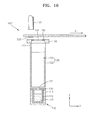
- FIG. 14 is a schematic perspective view of an organic layer deposition apparatus according to another embodiment of the present invention.
- FIG. 15 is a schematic perspective cutaway view of an organic layer deposition apparatus according to another embodiment of the present invention.
- FIG. 16 is a schematic side cross-sectional view of the organic layer deposition apparatus of FIG. 14 , according to an embodiment of the present invention.
- FIG. 17 is a schematic plan sectional view in an XZ plane of the organic layer deposition apparatus of FIG. 14 , according to an embodiment of the present invention.
- FIG. 18 is a schematic perspective cutaway view of an organic layer deposition apparatus according to another embodiment of the present invention.
- FIG. 19 is a cross-sectional view of an organic light-emitting display device manufactured by using an organic layer deposition apparatus, according to an embodiment of the present invention.
- An organic light-emitting display device includes intermediate layers, including an emission layer disposed between a first electrode and a second electrode that are arranged opposite to each other.
- the electrodes and the intermediate layers may be formed via various methods, one of which is a deposition method.
- a fine metal mask (FMM) having the same pattern as a thin film to be formed is disposed to closely contact a substrate, and a thin film material is deposited over the FMM in order to form the thin film having the desired pattern.
- the deposition method using such a FMM is generally not suitable for manufacturing larger devices using a mother glass having a size of 5G (1100 ⁇ 1300 mm) or greater.
- the mask may bend due to its own weight, thereby distorting a pattern. This is not conducive for the recent trend towards high-definition patterns.
- FIG. 1 is a schematic view of a thin film deposition system including an organic layer deposition apparatus according to an embodiment of the present invention
- FIG. 2 illustrates a modified example of the thin film deposition system of FIG. 1 .
- the thin film deposition apparatus includes a loading unit 710 , a deposition unit 730 , an unloading unit 720 , a first conveyer unit 610 and a second conveyer unit 620 .
- the loading unit 710 includes a first rack 712 , a transport robot 714 , a transport chamber 716 , and a first inversion chamber 718 .
- a plurality of substrates 500 onto which a deposition material is not applied are stacked up on the first rack 712 .
- the transport robot 714 picks up one of the substrates 500 from the first rack 712 , places it on the electrostatic chuck 600 transferred by the second conveyor unit 620 , and moves the electrostatic chuck 600 on which the substrate 500 is placed into the transport chamber 716 .
- the first inversion chamber 718 is located adjacent to the transport chamber 716 .
- the first inversion chamber 718 includes a first inversion robot 719 that inverts the electrostatic chuck 600 and then loads it onto the first conveyer unit 610 of the deposition unit 730 .
- the transport robot 714 places one of the substrates 500 on the surface of the electrostatic chuck 600 , and the electrostatic chuck 600 on which the substrate 500 is placed is loaded into the transport chamber 716 .
- the first inversion robot 719 inverts the electrostatic chuck 600 so that the substrate 500 is turned upside down in the deposition unit 730 .
- the unloading unit 720 is constituted to operate in an opposite manner to the loading unit 710 described above. Specifically, a second inversion robot 729 in a second inversion chamber 728 inverts the electrostatic chuck 600 , which has passed through the deposition unit 730 while the substrate 500 is placed on the electrostatic chuck 600 , and then moves the electrostatic chuck 600 on which the substrate 500 is placed into an ejection chamber 726 . Then, an ejection robot 724 removes the electrostatic chuck 600 on which the substrate 500 is placed from the ejection chamber 726 , separates the substrate 500 from the electrostatic chuck 600 , and then loads the substrate 500 onto the second rack 722 . The electrostatic chuck 600 separated from the substrate 500 is returned back into the loading unit 710 via the second conveyer unit 620 .
- the present invention is not limited to the above description.
- the substrate 500 when placing the substrate 500 on the electrostatic chuck 600 , the substrate 500 may be fixed onto a bottom surface of the electrostatic chuck 600 and then moved into the deposition unit 730 .
- the first inversion chamber 718 and the first inversion robot 719 , and the second inversion chamber 728 and the second inversion robot 729 are not used.
- the deposition unit 730 may include at least one deposition chamber. As illustrated in FIG. 1 , the deposition unit 730 may include a first chamber 731 . In the embodiment illustrated in FIG. 1 , first to fourth organic layer deposition apparatuses 100 , 200 , 300 , and 400 are located in the first chamber 731 . Although FIG. 1 illustrates that a total of four organic layer deposition apparatuses, i.e., the first through fourth organic layer deposition assemblies 100 through 400 , are located in the first chamber 731 , the total number of organic layer deposition apparatuses that may be installed in the first chamber 731 may vary according to a deposition material and deposition conditions. The first chamber 731 may be maintained in a vacuum state during a deposition process.
- a deposition unit 730 includes a first chamber 731 and a second chamber 732 that are connected to each other.
- first and second organic layer deposition apparatuses 100 and 200 are located in the first chamber 731
- third and fourth organic layer deposition apparatuses 300 and 400 are located in the second chamber 732 .
- the thin film deposition system may include more than two chambers.
- the electrostatic chuck 600 on which the substrate 500 is placed may be moved at least to the deposition unit 730 or may be moved sequentially to the loading unit 710 , the deposition unit 730 , and the unloading unit 720 , by the first conveyor unit 610 .
- the electrostatic chuck 600 that is separated from the substrate 500 in the unloading unit 720 is moved back to the loading unit 710 by the second conveyor unit 620 .
- FIG. 3 is a schematic perspective view of an organic layer deposition apparatus 100 according to an embodiment of the present invention
- FIG. 4 is a schematic sectional view of the organic layer deposition apparatus 100 illustrated in FIG. 3
- FIG. 5 is a schematic sectional view in an XZ plane of the organic layer deposition apparatus 100 illustrated in FIG. 3 .
- the organic layer deposition apparatus 100 includes a deposition source 110 , a deposition source nozzle unit 120 , a patterning slit sheet 150 , and an interval measuring unit 161 .
- the chamber in order to deposit a deposition material 115 that is emitted from the deposition source 110 and is discharged through the deposition source nozzle unit 120 and the patterning slit sheet 150 , onto a substrate 500 in a desired pattern, the chamber should be maintained in a high-vacuum state as in a deposition method using a fine metal mask (FMM).
- the temperature of the patterning slit sheet 150 should be sufficiently lower than the temperature of the deposition source 110 .
- the temperature of the patterning slit sheet 150 may be about 100° C. or less.
- the temperature of the patterning slit sheet 150 should be sufficiently low so as to reduce thermal expansion of the patterning slit sheet 150 .
- the substrate 500 which constitutes a deposition target on which the deposition material 115 is to be deposited, is located in the first chamber 731 .
- the substrate 500 may be a substrate for flat panel displays.
- a large substrate, such as a mother glass, for manufacturing a plurality of flat panel displays, may be used as the substrate 500 .
- Other substrates may also be employed.
- deposition may be performed while the substrate 500 or the organic layer deposition apparatus 100 is moved relative to the other.
- the size of the FMM is generally equal to the size of a substrate.
- the size of the FMM is increased as the substrate becomes larger.
- deposition may be performed while the organic layer deposition apparatus 100 or the substrate 500 is moved relative to the other.
- deposition may be continuously performed while the substrate 500 , which is disposed such as to face the organic layer deposition apparatus 100 , is moved in a Y-axis direction.
- deposition may be performed in a scanning manner while the substrate 500 is moved in a direction of arrow A in FIG. 6 (first direction).
- the patterning slit sheet 150 may be significantly smaller than a FMM used in a conventional deposition method.
- deposition is continuously performed, i.e., in a scanning manner while the substrate 500 is moved in the Y-axis direction.
- lengths of the patterning slit sheet 150 in the X-axis and Y-axis directions may be less (e.g., significantly less) than the lengths of the substrate 500 in the X-axis and Y-axis directions.
- the patterning slit sheet 150 may be formed to be smaller (e.g., significantly smaller) than a FMM used in a conventional deposition method, it is relatively easy to manufacture the patterning slit sheet 150 used in embodiments of the present invention.
- using the patterning slit sheet 150 which is smaller than a FMM used in a conventional deposition method, is more convenient in all processes, including etching and other subsequent processes, such as precise extension, welding, moving, and cleaning processes, compared to the conventional deposition method using the larger FMM. This is more advantageous for a relatively large display device.
- the deposition source 110 that contains and heats the deposition material 115 is located at an opposite side of the chamber to a side at which the substrate 500 is located. While being vaporized in the deposition source 110 , the deposition material 115 is deposited on the substrate 500 .
- the deposition source 110 includes a crucible 112 that is filled with the deposition material 115 , and a cooling block 111 that heats the crucible 112 to vaporize the deposition material 115 , which is contained in the crucible 112 , towards a side of the crucible 112 , and in particular, towards the deposition source nozzle unit 120 .
- the cooling block 111 prevents radiation of heat from the crucible 112 outside, i.e., into the first chamber 731 .
- the cooling block 111 may include a heater (not shown) that heats the crucible 111 .
- the deposition source nozzle unit 120 is located at a side of the deposition source 110 , and in particular, at the side of the deposition source 110 facing the substrate 500 .
- the deposition source nozzle unit 120 includes a plurality of deposition source nozzles 121 arranged at equal intervals in the Y-axis direction, i.e., a scanning direction of the substrate 500 .
- the deposition material 115 that is vaporized in the deposition source 110 passes through the deposition source nozzle unit 120 toward the substrate 500 .
- the deposition source nozzle unit 120 includes the plurality of deposition source nozzles 121 arranged in the Y-axis direction, that is, the scanning direction of the substrate 500 , the size of a pattern formed of the deposition material discharged through the patterning slits 151 of the patterning slit sheet 150 is affected by the size of one of the deposition source nozzles 121 (since there is only one line of deposition nozzles in the X-axis direction), and thus no shadow zone may be formed on the substrate 500 .
- the plurality of deposition source nozzles 121 are arranged in the scanning direction of the substrate 500 , even if there is a difference in flux between the deposition source nozzles 121 , the difference may be compensated for and deposition uniformity may be maintained constant.
- the patterning slit sheet 150 and a frame 155 in which the patterning slit sheet 150 is bound are located between the deposition source 110 and the substrate 500 .
- the frame 155 may be formed in a lattice shape, similar to a window frame.
- the patterning slit sheet 150 is bound inside the frame 155 .
- the patterning slit sheet 150 has a plurality of patterning slits 151 arranged in the X-axis direction.
- the deposition material 115 that is vaporized in the deposition source 110 passes through the deposition source nozzle unit 120 and the patterning slit sheet 150 toward the substrate 500 .
- the patterning slit sheet 150 may be manufactured by etching, which is the same method as used in a typical method of manufacturing an FMM, and in particular, a striped FMM.
- the total number of patterning slits 151 may be greater than the total number of deposition source nozzles 121 .
- the deposition source 110 and the deposition source nozzle unit 120 coupled to the deposition source 110 may be arranged to be separated from the patterning slit sheet 150 by a distance (e.g., a predetermined distance).
- the deposition source 110 and the deposition source nozzle unit 120 coupled to the deposition source 110 may be connected to the patterning slit sheet 150 by a connection member 135 . That is, the deposition source 110 , the deposition source nozzle unit 120 , and the patterning slit sheet 150 may be integrally formed as one body by being connected to each other via the first connection member 135 .
- the first connection member 135 guides the deposition material 115 , which is discharged through the deposition source nozzles 121 , to move straight, not to flow in the X-axis direction.
- the connection members 135 are formed on left and right sides of the deposition source 110 , the deposition source nozzle unit 120 , and the patterning slit sheet 150 to guide the deposition material 115 not to flow in the X-axis direction; however, aspects of the present invention are not limited thereto. That is, the connection member 135 may be formed as a sealed box to guide flow of the deposition material 115 both in the X-axis and Y-axis directions.
- the organic layer deposition apparatus 100 performs deposition while being moved relative to the substrate 500 .
- the patterning slit sheet 150 is separated from the substrate 500 by a distance (e.g., a predetermined distance).
- the FMM in close contact with a substrate in order to prevent formation of a shadow zone on the substrate.
- the contact may cause defects.
- the size of the mask is the same as the size of the substrate since the mask cannot be moved relative to the substrate.
- the size of the mask is increased as display devices become larger.
- the patterning slit sheet 150 is arranged to be separated from the substrate 500 by a distance (e.g., a predetermined distance).
- a mask is formed to be smaller than a substrate, and deposition is performed while the mask is moved relative to the substrate.
- the mask can be easily manufactured.
- defects caused due to the contact between a substrate and a FMM, which may occur in the conventional deposition method, may be prevented.
- the manufacturing time may be reduced.
- the interval measuring unit 161 measures an interval between the substrate 50 and the patterning slit sheet 150 .
- an organic layer is formed on the substrate 500 .
- the interval measuring unit 161 may measure the interval between the substrate 500 and the patterning slit sheet 150 while the substrate 500 is moving.
- the interval measuring unit 161 may be located within the first chamber 731 of FIG. 1 or 2 , which is in a vacuum condition, and measure the interval between the substrate 500 and the patterning slit sheet 150 .
- the interval measuring unit 161 may achieve more accurate measurement since the interval measuring unit 161 can measure the interval between the substrate 500 and the patterning slit sheet 150 within the first chamber 731 , which is in a vacuum condition.
- the interval measuring unit 161 may also increase deposition uniformity since the interval measuring unit 161 may measure in real time the interval (or gap) between the substrate 500 that is moving during a deposition process, and the patterning slit sheet 150 . While not shown specifically in FIGS.
- the organic layer deposition apparatus 100 may include a controller for adjusting (e.g., dynamically adjusting) the interval (or distance) between the substrate 500 and the patterning slit sheet 150 based on the measurement taken by the interval measuring unit 161 , such that the distance between the substrate 500 and the patterning slit sheet 150 is maintained constantly based on the measurement.
- a controller for adjusting (e.g., dynamically adjusting) the interval (or distance) between the substrate 500 and the patterning slit sheet 150 based on the measurement taken by the interval measuring unit 161 , such that the distance between the substrate 500 and the patterning slit sheet 150 is maintained constantly based on the measurement.
- the design and application of such a controller is known to those with ordinary skill in the art and will not be discussed in detail herein.
- FIGS. 6 and 7 are schematic views for illustrating a process for measuring an interval between the substrate 500 and the patterning slit sheet 150 by using the interval measuring unit 161 of FIG. 3 .
- FIG. 6 illustrates measurement of a distance between the interval measuring unit 161 and the substrate 500 by using the interval measuring unit 161
- FIG. 7 illustrates measurement of a distance between the interval measuring unit 161 and the patterning slit sheet 150 by using the interval measuring unit 161 .
- the interval measuring unit 161 is located within the first chamber 731 of FIG. 1 and is located over the substrate 500 .
- the interval measuring unit 161 first detects a sensing pattern 502 located on the bottom surface of the substrate 500 to measure a distance t 1 from the interval measuring unit 161 to the substrate 500 . Thereafter, the substrate 500 on which the sensing pattern 502 is located moves (e.g., in the A direction), and, as illustrated in FIG. 7 , the interval measuring unit 161 measures a distance t 2 from the interval measuring unit 161 to the patterning slit sheet 150 .
- the interval measuring unit 161 measures (or determines) an interval t 3 between the substrate 500 and the patterning slit sheet 150 by using the distance t 2 from the interval measuring unit 161 to the patterning slit sheet 150 and the distance t 1 from the interval measuring unit 161 to the substrate 500 .
- the interval measuring unit 161 may include a capacitive sensor or an Eddy-current sensor that are capable of measuring a distance to the substrate 500 (or the patterning slit sheet 150 ) in a vacuum condition.
- the capacitive sensor may sense flow of free electrons, which constitute a measurement target, to measure a distance to the measurement target.
- the sensing pattern 502 may be formed of metal. Accordingly, when the capacitive sensor is used as the interval measuring unit 161 , the capacitive sensor may measure the distance t 1 from the interval measuring unit 161 to the substrate 500 by sensing the sensing pattern 502 , and may measure the distance t 2 from the interval measuring unit 161 to the patterning slit sheet 150 by sensing the patterning slit sheet 150 , which is formed of metal.
- the Eddy-current sensor may sense an Eddy current on a surface of the measurement target to measure a distance to the measurement target. Accordingly, when the Eddy current sensor is used as the interval measuring unit 161 , the Eddy current sensor may measure the distance t 1 from the interval measuring unit 161 to the substrate 500 by sensing the sensing pattern 502 , and may measure the distance t 2 from the interval measuring unit 161 to the patterning slit sheet 150 by sensing the patterning slit sheet 150 , which is formed of metal.
- FIG. 8 is a schematic perspective view of an organic layer deposition apparatus 100 ′ according to another embodiment of the present invention.
- FIGS. 9 and 10 are schematic views for illustrating a process for measuring the interval between the substrate 500 and the patterning slit sheet 150 ′ by using an interval measuring unit 161 illustrated in FIG. 8 .
- the organic layer deposition apparatus 100 ′ of FIG. 8 is different from the organic layer deposition apparatus 100 of FIG. 3 in terms of a location of the interval measuring unit 161 .
- the organic layer deposition apparatus 100 of FIG. 3 includes the interval measuring unit 161 located over the substrate 500
- the organic layer deposition apparatus 100 ′ of FIG. 8 includes the interval measuring unit 161 located below the patterning slit sheet 150 ′.
- the components of the organic layer deposition apparatus 100 ′ of FIG. 8 other than the interval measuring unit 161 are substantially the same as those of the organic layer deposition apparatus 100 of FIG. 3 , so a detailed description thereof will not be provided herein.
- the interval measuring unit 161 is separated from the bottom surface of the patterning slit sheet 150 ′ and is located within the first chamber 731 .
- the interval measuring unit 161 measures a distance from the interval measuring unit 161 below the patterning slit sheet 150 ′ to the patterning slit sheet 150 ′ and a distance from the interval measuring unit 161 below the patterning slit sheet 150 ′ to the substrate 500 , thereby obtaining a distance between the patterning slit sheet 150 ′ and the substrate 500 .
- the interval measuring unit 161 is fixed within the first chamber 731 of FIG. 1 and is located below the patterning slit sheet 150 ′.
- the patterning slit sheet 150 ′ may include a through hole 152 facing the interval measuring unit 161 , and a sensing target 153 capable of covering the through hole 152 .
- the interval measuring unit 161 first senses the sensing target 153 from below the patterning slit sheet 150 ′, thereby measuring a distance t 2 from the interval measuring unit 161 to the sensing target 153 . Thereafter, as illustrated in FIG.
- the interval measuring unit 161 measures (or determines) an interval t 3 between the substrate 500 and the patterning slit sheet 150 ′ by using the distance t 2 from the interval measuring unit 161 to the patterning slit sheet 150 ′ and the distance t 1 from the interval measuring unit 161 to the substrate 500 .
- the interval measuring unit 161 may be a capacitive sensor or an Eddy-current sensor that are able to measure a distance to the substrate 500 (or the patterning slit sheet 150 ′) in a vacuum condition.
- the sensing target 153 and the sensing pattern 502 may be all formed of metal. Accordingly, the capacitive sensor or the Eddy-current sensor may sense the sensing target 153 or the sensing pattern 502 so as to measure the distance t 2 from the interval measuring unit 161 to the patterning slit sheet 150 ′ or the distance t 1 from the interval measuring unit 161 to the substrate 500 .
- FIG. 11 is a schematic view for illustrating a process for measuring an interval between the substrate 500 and a patterning slit sheet 152 by using an interval measuring unit 161 ′′ according to another embodiment of the present invention.
- the interval measuring unit 161 ′′ of FIG. 11 may be a confocal sensor.
- the confocal sensor may scan a measurement target with a laser beam by using a scanning mirror rotating at high speed, and measure a distance to the measurement target by using fluorescent or reflective rays emitted from the laser beam.
- the confocal sensor may sense an interface between different media to measure the distance to the measurement target.
- the interval measuring unit 161 ′′ which is a confocal sensor, is disposed within the first chamber 731 of FIG. 1 , which is a vacuum chamber, and is located on the substrate 500 .
- the interval measuring unit 161 ′′ which is a confocal sensor, may obtain a distance t 1 from the interval measuring unit 161 ′′ to the upper surface of the substrate 500 by sensing an interface between the upper surface of the substrate 500 and a space on the upper surface of the substrate 500 and may obtain a distance t 2 from the interval measuring unit 161 ′′ to the lower surface of the substrate 500 by sensing an interface between the lower surface of the substrate 500 and a space on the lower surface of the substrate 500 .
- the interval measuring unit 161 ′′ may measure a distance from the interval measuring unit 161 ′′ to the upper surface of the patterning slit sheet 150 by sensing the upper surface of the patterning slit sheet 150 .
- the interval measuring unit 161 ′′ may obtain an interval t 3 between the substrate 500 and the patterning slit sheet 150 by measuring the distance t 2 from the interval measuring unit 161 ′′ to the lower surface of the substrate 500 and the distance from the interval measuring unit 161 ′′ to the upper surface of the patterning slit sheet 150 .
- FIGS. 12 and 13 are schematic views for illustrating a process for measuring an interval between the substrate 500 and the patterning slit sheet 150 by using an interval measuring unit 161 ′ according to another embodiment of the present invention.
- the interval measuring unit 161 ′ of FIGS. 12 and 13 is different from the interval measuring unit 161 ′′ of FIG. 11 in that the interval measuring unit 161 ′ is located below the patterning slit sheet 150 .
- the interval sensing unit 161 ′ may include a confocal sensor or another suitable interval sensing device.
- the interval measuring unit 161 ′ measures a distance t 2 from the interval measuring unit 161 ′ to the patterning slit sheet 150 from below the patterning slit sheet 150 , before a deposition process starts. Thereafter, the patterning slit sheet 150 is moved so that the through hole 152 is located over the interval measuring unit 161 ′. Then, the interval measuring unit 161 ′ measures a distance t 1 from the interval measuring unit 161 ′ to the substrate 500 via the through hole 152 of the patterning slit sheet 150 .
- the interval measuring unit 161 ′ may obtain an interval t 3 between the substrate 500 and the patterning slit sheet 150 by measuring the distance t 2 from the interval measuring unit 161 ′ to the patterning slit sheet 150 and the distance t 1 from the interval measuring unit 161 ′ to the substrate 500 .
- FIG. 14 is a schematic perspective view of an organic layer deposition apparatus according to another embodiment of the present invention.
- the organic layer deposition apparatus according to the current embodiment of the present invention includes a plurality of organic layer deposition apparatuses, namely, first, second, and third organic layer deposition apparatuses 100 , 200 , and 300 , each of which has the structure of the organic layer deposition apparatus 100 illustrated in FIGS. 3 through 5 .
- the organic layer deposition apparatus according to the current embodiment of the present invention may include a multi-deposition source that concurrently (e.g., simultaneously) discharges deposition materials for forming an R emission layer, a G emission layer, and a B emission layer.
- the organic layer deposition apparatus includes the first organic layer deposition apparatus 100 , the second organic layer deposition apparatus 200 , and the third organic layer deposition apparatus 300 . Since each of the first organic layer deposition apparatus 100 , the second organic layer deposition apparatus 200 , and the third organic layer deposition apparatus 300 has the same structure as the organic layer deposition apparatus described with reference to FIGS. 3 through 5 , a detailed description thereof will not be provided herein.
- the deposition sources 110 of the first organic layer deposition apparatus 100 , the second organic layer deposition apparatus 200 and the third organic layer deposition apparatus 300 may contain different deposition materials, respectively.
- the first organic layer deposition apparatus 100 may contain a deposition material used to form the R emission layer
- the second organic layer deposition apparatus 200 may contain a deposition material used to form the G emission layer
- the third organic layer deposition apparatus 300 may contain a deposition material used to form the B emission layer.
- the organic layer deposition apparatus according to the current embodiment of the present invention is used, the R emission layer, the G emission layer and the B emission layer may be formed concurrently (e.g., at the same time) with a single multi-deposition source.
- the time it takes to manufacture the organic light-emitting display device may be reduced (e.g., sharply reduced).
- the organic light-emitting display device may be manufactured with a reduced number of chambers, so that equipment costs may be also reduced (e.g., markedly reduced).
- a patterning slit sheet of the first organic layer deposition apparatus 100 , a patterning slit sheet of the second organic layer deposition apparatus 200 , and a patterning slit sheet of the third organic layer deposition apparatus 300 may be arranged to be offset by a constant distance with respect to each other, in order for deposition regions corresponding to the patterning slit sheets not to overlap on the substrate 500 .
- first organic layer deposition apparatus 100 , the second organic layer deposition apparatus 200 , and the third organic layer deposition apparatus 300 are used to deposit the R emission layer, the G emission layer, and the B emission layer, respectively.
- patterning slits 151 of the first organic layer deposition apparatus 100 , patterning slits 251 of the second organic layer deposition apparatus 200 , and patterning slits 351 of the third organic layer deposition apparatus 300 are arranged not to be aligned with respect to each other, in order to form the R emission layer, the G emission layer and the B emission layer in different regions of the substrate 500 .
- the deposition materials used to form the R emission layer, the G emission layer, and the B emission layer may have different deposition temperatures. Therefore, the temperatures of the deposition sources of the respective first, second, and third organic layer deposition assemblies 100 , 200 , and 300 may be set to be different.
- an organic layer deposition apparatus may include a plurality of organic layer deposition apparatuses, each of which contains a different deposition material.
- an organic layer deposition apparatus may include five organic layer deposition apparatuses respectively containing materials for a R emission layer, a G emission layer, a B emission layer, an auxiliary layer (R′) of the R emission layer, and an auxiliary layer (G′) of the G emission layer.
- a plurality of thin films may be formed concurrently (e.g., at the same time) with a plurality of organic layer deposition apparatuses, and thus manufacturing yield and deposition efficiency may be improved.
- the overall manufacturing process may be simplified, and the manufacturing cost may be reduced.
- FIG. 15 is a schematic perspective cutaway view of an organic layer deposition apparatus 100 ′′ according to another embodiment of the present invention
- FIG. 16 is a schematic side cross-sectional view of the organic layer deposition apparatus 100 ′′
- FIG. 17 is a schematic sectional view in an XZ plane of the organic layer deposition apparatus 100 ′′.
- the organic layer deposition apparatus 100 ′′ includes a deposition source 110 , a deposition source nozzle unit 120 ′, a barrier plate assembly 130 , and a patterning slit sheet 150 having a plurality of patterning slits 151 .
- all the components of the organic layer deposition apparatus 100 ′′ may be located within a chamber that is maintained at an appropriate degree of vacuum.
- the chamber is maintained at an appropriate vacuum in order to allow a deposition material to move in a substantially straight line through the organic layer deposition apparatus 100 ′′.
- the substrate 500 which constitutes a deposition target on which the deposition material 115 is to be deposited, is transferred by the electrostatic chuck 600 .
- the substrate 500 may be a substrate for flat panel displays.
- a large substrate, such as a mother glass, for manufacturing a plurality of flat panel displays, may be used as the substrate 500 .
- Other substrates may also be employed.
- the substrate 500 or the organic layer deposition apparatus 100 ′′ may be moved relative to the other.
- the substrate 500 may be moved in a direction of an arrow A, relative to the organic layer deposition apparatus 100 ′′.
- the patterning slit sheet 150 may be smaller (e.g., significantly smaller) than a FMM used in a conventional deposition method.
- deposition is continuously performed, i.e., in a scanning manner while the substrate 500 is moved in the Y-axis direction.
- a length of the patterning slit sheet 150 in the Y-axis direction may be less (e.g., significantly less) than a length of the substrate 500 provided that a width of the patterning slit sheet 150 in the X-axis direction and a width of the substrate 500 in the X-axis direction are substantially equal to each other.
- deposition may be performed on the entire substrate 500 in a scanning manner while the substrate 500 or the organic layer deposition apparatus 100 ′′ is moved relative each other.
- the patterning slit sheet 150 may be formed to be smaller (e.g., significantly smaller) than a FMM used in a conventional deposition method, it is relatively easy to manufacture the patterning slit sheet 150 used in embodiments of the present invention.
- using the patterning slit sheet 150 which is smaller than a FMM used in a conventional deposition method, is more convenient in all processes, including etching and other subsequent processes, such as precise extension, welding, moving, and cleaning processes, compared to the conventional deposition method using the larger FMM. This is more advantageous for a relatively large display device.
- the deposition source 110 that contains and heats the deposition material 115 is located at an opposite side of the first chamber to a side at which the substrate 500 is located.
- the deposition source 110 includes a crucible 112 that is filled with the deposition material 115 , and a cooling block 111 surrounding the crucible 112 .
- the cooling block 111 prevents radiation of heat from the crucible 112 outside, e.g., into the first chamber.
- the cooling block 111 may include a heater (not shown) that heats the crucible 112 .
- the deposition source nozzle unit 120 ′ is located at a side of the deposition source 110 , and in particular, at the side of the deposition source 110 facing the substrate 500 .
- the deposition source nozzle unit 120 ′ includes a plurality of deposition source nozzles 121 ′ arranged at equal intervals in the X-axis direction.
- the deposition material 115 that is vaporized in the deposition source 110 passes through the deposition source nozzles 121 ′ of the deposition source nozzle unit 120 ′ toward the substrate 500 , which constitutes a target on which the deposition material 115 is to be deposited.
- the barrier plate assembly 130 is disposed at a side of the deposition source nozzle unit 120 ′.
- the barrier plate assembly 130 includes a plurality of barrier plates 131 , and a barrier plate frame 132 that covers sides of the barrier plates 131 .
- the plurality of barrier plates 131 may be arranged parallel to each other at equal intervals in the X-axis direction.
- each of the barrier plates 131 may be arranged parallel to an YZ plane in FIG. 15 , and may have a rectangular shape.
- the plurality of barrier plates 131 arranged as described above partition the space between the deposition source nozzle unit 120 ′ and the patterning slit sheet 150 into a plurality of sub-deposition spaces S (for example, see FIG. 17 ).
- the deposition space is divided by the barrier plates 131 into the sub-deposition spaces S that respectively correspond to the deposition source nozzles 121 ′ through which the deposition material 115 is discharged.
- the barrier plates 131 may be respectively located between adjacent deposition source nozzles 121 ′.
- each of the deposition source nozzles 121 ′ may be located between two adjacent barrier plates 131 .
- the deposition source nozzles 121 ′ may be respectively located at the midpoint between two adjacent barrier plates 131 .
- the present invention is not limited to this structure.
- a plurality of deposition source nozzles 121 ′ may be located between two adjacent barrier plates 131 .
- the deposition source nozzles 121 ′ may be also respectively located at the midpoint between two adjacent barrier plates 131 .
- the barrier plates 131 partition the space between the deposition source nozzle unit 120 ′ and the patterning slit sheet 150 into the plurality of sub-deposition spaces S, the deposition material 115 discharged through each of the deposition source nozzles 121 ′ is not mixed with the deposition material 115 discharged through the other deposition source nozzles 121 ′, and passes through the patterning slits 151 so as to be deposited on the substrate 500 .
- the barrier plates 131 guide the deposition material 115 , which is discharged through the deposition source nozzles 121 ′, to move straight, not to flow in the X-axis direction.
- the deposition material 115 is forced to move straight by installing the barrier plates 131 , so that a smaller shadow zone may be formed on the substrate 500 compared to a case where no barrier plates are installed.
- the organic layer deposition apparatus 100 ′′ and the substrate 500 can be separated from each other by a distance (e.g., a predetermined distance). This will be described later in detail.
- the barrier plate frame 132 which forms sides of the barrier plates 131 , maintains the positions of the barrier plates 131 , and guides the deposition material 115 , which is discharged through the deposition source nozzles 121 ′, not to flow in the Y-axis direction.
- the barrier plate frame 132 in the embodiment of FIG. 15 includes two opposing barrier frame plates that are spaced from each other along the Y-axis direction with the barrier plates 131 located therebetween.
- the barrier frame plate on the left side in FIG. 15 is cutaway and one side of a second connection member 133 is not shown for convenience of illustration.
- the deposition source nozzle unit 120 ′ and the barrier plate assembly 130 may be separated from each other by a distance (e.g., a predetermined distance). This may prevent the heat radiated from the deposition source unit 110 from being conducted to the barrier plate assembly 130 .
- a distance e.g., a predetermined distance.
- an appropriate heat insulator (not shown) may be further located between the deposition source nozzle unit 120 ′ and the barrier plate assembly 130 . In this case, the deposition source nozzle unit 120 ′ and the barrier plate assembly 130 may be bound together with the heat insulator therebetween.
- the barrier plate assembly 130 may be constructed to be detachable from the organic layer deposition apparatus 100 ′′.
- the deposition space is enclosed by using the barrier plate assembly 130 , so that the deposition material 115 that remains undeposited is mostly deposited within the barrier plate assembly 130 .
- the barrier plate assembly 130 since the barrier plate assembly 130 is constructed to be detachable from the organic layer deposition apparatus 100 ′′, when a large amount of the deposition material 115 lies in the barrier plate assembly 130 after a long deposition process, the barrier plate assembly 130 may be detached from the organic layer deposition apparatus 100 ′′ and then placed in a separate deposition material recycling apparatus in order to recover the deposition material 115 . Due to the structure of the organic layer deposition apparatus 100 ′′ according to the present embodiment, a reuse rate of the deposition material 115 may be increased, so that the deposition efficiency may be improved, and thus the manufacturing cost may be reduced.
- the patterning slit sheet 150 and a frame 155 in which the patterning slit sheet 150 is bound are located between the deposition source 110 and the substrate 500 .
- the frame 155 may be formed in a lattice shape, similar to a window frame.
- the patterning slit sheet 150 is bound inside the frame 155 .
- the patterning slit sheet 150 has a plurality of patterning slits 151 arranged in the X-axis direction. Each of the patterning slits 151 extends in the Y-axis direction.
- the deposition material 115 that has been vaporized in the deposition source 110 and passed through the deposition source nozzle 121 ′ passes through the patterning slits 151 toward the substrate 500 .
- the patterning slit sheet 150 may be formed of a metal thin film.
- the patterning slit sheet 150 is fixed to the frame 155 such that a tensile force is exerted thereon.
- the patterning frame 155 may exert a stretching force to the patterning slit sheet 150 towards the periphery of the patterning slit sheet 150 .
- the patterning slits 151 may be formed by etching the patterning slit sheet 150 to have a stripe pattern.
- the total number of patterning slits 151 may be greater than the total number of deposition source nozzles 121 ′. In addition, there may be a greater number of patterning slits 151 than deposition source nozzles 121 ′ located between two adjacent barrier plates 131 . The number of patterning slits 151 may be equal to the number of deposition patterns to be formed on the substrate 500 .
- the barrier plate assembly 130 and the patterning slit sheet 150 may be arranged to be separated from each other by a distance (e.g., a predetermined distance).
- the barrier plate assembly 130 and the patterning slit sheet 150 may be connected by a second connection member 133 .
- the temperature of the barrier plate assembly 130 may increase to 100° C. or higher due to the deposition source 110 whose temperature is high.
- the barrier plate assembly 130 and the patterning slit sheet 150 are separated from each other by a distance (e.g., a predetermined distance).
- the organic layer deposition apparatus 100 ′′ performs deposition while being moved relative to the substrate 500 .
- the patterning slit sheet 150 is separated from the substrate 500 by a distance (e.g., a predetermined distance).
- the barrier plates 131 are arranged between the deposition source nozzle unit 120 ′ and the patterning slit sheet 150 to force the deposition material 115 to move in a straight direction.
- the size of the shadow zone that may be formed on the substrate 500 may be reduced (e.g., sharply reduced).
- a conventional deposition method using a FMM deposition is performed with the FMM in close contact with a substrate in order to prevent formation of a shadow zone on the substrate.
- the contact may cause defects, such as scratches on patterns formed on the substrate.
- the size of the mask is the same as the size of the substrate since the mask cannot be moved relative to the substrate. Thus, the size of the mask is increased as display devices become larger. However, it is not easy to manufacture such a large mask.
- the patterning slit sheet 150 is arranged to be separated from the substrate 500 by a distance (e.g., a predetermined distance). This may be facilitated by installing the barrier plates 131 to reduce the size of the shadow zone formed on the substrate 500 .
- the patterning slit sheet 150 when the patterning slit sheet 150 is manufactured to be smaller than the substrate 500 , the patterning slit sheet 150 may be moved relative to the substrate 500 during deposition. Thus, it is no longer necessary to manufacture a large FMM as used in the conventional deposition method. In addition, since the substrate 500 and the patterning slit sheet 150 are separated from each other, defects caused due to contact therebetween may be prevented. In addition, since it is unnecessary to contact the substrate 500 with the patterning slit sheet 150 during a deposition process, the manufacturing speed may be improved.
- FIG. 18 is a schematic perspective cutaway view of an organic layer deposition apparatus 100 ′′′ according to another embodiment of the present invention.
- the organic layer deposition apparatus 100 ′′′ includes a deposition source 110 , a deposition source nozzle unit 120 ′′, a first barrier plate assembly 130 , a second barrier plate assembly 140 , and a patterning slit sheet 150 .
- all the components of the organic layer deposition apparatus 500 may be located within a chamber that is maintained at an appropriate degree of vacuum.
- the chamber is maintained at an appropriate vacuum in order to allow a deposition material to move in a substantially straight line through the organic layer deposition apparatus 100 ′.
- the substrate 500 which constitutes a deposition target on which a deposition material 115 is to be deposited, is located in the chamber.
- the deposition source 115 that contains and heats the deposition material 110 is located at an opposite side of the chamber to that at which the substrate 500 is located.
- Structures of the deposition source 110 and the patterning slit sheet 150 are substantially the same as those in the embodiment described with reference to FIG. 15 , and thus a detailed description thereof will not be provided here.
- the first barrier plate assembly 130 is also substantially the same as the barrier plate assembly 130 of the embodiment described with reference to FIG. 15 , and thus a detailed description thereof will not be provided here.
- the second barrier plate assembly 140 is located at a side of the first barrier plate assembly 130 .
- the second barrier plate assembly 140 includes a plurality of second barrier plates 141 , and a second barrier plate frame 142 that covers sides of the second barrier plates 141 .
- the second barrier wall frame 142 may be frame shaped to surround the plurality of second barrier plates 141 .
- a schematic cutaway view of the second barrier wall frame 142 is shown for convenience of illustration.
- the plurality of second barrier plates 141 may be arranged parallel to each other at equal intervals in the X-axis direction.
- each of the second barrier plates 141 may be formed to extend in the YZ plane in FIG. 18 , i.e., perpendicular to the X-axis direction.
- the deposition space is divided by the first barrier plates 131 and the second barrier plates 141 into sub-deposition spaces that respectively correspond to the deposition source nozzles 121 ′′ through which the deposition material 115 is discharged.
- the second barrier plates 141 may be arranged to correspond respectively to the first barrier plates 131 .
- the second barrier plates 141 may be respectively aligned with the first barrier plates 131 to be parallel thereto on the same plane as the first barrier plates 131 .
- Each pair of the corresponding first and second barrier plates 131 and 141 may be located on the same plane.
- the first barrier plates 131 and the second barrier plates 141 are respectively illustrated as having the same thickness in the X-axis direction, aspects of the present invention are not limited thereto.
- the second barrier plates 141 which need to be accurately aligned with the patterning slits 151 , may be formed to be relatively thin, whereas the first barrier plates 131 , which do not need to be precisely aligned with the patterning slits 151 , may be formed to be relatively thick. This makes it easier to manufacture the organic layer deposition apparatus.
- a plurality of the above-described organic layer deposition apparatuses 100 ′′′ may be successively located in the first chamber 731 .
- the organic layer deposition apparatuses 100 , 200 , 300 and 400 may be used to deposit different deposition materials, respectively.
- the organic layer deposition apparatuses 100 , 200 , 300 and 400 may have different patterning slit patterns, so that pixels of different colors, for example, red, green and blue, may be concurrently (e.g., simultaneously) defined through a film deposition process.
- FIG. 19 is a cross-sectional view of an organic light-emitting display device manufactured by using an organic layer deposition apparatus, according to an embodiment of the present invention.
- the active matrix organic light-emitting display device is formed on a substrate 30 .
- the substrate 30 may be formed of a transparent material, for example, glass, plastic or metal.
- An insulating layer 31 such as a buffer layer, is formed on an entire surface of the substrate 30 .
- a thin film transistor (TFT) 40 , a capacitor 50 , and an organic light-emitting diode (OLED) 60 are located on the insulating layer 31 , as illustrated in FIG. 19 .
- a semiconductor active layer 41 is formed on an upper surface of the insulating layer 31 in a predetermined pattern.
- a gate insulating layer 32 is formed to cover the semiconductor active layer 41 .
- the active layer 41 may include a p-type or n-type semiconductor material.
- a gate electrode 42 of the TFT 40 is formed in a region of the gate insulating layer 32 corresponding to the active layer 41 .
- An interlayer insulating layer 33 is formed to cover the gate electrode 42 .
- the interlayer insulating layer 33 and the gate insulating layer 32 are etched by, for example, dry etching, to form a contact hole exposing parts of the active layer 41 .
- a source/drain electrode 43 is formed on the interlayer insulating layer 33 to contact the active layer 41 through the contact hole.
- a passivation layer 34 is formed to cover the source/drain electrode 43 , and is etched to expose a part of the drain electrode 43 .
- An insulating layer (not shown) may be further formed on the passivation layer 34 so as to planarize the passivation layer 34 .
- the OLED 60 displays image information (e.g., predetermined image information) by emitting red, green, or blue light as current flows.
- the OLED 60 includes a first electrode 61 located on the passivation layer 34 .
- the first electrode 61 is electrically connected to the drain electrode 43 of the TFT 40 .
- a pixel defining layer 35 is formed to cover the first electrode 61 .
- An opening 64 is formed in the pixel defining layer 35 , and then an organic emission layer 63 is formed in a region defined by the opening 64 .
- a second electrode 62 is formed on the organic emission layer 63 .
- the pixel defining layer 35 which defines individual pixels, is formed of an organic material.
- the pixel defining layer 35 also planarizes the surface of a region of the substrate 30 where the first electrode 61 is formed, and in particular, the surface of the passivation layer 34 .
- the first electrode 61 and the second electrode 62 are insulated from each other, and respectively apply voltages of opposite polarities to the organic emission layer 63 to induce light emission.
- the organic emission layer 63 may be formed of a low-molecular weight organic material or a high-molecular weight organic material.
- the organic emission layer 63 may have a single or multi-layer structure including at least one selected from the group consisting of a hole injection layer (HIL), a hole transport layer (HTL), an emission layer (EML), an electron transport layer (ETL), and an electron injection layer (EIL).
- HIL hole injection layer
- HTL hole transport layer
- EML emission layer
- ETL electron transport layer
- EIL electron injection layer
- Examples of available organic materials may include copper phthalocyanine (CuPc), N,N′-di(naphthalene-1-yl)-N,N′-diphenyl-benzidine (NPB), tris-8-hydroxyquinoline aluminum (Alq3), and the like.
- the second electrode 62 may be formed by the same deposition method as used to form the organic emission layer 63 .
- the first electrode 61 may function as an anode, and the second electrode 62 may function as a cathode. Alternatively, the first electrode 61 may function as a cathode, and the second electrode 62 may function as an anode.
- the first electrode 61 may be patterned to correspond to individual pixel regions, and the second electrode 62 may be formed to cover all the pixels.
- the first electrode 61 may be formed as a transparent electrode or a reflective electrode.
- a transparent electrode may be formed of indium tin oxide (ITO), indium zinc oxide (IZO), zinc oxide (ZnO), or indium oxide (In 2 O 3 ).
- a reflective electrode may be formed by forming a reflective layer from silver (Ag), magnesium (Mg), aluminum (Al), platinum (Pt), palladium (Pd), gold (Au), nickel (Ni), neodymium (Nd), iridium (Ir), chromium (Cr) or a compound thereof and forming a layer of ITO, IZO, ZnO, or In 2 O 3 on the reflective layer.
- the first electrode 61 may be formed by forming a layer by, for example, sputtering, and then patterning the layer by, for example, photolithography.
- the second electrode 62 may also be formed as a transparent electrode or a reflective electrode.
- the second electrode 62 functions as a cathode.
- a transparent electrode may be formed by depositing a metal having a low work function, such as lithium (Li), calcium (Ca), lithium fluoride/calcium (LiF/Ca), lithium fluoride/aluminum (LiF/Al), aluminum (Al), silver (Ag), magnesium (Mg), or a compound thereof on a surface of the intermediate layer 63 and forming an auxiliary electrode layer or a bus electrode line thereon from ITO, IZO, ZnO, In 2 O 3 , or the like.
- a metal having a low work function such as lithium (Li), calcium (Ca), lithium fluoride/calcium (LiF/Ca), lithium fluoride/aluminum (LiF/Al), aluminum (Al), silver (Ag), magnesium (Mg), or a compound thereof on a surface of the intermediate layer
- the reflective layer may be formed by depositing Li, Ca, LiF/Ca, LiF/Al, Al, Ag, Mg, or a compound thereof on the entire surface of the organic emission layer 63 .
- the second electrode 62 may be formed by using the same deposition method as used to form the organic emission layer 63 described above.
- the organic layer deposition apparatus may be easily manufactured and may be simply applied to the manufacture of large-sized display devices on a mass scale.
- the organic layer deposition apparatus may improve manufacturing yield and deposition efficiency and may allow deposition materials to be reused.
- the organic layer deposition apparatuses according to the embodiments of the present invention described above may be applied to form an organic layer or an inorganic layer of an organic TFT, and to form layers from various materials.
- any suitable one of the thin film deposition apparatuses 100 FIGS. 3-7 ), 100 ′ ( FIG. 8-10 ), 100 , 200 , 300 ( FIG. 14 ), 100 ′′ ( FIGS. 15-17 ) and 100 ′′′ ( FIG. 18 ) or those depicted in FIGS. 11-13 may be used as one or more of the thin film apparatuses 100 , 200 , 300 or 400 of FIGS. 1 and 2 , or as additional thin film apparatuses not specifically shown in FIGS. 1 and 2 . Further, as discussed above in reference to FIGS.
- each thin film deposition apparatus described herein may include a controller for adjusting (e.g., dynamically adjusting) the interval (or distance) between the substrate and the patterning slit sheet based on the measurement generated by the interval measuring unit, such that the distance between the substrate and the patterning slit sheet can be maintained constantly based on the measurement.
- a controller for adjusting e.g., dynamically adjusting the interval (or distance) between the substrate and the patterning slit sheet based on the measurement generated by the interval measuring unit, such that the distance between the substrate and the patterning slit sheet can be maintained constantly based on the measurement.
Abstract
Description
Claims (21)
Applications Claiming Priority (2)
| Application Number | Priority Date | Filing Date | Title |
|---|---|---|---|
| KR10-2010-0127090 | 2010-12-13 | ||
| KR1020100127090A KR20120065789A (en) | 2010-12-13 | 2010-12-13 | Apparatus for organic layer deposition |
Publications (2)
| Publication Number | Publication Date |
|---|---|
| US20120145077A1 US20120145077A1 (en) | 2012-06-14 |
| US8852687B2 true US8852687B2 (en) | 2014-10-07 |
Family
ID=46198032
Family Applications (1)
| Application Number | Title | Priority Date | Filing Date |
|---|---|---|---|
| US13/198,591 Active 2032-03-28 US8852687B2 (en) | 2010-12-13 | 2011-08-04 | Organic layer deposition apparatus |
Country Status (2)
| Country | Link |
|---|---|
| US (1) | US8852687B2 (en) |
| KR (1) | KR20120065789A (en) |
Cited By (3)
| Publication number | Priority date | Publication date | Assignee | Title |
|---|---|---|---|---|
| US20140284561A1 (en) * | 2013-03-20 | 2014-09-25 | Samsung Display Co., Ltd. | Method of manufacturing organic light-emitting display apparatus, and organic light-emitting display apparatus manufactured by the method |
| CN107815640A (en) * | 2016-09-12 | 2018-03-20 | 三星显示有限公司 | Mask and manufacture include the method for the mask assembly of mask |
| US11850620B1 (en) * | 2018-12-03 | 2023-12-26 | Mochii, Inc. | Coating of samples for microscopy |
Families Citing this family (33)
| Publication number | Priority date | Publication date | Assignee | Title |
|---|---|---|---|---|
| TWI475124B (en) | 2009-05-22 | 2015-03-01 | Samsung Display Co Ltd | Thin film deposition apparatus |
| TWI472639B (en) | 2009-05-22 | 2015-02-11 | Samsung Display Co Ltd | Thin film deposition apparatus |
| US8882920B2 (en) * | 2009-06-05 | 2014-11-11 | Samsung Display Co., Ltd. | Thin film deposition apparatus |
| KR101117719B1 (en) * | 2009-06-24 | 2012-03-08 | 삼성모바일디스플레이주식회사 | Apparatus for thin layer deposition |
| JP5328726B2 (en) | 2009-08-25 | 2013-10-30 | 三星ディスプレイ株式會社 | Thin film deposition apparatus and organic light emitting display device manufacturing method using the same |
| JP5677785B2 (en) | 2009-08-27 | 2015-02-25 | 三星ディスプレイ株式會社Samsung Display Co.,Ltd. | Thin film deposition apparatus and organic light emitting display device manufacturing method using the same |
| US8696815B2 (en) * | 2009-09-01 | 2014-04-15 | Samsung Display Co., Ltd. | Thin film deposition apparatus |
| US8876975B2 (en) | 2009-10-19 | 2014-11-04 | Samsung Display Co., Ltd. | Thin film deposition apparatus |
| KR101084184B1 (en) | 2010-01-11 | 2011-11-17 | 삼성모바일디스플레이주식회사 | Apparatus for thin layer deposition |
| KR101174875B1 (en) | 2010-01-14 | 2012-08-17 | 삼성디스플레이 주식회사 | Apparatus for thin layer deposition, method for manufacturing of organic light emitting display apparatus using the same, and organic light emitting display apparatus manufactured by the method |
| KR101193186B1 (en) | 2010-02-01 | 2012-10-19 | 삼성디스플레이 주식회사 | Apparatus for thin layer deposition, method for manufacturing of organic light emitting display apparatus using the same, and organic light emitting display apparatus manufactured by the method |
| KR101156441B1 (en) | 2010-03-11 | 2012-06-18 | 삼성모바일디스플레이주식회사 | Apparatus for thin layer deposition |
| KR101202348B1 (en) | 2010-04-06 | 2012-11-16 | 삼성디스플레이 주식회사 | Apparatus for thin layer deposition and method for manufacturing of organic light emitting display apparatus using the same |
| US8894458B2 (en) | 2010-04-28 | 2014-11-25 | Samsung Display Co., Ltd. | Thin film deposition apparatus, method of manufacturing organic light-emitting display device by using the apparatus, and organic light-emitting display device manufactured by using the method |
| KR101223723B1 (en) | 2010-07-07 | 2013-01-18 | 삼성디스플레이 주식회사 | Apparatus for thin layer deposition, method for manufacturing of organic light emitting display apparatus using the same, and organic light emitting display apparatus manufactured by the method |
| KR101738531B1 (en) | 2010-10-22 | 2017-05-23 | 삼성디스플레이 주식회사 | Method for manufacturing of organic light emitting display apparatus, and organic light emitting display apparatus manufactured by the method |
| KR101723506B1 (en) | 2010-10-22 | 2017-04-19 | 삼성디스플레이 주식회사 | Apparatus for organic layer deposition and method for manufacturing of organic light emitting display apparatus using the same |
| KR20120045865A (en) | 2010-11-01 | 2012-05-09 | 삼성모바일디스플레이주식회사 | Apparatus for organic layer deposition |
| KR20120065789A (en) | 2010-12-13 | 2012-06-21 | 삼성모바일디스플레이주식회사 | Apparatus for organic layer deposition |
| KR101760897B1 (en) | 2011-01-12 | 2017-07-25 | 삼성디스플레이 주식회사 | Deposition source and apparatus for organic layer deposition having the same |
| US9064740B2 (en) * | 2011-04-20 | 2015-06-23 | Koninklijke Philips N.V. | Measurement device and method for vapour deposition applications |
| KR101840654B1 (en) | 2011-05-25 | 2018-03-22 | 삼성디스플레이 주식회사 | Apparatus for organic layer deposition and method for manufacturing of organic light emitting display apparatus using the same |
| KR101852517B1 (en) | 2011-05-25 | 2018-04-27 | 삼성디스플레이 주식회사 | Apparatus for organic layer deposition and method for manufacturing of organic light emitting display apparatus using the same |
| KR101857249B1 (en) | 2011-05-27 | 2018-05-14 | 삼성디스플레이 주식회사 | Patterning slit sheet assembly, apparatus for organic layer deposition, method for manufacturing organic light emitting display apparatus and organic light emitting display apparatus |
| KR101826068B1 (en) | 2011-07-04 | 2018-02-07 | 삼성디스플레이 주식회사 | Apparatus for thin layer deposition |
| KR101959975B1 (en) * | 2012-07-10 | 2019-07-16 | 삼성디스플레이 주식회사 | Apparatus for organic layer deposition, method for manufacturing of organic light emitting display apparatus using the same, and organic light emitting display apparatus manufactured by the method |
| KR101959974B1 (en) * | 2012-07-10 | 2019-07-16 | 삼성디스플레이 주식회사 | Apparatus for organic layer deposition, method for manufacturing of organic light emitting display apparatus using the same, and organic light emitting display apparatus manufactured by the method |
| DE102012107824B3 (en) * | 2012-08-24 | 2014-02-06 | Technische Universität Braunschweig Carolo-Wilhelmina | Method for coating a substrate with a plurality of material layers and multi-material delivery device therefor |
| KR102013318B1 (en) * | 2012-09-20 | 2019-08-23 | 삼성디스플레이 주식회사 | Apparatus for thin layer deposition, method for manufacturing of organic light emitting display apparatus using the same, and organic light emitting display apparatus |
| KR101994838B1 (en) * | 2012-09-24 | 2019-10-01 | 삼성디스플레이 주식회사 | Apparatus for organic layer deposition, method for manufacturing of organic light emitting display apparatus using the same, and organic light emitting display apparatus manufactured by the method |
| KR20140118551A (en) * | 2013-03-29 | 2014-10-08 | 삼성디스플레이 주식회사 | Deposition apparatus, method for manufacturing organic light emitting display apparatus and organic light emitting display apparatus |
| KR102107104B1 (en) | 2013-06-17 | 2020-05-07 | 삼성디스플레이 주식회사 | Apparatus for organic layer deposition, and method for manufacturing of organic light emitting display apparatus using the same |
| KR102501111B1 (en) | 2015-12-28 | 2023-02-16 | 엘지디스플레이 주식회사 | Camera module integrated liquid display device and manufacturing method thereof |
Citations (462)
| Publication number | Priority date | Publication date | Assignee | Title |
|---|---|---|---|---|
| JPS57194252U (en) | 1981-06-02 | 1982-12-09 | ||
| US4416217A (en) | 1981-07-31 | 1983-11-22 | Ulvac Seimaku Kabushiki Kaisha | Apparatus for forming an inhomogeneous optical layer |
| US4468648A (en) | 1982-10-15 | 1984-08-28 | Mamoru Uchikune | Switchable permanent magnetic chuck |
| US4687939A (en) | 1983-11-07 | 1987-08-18 | Hitachi, Ltd. | Method and apparatus for forming film by ion beam |
| US4792378A (en) | 1987-12-15 | 1988-12-20 | Texas Instruments Incorporated | Gas dispersion disk for use in plasma enhanced chemical vapor deposition reactor |
| US4901667A (en) | 1985-08-09 | 1990-02-20 | Hitachi, Ltd. | Surface treatment apparatus |
| JPH02247372A (en) | 1989-03-17 | 1990-10-03 | Mitsubishi Electric Corp | Thin film formation |
| JPH04272170A (en) | 1991-02-25 | 1992-09-28 | Tokai Carbon Co Ltd | Graphite crucible for vacuum vapor deposition |
| JPH0598425A (en) | 1991-10-04 | 1993-04-20 | Mitsubishi Electric Corp | Thin film forming device |
| JPH0522405Y2 (en) | 1985-12-05 | 1993-06-08 | ||
| JPH05230628A (en) | 1992-02-18 | 1993-09-07 | Fujitsu Ltd | Metal film forming device and metal recovery method in metal film forming device |
| US5454847A (en) | 1992-09-18 | 1995-10-03 | Alcatel Alsthom Compagnie Generale D'electricite | Vapor deposition method for depositing a film of fluorine-containing glass on a substrate |
| US5460654A (en) | 1992-07-01 | 1995-10-24 | Fujitsu Limited | Apparatus for generating raw material gas used in apparatus for growing thin film |
| US5487609A (en) | 1991-05-13 | 1996-01-30 | Thk Co., Ltd. | Slide unit for linear motion |
| JPH0827568B2 (en) | 1990-07-02 | 1996-03-21 | 三田工業株式会社 | Transfer paper separating device in image forming apparatus |
| JPH0995776A (en) | 1995-09-29 | 1997-04-08 | Sony Corp | Vacuum deposition device |
| JPH1050478A (en) | 1996-04-19 | 1998-02-20 | Toray Ind Inc | Organic field emission element and manufacture thereof |
| US5742129A (en) | 1995-02-21 | 1998-04-21 | Pioneer Electronic Corporation | Organic electroluminescent display panel with projecting ramparts and method for manufacturing the same |
| JPH10120171A (en) | 1996-10-15 | 1998-05-12 | Balzers Ag | Device for conveying base plate in vacuum treatment system |
| JPH10270535A (en) | 1997-03-25 | 1998-10-09 | Nikon Corp | Moving stage device and circuit-device manufacture using the same |
| WO1999025894A1 (en) | 1997-11-17 | 1999-05-27 | The Trustees Of Princeton University | Low pressure vapor phase deposition of organic thin films |
| JPH11144865A (en) | 1997-11-05 | 1999-05-28 | Casio Comput Co Ltd | Manufacture of organic electroluminescent element |
| JP2000068054A (en) | 1998-08-26 | 2000-03-03 | Hokuriku Electric Ind Co Ltd | Manufacture of el element |
| US6045671A (en) | 1994-10-18 | 2000-04-04 | Symyx Technologies, Inc. | Systems and methods for the combinatorial synthesis of novel materials |
| KR20000023929A (en) | 1999-10-29 | 2000-05-06 | 최중호 | Apparatus and method for emitting odor |
| KR100257219B1 (en) | 1997-10-23 | 2000-05-15 | 박용관 | Method and device for making a safety operation of a polyethylene gas pipe valve arrangement |
| US6091195A (en) | 1997-02-03 | 2000-07-18 | The Trustees Of Princeton University | Displays having mesa pixel configuration |
| US6099649A (en) | 1997-12-23 | 2000-08-08 | Applied Materials, Inc. | Chemical vapor deposition hot-trap for unreacted precursor conversion and effluent removal |
| JP2000282219A (en) | 1999-04-02 | 2000-10-10 | Canon Inc | Method for reproducing mask for organic film vacuum deposition and device therefor |
| KR20000019254U (en) | 1999-04-07 | 2000-11-06 | 손대균 | Roundin WheeL |
| JP2000323277A (en) | 1999-05-12 | 2000-11-24 | Pioneer Electronic Corp | Organic electroluminescent multi-color display and its manufacture |
| JP2001028325A (en) | 1999-07-13 | 2001-01-30 | Tdk Corp | Method and device for transfer chip part, and electrode- forming device |
| JP2001052862A (en) | 1999-08-04 | 2001-02-23 | Hokuriku Electric Ind Co Ltd | Manufacture of organic el element and device therefor |
| JP2001093667A (en) | 1999-09-28 | 2001-04-06 | Sanyo Electric Co Ltd | Organic light-emitting element, device and method for manufacturing the same |
| KR20010030175A (en) | 1999-09-01 | 2001-04-16 | 이데이 노부유끼 | Plane display unit and plane display apparatus |
| KR20010039298A (en) | 1999-10-29 | 2001-05-15 | 김영남 | Field emission display |
| US20010004186A1 (en) | 1999-12-10 | 2001-06-21 | Song Gi-Young | Shadow mask frame assembly for flat CRT |
| US20010006827A1 (en) | 1999-12-27 | 2001-07-05 | Semiconductor Energy Laboratory Co., Ltd. | Film formation apparatus and method for forming a film |
| KR20010059939A (en) | 1999-12-30 | 2001-07-06 | 송문섭 | Mobile station for mobile communication system |
| US6274198B1 (en) | 1997-02-24 | 2001-08-14 | Agere Systems Optoelectronics Guardian Corp. | Shadow mask deposition |
| US6280821B1 (en) | 1998-09-10 | 2001-08-28 | Ppg Industries Ohio, Inc. | Reusable mask and method for coating substrate |
| US20010019807A1 (en) | 1999-12-24 | 2001-09-06 | Tsutomu Yamada | Deposition mask and manufacturing method thereof, and electroluminescence display device and manufacturing method thereof |
| US20010026638A1 (en) | 2000-03-28 | 2001-10-04 | Katsuya Sangu | Positioning apparatus used in a process for producing multi-layered printed circuit board and method of using the same |
| US20010034175A1 (en) | 2000-02-16 | 2001-10-25 | Toshihiko Miyazaki | Method and apparatus for manufacturing image displaying apparatus |
| KR20010092914A (en) | 2000-03-27 | 2001-10-27 | 윤종용 | Electrical static chuck comprising a shadow ring |
| KR200257218Y1 (en) | 2001-09-07 | 2001-12-24 | 엘지.필립스 엘시디 주식회사 | Mask apparatus for organic electro-luminescence device |
| KR20020000201A (en) | 2000-06-23 | 2002-01-05 | 최승락 | Method cleaning Liquid Chrystal Display using Laser and Vapor Phase |
| KR20020001555A (en) | 2000-06-22 | 2002-01-09 | 키도 준지 | Apparatus for and method of vacuum vapor deposition and organic electroluminescent device |
| US20020011785A1 (en) | 1998-11-18 | 2002-01-31 | Ching W. Tang | A full color active matrix organic electroluminescent display panel having an integrated shadow mask |
| JP2002075638A (en) | 2000-08-29 | 2002-03-15 | Nec Corp | Vapor deposition method of mask and vapor deposition device |
| US20020033136A1 (en) | 1999-04-02 | 2002-03-21 | Silicon Valley Group, Thermal Systems Llc. | Semiconductor wafer processing system with vertically-stacked process chambers and single-axis dual-wafer transfer system |
| US20020036759A1 (en) | 2000-09-25 | 2002-03-28 | Masaru Ise | Automatic exposing apparatus for both sides and exposing method thereof for works |
| US6371451B1 (en) | 1999-10-29 | 2002-04-16 | Korea Institute Of Science And Technology | Scent diffusion apparatus and method |
| US20020050061A1 (en) | 2000-06-29 | 2002-05-02 | Daido Komyoji | Method and apparatus for forming pattern onto panel substrate |
| US20020076847A1 (en) | 2000-09-28 | 2002-06-20 | Tsutomu Yamada | Method of attaching layer material and forming layer in predetermined pattern on substrate using mask |
| KR20020050922A (en) | 2000-12-22 | 2002-06-28 | 박종섭 | Virtual channel sdram |
| US6417034B2 (en) | 2000-05-01 | 2002-07-09 | Nec Corporation | Manufacturing method for organic EL device |
| US20020168577A1 (en) | 2001-05-11 | 2002-11-14 | Jin-Mo Yoon | Method of crystallizing amorphous silicon |
| US6483690B1 (en) | 2001-06-28 | 2002-11-19 | Lam Research Corporation | Ceramic electrostatic chuck assembly and method of making |
| JP2002348659A (en) | 2001-05-23 | 2002-12-04 | Junji Kido | Continuous vapor deposition apparatus, vapor deposition apparatus and vapor deposition method |
| KR20020090934A (en) | 2002-08-27 | 2002-12-05 | 에이엔 에스 주식회사 | Organic material point source feeding unit in organic semiconductor device and method thereof |
| KR20020091457A (en) | 2001-05-30 | 2002-12-06 | 주식회사 현대 디스플레이 테크놀로지 | Method for control color property of tft-lcd |
| US20020187253A1 (en) | 2001-04-20 | 2002-12-12 | Eastman Kodak Company | Reusable mass-sensor in manufacture of organic light-emitting devices |
| US20020194727A1 (en) | 2001-06-22 | 2002-12-26 | Mirae Corporation | Transfer for tray feeder |
| US20020197393A1 (en) | 2001-06-08 | 2002-12-26 | Hideaki Kuwabara | Process of manufacturing luminescent device |
| KR20030001745A (en) | 2001-06-27 | 2003-01-08 | 주식회사 하이닉스반도체 | Method for monitoring focus |
| JP2003003250A (en) | 2001-06-22 | 2003-01-08 | Alps Electric Co Ltd | Vacuum deposition polymerization system and method for depositing organic film using the system |
| US20030021886A1 (en) | 2000-02-23 | 2003-01-30 | Baele Stephen James | Method of printing and printing machine |
| JP2003077662A (en) | 2001-06-22 | 2003-03-14 | Junji Kido | Method and device for manufacturing organic electroluminescent element |
| US6554969B1 (en) | 2001-07-11 | 2003-04-29 | Advanced Micro Devices, Inc. | Acoustically enhanced deposition processes, and systems for performing same |
| KR20030034730A (en) | 2001-10-26 | 2003-05-09 | 삼성 엔이씨 모바일 디스플레이 주식회사 | Frame for mask of organic EL display devices |
| WO2003043067A1 (en) | 2001-11-16 | 2003-05-22 | Kwang-Ho Jeong | Apparatus for manufacturing organic electro-luminescent light emitting devices for mass production |
| JP2003157973A (en) | 2001-09-05 | 2003-05-30 | Sony Corp | Manufacturing method and manufacturing apparatus of organic electroluminescence device, and manufacturing system and manufacturing method of display device using the same |
| KR20030043012A (en) | 2001-11-26 | 2003-06-02 | 주성엔지니어링(주) | Electrostatic chuck |
| US20030101937A1 (en) | 2001-11-28 | 2003-06-05 | Eastman Kodak Company | Thermal physical vapor deposition source for making an organic light-emitting device |
| US20030101932A1 (en) | 2001-12-05 | 2003-06-05 | Samsung Nec Mobile Display Co., Ltd. | Tension mask assembly for use in vacuum deposition of thin film of organic electroluminescent device |
| US6579422B1 (en) | 1999-07-07 | 2003-06-17 | Sony Corporation | Method and apparatus for manufacturing flexible organic EL display |
| US20030118950A1 (en) | 2000-08-07 | 2003-06-26 | Ching-Ian Chao | Method of manufacturing full-color organic electro-luminescent device |
| US20030117602A1 (en) | 2001-12-26 | 2003-06-26 | Pentax Corporation | Projection aligner |
| US20030124764A1 (en) | 2001-12-12 | 2003-07-03 | Shunpei Yamazaki | Film formation apparatus and film formation method and cleaning method |
| US6589673B1 (en) | 1999-09-29 | 2003-07-08 | Junji Kido | Organic electroluminescent device, group of organic electroluminescent devices |
| JP2003197531A (en) | 2001-12-21 | 2003-07-11 | Seiko Epson Corp | Patterning device, patterning method, method of manufacturing electronic element, method of manufacturing circuit board, method of manufacturing electronic device, electrooptical device and its manufacturing method, and electronic apparatus |
| US20030151637A1 (en) | 2001-11-28 | 2003-08-14 | Seiko Epson Corporation | Ejecting method and ejecting apparatus |
| KR20030069684A (en) | 2002-02-22 | 2003-08-27 | 엘지.필립스 엘시디 주식회사 | Device for fixing mask and Ultraviolet irradiating device using the same |
| US20030168013A1 (en) | 2002-03-08 | 2003-09-11 | Eastman Kodak Company | Elongated thermal physical vapor deposition source with plural apertures for making an organic light-emitting device |
| US20030173896A1 (en) | 2002-02-14 | 2003-09-18 | Vladimir Grushin | Electroluminescent iridium compounds with phosphinoalkoxides and phenylpyridines or phenylpyrimidines and devices made with such compounds |
| JP2003297562A (en) | 2002-03-29 | 2003-10-17 | Sanyo Electric Co Ltd | Vapor deposition method |
| JP2003321767A (en) | 2002-04-26 | 2003-11-14 | Seiko Epson Corp | Vapor deposition method for thin film, organic electroluminescence device, method for manufacturing organic electroluminescence device, and electronic apparatus |
| US6650023B2 (en) | 2001-09-13 | 2003-11-18 | Lg Electronics Inc. | Apparatus for depositing thin film |
| KR20030091947A (en) | 2000-12-21 | 2003-12-03 | 아르코 케미컬 테크날러쥐. 엘.피. | Process for Producing Hydrogen Peroxide |
| US20030221620A1 (en) | 2002-06-03 | 2003-12-04 | Semiconductor Energy Laboratory Co., Ltd. | Vapor deposition device |
| US20030221614A1 (en) | 2002-06-03 | 2003-12-04 | Samsung Nec Mobile Display Co., Ltd., Ulsan-City, Republic Of Korea | Mask and mask frame assembly for evaporation |
| JP2003347394A (en) | 2002-05-28 | 2003-12-05 | Ulvac Japan Ltd | Divided electrostatic adsorption apparatus |
| KR20030093959A (en) | 2002-06-03 | 2003-12-11 | 삼성 엔이씨 모바일 디스플레이 주식회사 | Mask frame assembly for thin layer vacuum evaporation of organic electro luminescence device |
| US20030232563A1 (en) | 2002-05-09 | 2003-12-18 | Isao Kamiyama | Method and apparatus for manufacturing organic electroluminescence device, and system and method for manufacturing display unit using organic electroluminescence devices |
| US20040016907A1 (en) | 2000-05-19 | 2004-01-29 | Eastman Kodak Company | Method of using predoped materials for making an organic light-emitting device |
| JP2004035964A (en) | 2002-07-04 | 2004-02-05 | Tokki Corp | Vapor deposition apparatus |
| JP2004043898A (en) | 2002-07-12 | 2004-02-12 | Canon Electronics Inc | Vapor deposition mask, and organic electroluminescence display device |
| US20040029028A1 (en) | 2002-08-05 | 2004-02-12 | Nec Plasma Display Coropration | Method for measuring gap between mask and substrate of display panel |
| KR200342433Y1 (en) | 2003-12-04 | 2004-02-21 | 현대엘씨디주식회사 | Crucible for deposting organic matter of high pressure spouting type |
| WO2004016406A1 (en) | 2002-07-11 | 2004-02-26 | Molecular Imprints, Inc. | Imprint lithography processes and systems |
| US6699324B1 (en) | 1999-01-26 | 2004-03-02 | Klaus Berdin | Method for coating the inside of pipes and coating system |
| JP2004076150A (en) | 2002-06-17 | 2004-03-11 | Sony Corp | Thin film forming system |
| US20040056244A1 (en) | 2002-09-23 | 2004-03-25 | Eastman Kodak Company | Device for depositing patterned layers in OLED displays |
| JP2004091858A (en) | 2002-08-30 | 2004-03-25 | Toyota Industries Corp | Vacuum evaporation system and method for manufacturing evaporated film-applied product |
| JP2004103341A (en) | 2002-09-09 | 2004-04-02 | Matsushita Electric Ind Co Ltd | Manufacturing method of organic electroluminescent element |
| JP2004103269A (en) | 2002-09-05 | 2004-04-02 | Sanyo Electric Co Ltd | Manufacture method for organic electroluminescence display device |
| JP2004107764A (en) | 2002-09-20 | 2004-04-08 | Ulvac Japan Ltd | Thin film-forming apparatus |
| CN1489419A (en) | 2002-09-05 | 2004-04-14 | ������������ʽ���� | Method for manufacturing organic electroluminescent display device |
| KR20040034537A (en) | 2002-10-21 | 2004-04-28 | 도호꾸 파이오니어 가부시끼가이샤 | Vacuum evaporator |
| EP1413644A2 (en) | 2002-10-24 | 2004-04-28 | Sony Corporation | Thin-film deposition device |
| US20040086639A1 (en) | 2002-09-24 | 2004-05-06 | Grantham Daniel Harrison | Patterned thin-film deposition using collimating heated mask asembly |
| KR20040039910A (en) | 2002-11-05 | 2004-05-12 | 엘지전자 주식회사 | Heating source apparatus for Organic electron luminescence |
| US20040096771A1 (en) | 2000-09-29 | 2004-05-20 | Motofumi Kashiwagi | Photoresist composition for forming an insulation film, insulation film for organic electroluminescence element and method for itis formation |
| KR20040050045A (en) | 2002-12-03 | 2004-06-14 | 세이코 엡슨 가부시키가이샤 | Mask vapor deposition method, mask vapor deposition system, mask, process for manufacturing mask, apparatus for manufacturing display panel, display pane, and electronic device |
| US6749906B2 (en) | 2002-04-25 | 2004-06-15 | Eastman Kodak Company | Thermal physical vapor deposition apparatus with detachable vapor source(s) and method |
| US20040115342A1 (en) | 2002-11-22 | 2004-06-17 | Samsung Nec Mobile Display Co., Ltd. | Deposition mask frame assembly, method of fabricating the same, and method of fabricating organic electroluminescent device using the deposition mask frame assembly |
| US20040127066A1 (en) | 2002-12-31 | 2004-07-01 | Yun-Ho Jung | Mask for sequential lateral solidification and crystallization method using thereof |
| US20040123804A1 (en) | 2002-09-20 | 2004-07-01 | Semiconductor Energy Laboratory Co., Ltd. | Fabrication system and manufacturing method of light emitting device |
| JP2004199919A (en) | 2002-12-17 | 2004-07-15 | Tohoku Pioneer Corp | Method for manufacturing organic el display panel |
| US20040144321A1 (en) | 2003-01-28 | 2004-07-29 | Eastman Kodak Company | Method of designing a thermal physical vapor deposition system |
| US20040157167A1 (en) | 2002-12-26 | 2004-08-12 | Seiko Epson Corporation | Manufacturing method of organic electroluminescent device, organic electroluminescent device, and electronic apparatus |
| US20040183435A1 (en) | 2003-03-19 | 2004-09-23 | Tohoku Pioneer Corporation | Film formation mask, organic EL panel, and method of manufacturing the organic EL panel |
| KR20040084747A (en) | 2003-03-27 | 2004-10-06 | 세이코 엡슨 가부시키가이샤 | Method of forming pattern, pattern forming apparatus, method of manufacturing device, conductive film wiring, electro-optical apparatus, and electronic equipment |
| US20040195530A1 (en) | 2003-04-04 | 2004-10-07 | Changsoo Kwak | Apparatus for measuring gap between mask and substrate using laser displacement sensor, and method thereof |
| US20040216673A1 (en) | 2003-02-14 | 2004-11-04 | Semiconductor Energy Laboratory Co., Ltd. | Manufacturing apparatus |
| JP2004342455A (en) | 2003-05-15 | 2004-12-02 | Tokki Corp | Flat panel display manufacturing device |
| JP2004349101A (en) | 2003-05-22 | 2004-12-09 | Seiko Epson Corp | Film forming method, film forming device, manufacturing method of organic electroluminescent device, and organic electroluminescent device |
| JP2004355975A (en) | 2003-05-29 | 2004-12-16 | Sony Corp | Manufacturing method of display device |
| US20040255857A1 (en) | 2003-05-16 | 2004-12-23 | Chow Peter P. | Thin-film deposition evaporator |
| KR100463212B1 (en) | 2001-05-19 | 2004-12-23 | 주식회사 아이엠티 | Apparatus for dry surface-cleaning of materials |
| US20040263771A1 (en) | 2003-06-30 | 2004-12-30 | Lg.Philips Lcd Co., Ltd. | Method of fabricating liquid crystal display device |
| US20040263547A1 (en) | 2003-06-30 | 2004-12-30 | Brother Kogyo Kabushiki Kaisha | Droplet ejection device |
| KR20040110718A (en) | 2003-06-20 | 2004-12-31 | 주식회사 야스 | Linear type nozzle evaporation source for manufacturing a film of OLEDs |
| US6837939B1 (en) | 2003-07-22 | 2005-01-04 | Eastman Kodak Company | Thermal physical vapor deposition source using pellets of organic material for making OLED displays |
| US20050001546A1 (en) | 2003-05-12 | 2005-01-06 | Masaru Yamaguchi | Deposition mask, method for manufacturing display unit using it, and display unit |
| JP2005044592A (en) | 2003-07-28 | 2005-02-17 | Toyota Industries Corp | Depositing mask, film formation method using it, and film formation device using it |
| KR20050018234A (en) | 2003-08-14 | 2005-02-23 | 엘지전자 주식회사 | Source for depositing electroluminescent layer |
| US20050039684A1 (en) | 2003-08-04 | 2005-02-24 | Lg Electronics Inc. | Evaporation source for evaporating an organic electroluminescent layer |
| KR20050028943A (en) | 2003-09-17 | 2005-03-24 | 삼성전자주식회사 | System for controling pressure of low pressure-chemical vapor deposition equipment |
| US20050072361A1 (en) | 2003-10-03 | 2005-04-07 | Yimou Yang | Multi-layered radiant thermal evaporator and method of use |
| US20050072359A1 (en) | 2003-10-04 | 2005-04-07 | Seon-Hee Kim | Mask frame assembly for depositing a thin layer of an organic electroluminescent device and method for depositing a thin layer using the same |
| US6878209B2 (en) | 1999-06-15 | 2005-04-12 | Toray Industries, Inc. | Organic electroluminescent device |
| JP2005101505A (en) | 2003-03-13 | 2005-04-14 | Ventec-Ges Fuer Venturekapital & Unternehmensberatung Mbh | Mobile and transportable type electrostatic substrate holder |
| US20050079418A1 (en) | 2003-10-14 | 2005-04-14 | 3M Innovative Properties Company | In-line deposition processes for thin film battery fabrication |
| KR20050039140A (en) | 2003-10-24 | 2005-04-29 | 삼성전자주식회사 | Baratron sensor |
| JP2005122980A (en) | 2003-10-15 | 2005-05-12 | Chi Mei Electronics Corp | Image display device |
| US20050129489A1 (en) | 2003-11-12 | 2005-06-16 | Quan Yong C. | Load lock and load lock chamber using the same |
| JP2005165015A (en) | 2003-12-03 | 2005-06-23 | Seiko Epson Corp | Mask for film deposition, film deposition device, electro-optical device, and electronic appliance |
| KR20050062853A (en) | 2003-12-19 | 2005-06-28 | 삼성전자주식회사 | Mask for forming the poly silicon layer and crystallization method of silicon using it |
| JP2005174843A (en) | 2003-12-15 | 2005-06-30 | Sony Corp | Deposition mask and its manufacturing method |
| US20050153472A1 (en) | 2003-12-26 | 2005-07-14 | Shinichi Yotsuya | Thin film formation method, thin film formation equipment, method of manufacturing organic electroluminescence device, organic electroluminescence device, and electronic apparatus |
| US20050166842A1 (en) | 2004-02-02 | 2005-08-04 | Fujitsu Limited | Vapor deposition mask and organic EL display device manufacturing method |
| US20050166844A1 (en) | 2004-02-03 | 2005-08-04 | Nicholas Gralenski | High reflectivity atmospheric pressure furnace for preventing contamination of a work piece |
| JP2005213616A (en) | 2004-01-30 | 2005-08-11 | Pioneer Electronic Corp | Vapor deposition method, vapor deposition apparatus and method for manufacturing plasma display panel |
| KR20050082644A (en) | 2004-02-19 | 2005-08-24 | 삼성에스디아이 주식회사 | Organic light emitting display device and method of fabricating the same |
| JP2005235568A (en) | 2004-02-19 | 2005-09-02 | Seiko Epson Corp | Deposition device and manufacturing device of organic el device |
| US6946783B2 (en) | 2002-04-12 | 2005-09-20 | Lg Electronics Inc. | Shadow mask and flat display fabricated by using the same and method for fabricating the same |
| US20050213021A1 (en) | 2002-04-01 | 2005-09-29 | Myoung Bum Y | Method of manufacturing a light guiding panel and an apparatus for the same, and a particle blasting apparatus for manufacturing the light guiding panel |
| US20050217584A1 (en) | 2004-03-30 | 2005-10-06 | Tohoku Pioneer Corporation | Film formation source, film formation apparatus, film formation method, organic EL panel, and method of manufacturing organic EL panel |
| KR100520159B1 (en) | 2003-11-12 | 2005-10-10 | 삼성전자주식회사 | Apparatus and method for interference cancellation of ofdm system using multiple antenna |
| US20050229848A1 (en) | 2004-04-15 | 2005-10-20 | Asm Japan K.K. | Thin-film deposition apparatus |
| JP2005293968A (en) | 2004-03-31 | 2005-10-20 | Sanyo Electric Co Ltd | Manufacturing method of organic electroluminescent element |
| JP2005296737A (en) | 2004-04-07 | 2005-10-27 | Mikuni Corp | Beat plate |
| US20050244580A1 (en) | 2004-04-30 | 2005-11-03 | Eastman Kodak Company | Deposition apparatus for temperature sensitive materials |
| US20050263074A1 (en) | 2004-06-01 | 2005-12-01 | Tohoku Pioneer Corporation | Film formation source, vacuum film formation apparatus, organic EL panel and method of manufacturing the same |
| KR100532657B1 (en) | 2002-11-18 | 2005-12-02 | 주식회사 야스 | Apparatus for controlling deposition zone of homogeneously mixed layer in multi source co-deposition |
| US20060011136A1 (en) | 2004-07-15 | 2006-01-19 | Semiconductor Energy Laboratory Co., Ltd. | Manufacturing apparatus |
| US20060012771A1 (en) | 2004-07-19 | 2006-01-19 | Samsung Electronics Co., Ltd. | System and method for manufacturing a flat panel display |
| KR20060008602A (en) | 2004-07-21 | 2006-01-27 | 엘지전자 주식회사 | Method for depositing organic electroluminescent layer |
| US20060022590A1 (en) | 2004-08-02 | 2006-02-02 | Xerox Corporation | OLEDs having inorganic material containing anode capping layer |
| US6995035B2 (en) | 2003-06-16 | 2006-02-07 | Eastman Kodak Company | Method of making a top-emitting OLED device having improved power distribution |
| US20060040132A1 (en) | 2004-08-20 | 2006-02-23 | Eastman Kodak Company | White OLED having multiple white electroluminescence units |
| US7006202B2 (en) | 2002-02-21 | 2006-02-28 | Lg.Philips Lcd Co., Ltd. | Mask holder for irradiating UV-rays |
| US20060045958A1 (en) * | 2004-08-24 | 2006-03-02 | Hirosi Abiko | Film formation source, vacuum film formation apparatus, and method of manufacturing organic EL panel |
| KR20060018745A (en) | 2004-08-25 | 2006-03-02 | 삼성에스디아이 주식회사 | Vertical moving type apparatus for depositing organic material |
| KR20060020050A (en) | 2004-08-30 | 2006-03-06 | 삼성에스디아이 주식회사 | Organic electro-luminescence display device with high efficiency and method of fabricating the same |
| USRE39024E1 (en) | 1994-04-28 | 2006-03-21 | Nikon Corporation | Exposure apparatus having catadioptric projection optical system |
| KR20060028115A (en) | 2004-09-24 | 2006-03-29 | 삼성탈레스 주식회사 | Method for inputting hangul in mobile phone |
| US20060066231A1 (en) | 2004-09-30 | 2006-03-30 | Ryuji Nishikawa | Electroluminescence element |
| US20060090705A1 (en) | 2004-10-28 | 2006-05-04 | Kim Jae-Ho | Apparatus for fabricating display device |
| KR20060045225A (en) | 2004-11-12 | 2006-05-17 | 삼성에스디아이 주식회사 | Organic electroluminescent device |
| US20060102078A1 (en) | 2004-11-18 | 2006-05-18 | Intevac Inc. | Wafer fab |
| KR20060053926A (en) | 2004-07-22 | 2006-05-22 | 샤프 가부시키가이샤 | Organic light-emitting element, display device including the same and method for manufacturing organic light-emitting element |
| US20060110544A1 (en) | 2004-11-22 | 2006-05-25 | Kyekyoon Kim | Electrohydrodynamic spraying system |
| KR20060056706A (en) | 2004-11-22 | 2006-05-25 | 주식회사 하이닉스반도체 | Method for forming semiconductor device |
| KR20060058459A (en) | 2004-11-25 | 2006-05-30 | 삼성에스디아이 주식회사 | Mask frame assembly, and method of manufacturing an organic electroluminesence device thereused |
| KR20060059323A (en) | 2004-11-27 | 2006-06-01 | 삼성에스디아이 주식회사 | Organic electroluminescence display |
| KR20060059068A (en) | 2004-11-26 | 2006-06-01 | 삼성에스디아이 주식회사 | Organic electroluminescence display device and fabricating method of the same |
| US20060115585A1 (en) | 2004-11-19 | 2006-06-01 | Vladimir Bulovic | Method and apparatus for depositing LED organic film |
| KR20060060994A (en) | 2004-12-01 | 2006-06-07 | 삼성에스디아이 주식회사 | Deposition source and deposition apparatus therewith |
| KR20060065978A (en) | 2004-12-11 | 2006-06-15 | 비오이 하이디스 테크놀로지 주식회사 | Slit mask |
| KR20060073367A (en) | 2004-12-24 | 2006-06-28 | 엘지전자 주식회사 | Apparatus for organic matter treatment of cleaning room |
| JP2006172930A (en) | 2004-12-16 | 2006-06-29 | Hitachi High-Tech Electronics Engineering Co Ltd | Vacuum vapor deposition method and el display panel |
| KR20060077887A (en) | 2004-12-31 | 2006-07-05 | 엘지.필립스 엘시디 주식회사 | Transfer unit of sputtering system |
| US20060144325A1 (en) | 2005-01-05 | 2006-07-06 | Samsung Sdi Co., Ltd. | Driving shaft of effusion cell for deposition system and deposition system having the same |
| JP2006176809A (en) | 2004-12-21 | 2006-07-06 | Ulvac Japan Ltd | Method for aligning mask with substrate, method for vapor-depositing organic thin film, and aligning device |
| KR20060080482A (en) | 2005-01-05 | 2006-07-10 | 삼성에스디아이 주식회사 | Effusion cell for depositing material and deposition system having it |
| KR20060080481A (en) | 2005-01-05 | 2006-07-10 | 삼성에스디아이 주식회사 | Effusion cell for depositing material and deposition system having it |
| KR20060080475A (en) | 2005-01-05 | 2006-07-10 | 삼성에스디아이 주식회사 | Apparatus for sealing the driving shaft for the effusion cell in the deposition system and deposition system having it |
| US20060152641A1 (en) | 2005-01-10 | 2006-07-13 | Advantech Global, Ltd | Shadow mask deposition system for and method of forming a high resolution active matrix liquid crystal display (LCD) and pixel structures formed therewith |
| KR20060081943A (en) | 2005-01-11 | 2006-07-14 | 황창훈 | Linear type multi-point crucible assembly for large-size oled deposition process |
| US7078070B2 (en) | 2000-11-07 | 2006-07-18 | Helix Technology Inc. | Method for fabricating an organic light emitting diode |
| KR20060083510A (en) | 2005-01-17 | 2006-07-21 | 삼성전자주식회사 | Photomask apparatus removing defective byproducts of a photomask |
| US20060164786A1 (en) | 2003-07-08 | 2006-07-27 | Toshiki Kobayashi | Electrostatic chuck for substrate stage, electrode used for the chuck, and treating system having the chuck and electrode |
| US20060169211A1 (en) | 2005-01-31 | 2006-08-03 | Kim Do G | Vapor deposition source and vapor deposition apparatus having the same |
| CN1814854A (en) | 2005-01-31 | 2006-08-09 | 三星Sdi株式会社 | Vapor deposition source and vapor deposition apparatus having the same |
| US20060174829A1 (en) | 2005-02-07 | 2006-08-10 | Semes Co., Ltd. | Apparatus for processing substrate |
| JP2006210038A (en) | 2005-01-26 | 2006-08-10 | Seiko Epson Corp | Manufacturing method of mask |
| KR20060092387A (en) | 2005-02-17 | 2006-08-23 | 비오이 하이디스 테크놀로지 주식회사 | Multi slit mask |
| US20060205101A1 (en) | 2004-12-03 | 2006-09-14 | Lee Jae-Ho | Laser irradiation device, patterning method and method of fabricating organic light emitting display (OLED) using the patterning method |
| KR20060098755A (en) | 2005-03-07 | 2006-09-19 | 에스케이씨 주식회사 | Vacuum deposition apparatus and method of organic light emitting diode |
| CN1841696A (en) | 2005-02-07 | 2006-10-04 | 细美事有限公司 | Apparatus for processing substrate |
| KR20060104677A (en) | 2005-03-31 | 2006-10-09 | 세메스 주식회사 | Apparatus for transferring substrate and apparatus for depositing organic film on substrate |
| KR20060104288A (en) | 2005-03-30 | 2006-10-09 | 엘지전자 주식회사 | Apparatus and method of clamping mask for organic electro luminescence display device |
| KR20060104675A (en) | 2005-03-31 | 2006-10-09 | 세메스 주식회사 | Apparatus for treating substrate |
| JP2006275433A (en) | 2005-03-29 | 2006-10-12 | National Institute Of Advanced Industrial & Technology | Absorption type small cooling and refrigerating device |
| KR100635903B1 (en) | 2004-01-29 | 2006-10-18 | 미쯔비시 히다찌 세이떼쯔 기까이 가부시끼가이샤 | Vacuum evaporator |
| KR20060109627A (en) | 2005-04-18 | 2006-10-23 | 엘지전자 주식회사 | Mask used for forming an electroluminescent layer |
| KR20060109561A (en) | 2005-04-15 | 2006-10-23 | 삼성에스디아이 주식회사 | Vapor deposition source and vapor deposition apparatus having thereof |
| JP2006292955A (en) | 2005-04-08 | 2006-10-26 | V Technology Co Ltd | Scan exposure method and apparatus |
| US20060244696A1 (en) | 2005-05-02 | 2006-11-02 | Samsung Electronics Co., Ltd. | Organic light emitting diode display |
| KR20060114477A (en) | 2005-04-29 | 2006-11-07 | 삼성에스디아이 주식회사 | Organic electro-luminescence display device |
| KR20060114462A (en) | 2005-04-29 | 2006-11-07 | 엘지전자 주식회사 | Apparatus and method of clamping mask for organic electro luminescence display device |
| JP2006307247A (en) | 2005-04-26 | 2006-11-09 | Ulvac Japan Ltd | Film deposition system |
| US20060269671A1 (en) | 2005-05-24 | 2006-11-30 | Han-Ki Kim | Catalytic enhanced chemical vapor deposition apparatus having efficient filament arrangement structure |
| KR20060123944A (en) | 2005-05-30 | 2006-12-05 | 삼성에스디아이 주식회사 | Apparatus for aligning substrate and mask and method of aligning substrate and mask |
| US20060272572A1 (en) | 2005-06-06 | 2006-12-07 | Sumitomo Electric Industries, Ltd. | Nitride semiconductor substrate and method of producing same |
| US20060280588A1 (en) | 2005-06-10 | 2006-12-14 | Applied Materials, Inc. | Substrate conveyor system |
| US20060278522A1 (en) | 2005-06-13 | 2006-12-14 | Lg.Philips Lcd Co., Ltd. | Sputtering apparatus and driving method thereof |
| US20060278945A1 (en) | 2005-06-09 | 2006-12-14 | Seiko Epson Corporation | Electro-optical device, method of manufacturing the same, and image forming apparatus |
| US20070009552A1 (en) | 2002-05-03 | 2007-01-11 | Whitehead Stephen S | Dengue tetravalent vaccine containing a common 30 nucleotide deletion in the 3'-UTR of dengue types 1,2,3, and 4, or antigenic chimeric dengue viruses 1,2,3, and 4 |
| US20070009652A1 (en) | 2005-04-20 | 2007-01-11 | Dieter Manz | Continuous OLED coating machine |
| US20070017445A1 (en) | 2005-07-19 | 2007-01-25 | Takako Takehara | Hybrid PVD-CVD system |
| US20070024185A1 (en) | 2005-07-29 | 2007-02-01 | Kitamura Kazuki | Organic el display |
| US20070022955A1 (en) | 2005-07-28 | 2007-02-01 | Marcus Bender | Vapor deposition device |
| JP2007047293A (en) | 2005-08-08 | 2007-02-22 | Casio Comput Co Ltd | Musical sound generating device and program |
| KR100687007B1 (en) | 2005-03-22 | 2007-02-26 | 세메스 주식회사 | Apparatus for depositing organic film used in manufacturing organicelectro luminescence device |
| US20070046913A1 (en) | 2005-08-26 | 2007-03-01 | Nikon Corporation | Holding unit, assembly system, sputtering unit, and processing method and processing unit |
| US20070046185A1 (en) | 2005-08-26 | 2007-03-01 | Kim Byung H | Organic light emitting display and method for fabricating the same |
| US20070054044A1 (en) | 2003-07-10 | 2007-03-08 | Sumitomo Titanium | Method for forming metal oxide coating film and vapor deposition apparatus |
| KR100696547B1 (en) | 2005-12-09 | 2007-03-19 | 삼성에스디아이 주식회사 | Method for depositing film |
| KR100696550B1 (en) | 2005-12-09 | 2007-03-19 | 삼성에스디아이 주식회사 | Deposition apparatus |
| KR100697663B1 (en) | 2005-10-27 | 2007-03-20 | 세메스 주식회사 | Apparatus for deposition organic compounds |
| KR100698033B1 (en) | 2000-12-29 | 2007-03-23 | 엘지.필립스 엘시디 주식회사 | Organic Electroluminescence Device and Fabrication Method for the same |
| KR20070035796A (en) | 2005-09-28 | 2007-04-02 | 엘지전자 주식회사 | Apparatus for fabricating organic electro luminescence display device |
| US7199520B2 (en) | 2003-01-24 | 2007-04-03 | Semiconductor Energy Laboratory Co., Ltd. | Lighting emitting device and electronic apparatus having the same |
| US20070077358A1 (en) | 2005-08-31 | 2007-04-05 | Jeong Min J | Apparatus for depositing an organic layer and method for controlling a heating unit thereof |
| US20070075955A1 (en) | 2005-10-04 | 2007-04-05 | Samsung Electronics Co., Ltd. | Organic light emitting diode display |
| KR20070050793A (en) | 2006-08-28 | 2007-05-16 | 주식회사 대우일렉트로닉스 | Method for manufacturing micro heater and crucible, and vacuum deposition apparatus of organic substances having the micro heater and crucible |
| KR100723627B1 (en) | 2006-08-01 | 2007-06-04 | 세메스 주식회사 | Evaporator for organic thin film vapor deposition |
| KR20070056190A (en) | 2005-11-29 | 2007-06-04 | 황창훈 | In-line equipment using metal-plate belt source for oled manufacturing |
| KR100726132B1 (en) | 2000-10-31 | 2007-06-12 | 엘지.필립스 엘시디 주식회사 | A method for fabricating array substrate for liquid crystal display device and the same |
| JP2007146219A (en) | 2005-11-28 | 2007-06-14 | Hitachi Zosen Corp | Vacuum vapor deposition apparatus |
| JP2007157886A (en) | 2005-12-02 | 2007-06-21 | Seiko Epson Corp | Surface processing fixture |
| US20070148348A1 (en) | 2005-12-28 | 2007-06-28 | Myung Soo Huh | Evaporation source and method of depositing thin film using the same |
| US20070148337A1 (en) | 2005-12-22 | 2007-06-28 | Nichols Jonathan A | Flame-perforated aperture masks |
| KR100736218B1 (en) | 2006-02-21 | 2007-07-06 | (주)얼라이드 테크 파인더즈 | The plasma source with structure of multi-electrode from one side to the other |
| KR100739309B1 (en) | 2006-10-13 | 2007-07-12 | 삼성에스디아이 주식회사 | Mask for thin layer vacuum evaporationand organic electro-luminescence display device |
| US20070157879A1 (en) | 2006-01-11 | 2007-07-12 | Seiko Epson Corporation | Mask, film forming method, light-emitting device, and electronic apparatus |
| US20070158471A1 (en) | 2006-01-06 | 2007-07-12 | Joon-Yong Park | Nozzle apparatus for organic light emitting device |
| US20070163497A1 (en) | 2006-01-17 | 2007-07-19 | Eastman Kodak Company | Two-dimensional aperture array for vapor deposition |
| KR100741142B1 (en) | 2005-11-29 | 2007-07-23 | 주식회사 알파로보틱스 | Linear guide apparatus with plural tables |
| KR20070078713A (en) | 2006-01-27 | 2007-08-01 | 캐논 가부시끼가이샤 | Vapor deposition system and vapor deposition method for an organic compound |
| KR20070080635A (en) | 2006-02-08 | 2007-08-13 | 주식회사 아바코 | Organic boat |
| US20070190235A1 (en) | 2006-02-10 | 2007-08-16 | Semiconductor Energy Laboratory Co., Ltd. | Film forming apparatus, film forming method, and manufacturing method of light emitting element |
| US20070195844A1 (en) | 2006-02-22 | 2007-08-23 | Samsung Electro-Mechanics Co., Ltd. | High power semiconductor laser device |
| KR20070091437A (en) | 2006-03-06 | 2007-09-11 | 주식회사 에이디피엔지니어링 | Electrostatic chuck having bi-polar electrode pattern |
| JP2007242436A (en) | 2006-03-09 | 2007-09-20 | Seiko Epson Corp | Manufacturing method of organic electroluminescent device, and organic electroluminescent device |
| KR20070097218A (en) | 2006-03-28 | 2007-10-04 | 삼성에스디아이 주식회사 | Depositing method of thin film and manufacturing method of organic light emitting display device |
| US20070231460A1 (en) | 2006-03-31 | 2007-10-04 | Canon Kabushiki Kaisha | Film formation method |
| KR20070098122A (en) | 2006-03-31 | 2007-10-05 | 삼성전자주식회사 | Equipment for manufacturing semiconductor device |
| US7282855B2 (en) | 2003-08-07 | 2007-10-16 | Samsung Sdi Co., Ltd. | Flat panel display having light blocking layer |
| KR20070101842A (en) | 2004-09-08 | 2007-10-17 | 도레이 가부시끼가이샤 | Organic electroluminescent device and manufacturing method thereof |
| KR100770653B1 (en) | 2006-05-25 | 2007-10-29 | 에이엔 에스 주식회사 | Depositing apparatus forming thin film |
| KR20070105595A (en) | 2006-04-27 | 2007-10-31 | 두산메카텍 주식회사 | Evaporation apparatus |
| KR20070112668A (en) | 2006-05-22 | 2007-11-27 | 세메스 주식회사 | Linear type evaporator for manufacturing elements of organic semiconductor device |
| US20070275497A1 (en) | 2006-05-24 | 2007-11-29 | Kwack Jin-Ho | Method of aligning a substrate, mask to be aligned with the same, and flat panel display apparatus using the same |
| KR20070114094A (en) | 2007-11-05 | 2007-11-29 | 삼성전기주식회사 | High power semiconductor laser device |
| KR100787457B1 (en) | 2006-08-31 | 2007-12-26 | 삼성에스디아이 주식회사 | Substrate aligning apparatus and manufacturing apparatus for organic light emitting device comprising the same |
| US20070297887A1 (en) | 2004-11-15 | 2007-12-27 | Keiichi Tanaka | Substrate Carrying Device, Substrate Carrying Method, and Exposure Device |
| KR20080001184A (en) | 2006-06-29 | 2008-01-03 | 엘지.필립스 엘시디 주식회사 | A deposit system for oled and method of fabricating of oled using the same |
| WO2008004792A1 (en) | 2006-07-03 | 2008-01-10 | Yas Co., Ltd. | Multiple nozzle evaporator for vacuum thermal evaporation |
| KR20080007896A (en) | 2006-07-18 | 2008-01-23 | 삼성에스디아이 주식회사 | Mask and method of aligning substrate using the same |
| US20080018236A1 (en) | 2004-09-08 | 2008-01-24 | Toray Industries, Inc. | Organic Electroluminescent Device and Manufacturing Method Thereof |
| KR100797787B1 (en) | 2005-06-03 | 2008-01-24 | 주식회사 아이엠티 | Dry cleaning system using a laser |
| KR20080009285A (en) | 2005-04-28 | 2008-01-28 | 신에츠 엔지니어링 가부시키가이샤 | Electrostatic chuck apparatus |
| US7322248B1 (en) | 2006-08-29 | 2008-01-29 | Eastman Kodak Company | Pressure gauge for organic materials |
| KR100800125B1 (en) | 2006-06-30 | 2008-01-31 | 세메스 주식회사 | Source shutter and substrate control method of Organic Light-Emitting DeviceOLED evaporation apparatus |
| JP2008019477A (en) | 2006-07-13 | 2008-01-31 | Canon Inc | Vacuum vapor deposition apparatus |
| US20080038935A1 (en) | 2002-02-14 | 2008-02-14 | 3M Innovative Properties Company | Aperture masks for circuit fabrication |
| US20080057183A1 (en) | 2006-08-31 | 2008-03-06 | Spindler Jeffrey P | Method for lithium deposition in oled device |
| KR100823508B1 (en) | 2006-10-19 | 2008-04-21 | 삼성에스디아이 주식회사 | Evaporation source and organic matter sputtering apparatus with the same |
| KR100823511B1 (en) | 2006-11-10 | 2008-04-21 | 삼성에스디아이 주식회사 | Organic light emission display and fabrication method thereof |
| KR20080036983A (en) | 2005-08-25 | 2008-04-29 | 히다치 조센 가부시키가이샤 | Alignment device for vacuum deposition |
| US20080100204A1 (en) | 2006-10-27 | 2008-05-01 | Samsung Sdi Co., Ltd. | Mask and deposition apparatus using the same |
| JP2008108628A (en) | 2006-10-26 | 2008-05-08 | Kyocera Corp | Organic el display and its manufacturing method |
| KR20080044239A (en) | 2005-08-26 | 2008-05-20 | 가부시키가이샤 니콘 | Holding apparatus, assembly system, sputtering apparatus, machining method and machining apparatus |
| KR20080044775A (en) | 2006-11-16 | 2008-05-21 | 자이단호징 야마가타켄산교기쥬츠신코기코 | Evaporation source and vacuum evaporator using the same |
| US20080118743A1 (en) | 2006-11-21 | 2008-05-22 | Samsung Electronics Co., Ltd. | Deposition mask, method of manufacturing the same, and method of manufacturing electroluminescent display device having the same |
| KR20080046761A (en) | 2006-11-23 | 2008-05-28 | 엘지디스플레이 주식회사 | Apparatus for transferring substrate and apparatus for manufacturing thin film having the same |
| KR20080048653A (en) | 2006-11-29 | 2008-06-03 | 엘지디스플레이 주식회사 | Mask apparatus and method of fabricating flat display using the same |
| US20080131587A1 (en) | 2006-11-30 | 2008-06-05 | Boroson Michael L | Depositing organic material onto an oled substrate |
| KR100839380B1 (en) | 2006-10-30 | 2008-06-19 | 삼성에스디아이 주식회사 | Vacuum evaporation apparatus for organic light emission display |
| KR20080055124A (en) | 2006-12-14 | 2008-06-19 | 엘지디스플레이 주식회사 | Apparatus for evaporation |
| JP2008521165A (en) | 2004-11-16 | 2008-06-19 | インターナショナル・ビジネス・マシーンズ・コーポレーション | Organic light emitting device, method for manufacturing the same, and array comprising a plurality of organic light emitting devices |
| US20080145521A1 (en) | 2006-12-13 | 2008-06-19 | Guo G X | System and process for fabricating photovoltaic cell |
| KR20080057159A (en) | 2006-12-19 | 2008-06-24 | 신꼬오덴기 고교 가부시키가이샤 | Electrostatic chuck |
| KR20080060400A (en) | 2006-12-27 | 2008-07-02 | 엘지디스플레이 주식회사 | Method of manufacturing array substrate and method of manufacturing organic light emitting device using the method |
| KR20080061132A (en) | 2006-12-28 | 2008-07-02 | 엘지디스플레이 주식회사 | Apparatus for forming organic layer |
| KR20080062212A (en) | 2006-12-29 | 2008-07-03 | 세메스 주식회사 | Apparatus for depositing organic film on substrate |
| KR20080061774A (en) | 2006-12-28 | 2008-07-03 | 엘지전자 주식회사 | Apparatus and method of aligning mask of liquid crystal display |
| KR20080061666A (en) | 2006-12-28 | 2008-07-03 | 세메스 주식회사 | Apparatus and method for depositing organic film on substrate |
| KR20080076574A (en) | 2007-02-16 | 2008-08-20 | 주식회사 에이디피엔지니어링 | Electro-static chuck having embossing electrode pattern and method for processing substrate using the same |
| JP2008196003A (en) | 2007-02-13 | 2008-08-28 | Seiko Epson Corp | Mask for vapor deposition, mask vapor deposition method, and method for producing organic electroluminescence apparatus |
| KR20080003720U (en) | 2007-03-02 | 2008-09-05 | 동양매직 주식회사 | Unified gas and air leaking valve for bidet |
| US20080216741A1 (en) | 2001-10-26 | 2008-09-11 | Hermosa Thin Film Co., Ltd. | Dynamic film thickness control system/method and its utilization |
| US20080238294A1 (en) | 2007-03-30 | 2008-10-02 | The Penn State Research Foundation | Mist fabrication of quantum dot devices |
| KR20080088737A (en) | 2007-03-30 | 2008-10-06 | 엘지디스플레이 주식회사 | A liquid crystal display device |
| US20080251785A1 (en) | 2007-04-12 | 2008-10-16 | Noh Ji-Yong | Display device and method of fabricating the same |
| JP2008248301A (en) | 2007-03-30 | 2008-10-16 | Canon Inc | Vapor deposition apparatus and vapor deposition method |
| US20080286461A1 (en) | 2007-05-17 | 2008-11-20 | Yukihisa Noguchi | Vacuum evaporation method |
| KR20080104479A (en) | 2007-05-28 | 2008-12-03 | 엘지디스플레이 주식회사 | Apparatus for transferring substrates |
| KR20080104695A (en) | 2007-05-29 | 2008-12-03 | 엘지디스플레이 주식회사 | Apparatus for transferring substrates |
| JP2008300056A (en) | 2007-05-29 | 2008-12-11 | Shinko Electric Co Ltd | Mask alignment device |
| KR20080109559A (en) | 2007-06-13 | 2008-12-17 | 주식회사 하이닉스반도체 | Mask providing locally modified illumination and manufacturing method therefor |
| US20080309718A1 (en) | 2007-06-18 | 2008-12-18 | Seiko Epson Corporation | Nozzle plate, droplet discharge head, method for manufacturing the same and droplet discharge device |
| US20090001882A1 (en) | 2005-12-23 | 2009-01-01 | Doosan Corporation | White Light Emitting Organic Electroluminescent Device |
| US20090017192A1 (en) | 2007-07-12 | 2009-01-15 | Hiroyasu Matsuura | Vapor deposition method and apparatus |
| US20090014412A1 (en) | 2006-02-22 | 2009-01-15 | Tokyo Electron Limited | Film forming apparatus and method for manufacturing light emitting element |
| JP2009024208A (en) | 2007-07-18 | 2009-02-05 | Fujifilm Corp | Vapor deposition apparatus and vapor deposition method, and electronic element and organic electroluminescent element having pattern-formed layer using the method |
| KR20090017910A (en) | 2007-08-16 | 2009-02-19 | 엘지디스플레이 주식회사 | Shadow mask and method of forming organic electroluminescene device using the same |
| JP2009049223A (en) | 2007-08-21 | 2009-03-05 | Seiko Epson Corp | Light emitting device |
| KR100889872B1 (en) | 2007-11-08 | 2009-03-24 | (주)와이티에스 | The align system's display glass substrate of align straight line degree automatic camera adjusted methods |
| JP2009081165A (en) | 2007-09-25 | 2009-04-16 | Yamaha Motor Co Ltd | Substrate processing apparatus, surface mounter, printer, inspection apparatus and applicator |
| KR20090038733A (en) | 2007-10-16 | 2009-04-21 | 주식회사 실트론 | Heat treatment method for improvement of surface roughness of soi-wafer and apparatus for the same |
| JP2009087910A (en) | 2007-09-10 | 2009-04-23 | Ulvac Japan Ltd | Vapor deposition apparatus and film forming method |
| KR20090040618A (en) | 2007-10-22 | 2009-04-27 | 네오뷰코오롱 주식회사 | Deposition mask unit |
| KR20090047953A (en) | 2007-11-09 | 2009-05-13 | 삼성모바일디스플레이주식회사 | Apparatus for linear vapor deposition of organic material |
| US20090124033A1 (en) | 2006-08-29 | 2009-05-14 | Canon Kabushiki Kaisha | Process for producing organiclight-emitting display device |
| KR20090052155A (en) | 2007-11-20 | 2009-05-25 | 엘지디스플레이 주식회사 | Organic lighting emitting display device |
| KR20090052828A (en) | 2007-11-21 | 2009-05-26 | 미쯔비시 히다찌 세이떼쯔 기까이 가부시끼가이샤 | In-line film-formation apparatus |
| KR100899279B1 (en) | 2007-01-26 | 2009-05-27 | 창원대학교 산학협력단 | Cooling equipment for Linear Motors by Combination of a Plate Cooler on the Upper Side and Conducting Sheet at the Side |
| KR20090053417A (en) | 2007-11-23 | 2009-05-27 | 삼성모바일디스플레이주식회사 | Mask assembly for thin film vapor deposition of flat panel display |
| JP2009117231A (en) | 2007-11-08 | 2009-05-28 | Hitachi Displays Ltd | Manufacturing method of organic el display device |
| US20090153033A1 (en) | 2007-12-12 | 2009-06-18 | Dong-Won Lee | Organic light emitting diode device and method of manufacturing the same |
| KR20090066996A (en) | 2007-12-20 | 2009-06-24 | 다이나믹솔라디자인 주식회사 | Consecutive substrate processing system |
| US20090165713A1 (en) | 2007-12-26 | 2009-07-02 | Samsung Electro-Mechanics Co, Ltd. | Chemical vapor deposition apparatus |
| US20090169868A1 (en) | 2002-01-29 | 2009-07-02 | Vanderbilt University | Methods and apparatus for transferring a material onto a substrate using a resonant infrared pulsed laser |
| US20090170230A1 (en) | 2007-12-28 | 2009-07-02 | Casio Computer Co., Ltd. | Manufacturing method of display apparatus and manufacturing apparatus |
| US20090181163A1 (en) | 2008-01-15 | 2009-07-16 | Sony Corporation | Method for producing display device |
| KR20090079765A (en) | 2008-01-17 | 2009-07-22 | 이태환 | A power-driven machinery that is utilized gravity |
| KR20090081717A (en) | 2008-01-25 | 2009-07-29 | 주식회사 코미코 | Electrostatic chuck, method of manufacturing the same and apparatus for processing a substrate including the same |
| US20090208754A1 (en) | 2001-09-28 | 2009-08-20 | Vitex Systems, Inc. | Method for edge sealing barrier films |
| KR20090093161A (en) | 2008-02-28 | 2009-09-02 | 삼성모바일디스플레이주식회사 | Evaporating apparatus and method for forming thin film |
| KR20090094911A (en) | 2008-03-04 | 2009-09-09 | 삼성테크윈 주식회사 | Linear Transfer Stage Apparatus |
| KR20090097453A (en) | 2008-03-11 | 2009-09-16 | 삼성모바일디스플레이주식회사 | Evaporating method for forming thin film |
| US20090229524A1 (en) | 2006-07-03 | 2009-09-17 | Yas Co., Ltd. | Multiple Nozzle Evaporator for Vacuum Thermal Evaporation |
| KR20090107702A (en) | 2008-04-10 | 2009-10-14 | 엘지디스플레이 주식회사 | Thin-film Deposition Method and Device |
| KR100922763B1 (en) | 2008-03-13 | 2009-10-21 | 삼성모바일디스플레이주식회사 | Organic light emitting display apparatus and method of manufacturing thereof |
| US20090269881A1 (en) | 2006-02-02 | 2009-10-29 | Kochi Industrial Promotion Center | Manufacturing method of thin film transistor including low resistance conductive thin films |
| US20090279173A1 (en) | 2008-05-07 | 2009-11-12 | Qualcomm Mems Technologies, Inc. | Apparatus and methods for providing a static interferometric display device |
| US20090277386A1 (en) | 2006-04-13 | 2009-11-12 | Ulvac, Inc. | Catalytic chemical vapor deposition apparatus |
| US20090304906A1 (en) | 2006-09-29 | 2009-12-10 | Tokyo Electron Limited | Evaporating apparatus, apparatus for controlling evaporating apparatus, method for controlling evaporating apparatus, method for using evaporating apparatus and method for manufacturing blowing port |
| US20090302750A1 (en) | 2008-06-05 | 2009-12-10 | Samsung Mobile Display Co., Ltd. | Organic light emitting diode display device |
| US20090304924A1 (en) | 2006-03-03 | 2009-12-10 | Prasad Gadgil | Apparatus and method for large area multi-layer atomic layer chemical vapor processing of thin films |
| US20090308317A1 (en) | 2008-06-17 | 2009-12-17 | Canon Anelva Corporation | Carrier with deposition shield |
| US20090315456A1 (en) | 2008-06-24 | 2009-12-24 | Kyodo Printing Co., Ltd. | Flexible organic EL display and method of manufacturing the same |
| KR20100000129A (en) | 2008-06-24 | 2010-01-06 | 엘지디스플레이 주식회사 | A deposition mask unit for fabrication of organic light emitting display device |
| KR20100000128A (en) | 2008-06-24 | 2010-01-06 | 엘지디스플레이 주식회사 | A deposition mask unit for fabrication of organic light emitting display device |
| KR20100002381A (en) | 2008-06-30 | 2010-01-07 | (주)드림젯코리아 | The flat-board printer |
| US20100055810A1 (en) | 2008-09-01 | 2010-03-04 | Samsung Mobile Display Co.,Ltd. | Mask for thin film deposition and method of manufacturing oled using the same |
| US20100086672A1 (en) * | 2006-03-06 | 2010-04-08 | Von Drasek William A | Method and apparatus for monitoring and controlling the application of performance enhancing materials to creping cylinders |
| KR20100038088A (en) | 2010-03-12 | 2010-04-12 | 주식회사 에이디피엔지니어링 | Electrostatic chuck having multi-electrode pattern |
| US20100090594A1 (en) | 2008-10-13 | 2010-04-15 | Samsung Electronics Co., Ltd. | Organic light emitting diode display and method for manufacturing the same |
| US20100089443A1 (en) | 2008-09-24 | 2010-04-15 | Massachusetts Institute Of Technology | Photon processing with nanopatterned materials |
| KR20100044606A (en) | 2008-10-22 | 2010-04-30 | 주식회사 아이피에스 | In-line type semiconductor manufacturing device |
| KR20100047796A (en) | 2008-10-29 | 2010-05-10 | 소니 주식회사 | Organic el display and method of manufacturing the same |
| US20100130020A1 (en) | 2008-11-26 | 2010-05-27 | Semes Co., Ltd. | Substrate chucking member, substrate processing, apparatus having the member, and method of processing substrate using the member |
| KR100961110B1 (en) | 2008-09-02 | 2010-06-07 | 삼성엘이디 주식회사 | Ac driving light emitting device |
| US20100156279A1 (en) | 2008-12-19 | 2010-06-24 | Shinichiro Tamura | Organic emitting device |
| US20100165454A1 (en) | 2005-08-08 | 2010-07-01 | Isuzu Glass Co., Ltd. | Method for Manufacturing Gradient-Index Optical Element Having Infrared Absorbing Ability |
| US20100170439A1 (en) | 2007-09-10 | 2010-07-08 | Ulvac, Inc. | Vapor deposition apparatus |
| JP2010159167A (en) | 2010-02-04 | 2010-07-22 | Canon Anelva Corp | Substrate carrying device and vacuum processing device |
| US20100196607A1 (en) | 2007-06-19 | 2010-08-05 | 3M Innovative Properties Company | Systems and methods for fabricating displacement scales |
| US20100192856A1 (en) | 2009-02-05 | 2010-08-05 | Dong-Young Sung | Mask assembly and deposition and apparatus for a flat panel display using the same |
| KR20100099806A (en) | 2009-03-04 | 2010-09-15 | 삼성전자주식회사 | Holographic exposure apparatus |
| US20100255198A1 (en) | 2006-08-31 | 2010-10-07 | Advanced Technology Materials, Inc. | Solid precursor-based delivery of fluid utilizing controlled solids morphology |
| US20100271602A1 (en) | 2009-04-28 | 2010-10-28 | Noritsugu Hanazaki | Protective apparatus, mask, mask forming apparatus, mask forming method, exposure apparatus, device fabricating method, and foreign matter detecting apparatus |
| US20100275842A1 (en) | 2009-04-30 | 2010-11-04 | Samsung Mobile Display Co., Ltd. | Evaporating apparatus |
| JP2010261081A (en) | 2009-05-08 | 2010-11-18 | V Technology Co Ltd | Vapor deposition method and vapor deposition apparatus |
| US20100297348A1 (en) | 2009-05-22 | 2010-11-25 | Samsung Mobile Display Co., Ltd | Thin film deposition apparatus |
| US20100297349A1 (en) | 2009-05-22 | 2010-11-25 | Samsung Mobile Display Co., Ltd. | Thin film deposition apparatus |
| KR20100126125A (en) | 2009-05-22 | 2010-12-01 | 삼성모바일디스플레이주식회사 | Apparatus for thin layer deposition |
| KR20100128589A (en) | 2009-05-28 | 2010-12-08 | 주식회사 태성기연 | Apparatus for transferring of glass panel with magnetic levitationtechnology |
| US20100310768A1 (en) | 2009-06-08 | 2010-12-09 | Samsung Mobile Display Co., Ltd. | Thin film deposition apparatus |
| KR20100130786A (en) | 2009-06-04 | 2010-12-14 | 삼성모바일디스플레이주식회사 | Depositing apparatus and manufacturing method of organic light emitting diode thereused |
| US20100330265A1 (en) | 2009-06-24 | 2010-12-30 | Samsung Mobile Display Co., Ltd. | Thin film deposition apparatus |
| US20100328197A1 (en) | 2009-06-24 | 2010-12-30 | Samsung Mobile Display Co., Ltd. | Organic light-emitting display device and thin film deposition apparatus for manufacturing the same |
| US20100330712A1 (en) | 2009-06-25 | 2010-12-30 | Samsung Mobile Display Co., Ltd. | Thin film deposition apparatus and method of manufacturing organic light emitting device by using the same |
| US20110033619A1 (en) | 2009-08-10 | 2011-02-10 | Samsung Mobile Display Co., Ltd. | Thin film deposition apparatus including deposition blade |
| US20110033621A1 (en) | 2009-08-10 | 2011-02-10 | Samsung Mobile Display Co., Ltd. | Thin film deposition apparatus including deposition blade |
| US20110045617A1 (en) | 2009-08-24 | 2011-02-24 | Samsung Mobile Display Co., Ltd. | Thin film deposition apparatus and method of manufacturing organic light-emitting display device by using the same |
| US20110042659A1 (en) | 2009-08-24 | 2011-02-24 | Samsung Mobile Display Co., Ltd. | Thin film deposition apparatus, method of manufacturing organic light-emitting display device by using the apparatus, and organic light-emitting display device manufactured by using the method |
| US20110053296A1 (en) | 2009-08-25 | 2011-03-03 | Samsung Mobile Display Co., Ltd. | Thin film deposition apparatus and method of manufacturing organic light-emitting display device by using the same |
| US20110048320A1 (en) | 2009-09-01 | 2011-03-03 | Samsung Mobile Display Co., Ltd. | Thin film deposition apparatus |
| US20110052795A1 (en) | 2009-09-01 | 2011-03-03 | Samsung Mobile Display Co., Ltd. | Thin film deposition apparatus and method of manufacturing organic light-emitting display device by using the same |
| US20110053300A1 (en) | 2009-08-25 | 2011-03-03 | Samsung Mobile Display Co., Ltd. | Thin film deposition apparatus and method of manufacturing organic light-emitting display device by using the same |
| US20110052791A1 (en) | 2009-08-27 | 2011-03-03 | Samsung Mobile Display Co., Ltd. | Thin film deposition apparatus and method of manufacturing organic light-emitting display apparatus using the same |
| KR20110021090A (en) | 2009-08-25 | 2011-03-04 | 엘지디스플레이 주식회사 | Shadow mask for fabricating the organic electroluminescent device |
| KR20110022512A (en) | 2009-08-27 | 2011-03-07 | 삼성모바일디스플레이주식회사 | Apparatus for thin layer deposition and method for manufacturing of organic light emitting display apparatus using the same |
| US7910386B2 (en) | 2006-07-28 | 2011-03-22 | General Electric Company | Method of making organic light emitting devices |
| US20110068331A1 (en) | 2009-09-23 | 2011-03-24 | Koh Yuri | Organic light emitting device and manufacturing method thereof |
| KR20110032589A (en) | 2009-09-23 | 2011-03-30 | 엘지디스플레이 주식회사 | Organic light emitting diode device |
| US20110123707A1 (en) | 2009-11-20 | 2011-05-26 | Samsung Mobile Display Co., Ltd. | Thin film deposition apparatus and method of manufacturing organic light-emitting display device by using the same |
| US20110165327A1 (en) | 2010-01-01 | 2011-07-07 | Samsung Mobile Display Co., Ltd. | Thin film deposition apparatus |
| US20110168986A1 (en) | 2010-01-14 | 2011-07-14 | Samsung Mobile Display Co., Ltd. | Thin film deposition apparatus, method of manufacturing organic light-emitting display device by using the apparatus, and organic light-emitting display device manufactured by using the method |
| US20110220019A1 (en) | 2010-03-09 | 2011-09-15 | Lee Choong-Ho | Mask frame assembly for thin film deposition and method of assembling the same |
| US8022448B1 (en) | 2010-10-05 | 2011-09-20 | Skyworks Solutions, Inc. | Apparatus and methods for evaporation including test wafer holder |
| US20110241438A1 (en) | 2010-04-01 | 2011-10-06 | Samsung Electronics Co., Ltd., | Wireless power transmission apparatus and wireless power transmission method |
| US20110262625A1 (en) | 2010-01-11 | 2011-10-27 | Hyun-Sook Park | Thin film deposition apparatus |
| US20110266944A1 (en) | 2010-04-28 | 2011-11-03 | Song Jung-Bae | Thin film deposition apparatus, method of manufacturing organic light-emitting display device by using the apparatus, and organic light-emitting display device manufactured by using the method |
| KR20110120213A (en) | 2010-04-28 | 2011-11-03 | 삼성모바일디스플레이주식회사 | Apparatus for thin layer deposition and method for manufacturing of organic light emitting display apparatus using the same and organic light emitting display apparatus using the same |
| US20120009328A1 (en) | 2010-07-12 | 2012-01-12 | Jae-Kwang Ryu | Thin film deposition apparatus and method of manufacturing organic light-emitting display device by using the same |
| US20120009332A1 (en) | 2010-07-12 | 2012-01-12 | Kim Sang-Yeol | Method of manufacturing organic light-emitting display device |
| US20120009706A1 (en) | 2010-07-07 | 2012-01-12 | Yong-Sup Choi | Thin film deposition apparatus, method of manufacturing organic light-emitting display device by using the apparatus, and organic light-emitting display device manufactured by using the method |
| US20120028390A1 (en) | 2010-07-30 | 2012-02-02 | Myung-Ki Lee | Thin film deposition apparatus and method of manufacturing organic light-emitting display device with the same |
| US20120068201A1 (en) | 2010-09-16 | 2012-03-22 | Un-Cheol Sung | Thin Film Deposition Apparatus, Method of Manufacturing Organic Light-Emitting Display Device by Using the Apparatus, and Organic Light-Emitting Display Device Manufactured by Using the Method |
| US20120068199A1 (en) | 2010-09-16 | 2012-03-22 | Un-Cheol Sung | Thin film deposition apparatus, method of manufacturing organic light-emitting display device by using the thin film deposition apparatus, and organic light-emitting display device manufactured by using the method |
| US20120070928A1 (en) | 2010-09-17 | 2012-03-22 | Jung-Yeon Kim | Thin film deposition apparatus and method of manufacturing organic light-emitting display device by using the same |
| US20120097992A1 (en) | 2010-10-22 | 2012-04-26 | Dong-Seob Jeong | Method of Manufacturing Organic Light Emitting Display Apparatus, and Organic Light Emitting Display Apparatus Manufactured by Using the Method |
| US20120100282A1 (en) | 2010-10-22 | 2012-04-26 | Lee Yun-Mi | Organic film deposition apparatus and method of manufacturing organic light-emitting display device by using the same |
| US20120103253A1 (en) | 2010-11-01 | 2012-05-03 | Hyun-Sook Park | Organic layer deposition apparatus |
| JP2012092448A (en) | 2010-10-22 | 2012-05-17 | Samsung Mobile Display Co Ltd | Device for organic layer deposition and method of manufacturing organic light emitting display device using the same |
| US20120132137A1 (en) | 2010-11-26 | 2012-05-31 | Samsung Mobile Display Co., Ltd. | Thin film deposition apparatus |
| US20120145077A1 (en) | 2010-12-13 | 2012-06-14 | Uno Chang | Organic layer deposition apparatus |
| US20120175605A1 (en) | 2011-01-10 | 2012-07-12 | Samsung Mobile Display, Co., Ltd. | Organic light-emitting display device and method of manufacturing the same |
| US20120174865A1 (en) | 2011-01-12 | 2012-07-12 | Choi Young-Mook | Deposition source and organic layer deposition apparatus including the same |
| US20120183676A1 (en) | 2009-09-15 | 2012-07-19 | Sharp Kabushiki Kaisha | Vapor deposition method and vapor deposition apparatus |
| KR20120006324U (en) | 2011-03-04 | 2012-09-12 | 차인석 | supporting hand compressor |
| KR101193186B1 (en) | 2010-02-01 | 2012-10-19 | 삼성디스플레이 주식회사 | Apparatus for thin layer deposition, method for manufacturing of organic light emitting display apparatus using the same, and organic light emitting display apparatus manufactured by the method |
| JP2012211352A (en) | 2011-03-30 | 2012-11-01 | Hitachi High-Technologies Corp | Evaporation source, organic el-device manufacturing device and organic el-device manufacturing method |
| US20120299016A1 (en) | 2011-05-25 | 2012-11-29 | Myong-Hwan Choi | Organic layer deposition apparatus and method of manufacturing organic light emitting display device using the organic layer deposition apparatus |
| US20120301986A1 (en) | 2011-05-25 | 2012-11-29 | Myong-Hwan Choi | Organic layer deposition apparatus and method of manufacturing organic light-emitting display apparatus by using the same |
| US20120301614A1 (en) | 2011-05-25 | 2012-11-29 | Myong-Hwan Choi | Organic Layer Deposition Apparatus, Frame Sheet Assembly for the Organic Layer Deposition Apparatus, and Method of Manufacturing Organic Light Emitting Display Device Using the Frame Sheet Assembly |
| US20120299024A1 (en) | 2011-05-25 | 2012-11-29 | Sung-Bong Lee | Patterning slit sheet assembly, organic layer deposition apparatus, method of manufacturing organic light-emitting display apparatus, and the organic light-emitting display apparatus |
| US20120299023A1 (en) | 2011-05-25 | 2012-11-29 | Dong-Kyu Lee | Organic layer deposition apparatus and method of manufacturing organic light-emitting display device by using the same |
| US20120313251A1 (en) | 2011-06-10 | 2012-12-13 | Toshiba America Electronic Components, Inc. | Interconnect structure with improved alignment for semiconductor devices |
| US20130001528A1 (en) | 2011-06-30 | 2013-01-03 | Seung-Wook Chang | Organic Light-Emitting Diode |
| US20130008379A1 (en) | 2011-07-04 | 2013-01-10 | Uno Chang | Organic layer deposition apparatus |
| US20130032829A1 (en) | 2011-08-02 | 2013-02-07 | Un-Cheol Sung | Deposition source assembly, organic layer deposition apparatus, and method of manufacturing organic light-emitting display apparatus by using the organic layer deposition apparatus |
| US20130157016A1 (en) | 2011-12-16 | 2013-06-20 | Samsung Display Co., Ltd. | Organic layer deposition apparatus, method of manufacturing organic light-emitting display apparatus using the same, and organic light-emitting display apparatus |
| US20130217164A1 (en) | 2012-02-17 | 2013-08-22 | Samsung Display Co., Ltd. | Organic layer deposition apparatus, and method of manufacturing organic light emitting display apparatus using the same |
| US20130291796A1 (en) | 2011-01-20 | 2013-11-07 | Sharp Kabushiki Kaisha | Crucible and deposition apparatus |
| US20130341598A1 (en) | 2012-06-22 | 2013-12-26 | Samsung Display Co. Ltd. | Organic layer deposition apparatus, method of manufacturing organic light-emitting display apparatus using the same, and organic light-emitting display apparatus manufactured using the method |
| US20140010957A1 (en) | 2011-03-14 | 2014-01-09 | Sharp Kabushiki Kaisha | Vapor deposition particle emitting device, vapor deposition apparatus, vapor deposition method |
| US20140014924A1 (en) | 2012-07-10 | 2014-01-16 | Samsung Display Co., Ltd. | Organic light emitting display apparatus and method of manufacturing of the same |
| US20140014920A1 (en) | 2012-07-10 | 2014-01-16 | Samsung Display Co., Ltd. | Method of manufacturing organic light-emitting display apparatus and organic light-emitting display apparatus manufactured by using the method |
| US20140014929A1 (en) | 2012-07-10 | 2014-01-16 | Samsung Display Co., Ltd. | Organic layer deposition apparatus, method of manufacturing organic light-emitting display apparatus using the same, and organic light-emitting display apparatus manufactured using the method |
| US20140014921A1 (en) | 2012-07-16 | 2014-01-16 | Samsung Display Co., Ltd. | Organic layer deposition apparatus, method of manufacturing organic light-emitting display apparatus by using the same, and organic light-emitting display apparatus manufactured by the method |
| US20140014917A1 (en) | 2012-07-10 | 2014-01-16 | Samsung Display Co., Ltd. | Organic layer deposition apparatus, method of manufacturing organic light-emitting display apparatus using the same, and organic light-emitting display apparatus manufactured using the method |
| US20140014918A1 (en) | 2012-07-10 | 2014-01-16 | Samsung Display Co., Ltd. | Organic layer deposition apparatus, method of manufacturing organic light emitting display device using the apparatus, and organic light emitting display device manufactured using the method |
-
2010
- 2010-12-13 KR KR1020100127090A patent/KR20120065789A/en not_active Application Discontinuation
-
2011
- 2011-08-04 US US13/198,591 patent/US8852687B2/en active Active
Patent Citations (567)
| Publication number | Priority date | Publication date | Assignee | Title |
|---|---|---|---|---|
| JPS57194252U (en) | 1981-06-02 | 1982-12-09 | ||
| US4416217A (en) | 1981-07-31 | 1983-11-22 | Ulvac Seimaku Kabushiki Kaisha | Apparatus for forming an inhomogeneous optical layer |
| US4468648A (en) | 1982-10-15 | 1984-08-28 | Mamoru Uchikune | Switchable permanent magnetic chuck |
| US4687939A (en) | 1983-11-07 | 1987-08-18 | Hitachi, Ltd. | Method and apparatus for forming film by ion beam |
| US4901667A (en) | 1985-08-09 | 1990-02-20 | Hitachi, Ltd. | Surface treatment apparatus |
| JPH0522405Y2 (en) | 1985-12-05 | 1993-06-08 | ||
| US4792378A (en) | 1987-12-15 | 1988-12-20 | Texas Instruments Incorporated | Gas dispersion disk for use in plasma enhanced chemical vapor deposition reactor |
| JPH02247372A (en) | 1989-03-17 | 1990-10-03 | Mitsubishi Electric Corp | Thin film formation |
| JPH0827568B2 (en) | 1990-07-02 | 1996-03-21 | 三田工業株式会社 | Transfer paper separating device in image forming apparatus |
| JPH04272170A (en) | 1991-02-25 | 1992-09-28 | Tokai Carbon Co Ltd | Graphite crucible for vacuum vapor deposition |
| US5487609A (en) | 1991-05-13 | 1996-01-30 | Thk Co., Ltd. | Slide unit for linear motion |
| JPH0598425A (en) | 1991-10-04 | 1993-04-20 | Mitsubishi Electric Corp | Thin film forming device |
| JPH05230628A (en) | 1992-02-18 | 1993-09-07 | Fujitsu Ltd | Metal film forming device and metal recovery method in metal film forming device |
| US5460654A (en) | 1992-07-01 | 1995-10-24 | Fujitsu Limited | Apparatus for generating raw material gas used in apparatus for growing thin film |
| US5454847A (en) | 1992-09-18 | 1995-10-03 | Alcatel Alsthom Compagnie Generale D'electricite | Vapor deposition method for depositing a film of fluorine-containing glass on a substrate |
| USRE39024E1 (en) | 1994-04-28 | 2006-03-21 | Nikon Corporation | Exposure apparatus having catadioptric projection optical system |
| US6045671A (en) | 1994-10-18 | 2000-04-04 | Symyx Technologies, Inc. | Systems and methods for the combinatorial synthesis of novel materials |
| US5742129A (en) | 1995-02-21 | 1998-04-21 | Pioneer Electronic Corporation | Organic electroluminescent display panel with projecting ramparts and method for manufacturing the same |
| JPH0995776A (en) | 1995-09-29 | 1997-04-08 | Sony Corp | Vacuum deposition device |
| JPH1050478A (en) | 1996-04-19 | 1998-02-20 | Toray Ind Inc | Organic field emission element and manufacture thereof |
| JPH10120171A (en) | 1996-10-15 | 1998-05-12 | Balzers Ag | Device for conveying base plate in vacuum treatment system |
| US5909995A (en) | 1996-10-15 | 1999-06-08 | Balzers Aktiengesellschaft | Transport device for workpieces in a vacuum system |
| US6091195A (en) | 1997-02-03 | 2000-07-18 | The Trustees Of Princeton University | Displays having mesa pixel configuration |
| US6274198B1 (en) | 1997-02-24 | 2001-08-14 | Agere Systems Optoelectronics Guardian Corp. | Shadow mask deposition |
| JPH10270535A (en) | 1997-03-25 | 1998-10-09 | Nikon Corp | Moving stage device and circuit-device manufacture using the same |
| US20030164934A1 (en) | 1997-03-25 | 2003-09-04 | Nikon Corporation | Stage apparatus, exposure apparatus and method for exposing substrate plate |
| KR100257219B1 (en) | 1997-10-23 | 2000-05-15 | 박용관 | Method and device for making a safety operation of a polyethylene gas pipe valve arrangement |
| JPH11144865A (en) | 1997-11-05 | 1999-05-28 | Casio Comput Co Ltd | Manufacture of organic electroluminescent element |
| WO1999025894A1 (en) | 1997-11-17 | 1999-05-27 | The Trustees Of Princeton University | Low pressure vapor phase deposition of organic thin films |
| KR20010024652A (en) | 1997-11-17 | 2001-03-26 | 엘렌 제이. 시니스갈리 | Low pressure vapor phase deposition of organic thin films |
| US6099649A (en) | 1997-12-23 | 2000-08-08 | Applied Materials, Inc. | Chemical vapor deposition hot-trap for unreacted precursor conversion and effluent removal |
| JP2000068054A (en) | 1998-08-26 | 2000-03-03 | Hokuriku Electric Ind Co Ltd | Manufacture of el element |
| US6280821B1 (en) | 1998-09-10 | 2001-08-28 | Ppg Industries Ohio, Inc. | Reusable mask and method for coating substrate |
| US20020011785A1 (en) | 1998-11-18 | 2002-01-31 | Ching W. Tang | A full color active matrix organic electroluminescent display panel having an integrated shadow mask |
| US6699324B1 (en) | 1999-01-26 | 2004-03-02 | Klaus Berdin | Method for coating the inside of pipes and coating system |
| JP2000282219A (en) | 1999-04-02 | 2000-10-10 | Canon Inc | Method for reproducing mask for organic film vacuum deposition and device therefor |
| US20020033136A1 (en) | 1999-04-02 | 2002-03-21 | Silicon Valley Group, Thermal Systems Llc. | Semiconductor wafer processing system with vertically-stacked process chambers and single-axis dual-wafer transfer system |
| KR20000019254U (en) | 1999-04-07 | 2000-11-06 | 손대균 | Roundin WheeL |
| JP2000323277A (en) | 1999-05-12 | 2000-11-24 | Pioneer Electronic Corp | Organic electroluminescent multi-color display and its manufacture |
| US6541130B2 (en) | 1999-05-12 | 2003-04-01 | Pioneer Corporation | Organic electroluminescence multi-color display and method of fabricating the same |
| US6878209B2 (en) | 1999-06-15 | 2005-04-12 | Toray Industries, Inc. | Organic electroluminescent device |
| US6579422B1 (en) | 1999-07-07 | 2003-06-17 | Sony Corporation | Method and apparatus for manufacturing flexible organic EL display |
| JP2001028325A (en) | 1999-07-13 | 2001-01-30 | Tdk Corp | Method and device for transfer chip part, and electrode- forming device |
| JP2001052862A (en) | 1999-08-04 | 2001-02-23 | Hokuriku Electric Ind Co Ltd | Manufacture of organic el element and device therefor |
| KR20010030175A (en) | 1999-09-01 | 2001-04-16 | 이데이 노부유끼 | Plane display unit and plane display apparatus |
| US6443597B1 (en) | 1999-09-01 | 2002-09-03 | Sony Corporation | Plane display unit and plane display device |
| JP2001093667A (en) | 1999-09-28 | 2001-04-06 | Sanyo Electric Co Ltd | Organic light-emitting element, device and method for manufacturing the same |
| US6589673B1 (en) | 1999-09-29 | 2003-07-08 | Junji Kido | Organic electroluminescent device, group of organic electroluminescent devices |
| US6371451B1 (en) | 1999-10-29 | 2002-04-16 | Korea Institute Of Science And Technology | Scent diffusion apparatus and method |
| KR20000023929A (en) | 1999-10-29 | 2000-05-06 | 최중호 | Apparatus and method for emitting odor |
| KR20010039298A (en) | 1999-10-29 | 2001-05-15 | 김영남 | Field emission display |
| US20010004186A1 (en) | 1999-12-10 | 2001-06-21 | Song Gi-Young | Shadow mask frame assembly for flat CRT |
| US20010019807A1 (en) | 1999-12-24 | 2001-09-06 | Tsutomu Yamada | Deposition mask and manufacturing method thereof, and electroluminescence display device and manufacturing method thereof |
| US20010006827A1 (en) | 1999-12-27 | 2001-07-05 | Semiconductor Energy Laboratory Co., Ltd. | Film formation apparatus and method for forming a film |
| KR100827760B1 (en) | 1999-12-27 | 2008-05-07 | 가부시키가이샤 한도오따이 에네루기 켄큐쇼 | Method of manufacturing an electroluminescence display device |
| KR20010059939A (en) | 1999-12-30 | 2001-07-06 | 송문섭 | Mobile station for mobile communication system |
| US20010034175A1 (en) | 2000-02-16 | 2001-10-25 | Toshihiko Miyazaki | Method and apparatus for manufacturing image displaying apparatus |
| US20030021886A1 (en) | 2000-02-23 | 2003-01-30 | Baele Stephen James | Method of printing and printing machine |
| KR20010092914A (en) | 2000-03-27 | 2001-10-27 | 윤종용 | Electrical static chuck comprising a shadow ring |
| US20010026638A1 (en) | 2000-03-28 | 2001-10-04 | Katsuya Sangu | Positioning apparatus used in a process for producing multi-layered printed circuit board and method of using the same |
| KR20010093666A (en) | 2000-03-28 | 2001-10-29 | 미즈따니군지 | Positioning apparatus used in a process for producing multi-layered printed circuit board and method of using the same |
| US6417034B2 (en) | 2000-05-01 | 2002-07-09 | Nec Corporation | Manufacturing method for organic EL device |
| US20040016907A1 (en) | 2000-05-19 | 2004-01-29 | Eastman Kodak Company | Method of using predoped materials for making an organic light-emitting device |
| KR100483487B1 (en) | 2000-06-22 | 2005-04-15 | 마츠시다 덴코 가부시키가이샤 | Apparatus for and method of vacuum vapor deposition and organic electroluminescent device |
| US20020017245A1 (en) | 2000-06-22 | 2002-02-14 | Matsushita Electric Works, Ltd. | Apparatus for and method of vacuum vapor deposition and organic electroluminescent device |
| KR20020001555A (en) | 2000-06-22 | 2002-01-09 | 키도 준지 | Apparatus for and method of vacuum vapor deposition and organic electroluminescent device |
| KR20020000201A (en) | 2000-06-23 | 2002-01-05 | 최승락 | Method cleaning Liquid Chrystal Display using Laser and Vapor Phase |
| US20020050061A1 (en) | 2000-06-29 | 2002-05-02 | Daido Komyoji | Method and apparatus for forming pattern onto panel substrate |
| US20030118950A1 (en) | 2000-08-07 | 2003-06-26 | Ching-Ian Chao | Method of manufacturing full-color organic electro-luminescent device |
| JP2002075638A (en) | 2000-08-29 | 2002-03-15 | Nec Corp | Vapor deposition method of mask and vapor deposition device |
| US20020036759A1 (en) | 2000-09-25 | 2002-03-28 | Masaru Ise | Automatic exposing apparatus for both sides and exposing method thereof for works |
| US20020076847A1 (en) | 2000-09-28 | 2002-06-20 | Tsutomu Yamada | Method of attaching layer material and forming layer in predetermined pattern on substrate using mask |
| JP2002175878A (en) | 2000-09-28 | 2002-06-21 | Sanyo Electric Co Ltd | Forming method of layer, and manufacturing method of color luminous device |
| US20040096771A1 (en) | 2000-09-29 | 2004-05-20 | Motofumi Kashiwagi | Photoresist composition for forming an insulation film, insulation film for organic electroluminescence element and method for itis formation |
| KR100726132B1 (en) | 2000-10-31 | 2007-06-12 | 엘지.필립스 엘시디 주식회사 | A method for fabricating array substrate for liquid crystal display device and the same |
| US7078070B2 (en) | 2000-11-07 | 2006-07-18 | Helix Technology Inc. | Method for fabricating an organic light emitting diode |
| KR20030091947A (en) | 2000-12-21 | 2003-12-03 | 아르코 케미컬 테크날러쥐. 엘.피. | Process for Producing Hydrogen Peroxide |
| KR20020050922A (en) | 2000-12-22 | 2002-06-28 | 박종섭 | Virtual channel sdram |
| KR100698033B1 (en) | 2000-12-29 | 2007-03-23 | 엘지.필립스 엘시디 주식회사 | Organic Electroluminescence Device and Fabrication Method for the same |
| US20020187253A1 (en) | 2001-04-20 | 2002-12-12 | Eastman Kodak Company | Reusable mass-sensor in manufacture of organic light-emitting devices |
| KR100405080B1 (en) | 2001-05-11 | 2003-11-10 | 엘지.필립스 엘시디 주식회사 | A method of crystallizing Si |
| US20020168577A1 (en) | 2001-05-11 | 2002-11-14 | Jin-Mo Yoon | Method of crystallizing amorphous silicon |
| KR100463212B1 (en) | 2001-05-19 | 2004-12-23 | 주식회사 아이엠티 | Apparatus for dry surface-cleaning of materials |
| US20020179013A1 (en) | 2001-05-23 | 2002-12-05 | Junji Kido | Successive vapour deposition system, vapour deposition system, and vapour deposition process |
| JP2002348659A (en) | 2001-05-23 | 2002-12-04 | Junji Kido | Continuous vapor deposition apparatus, vapor deposition apparatus and vapor deposition method |
| KR20020091457A (en) | 2001-05-30 | 2002-12-06 | 주식회사 현대 디스플레이 테크놀로지 | Method for control color property of tft-lcd |
| US20020197393A1 (en) | 2001-06-08 | 2002-12-26 | Hideaki Kuwabara | Process of manufacturing luminescent device |
| JP2003003250A (en) | 2001-06-22 | 2003-01-08 | Alps Electric Co Ltd | Vacuum deposition polymerization system and method for depositing organic film using the system |
| JP2003077662A (en) | 2001-06-22 | 2003-03-14 | Junji Kido | Method and device for manufacturing organic electroluminescent element |
| KR100406059B1 (en) | 2001-06-22 | 2003-11-17 | 미래산업 주식회사 | Transfer for Tray Feeder |
| US20020194727A1 (en) | 2001-06-22 | 2002-12-26 | Mirae Corporation | Transfer for tray feeder |
| KR20030001745A (en) | 2001-06-27 | 2003-01-08 | 주식회사 하이닉스반도체 | Method for monitoring focus |
| US6483690B1 (en) | 2001-06-28 | 2002-11-19 | Lam Research Corporation | Ceramic electrostatic chuck assembly and method of making |
| KR20090075887A (en) | 2001-06-28 | 2009-07-09 | 램 리써치 코포레이션 | Ceramic electrostatic chuck assembly and method of making |
| US6554969B1 (en) | 2001-07-11 | 2003-04-29 | Advanced Micro Devices, Inc. | Acoustically enhanced deposition processes, and systems for performing same |
| JP2003157973A (en) | 2001-09-05 | 2003-05-30 | Sony Corp | Manufacturing method and manufacturing apparatus of organic electroluminescence device, and manufacturing system and manufacturing method of display device using the same |
| KR200257218Y1 (en) | 2001-09-07 | 2001-12-24 | 엘지.필립스 엘시디 주식회사 | Mask apparatus for organic electro-luminescence device |
| US6650023B2 (en) | 2001-09-13 | 2003-11-18 | Lg Electronics Inc. | Apparatus for depositing thin film |
| US20090208754A1 (en) | 2001-09-28 | 2009-08-20 | Vitex Systems, Inc. | Method for edge sealing barrier films |
| US20080216741A1 (en) | 2001-10-26 | 2008-09-11 | Hermosa Thin Film Co., Ltd. | Dynamic film thickness control system/method and its utilization |
| KR20030034730A (en) | 2001-10-26 | 2003-05-09 | 삼성 엔이씨 모바일 디스플레이 주식회사 | Frame for mask of organic EL display devices |
| WO2003043067A1 (en) | 2001-11-16 | 2003-05-22 | Kwang-Ho Jeong | Apparatus for manufacturing organic electro-luminescent light emitting devices for mass production |
| KR100430336B1 (en) | 2001-11-16 | 2004-05-03 | 정광호 | Apparatus for manufacturing organic electro-luminescent light emitting devices for mass production |
| KR20030043012A (en) | 2001-11-26 | 2003-06-02 | 주성엔지니어링(주) | Electrostatic chuck |
| US20030151637A1 (en) | 2001-11-28 | 2003-08-14 | Seiko Epson Corporation | Ejecting method and ejecting apparatus |
| US20030101937A1 (en) | 2001-11-28 | 2003-06-05 | Eastman Kodak Company | Thermal physical vapor deposition source for making an organic light-emitting device |
| KR20030046090A (en) | 2001-12-05 | 2003-06-12 | 삼성 엔이씨 모바일 디스플레이 주식회사 | Mask frame assembly for thin layer vacuum evaporation of Organic electro luminescence device |
| US20030101932A1 (en) | 2001-12-05 | 2003-06-05 | Samsung Nec Mobile Display Co., Ltd. | Tension mask assembly for use in vacuum deposition of thin film of organic electroluminescent device |
| US20030124764A1 (en) | 2001-12-12 | 2003-07-03 | Shunpei Yamazaki | Film formation apparatus and film formation method and cleaning method |
| US6776847B2 (en) | 2001-12-12 | 2004-08-17 | Semiconductor Energy Laboratory Co., Ltd. | Film formation apparatus and film formation method and cleaning method |
| JP2003197531A (en) | 2001-12-21 | 2003-07-11 | Seiko Epson Corp | Patterning device, patterning method, method of manufacturing electronic element, method of manufacturing circuit board, method of manufacturing electronic device, electrooptical device and its manufacturing method, and electronic apparatus |
| US20030117602A1 (en) | 2001-12-26 | 2003-06-26 | Pentax Corporation | Projection aligner |
| US20090169868A1 (en) | 2002-01-29 | 2009-07-02 | Vanderbilt University | Methods and apparatus for transferring a material onto a substrate using a resonant infrared pulsed laser |
| US20030173896A1 (en) | 2002-02-14 | 2003-09-18 | Vladimir Grushin | Electroluminescent iridium compounds with phosphinoalkoxides and phenylpyridines or phenylpyrimidines and devices made with such compounds |
| US20080038935A1 (en) | 2002-02-14 | 2008-02-14 | 3M Innovative Properties Company | Aperture masks for circuit fabrication |
| US7006202B2 (en) | 2002-02-21 | 2006-02-28 | Lg.Philips Lcd Co., Ltd. | Mask holder for irradiating UV-rays |
| KR20030069684A (en) | 2002-02-22 | 2003-08-27 | 엘지.필립스 엘시디 주식회사 | Device for fixing mask and Ultraviolet irradiating device using the same |
| US20030168013A1 (en) | 2002-03-08 | 2003-09-11 | Eastman Kodak Company | Elongated thermal physical vapor deposition source with plural apertures for making an organic light-emitting device |
| JP2003297562A (en) | 2002-03-29 | 2003-10-17 | Sanyo Electric Co Ltd | Vapor deposition method |
| US20050213021A1 (en) | 2002-04-01 | 2005-09-29 | Myoung Bum Y | Method of manufacturing a light guiding panel and an apparatus for the same, and a particle blasting apparatus for manufacturing the light guiding panel |
| US6946783B2 (en) | 2002-04-12 | 2005-09-20 | Lg Electronics Inc. | Shadow mask and flat display fabricated by using the same and method for fabricating the same |
| US6749906B2 (en) | 2002-04-25 | 2004-06-15 | Eastman Kodak Company | Thermal physical vapor deposition apparatus with detachable vapor source(s) and method |
| JP2003321767A (en) | 2002-04-26 | 2003-11-14 | Seiko Epson Corp | Vapor deposition method for thin film, organic electroluminescence device, method for manufacturing organic electroluminescence device, and electronic apparatus |
| US20070009552A1 (en) | 2002-05-03 | 2007-01-11 | Whitehead Stephen S | Dengue tetravalent vaccine containing a common 30 nucleotide deletion in the 3'-UTR of dengue types 1,2,3, and 4, or antigenic chimeric dengue viruses 1,2,3, and 4 |
| US20030232563A1 (en) | 2002-05-09 | 2003-12-18 | Isao Kamiyama | Method and apparatus for manufacturing organic electroluminescence device, and system and method for manufacturing display unit using organic electroluminescence devices |
| CN1476279A (en) | 2002-05-09 | 2004-02-18 | ���ṫ˾ | Method, system and apparatus for mfg. organic electroluminescence device and its display apparatus |
| JP2003347394A (en) | 2002-05-28 | 2003-12-05 | Ulvac Japan Ltd | Divided electrostatic adsorption apparatus |
| US20030221614A1 (en) | 2002-06-03 | 2003-12-04 | Samsung Nec Mobile Display Co., Ltd., Ulsan-City, Republic Of Korea | Mask and mask frame assembly for evaporation |
| US20030221620A1 (en) | 2002-06-03 | 2003-12-04 | Semiconductor Energy Laboratory Co., Ltd. | Vapor deposition device |
| KR20030093959A (en) | 2002-06-03 | 2003-12-11 | 삼성 엔이씨 모바일 디스플레이 주식회사 | Mask frame assembly for thin layer vacuum evaporation of organic electro luminescence device |
| KR100908232B1 (en) | 2002-06-03 | 2009-07-20 | 삼성모바일디스플레이주식회사 | Mask frame assembly for thin film deposition of organic electroluminescent device |
| KR20030094033A (en) | 2002-06-03 | 2003-12-11 | 가부시키가이샤 한도오따이 에네루기 켄큐쇼 | Vapor deposition device |
| EP1518940A1 (en) | 2002-06-17 | 2005-03-30 | Sony Corporation | Thin film-forming apparatus |
| JP2004076150A (en) | 2002-06-17 | 2004-03-11 | Sony Corp | Thin film forming system |
| US20040194702A1 (en) | 2002-06-17 | 2004-10-07 | Koji Sasaki | Thin film-forming apparatus |
| CN1556872A (en) | 2002-06-17 | 2004-12-22 | ������������ʽ���� | Thin film-forming apparatus |
| JP2004035964A (en) | 2002-07-04 | 2004-02-05 | Tokki Corp | Vapor deposition apparatus |
| KR20050024324A (en) | 2002-07-11 | 2005-03-10 | 몰레큘러 임프린츠 인코퍼레이티드 | Imprint lithography processes and systems |
| WO2004016406A1 (en) | 2002-07-11 | 2004-02-26 | Molecular Imprints, Inc. | Imprint lithography processes and systems |
| JP2004043898A (en) | 2002-07-12 | 2004-02-12 | Canon Electronics Inc | Vapor deposition mask, and organic electroluminescence display device |
| KR20040014258A (en) | 2002-08-05 | 2004-02-14 | 엔이시 플라즈마 디스플레이 가부시키가이샤 | Method for measuring gap between mask and substrate of display panel |
| US20040029028A1 (en) | 2002-08-05 | 2004-02-12 | Nec Plasma Display Coropration | Method for measuring gap between mask and substrate of display panel |
| KR20020090934A (en) | 2002-08-27 | 2002-12-05 | 에이엔 에스 주식회사 | Organic material point source feeding unit in organic semiconductor device and method thereof |
| JP2004091858A (en) | 2002-08-30 | 2004-03-25 | Toyota Industries Corp | Vacuum evaporation system and method for manufacturing evaporated film-applied product |
| US20040115338A1 (en) | 2002-09-05 | 2004-06-17 | Sanyo Electric Co., Ltd. | Manufacturing method of organic electroluminescent display device |
| CN1489419A (en) | 2002-09-05 | 2004-04-14 | ������������ʽ���� | Method for manufacturing organic electroluminescent display device |
| JP2004103269A (en) | 2002-09-05 | 2004-04-02 | Sanyo Electric Co Ltd | Manufacture method for organic electroluminescence display device |
| JP2004103341A (en) | 2002-09-09 | 2004-04-02 | Matsushita Electric Ind Co Ltd | Manufacturing method of organic electroluminescent element |
| US20040123804A1 (en) | 2002-09-20 | 2004-07-01 | Semiconductor Energy Laboratory Co., Ltd. | Fabrication system and manufacturing method of light emitting device |
| US20120214263A1 (en) | 2002-09-20 | 2012-08-23 | Semiconductor Energy Laboratory Co., Ltd. | Fabrication System and Manufacturing Method of Light Emitting Device |
| CN1682569A (en) | 2002-09-20 | 2005-10-12 | 株式会社半导体能源研究所 | Fabrication system and manufacturing method of light emitting device |
| JP2004107764A (en) | 2002-09-20 | 2004-04-08 | Ulvac Japan Ltd | Thin film-forming apparatus |
| US20040056244A1 (en) | 2002-09-23 | 2004-03-25 | Eastman Kodak Company | Device for depositing patterned layers in OLED displays |
| US20040086639A1 (en) | 2002-09-24 | 2004-05-06 | Grantham Daniel Harrison | Patterned thin-film deposition using collimating heated mask asembly |
| US20050183670A1 (en) | 2002-09-24 | 2005-08-25 | Grantham Daniel H. | Patterned thin-film deposition using collimating heated masked assembly |
| KR20040034537A (en) | 2002-10-21 | 2004-04-28 | 도호꾸 파이오니어 가부시끼가이샤 | Vacuum evaporator |
| EP1418250A2 (en) | 2002-10-21 | 2004-05-12 | Tohoku Pioneer Electronic Corporation | Vacuum evaporator |
| JP2004137583A (en) | 2002-10-21 | 2004-05-13 | Tohoku Pioneer Corp | Vacuum deposition device |
| EP1413644A2 (en) | 2002-10-24 | 2004-04-28 | Sony Corporation | Thin-film deposition device |
| US20040134428A1 (en) | 2002-10-24 | 2004-07-15 | Koji Sasaki | Thin-film deposition device |
| JP2004143521A (en) | 2002-10-24 | 2004-05-20 | Sony Corp | Thin-film deposition device |
| KR20040039910A (en) | 2002-11-05 | 2004-05-12 | 엘지전자 주식회사 | Heating source apparatus for Organic electron luminescence |
| KR100532657B1 (en) | 2002-11-18 | 2005-12-02 | 주식회사 야스 | Apparatus for controlling deposition zone of homogeneously mixed layer in multi source co-deposition |
| JP2004169169A (en) | 2002-11-22 | 2004-06-17 | Samsung Nec Mobile Display Co Ltd | Mask structure for vapor deposition, method of producing the same, and method of producing organic el element obtained by using the same |
| US20040115342A1 (en) | 2002-11-22 | 2004-06-17 | Samsung Nec Mobile Display Co., Ltd. | Deposition mask frame assembly, method of fabricating the same, and method of fabricating organic electroluminescent device using the deposition mask frame assembly |
| US20040142108A1 (en) | 2002-12-03 | 2004-07-22 | Mitsuro Atobe | Mask vapor deposition method, mask vapor deposition system, mask, process for manufacturing mask, apparatus for manufacturing display panel, display panel, and electronic device |
| KR20040050045A (en) | 2002-12-03 | 2004-06-14 | 세이코 엡슨 가부시키가이샤 | Mask vapor deposition method, mask vapor deposition system, mask, process for manufacturing mask, apparatus for manufacturing display panel, display pane, and electronic device |
| JP2004199919A (en) | 2002-12-17 | 2004-07-15 | Tohoku Pioneer Corp | Method for manufacturing organic el display panel |
| US20040157167A1 (en) | 2002-12-26 | 2004-08-12 | Seiko Epson Corporation | Manufacturing method of organic electroluminescent device, organic electroluminescent device, and electronic apparatus |
| US20040127066A1 (en) | 2002-12-31 | 2004-07-01 | Yun-Ho Jung | Mask for sequential lateral solidification and crystallization method using thereof |
| KR100646160B1 (en) | 2002-12-31 | 2006-11-14 | 엘지.필립스 엘시디 주식회사 | A mask for sequential lateral solidification and a silicon crystallizing method using the same |
| US7199520B2 (en) | 2003-01-24 | 2007-04-03 | Semiconductor Energy Laboratory Co., Ltd. | Lighting emitting device and electronic apparatus having the same |
| US20040144321A1 (en) | 2003-01-28 | 2004-07-29 | Eastman Kodak Company | Method of designing a thermal physical vapor deposition system |
| KR20040069281A (en) | 2003-01-28 | 2004-08-05 | 이스트맨 코닥 캄파니 | Method of designing a thermal physical vapor deposition system |
| US20040216673A1 (en) | 2003-02-14 | 2004-11-04 | Semiconductor Energy Laboratory Co., Ltd. | Manufacturing apparatus |
| US20060267294A1 (en) | 2003-03-13 | 2006-11-30 | Karl-Hermann Busse | Mobile transportable electrostatic substrate holder |
| JP2005101505A (en) | 2003-03-13 | 2005-04-14 | Ventec-Ges Fuer Venturekapital & Unternehmensberatung Mbh | Mobile and transportable type electrostatic substrate holder |
| US20040183435A1 (en) | 2003-03-19 | 2004-09-23 | Tohoku Pioneer Corporation | Film formation mask, organic EL panel, and method of manufacturing the organic EL panel |
| KR20040084747A (en) | 2003-03-27 | 2004-10-06 | 세이코 엡슨 가부시키가이샤 | Method of forming pattern, pattern forming apparatus, method of manufacturing device, conductive film wiring, electro-optical apparatus, and electronic equipment |
| US20050031836A1 (en) | 2003-03-27 | 2005-02-10 | Toshimitsu Hirai | Pattern forming method, pattern forming apparatus, device manufacturing method, conductive film wiring, electro-optical device, and electronic apparatus |
| KR20040087142A (en) | 2003-04-04 | 2004-10-13 | 한국전자통신연구원 | Gap measurement device for measuring a gap between a mask and a substrate using a laser displacement sensor, and measuring method thereof |
| US20040195530A1 (en) | 2003-04-04 | 2004-10-07 | Changsoo Kwak | Apparatus for measuring gap between mask and substrate using laser displacement sensor, and method thereof |
| US20050001546A1 (en) | 2003-05-12 | 2005-01-06 | Masaru Yamaguchi | Deposition mask, method for manufacturing display unit using it, and display unit |
| JP2004342455A (en) | 2003-05-15 | 2004-12-02 | Tokki Corp | Flat panel display manufacturing device |
| US20040255857A1 (en) | 2003-05-16 | 2004-12-23 | Chow Peter P. | Thin-film deposition evaporator |
| JP2004349101A (en) | 2003-05-22 | 2004-12-09 | Seiko Epson Corp | Film forming method, film forming device, manufacturing method of organic electroluminescent device, and organic electroluminescent device |
| JP2004355975A (en) | 2003-05-29 | 2004-12-16 | Sony Corp | Manufacturing method of display device |
| US6995035B2 (en) | 2003-06-16 | 2006-02-07 | Eastman Kodak Company | Method of making a top-emitting OLED device having improved power distribution |
| KR20040110718A (en) | 2003-06-20 | 2004-12-31 | 주식회사 야스 | Linear type nozzle evaporation source for manufacturing a film of OLEDs |
| US20040263771A1 (en) | 2003-06-30 | 2004-12-30 | Lg.Philips Lcd Co., Ltd. | Method of fabricating liquid crystal display device |
| US20040263547A1 (en) | 2003-06-30 | 2004-12-30 | Brother Kogyo Kabushiki Kaisha | Droplet ejection device |
| US20060164786A1 (en) | 2003-07-08 | 2006-07-27 | Toshiki Kobayashi | Electrostatic chuck for substrate stage, electrode used for the chuck, and treating system having the chuck and electrode |
| US20070054044A1 (en) | 2003-07-10 | 2007-03-08 | Sumitomo Titanium | Method for forming metal oxide coating film and vapor deposition apparatus |
| US20050016461A1 (en) | 2003-07-22 | 2005-01-27 | Eastman Kodak Company | Thermal physical vapor deposition source using pellets of organic material for making oled displays |
| US6837939B1 (en) | 2003-07-22 | 2005-01-04 | Eastman Kodak Company | Thermal physical vapor deposition source using pellets of organic material for making OLED displays |
| JP2005044592A (en) | 2003-07-28 | 2005-02-17 | Toyota Industries Corp | Depositing mask, film formation method using it, and film formation device using it |
| US20050037136A1 (en) | 2003-07-28 | 2005-02-17 | Katsuya Yamamoto | Mask for deposition, film formation method using the same and film formation equipment using the same |
| US20050039684A1 (en) | 2003-08-04 | 2005-02-24 | Lg Electronics Inc. | Evaporation source for evaporating an organic electroluminescent layer |
| US7282855B2 (en) | 2003-08-07 | 2007-10-16 | Samsung Sdi Co., Ltd. | Flat panel display having light blocking layer |
| KR20050018234A (en) | 2003-08-14 | 2005-02-23 | 엘지전자 주식회사 | Source for depositing electroluminescent layer |
| KR20050028943A (en) | 2003-09-17 | 2005-03-24 | 삼성전자주식회사 | System for controling pressure of low pressure-chemical vapor deposition equipment |
| US20050072361A1 (en) | 2003-10-03 | 2005-04-07 | Yimou Yang | Multi-layered radiant thermal evaporator and method of use |
| CN1607868A (en) | 2003-10-04 | 2005-04-20 | 三星Oled株式会社 | Mask frame assembly for depositing a thin layer of an electroluminescent device and method for depositing a thin layer |
| US20050072359A1 (en) | 2003-10-04 | 2005-04-07 | Seon-Hee Kim | Mask frame assembly for depositing a thin layer of an organic electroluminescent device and method for depositing a thin layer using the same |
| US20050079418A1 (en) | 2003-10-14 | 2005-04-14 | 3M Innovative Properties Company | In-line deposition processes for thin film battery fabrication |
| JP2005122980A (en) | 2003-10-15 | 2005-05-12 | Chi Mei Electronics Corp | Image display device |
| US20050110400A1 (en) | 2003-10-15 | 2005-05-26 | Chi Mei Optoelectronics Corp. | Image display device |
| KR20050039140A (en) | 2003-10-24 | 2005-04-29 | 삼성전자주식회사 | Baratron sensor |
| KR100520159B1 (en) | 2003-11-12 | 2005-10-10 | 삼성전자주식회사 | Apparatus and method for interference cancellation of ofdm system using multiple antenna |
| US20050129489A1 (en) | 2003-11-12 | 2005-06-16 | Quan Yong C. | Load lock and load lock chamber using the same |
| JP2005165015A (en) | 2003-12-03 | 2005-06-23 | Seiko Epson Corp | Mask for film deposition, film deposition device, electro-optical device, and electronic appliance |
| KR200342433Y1 (en) | 2003-12-04 | 2004-02-21 | 현대엘씨디주식회사 | Crucible for deposting organic matter of high pressure spouting type |
| JP2005174843A (en) | 2003-12-15 | 2005-06-30 | Sony Corp | Deposition mask and its manufacturing method |
| KR20050062853A (en) | 2003-12-19 | 2005-06-28 | 삼성전자주식회사 | Mask for forming the poly silicon layer and crystallization method of silicon using it |
| US20050153472A1 (en) | 2003-12-26 | 2005-07-14 | Shinichi Yotsuya | Thin film formation method, thin film formation equipment, method of manufacturing organic electroluminescence device, organic electroluminescence device, and electronic apparatus |
| JP2005206939A (en) | 2003-12-26 | 2005-08-04 | Seiko Epson Corp | Thin film formation method, thin film formation equipment, method of manufacturing organic electroluminescence device, organic electroluminescence device, and electronic apparatus |
| KR100635903B1 (en) | 2004-01-29 | 2006-10-18 | 미쯔비시 히다찌 세이떼쯔 기까이 가부시끼가이샤 | Vacuum evaporator |
| JP2005213616A (en) | 2004-01-30 | 2005-08-11 | Pioneer Electronic Corp | Vapor deposition method, vapor deposition apparatus and method for manufacturing plasma display panel |
| US20050166842A1 (en) | 2004-02-02 | 2005-08-04 | Fujitsu Limited | Vapor deposition mask and organic EL display device manufacturing method |
| KR100700466B1 (en) | 2004-02-02 | 2007-03-28 | 후지필름 가부시키가이샤 | Vapor deposition mask and organic el display device manufacturing method |
| US20050166844A1 (en) | 2004-02-03 | 2005-08-04 | Nicholas Gralenski | High reflectivity atmospheric pressure furnace for preventing contamination of a work piece |
| US20050186330A1 (en) | 2004-02-19 | 2005-08-25 | Mu-Hyun Kim | Method of fabricating organic light emitting display device |
| KR20050082644A (en) | 2004-02-19 | 2005-08-24 | 삼성에스디아이 주식회사 | Organic light emitting display device and method of fabricating the same |
| JP2005235568A (en) | 2004-02-19 | 2005-09-02 | Seiko Epson Corp | Deposition device and manufacturing device of organic el device |
| US20050217584A1 (en) | 2004-03-30 | 2005-10-06 | Tohoku Pioneer Corporation | Film formation source, film formation apparatus, film formation method, organic EL panel, and method of manufacturing organic EL panel |
| JP2005293968A (en) | 2004-03-31 | 2005-10-20 | Sanyo Electric Co Ltd | Manufacturing method of organic electroluminescent element |
| JP2005296737A (en) | 2004-04-07 | 2005-10-27 | Mikuni Corp | Beat plate |
| US20050229848A1 (en) | 2004-04-15 | 2005-10-20 | Asm Japan K.K. | Thin-film deposition apparatus |
| US20050244580A1 (en) | 2004-04-30 | 2005-11-03 | Eastman Kodak Company | Deposition apparatus for temperature sensitive materials |
| US20050263074A1 (en) | 2004-06-01 | 2005-12-01 | Tohoku Pioneer Corporation | Film formation source, vacuum film formation apparatus, organic EL panel and method of manufacturing the same |
| CN1704501A (en) | 2004-06-01 | 2005-12-07 | 日本东北先锋公司 | Film formation source, vacuum film formation apparatus, organic EL panel and method of manufacturing the same |
| US20060011136A1 (en) | 2004-07-15 | 2006-01-19 | Semiconductor Energy Laboratory Co., Ltd. | Manufacturing apparatus |
| JP2006028583A (en) | 2004-07-15 | 2006-02-02 | Semiconductor Energy Lab Co Ltd | Production apparatus |
| US20060012771A1 (en) | 2004-07-19 | 2006-01-19 | Samsung Electronics Co., Ltd. | System and method for manufacturing a flat panel display |
| KR20060008602A (en) | 2004-07-21 | 2006-01-27 | 엘지전자 주식회사 | Method for depositing organic electroluminescent layer |
| US7495389B2 (en) | 2004-07-22 | 2009-02-24 | Sharp Kabushiki Kaisha | Organic light emitting element including auxiliary electrode, display device including the same and method for manufacturing the organic light emitting element |
| KR20060053926A (en) | 2004-07-22 | 2006-05-22 | 샤프 가부시키가이샤 | Organic light-emitting element, display device including the same and method for manufacturing organic light-emitting element |
| US20060022590A1 (en) | 2004-08-02 | 2006-02-02 | Xerox Corporation | OLEDs having inorganic material containing anode capping layer |
| KR20060049050A (en) | 2004-08-02 | 2006-05-18 | 엘지.필립스 엘시디 주식회사 | Oleds having inorganic material containing anode capping layer |
| US20060040132A1 (en) | 2004-08-20 | 2006-02-23 | Eastman Kodak Company | White OLED having multiple white electroluminescence units |
| US20060045958A1 (en) * | 2004-08-24 | 2006-03-02 | Hirosi Abiko | Film formation source, vacuum film formation apparatus, and method of manufacturing organic EL panel |
| KR20060018745A (en) | 2004-08-25 | 2006-03-02 | 삼성에스디아이 주식회사 | Vertical moving type apparatus for depositing organic material |
| KR20060020050A (en) | 2004-08-30 | 2006-03-06 | 삼성에스디아이 주식회사 | Organic electro-luminescence display device with high efficiency and method of fabricating the same |
| KR20070101842A (en) | 2004-09-08 | 2007-10-17 | 도레이 가부시끼가이샤 | Organic electroluminescent device and manufacturing method thereof |
| US20080018236A1 (en) | 2004-09-08 | 2008-01-24 | Toray Industries, Inc. | Organic Electroluminescent Device and Manufacturing Method Thereof |
| KR20060028115A (en) | 2004-09-24 | 2006-03-29 | 삼성탈레스 주식회사 | Method for inputting hangul in mobile phone |
| US20060066231A1 (en) | 2004-09-30 | 2006-03-30 | Ryuji Nishikawa | Electroluminescence element |
| KR20060051746A (en) | 2004-09-30 | 2006-05-19 | 산요덴키가부시키가이샤 | Electroluminescence element |
| US20060090705A1 (en) | 2004-10-28 | 2006-05-04 | Kim Jae-Ho | Apparatus for fabricating display device |
| US7776457B2 (en) | 2004-11-12 | 2010-08-17 | Samsung Mobile Display Co., Ltd. | Organic electroluminescent device |
| KR20060045225A (en) | 2004-11-12 | 2006-05-17 | 삼성에스디아이 주식회사 | Organic electroluminescent device |
| US20070297887A1 (en) | 2004-11-15 | 2007-12-27 | Keiichi Tanaka | Substrate Carrying Device, Substrate Carrying Method, and Exposure Device |
| US20100001301A1 (en) | 2004-11-16 | 2010-01-07 | International Business Machines Corporation | Organic light emitting device, method for producing thereof and array of organic light emitting devices |
| JP2008521165A (en) | 2004-11-16 | 2008-06-19 | インターナショナル・ビジネス・マシーンズ・コーポレーション | Organic light emitting device, method for manufacturing the same, and array comprising a plurality of organic light emitting devices |
| US20060102078A1 (en) | 2004-11-18 | 2006-05-18 | Intevac Inc. | Wafer fab |
| US20060115585A1 (en) | 2004-11-19 | 2006-06-01 | Vladimir Bulovic | Method and apparatus for depositing LED organic film |
| US8128753B2 (en) | 2004-11-19 | 2012-03-06 | Massachusetts Institute Of Technology | Method and apparatus for depositing LED organic film |
| US20120148743A1 (en) | 2004-11-19 | 2012-06-14 | Massachusetts Institute Of Technology | Method and apparatus for depositing led organic film |
| US20060110544A1 (en) | 2004-11-22 | 2006-05-25 | Kyekyoon Kim | Electrohydrodynamic spraying system |
| KR20060056706A (en) | 2004-11-22 | 2006-05-25 | 주식회사 하이닉스반도체 | Method for forming semiconductor device |
| KR20060058459A (en) | 2004-11-25 | 2006-05-30 | 삼성에스디아이 주식회사 | Mask frame assembly, and method of manufacturing an organic electroluminesence device thereused |
| KR20060059068A (en) | 2004-11-26 | 2006-06-01 | 삼성에스디아이 주식회사 | Organic electroluminescence display device and fabricating method of the same |
| US20060113907A1 (en) | 2004-11-26 | 2006-06-01 | Ja-Hyun Im | Organic light emitting display and method for fabricating the same |
| US7601439B2 (en) | 2004-11-27 | 2009-10-13 | Samsung Mobile Display Co., Ltd. | Organic electroluminescent device |
| KR20060059323A (en) | 2004-11-27 | 2006-06-01 | 삼성에스디아이 주식회사 | Organic electroluminescence display |
| US20060130766A1 (en) | 2004-12-01 | 2006-06-22 | Do-Geun Kim | Deposition source and deposition apparatus including deposition source |
| KR20060060994A (en) | 2004-12-01 | 2006-06-07 | 삼성에스디아이 주식회사 | Deposition source and deposition apparatus therewith |
| US20060205101A1 (en) | 2004-12-03 | 2006-09-14 | Lee Jae-Ho | Laser irradiation device, patterning method and method of fabricating organic light emitting display (OLED) using the patterning method |
| KR20060065978A (en) | 2004-12-11 | 2006-06-15 | 비오이 하이디스 테크놀로지 주식회사 | Slit mask |
| JP2006172930A (en) | 2004-12-16 | 2006-06-29 | Hitachi High-Tech Electronics Engineering Co Ltd | Vacuum vapor deposition method and el display panel |
| JP2006176809A (en) | 2004-12-21 | 2006-07-06 | Ulvac Japan Ltd | Method for aligning mask with substrate, method for vapor-depositing organic thin film, and aligning device |
| KR20060073367A (en) | 2004-12-24 | 2006-06-28 | 엘지전자 주식회사 | Apparatus for organic matter treatment of cleaning room |
| KR20060077887A (en) | 2004-12-31 | 2006-07-05 | 엘지.필립스 엘시디 주식회사 | Transfer unit of sputtering system |
| KR100645719B1 (en) | 2005-01-05 | 2006-11-14 | 삼성에스디아이 주식회사 | Effusion cell for depositing material and deposition apparatus having it |
| KR20060080482A (en) | 2005-01-05 | 2006-07-10 | 삼성에스디아이 주식회사 | Effusion cell for depositing material and deposition system having it |
| US20060144325A1 (en) | 2005-01-05 | 2006-07-06 | Samsung Sdi Co., Ltd. | Driving shaft of effusion cell for deposition system and deposition system having the same |
| KR20060080481A (en) | 2005-01-05 | 2006-07-10 | 삼성에스디아이 주식회사 | Effusion cell for depositing material and deposition system having it |
| KR20060080475A (en) | 2005-01-05 | 2006-07-10 | 삼성에스디아이 주식회사 | Apparatus for sealing the driving shaft for the effusion cell in the deposition system and deposition system having it |
| US20060152641A1 (en) | 2005-01-10 | 2006-07-13 | Advantech Global, Ltd | Shadow mask deposition system for and method of forming a high resolution active matrix liquid crystal display (LCD) and pixel structures formed therewith |
| KR20060081943A (en) | 2005-01-11 | 2006-07-14 | 황창훈 | Linear type multi-point crucible assembly for large-size oled deposition process |
| KR20060083510A (en) | 2005-01-17 | 2006-07-21 | 삼성전자주식회사 | Photomask apparatus removing defective byproducts of a photomask |
| JP2006210038A (en) | 2005-01-26 | 2006-08-10 | Seiko Epson Corp | Manufacturing method of mask |
| CN1814854A (en) | 2005-01-31 | 2006-08-09 | 三星Sdi株式会社 | Vapor deposition source and vapor deposition apparatus having the same |
| US20060169211A1 (en) | 2005-01-31 | 2006-08-03 | Kim Do G | Vapor deposition source and vapor deposition apparatus having the same |
| CN1841696A (en) | 2005-02-07 | 2006-10-04 | 细美事有限公司 | Apparatus for processing substrate |
| US20060174829A1 (en) | 2005-02-07 | 2006-08-10 | Semes Co., Ltd. | Apparatus for processing substrate |
| JP2006219760A (en) | 2005-02-07 | 2006-08-24 | Semes Co Ltd | Apparatus for processing substrate |
| KR20060092387A (en) | 2005-02-17 | 2006-08-23 | 비오이 하이디스 테크놀로지 주식회사 | Multi slit mask |
| KR20060098755A (en) | 2005-03-07 | 2006-09-19 | 에스케이씨 주식회사 | Vacuum deposition apparatus and method of organic light emitting diode |
| KR100687007B1 (en) | 2005-03-22 | 2007-02-26 | 세메스 주식회사 | Apparatus for depositing organic film used in manufacturing organicelectro luminescence device |
| JP2006275433A (en) | 2005-03-29 | 2006-10-12 | National Institute Of Advanced Industrial & Technology | Absorption type small cooling and refrigerating device |
| KR20060104288A (en) | 2005-03-30 | 2006-10-09 | 엘지전자 주식회사 | Apparatus and method of clamping mask for organic electro luminescence display device |
| KR20060104677A (en) | 2005-03-31 | 2006-10-09 | 세메스 주식회사 | Apparatus for transferring substrate and apparatus for depositing organic film on substrate |
| KR20060104675A (en) | 2005-03-31 | 2006-10-09 | 세메스 주식회사 | Apparatus for treating substrate |
| JP2006292955A (en) | 2005-04-08 | 2006-10-26 | V Technology Co Ltd | Scan exposure method and apparatus |
| KR20060109561A (en) | 2005-04-15 | 2006-10-23 | 삼성에스디아이 주식회사 | Vapor deposition source and vapor deposition apparatus having thereof |
| KR20060109627A (en) | 2005-04-18 | 2006-10-23 | 엘지전자 주식회사 | Mask used for forming an electroluminescent layer |
| US20070009652A1 (en) | 2005-04-20 | 2007-01-11 | Dieter Manz | Continuous OLED coating machine |
| JP2006307247A (en) | 2005-04-26 | 2006-11-09 | Ulvac Japan Ltd | Film deposition system |
| KR20080009285A (en) | 2005-04-28 | 2008-01-28 | 신에츠 엔지니어링 가부시키가이샤 | Electrostatic chuck apparatus |
| KR20060114462A (en) | 2005-04-29 | 2006-11-07 | 엘지전자 주식회사 | Apparatus and method of clamping mask for organic electro luminescence display device |
| KR20060114477A (en) | 2005-04-29 | 2006-11-07 | 삼성에스디아이 주식회사 | Organic electro-luminescence display device |
| KR20060114573A (en) | 2005-05-02 | 2006-11-07 | 삼성전자주식회사 | Organic light emitting diode display |
| US20060244696A1 (en) | 2005-05-02 | 2006-11-02 | Samsung Electronics Co., Ltd. | Organic light emitting diode display |
| US20060269671A1 (en) | 2005-05-24 | 2006-11-30 | Han-Ki Kim | Catalytic enhanced chemical vapor deposition apparatus having efficient filament arrangement structure |
| KR20060123944A (en) | 2005-05-30 | 2006-12-05 | 삼성에스디아이 주식회사 | Apparatus for aligning substrate and mask and method of aligning substrate and mask |
| KR100797787B1 (en) | 2005-06-03 | 2008-01-24 | 주식회사 아이엠티 | Dry cleaning system using a laser |
| US20060272572A1 (en) | 2005-06-06 | 2006-12-07 | Sumitomo Electric Industries, Ltd. | Nitride semiconductor substrate and method of producing same |
| US20060278945A1 (en) | 2005-06-09 | 2006-12-14 | Seiko Epson Corporation | Electro-optical device, method of manufacturing the same, and image forming apparatus |
| US20060280588A1 (en) | 2005-06-10 | 2006-12-14 | Applied Materials, Inc. | Substrate conveyor system |
| US20060278522A1 (en) | 2005-06-13 | 2006-12-14 | Lg.Philips Lcd Co., Ltd. | Sputtering apparatus and driving method thereof |
| US20070017445A1 (en) | 2005-07-19 | 2007-01-25 | Takako Takehara | Hybrid PVD-CVD system |
| US20070022955A1 (en) | 2005-07-28 | 2007-02-01 | Marcus Bender | Vapor deposition device |
| US20070024185A1 (en) | 2005-07-29 | 2007-02-01 | Kitamura Kazuki | Organic el display |
| JP2007047293A (en) | 2005-08-08 | 2007-02-22 | Casio Comput Co Ltd | Musical sound generating device and program |
| US20100165454A1 (en) | 2005-08-08 | 2010-07-01 | Isuzu Glass Co., Ltd. | Method for Manufacturing Gradient-Index Optical Element Having Infrared Absorbing Ability |
| KR20080036983A (en) | 2005-08-25 | 2008-04-29 | 히다치 조센 가부시키가이샤 | Alignment device for vacuum deposition |
| US20070046913A1 (en) | 2005-08-26 | 2007-03-01 | Nikon Corporation | Holding unit, assembly system, sputtering unit, and processing method and processing unit |
| KR20080044239A (en) | 2005-08-26 | 2008-05-20 | 가부시키가이샤 니콘 | Holding apparatus, assembly system, sputtering apparatus, machining method and machining apparatus |
| US20070046185A1 (en) | 2005-08-26 | 2007-03-01 | Kim Byung H | Organic light emitting display and method for fabricating the same |
| JP2007066862A (en) | 2005-08-26 | 2007-03-15 | Samsung Sdi Co Ltd | Organic light emitting display device, and manufacturing method of the same |
| US20070077358A1 (en) | 2005-08-31 | 2007-04-05 | Jeong Min J | Apparatus for depositing an organic layer and method for controlling a heating unit thereof |
| KR100711885B1 (en) | 2005-08-31 | 2007-04-25 | 삼성에스디아이 주식회사 | Source for organic layer and the method for controlling heating source thereof |
| KR20070035796A (en) | 2005-09-28 | 2007-04-02 | 엘지전자 주식회사 | Apparatus for fabricating organic electro luminescence display device |
| US20070075955A1 (en) | 2005-10-04 | 2007-04-05 | Samsung Electronics Co., Ltd. | Organic light emitting diode display |
| KR20070037848A (en) | 2005-10-04 | 2007-04-09 | 삼성전자주식회사 | Organic light emitting diode display |
| KR100697663B1 (en) | 2005-10-27 | 2007-03-20 | 세메스 주식회사 | Apparatus for deposition organic compounds |
| JP2007146219A (en) | 2005-11-28 | 2007-06-14 | Hitachi Zosen Corp | Vacuum vapor deposition apparatus |
| KR20070056190A (en) | 2005-11-29 | 2007-06-04 | 황창훈 | In-line equipment using metal-plate belt source for oled manufacturing |
| KR100741142B1 (en) | 2005-11-29 | 2007-07-23 | 주식회사 알파로보틱스 | Linear guide apparatus with plural tables |
| JP2007157886A (en) | 2005-12-02 | 2007-06-21 | Seiko Epson Corp | Surface processing fixture |
| KR100696547B1 (en) | 2005-12-09 | 2007-03-19 | 삼성에스디아이 주식회사 | Method for depositing film |
| KR100696550B1 (en) | 2005-12-09 | 2007-03-19 | 삼성에스디아이 주식회사 | Deposition apparatus |
| US20070148337A1 (en) | 2005-12-22 | 2007-06-28 | Nichols Jonathan A | Flame-perforated aperture masks |
| US20090001882A1 (en) | 2005-12-23 | 2009-01-01 | Doosan Corporation | White Light Emitting Organic Electroluminescent Device |
| US20070148348A1 (en) | 2005-12-28 | 2007-06-28 | Myung Soo Huh | Evaporation source and method of depositing thin film using the same |
| US20070158471A1 (en) | 2006-01-06 | 2007-07-12 | Joon-Yong Park | Nozzle apparatus for organic light emitting device |
| JP2007186740A (en) | 2006-01-11 | 2007-07-26 | Seiko Epson Corp | Mask, film deposition method, light emitting device, and electronic equipment |
| US20070157879A1 (en) | 2006-01-11 | 2007-07-12 | Seiko Epson Corporation | Mask, film forming method, light-emitting device, and electronic apparatus |
| US20070163497A1 (en) | 2006-01-17 | 2007-07-19 | Eastman Kodak Company | Two-dimensional aperture array for vapor deposition |
| US20070178708A1 (en) * | 2006-01-27 | 2007-08-02 | Canon Kabushiki Kaisha | Vapor deposition system and vapor deposition method for an organic compound |
| KR20070078713A (en) | 2006-01-27 | 2007-08-01 | 캐논 가부시끼가이샤 | Vapor deposition system and vapor deposition method for an organic compound |
| US20090269881A1 (en) | 2006-02-02 | 2009-10-29 | Kochi Industrial Promotion Center | Manufacturing method of thin film transistor including low resistance conductive thin films |
| KR20070080635A (en) | 2006-02-08 | 2007-08-13 | 주식회사 아바코 | Organic boat |
| US20070190235A1 (en) | 2006-02-10 | 2007-08-16 | Semiconductor Energy Laboratory Co., Ltd. | Film forming apparatus, film forming method, and manufacturing method of light emitting element |
| KR100736218B1 (en) | 2006-02-21 | 2007-07-06 | (주)얼라이드 테크 파인더즈 | The plasma source with structure of multi-electrode from one side to the other |
| US20070195844A1 (en) | 2006-02-22 | 2007-08-23 | Samsung Electro-Mechanics Co., Ltd. | High power semiconductor laser device |
| US20090014412A1 (en) | 2006-02-22 | 2009-01-15 | Tokyo Electron Limited | Film forming apparatus and method for manufacturing light emitting element |
| US20090304924A1 (en) | 2006-03-03 | 2009-12-10 | Prasad Gadgil | Apparatus and method for large area multi-layer atomic layer chemical vapor processing of thin films |
| US20100086672A1 (en) * | 2006-03-06 | 2010-04-08 | Von Drasek William A | Method and apparatus for monitoring and controlling the application of performance enhancing materials to creping cylinders |
| KR20070091437A (en) | 2006-03-06 | 2007-09-11 | 주식회사 에이디피엔지니어링 | Electrostatic chuck having bi-polar electrode pattern |
| JP2007242436A (en) | 2006-03-09 | 2007-09-20 | Seiko Epson Corp | Manufacturing method of organic electroluminescent device, and organic electroluminescent device |
| KR20070097218A (en) | 2006-03-28 | 2007-10-04 | 삼성에스디아이 주식회사 | Depositing method of thin film and manufacturing method of organic light emitting display device |
| KR100768212B1 (en) | 2006-03-28 | 2007-10-18 | 삼성에스디아이 주식회사 | Depositing method of thin film and manufacturing method of organic light emitting display device |
| JP2007291506A (en) | 2006-03-31 | 2007-11-08 | Canon Inc | Film deposition method |
| KR20070098122A (en) | 2006-03-31 | 2007-10-05 | 삼성전자주식회사 | Equipment for manufacturing semiconductor device |
| US20070231460A1 (en) | 2006-03-31 | 2007-10-04 | Canon Kabushiki Kaisha | Film formation method |
| US20090277386A1 (en) | 2006-04-13 | 2009-11-12 | Ulvac, Inc. | Catalytic chemical vapor deposition apparatus |
| KR20070105595A (en) | 2006-04-27 | 2007-10-31 | 두산메카텍 주식회사 | Evaporation apparatus |
| KR20070112668A (en) | 2006-05-22 | 2007-11-27 | 세메스 주식회사 | Linear type evaporator for manufacturing elements of organic semiconductor device |
| US20070275497A1 (en) | 2006-05-24 | 2007-11-29 | Kwack Jin-Ho | Method of aligning a substrate, mask to be aligned with the same, and flat panel display apparatus using the same |
| KR100770653B1 (en) | 2006-05-25 | 2007-10-29 | 에이엔 에스 주식회사 | Depositing apparatus forming thin film |
| KR20080001184A (en) | 2006-06-29 | 2008-01-03 | 엘지.필립스 엘시디 주식회사 | A deposit system for oled and method of fabricating of oled using the same |
| KR100800125B1 (en) | 2006-06-30 | 2008-01-31 | 세메스 주식회사 | Source shutter and substrate control method of Organic Light-Emitting DeviceOLED evaporation apparatus |
| US20090229524A1 (en) | 2006-07-03 | 2009-09-17 | Yas Co., Ltd. | Multiple Nozzle Evaporator for Vacuum Thermal Evaporation |
| WO2008004792A1 (en) | 2006-07-03 | 2008-01-10 | Yas Co., Ltd. | Multiple nozzle evaporator for vacuum thermal evaporation |
| JP2008019477A (en) | 2006-07-13 | 2008-01-31 | Canon Inc | Vacuum vapor deposition apparatus |
| US7964037B2 (en) | 2006-07-13 | 2011-06-21 | Canon Kabushiki Kaisha | Deposition apparatus |
| KR20080007896A (en) | 2006-07-18 | 2008-01-23 | 삼성에스디아이 주식회사 | Mask and method of aligning substrate using the same |
| US7910386B2 (en) | 2006-07-28 | 2011-03-22 | General Electric Company | Method of making organic light emitting devices |
| KR100723627B1 (en) | 2006-08-01 | 2007-06-04 | 세메스 주식회사 | Evaporator for organic thin film vapor deposition |
| KR100815265B1 (en) | 2006-08-28 | 2008-03-19 | 주식회사 대우일렉트로닉스 | Method for manufacturing micro heater and crucible, and vacuum deposition apparatus of organic substances having the micro heater and crucible |
| KR20070050793A (en) | 2006-08-28 | 2007-05-16 | 주식회사 대우일렉트로닉스 | Method for manufacturing micro heater and crucible, and vacuum deposition apparatus of organic substances having the micro heater and crucible |
| US20090124033A1 (en) | 2006-08-29 | 2009-05-14 | Canon Kabushiki Kaisha | Process for producing organiclight-emitting display device |
| US7322248B1 (en) | 2006-08-29 | 2008-01-29 | Eastman Kodak Company | Pressure gauge for organic materials |
| KR100787457B1 (en) | 2006-08-31 | 2007-12-26 | 삼성에스디아이 주식회사 | Substrate aligning apparatus and manufacturing apparatus for organic light emitting device comprising the same |
| US20100255198A1 (en) | 2006-08-31 | 2010-10-07 | Advanced Technology Materials, Inc. | Solid precursor-based delivery of fluid utilizing controlled solids morphology |
| US20080057183A1 (en) | 2006-08-31 | 2008-03-06 | Spindler Jeffrey P | Method for lithium deposition in oled device |
| US20090304906A1 (en) | 2006-09-29 | 2009-12-10 | Tokyo Electron Limited | Evaporating apparatus, apparatus for controlling evaporating apparatus, method for controlling evaporating apparatus, method for using evaporating apparatus and method for manufacturing blowing port |
| US20080174235A1 (en) | 2006-10-13 | 2008-07-24 | Samsung Sdi Co., Ltd. | Mask used to fabricate organic light-emitting diode (oled) display device, method of fabricating oled display device using the mask, oled display device fabricated using the mask, and method of fabricating the mask |
| KR100739309B1 (en) | 2006-10-13 | 2007-07-12 | 삼성에스디아이 주식회사 | Mask for thin layer vacuum evaporationand organic electro-luminescence display device |
| KR100823508B1 (en) | 2006-10-19 | 2008-04-21 | 삼성에스디아이 주식회사 | Evaporation source and organic matter sputtering apparatus with the same |
| JP2008108628A (en) | 2006-10-26 | 2008-05-08 | Kyocera Corp | Organic el display and its manufacturing method |
| US20080129194A1 (en) | 2006-10-26 | 2008-06-05 | Kyocera Corporation | Organic EL display and manufacturing method thereof |
| US20080100204A1 (en) | 2006-10-27 | 2008-05-01 | Samsung Sdi Co., Ltd. | Mask and deposition apparatus using the same |
| KR100839380B1 (en) | 2006-10-30 | 2008-06-19 | 삼성에스디아이 주식회사 | Vacuum evaporation apparatus for organic light emission display |
| US7872256B2 (en) | 2006-11-10 | 2011-01-18 | Samsung Mobile Display Co., Ltd. | Organic light emitting display and fabrication method of the same |
| KR100823511B1 (en) | 2006-11-10 | 2008-04-21 | 삼성에스디아이 주식회사 | Organic light emission display and fabrication method thereof |
| KR20080044775A (en) | 2006-11-16 | 2008-05-21 | 자이단호징 야마가타켄산교기쥬츠신코기코 | Evaporation source and vacuum evaporator using the same |
| JP2008121098A (en) | 2006-11-16 | 2008-05-29 | Yamagata Promotional Organization For Industrial Technology | Evaporation source and vacuum vapor deposition system using the same |
| US20080115729A1 (en) | 2006-11-16 | 2008-05-22 | Yamagata Promotional Organization For Industrial Technology | Evaporation source and vacuum evaporator using the same |
| US20080118743A1 (en) | 2006-11-21 | 2008-05-22 | Samsung Electronics Co., Ltd. | Deposition mask, method of manufacturing the same, and method of manufacturing electroluminescent display device having the same |
| KR20080046761A (en) | 2006-11-23 | 2008-05-28 | 엘지디스플레이 주식회사 | Apparatus for transferring substrate and apparatus for manufacturing thin film having the same |
| KR20080048653A (en) | 2006-11-29 | 2008-06-03 | 엘지디스플레이 주식회사 | Mask apparatus and method of fabricating flat display using the same |
| US20080131587A1 (en) | 2006-11-30 | 2008-06-05 | Boroson Michael L | Depositing organic material onto an oled substrate |
| US20080145521A1 (en) | 2006-12-13 | 2008-06-19 | Guo G X | System and process for fabricating photovoltaic cell |
| KR20080055124A (en) | 2006-12-14 | 2008-06-19 | 엘지디스플레이 주식회사 | Apparatus for evaporation |
| KR20080057159A (en) | 2006-12-19 | 2008-06-24 | 신꼬오덴기 고교 가부시키가이샤 | Electrostatic chuck |
| KR20080060400A (en) | 2006-12-27 | 2008-07-02 | 엘지디스플레이 주식회사 | Method of manufacturing array substrate and method of manufacturing organic light emitting device using the method |
| KR20080061666A (en) | 2006-12-28 | 2008-07-03 | 세메스 주식회사 | Apparatus and method for depositing organic film on substrate |
| KR20080061774A (en) | 2006-12-28 | 2008-07-03 | 엘지전자 주식회사 | Apparatus and method of aligning mask of liquid crystal display |
| KR20080061132A (en) | 2006-12-28 | 2008-07-02 | 엘지디스플레이 주식회사 | Apparatus for forming organic layer |
| KR20080062212A (en) | 2006-12-29 | 2008-07-03 | 세메스 주식회사 | Apparatus for depositing organic film on substrate |
| KR100899279B1 (en) | 2007-01-26 | 2009-05-27 | 창원대학교 산학협력단 | Cooling equipment for Linear Motors by Combination of a Plate Cooler on the Upper Side and Conducting Sheet at the Side |
| JP2008196003A (en) | 2007-02-13 | 2008-08-28 | Seiko Epson Corp | Mask for vapor deposition, mask vapor deposition method, and method for producing organic electroluminescence apparatus |
| KR20080076574A (en) | 2007-02-16 | 2008-08-20 | 주식회사 에이디피엔지니어링 | Electro-static chuck having embossing electrode pattern and method for processing substrate using the same |
| KR20080003720U (en) | 2007-03-02 | 2008-09-05 | 동양매직 주식회사 | Unified gas and air leaking valve for bidet |
| US20080238294A1 (en) | 2007-03-30 | 2008-10-02 | The Penn State Research Foundation | Mist fabrication of quantum dot devices |
| JP2008248301A (en) | 2007-03-30 | 2008-10-16 | Canon Inc | Vapor deposition apparatus and vapor deposition method |
| KR20080088737A (en) | 2007-03-30 | 2008-10-06 | 엘지디스플레이 주식회사 | A liquid crystal display device |
| US20080251785A1 (en) | 2007-04-12 | 2008-10-16 | Noh Ji-Yong | Display device and method of fabricating the same |
| US20080286461A1 (en) | 2007-05-17 | 2008-11-20 | Yukihisa Noguchi | Vacuum evaporation method |
| KR20080104479A (en) | 2007-05-28 | 2008-12-03 | 엘지디스플레이 주식회사 | Apparatus for transferring substrates |
| US20080298947A1 (en) | 2007-05-29 | 2008-12-04 | Lg Display Co., Ltd. | Apparatus for transferring substrates |
| JP2008300056A (en) | 2007-05-29 | 2008-12-11 | Shinko Electric Co Ltd | Mask alignment device |
| KR20080104695A (en) | 2007-05-29 | 2008-12-03 | 엘지디스플레이 주식회사 | Apparatus for transferring substrates |
| KR20080109559A (en) | 2007-06-13 | 2008-12-17 | 주식회사 하이닉스반도체 | Mask providing locally modified illumination and manufacturing method therefor |
| US20080309718A1 (en) | 2007-06-18 | 2008-12-18 | Seiko Epson Corporation | Nozzle plate, droplet discharge head, method for manufacturing the same and droplet discharge device |
| US20100196607A1 (en) | 2007-06-19 | 2010-08-05 | 3M Innovative Properties Company | Systems and methods for fabricating displacement scales |
| US20090017192A1 (en) | 2007-07-12 | 2009-01-15 | Hiroyasu Matsuura | Vapor deposition method and apparatus |
| JP2009019243A (en) | 2007-07-12 | 2009-01-29 | Hitachi Displays Ltd | Vapor deposition method and apparatus |
| JP2009024208A (en) | 2007-07-18 | 2009-02-05 | Fujifilm Corp | Vapor deposition apparatus and vapor deposition method, and electronic element and organic electroluminescent element having pattern-formed layer using the method |
| KR20090017910A (en) | 2007-08-16 | 2009-02-19 | 엘지디스플레이 주식회사 | Shadow mask and method of forming organic electroluminescene device using the same |
| JP2009049223A (en) | 2007-08-21 | 2009-03-05 | Seiko Epson Corp | Light emitting device |
| JP2009087910A (en) | 2007-09-10 | 2009-04-23 | Ulvac Japan Ltd | Vapor deposition apparatus and film forming method |
| US20100170439A1 (en) | 2007-09-10 | 2010-07-08 | Ulvac, Inc. | Vapor deposition apparatus |
| JP2009081165A (en) | 2007-09-25 | 2009-04-16 | Yamaha Motor Co Ltd | Substrate processing apparatus, surface mounter, printer, inspection apparatus and applicator |
| KR20090038733A (en) | 2007-10-16 | 2009-04-21 | 주식회사 실트론 | Heat treatment method for improvement of surface roughness of soi-wafer and apparatus for the same |
| KR20090040618A (en) | 2007-10-22 | 2009-04-27 | 네오뷰코오롱 주식회사 | Deposition mask unit |
| KR20070114094A (en) | 2007-11-05 | 2007-11-29 | 삼성전기주식회사 | High power semiconductor laser device |
| JP2009117231A (en) | 2007-11-08 | 2009-05-28 | Hitachi Displays Ltd | Manufacturing method of organic el display device |
| KR100889872B1 (en) | 2007-11-08 | 2009-03-24 | (주)와이티에스 | The align system's display glass substrate of align straight line degree automatic camera adjusted methods |
| KR20090047953A (en) | 2007-11-09 | 2009-05-13 | 삼성모바일디스플레이주식회사 | Apparatus for linear vapor deposition of organic material |
| KR20090052155A (en) | 2007-11-20 | 2009-05-25 | 엘지디스플레이 주식회사 | Organic lighting emitting display device |
| US20090133629A1 (en) | 2007-11-21 | 2009-05-28 | Mitsubishi-Hitachi Metals Machinery, Inc. | In-line film-formation apparatus |
| KR20090052828A (en) | 2007-11-21 | 2009-05-26 | 미쯔비시 히다찌 세이떼쯔 기까이 가부시끼가이샤 | In-line film-formation apparatus |
| KR20090053417A (en) | 2007-11-23 | 2009-05-27 | 삼성모바일디스플레이주식회사 | Mask assembly for thin film vapor deposition of flat panel display |
| US20090153033A1 (en) | 2007-12-12 | 2009-06-18 | Dong-Won Lee | Organic light emitting diode device and method of manufacturing the same |
| KR20090066996A (en) | 2007-12-20 | 2009-06-24 | 다이나믹솔라디자인 주식회사 | Consecutive substrate processing system |
| US20090165713A1 (en) | 2007-12-26 | 2009-07-02 | Samsung Electro-Mechanics Co, Ltd. | Chemical vapor deposition apparatus |
| US20090170230A1 (en) | 2007-12-28 | 2009-07-02 | Casio Computer Co., Ltd. | Manufacturing method of display apparatus and manufacturing apparatus |
| US20090181163A1 (en) | 2008-01-15 | 2009-07-16 | Sony Corporation | Method for producing display device |
| KR20090079765A (en) | 2008-01-17 | 2009-07-22 | 이태환 | A power-driven machinery that is utilized gravity |
| KR20090081717A (en) | 2008-01-25 | 2009-07-29 | 주식회사 코미코 | Electrostatic chuck, method of manufacturing the same and apparatus for processing a substrate including the same |
| KR20090093161A (en) | 2008-02-28 | 2009-09-02 | 삼성모바일디스플레이주식회사 | Evaporating apparatus and method for forming thin film |
| US20090220691A1 (en) | 2008-02-28 | 2009-09-03 | Gong-Min Kim | Evaporation apparatus and thin film forming method using the same |
| KR20090094911A (en) | 2008-03-04 | 2009-09-09 | 삼성테크윈 주식회사 | Linear Transfer Stage Apparatus |
| US20090232976A1 (en) | 2008-03-11 | 2009-09-17 | Samsung Sdi Co., Ltd. | Evaporating method for forming thin film |
| KR20090097453A (en) | 2008-03-11 | 2009-09-16 | 삼성모바일디스플레이주식회사 | Evaporating method for forming thin film |
| KR100922763B1 (en) | 2008-03-13 | 2009-10-21 | 삼성모바일디스플레이주식회사 | Organic light emitting display apparatus and method of manufacturing thereof |
| KR20090107702A (en) | 2008-04-10 | 2009-10-14 | 엘지디스플레이 주식회사 | Thin-film Deposition Method and Device |
| US20090279173A1 (en) | 2008-05-07 | 2009-11-12 | Qualcomm Mems Technologies, Inc. | Apparatus and methods for providing a static interferometric display device |
| US20090302750A1 (en) | 2008-06-05 | 2009-12-10 | Samsung Mobile Display Co., Ltd. | Organic light emitting diode display device |
| US20090308317A1 (en) | 2008-06-17 | 2009-12-17 | Canon Anelva Corporation | Carrier with deposition shield |
| US20090315456A1 (en) | 2008-06-24 | 2009-12-24 | Kyodo Printing Co., Ltd. | Flexible organic EL display and method of manufacturing the same |
| KR20100000128A (en) | 2008-06-24 | 2010-01-06 | 엘지디스플레이 주식회사 | A deposition mask unit for fabrication of organic light emitting display device |
| KR20100000129A (en) | 2008-06-24 | 2010-01-06 | 엘지디스플레이 주식회사 | A deposition mask unit for fabrication of organic light emitting display device |
| KR20100002381A (en) | 2008-06-30 | 2010-01-07 | (주)드림젯코리아 | The flat-board printer |
| US20100055810A1 (en) | 2008-09-01 | 2010-03-04 | Samsung Mobile Display Co.,Ltd. | Mask for thin film deposition and method of manufacturing oled using the same |
| KR20100026655A (en) | 2008-09-01 | 2010-03-10 | 삼성모바일디스플레이주식회사 | Mask for thin film deposition and manufacturing method of oled using the same |
| KR100961110B1 (en) | 2008-09-02 | 2010-06-07 | 삼성엘이디 주식회사 | Ac driving light emitting device |
| US20100089443A1 (en) | 2008-09-24 | 2010-04-15 | Massachusetts Institute Of Technology | Photon processing with nanopatterned materials |
| US20100090594A1 (en) | 2008-10-13 | 2010-04-15 | Samsung Electronics Co., Ltd. | Organic light emitting diode display and method for manufacturing the same |
| KR20100044606A (en) | 2008-10-22 | 2010-04-30 | 주식회사 아이피에스 | In-line type semiconductor manufacturing device |
| US8188476B2 (en) | 2008-10-29 | 2012-05-29 | Sony Corporation | Organic EL display and method of manufacturing the same |
| KR20100047796A (en) | 2008-10-29 | 2010-05-10 | 소니 주식회사 | Organic el display and method of manufacturing the same |
| US20100130020A1 (en) | 2008-11-26 | 2010-05-27 | Semes Co., Ltd. | Substrate chucking member, substrate processing, apparatus having the member, and method of processing substrate using the member |
| KR101017654B1 (en) | 2008-11-26 | 2011-02-25 | 세메스 주식회사 | Substrate chucking member, substrate processing apparatus having the same and method of processing substrate using the same |
| US20100156279A1 (en) | 2008-12-19 | 2010-06-24 | Shinichiro Tamura | Organic emitting device |
| KR20100090070A (en) | 2009-02-05 | 2010-08-13 | 삼성모바일디스플레이주식회사 | Mask assembly and deposition apparatus using the same for flat panel display |
| US20100192856A1 (en) | 2009-02-05 | 2010-08-05 | Dong-Young Sung | Mask assembly and deposition and apparatus for a flat panel display using the same |
| KR20100099806A (en) | 2009-03-04 | 2010-09-15 | 삼성전자주식회사 | Holographic exposure apparatus |
| US20100271602A1 (en) | 2009-04-28 | 2010-10-28 | Noritsugu Hanazaki | Protective apparatus, mask, mask forming apparatus, mask forming method, exposure apparatus, device fabricating method, and foreign matter detecting apparatus |
| KR20100119368A (en) | 2009-04-30 | 2010-11-09 | 삼성모바일디스플레이주식회사 | Evaporating apparatus |
| US20100275842A1 (en) | 2009-04-30 | 2010-11-04 | Samsung Mobile Display Co., Ltd. | Evaporating apparatus |
| JP2010261081A (en) | 2009-05-08 | 2010-11-18 | V Technology Co Ltd | Vapor deposition method and vapor deposition apparatus |
| KR20100126125A (en) | 2009-05-22 | 2010-12-01 | 삼성모바일디스플레이주식회사 | Apparatus for thin layer deposition |
| US20100297349A1 (en) | 2009-05-22 | 2010-11-25 | Samsung Mobile Display Co., Ltd. | Thin film deposition apparatus |
| US20100297348A1 (en) | 2009-05-22 | 2010-11-25 | Samsung Mobile Display Co., Ltd | Thin film deposition apparatus |
| KR20100128589A (en) | 2009-05-28 | 2010-12-08 | 주식회사 태성기연 | Apparatus for transferring of glass panel with magnetic levitationtechnology |
| KR20100130786A (en) | 2009-06-04 | 2010-12-14 | 삼성모바일디스플레이주식회사 | Depositing apparatus and manufacturing method of organic light emitting diode thereused |
| US20100310768A1 (en) | 2009-06-08 | 2010-12-09 | Samsung Mobile Display Co., Ltd. | Thin film deposition apparatus |
| US20100330265A1 (en) | 2009-06-24 | 2010-12-30 | Samsung Mobile Display Co., Ltd. | Thin film deposition apparatus |
| US20100328197A1 (en) | 2009-06-24 | 2010-12-30 | Samsung Mobile Display Co., Ltd. | Organic light-emitting display device and thin film deposition apparatus for manufacturing the same |
| KR20100138139A (en) | 2009-06-24 | 2010-12-31 | 삼성모바일디스플레이주식회사 | Organic light emitting display apparatus and apparatus for thin layer deposition for manufacturing the same |
| US20100330712A1 (en) | 2009-06-25 | 2010-12-30 | Samsung Mobile Display Co., Ltd. | Thin film deposition apparatus and method of manufacturing organic light emitting device by using the same |
| US20110033621A1 (en) | 2009-08-10 | 2011-02-10 | Samsung Mobile Display Co., Ltd. | Thin film deposition apparatus including deposition blade |
| US20110033619A1 (en) | 2009-08-10 | 2011-02-10 | Samsung Mobile Display Co., Ltd. | Thin film deposition apparatus including deposition blade |
| US20110042659A1 (en) | 2009-08-24 | 2011-02-24 | Samsung Mobile Display Co., Ltd. | Thin film deposition apparatus, method of manufacturing organic light-emitting display device by using the apparatus, and organic light-emitting display device manufactured by using the method |
| US8193011B2 (en) | 2009-08-24 | 2012-06-05 | Samsung Mobile Display Co., Ltd. | Thin film deposition apparatus and method of manufacturing organic light-emitting display device by using the same |
| US20110045617A1 (en) | 2009-08-24 | 2011-02-24 | Samsung Mobile Display Co., Ltd. | Thin film deposition apparatus and method of manufacturing organic light-emitting display device by using the same |
| US20120083061A1 (en) | 2009-08-24 | 2012-04-05 | Hee-Cheol Kang | Thin film deposition apparatus and method of manufacturing organic light-emitting display device by using the same |
| US8137466B2 (en) | 2009-08-24 | 2012-03-20 | Samsung Mobile Display Co., Ltd. | Thin film deposition apparatus and method of manufacturing organic light-emitting display device by using the same |
| US20110053300A1 (en) | 2009-08-25 | 2011-03-03 | Samsung Mobile Display Co., Ltd. | Thin film deposition apparatus and method of manufacturing organic light-emitting display device by using the same |
| KR20110021090A (en) | 2009-08-25 | 2011-03-04 | 엘지디스플레이 주식회사 | Shadow mask for fabricating the organic electroluminescent device |
| JP2011047035A (en) | 2009-08-25 | 2011-03-10 | Samsung Mobile Display Co Ltd | Thin film vapor deposition apparatus and method for manufacturing organic emission display by using the same |
| US20110053296A1 (en) | 2009-08-25 | 2011-03-03 | Samsung Mobile Display Co., Ltd. | Thin film deposition apparatus and method of manufacturing organic light-emitting display device by using the same |
| KR20110022512A (en) | 2009-08-27 | 2011-03-07 | 삼성모바일디스플레이주식회사 | Apparatus for thin layer deposition and method for manufacturing of organic light emitting display apparatus using the same |
| US20110052791A1 (en) | 2009-08-27 | 2011-03-03 | Samsung Mobile Display Co., Ltd. | Thin film deposition apparatus and method of manufacturing organic light-emitting display apparatus using the same |
| US20130298829A1 (en) | 2009-08-27 | 2013-11-14 | Chang-Mog Jo | Thin film deposition apparatus and method of manufacturing organic light-emitting display apparatus using the same |
| US20110048320A1 (en) | 2009-09-01 | 2011-03-03 | Samsung Mobile Display Co., Ltd. | Thin film deposition apparatus |
| US20110052795A1 (en) | 2009-09-01 | 2011-03-03 | Samsung Mobile Display Co., Ltd. | Thin film deposition apparatus and method of manufacturing organic light-emitting display device by using the same |
| US20120183676A1 (en) | 2009-09-15 | 2012-07-19 | Sharp Kabushiki Kaisha | Vapor deposition method and vapor deposition apparatus |
| KR20110032589A (en) | 2009-09-23 | 2011-03-30 | 엘지디스플레이 주식회사 | Organic light emitting diode device |
| US20110068331A1 (en) | 2009-09-23 | 2011-03-24 | Koh Yuri | Organic light emitting device and manufacturing method thereof |
| US20110123707A1 (en) | 2009-11-20 | 2011-05-26 | Samsung Mobile Display Co., Ltd. | Thin film deposition apparatus and method of manufacturing organic light-emitting display device by using the same |
| US20110165327A1 (en) | 2010-01-01 | 2011-07-07 | Samsung Mobile Display Co., Ltd. | Thin film deposition apparatus |
| KR20110082418A (en) | 2010-01-11 | 2011-07-19 | 삼성모바일디스플레이주식회사 | Apparatus for thin layer deposition |
| US20110262625A1 (en) | 2010-01-11 | 2011-10-27 | Hyun-Sook Park | Thin film deposition apparatus |
| EP2354270A1 (en) | 2010-01-11 | 2011-08-10 | Samsung Mobile Display Co., Ltd. | Thin film deposition apparatus |
| JP2011146377A (en) | 2010-01-14 | 2011-07-28 | Samsung Mobile Display Co Ltd | Thin film deposition device, method of manufacturing organic light-emitting display device using the same, and organic light-emitting display device manufactured by the same method |
| US20110168986A1 (en) | 2010-01-14 | 2011-07-14 | Samsung Mobile Display Co., Ltd. | Thin film deposition apparatus, method of manufacturing organic light-emitting display device by using the apparatus, and organic light-emitting display device manufactured by using the method |
| KR101193186B1 (en) | 2010-02-01 | 2012-10-19 | 삼성디스플레이 주식회사 | Apparatus for thin layer deposition, method for manufacturing of organic light emitting display apparatus using the same, and organic light emitting display apparatus manufactured by the method |
| JP2010159167A (en) | 2010-02-04 | 2010-07-22 | Canon Anelva Corp | Substrate carrying device and vacuum processing device |
| KR20110101767A (en) | 2010-03-09 | 2011-09-16 | 삼성모바일디스플레이주식회사 | Mask frame assembly for thin film deposition and the assembling method thereof |
| US20110220019A1 (en) | 2010-03-09 | 2011-09-15 | Lee Choong-Ho | Mask frame assembly for thin film deposition and method of assembling the same |
| KR20100038088A (en) | 2010-03-12 | 2010-04-12 | 주식회사 에이디피엔지니어링 | Electrostatic chuck having multi-electrode pattern |
| US20110241438A1 (en) | 2010-04-01 | 2011-10-06 | Samsung Electronics Co., Ltd., | Wireless power transmission apparatus and wireless power transmission method |
| KR20110110525A (en) | 2010-04-01 | 2011-10-07 | 삼성전자주식회사 | Wireless power transmission apparatus and wireless power transmission mehod |
| KR20110120213A (en) | 2010-04-28 | 2011-11-03 | 삼성모바일디스플레이주식회사 | Apparatus for thin layer deposition and method for manufacturing of organic light emitting display apparatus using the same and organic light emitting display apparatus using the same |
| US20110266944A1 (en) | 2010-04-28 | 2011-11-03 | Song Jung-Bae | Thin film deposition apparatus, method of manufacturing organic light-emitting display device by using the apparatus, and organic light-emitting display device manufactured by using the method |
| US20120009706A1 (en) | 2010-07-07 | 2012-01-12 | Yong-Sup Choi | Thin film deposition apparatus, method of manufacturing organic light-emitting display device by using the apparatus, and organic light-emitting display device manufactured by using the method |
| KR20120006322A (en) | 2010-07-12 | 2012-01-18 | 삼성모바일디스플레이주식회사 | Method for manufacturing of organic light emitting display apparatus |
| US20120009328A1 (en) | 2010-07-12 | 2012-01-12 | Jae-Kwang Ryu | Thin film deposition apparatus and method of manufacturing organic light-emitting display device by using the same |
| US20120009332A1 (en) | 2010-07-12 | 2012-01-12 | Kim Sang-Yeol | Method of manufacturing organic light-emitting display device |
| US20120028390A1 (en) | 2010-07-30 | 2012-02-02 | Myung-Ki Lee | Thin film deposition apparatus and method of manufacturing organic light-emitting display device with the same |
| KR20120012300A (en) | 2010-07-30 | 2012-02-09 | 삼성모바일디스플레이주식회사 | Apparatus for thin layer deposition and method for manufacturing of organic light emitting display apparatus using the same |
| US20120068201A1 (en) | 2010-09-16 | 2012-03-22 | Un-Cheol Sung | Thin Film Deposition Apparatus, Method of Manufacturing Organic Light-Emitting Display Device by Using the Apparatus, and Organic Light-Emitting Display Device Manufactured by Using the Method |
| US20120068199A1 (en) | 2010-09-16 | 2012-03-22 | Un-Cheol Sung | Thin film deposition apparatus, method of manufacturing organic light-emitting display device by using the thin film deposition apparatus, and organic light-emitting display device manufactured by using the method |
| US20120070928A1 (en) | 2010-09-17 | 2012-03-22 | Jung-Yeon Kim | Thin film deposition apparatus and method of manufacturing organic light-emitting display device by using the same |
| US8022448B1 (en) | 2010-10-05 | 2011-09-20 | Skyworks Solutions, Inc. | Apparatus and methods for evaporation including test wafer holder |
| JP2012092448A (en) | 2010-10-22 | 2012-05-17 | Samsung Mobile Display Co Ltd | Device for organic layer deposition and method of manufacturing organic light emitting display device using the same |
| KR20120042155A (en) | 2010-10-22 | 2012-05-03 | 삼성모바일디스플레이주식회사 | Method for manufacturing of organic light emitting display apparatus, and organic light emitting display apparatus manufactured by the method |
| US20120100282A1 (en) | 2010-10-22 | 2012-04-26 | Lee Yun-Mi | Organic film deposition apparatus and method of manufacturing organic light-emitting display device by using the same |
| US20120097992A1 (en) | 2010-10-22 | 2012-04-26 | Dong-Seob Jeong | Method of Manufacturing Organic Light Emitting Display Apparatus, and Organic Light Emitting Display Apparatus Manufactured by Using the Method |
| US20120103253A1 (en) | 2010-11-01 | 2012-05-03 | Hyun-Sook Park | Organic layer deposition apparatus |
| US20120132137A1 (en) | 2010-11-26 | 2012-05-31 | Samsung Mobile Display Co., Ltd. | Thin film deposition apparatus |
| KR20120065789A (en) | 2010-12-13 | 2012-06-21 | 삼성모바일디스플레이주식회사 | Apparatus for organic layer deposition |
| US20120145077A1 (en) | 2010-12-13 | 2012-06-14 | Uno Chang | Organic layer deposition apparatus |
| US20120175605A1 (en) | 2011-01-10 | 2012-07-12 | Samsung Mobile Display, Co., Ltd. | Organic light-emitting display device and method of manufacturing the same |
| KR20120080855A (en) | 2011-01-10 | 2012-07-18 | 삼성모바일디스플레이주식회사 | Organic light emitting display device and manufacturing method thereof |
| US20120174865A1 (en) | 2011-01-12 | 2012-07-12 | Choi Young-Mook | Deposition source and organic layer deposition apparatus including the same |
| KR20120081811A (en) | 2011-01-12 | 2012-07-20 | 삼성모바일디스플레이주식회사 | Deposition source and apparatus for organic layer deposition having the same |
| US20130291796A1 (en) | 2011-01-20 | 2013-11-07 | Sharp Kabushiki Kaisha | Crucible and deposition apparatus |
| KR20120006324U (en) | 2011-03-04 | 2012-09-12 | 차인석 | supporting hand compressor |
| US20140010957A1 (en) | 2011-03-14 | 2014-01-09 | Sharp Kabushiki Kaisha | Vapor deposition particle emitting device, vapor deposition apparatus, vapor deposition method |
| JP2012211352A (en) | 2011-03-30 | 2012-11-01 | Hitachi High-Technologies Corp | Evaporation source, organic el-device manufacturing device and organic el-device manufacturing method |
| US20120299016A1 (en) | 2011-05-25 | 2012-11-29 | Myong-Hwan Choi | Organic layer deposition apparatus and method of manufacturing organic light emitting display device using the organic layer deposition apparatus |
| US20120299024A1 (en) | 2011-05-25 | 2012-11-29 | Sung-Bong Lee | Patterning slit sheet assembly, organic layer deposition apparatus, method of manufacturing organic light-emitting display apparatus, and the organic light-emitting display apparatus |
| KR20120131545A (en) | 2011-05-25 | 2012-12-05 | 삼성디스플레이 주식회사 | Apparatus for organic layer deposition and method for manufacturing of organic light emitting display apparatus using the same |
| US20120299023A1 (en) | 2011-05-25 | 2012-11-29 | Dong-Kyu Lee | Organic layer deposition apparatus and method of manufacturing organic light-emitting display device by using the same |
| US20120301986A1 (en) | 2011-05-25 | 2012-11-29 | Myong-Hwan Choi | Organic layer deposition apparatus and method of manufacturing organic light-emitting display apparatus by using the same |
| US20120301614A1 (en) | 2011-05-25 | 2012-11-29 | Myong-Hwan Choi | Organic Layer Deposition Apparatus, Frame Sheet Assembly for the Organic Layer Deposition Apparatus, and Method of Manufacturing Organic Light Emitting Display Device Using the Frame Sheet Assembly |
| US20120313251A1 (en) | 2011-06-10 | 2012-12-13 | Toshiba America Electronic Components, Inc. | Interconnect structure with improved alignment for semiconductor devices |
| US20130001528A1 (en) | 2011-06-30 | 2013-01-03 | Seung-Wook Chang | Organic Light-Emitting Diode |
| KR20130007308A (en) | 2011-06-30 | 2013-01-18 | 삼성디스플레이 주식회사 | Organic light emitting display apparatus |
| US20130008379A1 (en) | 2011-07-04 | 2013-01-10 | Uno Chang | Organic layer deposition apparatus |
| US20130032829A1 (en) | 2011-08-02 | 2013-02-07 | Un-Cheol Sung | Deposition source assembly, organic layer deposition apparatus, and method of manufacturing organic light-emitting display apparatus by using the organic layer deposition apparatus |
| US20130157016A1 (en) | 2011-12-16 | 2013-06-20 | Samsung Display Co., Ltd. | Organic layer deposition apparatus, method of manufacturing organic light-emitting display apparatus using the same, and organic light-emitting display apparatus |
| US20130217164A1 (en) | 2012-02-17 | 2013-08-22 | Samsung Display Co., Ltd. | Organic layer deposition apparatus, and method of manufacturing organic light emitting display apparatus using the same |
| US20130341598A1 (en) | 2012-06-22 | 2013-12-26 | Samsung Display Co. Ltd. | Organic layer deposition apparatus, method of manufacturing organic light-emitting display apparatus using the same, and organic light-emitting display apparatus manufactured using the method |
| US20140014924A1 (en) | 2012-07-10 | 2014-01-16 | Samsung Display Co., Ltd. | Organic light emitting display apparatus and method of manufacturing of the same |
| US20140014920A1 (en) | 2012-07-10 | 2014-01-16 | Samsung Display Co., Ltd. | Method of manufacturing organic light-emitting display apparatus and organic light-emitting display apparatus manufactured by using the method |
| US20140014929A1 (en) | 2012-07-10 | 2014-01-16 | Samsung Display Co., Ltd. | Organic layer deposition apparatus, method of manufacturing organic light-emitting display apparatus using the same, and organic light-emitting display apparatus manufactured using the method |
| US20140014917A1 (en) | 2012-07-10 | 2014-01-16 | Samsung Display Co., Ltd. | Organic layer deposition apparatus, method of manufacturing organic light-emitting display apparatus using the same, and organic light-emitting display apparatus manufactured using the method |
| US20140014918A1 (en) | 2012-07-10 | 2014-01-16 | Samsung Display Co., Ltd. | Organic layer deposition apparatus, method of manufacturing organic light emitting display device using the apparatus, and organic light emitting display device manufactured using the method |
| US20140014921A1 (en) | 2012-07-16 | 2014-01-16 | Samsung Display Co., Ltd. | Organic layer deposition apparatus, method of manufacturing organic light-emitting display apparatus by using the same, and organic light-emitting display apparatus manufactured by the method |
Non-Patent Citations (76)
| Title |
|---|
| English Abstract, Publication No. 1020080002189, dated Jan. 4, 2008, for corresponding Korean Patent 10-0800125. |
| European Search Report dated May 13, 2011 for European Application No. 11250019.4 (6 pages). |
| European Search Report dated May 20, 2011 for European Application No. 10251404.9 (12 pages). |
| European Search Report dated May 27, 2011 for European Application No. 10251514.5 (11 pages). |
| European Search Report dated Sep. 6, 2010 for European Application No. 10250962.7 (5 pages). |
| Korean Patent Abstracts, Publication No. 1020010062735, dated Jul. 7, 2001, for corresponding Korean Patent 10-0827760. |
| Korean Patent Abstracts, Publication No. 1020020034272, dated May 9, 2002, for corresponding Korean Patent 10-0726132. |
| Korean Patent Abstracts, Publication No. 1020020056238, dated Jul. 10, 2002, for corresponding Korean Patent 10-0698033. |
| Korean Patent Abstracts, Publication No. 1020020086047, dated Nov. 18, 2002, for corresponding Korean Patent 10-0405080. |
| Korean Patent Abstracts, Publication No. 1020020088662, dated Nov. 29, 2002, for corresponding Korean Patent 10-0463212. |
| Korean Patent Abstracts, Publication No. 1020040062203, dated Jul. 7, 2002, for corresponding Korean Patent 10-0646160. |
| Korean Patent Abstracts, Publication No. 1020050045619, dated May 17, 2005, for corresponding Korean Patent 10-0520159. |
| Korean Patent Abstracts, Publication No. 1020050078637, datedugust 5, 2005, for corresponding Korean Patent 10-0700466. |
| Korean Patent Abstracts, Publication No. 1020060101987, dated Sep. 27, 2006, for corresponding Korean Patent 10-0687007. |
| Korean Patent Abstracts, Publication No. 1020060126267, dated Dec. 6, 2006, for corresponding Korean Patent 10-0797787. |
| Korean Patent Abstracts, Publication No. 1020070025164, dated Mar. 8, 2007, for corresponding Korean Patent 10-0711885. |
| Korean Patent Abstracts, Publication No. 1020070050793. dated May 16, 2007, for corresponding Korean Patent 10-0815265. |
| Korean Patent Abstracts, Publication No. 1020080038650, dated May 7, 2008, for corresponding Korean Patent 10-0839380. |
| Machine English Translation of JP 2009-024208 A. |
| Patent Abstracts of Japan, and English machine translation of Japanese Publication 2001-052862, 20 pages. |
| Patent Abstracts of Japan, and English machine translation of Japanese Publication 2003-003250, 25 pages. |
| U.S. Interview Summary dated Mar. 11, 2014 for U.S. Appl. No. 12/813,786 (4 pages). |
| U.S. Notice of Allowance dated Feb. 20, 2014, issued to U.S. Appl. No. 12/907,396 (13 pages). |
| U.S. Notice of Allowance dated Feb. 28, 2014, issued to U.S. Appl. No. 13/279,077 (12 pages). |
| U.S. Notice of Allowance dated May 9, 2014 for U.S. Appl. No. 13/194,759 (27 pages). |
| U.S. Office action dated Apr. 1, 2013, issued to U.S. Appl. No. 12/784,774 (44 pages). |
| U.S. Office action dated Apr. 18, 2014, issued to U.S. Appl. No. 12/814,816 (9 pages). |
| U.S. Office action dated Apr. 29, 2013, issued to U.S. Appl. No. 12/820,355 (31 pages). |
| U.S. Office action dated Aug. 13, 2013, issued to U.S. Appl. No. 13/194,759, (28 pages). |
| U.S. Office Action dated Aug. 2, 2013 for U.S. Appl. No. 12/868,099 (32 pages). |
| U.S. Office action dated Aug. 21, 2013 issued in cross-reference U.S. Appl. No. 12/820,355 (14 pages). |
| U.S. Office action dated Aug. 7, 2013, issued to U.S. Appl. No. 13/015,357, (30 pages). |
| U.S. Office action dated Aug. 8, 2013, for cross reference U.S. Appl. No. 13/093,707, (7 pages). |
| U.S. Office Action dated Dec. 13, 2011 for U.S. Appl. No. 12/849,193 (30 pages). |
| U.S. Office action dated Dec. 16, 2013 for U.S. Appl. No. 14/054,536 (35 pages). |
| U.S. Office action dated Dec. 17,2012, issued to U.S. Appl. No. 12/873,556 (37 pages). |
| U.S. Office action dated Dec. 26, 2012, issued to U.S. Appl. No. 12/815,673 (21 pages). |
| U.S. Office action dated Feb. 11, 2014, for cross reference U.S. Appl. No. 13/178,472 (8 pages). |
| U.S. Office action dated Feb. 26, 2013, issued to U.S. Appl. No. 12/794,093 (31 pages). |
| U.S. Office action dated Feb. 6, 2014, for U.S. Appl. No. 12/984,231 (16 pages). |
| U.S. Office action dated Jan. 25, 2013, issued to U.S. Appl. No. 13/015,357 (21 pages). |
| U.S. Office action dated Jul. 11, 2013 for U.S. Appl. No. 13/461,669 (27 pages). |
| U.S. Office action dated Jul. 17, 2013, issued to U.S. Appl. No. 12/984,231, (18 pages). |
| U.S. Office action dated Jul. 24, 2013, issued to U.S. Appl. No. 12/784,804, (52 pages). |
| U.S. Office action dated Jul. 3, 2013 in U.S. Appl. No. 12/873,689 (48 pages). |
| U.S. Office action dated Jul. 5, 2013, issued to U.S. Appl. No. 12/873,556, (17 pages). |
| U.S. Office Action dated Jun. 11, 2013 for U.S. Appl. No. 12/979,656 (50 pages). |
| U.S. Office action dated Jun. 11, 2013, issued to U.S. Appl. No. 12/862,125 (37 pages). |
| U.S. Office action dated Jun. 17, 2013, for cross reference U.S. Appl. No. 13/180,454, (23 pages). |
| U.S. Office Action dated Jun. 21, 2011 for U.S. Appl. No. 12/862,153 (21 pages). |
| U.S. Office action dated Jun. 26, 2013, issued to U.S. Appl. No. 12/794,093 (20 pages). |
| U.S. Office action dated Mar. 15, 2013, issued to U.S. Appl. No. 12/813,786 (33 pages). |
| U.S. Office action dated Mar. 17, 2014, for U.S. Appl. No. 12/950,361 (48 pages). |
| U.S. Office action dated Mar. 18, 2013, issued to U.S. Appl. No. 12/984,231 (29 pages). |
| U.S. Office action dated Mar. 19, 2013, issued to U.S. Appl. No. 13/194,759 (36 pages). |
| U.S. Office action dated Mar. 22, 2013, issued to U.S. Appl. No. 12/987,569 (12 pages). |
| U.S. Office Action dated Mar. 23, 2012 for U.S. Appl. No. 12/849,193 (17 pages). |
| U.S. Office action dated May 22, 2013, for cross reference U.S. Appl. No. 13/219,427, (26 pages). |
| U.S. Office action dated May 24, 2013, for U.S. Appl. No. 13/279,077 (20 pages). |
| U.S. Office action dated May 24, 2013, issued to U.S. Appl. No. 12/849,092 (31 pages). |
| U.S. Office Action dated May 7, 2013, issued in U.S. Appl. No. 12/820,270 (37 pages). |
| U.S. Office action dated Nov. 20, 2013, for cross reference U.S. Appl. No. 12/868,099, (14 pages). |
| U.S. Office action dated Nov. 25, 2013, issued to U.S. Appl. No. 13/176,701, (49 pages). |
| U.S. Office action dated Nov. 4, 2013, for U.S. Appl. No. 13/219,427, (26 pages). |
| U.S. Office action dated Oct. 1, 2013, issued to U.S. Appl. No. 12/849,092, (13 pages). |
| U.S. Office action dated Oct. 11, 2013, issued to U.S. Appl. No. 12/907,396, (44 pages). |
| U.S. Office action dated Oct. 21, 2013, issued to U.S. Appl. No. 12/987,569, (14 pages). |
| U.S. Office Action dated Oct. 3, 2013 for U.S. Appl. No. 12/869,830 (28 pages). |
| U.S. Office action dated Oct. 7, 2013, issued to U.S. Appl. No. 13/279,077, (29 pages). |
| U.S. Office action dated Sep. 20, 2013, issued to U.S. Appl. No. 13/014,225, (33 pages). |
| U.S. Office action dated Sep. 25, 2013, for U.S. Appl. No. 13/031,756, (34 pages). |
| U.S. Office action dated Sep. 27, 2013, issued to U.S. Appl. No. 12/814,816 (19 pages). |
| U.S. Patent Office Action dated May 16, 2013, issued to U.S. Appl. No. 13/235,337 (28 pages). |
| US Notice of Allowance, dated Mar. 18, 2013, issued to U.S. Appl. No. 12/795,001 (29 pages). |
| US Office action dated Dec. 20, 2012, issued to U.S. Appl. No. 12/984,289 (20pages). |
| US Office action dated Sep. 12, 2012, in U.S. Appl. No. 12/515,673 (26 pages). |
Cited By (4)
| Publication number | Priority date | Publication date | Assignee | Title |
|---|---|---|---|---|
| US20140284561A1 (en) * | 2013-03-20 | 2014-09-25 | Samsung Display Co., Ltd. | Method of manufacturing organic light-emitting display apparatus, and organic light-emitting display apparatus manufactured by the method |
| US9136476B2 (en) * | 2013-03-20 | 2015-09-15 | Samsung Display Co., Ltd. | Method of manufacturing organic light-emitting display apparatus, and organic light-emitting display apparatus manufactured by the method |
| CN107815640A (en) * | 2016-09-12 | 2018-03-20 | 三星显示有限公司 | Mask and manufacture include the method for the mask assembly of mask |
| US11850620B1 (en) * | 2018-12-03 | 2023-12-26 | Mochii, Inc. | Coating of samples for microscopy |
Also Published As
| Publication number | Publication date |
|---|---|
| KR20120065789A (en) | 2012-06-21 |
| US20120145077A1 (en) | 2012-06-14 |
Similar Documents
| Publication | Publication Date | Title |
|---|---|---|
| US8852687B2 (en) | Organic layer deposition apparatus | |
| US8951610B2 (en) | Organic layer deposition apparatus | |
| US9453282B2 (en) | Thin film deposition apparatus | |
| US8882922B2 (en) | Organic layer deposition apparatus | |
| US9012258B2 (en) | Method of manufacturing an organic light-emitting display apparatus using at least two deposition units | |
| US9450140B2 (en) | Thin film deposition apparatus and method of manufacturing organic light-emitting display apparatus using the same | |
| US9279177B2 (en) | Thin film deposition apparatus, method of manufacturing organic light-emitting display device by using the apparatus, and organic light-emitting display device manufactured by using the method | |
| US8871542B2 (en) | Method of manufacturing organic light emitting display apparatus, and organic light emitting display apparatus manufactured by using the method | |
| US8883259B2 (en) | Thin film deposition apparatus | |
| US20120009328A1 (en) | Thin film deposition apparatus and method of manufacturing organic light-emitting display device by using the same | |
| US9624580B2 (en) | Thin film deposition apparatus | |
| US20120299016A1 (en) | Organic layer deposition apparatus and method of manufacturing organic light emitting display device using the organic layer deposition apparatus | |
| US9018647B2 (en) | Thin film deposition apparatus, method of manufacturing organic light-emitting display device by using the apparatus, and organic light-emitting display device manufactured by using the method | |
| US8833294B2 (en) | Thin film deposition apparatus including patterning slit sheet and method of manufacturing organic light-emitting display device with the same | |
| US20150217319A1 (en) | Organic Layer Deposition Apparatus, Frame Sheet Assembly For The Organic Layer Deposition Apparatus, And Method Of Manufacturing Organic Light Emitting Display Device Using The Frame Sheet Assembly | |
| US8907326B2 (en) | Organic light-emitting display device and thin film deposition apparatus for manufacturing the same | |
| US8865252B2 (en) | Thin film deposition apparatus and method of manufacturing organic light-emitting display device by using the same | |
| US8137466B2 (en) | Thin film deposition apparatus and method of manufacturing organic light-emitting display device by using the same | |
| US8945979B2 (en) | Organic layer deposition apparatus, method of manufacturing organic light-emitting display apparatus by using the same, and organic light-emitting display apparatus manufactured by the method | |
| US20110053301A1 (en) | Thin film deposition apparatus and method of manufacturing organic light-emitting display device by using the same | |
| US8846547B2 (en) | Thin film deposition apparatus, method of manufacturing organic light-emitting display device by using the thin film deposition apparatus, and organic light-emitting display device manufactured by using the method | |
| US20120009332A1 (en) | Method of manufacturing organic light-emitting display device | |
| US20110052795A1 (en) | Thin film deposition apparatus and method of manufacturing organic light-emitting display device by using the same |
Legal Events
| Date | Code | Title | Description |
|---|---|---|---|
| AS | Assignment |
Owner name: SAMSUNG MOBILE DISPLAY CO., LTD., KOREA, REPUBLIC Free format text: ASSIGNMENT OF ASSIGNORS INTEREST;ASSIGNORS:CHANG, UNO;RYU, JAE-KWANG;CHOI, EUN-SUN;AND OTHERS;REEL/FRAME:026730/0403 Effective date: 20110801 |
|
| AS | Assignment |
Owner name: SAMSUNG DISPLAY CO., LTD., KOREA, REPUBLIC OF Free format text: MERGER;ASSIGNOR:SAMSUNG MOBILE DISPLAY CO., LTD.;REEL/FRAME:028816/0306 Effective date: 20120702 |
|
| STCF | Information on status: patent grant |
Free format text: PATENTED CASE |
|
| MAFP | Maintenance fee payment |
Free format text: PAYMENT OF MAINTENANCE FEE, 4TH YEAR, LARGE ENTITY (ORIGINAL EVENT CODE: M1551) Year of fee payment: 4 |
|
| MAFP | Maintenance fee payment |
Free format text: PAYMENT OF MAINTENANCE FEE, 8TH YEAR, LARGE ENTITY (ORIGINAL EVENT CODE: M1552); ENTITY STATUS OF PATENT OWNER: LARGE ENTITY Year of fee payment: 8 |