US8851385B2 - Card lamination - Google Patents
Card lamination Download PDFInfo
- Publication number
- US8851385B2 US8851385B2 US13/858,582 US201313858582A US8851385B2 US 8851385 B2 US8851385 B2 US 8851385B2 US 201313858582 A US201313858582 A US 201313858582A US 8851385 B2 US8851385 B2 US 8851385B2
- Authority
- US
- United States
- Prior art keywords
- antenna
- stack layer
- antenna substrate
- contact pads
- thermally expansive
- Prior art date
- Legal status (The legal status is an assumption and is not a legal conclusion. Google has not performed a legal analysis and makes no representation as to the accuracy of the status listed.)
- Expired - Fee Related
Links
Images


Classifications
-
- G—PHYSICS
- G06—COMPUTING; CALCULATING OR COUNTING
- G06K—GRAPHICAL DATA READING; PRESENTATION OF DATA; RECORD CARRIERS; HANDLING RECORD CARRIERS
- G06K19/00—Record carriers for use with machines and with at least a part designed to carry digital markings
- G06K19/06—Record carriers for use with machines and with at least a part designed to carry digital markings characterised by the kind of the digital marking, e.g. shape, nature, code
- G06K19/067—Record carriers with conductive marks, printed circuits or semiconductor circuit elements, e.g. credit or identity cards also with resonating or responding marks without active components
- G06K19/07—Record carriers with conductive marks, printed circuits or semiconductor circuit elements, e.g. credit or identity cards also with resonating or responding marks without active components with integrated circuit chips
- G06K19/077—Constructional details, e.g. mounting of circuits in the carrier
- G06K19/07749—Constructional details, e.g. mounting of circuits in the carrier the record carrier being capable of non-contact communication, e.g. constructional details of the antenna of a non-contact smart card
-
- G—PHYSICS
- G06—COMPUTING; CALCULATING OR COUNTING
- G06K—GRAPHICAL DATA READING; PRESENTATION OF DATA; RECORD CARRIERS; HANDLING RECORD CARRIERS
- G06K19/00—Record carriers for use with machines and with at least a part designed to carry digital markings
- G06K19/06—Record carriers for use with machines and with at least a part designed to carry digital markings characterised by the kind of the digital marking, e.g. shape, nature, code
- G06K19/067—Record carriers with conductive marks, printed circuits or semiconductor circuit elements, e.g. credit or identity cards also with resonating or responding marks without active components
- G06K19/07—Record carriers with conductive marks, printed circuits or semiconductor circuit elements, e.g. credit or identity cards also with resonating or responding marks without active components with integrated circuit chips
- G06K19/077—Constructional details, e.g. mounting of circuits in the carrier
- G06K19/0772—Physical layout of the record carrier
- G06K19/07722—Physical layout of the record carrier the record carrier being multilayered, e.g. laminated sheets
-
- G—PHYSICS
- G06—COMPUTING; CALCULATING OR COUNTING
- G06K—GRAPHICAL DATA READING; PRESENTATION OF DATA; RECORD CARRIERS; HANDLING RECORD CARRIERS
- G06K19/00—Record carriers for use with machines and with at least a part designed to carry digital markings
- G06K19/06—Record carriers for use with machines and with at least a part designed to carry digital markings characterised by the kind of the digital marking, e.g. shape, nature, code
- G06K19/067—Record carriers with conductive marks, printed circuits or semiconductor circuit elements, e.g. credit or identity cards also with resonating or responding marks without active components
- G06K19/07—Record carriers with conductive marks, printed circuits or semiconductor circuit elements, e.g. credit or identity cards also with resonating or responding marks without active components with integrated circuit chips
- G06K19/077—Constructional details, e.g. mounting of circuits in the carrier
- G06K19/0772—Physical layout of the record carrier
- G06K19/07728—Physical layout of the record carrier the record carrier comprising means for protection against impact or bending, e.g. protective shells or stress-absorbing layers around the integrated circuit
-
- H—ELECTRICITY
- H01—ELECTRIC ELEMENTS
- H01L—SEMICONDUCTOR DEVICES NOT COVERED BY CLASS H10
- H01L21/00—Processes or apparatus adapted for the manufacture or treatment of semiconductor or solid state devices or of parts thereof
- H01L21/02—Manufacture or treatment of semiconductor devices or of parts thereof
- H01L21/04—Manufacture or treatment of semiconductor devices or of parts thereof the devices having at least one potential-jump barrier or surface barrier, e.g. PN junction, depletion layer or carrier concentration layer
- H01L21/50—Assembly of semiconductor devices using processes or apparatus not provided for in a single one of the subgroups H01L21/06 - H01L21/326, e.g. sealing of a cap to a base of a container
Definitions
- the technology relates generally to laminate structures and methods for forming laminate structures.
- Smartcard technology is directed to structures with embedded integrated circuit units. Smartcards can be contact-based (e.g., conforming to ISO/IEC 7810 and ISO/IEC 7816), contactless (e.g., Radio-Frequency Identification (RFID) card), or a dual-interface (e.g., both contact-based and contactless).
- RFID technology is directed to wireless communication between one object, typically referred to as a RFID tag, and another object, typically referred to as a RFID reader/writer.
- RFID technology, and smartcard technology in general has been adopted, and is increasingly being used, in virtually every industry, including, for example, manufacturing, transportation, retail, and waste management.
- Laminated smartcards contact-based or contactless
- tickets and passports are typically made by sandwiching layers of plastic together.
- an RFID antenna assembly structure which can be made by embedding wires into a plastic sheet, printing an antenna using conductive ink onto a plastic sheet, and/or etching a copper or aluminum clad sheet of plastic to create a conductive trace as an antenna.
- An integrated circuit unit (including, e.g., a semiconductor chip) is coupled to the antenna assembly structure.
- the integrated circuit can include, for example, a complex microprocessor for a smartcard or a passport, or a more simple circuit for a building access card or ticket.
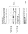
- FIG. 1 is a cross-sectional view of an exemplary laminated structure according to the prior art.
- Layer 5 is an antenna substrate that supports an antenna assembly and an integrated circuit unit 6 .
- Layer 4 is a bonding material used to adhere the antenna substrate to Layer 3 .
- Layer 3 is a white core PVC with heat seal coating HS-26 or similar seal coating.
- Layer 2 is a white core PVC front-side layer that can include print information.
- Layer 1 is a PVC overlay with a standard heat seal and/or protective coating. Between the antenna assembly/IC unit and the layers, air gaps 7 can form given the antenna and IC unit components and resultant non-uniformity of the antenna substrate.
- gaps or empty spaces
- the conductors e.g., antenna tracks
- thermal printing processes typically require an extremely flat surface to make uniform colors. If the surface is not flat, a blemish can be seen on a card after printing.
- the invention in one aspect, features a method of manufacturing an RFID structure.
- An antenna substrate is provided.
- a first stack layer is provided.
- An antenna assembly including an antenna track, and at least two contact pads, are formed on a first surface of the antenna substrate.
- An integrated circuit unit is coupled to the at least two contact pads.
- a first surface of the first stack layer, the first surface of the antenna substrate, or both are coated with a unidirectional thermally expansive coating material.
- the first surface of the antenna substrate is positioned to be adjacent to the first surface of the first stack layer.
- the invention in another aspect, features an RFID structure.
- the structure comprises an antenna substrate including, on a first surface, an antenna assembly having an antenna track and at least two contact pads.
- the structure also comprises an integrated circuit unit coupled to the at least two contact pads, a first stack layer positioned adjacent to the first surface of the antenna substrate, and an unheated unidirectional thermally expansive material separating the antenna substrate and the first stack layer, where gaps are defined between one or more portions of the antenna assembly and the thermally expansive material.
- the invention in another aspect, features an RFID structure.
- the structure comprises an antenna substrate including, on a first surface, an antenna assembly having an antenna track and at least two contact pads.
- the structure also comprises an integrated circuit unit coupled to the at least two contact pads, a first stack layer positioned adjacent to the first surface of the antenna substrate, and a previously heated unidirectional thermally expansive material separating the antenna substrate and the first stack layer, where gaps formed between the antenna substrate and the first stack layer are at least partially filled by the thermally expansive material.
- any of the above aspects can include one or more of the following features.
- a second stack layer is provided, a first surface of the second stack layer or a second surface of the antenna substrate opposite the first surface of the antenna substrate is coated with the thermally expansive coating material, and the first surface of the second stack layer is positioned to be adjacent to the second surface of the antenna substrate.
- a second antenna assembly including a second antenna track is formed on the second surface of the antenna substrate.
- the coating material is heated, where gaps formed by the antenna track or integrated circuit unit between the antenna substrate and the first stack layer before heating the coating material are at least 25% filled by thermal expansion of the coating material.
- a plurality of other antenna assemblies each including an antenna track, and at least two contact pads, are formed on the first surface of the antenna substrate, and integrated circuit units are coupled to the at least two contact pads on each of the plurality of other antenna assemblies.
- the coating material is heated, where gaps formed by the antenna tracks or integrated circuit units between the antenna substrate and the first stack layer before heating the coating material are at least 25% filled by thermal expansion of the coating material.
- the antenna assembly comprises etched copper, deposited copper, etched aluminum, deposited aluminum, etched gold, deposited gold, conductive pastes, conductive ink, conductive polymers, molybdenum, embedded copper, or any combination thereof.
- the antenna substrate comprises one or more non-conductive carrier materials including PET (polyester), FR-4 (or any other printed circuit board (PCB) material), PI (polyimide), BT (bismaleimide-triazine), PE (polyethylene), PVC (polyvinylchloride), PC (polycarbonate), PEN (polyethylene naphthalate), Teslin (silica-filled polyethylene), paper, or any combination thereof.
- the first stack layer comprises PET (polyester), PI (polyimide), BT (bismaleimide-triazine), PE (polyethylene), PVC (polyvinylchloride), PC (polycarbonate), PEN (polyethylene naphthalate), Teslin (silica-filled polyethylene), paper, or any combination thereof.
- the first stack layer and the antenna substrate are laminated between first and second laminate layers, and first and second overlay layers are provided to the first and second laminate layers.
- the first and second laminate layers comprise PET (polyester), PI (polyimide), BT (bismaleimide-triazine), PE (polyethylene), PVC (polyvinylchloride), PC (polycarbonate), PEN (polyethylene naphthalate), Teslin (silica-filled polyethylene), paper, or any combination thereof.
- visual display information is printed on the first overlay layer, the second overlay layer, or both the first and second overlay layers.
- the integrated circuit unit is positioned in a recess in the antenna substrate, in a recess in the first or second stack layer, or recesses in the antenna substrate, the first stack layer, and/or the second stack layer.
- the RFID structure comprises a RFID card component, a smartcard component, a ticket component, a passport component, a RFID label, a RFID sticker, a RFID poster, or any combination thereof.
- FIG. 1 is a cross-sectional view of an exemplary laminated structure according to the prior art.
- FIG. 2 is a cross-sectional view of an exemplary laminated structure according to an embodiment of the invention.
- FIG. 3 is a cross-sectional view of an exemplary laminated structure according to an embodiment of the invention.
- FIG. 4 is a cross-sectional view of an exemplary laminated structure according to an embodiment of the invention.
- FIG. 2 illustrates a cross-sectional view of an exemplary laminated structure 200 according to an embodiment of the invention.
- a prelaminate structure 202 (also called a prelam) includes the three center layers of the laminated structure 200 .
- the center layer 202 a , or core layer, of the prelam 202 includes the antenna assembly.
- the integrated circuit unit, or IC unit, (e.g., a chip) is typically buried in a recess in the center layer 204 a to protect it and to try and maintain a constant thickness of the prelam 202 surface.
- the laminated structure 200 (or stack) is put into a laminating machine which provides controlled temperature and/or pressure settings for a defined period of time(s) for the purpose of fusing the respective layers together and producing an integrated card.
- a laminating machine which provides controlled temperature and/or pressure settings for a defined period of time(s) for the purpose of fusing the respective layers together and producing an integrated card.
- the temperature profile as a function of time for the laminating machine can be controlled.
- the card layers can be constructed from PVC and similar plastics, because such materials melt before burning and, in some cases, additives can be included to change the characteristics of the card layers when heated. In this way, it is possible to create a material stack to melt within a range of temperatures and make the lamination of the card more controllable by having layers in the stack soften at different temperatures.
- the prelam 202 is manufactured by one company and then sold to another company for finishing into a card.
- prelams are laminated in sheet form and are not singulated until the outer layer(s) are put on by the second company.
- the outer layers can provide thickness and stiffness to the card as well as provide a support structure for graphics for such things as magnetic stripes and/or holograms.
- the final assembly can be accomplished using a laminating machine.
- the IC unit is partially protected from the large pressure of the laminating machine by being housed in its recess.
- the prelam 202 includes two outer sheets 204 b and 204 c that are coated with a unidirectional thermally expansive material.
- the unidirectional thermally expansive material expands and, in some embodiments, fills up the gaps/spaces that form between the layers of the prelam 202 , and also between the prelam 202 and the outer layers of the laminated structure.
- the temperature at which expansion of the materials is triggered can be selectable.
- the unidirectional thermally expansive material is cooled after it is heated, the material maintains its volume. In some embodiments, the volume of the material can decrease slightly (e.g., less than 5%).
- unidirectional refers to the characteristic of the material in which it does not return to its original volume upon cooling from a higher temperature.
- the material can create a strong bond with polyester and similar materials, from which etched inlays can be constructed.
- the unidirectional thermally expansive material is solid and forms part of the prelam 202 construction.
- the unidirectional thermally expansive material is benign and does not interfere with the operation of the prelam 202 (including the antenna assembly) and/or the final laminated card structure.
- the unidirectional thermally expansive coating material includes at least 60% of polyurethane polymers, at least 0.1% of acrylic copolymers, and at least 0.1% of hydrocarbons (e.g., isobutane and/or isopentane). In some embodiments, the unidirectional thermally expansive coating material includes 80-98% of polyurethane polymers and 20%-2% of acrylic copolymers and hydrocarbons.
- the polyurethane polymer can include aliphatic polyurethane surfactants free to formulate thermal activated adhesives.
- the polyurethane polymer can be in a waterborne dispersion.
- the tensile strength of the coating material can be 5 MPa and/or can include an elongation factor of 550-650%.
- the polyurethane polymer can include ESABOND DP 11 manufactured by Lamberti Chemical Specialties Co., Ltd. of Shanghai, China.
- the acrylic copolymers and hydrocarbons can include thermo-expandable microcapsules that encapsulate volatile hydrocarbons with acrylic copolymers.
- the average particle size of microcapsules can be between 6 and 12 ⁇ m.
- the chemical composition of the microcapsules can include a shell (acrylonitrile-copolymer) and a core (isobutene).
- expansion of the particles can begin at between 80° and 90° C.elsius and end expansion between 110° and 120° C.elsius.
- the coating material can be heated above the temperature trigger point for between 2 and 4 minutes.
- the acrylic copolymers and hydrocarbons can include Micropearl F-36 manufactured by Lehmann & Voss & Co. of Hamburg, Germany.
- the technology advantageously simplifies the production of chipcard structures, smartcard structures, passport structures, or other similar structures by increasing the quality with respect to the surface flatness/unevenness, decreasing the optical appearance of wires and/or IC units (e.g., chip or chip modules), eliminating the process of prelamination, using polyester inlays without cut out frame for the chip, and/or increasing the bond strength between materials (e.g., to polyester).
- IC units e.g., chip or chip modules
- FIG. 2 depicts a particular application of the unidirectional thermally expansive material
- the unidirectional thermally expansive material can be applied to any surface or combination of surfaces in the layers of the prelam 202 or the interior of laminated structure 200 .
- FIG. 3 is a cross-sectional view of an exemplary laminated structure 300 according to an embodiment of the invention.
- Layer 5 is an antenna substrate (e.g., polyester) that supports an antenna assembly and an integrated circuit unit 6 .
- Layer 5 is surrounded on all sides by Layer 4 .
- Layer 4 is the unidirectional thermally expansive material after it has been heated.
- Layer 3 is a white core PVC with heat seal coating HS-26X.
- Layer 2 is a white core PVC front-side layer that includes print information.
- Layer 1 is a PVC overlay with a standard heat seal coating.
- FIG. 4 is a cross-sectional view of an exemplary laminated structure 400 according to an embodiment of the invention.
- Layer 5 is an antenna substrate (e.g., polyester) that supports an antenna assembly and an integrated circuit unit 6 .
- Layer 5 is covered on its top and bottom surfaces by Layer 4 .
- Layer 4 is the unidirectional thermally expansive material after it has been heated.
- Layer 3 is a white core PVC with heat seal coating HS-26X.
- Layer 2 is a white core PVC front-side layer that includes print information.
- Layer 1 is a PVC overlay with a standard heat seal coating.
Abstract
Description
Claims (20)
Priority Applications (1)
| Application Number | Priority Date | Filing Date | Title |
|---|---|---|---|
| US13/858,582 US8851385B2 (en) | 2011-08-26 | 2013-04-08 | Card lamination |
Applications Claiming Priority (3)
| Application Number | Priority Date | Filing Date | Title |
|---|---|---|---|
| US201161527882P | 2011-08-26 | 2011-08-26 | |
| US201213594398A | 2012-08-24 | 2012-08-24 | |
| US13/858,582 US8851385B2 (en) | 2011-08-26 | 2013-04-08 | Card lamination |
Related Parent Applications (1)
| Application Number | Title | Priority Date | Filing Date |
|---|---|---|---|
| US201213594398A Continuation | 2011-08-26 | 2012-08-24 |
Publications (2)
| Publication Number | Publication Date |
|---|---|
| US20130240632A1 US20130240632A1 (en) | 2013-09-19 |
| US8851385B2 true US8851385B2 (en) | 2014-10-07 |
Family
ID=46982910
Family Applications (1)
| Application Number | Title | Priority Date | Filing Date |
|---|---|---|---|
| US13/858,582 Expired - Fee Related US8851385B2 (en) | 2011-08-26 | 2013-04-08 | Card lamination |
Country Status (5)
| Country | Link |
|---|---|
| US (1) | US8851385B2 (en) |
| EP (1) | EP2748771A1 (en) |
| CN (1) | CN103946873A (en) |
| RU (1) | RU2014111489A (en) |
| WO (1) | WO2013032921A1 (en) |
Cited By (2)
| Publication number | Priority date | Publication date | Assignee | Title |
|---|---|---|---|---|
| US20150298481A1 (en) * | 2012-11-29 | 2015-10-22 | Arjowiggins Security | Crease-resistant security film |
| US10023998B2 (en) | 2007-05-31 | 2018-07-17 | Ariowiggins Security | Crumple-resistant security sheet, a method of manufacturing such a sheet, and a security document including such a sheet |
Families Citing this family (4)
| Publication number | Priority date | Publication date | Assignee | Title |
|---|---|---|---|---|
| CN104377440A (en) * | 2014-11-01 | 2015-02-25 | 昆山联滔电子有限公司 | Novel antenna |
| CA2996147A1 (en) | 2015-08-20 | 2017-02-23 | Morphotrust Usa, Llc | Identification document with tactile feature |
| US20180309201A1 (en) * | 2015-10-14 | 2018-10-25 | Sivolam Marketing Ltd. | Systems and methods for multilayer antenna structure |
| US11445627B2 (en) | 2017-09-22 | 2022-09-13 | Shoei Printing Co., Ltd. | Resin card medium and manufacturing method therefor |
Citations (12)
| Publication number | Priority date | Publication date | Assignee | Title |
|---|---|---|---|---|
| DE19843425A1 (en) | 1998-09-22 | 2000-03-23 | Kunz Gmbh | Method for producing a contactless chip card |
| CN1258252A (en) | 1997-05-27 | 2000-06-28 | 三菱树脂株式会社 | Non-contact IC card and method for mfg. same |
| US20040155114A1 (en) * | 2001-03-22 | 2004-08-12 | Manfred Rietzler | Method for producing a contactless chip card and chip card produced according to said method |
| US20050040243A1 (en) * | 2001-12-24 | 2005-02-24 | Daoshen Bi | Contact smart cards having a document core, contactless smart cards including multi-layered structure, PET-based identification document, and methods of making same |
| US6923378B2 (en) * | 2000-12-22 | 2005-08-02 | Digimarc Id Systems | Identification card |
| US7147027B2 (en) * | 2001-04-06 | 2006-12-12 | Sony Corporation | Plate for hot pressing, hot press device, and card manufacturing device |
| US20070272760A1 (en) * | 2006-05-23 | 2007-11-29 | Axalto S.A. | Method for manufacturing a printed smart card with a visual relief effect |
| US20080265435A1 (en) * | 2007-04-30 | 2008-10-30 | International Business Machines Corporation | Structure and method for stress reduction in flip chip microelectronic packages using underfill materials with spatially varying properties |
| US20090250521A1 (en) * | 2005-11-16 | 2009-10-08 | Kyodo Printing Co., Ltd. | Non-contact type ic card |
| US20110031319A1 (en) * | 2009-08-05 | 2011-02-10 | Perfect Plastic Printing Corporation | RF Proximity Financial Transaction Card Having Metallic Foil Layer(s) |
| US20110267254A1 (en) * | 2008-09-25 | 2011-11-03 | Ksw Microtec Ag | Rfid transponder antenna |
| US20110266351A1 (en) * | 2008-11-03 | 2011-11-03 | Ksw Microtec Ag | Method for producing an rfid transponder product, and rfid transponder product produced using the method |
Family Cites Families (3)
| Publication number | Priority date | Publication date | Assignee | Title |
|---|---|---|---|---|
| DE19602821C1 (en) * | 1996-01-26 | 1997-06-26 | Siemens Ag | Method for producing a data card |
| US6191952B1 (en) * | 1998-04-28 | 2001-02-20 | International Business Machines Corporation | Compliant surface layer for flip-chip electronic packages and method for forming same |
| TWI457835B (en) * | 2004-02-04 | 2014-10-21 | Semiconductor Energy Lab | An article carrying a thin flim integrated circuit |
-
2012
- 2012-08-24 RU RU2014111489/08A patent/RU2014111489A/en not_active Application Discontinuation
- 2012-08-24 EP EP12769516.1A patent/EP2748771A1/en not_active Withdrawn
- 2012-08-24 CN CN201280050704.9A patent/CN103946873A/en active Pending
- 2012-08-24 WO PCT/US2012/052310 patent/WO2013032921A1/en active Application Filing
-
2013
- 2013-04-08 US US13/858,582 patent/US8851385B2/en not_active Expired - Fee Related
Patent Citations (13)
| Publication number | Priority date | Publication date | Assignee | Title |
|---|---|---|---|---|
| CN1258252A (en) | 1997-05-27 | 2000-06-28 | 三菱树脂株式会社 | Non-contact IC card and method for mfg. same |
| DE19843425A1 (en) | 1998-09-22 | 2000-03-23 | Kunz Gmbh | Method for producing a contactless chip card |
| US6923378B2 (en) * | 2000-12-22 | 2005-08-02 | Digimarc Id Systems | Identification card |
| US20040155114A1 (en) * | 2001-03-22 | 2004-08-12 | Manfred Rietzler | Method for producing a contactless chip card and chip card produced according to said method |
| US7147027B2 (en) * | 2001-04-06 | 2006-12-12 | Sony Corporation | Plate for hot pressing, hot press device, and card manufacturing device |
| US7823792B2 (en) * | 2001-12-24 | 2010-11-02 | L-1 Secure Credentialing, Inc. | Contact smart cards having a document core, contactless smart cards including multi-layered structure, PET-based identification document, and methods of making same |
| US20050040243A1 (en) * | 2001-12-24 | 2005-02-24 | Daoshen Bi | Contact smart cards having a document core, contactless smart cards including multi-layered structure, PET-based identification document, and methods of making same |
| US20090250521A1 (en) * | 2005-11-16 | 2009-10-08 | Kyodo Printing Co., Ltd. | Non-contact type ic card |
| US20070272760A1 (en) * | 2006-05-23 | 2007-11-29 | Axalto S.A. | Method for manufacturing a printed smart card with a visual relief effect |
| US20080265435A1 (en) * | 2007-04-30 | 2008-10-30 | International Business Machines Corporation | Structure and method for stress reduction in flip chip microelectronic packages using underfill materials with spatially varying properties |
| US20110267254A1 (en) * | 2008-09-25 | 2011-11-03 | Ksw Microtec Ag | Rfid transponder antenna |
| US20110266351A1 (en) * | 2008-11-03 | 2011-11-03 | Ksw Microtec Ag | Method for producing an rfid transponder product, and rfid transponder product produced using the method |
| US20110031319A1 (en) * | 2009-08-05 | 2011-02-10 | Perfect Plastic Printing Corporation | RF Proximity Financial Transaction Card Having Metallic Foil Layer(s) |
Non-Patent Citations (1)
| Title |
|---|
| International Search Report and Written Opinion from PCT patent application No. PCT/US2012/052310, issued Nov. 15, 2012, 12 pages. |
Cited By (3)
| Publication number | Priority date | Publication date | Assignee | Title |
|---|---|---|---|---|
| US10023998B2 (en) | 2007-05-31 | 2018-07-17 | Ariowiggins Security | Crumple-resistant security sheet, a method of manufacturing such a sheet, and a security document including such a sheet |
| US20150298481A1 (en) * | 2012-11-29 | 2015-10-22 | Arjowiggins Security | Crease-resistant security film |
| US9527332B2 (en) * | 2012-11-29 | 2016-12-27 | Arjowiggins Security | Crease-resistant security film |
Also Published As
| Publication number | Publication date |
|---|---|
| RU2014111489A (en) | 2015-10-10 |
| EP2748771A1 (en) | 2014-07-02 |
| CN103946873A (en) | 2014-07-23 |
| WO2013032921A1 (en) | 2013-03-07 |
| US20130240632A1 (en) | 2013-09-19 |
Similar Documents
| Publication | Publication Date | Title |
|---|---|---|
| US8851385B2 (en) | Card lamination | |
| US8955759B2 (en) | Inlays for security documents | |
| KR100998605B1 (en) | Method of manufacturing a contactless or a contact/contactless hybrid chip card with enhanced evenness | |
| EP1914671B1 (en) | Transponder embedded in a flexible multi-layer support | |
| AU776169B2 (en) | Method for making a non-contact smart card with an antenna support made of fibrous material | |
| JP2008537215A (en) | A method of manufacturing a modern smart card with integrated electronics using an isotropic thermoset adhesive material having a high quality outer surface. | |
| CN104471594A (en) | Information carrying card comprising a cross-linked polymer composition, and method of making the same | |
| CN104769612B (en) | Information including crosslinking polymer composition carries card and preparation method thereof | |
| JP2004533947A (en) | Injection molded product and method of manufacturing the same | |
| US20150186768A1 (en) | Transparent rfid antenna | |
| EP1842689B1 (en) | Thermally stable proximity indentifaction card | |
| EP2490157A2 (en) | Reversible thermosensitive recording medium and method for producing the same | |
| JP4676196B2 (en) | RFID tag | |
| US20120038141A1 (en) | Method for manufacturing a functional laminate, functional laminate and its use for security documents | |
| CN101730624A (en) | Smart information carrier and production process therefor | |
| CN111126541A (en) | Structure of RFID smart card and manufacturing method thereof | |
| JP4930758B2 (en) | Non-contact type data carrier device and manufacturing method thereof | |
| US20140234577A1 (en) | Plastic Card Prelaminate and Plastic Card Including a Phone Sticker | |
| JP2003067706A (en) | Non-contact ic card recording medium and its manufacturing method | |
| EP3968229A1 (en) | Method for manufacturing contactless smart card made from recycled material having low melting point and resulting smart card | |
| JP5375648B2 (en) | Non-contact IC label | |
| JP2023174413A (en) | laminate | |
| JP2009009452A (en) | Rewrite rfid medium and manufacturing method thereof | |
| JP2022148016A (en) | IC card | |
| CN201352356Y (en) | Electronic identification tape |
Legal Events
| Date | Code | Title | Description |
|---|---|---|---|
| AS | Assignment |
Owner name: IDENTIVE GROUP, INC., CALIFORNIA Free format text: ASSIGNMENT OF ASSIGNORS INTEREST;ASSIGNORS:VOGT, WERNER;LOOSER, ANDREAS;LOOSER, CHRISITIAN;AND OTHERS;SIGNING DATES FROM 20130408 TO 20130430;REEL/FRAME:030539/0780 |
|
| AS | Assignment |
Owner name: OPUS BANK, CALIFORNIA Free format text: SECURITY INTEREST;ASSIGNORS:IDENTIVE GROUP, INC.;HIRSCH ELECTRONICS LLC;IDONDEMAND, INC.;REEL/FRAME:032591/0166 Effective date: 20140331 |
|
| AS | Assignment |
Owner name: EAST WEST BANK, CALIFORNIA Free format text: SECURITY INTEREST;ASSIGNOR:IDENTIV, INC.;REEL/FRAME:041216/0761 Effective date: 20170208 |
|
| AS | Assignment |
Owner name: IDENTIV, INC., CALIFORNIA Free format text: RELEASE BY SECURED PARTY;ASSIGNOR:OPUS BANK;REEL/FRAME:041243/0877 Effective date: 20170210 Owner name: IDONDEMAND INC., CALIFORNIA Free format text: RELEASE BY SECURED PARTY;ASSIGNOR:OPUS BANK;REEL/FRAME:041243/0877 Effective date: 20170210 Owner name: HIRSCH ELECTRONICS LLC, CALIFORNIA Free format text: RELEASE BY SECURED PARTY;ASSIGNOR:OPUS BANK;REEL/FRAME:041243/0877 Effective date: 20170210 |
|
| FEPP | Fee payment procedure |
Free format text: MAINTENANCE FEE REMINDER MAILED (ORIGINAL EVENT CODE: REM.) |
|
| LAPS | Lapse for failure to pay maintenance fees |
Free format text: PATENT EXPIRED FOR FAILURE TO PAY MAINTENANCE FEES (ORIGINAL EVENT CODE: EXP.); ENTITY STATUS OF PATENT OWNER: SMALL ENTITY |
|
| STCH | Information on status: patent discontinuation |
Free format text: PATENT EXPIRED DUE TO NONPAYMENT OF MAINTENANCE FEES UNDER 37 CFR 1.362 |
|
| FP | Lapsed due to failure to pay maintenance fee |
Effective date: 20181007 |