US8832500B2 - Multiple clock domain tracing - Google Patents
Multiple clock domain tracing Download PDFInfo
- Publication number
- US8832500B2 US8832500B2 US13/572,249 US201213572249A US8832500B2 US 8832500 B2 US8832500 B2 US 8832500B2 US 201213572249 A US201213572249 A US 201213572249A US 8832500 B2 US8832500 B2 US 8832500B2
- Authority
- US
- United States
- Prior art keywords
- clock signal
- data
- time stamp
- input
- granularity
- Prior art date
- Legal status (The legal status is an assumption and is not a legal conclusion. Google has not performed a legal analysis and makes no representation as to the accuracy of the status listed.)
- Active, expires
Links
Images


Classifications
-
- G—PHYSICS
- G06—COMPUTING; CALCULATING OR COUNTING
- G06F—ELECTRIC DIGITAL DATA PROCESSING
- G06F11/00—Error detection; Error correction; Monitoring
- G06F11/36—Preventing errors by testing or debugging software
- G06F11/362—Software debugging
- G06F11/3648—Software debugging using additional hardware
- G06F11/3656—Software debugging using additional hardware using a specific debug interface
-
- G—PHYSICS
- G06—COMPUTING; CALCULATING OR COUNTING
- G06F—ELECTRIC DIGITAL DATA PROCESSING
- G06F1/00—Details not covered by groups G06F3/00 - G06F13/00 and G06F21/00
- G06F1/04—Generating or distributing clock signals or signals derived directly therefrom
- G06F1/10—Distribution of clock signals, e.g. skew
-
- G—PHYSICS
- G06—COMPUTING; CALCULATING OR COUNTING
- G06F—ELECTRIC DIGITAL DATA PROCESSING
- G06F1/00—Details not covered by groups G06F3/00 - G06F13/00 and G06F21/00
- G06F1/04—Generating or distributing clock signals or signals derived directly therefrom
- G06F1/14—Time supervision arrangements, e.g. real time clock
-
- G—PHYSICS
- G06—COMPUTING; CALCULATING OR COUNTING
- G06F—ELECTRIC DIGITAL DATA PROCESSING
- G06F11/00—Error detection; Error correction; Monitoring
- G06F11/36—Preventing errors by testing or debugging software
- G06F11/362—Software debugging
- G06F11/3636—Software debugging by tracing the execution of the program
Definitions
- This disclosure relates generally to data processors, and more specifically to data processors capable of storing trace data.
- SoCs systems on chips
- modules such as central processing units (“CPUs”), advanced processing units (“APUs”), graphics processing units (“GPUs”), memory sub-systems, system controllers, and complex peripheral functions.
- CPUs central processing units
- APUs advanced processing units
- GPUs graphics processing units
- memory sub-systems system controllers
- complex peripheral functions such as gaining visibility into the operation of the system and determining that the system is operating as desired.
- the complexity and cost of finding and eliminating functional “bugs” provide significant challenges.
- generating, storing, and analyzing the data required to determine if the defects are generally within the system, within a specific module, or between a set of modules present a significant challenge.
- FIG. 1 illustrates in block diagram form a microprocessor with tracing capability known in the prior art.
- FIG. 2 illustrates in block diagram form a portion of another microprocessor with tracing capability known in the prior art.
- FIG. 3 illustrates in block diagram form an integrated circuit with tracing capability according to some embodiments.
- FIG. 4 illustrates a flow chart of a method for tracing according to some embodiments.
- FIG. 1 illustrates in block diagram form a microprocessor 100 with tracing capability known in the prior art.
- Microprocessor 100 generally includes a CPU core 110 , a trace generation unit 120 , and a trace buffer 140 .
- Trace generation unit 120 includes interface logic 122 , a test access port (“TAP”) controller 124 , a functional block 126 labeled “TRIGGER, SEQUENCER, AND COUNTERS”, and a trace packet generator 130 .
- Trace packet generator 130 includes a trace control 132 and a first-in, first-out buffer (“FIFO”) 134 .
- FIFO first-in, first-out buffer
- CPU core 110 transmits and receives a variety of signals relevant to its operational state that are externally visible, such as addresses, data, control signals, interrupt and exception signals, and the like.
- Interface logic 122 has an input for receiving selected signals from CPU core 110 , and an output.
- TAP controller 124 has a bidirectional port for transmitting and receiving a set of input and/or output signals, and provides various control signals, not shown in FIG. 1 , to configure and control the operation of trace generation unit 120 .
- Functional block 126 has an input connected to the output of interface logic 122 , and an output for providing an enable signal labeled “TRACE ENABLE”.
- Trace packet generator 130 has an input connected to the output of interface logic 122 , and an output for providing trace packets.
- Trace buffer 140 has an input connected to the output of trace packet generator 130 .
- CPU core 110 executes instructions corresponding to one or more programs.
- CPU core 110 also provides a debug data stream that includes debug data that is generated by CPU core 110 while executing (or as a result of executing) instructions corresponding to one or more programs.
- Trace generation unit 120 handles interfacing and communication with CPU core 110 , system test, and starting and stopping the generation of debug records.
- interface logic 122 manages communications between the receive circuits and transmit circuits of CPU core 110 and trace generation unit 120 .
- Interface logic 122 provides triggers to functional block 126 and also provides a debug data stream received from CPU CORE 110 to trace packet generator 130 .
- TAP controller 124 defines a common boundary scan test interface, to support the operation of on-chip and off-chip system testing.
- an internal state machine drives the operation of TAP controller 124 .
- Instruction registers define the system-level testing protocol and data registers store the data structures under test by TAP controller 124 .
- TAP controller 124 controls the operation of trace generation unit 120 by providing test clocks for synchronizing the internal state machine, test data input and test data output for exchanging debug data between functional units and system test logic, and a reset signal for initializing the internal state machine of TAP controller 124 .
- Functional block 126 initiates tracing in response to triggers and controls complex sequences and state changes of tracing operations as defined by certain trigger inputs and the tracing protocol. Also, functional block 126 provides counters for counting events.
- Trace packet generator 130 stores information from CPU core 110 in response to an activation of TRACE ENABLE. This information includes values of input/output (“I/O”) signals, routing signal values, debug data, and the like. Also trace generation unit 120 stores debug data as a function of a specific configuration and a specific operating mode of CPU core 110 .
- I/O input/output
- trace generation unit 120 stores debug data as a function of a specific configuration and a specific operating mode of CPU core 110 .
- trace control 132 generates control signals to manage starting and stopping of trace packet generator 130 and to select the operation protocol of trace packet generator 130 .
- FIFO 134 collects and organizes debug data, by storing the debug data in the order the debug data was received. Likewise, FIFO 134 provides the debug data to trace buffer 140 in the order the debug data was received.
- Trace buffer 140 stores the debug data, including data that represents certain activities of CPU core 110 , and data that includes other system information gathered during tracing. System resources access trace buffer 140 to analyze the debug data.
- trace generation unit 120 and trace buffer 140 are dedicated to CPU core 110 , they can be located physically close to CPU core 110 on a common integrated circuit die. Trace generation unit 120 , trace buffer 140 , and CPU core 110 also operate within a single clock domain. In this example they are capable of performing adequate tracing of microprocessor 100 . However as the complexity and size of CPU core 110 increase, and microprocessor 100 is expanded to include multiple modules such as other CPUs or sub-portions of a CPU, GPUs, and the like with tracing capability located in remote parts of microprocessor 100 and having their own separate clock domains, trace generation unit 120 becomes insufficient to generate adequate trace data.
- FIG. 2 illustrates in block diagram form a portion of another microprocessor 200 with tracing capability known in the prior art.
- Microprocessor 200 generally includes a clock generator 210 , a circuit 220 labeled “CIRCUIT 1”, a circuit 230 labeled “CIRCUIT 2”, a multiplexor 240 , a trace cache buffer 250 , and a debug controller 260 .
- Clock generator 210 has an output connected to an input of circuit 220 for providing a clock signal labeled “CLK1”, an output connected to an input of circuit 230 for providing a clock signal labeled “CLK2”, and an output connected to an input terminal of trace cache buffer 250 for providing a signal labeled “TRACE CLOCK”.
- Circuit 220 has an output connected to an input of multiplexor 240 over a bus labeled “DATA1”.
- Circuit 230 has an output connected to an input of multiplexor 240 over a bus labeled “DATA2”.
- Multiplexor 240 has an input connected to an output of debug controller 260 for receiving a signal labeled “SELECT” and an output connected to an input of trace cache buffer 250 over a bus.
- Trace cache buffer 250 has an input connected to an output of debug controller 260 for receiving a signal labeled “ENABLE”, an input for receiving the TRACE CLOCK, and an output for providing trace data.
- Debug controller 260 has an input for receiving a set of signals labeled “TRIGGERS”.
- clock generator 210 provides clock signal CLK1 to circuit 220 , and clock signal CLK2 to circuit 230 . Also, clock generator 210 provides clock signal TRACE CLOCK to trace cache buffer 250 and debug controller 260 . Circuit 220 executes local logic functions based on timing edges provided by clock signal CLK1. In response, circuit 220 provides DATA1, where DATA1 includes debug data that reflect results of the activity of circuit 220 .
- circuit 230 executes local logic functions based on timing edges provided by clock signal CLK2. In response, circuit 230 provides DATA2, where DATA2 includes debug data that reflect results of the activity of circuit 230 . Circuit 220 and circuit 230 each initiate internal tracing sequences and each circuit controls the state changes of tracing operations as defined by certain trigger inputs and the tracing protocol.
- debug controller 260 In response to system TRIGGERS, debug controller 260 generates signal ENABLE to manage when trace cache buffer 250 collects trace records. Also, debug controller 260 provides signal SELECT to instruct multiplexor 240 when to provide either DATA1 or DATA2 to trace cache buffer 250 .
- Trace cache buffer 250 stores debug data, including data that represents certain activities of circuit 220 and circuit 230 , such as certain values of input/output (“I/O”) signals, routing signal values, debug data values, and the like. Trace cache buffer 250 stores each trace entry synchronous with timing edges provided by the TRACE CLOCK. System resources access trace cache buffer 250 to analyze the debug data.
- debug data including data that represents certain activities of circuit 220 and circuit 230 , such as certain values of input/output (“I/O”) signals, routing signal values, debug data values, and the like.
- Trace cache buffer 250 stores each trace entry synchronous with timing edges provided by the TRACE CLOCK. System resources access trace cache buffer 250 to analyze the debug data.
- microprocessor 200 captures traces synchronously with clock signal TRACE CLOCK
- data may arrive at the input to trace cache buffer 250 in an unknown phase with respect to its own clock.
- clock signal TRACE CLOCK it may be possible to generate clock signal TRACE CLOCK in a way to ensure that the data is captured properly.
- the skew between clock signal CLK1 or clock signal CLK2 and clock signal TRACE CLOCK is unknown, and at certain points in time, trace cache buffer 250 may capture erroneous trace data while it is making a transition.
- trace cache buffer 250 can store data from only one source at a time, whereas information from both circuit 220 and circuit 230 may be relevant to debugging the operation of microprocessor 200 .
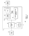
- FIG. 3 illustrates in block diagram form an integrated circuit 300 with tracing capability according to some embodiments.
- Integrated circuit 300 generally includes a functional block 310 and a debug module 320 .
- Functional block 310 includes a circuit 312 labeled “CIRCUIT 1” and a circuit 314 labeled “CIRCUIT 2”.
- Debug module 320 includes a global time stamp counter (“TSC”) 330 , a functional block 340 , a functional block 350 , a trace cache buffer 360 , and a debug state machine (“DSM”) 370 .
- TSC 330 has an input for receiving a clock labeled “REFCLK” and an output connected to an input port of a synchronization (“SYNC”) latch 346 for conducting a set of least significant bits labeled “N LSBs”.
- SYNC synchronization
- Functional block 340 includes a granularity counter 342 , a SYNC latch 344 , and a SYNC latch 346 .
- Granularity counter 342 has an input connected to an output of circuit 312 for receiving a signal labeled “CLK1” and an input labeled “RST” connected to an output of SYNC latch 344 for receiving a reset signal.
- SYNC latch 344 has an input for receiving REFCLK, and an input for receiving CLK1.
- SYNC latch 346 has an input for receiving CLK1.
- Functional block 350 includes a granularity counter 352 , a SYNC latch 354 , and a SYNC latch 356 .
- Granularity counter 352 has an input connected to an output of circuit 314 for receiving a signal labeled “CLKN” and an input labeled “RST” connected to an output of SYNC latch 354 for receiving a reset signal.
- SYNC latch 354 has an input for receiving REFCLK, and an input for receiving CLKN.
- SYNC latch 356 has an input port for receiving the N LSBs of the global time stamp, and an input for receiving CLKN.
- Trace cache buffer 360 includes a partition 362 , a partition 364 , a SYNC latch 366 , and a SYNC latch 368 .
- Partition 362 includes a number of storage locations for storing trace records, each having fields labeled “GLOBAL TSC”, “SS_CLKCnt”, and “DATA”.
- the GLOBAL TSC fields have an input port connected to an output of SYNC latch 346 .
- the SS_CLKCnt fields have an input connected to an output of granularity counter 342 .
- the DATA fields have an input connected to an output of circuit 312 for receiving DATA1.
- Partition 362 has an output for providing an output labeled “TRACE DATA OUT”.
- Partition 364 includes a number of storage locations for storing trace records each having fields labeled “GLOBAL TSC”, “SS_CLKCnt”, and “DATA”.
- the GLOBAL TSC fields have an input connected to an output of SYNC latch 356 over a bus.
- the SS_CLKCnt fields have an input connected to an output of granularity counter 352 .
- the DATA fields have an input connected to an output of circuit 314 for receiving DATAN.
- Partition 364 has an input connected to an output of SYNC latch 368 and output for providing TRACE DATA OUT.
- SYNC latch 366 has an input connected to an output of DSM 370 for receiving a signal labeled “DbgWrEn1” and an input for receiving a trigger signal labeled “TCLK”.
- SYNC latch 368 has an input connected to an output of DSM 370 for receiving a signal labeled “DbgWrEnN” and an input for receiving TCLK.
- functional block 310 includes a certain number of circuit blocks, such as representative circuits 312 and 314 .
- Each circuit provides a source synchronous data stream.
- Each one of the source synchronous data streams includes a clock signal and corresponding data.
- a circuit sources the associated clock signal to provide a tight timing reference for the associated data.
- each circuit, including circuit 312 and circuit 314 generally sources a clock that is asynchronous to all other source synchronous clocks.
- circuit 312 provides a source synchronous clock CLK1 and associated source synchronous DATA1. Also, circuit 314 provides a source synchronous CLKN, and associated source synchronous DATAN.
- a global clock source provides a global reference clock REFCLK, and global TSC 330 counts pulses of REFCLK to form a global time stamp including a certain number of least significant bits (N LSBs). REFCLK is lower in frequency than CLK1 or CLKN by a ratio of 1:2 or less.
- granularity counter 342 counts pulses of CLK1 to provide a granularity count to the SS_CLKCnt field of the selected record in partition 362 .
- SYNC latch 344 synchronizes REFCLK with CLK1 to reset granularity counter 342 . Since REFCLK is asynchronous to CLK1, SYNC latch 344 provides a stable glitch-free transfer of REFCLK to the RST input of granularity counter 342 .
- the value in granularity counter 342 is stored as a portion of a trace record in the SS_CLKCnt location of the selected record of partition 362 .
- This trace record portion includes both a coarse, global time stamp and a finer granularity time stamp, to allow better correlation of traces between circuit 312 and circuit 314 .
- SYNC latch 346 synchronizes the N LSBs of global TSC 330 with CLK1 to provide a synchronized global time stamp value.
- Partition 362 stores this value in location GLOBAL TSC (N LSBs) of the selected record of partition 362 .
- granularity counter 352 counts pulses of CLKN to provide a granularity count to location SS_CLKCnt of the selected record of partition 364 .
- SYNC latch 354 synchronizes REFCLK with CLKN to reset granularity counter 352 . Since REFCLK is asynchronous to CLKN, SYNC latch 354 provides a stable glitch-free transfer of REFCLK to the RST input of granularity counter 352 .
- the value in granularity counter 352 is stored as a portion of a trace record in the SS_CLKCnt field of the selected trace record of partition 364 .
- This field represents the relationship between the CLKN clock frequency and the REFCLK clock frequency.
- SYNC latch 356 synchronizes the N LSBs output of global TSC 330 with CLKN to provide a synchronized global time stamp value.
- Partition 364 stores this value in the GLOBAL TSC field of the selected record of the selected record of partition 364 .
- trace cache buffer 360 stores DATA1 synchronous with CLK1 in the DATA field in partition 362 and DATAN synchronous with CLKN in the DATA field in partition 364 .
- DSM 370 provides a central location for the control of tracing and debug operations of integrated circuit 300 . Also, DSM 370 enables the storing of a source synchronous data stream, filters the rules that define how trace records are stored, starts and stops clocks that synchronize and store trace records, and provides a system debug mode interrupt based on certain results of the trace records.
- certain registers store and provide TRIGGERS, or a sequence of TRIGGERS, over a bus to DSM 370 .
- functional blocks such as CPUs, APUs, GPUs, memory sub-systems, system controllers, and complex peripheral functions, provide discrete TRIGGERS, or a sequence of discrete TRIGGERS, to DSM 370 .
- Functional block 310 provides source synchronous data streams to debug module 320 that each represent the operation of circuits within functional block 310 , including circuit 312 and circuit 314 .
- DSM 370 responds to selected TRIGGERS by providing selected enabling signals that include “DbgWrEn1” and “DbgWrEnN” to trace cache buffer 360 . Enabled by the selected enabling signals, trace cache buffer 360 stores the trace records and provides TRACE DATA OUT to system resources, not shown in FIG. 3 .
- DSM 370 provides enable signal DbgWrEn1 to SYNC latch 366 .
- SYNC latch 366 synchronizes DbgWrEn1 to clock signal TCLK.
- SYNC latch 366 further enables storing of an associated trace record, for a given rising edge of CLK1, in the selected location of partition 362 .
- Partition 362 includes separate locations for the synchronized global time stamp, the synchronized granularity count, and the synchronized source synchronous data stream, DATA1.
- the data record includes a corresponding timestamp value (including both a coarse, global time stamp and a finer granularity local time stamp) to provide correlation of the data in each location to a time value.
- SYNC latch 368 synchronizes DbgWrEnN to TCLK.
- SYNC latch 368 further enables storing of an associated trace record, for a given rising edge of CLKN, in the corresponding location of partition 364 .
- Partition 364 includes separate locations for the synchronized global time stamp, the synchronized granularity count, and the synchronized source synchronous data stream, DATAN.
- the record includes a corresponding timestamp value to provide correlation of the data in each location to a time value.
- debug module 320 By storing both a coarse, global time stamp and a fine local time stamp, debug module 320 allows the correlation of trace records from multiple circuits even though their own clocks have random phase and frequency with respect to each other. In addition, debug module 320 allows simultaneous storage of multiple trace data streams, which allow more sophisticated debug by storing data from multiple, interrelated functional circuits in response to a single trigger.
- FIG. 4 illustrates a flow chart of a method 400 for tracing according to some embodiments.
- Action box 410 includes receiving a first source synchronous data stream comprising a first clock signal and first data.
- Action box 412 includes receiving a second source synchronous data stream comprising a second clock signal and second data.
- Action box 420 includes counting pulses of a reference clock signal to form a global time stamp.
- Action box 430 includes counting pulses of the first clock signal to form a first granularity count. In some embodiments, this counting includes resetting the first granularity count in response to transitions of the reference clock signal.
- Action box 432 includes counting pulses of the second clock signal to form a second granularity count.
- this counting includes resetting the second granularity count in response to transitions of the reference clock signal.
- Action box 440 includes storing in a first partition of a trace cache buffer the global time stamp, the first granularity count, and the first data in response to a first enable signal. In some embodiments, this storing includes synchronizing the first enable signal to a third clock signal to provide a synchronized first enable signal, and storing in the first partition of the trace cache buffer the global time stamp, the first granularity count, and the first data in response to the synchronized first enable signal.
- Action box 442 includes storing in a second partition of the trace cache buffer the global time stamp, the second granularity count, and the second data in response to a second enable signal.
- this storing includes synchronizing the second enable signal to the third clock signal to provide a synchronized second enable signal, and storing in the second partition of the trace cache buffer the global time stamp, the second granularity count, and the second data in response to the synchronized second enable signal.
- method 400 further includes an action box 450 including outputting data from a selected one of the first and second partitions of the trace cache buffer, an action box 460 including latching the global time stamp in response to the first clock signal to provide a first latched global time stamp, and/or an action box 470 including selectively providing the first and second enable signals in response to a plurality of triggers.
- action box 450 including outputting data from a selected one of the first and second partitions of the trace cache buffer
- an action box 460 including latching the global time stamp in response to the first clock signal to provide a first latched global time stamp
- an action box 470 including selectively providing the first and second enable signals in response to a plurality of triggers.
- the actions of method 400 may also be implemented in different orders or in different combinations in various embodiments.
- the tracing functions of the integrated circuit of FIG. 3 may be implemented with various combinations of hardware and software, and the software component may be stored in a computer readable storage medium for execution by at least one processor. Moreover the method illustrated in FIG. 4 may also be governed by instructions that are stored in a computer readable storage medium and that are executed by at least one processor. Each of the operations shown in FIG. 4 may correspond to instructions stored in a non-transitory computer memory or computer readable storage medium.
- the non-transitory computer readable storage medium includes a magnetic or optical disk storage device, solid state storage devices such as Flash memory, or other non-volatile memory device or devices.
- the computer readable instructions stored on the non-transitory computer readable storage medium may be in source code, assembly language code, object code, or other instruction format that is interpreted and/or executable by one or more processors.
- integrated circuit 300 may be described or represented by a computer accessible data structure in the form of a database or other data structure which can be read by a program and used, directly or indirectly, to fabricate integrated circuit 300 .
- this data structure may be a behavioral-level description or register-transfer level (RTL) description of the hardware functionality in a high level design language (HDL) such as Verilog or VHDL.
- HDL high level design language
- the description may be read by a synthesis tool which may synthesize the description to produce a netlist comprising a list of gates from a synthesis library.
- the netlist comprises a set of gates which also represent the functionality of the hardware comprising integrated circuit 300 .
- the netlist may then be placed and routed to produce a data set describing geometric shapes to be applied to masks.
- the masks may then be used in various semiconductor fabrication steps to produce a integrated circuit 300 .
- the database on the computer accessible storage medium may be the netlist (with or without the synthesis library) or the data set, as desired, or Graphic Data System (GDS) II data.
- GDS Graphic Data System
- the traced circuits in functional block 310 can be formed by a variety of elements including a GPU, a CPU core, an APU, a memory sub-system, a system controller (a “north bridge” or a “south bridge”), complex peripheral functions, and so on, and sub-circuits of each of them.
- integrated circuit 300 could include a certain number of functional blocks, where a functional block could include a certain set of GPUs, CPU cores, APUs, memory sub-systems, system controllers, complex peripheral functions, and so on.
- functional block 310 could include a CPU core, an APU, and a Universal Serial Bus (“USB”) controller, and another functional block could include a memory sub-system and a bus arbitration module.
- USB Universal Serial Bus
- functional block 310 of integrated circuit 300 provides CLK1 and CLKN to debug module 320 , and the system provides a REFCLK to debug module 320 having a frequency of 1:2 or less with respect to the lowest operating frequency of each of CLK1 and CLKN, but the precise ratio used could vary in different embodiments. Also, CLK1 and CLKN could run at faster or slower frequencies with respect to each other, and could be substantially asynchronous to each other.
- partition 362 and partition 364 include three separate fields, namely GLOBAL TSC, SS_CLKCnt, and DATA, but any number of fields could be implemented in any number of ways, and any one of these fields could store other selected data using the higher or lower frequency CLK1 or CLKN clocks.
- the illustrated embodiment shows SYNC latch 344 , SYNC latch 346 , SYNC latch 354 , and SYNC latch 356 , but debug module 320 could bypass one or more of these synchronization latches depending on a particular relationship between CLK1, CLKN, and REFCLK.
Abstract
Description
Claims (24)
Priority Applications (1)
| Application Number | Priority Date | Filing Date | Title |
|---|---|---|---|
| US13/572,249 US8832500B2 (en) | 2012-08-10 | 2012-08-10 | Multiple clock domain tracing |
Applications Claiming Priority (1)
| Application Number | Priority Date | Filing Date | Title |
|---|---|---|---|
| US13/572,249 US8832500B2 (en) | 2012-08-10 | 2012-08-10 | Multiple clock domain tracing |
Publications (2)
| Publication Number | Publication Date |
|---|---|
| US20140047262A1 US20140047262A1 (en) | 2014-02-13 |
| US8832500B2 true US8832500B2 (en) | 2014-09-09 |
Family
ID=50067128
Family Applications (1)
| Application Number | Title | Priority Date | Filing Date |
|---|---|---|---|
| US13/572,249 Active 2033-01-31 US8832500B2 (en) | 2012-08-10 | 2012-08-10 | Multiple clock domain tracing |
Country Status (1)
| Country | Link |
|---|---|
| US (1) | US8832500B2 (en) |
Cited By (2)
| Publication number | Priority date | Publication date | Assignee | Title |
|---|---|---|---|---|
| US20160232046A1 (en) * | 2013-09-27 | 2016-08-11 | Fts Computertechnik Gmbh | Method for detecting a failure of a constituent system in a system-of-systems |
| US20180225063A1 (en) * | 2017-02-08 | 2018-08-09 | Intel IP Corporation | Device, system and method to provide categorized trace information |
Families Citing this family (3)
| Publication number | Priority date | Publication date | Assignee | Title |
|---|---|---|---|---|
| US9910475B2 (en) * | 2014-12-23 | 2018-03-06 | Intel Corporation | Processor core power event tracing |
| US10691576B1 (en) * | 2017-09-26 | 2020-06-23 | Amazon Technologies, Inc. | Multiple reset types in a system |
| US20220198110A1 (en) * | 2020-12-23 | 2022-06-23 | Intel Corporation | Debugging architecture for system in package composed of multiple semiconductor chips |
Citations (70)
| Publication number | Priority date | Publication date | Assignee | Title |
|---|---|---|---|---|
| US3896419A (en) | 1974-01-17 | 1975-07-22 | Honeywell Inf Systems | Cache memory store in a processor of a data processing system |
| US5210843A (en) | 1988-03-25 | 1993-05-11 | Northern Telecom Limited | Pseudo set-associative memory caching arrangement |
| US5381533A (en) | 1992-02-27 | 1995-01-10 | Intel Corporation | Dynamic flow instruction cache memory organized around trace segments independent of virtual address line |
| US5563594A (en) | 1994-08-31 | 1996-10-08 | Motorola | Circuit and method of timing data transfers |
| US5669003A (en) | 1994-12-23 | 1997-09-16 | Intel Corporation | Method of monitoring system bus traffic by a CPU operating with reduced power |
| US5764885A (en) | 1994-12-19 | 1998-06-09 | Digital Equipment Corporation | Apparatus and method for tracing data flows in high-speed computer systems |
| US5787095A (en) | 1994-10-25 | 1998-07-28 | Pyramid Technology Corporation | Multiprocessor computer backlane bus |
| US5881261A (en) | 1996-01-26 | 1999-03-09 | Advanced Micro Devices, Inc. | Processing system that rapidly indentifies first or second operations of selected types for execution |
| US5896528A (en) | 1995-03-03 | 1999-04-20 | Fujitsu Limited | Superscalar processor with multiple register windows and speculative return address generation |
| US5930497A (en) | 1997-12-11 | 1999-07-27 | International Business Machines Corporation | Method and means for generation of realistic access patterns in storage subsystem benchmarking and other tests |
| US5944841A (en) | 1997-04-15 | 1999-08-31 | Advanced Micro Devices, Inc. | Microprocessor with built-in instruction tracing capability |
| EP0957428A2 (en) | 1998-05-12 | 1999-11-17 | International Business Machines Corporation | Method and apparatus for fetching noncontiguous instructions in a data processing system |
| US6014742A (en) | 1997-12-31 | 2000-01-11 | Intel Corporation | Trace branch prediction unit |
| US6167536A (en) | 1997-04-08 | 2000-12-26 | Advanced Micro Devices, Inc. | Trace cache for a microprocessor-based device |
| US6185675B1 (en) | 1997-10-24 | 2001-02-06 | Advanced Micro Devices, Inc. | Basic block oriented trace cache utilizing a basic block sequence buffer to indicate program order of cached basic blocks |
| US6195744B1 (en) | 1995-10-06 | 2001-02-27 | Advanced Micro Devices, Inc. | Unified multi-function operation scheduler for out-of-order execution in a superscaler processor |
| US6205508B1 (en) | 1999-02-16 | 2001-03-20 | Advanced Micro Devices, Inc. | Method for distributing interrupts in a multi-processor system |
| US6212628B1 (en) | 1998-04-09 | 2001-04-03 | Teranex, Inc. | Mesh connected computer |
| US6216206B1 (en) | 1997-12-16 | 2001-04-10 | Intel Corporation | Trace victim cache |
| US6233678B1 (en) | 1998-11-05 | 2001-05-15 | Hewlett-Packard Company | Method and apparatus for profiling of non-instrumented programs and dynamic processing of profile data |
| US6247121B1 (en) | 1997-12-16 | 2001-06-12 | Intel Corporation | Multithreading processor with thread predictor |
| US6256728B1 (en) | 1997-11-17 | 2001-07-03 | Advanced Micro Devices, Inc. | Processor configured to selectively cancel instructions from its pipeline responsive to a predicted-taken short forward branch instruction |
| US6298394B1 (en) | 1999-10-01 | 2001-10-02 | Stmicroelectronics, Ltd. | System and method for capturing information on an interconnect in an integrated circuit |
| US6311296B1 (en) | 1998-12-29 | 2001-10-30 | Intel Corporation | Bus management card for use in a system for bus monitoring |
| US6321290B1 (en) | 1998-04-28 | 2001-11-20 | Nec Corporation | Program checking method, program checking apparatus, and computer-readable recording medium for recording target program checking program capable of reducing tracing interrupt time |
| US6339822B1 (en) | 1998-10-02 | 2002-01-15 | Advanced Micro Devices, Inc. | Using padded instructions in a block-oriented cache |
| US6345295B1 (en) | 1999-01-22 | 2002-02-05 | International Business Machines Corporation | Conducting traces in a computer system attachment network |
| US6357016B1 (en) | 1999-12-09 | 2002-03-12 | Intel Corporation | Method and apparatus for disabling a clock signal within a multithreaded processor |
| US20020095553A1 (en) | 2001-01-16 | 2002-07-18 | Abraham Mendelson | Trace cache filtering |
| US6449714B1 (en) | 1999-01-22 | 2002-09-10 | International Business Machines Corporation | Total flexibility of predicted fetching of multiple sectors from an aligned instruction cache for instruction execution |
| US20020144101A1 (en) | 2001-03-30 | 2002-10-03 | Hong Wang | Caching DAG traces |
| US6493821B1 (en) | 1998-06-09 | 2002-12-10 | Intel Corporation | Recovery from writeback stage event signal or micro-branch misprediction using instruction sequence number indexed state information table |
| US20030023835A1 (en) | 1999-04-29 | 2003-01-30 | Stavros Kalafatis | Method and system to perform a thread switching operation within a multithreaded processor based on dispatch of a quantity of instruction information for a full instruction |
| GB2381101A (en) | 1998-04-20 | 2003-04-23 | Intel Corp | System and method for maintaining branch information |
| US6578128B1 (en) | 2001-03-29 | 2003-06-10 | Emc Corporation | Address management for a shared memory region on a multi-processor controller board |
| US6633838B1 (en) | 1999-11-04 | 2003-10-14 | International Business Machines Corporation | Multi-state logic analyzer integral to a microprocessor |
| US6658519B1 (en) | 2000-07-28 | 2003-12-02 | International Business Machines Corporation | Bus bridge with embedded input/output (I/O) and transaction tracing capabilities |
| US20040083352A1 (en) | 2002-10-29 | 2004-04-29 | Yung-Hsiang Lee | Method and apparatus for reducing instruction pipeline stalls |
| US6732307B1 (en) | 1999-10-01 | 2004-05-04 | Hitachi, Ltd. | Apparatus and method for storing trace information |
| US20040143721A1 (en) | 2003-01-21 | 2004-07-22 | Pickett James K. | Data speculation based on addressing patterns identifying dual-purpose register |
| US20040153874A1 (en) | 2002-10-23 | 2004-08-05 | Rohde & Schwarz Gmbh & Co. Kg | Procedure for seizing the beginning of an active signal section |
| US6792563B1 (en) | 2000-04-28 | 2004-09-14 | Intel Corporation | Method and apparatus for bus activity tracking |
| US20040193857A1 (en) | 2003-03-31 | 2004-09-30 | Miller John Alan | Method and apparatus for dynamic branch prediction |
| US20040216091A1 (en) | 2003-04-24 | 2004-10-28 | International Business Machines Corporation | Method and apparatus for resolving memory allocation trace data in a computer system |
| US6823428B2 (en) | 2002-05-17 | 2004-11-23 | International Business | Preventing cache floods from sequential streams |
| US6834365B2 (en) | 2001-07-17 | 2004-12-21 | International Business Machines Corporation | Integrated real-time data tracing with low pin count output |
| US6839654B2 (en) | 2002-06-28 | 2005-01-04 | Advanced Micro Devices, Inc. | Debug interface for an event timer apparatus |
| US20050033553A1 (en) | 2003-08-07 | 2005-02-10 | Arm Limited | Trace source correlation in a data processing apparatus |
| US6862647B1 (en) | 2002-01-29 | 2005-03-01 | Advanced Micro Devices, Inc. | System and method for analyzing bus transactions |
| US20050076180A1 (en) | 2003-10-01 | 2005-04-07 | Advanced Micro Devices, Inc. | System and method for handling exceptional instructions in a trace cache based processor |
| US20050125632A1 (en) | 2003-12-03 | 2005-06-09 | Advanced Micro Devices, Inc. | Transitioning from instruction cache to trace cache on label boundaries |
| US20050125613A1 (en) | 2003-12-03 | 2005-06-09 | Sangwook Kim | Reconfigurable trace cache |
| US6909760B2 (en) | 2002-03-28 | 2005-06-21 | Advanced Micro Devices, Inc. | Sychronization data detection unit and method |
| US6912673B1 (en) | 2001-02-02 | 2005-06-28 | Cradle Technologies, Inc. | Bus analyzer unit with programmable trace buffers |
| US6973543B1 (en) | 2001-07-12 | 2005-12-06 | Advanced Micro Devices, Inc. | Partial directory cache for reducing probe traffic in multiprocessor systems |
| US7003629B1 (en) | 2003-07-08 | 2006-02-21 | Advanced Micro Devices, Inc. | System and method of identifying liveness groups within traces stored in a trace cache |
| US7197630B1 (en) | 2004-04-12 | 2007-03-27 | Advanced Micro Devices, Inc. | Method and system for changing the executable status of an operation following a branch misprediction without refetching the operation |
| US7200776B2 (en) | 2001-12-20 | 2007-04-03 | Sun Microsystems, Inc. | System and method for generating trace data in a computing system |
| US7213126B1 (en) | 2004-01-12 | 2007-05-01 | Advanced Micro Devices, Inc. | Method and processor including logic for storing traces within a trace cache |
| US20090125756A1 (en) | 2007-11-14 | 2009-05-14 | Arm Limited | Trace data timestamping |
| US7555633B1 (en) | 2003-11-03 | 2009-06-30 | Advanced Micro Devices, Inc. | Instruction cache prefetch based on trace cache eviction |
| US20090207306A1 (en) | 2008-02-14 | 2009-08-20 | Sony Corporation | Method, device and system for synchronizing audio/video signals |
| US20100106996A1 (en) | 2008-10-29 | 2010-04-29 | International Business Machines Corporation | SerDes double rate bitline with interlock to block precharge capture |
| US20100281308A1 (en) | 2009-04-29 | 2010-11-04 | Freescale Semiconductor, Inc. | Trace messaging device and methods thereof |
| US7873874B2 (en) | 2007-08-09 | 2011-01-18 | Advanced Micro Devices, Inc. | System and method for controlling synchronous functional microprocessor redundancy during test and analysis |
| US20110126051A1 (en) | 2003-03-20 | 2011-05-26 | Krisztian Flautner | Error recover within processing stages of an integrated circuit |
| US20110289302A1 (en) * | 2009-02-24 | 2011-11-24 | Panasonic Corporation | Data processing device and method |
| US20120144240A1 (en) | 2010-12-02 | 2012-06-07 | Advanced Micro Devices, Inc. | Debug state machine and processor including the same |
| US20120324290A1 (en) | 2011-06-20 | 2012-12-20 | International Business Machines Corporation | Key Based Cluster Log Coalescing |
| US20130159780A1 (en) * | 2011-12-16 | 2013-06-20 | Ryan D. Bedwell | Correlating traces in a computing system |
-
2012
- 2012-08-10 US US13/572,249 patent/US8832500B2/en active Active
Patent Citations (75)
| Publication number | Priority date | Publication date | Assignee | Title |
|---|---|---|---|---|
| US3896419A (en) | 1974-01-17 | 1975-07-22 | Honeywell Inf Systems | Cache memory store in a processor of a data processing system |
| US5210843A (en) | 1988-03-25 | 1993-05-11 | Northern Telecom Limited | Pseudo set-associative memory caching arrangement |
| US5381533A (en) | 1992-02-27 | 1995-01-10 | Intel Corporation | Dynamic flow instruction cache memory organized around trace segments independent of virtual address line |
| US5563594A (en) | 1994-08-31 | 1996-10-08 | Motorola | Circuit and method of timing data transfers |
| US5787095A (en) | 1994-10-25 | 1998-07-28 | Pyramid Technology Corporation | Multiprocessor computer backlane bus |
| US5764885A (en) | 1994-12-19 | 1998-06-09 | Digital Equipment Corporation | Apparatus and method for tracing data flows in high-speed computer systems |
| US5669003A (en) | 1994-12-23 | 1997-09-16 | Intel Corporation | Method of monitoring system bus traffic by a CPU operating with reduced power |
| US5896528A (en) | 1995-03-03 | 1999-04-20 | Fujitsu Limited | Superscalar processor with multiple register windows and speculative return address generation |
| US6195744B1 (en) | 1995-10-06 | 2001-02-27 | Advanced Micro Devices, Inc. | Unified multi-function operation scheduler for out-of-order execution in a superscaler processor |
| US5881261A (en) | 1996-01-26 | 1999-03-09 | Advanced Micro Devices, Inc. | Processing system that rapidly indentifies first or second operations of selected types for execution |
| US6167536A (en) | 1997-04-08 | 2000-12-26 | Advanced Micro Devices, Inc. | Trace cache for a microprocessor-based device |
| US5944841A (en) | 1997-04-15 | 1999-08-31 | Advanced Micro Devices, Inc. | Microprocessor with built-in instruction tracing capability |
| US6185675B1 (en) | 1997-10-24 | 2001-02-06 | Advanced Micro Devices, Inc. | Basic block oriented trace cache utilizing a basic block sequence buffer to indicate program order of cached basic blocks |
| US6256728B1 (en) | 1997-11-17 | 2001-07-03 | Advanced Micro Devices, Inc. | Processor configured to selectively cancel instructions from its pipeline responsive to a predicted-taken short forward branch instruction |
| US5930497A (en) | 1997-12-11 | 1999-07-27 | International Business Machines Corporation | Method and means for generation of realistic access patterns in storage subsystem benchmarking and other tests |
| US6216206B1 (en) | 1997-12-16 | 2001-04-10 | Intel Corporation | Trace victim cache |
| US6247121B1 (en) | 1997-12-16 | 2001-06-12 | Intel Corporation | Multithreading processor with thread predictor |
| US6014742A (en) | 1997-12-31 | 2000-01-11 | Intel Corporation | Trace branch prediction unit |
| US6212628B1 (en) | 1998-04-09 | 2001-04-03 | Teranex, Inc. | Mesh connected computer |
| GB2381101A (en) | 1998-04-20 | 2003-04-23 | Intel Corp | System and method for maintaining branch information |
| US6321290B1 (en) | 1998-04-28 | 2001-11-20 | Nec Corporation | Program checking method, program checking apparatus, and computer-readable recording medium for recording target program checking program capable of reducing tracing interrupt time |
| EP0957428A2 (en) | 1998-05-12 | 1999-11-17 | International Business Machines Corporation | Method and apparatus for fetching noncontiguous instructions in a data processing system |
| US6256727B1 (en) | 1998-05-12 | 2001-07-03 | International Business Machines Corporation | Method and system for fetching noncontiguous instructions in a single clock cycle |
| US6493821B1 (en) | 1998-06-09 | 2002-12-10 | Intel Corporation | Recovery from writeback stage event signal or micro-branch misprediction using instruction sequence number indexed state information table |
| US6339822B1 (en) | 1998-10-02 | 2002-01-15 | Advanced Micro Devices, Inc. | Using padded instructions in a block-oriented cache |
| US6233678B1 (en) | 1998-11-05 | 2001-05-15 | Hewlett-Packard Company | Method and apparatus for profiling of non-instrumented programs and dynamic processing of profile data |
| US6311296B1 (en) | 1998-12-29 | 2001-10-30 | Intel Corporation | Bus management card for use in a system for bus monitoring |
| US6345295B1 (en) | 1999-01-22 | 2002-02-05 | International Business Machines Corporation | Conducting traces in a computer system attachment network |
| US6449714B1 (en) | 1999-01-22 | 2002-09-10 | International Business Machines Corporation | Total flexibility of predicted fetching of multiple sectors from an aligned instruction cache for instruction execution |
| US6205508B1 (en) | 1999-02-16 | 2001-03-20 | Advanced Micro Devices, Inc. | Method for distributing interrupts in a multi-processor system |
| US20030023835A1 (en) | 1999-04-29 | 2003-01-30 | Stavros Kalafatis | Method and system to perform a thread switching operation within a multithreaded processor based on dispatch of a quantity of instruction information for a full instruction |
| US6732307B1 (en) | 1999-10-01 | 2004-05-04 | Hitachi, Ltd. | Apparatus and method for storing trace information |
| US6298394B1 (en) | 1999-10-01 | 2001-10-02 | Stmicroelectronics, Ltd. | System and method for capturing information on an interconnect in an integrated circuit |
| US6633838B1 (en) | 1999-11-04 | 2003-10-14 | International Business Machines Corporation | Multi-state logic analyzer integral to a microprocessor |
| US6357016B1 (en) | 1999-12-09 | 2002-03-12 | Intel Corporation | Method and apparatus for disabling a clock signal within a multithreaded processor |
| US6792563B1 (en) | 2000-04-28 | 2004-09-14 | Intel Corporation | Method and apparatus for bus activity tracking |
| US6658519B1 (en) | 2000-07-28 | 2003-12-02 | International Business Machines Corporation | Bus bridge with embedded input/output (I/O) and transaction tracing capabilities |
| US20020095553A1 (en) | 2001-01-16 | 2002-07-18 | Abraham Mendelson | Trace cache filtering |
| US6912673B1 (en) | 2001-02-02 | 2005-06-28 | Cradle Technologies, Inc. | Bus analyzer unit with programmable trace buffers |
| US6578128B1 (en) | 2001-03-29 | 2003-06-10 | Emc Corporation | Address management for a shared memory region on a multi-processor controller board |
| US20020144101A1 (en) | 2001-03-30 | 2002-10-03 | Hong Wang | Caching DAG traces |
| US6973543B1 (en) | 2001-07-12 | 2005-12-06 | Advanced Micro Devices, Inc. | Partial directory cache for reducing probe traffic in multiprocessor systems |
| US6834365B2 (en) | 2001-07-17 | 2004-12-21 | International Business Machines Corporation | Integrated real-time data tracing with low pin count output |
| US7200776B2 (en) | 2001-12-20 | 2007-04-03 | Sun Microsystems, Inc. | System and method for generating trace data in a computing system |
| US6862647B1 (en) | 2002-01-29 | 2005-03-01 | Advanced Micro Devices, Inc. | System and method for analyzing bus transactions |
| US6909760B2 (en) | 2002-03-28 | 2005-06-21 | Advanced Micro Devices, Inc. | Sychronization data detection unit and method |
| US6823428B2 (en) | 2002-05-17 | 2004-11-23 | International Business | Preventing cache floods from sequential streams |
| US6839654B2 (en) | 2002-06-28 | 2005-01-04 | Advanced Micro Devices, Inc. | Debug interface for an event timer apparatus |
| US20040153874A1 (en) | 2002-10-23 | 2004-08-05 | Rohde & Schwarz Gmbh & Co. Kg | Procedure for seizing the beginning of an active signal section |
| US20040083352A1 (en) | 2002-10-29 | 2004-04-29 | Yung-Hsiang Lee | Method and apparatus for reducing instruction pipeline stalls |
| US20040143721A1 (en) | 2003-01-21 | 2004-07-22 | Pickett James K. | Data speculation based on addressing patterns identifying dual-purpose register |
| US20110126051A1 (en) | 2003-03-20 | 2011-05-26 | Krisztian Flautner | Error recover within processing stages of an integrated circuit |
| US20040193857A1 (en) | 2003-03-31 | 2004-09-30 | Miller John Alan | Method and apparatus for dynamic branch prediction |
| US20040216091A1 (en) | 2003-04-24 | 2004-10-28 | International Business Machines Corporation | Method and apparatus for resolving memory allocation trace data in a computer system |
| US7003629B1 (en) | 2003-07-08 | 2006-02-21 | Advanced Micro Devices, Inc. | System and method of identifying liveness groups within traces stored in a trace cache |
| US20050033553A1 (en) | 2003-08-07 | 2005-02-10 | Arm Limited | Trace source correlation in a data processing apparatus |
| US7069176B2 (en) * | 2003-08-07 | 2006-06-27 | Arm Limited | Trace source correlation in a data processing apparatus |
| GB2422464A (en) | 2003-10-01 | 2006-07-26 | Advanced Micro Devices Inc | System and method for handling exceptional instructions in a trace cache based processor |
| US20050076180A1 (en) | 2003-10-01 | 2005-04-07 | Advanced Micro Devices, Inc. | System and method for handling exceptional instructions in a trace cache based processor |
| WO2005041024A2 (en) | 2003-10-01 | 2005-05-06 | Advanced Micro Devices, Inc. | System and method for handling exceptional instructions in a trace cache based processor |
| US7555633B1 (en) | 2003-11-03 | 2009-06-30 | Advanced Micro Devices, Inc. | Instruction cache prefetch based on trace cache eviction |
| GB2423852A (en) | 2003-12-03 | 2006-09-06 | Advanced Micro Devices Inc | Transitioning from instruction cache to trace cache on label boundaries |
| US20050125632A1 (en) | 2003-12-03 | 2005-06-09 | Advanced Micro Devices, Inc. | Transitioning from instruction cache to trace cache on label boundaries |
| US20050125613A1 (en) | 2003-12-03 | 2005-06-09 | Sangwook Kim | Reconfigurable trace cache |
| US7213126B1 (en) | 2004-01-12 | 2007-05-01 | Advanced Micro Devices, Inc. | Method and processor including logic for storing traces within a trace cache |
| US7197630B1 (en) | 2004-04-12 | 2007-03-27 | Advanced Micro Devices, Inc. | Method and system for changing the executable status of an operation following a branch misprediction without refetching the operation |
| US7873874B2 (en) | 2007-08-09 | 2011-01-18 | Advanced Micro Devices, Inc. | System and method for controlling synchronous functional microprocessor redundancy during test and analysis |
| US20090125756A1 (en) | 2007-11-14 | 2009-05-14 | Arm Limited | Trace data timestamping |
| US20090207306A1 (en) | 2008-02-14 | 2009-08-20 | Sony Corporation | Method, device and system for synchronizing audio/video signals |
| US20100106996A1 (en) | 2008-10-29 | 2010-04-29 | International Business Machines Corporation | SerDes double rate bitline with interlock to block precharge capture |
| US20110289302A1 (en) * | 2009-02-24 | 2011-11-24 | Panasonic Corporation | Data processing device and method |
| US20100281308A1 (en) | 2009-04-29 | 2010-11-04 | Freescale Semiconductor, Inc. | Trace messaging device and methods thereof |
| US20120144240A1 (en) | 2010-12-02 | 2012-06-07 | Advanced Micro Devices, Inc. | Debug state machine and processor including the same |
| US20120324290A1 (en) | 2011-06-20 | 2012-12-20 | International Business Machines Corporation | Key Based Cluster Log Coalescing |
| US20130159780A1 (en) * | 2011-12-16 | 2013-06-20 | Ryan D. Bedwell | Correlating traces in a computing system |
Non-Patent Citations (20)
| Title |
|---|
| An-Chow Lai, Cem Fide and Babak Falsafi; "Dead-Block Prediction & Dead-Block Correlating Prefetchers"; 2001 IEEE, 11 pages. |
| ARM Limited; ETM9, Revision: r2p2; Technical Reference Manual; 1999-2002; pp. 1-20; ARM DDI 0157F; ARM Inc., 150 Rose Orchard Way, San Jose, CA 95134-1358, U.S.A. |
| Brian Slechta, David Crowe, Brian Fahs, Michael Fertig, Gregory Muthler, Justin Quek, Francesco Spadini, Sanjay J. Patel and Steven S. Lumetta; "Dynamic Optimization of Micro-Operations"; 2002 IEEE, 12 pages. |
| Bryan Black and John Paul Shen; "Turboscalar: A High Frequency High IPC Microarchitecture"; Jun. 2000; 21 Pages; Carnegie Mellon University, Department of Electrical and Computer Engineering, Pittsburgh, PA 15213. |
| Bryan Black, Bohuslav Rychlik and John Paul Shen; "The Block-Based Trace Cache"; IEEE, 1999, pp. 196-207; Carnegie Mellon University, Department of Electrical and Computer Engineering, Pittsburgh, PA 15213, (Only p. 196 was received.). |
| Daniel Holmes Friendly, Sanjay Jeram Patel and Yale N. Patt; "Putting the Fill Unit to Work: Dynamic Optimizations for Trace Cache Microprocessors"; Dec. 1998; 9 pages; University of Michigan, Department of Electrical Engineering and Computer Science, Ann Arbor, Michigan 48109-2122. |
| David A. Patterson and John L. Hennessy; "Computer Architecture: A Quantitative Approach", Morgan Kaufmann Publishers, Inc., 2nd Edition, 1996, pp. 271-278. |
| Eric Rotenberg, Steve Bennett and James E. Smith; "Trace Cache: A Low Latency Approach to High Bandwidth Instruction Fetching"; Published in the Proceedings of the 29th Annual International Symposium on Microarchitecture, Dec. 2-4, 1996, pp. 24-35. |
| Glenn Hinton, Michael Upton, David J. Sager, Darrell Boggs, Douglas M. Carmean, Patrice Roussel, Terry I. Chappell, Thomas D. Fletcher, Mark S. Milshtein, Milo Sprague, Samie Samaan and Robert Murray; "A 0.18-MUM CMOS IA-32 Processor with a 4-GHz Integer Execution Unit," IEEE Journal of Solid-State Circuits, vol. 36, No. 11, Nov. 2001, pp. 1617-1627. |
| Grant Braught; "Class #21-Assemblers, Labels & Pseudo Instructions"; Nov. 16, 2000. |
| Huaxia, Xia; "Using Trace Cache in SMT", Jun. 10, 2001; 8 Pages. |
| International Searching Authority; International Search Report and Written Opinion for PCT/US2004/039269, mailed Dec. 12, 2005, 11 pages; International Searching Authority, European Patent Office, P. B. 5818 Patentlaan 2, NL-2280 HV Rijswijk. |
| Jacobson, Q. and Smith, J.E.; "Instruction Pre-Processing in Trace Processors"; IEEE Xplore, Jan. 1999, 6 pages. |
| Mark Palmer and Stanley B. Zdonik; "Fido: A Cache That Learns to Fetch," Proceedings of the 17th International Conference on Very Large Data Bases, Barcelona, Sep. 1991, pp. 255-264. |
| Matthew C. Merten, Andrew R. Trick, Ronald D. Barnes, Erik M. Nystrom, Christopher N. George, John C. Gyllenhaal and Wen-Mei W. Hwu; "An Architectural Framework for Run-Time Optimization"; Jun. 2001; 43 Pages; Center for Reliable and High-Performance Computing, 1308 West Main Street, MC-228, Urbana, IL 61801. |
| Quinn Able Jacobson; "High-Performance Frontends for Trace Processors"; University of Wisconsin-Madison, 1999, pp. 19, 20, 36, 37, 104-122. |
| Sanjay J. Patel and Steven S. Lumetta; "rePLAY: A Hardware Framework for Dynamic Optimization"; IEEE, vol. 50, No. 6, Jun. 2001, pp. 590-608. |
| Stephan Jourdan, Adi Yoaz and Mattan Erez; "Increasing the Instruction-Level Parallelism through Data-Flow Manipulation"; 11 pages; Intel Corporation, Performance Microprocessor Division and Microprocessor Research Lab. |
| Yuan Chou and John Paul Shen; "Instruction Path Coprocessors"; Mar. 2000; 24 Pages; Carnegie Mellon University, Department of ECE, Pittsburgh, PA 15213. |
| Zhifeng Chen, Yuanyuan Zhou and Kai Li; "Eviction Based Cache Placement for Storage Caches," USENIX 2003 Annual Technical Conference, (13 pages). |
Cited By (3)
| Publication number | Priority date | Publication date | Assignee | Title |
|---|---|---|---|---|
| US20160232046A1 (en) * | 2013-09-27 | 2016-08-11 | Fts Computertechnik Gmbh | Method for detecting a failure of a constituent system in a system-of-systems |
| US9766964B2 (en) * | 2013-09-27 | 2017-09-19 | Fts Computertechnik Gmbh | Method for detecting a failure of a constituent system in a system-of-systems |
| US20180225063A1 (en) * | 2017-02-08 | 2018-08-09 | Intel IP Corporation | Device, system and method to provide categorized trace information |
Also Published As
| Publication number | Publication date |
|---|---|
| US20140047262A1 (en) | 2014-02-13 |
Similar Documents
| Publication | Publication Date | Title |
|---|---|---|
| US7904859B2 (en) | Method and apparatus for determining a phase relationship between asynchronous clock signals | |
| Jiang et al. | Design and optimization of multi-clocked embedded systems using formal technique | |
| EP2145272B1 (en) | Multiplexing of inputs and delayed inputs of a circuit emulation | |
| US7984400B2 (en) | Techniques for use with automated circuit design and simulations | |
| US8756557B2 (en) | Techniques for use with automated circuit design and simulations | |
| US20150378603A1 (en) | Integrated controller for training memory physical layer interface | |
| US8640070B2 (en) | Method and infrastructure for cycle-reproducible simulation on large scale digital circuits on a coordinated set of field-programmable gate arrays (FPGAs) | |
| US8832500B2 (en) | Multiple clock domain tracing | |
| US7478256B2 (en) | Coordinating data synchronous triggers on multiple devices | |
| JP2007094591A (en) | Simulation device and simulation method | |
| US20130097462A1 (en) | Embedded logic analyzer | |
| US20100315134A1 (en) | Systems and methods for multi-lane communication busses | |
| US8144828B2 (en) | Counter/timer functionality in data acquisition systems | |
| WO2018213637A1 (en) | Method for compression of emulation time line in presence of dynamic re-programming of clocks | |
| US8959398B2 (en) | Multiple clock domain debug capability | |
| Vermeulen et al. | Interactive debug of socs with multiple clocks | |
| Dasgupta et al. | Comparative analysis of GALS clocking schemes | |
| US10062454B1 (en) | Configurable system and method for debugging a circuit | |
| US8229725B1 (en) | Method and apparatus for modeling processor-based circuit models | |
| Hong et al. | A run-pause-resume silicon debug technique for multiple clock domain systems | |
| US9798845B2 (en) | User grey cell | |
| US9811618B1 (en) | Simulation of system designs | |
| Nagarajan | The Design and Verification of a Synchronous First-In First-Out (FIFO) Module Using System Verilog Based Universal Verification Methodology (UVM) | |
| Gao et al. | Eliminating data invalidation in debugging multiple-clock chips | |
| Chowdary et al. | A Study on Globally Asynchronous and locally synchronous System |
Legal Events
| Date | Code | Title | Description |
|---|---|---|---|
| AS | Assignment |
Owner name: ADVANCED MICRO DEVICES, INC., CALIFORNIA Free format text: ASSIGNMENT OF ASSIGNORS INTEREST;ASSIGNORS:NIXON, SCOTT P.;RENTSCHLER, ERIC M.;REEL/FRAME:028767/0280 Effective date: 20120809 |
|
| FEPP | Fee payment procedure |
Free format text: PAYOR NUMBER ASSIGNED (ORIGINAL EVENT CODE: ASPN); ENTITY STATUS OF PATENT OWNER: LARGE ENTITY |
|
| STCF | Information on status: patent grant |
Free format text: PATENTED CASE |
|
| MAFP | Maintenance fee payment |
Free format text: PAYMENT OF MAINTENANCE FEE, 4TH YEAR, LARGE ENTITY (ORIGINAL EVENT CODE: M1551) Year of fee payment: 4 |
|
| MAFP | Maintenance fee payment |
Free format text: PAYMENT OF MAINTENANCE FEE, 8TH YEAR, LARGE ENTITY (ORIGINAL EVENT CODE: M1552); ENTITY STATUS OF PATENT OWNER: LARGE ENTITY Year of fee payment: 8 |