US8829982B2 - System incorporating power supply rejection circuitry and related method - Google Patents
System incorporating power supply rejection circuitry and related method Download PDFInfo
- Publication number
- US8829982B2 US8829982B2 US13/543,982 US201213543982A US8829982B2 US 8829982 B2 US8829982 B2 US 8829982B2 US 201213543982 A US201213543982 A US 201213543982A US 8829982 B2 US8829982 B2 US 8829982B2
- Authority
- US
- United States
- Prior art keywords
- transistor
- signal
- power source
- coupled
- circuitry
- Prior art date
- Legal status (The legal status is an assumption and is not a legal conclusion. Google has not performed a legal analysis and makes no representation as to the accuracy of the status listed.)
- Expired - Fee Related
Links
Images


Classifications
-
- H—ELECTRICITY
- H03—ELECTRONIC CIRCUITRY
- H03L—AUTOMATIC CONTROL, STARTING, SYNCHRONISATION, OR STABILISATION OF GENERATORS OF ELECTRONIC OSCILLATIONS OR PULSES
- H03L7/00—Automatic control of frequency or phase; Synchronisation
- H03L7/06—Automatic control of frequency or phase; Synchronisation using a reference signal applied to a frequency- or phase-locked loop
- H03L7/08—Details of the phase-locked loop
- H03L7/085—Details of the phase-locked loop concerning mainly the frequency- or phase-detection arrangement including the filtering or amplification of its output signal
- H03L7/089—Details of the phase-locked loop concerning mainly the frequency- or phase-detection arrangement including the filtering or amplification of its output signal the phase or frequency detector generating up-down pulses
- H03L7/0891—Details of the phase-locked loop concerning mainly the frequency- or phase-detection arrangement including the filtering or amplification of its output signal the phase or frequency detector generating up-down pulses the up-down pulses controlling source and sink current generators, e.g. a charge pump
-
- H—ELECTRICITY
- H03—ELECTRONIC CIRCUITRY
- H03L—AUTOMATIC CONTROL, STARTING, SYNCHRONISATION, OR STABILISATION OF GENERATORS OF ELECTRONIC OSCILLATIONS OR PULSES
- H03L7/00—Automatic control of frequency or phase; Synchronisation
- H03L7/06—Automatic control of frequency or phase; Synchronisation using a reference signal applied to a frequency- or phase-locked loop
- H03L7/08—Details of the phase-locked loop
- H03L7/085—Details of the phase-locked loop concerning mainly the frequency- or phase-detection arrangement including the filtering or amplification of its output signal
- H03L7/091—Details of the phase-locked loop concerning mainly the frequency- or phase-detection arrangement including the filtering or amplification of its output signal the phase or frequency detector using a sampling device
Definitions
- the present invention relates to electronic systems which incorporate power supply rejection.
- circuits and methods are provided for achieving power supply rejection in phase locked loop or delay locked loop circuitry.
- the phase locked loop (PLL) circuit is a feedback control circuit which may be analog or digital.
- a phase detector develops an adjustment signal based on comparison between the output of a local voltage controlled oscillator (VCO) and a reference clock input signal.
- the adjustment signal is processed to provide a modified input to the VCO which results in a phase or frequency modification to the oscillator output signal.
- Phase locked loop circuits are common building blocks in custom integrated circuitry providing, for example, synchronization solutions in a wide variety of gigaHertz (GHz) rate data communications applications.
- GHz gigaHertz
- PLL's can be categorized as analog or digital, but numerous variants exist, including the combination of digital phase detection with the phase detection output processed through a charge pump and an analog loop filter to provide a voltage input to the VCO.
- a charge pump comprises switches which control charging of the capacitor in the loop filter to accumulate charge. See FIG. 1 .
- a full digital PLL solution comprises a digital phase detector, a digital filter and a numerically controlled oscillator. Both analog and digital implementations typically generate a proportional component and an integral component for, respectively, delivering phase and frequency feedback control to the oscillator.
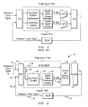
- FIG. 1A is a high level diagram of a conventional PLL incorporating a charge pump an analog loop filter and a trans-conductance (G m ) amplifier as more fully illustrated in FIG. 1B .
- a phase-frequency detector (PFD) receives a reference clock input signal of desired frequency and a feedback signal from a VCO.
- the PFD may be one of numerous designs, including types based on exclusive OR gates or flip flops, which output a pulse signal proportional to positive or negative phase and frequency differences between the clock signal and the feedback signal.
- the VCO may be a three stage ring oscillator circuit having three inverters I 1 , I 2 , I 3 coupled in series as shown in FIG. 1C . Assuming a predetermined bias voltage, the circuit oscillates at a frequency, f, having an associated period 1/f. For this three stage ring, the group delay (or the phase shift) of all 3 stages is 360 degrees. Hence, this means each stage I 1 , I 2 , I 3 has a delay of 120 degrees and, due to the phase shift, the nodes labeled N 1 , N 2 , N 3 will be at different potentials at any instant in time. For example, when one of the nodes is close to V DD , another node will be close to ground (V SS ) and the other node will be at a potential between V DD and ground.
- V SS ground
- the desired VCO frequency, f is a multiple, N, of the reference clock signal frequency, and is factored by the block DIV/N accordingly to provide the suitable feedback signal for comparison to be made by the PFD.
- a phase difference output signal which may comprise a pulse width having a time duration in proportion to the phase difference.
- a charge pump receives the phase difference output signal and generates current in proportion to the phase difference.
- the current output by the charge pump is fed through an analog loop filter to the VCO.
- the design of the loop filter affects response time, bandwidth and stability.
- the combination of the charge pump and the loop filter provides two components of signal to the VCO: a pulse component in proportion to the phase difference, and an integral component which affects the frequency adjustment.
- analog PLL low jitter.
- tuning of the loop filter component for a desired response time and stability in an analog PLL can still result in added noise.
- analog PLL circuits Another limitation of analog PLL circuits is that the analog charge pumps and loop filters have wide range voltage tuning requirements. These are becoming increasingly difficult to meet as manufacturing technologies have moved past the 45 nanometer node to 28 nm technologies and toward, for example, 10 nm linewidths.
- analog PLLs in deep nanometer technologies there are also concerns about relatively high capacitor leakage rates and, generally, disadvantages due to an inability to scale the sizes of analog components with the smaller digital components.
- FIG. 2 illustrates an example of an all digital PLL.
- analog circuit blocks are replaced by converting signals received from the PFD into digital signals, using quantizers or analog-to-digital converters.
- the digital implementation performs digital conversions of the output signals generated by the PFD. Elimination of the capacitor permits better scaling to small fabrication geometries and reduces sensitivity to process variations.
- the illustrated digital PLL has a proportional path, for adjusting the phase of the VCO, which is distinct from a frequency adjusting integral path. The proportional and integral paths undergo separate digital-to-analog conversions for input to the VCO because they each may require conversion of a different number of bits.
- an electronic system includes first subcircuitry and second subcircuitry.
- the first subcircuitry is positioned to provide to the second subcircuitry a supply voltage which is a filtered version of power available from an external power source.
- the first subcircuitry includes a first field effect transistor and a first low pass filter.
- the first field effect transistor has first and second source/drain regions and a gate region.
- the first low pass filter is coupled to receive a signal from the external power source during operation of the second subcircuitry.
- the first filter is also coupled to provide a filtered version of the power source signal to the gate of the first transistor, so that when the first source/drain region of the first transistor is connected to receive power from the external source, and the gate of the first transistor receives the filtered version of the power source signal, the second source/drain region of the first transistor provides a first modified version of the power received from the power source.
- phase locked loop circuitry includes fast integral path circuitry, slow integral circuit path circuitry and proportional path circuitry.
- system comprises serialization or deserialization circuitry with second subcircuitry including a phase locked loop circuit as a component of the serialization or deserialization circuitry.
- FIG. 1A illustrates an analog phase locked loop circuit incorporating a charge pump, an analog loop filter and a trans-conductance (G m ) amplifier;
- FIG. 1B further illustrates components of the circuit shown in FIG. 1A ;
- FIG. 1C illustrates a conventional ring oscillator circuit
- FIG. 2 illustrates a digital phase locked loop circuit
- FIG. 3 illustrates a phase locked loop circuit according to an embodiment of the invention
- FIG. 4 illustrates exemplary quantizer circuitry for the embodiment shown in FIG. 3 ;
- FIG. 5 illustrates exemplary processing circuitry, including an accumulator and a sigma delta modulator, for the embodiment shown in FIG. 3 ;
- FIG. 6A illustrates exemplary control and interface circuitry for the embodiment shown in FIG. 3 , including three paths of control, each providing an adjustment signal;
- FIG. 6B illustrates placement of power supply rejection circuitry in relation to the control and interface circuitry of FIG. 6A ;
- FIGS. 7A-7C illustrate exemplary timing diagrams for an illustrative single ended implementation of proportional path circuitry shown in FIG. 6 to control the timing of operation of the switches;
- FIG. 8 illustrates an exemplary differential implementation of proportional path circuitry which may be applied in lieu of the single ended implementation of proportional path circuitry shown in FIG. 6 ;
- FIGS. 9A-9C are timing diagrams illustrating operation of control signals and current flow in the differential implementation of the proportional path circuitry shown in FIG. 8 ;
- FIG. 10 illustrates an embodiment of a replica circuit 65 having impedance characteristics which suitably match the characteristics of a VCO
- FIG. 11 provides a graphic comparison between voltage-current characteristics of the replica circuit of FIG. 10 and voltage-current characteristics of a VCO;
- FIGS. 12-14 illustrate example embodiments of the power supply rejection circuitry of FIG. 6B ;
- FIG. 15 is a simplified schematic illustration of serializer/deserializer components incorporating phase locked loop circuits according to the invention.
- FIG. 3 illustrates a phase locked loop (PLL) circuit 10 according to an embodiment of the invention.
- a voltage controlled oscillator (VCO) 12 outputs a signal 14 at a terminal 15 thereof, the phase and frequency of which are adjustable based on a comparison between the signal 14 and a clock reference signal 16 .
- the VCO 12 may be the ring oscillator circuit shown in FIG. 1C .
- the desired frequency of the signal 14 is a multiple N of the reference clock signal frequency.
- DIV/N divide by N circuitry
- PFD Phase-Frequency Detector
- the reference clock signal 16 is provided as an input to a terminal 21 of the PFD 20 .
- Control and interface circuitry 22 positioned between the VCO 12 and the PFD 20 , receives inputs both directly and indirectly from the output signal 24 of the PFD 20 , which is in analog form, to provide the VCO 12 with a combination of input signals.
- the input signals to the control and interface circuitry 22 are a combination of the analog version (i.e., the output signal 24 ) and a digitized version of the output signal 24 . Based on the combination of The control and interface
- Operation of the circuitry 22 is controlled with both an analog version and a digital version of the PFD output signal 24 to provide multiple input adjustment signals 30 to the VCO 12 .
- the circuitry 22 receives the output signal 24 in analog form directly from the PFD 20 .
- This analog signal controls switches in proportional path circuitry to provide first adjustment signals (e.g., current signals) to the VCO 12 that contribute to adjustment of the phase of the VCO output signal.
- the circuitry 22 also receives a digitized version of the first analog VCO input signals indirectly from the PFD 20 . This digital signal generates a level of current injection in the circuitry 22 that controls other current signals sent to the VCO, i.e., through integral path circuitry in addition to the proportional path circuitry.
- the digital signal generates a signal (isum) which controls current sent to the VCO 12 through fast integral path circuitry and through slow integral path circuitry.
- the fast integral path circuitry provides a second adjustment signal through a fast integral path to the first input terminal of the VCO.
- the slow integral path circuitry provides a third adjustment signal through a fast integral path to the first input terminal of the VCO.
- the digital signal also provides a level of control to the current signals sent to the VCO 12 through the proportional path circuitry.
- these individual signals referenced in FIG. 3 as a combined signal 30 , adjust the phase and frequency of the VCO 12 relative to the reference signal 16 .
- the PFD 20 generates analog signals UP, DN, UN, DP referred to herein as the signals 24 , which are indicative of a phase-frequency difference between the VCO feedback signal 18 and the clock reference signal 16 .
- the signal UP indicates that an increase in voltage input to the VCO will reduce a phase-frequency difference between the reference clock signal frequency and the feedback signal 18 .
- the signal DN indicates that a decrease in voltage input to the VCO will reduce a phase-frequency difference between the reference clock signal frequency and the feedback signal 18 .
- the signal UN is the inverse of the signal UP and the signal DP is the inverse of the signal DN.
- the signals 24 are provided as a first input, fed directly from the PFD 20 , to the control and interface circuitry 22 .
- the PFD provides a signal 24 every reference clock period
- its output signals, UP and DP are discretized.
- These signals 24 from the PFD 20 are also fed to quantizer circuitry 34 , such as illustrated in FIG. 4 comprising logic circuitry which quantizes the signals 24 , thereby providing as an output a series of digital adjustment signals 36 comprising UPINTN, UPINTP, DNINTP and DNINTN.
- UPINTP is the complement of UPINTN
- DNINTN is the complement of DNINTP.
- the adjustment signals 36 are further processed via digital signal processing circuitry 40 to provide an M bit wide second input signal 38 to the control and interface circuitry 22 .
- the processing circuitry 40 comprises an accumulator 42 and a sigma delta modulator 44 .
- the accumulator 42 is programmable based on algorithm inputs as shown in FIG. 5 .
- the quantizer circuitry 34 and the accumulator 42 operate under the control of a clock signal CLKACC which, in this example, is the same as the reference signal 16 , but the clock signal input to the accumulator 42 may be at a different frequency than the reference clock signal.
- the accumulator receives a series of high resolution, e.g., 22-bit wide, adjustment signals 36 , UPINTP and DNINTP, at, for example, a rate of 100 MHz.
- the modulator 24 operates under a clock signal CLKMOD which may, for example, be three times the frequency of the signal CLKACC.
- the accumulator 42 accumulates 22 bit values based on a difference between the adjustment signals 36 , e.g., (UPINTP ⁇ DNINTP), received from the quantizer 34 , with a programmable gain, and up to 22-bit resolution.
- the variable GAIN controls the speed at which the accumulator accumulates.
- a high GAIN value allows the accumulator 42 to accumulate faster. However, a high GAIN value also introduces more jitter due to increased integral loop gain which degrades stability.
- a low GAIN value allows the accumulator to accumulate at a slower rate.
- a lower GAIN value also decreases the integral loop gain, rendering the PLL more stable. Taking advantage of these conditions, different modes of operation are defined and the optimum GAIN value can be chosen for at least three modes: start up condition, normal operating mode, and special conditions for dynamic modes of operation.
- the frequency of the VCO 12 is adjusted in open loop mode to a frequency very close to the desired frequency.
- the term open loop mode as used herein refers to a state in which the PLL circuit 10 is not in a closed loop mode.
- the difference between the adjusted value in the open loop mode and the desired frequency is 0.5% to 1% of the desired frequency.
- the accumulator is a 22-bit word, accumulating one bit at a time per clock cycle is a very slow process as confirmed by the above equation for ACC[n].
- an algorithm is provided that modulates the GAIN in a logarithmic fashion for each time period.
- the GAIN starts at a very high value, for example, 2 12 .
- the GAIN becomes the previous GAIN value divided by 2. This time delay is programmed from a preset 4-bit register, having a range of 1 to 16 microseconds.
- GAIN GAIN/2.
- the register GAIN is maintained at a fixed value, e.g., 2 3 .
- Special Conditions for Dynamic Modes of Operation occur whenever an external condition disturbs the loop, causing a frequency shift in the VCO output signal 14 .
- the PLL must react quickly to recover from such disturbances and return to frequency and phase locked.
- the integral loop has a relatively slow response time and may require a relatively long period of time in order for the PLL circuit 10 to recover from disturbances.
- the value of the GAIN is changed based on pre-established criteria.
- the criteria may establish a threshold number of cycles during which there are only consecutive signals UPINTP or only consecutive signals DNINTP upon which occurrence the GAIN is changed in accord with a program.
- the GAIN changes dynamically. For example, with a normal mode of operation occurring over a given time period, the GAIN might be 2 3 .
- a threshold algorithm determines that a counter, which only counts consecutive occurrences of the same signal, has reached a threshold number (e.g., eight, corresponding to an occurrence of eight consecutive signals UPINTP, or eight consecutive signals DNINTP), then a dynamic change in the GAIN is triggered.
- a threshold number e.g., eight, corresponding to an occurrence of eight consecutive signals UPINTP, or eight consecutive signals DNINTP
- the same signal e.g., UPINTP
- DNINTP a different signal
- the signal 38 is applied to adjust the VCO input signal 30 .
- the second input signal 38 modifies the frequency of the VCO output signal 14 relative to the reference signal 16 while the first input signal, i.e., the portion of the signal 24 fed directly to the control and interface circuitry 22 , modifies the phase of the VCO output signal 14 .
- the circuitry 22 includes current source signal driving circuitry, also referred to herein as control circuitry 47 , which provides a control signal isum to each of three paths leading to an input node 45 of the VCO 12 .
- the signal isum is delivered to circuitry 46 which forms the fast integral circuit path.
- the signal isum then passes through a low pass filter 49 to provide a signal V bias .
- the signal V bias controls current passing through circuitry 48 which forms the slow integral circuit path.
- the signal V bias is also fed to the circuitry 60 , 60 ′ of the proportional circuit path. See, also, FIG. 8 .
- the control circuitry 47 is connected between a supply voltage rail V DD and a reference or ground rail V SS .
- a diode is formed with a FET 50 having its drain 52 tied to the gate 54 .
- a low pass filter capacitor 58 is connected between the gate 54 and the source 56 of transistor 50 .
- Two digital-to-analog converters (DACs) 62 , 64 are connected in parallel between the drain 52 and V SS .
- the current level from the DAC 62 is set during an initial calibration of the VCO output signal 14 .
- FIG. 8 illustrates an exemplary differential implementation of the proportional path circuitry, indicated as circuitry 60 ′.
- the circuitry 60 , 60 ′ eliminates the need for including a charge pump and an analog loop filter in the proportional path.
- the proportional path circuitry 60 receives the pulse signals UP and DP having variable time widths from the PFD 20 .
- the difference in pulse width between UP and DP is proportional to the phase difference between the clock reference signal 16 and the feedback signal 18 .
- the proportional path circuitry 60 connected between V DD and V SS , is controlled to provide only a proportional path through the input node 45 to the VCO 12 , or only a path through a replica circuit 65 having impedance characteristics which closely follow those of the VCO 12 , or no current flow through either the VCO 12 or the replica circuit 65 .
- the replica circuit 65 is positioned between the node V REP and V SS .
- Switch 66 or 67 In each branch. Operation of the switch 67 is controlled by the signal UP. When the signal UP goes from a low level to a high level the switch 67 is closed. Otherwise the switch 67 is open. Similarly, operation of the switch 66 is controlled by the signal DN. When the signal DN goes from a low level to a high level the switch 66 is closed. Otherwise the switch 66 is open.
- a current minor is set up in the proportional path with a FET 68 .
- the relative delay between the signals UP and DP and the difference in pulse width between the signals UP and DP control the timing of operation of the switches 66 or 67 .
- the signal UP transitions from a logic low level to a logic high level in accord with transitions of the reference clock signal 16 from a low voltage level to a high voltage level, e.g., at fifty percent of the high voltage level.
- the signal DP transitions from a logic low level to a logic high level in accord with transitions of the feedback clock signal 18 from a low voltage level to a high voltage level, e.g., at fifty percent of the high voltage level.
- the switch 67 transitions from an open position to a closed position when the signal UP transitions from a logic low voltage level to a logic high voltage level; and the switch 66 transitions from an open position to a closed position when the signal DP transitions from a logic low voltage level to a logic high voltage level.
- the signal UP transitions from a logic low voltage level to a logic high voltage level a time ⁇ t 1 before the signal DP transitions from a logic low voltage level to a logic high voltage level.
- both the signal UP and the signal DP then transition from a logic high voltage level to a logic low voltage level thereby placing each of the switches 66 , 67 in an open position, terminating current flow through the proportional path circuitry 60 .
- the signal DP transitions from a logic low voltage level to a logic high voltage level a time ⁇ t 2 before the signal UP transitions from a logic low voltage level to a logic high voltage level.
- both the signal UP and the signal DP then transition from a logic high voltage level to a logic low voltage level thereby placing each of the switches 66 , 67 in an open position, terminating current flow through the proportional path circuitry 60 .
- the signals UP and DP when there is no phase difference between the reference clock signal and the feedback clock signal 18 , the signals UP and DP simultaneously transition from a logic low voltage level to a logic high voltage level, whereby both of the switches 66 , 67 are held in an open position, preventing any current flow through the proportional path circuitry 60 .
- the signals UP and DP then simultaneously transition from a logic high voltage level to a logic low voltage level with the switches 66 , 67 still remaining in open configurations such that no current flows through the proportional path circuitry 60 .
- the circuitry 60 ′ includes first and second PMOS FETs 80 , 82 , each acting as a current mirror in one of two cross coupled branches 84 , 86 connected between V DD and V SS , in a manner analogous to the circuitry 60 .
- the source of FET 80 is connected to V DD and the drain of FET 80 is connected to the source of each of two PMOS FETS 90 , 92 .
- the drain of FET 90 is connected as an input to the replica circuit 65 and the drain of FET 92 is connected as an input to the VCO 12 .
- the source of FET 82 is connected to V DD and the drain of FET 82 is connected to the source of each of two PMOS FETS 96 , 98 .
- the drain of FET 96 is connected as an input to the VCO 12 and the drain of FET 92 is connected as an input to the replica circuit 65 .
- the gate of FET 90 receives the control signal UP as described with respect to the circuitry 60
- the gate of FET 98 receives the control signal DN, also as described with respect to the circuitry 60
- the gate of FET 92 receives a control signal UN, which is the complement of the control signal UP
- the gate of FET 96 receives the control signal DP, which is the complement of the control signal DN.
- FIG. 9 are timing diagrams illustrating operation of the control signals in the differential implementation of the proportional circuit path based on the circuitry 60 ′ and the resulting current flow through the proportional circuit path into the VCO 12 . Since the control signals UN and DN are complements of UP and DP, respectively, only UP and DP are expressly shown in FIG. 9 .
- FIG. 9A illustrates logic levels of the control signals and resulting current flow to the VCO 12 when, as described with reference to FIG. 7A , the phase of the reference clock signal 16 leads the phase of the feedback clock signal 18 .
- the phase detector 20 transitions the control signal UP from a logic low voltage level to a logic high voltage level. This places FET 90 in a non-conducting mode, preventing current flow from FET 80 into the replica circuit 65 .
- the signal UP transitions to the logic high voltage level
- the signal UN transitions from a logic high voltage level to a logic low voltage level.
- FET 92 in a conducting mode, sending current from FET 80 into the VCO 12 during the time interval ⁇ t 1 .
- the control signal DP Prior to and during the time interval ⁇ t 1 (i.e., before the feedback clock signal 18 , shown in FIG. 7A , transitions from a low voltage level to a high voltage level) the control signal DP is at a logic low voltage level and the complement DN is at a logic high voltage level.
- FET 96 prior to and during the time that FET 92 is in a conducting state, FET 96 is also in a conducting state, sending current from FET 82 into the VCO 12 .
- FET 98 is in a non-conducting mode, preventing current flow from FET 82 into the replica circuit 65 . Consequently, during the time interval ⁇ t 1 , both of the branches 84 and 86 feed current to the VCO 12 while the replica circuit 65 receives no current. Thus the current into the VCO increases from a steady state level to a higher level during the period ⁇ t 1 .
- the feedback clock signal 18 transitions from a low voltage level to a high voltage level, such that the phase detector 20 transitions the control signal DP from a logic low voltage level to a logic high voltage level, after which time the phase detector transitions both the signal UP and the signal DP from logic high voltage levels to logic low voltage levels.
- complements of each, UN and DN transition from logic low voltage levels to logic high voltage levels.
- FIG. 9B illustrates logic levels of the control signals and resulting current flow to the VCO 12 when, as described with reference to FIG. 7B , the phase of the reference clock signal 16 lags the phase of the feedback clock signal 18 .
- the phase detector 20 transitions the control signal DP from a logic low voltage level to a logic high voltage level. This places FET 96 in a non-conducting mode, preventing current flow from FET 82 into the VCO 12 .
- the signal DN transitions from a logic high voltage level to a logic low voltage level.
- FET 98 is in a conducting mode, sending current from FET 82 into the replica circuit 12 during the time interval ⁇ t 2 .
- the control signal UP is at a logic low voltage level and the complement UN is at a logic high voltage level.
- FET 90 is also in a conducting state, sending current from FET 80 into the replica circuit 65 .
- FET 92 is in a non-conducting mode, preventing current flow from FET 80 , through FET 92 and into the VCO 12 .
- both of the branches 84 and 86 feed current to the replica circuit 65 while the VCO 12 receives no current from either of the branches 84 , 86 .
- the current into the VCO decreases from a steady state level to a lower level during the period ⁇ t 2 .
- the reference clock signal 16 transitions from a low voltage level to a high voltage level, such that the phase detector 20 transitions the control signal UP from a logic low voltage level to a logic high voltage level, after which time the phase detector transitions both the signal UP and the signal DP from logic high voltage levels to logic low voltage levels.
- FIG. 9C illustrates logic levels of the control signals and resulting current flow to the VCO 12 when, as described with reference to FIG. 7C , there is no phase difference between the reference clock signal 16 and the feedback clock signal 18 .
- the phase detector 20 transitions both of the control signals UP and DP from a logic low voltage level to a logic high voltage level. This places FETs 90 and 96 in a non-conducting mode, preventing current flow from FET 80 into the replica circuit 65 and preventing current flow from FET 82 into the VCO 12 .
- the control signals UN and DN both transition from a logic high voltage level to a logic low voltage level.
- FET 92 feeds current to the VCO
- FET 98 feeds current to the replica circuit
- FET 96 feeds current to the VCO
- FET 90 feeds current to the replica circuit.
- phase detector then transitions the control signals back to the values corresponding to the steady state condition where UP and DP are at logic low voltage levels and UN and DN are at logic high voltage levels such that the VCO again receives the steady state current level through FET 96 only and the replica circuit receives a similar current level through FET 90 only.
- Operation of the proportional path circuitry 60 ′ according to the illustrated examples of FIG. 9 is characterized by relatively smooth transitions as different FETs simultaneously switch in and out of conduction.
- all of the transistors 90 , 92 , 96 and 98 have identical characteristics. More generally, in other embodiments, the FETs 92 , 96 and the FETs 90 , 98 are matched pairs.
- the replica circuit 65 In the illustrated proportional path circuitry, stabilization of the voltage input to the replica circuit 65 , with respect to the voltage input to the VCO 12 , is not based on feedback. Instead, to minimize injection of transient glitches into the VCO during operation of the proportional path circuitry, the replica circuit 65 closely matches the voltage—impedance characteristics of the VCO 12 .
- An embodiment of a replica circuit 65 having impedance characteristics which suitably match the characteristics of the VCO 12 is shown in FIG. 10 . Recognizing that the VCO 12 is a non-linear device, the replica circuit 65 is a DC circuit which emulates the input impedance characteristics of the VCO. That is, when the input into the VCO 12 changes, the impedance of the VCO also changes.
- FIG. 11 illustrates how the voltage-current characteristics V REP of the replica circuit 65 track the voltage-current characteristics V OSC of the VCO 12 .
- the phase locked loop (PLL) circuit 10 not incorporating charge pump circuitry to store charge in a capacitor for input to the voltage controlled oscillator, the impedance characteristics of the replica circuit 65 and the VCO 12 are so matched that current-voltage characteristics of these two impedance devices can be within five percent of one another throughout the voltage operating range of the VCO.
- the system does not incorporate charge pump circuitry to store charge in a capacitor for input to the voltage controlled oscillator.
- the impedance characteristics of the replica circuit 65 can so closely follow the impedance characteristics of the voltage controlled oscillator as a function of voltage level as to allow a voltage level to be switched between the subcircuit 65 and the voltage controlled oscillator 12 without creating voltage spikes, when a voltage level is switched between the replica circuit 65 and the VCO. More generally, when a voltage level is switched between the replica circuit and the VCO 12 , voltage spikes can be controlled to a range between zero and two percent of the operating voltage applied to the VCO.
- the replica circuit 65 is a static DC circuit which tracks the impedance characteristics of a dynamic circuit such as the three stage inverter ring oscillator of FIG. 1C .
- the group delay, i.e., the collective phase shift, of the three stages is 360°.
- each inverter stage has a delay of 120° and each of the nodes I 1 , I 2 , and I 3 , due to the phase shift, will be at a different potential (gate to ground) at any given time.
- the device 102 is a PMOS FET having the gate connected to ground. This corresponds to one or more of the PMOS transistors in FIG.
- the device 108 is an NMOS FET having the gate connected to V REP . This represents one or more of the NMOS transistors in FIG. 1C when the potential of one of the nodes I 1 /I 2 /I 3 is close to V OSC .
- the gate of the PMOS FET 104 is connected to a node between the FETs 106 and 108 , resulting in a gate potential which is neither low nor high such that the NMOS FET 104 , connected to a node between 102 and 104 that is neither at V REP or ground.
- the devices 102 and 108 operate in triode mode, which corresponds to the impedances of some of the transistors in the VCO ring that are fully switched due to their gate biasing voltage being at V REP or ground; while the devices 104 and 106 operate in the saturation mode which corresponds to the impedances of some of the transistors in the VCO ring oscillator that are partially switched on due to their gates being biased at a voltage between V REP and ground.
- the proportional path circuitry 60 , 60 ′ receives inputs from the PFD 20 which generates pulses where the pulse width difference is proportional to the phase difference of the feedback clock and the reference clock.
- the proportional path has three modes of operation based on the signals UP, UN, DP, and DN.
- FIG. 9A the phase of the reference clock is shown to lead the feedback clock and there is a positive current injection into the VCO.
- FIG. 9B the phase of the reference clock is shown to lag the feedback clock. Hence there is negative current injection into the VCO.
- FIG. 9C illustrates the condition where there is no phase mismatch between the reference clock and the feedback clock. Hence, there is no change in the total net current injected into the VCO.
- the charge pump, loop filter, and trans-conductance amplifier have been necessary to translate the full swing up and down signals from the PFD into the VCO as described with respect to FIG. 1B .
- Use of a loop filter having a large passive device is a growing impediment in monolithic manufacturing processes that move past the 45 nanometer node.
- the loop filter provides a path for noise transfer to the VCO.
- the proportional path is simplified in accord with FIGS. 3 , 6 and 8 , resulting in several advantages.
- the small signal G m amplifier is a wide band device because it typically needs to process signals with a bandwidth up to several hundred megahertz.
- V REP closely follows V OSC , allowing large currents to be switched between the replica circuit 65 and the VCO 12 without creating large current spikes.
- the circuitry 46 which forms the fast integral path comprises a FET 122 connected between V DD and the input node 45 .
- the source terminal of the FET 122 is connected to V DD and the drain terminal of the FET 122 is connected to the node 45 .
- the fast integral path circuitry 46 is programmable and in the present embodiment conducts up to twenty percent of the total input current to the VCO 12 , e.g., ten percent.
- the cut-off frequency of signals propagating through the fast integral path circuitry 46 is limited by the transconductance of the FET 50 and the capacitor 58 .
- the capacitance is selectable to limit the amount of noise passing into the FET 122 .
- the bandwidth of the Device 122 is about ten MHz.
- the circuitry 48 which forms the slow integral path comprises a FET 126 connected between V DD and the input node 45 .
- the source terminal of the FET 126 is connected to V DD and the drain terminal of the FET 126 is connected to the node 45 .
- the circuitry 48 includes the low pass filter 49 through which the signal isum passes to remove high frequency noise before input to the gate 130 of the FET 126 .
- the bandwidth of the low pass filter 49 is programmable, i.e., adjustable, and may, for example, range from five KHz to one MHz, thus limiting the bandwidth of devices 126 and 68 to the same range.
- signal propagation through the proportional path circuitry is controlled by switches 66 , 67 (see FIG. 6A ), where device 68 provides the bias current.
- the proportional path bandwidth is limited by the impedance at the input node 45 , which varies between 100 MHz and 400 MHz.
- the fast integral path (circuitry 46 ) and the slow integral circuit path (circuitry 48 ) control the frequency of the VCO 12 .
- Changes in application environmental parameters e.g., temperature and supply voltage, can affect the frequency of the VCO output signal 14 .
- a change in the absolute temperature changes transistor switching speeds which result in a change in VCO frequency.
- the integral path compensates for the VCO frequency variations due to these parameters and stabilizes the VCO frequency at the desired value.
- Parameters such as off chip supply voltage and temperature change at a very slow rate, typically at kilo-hertz rate or slower.
- the slow integral path is designed to operate at a bandwidth as low as five KHz.
- other parameters such as reference clock frequency modulation can be set as high as 133 KHz.
- the fast integral loop is designed to operate at a ten MHz bandwidth to ensure it can remove frequency errors due to reference clock frequency modulation. In both cases, the bandwidth should be higher than the possible change rate in order to quickly correct for deviations resulting from these
- the phase locked loop circuit 10 comprises Power Supply Rejection (PSR) subcircuitry 132 connected to provide the supply voltage V DD to other subcircuitry 133 of the phase locked loop circuit 10 , including the control and interface circuitry 22 (e.g., fast integral path circuitry 46 , control circuitry 47 , slow integral circuit path circuitry 48 and proportional path circuitry 60 , 60 ′).
- PSR Power Supply Rejection
- Example designs of the PSR subcircuitry 132 shown in FIGS. 12-14 are referenced as subcircuitry 132 a , 132 b and 132 c.
- the disclosed embodiments incorporate field effect transistors (FETs) but the invention is not so limited.
- FETs field effect transistors
- the term region refers to a distinct and identifiable portion of a transistor, such as a source, a drain or a gate, and the term region may be used interchangeably with any one of these and interchangeably with a terminal to which one of these is in electrical conduction.
- the term source/drain region as used herein means a semiconductor region or a terminal leading to the semiconductor region wherein the region operates as a source or as a drain of a transistor device.
- Filter or filter element means one or more capacitor devices, which are illustrated herein as two terminal devices.
- a filter element may include one or more resistors, and reference to a filter element includes reference to impedance networks generally.
- the term filter refers to a filter which may be an analog filter or a digital filter.
- Low pass filter means a filter which is has a frequency characteristic wherein above a given frequency there is notable signal attenuation.
- Terminal and connection may refer to a point of contact which effects connection although in highly integrated circuitry a physical connection may not be a characterized by a distinct connection point which can be isolated from other conductive material.
- reference to a point of connection or a terminal which receives a source of external power or voltage is to be understood as a point in circuitry which may receive such power or voltage during circuit operation but which may not be present when the circuitry is not operating.
- the circuitry of FIG. 12 is exemplary of filter circuitry providing power supply rejection for the exemplary phase locked loop subcircuitry 133 .
- PSR subcircuitry 132 a is connected to an exemplary terminal or connection point 139 to receive a first supply voltage P v from a source external to the phase locked loop circuit 10 and provide a second supply voltage, V DD , to the phase locked loop subcircuitry 133 through an exemplary connection 137 b .
- the PSR subcircuitry 132 a is configured with the drain 136 d of a NMOS transistor 136 connected to an exemplary terminal 137 a at which the supply voltage P v may be provided from the external source.
- the source 136 s of the NMOS transistor 136 is connected to provide current to the phase locked loop subcircuitry 133 through an exemplary connection 137 b .
- a low pass filter 138 is connected between the gate 136 g of the transistor 136 and the exemplary terminal or connection point 139 to drive the high impedance gate 136 g of the transistor with a filtered version of the signal derived from the first supply voltage P v when received from the external supply voltage source.
- Application of the filtered version of the signal to the gate 136 g provides a voltage V DD at the source terminal 137 b which exhibits power supply rejection above a cut-off frequency set by the filter, i.e., determined in part by the filter characteristics. Below the cut-off frequency V DD tracks P v .
- V DD does not track variations in the supply voltage P v .
- additional NMOS transistors and or filters may be stacked to increase the amount of power supply rejection. See, for example, the circuits of FIGS. 12 and 13 .
- the circuitry of FIG. 13 includes PSR subcircuitry 132 b connected to receive a first supply voltage P v and provide a second supply voltage V DD to the phase locked loop subcircuitry 133 through the exemplary connection 137 b .
- the PSR subcircuitry 132 b comprises a resistor-capacitor network and multiple PMOS transistors.
- two transistors 150 , 152 , two low pass filters 154 , 156 and two resistors 158 , 160 are illustrated, it being understood that other embodiments may comprise additional transistors, low pass filters and resistors.
- the transistors 150 , 152 are arranged in series with the source 150 s of the transistor 150 connected to an exemplary power supply terminal 137 a at which a supply voltage P v may be provided from a source external to the PLL circuit 10 .
- the drain 150 d of the PMOS transistor 150 is connected to the source 152 s of the PMOS transistor 152 .
- the drain 152 d of the PMOS transistor 152 is connected to provide current to the phase locked loop subcircuitry 133 through the exemplary connection 137 b.
- the high impedance gates 150 g 152 g of the two PMOS transistors 150 , 152 are each connected to an exemplary terminal or connection point 139 , at which the supply voltage P v may be received from a source external to the PLL circuit 10 .
- Resistors 158 and 160 are positioned between P v and a reference terminal V SS .
- Each of the two low pass filters 154 , 156 is connected on a different side of the resistor 158 while the resistor 160 further limits current flow to V SS .
- the gate 150 g of the transistor 150 is connected through the low pass filter 154 is driven with a signal derived from the first supply voltage P v when received from the external supply voltage source.
- the gate 152 g of the transistor 152 is connected in series through the low pass filter 156 and the resistor 160 to also receive and be driven with a signal derived from the first supply voltage P v , when received from the external supply voltage source.
- the filter 156 is connected between the gate 152 g and a connection point 161 a between the resistor 158 and the resistor 160 . With this arrangement the drain 150 d of the first transistor 150 provides a first modified limits current flow to V SS .
- the filters 154 , 156 provide the supply voltage V DD at the terminal 137 b which exhibits power supply rejection above a cut-off frequency set by the filters 154 , 156 , i.e., determined in part by the filter characteristics. Below the cut-off frequency V DD tracks P v . Above the cut-off frequency V DD does not track variations in the supply voltage P v . In other embodiments, additional transistors and filters may be incorporated in the subcircuitry 132 b to increase the amount of power supply rejection.
- the circuitry of FIG. 14 includes PSR subcircuitry 132 c connected to receive a first supply voltage P v and provide a second supply voltage V DD to the phase locked loop subcircuitry 133 through the exemplary connection 137 b .
- the PSR subcircuitry 132 c comprises a resistor-capacitor network and multiple PMOS transistors.
- two PMOS transistors 150 , 152 , two low pass filters 154 , 156 and two resistors 158 , 160 are illustrated, it being understood that other embodiments may comprise additional transistors, low pass filters and resistors.
- the transistors 150 , 152 are arranged in series with the source 150 s of the transistor 150 connected to an exemplary power supply terminal 137 a at which a supply voltage P v may be provided from a source external to the PLL circuit 10 .
- the drain 150 d of the PMOS transistor 150 is connected to the source 152 s of the PMOS transistor 152 .
- the drain 152 d of the PMOS transistor 152 is connected to provide current to the phase locked loop subcircuitry 133 through the exemplary connection 137 b .
- the high impedance gates 150 g 152 g of the two PMOS transistors 150 , 152 are each connected to one or more exemplary terminal or connection points 139 , at which the supply voltage P v may be received from a source external to the PLL circuit 10 .
- Resistors 158 and 160 are positioned between P v and a reference terminal V SS .
- the low pass filter 154 is connected at a node 161 between the resistors 158 , 160 so that the gate 150 g of the transistor 150 is connected in series, through the filter 154 and the resistor 158 , to be driven with a signal derived from the first supply voltage P v , when received from the external supply voltage source at a terminal or connection point 139 .
- the resistor 160 further limits current flow to V SS .
- the low pass filter 156 is connected between the gate 152 g of the transistor 152 and a terminal or connection point 139 to receive a signal derived from the first supply voltage P v when received from the external supply voltage source, and drive the gate 152 g of the transistor 152 with the derived signal.
- the low pass filter 154 is connected at a node 161 b between the resistors 158 , 160 so that the gate 150 g of the transistor 150 is connected in series, through the filter 154 and the resistor 158 , to be driven with a signal derived from the first supply voltage P v , when received from the external supply voltage source at a terminal or connection point 139 .
- the resistor 160 further limits current flow to V SS .
- the low pass filter 156 is connected between the gate 152 g of the transistor 152 and a terminal or connection point 139 to receive a signal derived from the first supply voltage P v when received from the external supply voltage source, and drive the gate 152 g of the transistor 152 with the derived signal.
- the transistors are kept in saturation to provide maximum power supply rejection, but they can operate in other regions.
- the regulated supply voltage V DD moves with respect to P v up to the bandwidth of the low pass filter whereas, in previous designs, the supply going to the VCO has been regulated via feedback to ensure the supply stays constant.
- the phase locked loop circuit 10 runs with lower jitter than a typical analog PLL, but contains a reduced number of analog blocks compared to an analog PLL.
- the VCO 12 is an analog component while all other components are digital, this rendering the design more suitable for low voltage operation and more portable to current and future small geometry manufacturing technologies.
- PLL circuits according to the invention are also much less process and environmentally sensitive than PLL analog designs.
- K VCO is the only process sensitive parameter in the loop dynamics of the PLL circuit 10 . This results in relatively stable operation, making the PLL circuit 10 very robust and suitable for large volume production.
- phase locked loop circuitry having a triple path for phase and frequency control, there being a proportional path, a fast integral path and a slow integral path; (2) programmable control of the slow integral path by adjusting its bandwidth for use in loop dynamics; and (3) an open regulation technique which does not use feedback to achieve power supply rejection.
- the proportional path eliminates the need for a charge pump, loop filter, or equivalent digital PLL techniques by its direct usage in switching current up to 40% of the total VCO bias current.
- An embodiment uses a filtered clean bias voltage from the slow integral path to bias the proportional path current.
- a new static no feedback replica circuit is disclosed which tracks a dynamic circuit's average switching current.
- inventive concepts may be advantageously applied in a variety of electronic systems.
- Serdes serializer/deserializer devices
- data is serialized to reduce the level of parallelism. This reduces the pin count of each device, but the data transfer frequency increases in inverse proportion to the ratio by which the pin count is reduced.
- each device establishes a data transfer rate by multiplying a reference clock speed with intermediate frequency PLL circuitry.
- FIG. 15 is a simplified schematic illustrating a serializer 162 from which data is transferred in a first device 164 (e.g., a first integrated circuit) to a deserializer 166 in a second device 168 (e.g., a second integrated circuit).
- the first device 164 is a component of a first system 170 and may be mounted on a first pc board.
- the second device 168 is a component of a second system 171 and may be mounted on a second pc board.
- the serializer 162 receives m-bit wide parallel data from circuitry 167 within the first device 164 and converts the data to a lower bit width, k, of parallel data for transfer along the serialized data line 172 to the deserializer 166 which then performs a post transfer restoration of the data to the original m-bit width for operation thereon by other circuitry in the second device 168 .
- the serializer 162 and the deserializer 166 each include one or more phase locked loop circuits 10 which receive a reference clock signal to facilitate operation of first control circuitry 173 of the serializer 162 or operation of second control circuitry 175 of the deserializer 166 .
- the m-bit wide data is initially received by first input circuitry 174 of the serializer, then undergoes parallel-to-serial conversion in serialization block 176 , from which the data passes through first output circuitry 178 and are then transmitted off chip via the data line 172 .
- the serialized data stream is received by the second input circuitry 184 of the deserializer 166 and then undergoes serial-to-parallel conversion in deserialization block 186 to recreate m-bit wide parallel data which pass through second output circuitry 188 to other circuitry 190 in the second device 168 for processing.
- inventive concepts may be implemented on two separate systems 170 and 171 , each having a device comprising circuitry (i) for performing serialization of data from a m-bit wide parallel arrangement to a k-bit wide parallel arrangement for transfer of the data to another device, or (ii) for performing deserialization of data from a k-bit wide parallel arrangement to a m-bit wide parallel arrangement for transfer of the data to another device, where k ⁇ m.
- DLL delay locked loop
- DLL circuitry to adjust the phase of a signal or for clock recovery.
- phase locked loop circuitry 10 it will be understood by those skilled in the art that such DLL circuitry according to the invention will comprise phase detector circuitry in lieu of the illustrated phase and frequency detector 20 , and a chain of delay gates in lieu of the VCO 12 .
- DLL circuitry incorporating features of the invention may be integrated into, for example, memory devices such as Dynamic Random Access Memory (DRAM) devices.
- DRAM Dynamic Random Access Memory
Abstract
Description
ACC[n]=ACC[n−1]+GAIN*(UPINTP−DNINTP)
for n samples. The variable GAIN controls the speed at which the accumulator accumulates. A high GAIN value allows the
GAIN=GAIN/2.
If (consecutive UPINTP or consecutive DNINTP is met) then GAIN=GAIN*2
GAIN=GAIN/2
thereby reverting to the GAIN value applied during the normal mode of operation, e.g., 23. Also, each time the counter is incremented above the zero value but stops because two or more consecutive values of the same signal (e.g., UPINTP) are followed by a different signal (e.g., DNINTP), the counter is reset.
F cut-off =K VCO/(2πN) (1)
where KVCO is the analog tuning gain of the VCO and N is the PLL feedback divider value (DIV/N). As can be seen from Equation (1), KVCO is the only process sensitive parameter in the loop dynamics of the
Claims (16)
Priority Applications (4)
| Application Number | Priority Date | Filing Date | Title |
|---|---|---|---|
| US13/543,982 US8829982B2 (en) | 2011-07-28 | 2012-07-09 | System incorporating power supply rejection circuitry and related method |
| PCT/US2012/046027 WO2013015977A1 (en) | 2011-07-28 | 2012-07-10 | Circuitry and method for controlling a characteristic of a periodic signal |
| CN201280047265.6A CN103828240B (en) | 2011-07-28 | 2012-07-10 | Circuit and method for the characteristic of controlling cycle signal |
| DE112012003149.0T DE112012003149B4 (en) | 2011-07-28 | 2012-07-10 | System and method for controlling a characteristic of a periodic signal |
Applications Claiming Priority (2)
| Application Number | Priority Date | Filing Date | Title |
|---|---|---|---|
| US201161512549P | 2011-07-28 | 2011-07-28 | |
| US13/543,982 US8829982B2 (en) | 2011-07-28 | 2012-07-09 | System incorporating power supply rejection circuitry and related method |
Publications (2)
| Publication Number | Publication Date |
|---|---|
| US20130027119A1 US20130027119A1 (en) | 2013-01-31 |
| US8829982B2 true US8829982B2 (en) | 2014-09-09 |
Family
ID=47596722
Family Applications (6)
| Application Number | Title | Priority Date | Filing Date |
|---|---|---|---|
| US13/543,971 Active US8513995B2 (en) | 2011-07-28 | 2012-07-09 | System including circuitry providing multiple circuit paths for controlling a characteristic of a period signal |
| US13/543,975 Expired - Fee Related US8581644B2 (en) | 2011-07-28 | 2012-07-09 | System and method providing bandwidth adjustment in integral path of phase locked loop circuitry |
| US13/543,982 Expired - Fee Related US8829982B2 (en) | 2011-07-28 | 2012-07-09 | System incorporating power supply rejection circuitry and related method |
| US13/543,991 Expired - Fee Related US8664986B2 (en) | 2011-07-28 | 2012-07-09 | System, method and emulation circuitry useful for adjusting a characteristic of a periodic signal |
| US13/544,001 Expired - Fee Related US8508270B2 (en) | 2011-07-28 | 2012-07-09 | System and method for adjusting a characteristic of a periodic signal with use of a filtered bias voltage |
| US13/543,961 Active US8432203B2 (en) | 2011-07-28 | 2012-07-09 | System including circuitry for controlling a characteristic of a periodic signal and method for adjusting a signal |
Family Applications Before (2)
| Application Number | Title | Priority Date | Filing Date |
|---|---|---|---|
| US13/543,971 Active US8513995B2 (en) | 2011-07-28 | 2012-07-09 | System including circuitry providing multiple circuit paths for controlling a characteristic of a period signal |
| US13/543,975 Expired - Fee Related US8581644B2 (en) | 2011-07-28 | 2012-07-09 | System and method providing bandwidth adjustment in integral path of phase locked loop circuitry |
Family Applications After (3)
| Application Number | Title | Priority Date | Filing Date |
|---|---|---|---|
| US13/543,991 Expired - Fee Related US8664986B2 (en) | 2011-07-28 | 2012-07-09 | System, method and emulation circuitry useful for adjusting a characteristic of a periodic signal |
| US13/544,001 Expired - Fee Related US8508270B2 (en) | 2011-07-28 | 2012-07-09 | System and method for adjusting a characteristic of a periodic signal with use of a filtered bias voltage |
| US13/543,961 Active US8432203B2 (en) | 2011-07-28 | 2012-07-09 | System including circuitry for controlling a characteristic of a periodic signal and method for adjusting a signal |
Country Status (4)
| Country | Link |
|---|---|
| US (6) | US8513995B2 (en) |
| CN (1) | CN103828240B (en) |
| DE (1) | DE112012003149B4 (en) |
| WO (1) | WO2013015977A1 (en) |
Families Citing this family (37)
| Publication number | Priority date | Publication date | Assignee | Title |
|---|---|---|---|---|
| WO2012001846A1 (en) * | 2010-06-28 | 2012-01-05 | パナソニック株式会社 | Reference frequency generating circuit, semiconductor integrated circuit and electronic apparatus |
| US9157950B2 (en) | 2011-04-18 | 2015-10-13 | International Business Machines Corporation | Loop parameter sensor using repetitive phase errors |
| US8513995B2 (en) * | 2011-07-28 | 2013-08-20 | Intel Corporation | System including circuitry providing multiple circuit paths for controlling a characteristic of a period signal |
| US8493113B2 (en) * | 2011-09-12 | 2013-07-23 | International Business Machines Corporation | PLL bandwidth correction with offset compensation |
| US8718216B2 (en) * | 2011-09-23 | 2014-05-06 | International Business Machines Corporation | Digital phase detector with zero phase offset |
| US8704570B2 (en) * | 2011-12-20 | 2014-04-22 | Mosys, Inc. | Delay-locked loop with phase adjustment |
| US8698567B2 (en) * | 2012-04-02 | 2014-04-15 | Avago Technologies General Ip (Singapore) Pte. Ltd. | Phase-locked loop calibration system and method |
| US9065457B2 (en) * | 2012-04-26 | 2015-06-23 | Skyworks Solutions, Inc. | Circuits and methods for eliminating reference spurs in fractional-N frequency synthesis |
| US8989332B2 (en) * | 2012-04-26 | 2015-03-24 | Skyworks Solutions, Inc. | Systems and methods for controlling frequency synthesis |
| US8704566B2 (en) * | 2012-09-10 | 2014-04-22 | International Business Machines Corporation | Hybrid phase-locked loop architectures |
| US8957711B2 (en) * | 2013-04-29 | 2015-02-17 | Microsemi Semiconductor Ulc | Phase locked loop with precise phase and frequency slope limiter |
| EP3010058B1 (en) * | 2013-07-19 | 2021-02-17 | LG Display Co., Ltd. | Electrode laminate and organic light emitting element |
| US9300277B2 (en) * | 2013-12-17 | 2016-03-29 | Intel Corporation | Apparatus for reducing periodic jitter in a ring oscillator |
| US9209821B2 (en) | 2014-01-24 | 2015-12-08 | Intel Corporation | Apparatus for generating quadrature clock phases from a single-ended odd-stage ring oscillator |
| JP6254014B2 (en) * | 2014-02-27 | 2017-12-27 | パナソニック株式会社 | Harmonic rejection power amplifier |
| US9455727B2 (en) | 2014-09-26 | 2016-09-27 | Intel Corporation | Open-loop voltage regulation and drift compensation for digitally controlled oscillator (DCO) |
| EP3007013A1 (en) * | 2014-10-07 | 2016-04-13 | The Swatch Group Research and Development Ltd. | Position sensor for a timepiece setting stem |
| SI3045212T1 (en) | 2015-01-19 | 2019-10-30 | Flisek Razvoj Proizvodnja In Trgovina Z Izdelki Za Sport D O O | Ski edge and sidewall cross section profile |
| JP6569946B2 (en) * | 2015-04-08 | 2019-09-04 | パナソニックIpマネジメント株式会社 | Storage battery pack, storage battery pack control method, and information terminal control method |
| US9438254B1 (en) * | 2015-05-21 | 2016-09-06 | Stmicroelectronics International N.V. | Charge pump circuit for a phase locked loop |
| JP6585963B2 (en) | 2015-08-24 | 2019-10-02 | ルネサスエレクトロニクス株式会社 | PLL circuit and operation method |
| CN105979626B (en) | 2016-05-23 | 2018-08-24 | 昂宝电子(上海)有限公司 | The two-terminal integrated circuit with time-varying voltage current characteristics including locking phase power supply |
| US9900943B2 (en) | 2016-05-23 | 2018-02-20 | On-Bright Electronics (Shanghai) Co., Ltd. | Two-terminal integrated circuits with time-varying voltage-current characteristics including phased-locked power supplies |
| US20180170242A1 (en) * | 2016-12-19 | 2018-06-21 | Pilot, Inc. | Bluetooth-enabled vehicle lighting control hub |
| CN108282162B (en) * | 2017-01-06 | 2021-08-31 | 联咏科技股份有限公司 | Clock and data recovery circuit with improved jitter tolerance |
| CN111183587A (en) * | 2017-10-12 | 2020-05-19 | 辛纳普蒂克斯公司 | Phase-locked loop sampler and restorer |
| CN107896309B (en) * | 2017-11-08 | 2019-12-24 | 浙江大华技术股份有限公司 | Method, device and computer readable storage medium for adjusting local carrier frequency |
| US10523411B2 (en) * | 2018-03-29 | 2019-12-31 | Intel Corporation | Programmable clock data recovery (CDR) system including multiple phase error control paths |
| US10848138B2 (en) * | 2018-09-21 | 2020-11-24 | Taiwan Semiconductor Manufacturing Co., Ltd. | Method and apparatus for precision phase skew generation |
| US11017184B2 (en) * | 2018-10-26 | 2021-05-25 | Sendyne Corporation | Runtime-calibratable analog computing system and methods of use |
| KR102608980B1 (en) * | 2018-12-17 | 2023-11-30 | 에스케이하이닉스 주식회사 | Temperature sensor |
| CN109656308B (en) * | 2018-12-18 | 2020-10-27 | 龙芯中科技术有限公司 | Frequency configuration adjusting method and device, electronic equipment and storage medium |
| US10715155B1 (en) * | 2019-10-14 | 2020-07-14 | Ciena Corporation | Apparatus and methods for digital phase locked loop with analog proportional control function |
| CN114779870B (en) * | 2022-05-11 | 2023-10-20 | 中科芯磁科技(珠海)有限责任公司 | Voltage self-adaptive adjusting circuit and chip |
| CN115268570B (en) * | 2022-08-05 | 2023-05-26 | 江苏云涌电子科技股份有限公司 | IRIG-B code time setting system |
| CN116505940B (en) * | 2023-06-26 | 2024-02-23 | 深圳市锦锐科技股份有限公司 | Low-noise PLL phase-locked loop circuit |
| CN117526932A (en) * | 2024-01-08 | 2024-02-06 | 芯耀辉科技有限公司 | Clock signal generation method and device |
Citations (32)
| Publication number | Priority date | Publication date | Assignee | Title |
|---|---|---|---|---|
| US5767713A (en) | 1995-12-08 | 1998-06-16 | Cypress Semiconductor, Inc. | Phase locked loop having integration gain reduction |
| US5802123A (en) | 1993-12-24 | 1998-09-01 | Sony Corporation | Clock signal reproduction circuit and data reproduction circuit |
| US5912575A (en) * | 1996-09-24 | 1999-06-15 | Mitsubishi Electric Semiconductor Software Co., Ltd. | Phase-locked loop circuit with charge pump and time constant circuit |
| US5920488A (en) | 1990-10-01 | 1999-07-06 | American Auto-Matrix, Inc. | Method and system for maintaining a desired air flow through a fume hood |
| US5978425A (en) | 1997-05-23 | 1999-11-02 | Hitachi Micro Systems, Inc. | Hybrid phase-locked loop employing analog and digital loop filters |
| US6242956B1 (en) | 1999-10-22 | 2001-06-05 | Motorola, Inc. | Phase locked loop |
| US6441660B1 (en) * | 2001-02-02 | 2002-08-27 | Broadcom Corporation | High speed, wide bandwidth phase locked loop |
| US6509727B2 (en) * | 2000-11-24 | 2003-01-21 | Texas Instruments Incorporated | Linear regulator enhancement technique |
| US20030169099A1 (en) * | 2001-12-28 | 2003-09-11 | Futoshi Fujiwara | High PSRR current source |
| US6690240B2 (en) | 2002-01-10 | 2004-02-10 | Cirrus Logic, Inc. | Low-jitter loop filter for a phase-locked loop system |
| US6998923B2 (en) | 2003-09-18 | 2006-02-14 | Cirrus Logic, Inc. | Low-noise loop filter for a phase-locked loop system |
| US7102403B2 (en) | 2005-02-03 | 2006-09-05 | Mediatek Incorporation | Clock recovering circuit utilizing a delay locked loop for generating an output clock locked to an analog input signal and related method thereof |
| US20060244490A1 (en) | 2005-04-29 | 2006-11-02 | Samsung Electronics Co., Ltd. | Method and circuit for controlling a refresh of a semiconductor memory device |
| US20070018699A1 (en) | 2005-07-20 | 2007-01-25 | M/A-Com, Inc. | Partial cascode phase locked loop architecture |
| US7177611B2 (en) | 2004-07-07 | 2007-02-13 | Texas Instruments Incorporated | Hybrid control of phase locked loops |
| US7203261B2 (en) | 2003-04-07 | 2007-04-10 | Qualcomm Incorporated | Phase locked loop for an OFDM system |
| US20070165708A1 (en) | 2006-01-17 | 2007-07-19 | Hooman Darabi | Wireless transceiver with modulation path delay calibration |
| US20080068056A1 (en) * | 2006-09-14 | 2008-03-20 | Rambus, Inc. | Power supply noise rejection in PLL or DLL circuits |
| US7382201B1 (en) | 2007-03-23 | 2008-06-03 | Mediatek Inc. | Signal generating apparatus and method thereof |
| US7432751B2 (en) | 2004-04-02 | 2008-10-07 | Teradyne, Inc. | High performance signal generation |
| US20090085679A1 (en) | 2007-09-28 | 2009-04-02 | Richard Ellis Jennings | Dual path phase locked loop (pll) with digitally programmable damping |
| US7580497B2 (en) | 2005-06-29 | 2009-08-25 | Altera Corporation | Clock data recovery loop with separate proportional path |
| US7642822B2 (en) | 2008-04-03 | 2010-01-05 | Tektronix, Inc. | Analog phase-locked loop |
| US7755413B2 (en) | 2008-05-22 | 2010-07-13 | Broadcom Corporation | Combination of analog and digital feedback for adaptive slew rate control |
| US7782104B2 (en) | 2008-12-23 | 2010-08-24 | Intel Corporation | Delay element array for time-to-digital converters |
| US7825708B2 (en) | 2003-05-02 | 2010-11-02 | Silicon Laboratories Inc. | Dual loop architecture useful for a programmable clock source and clock multiplier applications |
| US8067965B2 (en) | 2009-12-31 | 2011-11-29 | Faraday Technology Corp. | Clock and data recovery circuit with proportional path |
| US20110309888A1 (en) | 2010-06-18 | 2011-12-22 | International Business Machines Corporation | Technique for linearizing the voltage-to-frequency response of a vco |
| US20110311080A1 (en) * | 2010-06-18 | 2011-12-22 | Analog Devices, Inc. | Very Low Power MEMS Microphone |
| US8170169B2 (en) | 2006-12-01 | 2012-05-01 | Snowbush Inc. | Serializer deserializer circuits |
| US8339165B2 (en) | 2009-12-07 | 2012-12-25 | Qualcomm Incorporated | Configurable digital-analog phase locked loop |
| US20130027100A1 (en) | 2011-07-28 | 2013-01-31 | Navid Yaghini | System and Method for Adjusting a Characteristic of A Periodic Signal with Use of a Filtered Bias Voltage |
Family Cites Families (1)
| Publication number | Priority date | Publication date | Assignee | Title |
|---|---|---|---|---|
| DK0808527T3 (en) | 1995-03-03 | 1999-12-13 | Rolf Strothmann | Electric machine |
-
2012
- 2012-07-09 US US13/543,971 patent/US8513995B2/en active Active
- 2012-07-09 US US13/543,975 patent/US8581644B2/en not_active Expired - Fee Related
- 2012-07-09 US US13/543,982 patent/US8829982B2/en not_active Expired - Fee Related
- 2012-07-09 US US13/543,991 patent/US8664986B2/en not_active Expired - Fee Related
- 2012-07-09 US US13/544,001 patent/US8508270B2/en not_active Expired - Fee Related
- 2012-07-09 US US13/543,961 patent/US8432203B2/en active Active
- 2012-07-10 DE DE112012003149.0T patent/DE112012003149B4/en active Active
- 2012-07-10 CN CN201280047265.6A patent/CN103828240B/en active Active
- 2012-07-10 WO PCT/US2012/046027 patent/WO2013015977A1/en active Application Filing
Patent Citations (41)
| Publication number | Priority date | Publication date | Assignee | Title |
|---|---|---|---|---|
| US5920488A (en) | 1990-10-01 | 1999-07-06 | American Auto-Matrix, Inc. | Method and system for maintaining a desired air flow through a fume hood |
| US5802123A (en) | 1993-12-24 | 1998-09-01 | Sony Corporation | Clock signal reproduction circuit and data reproduction circuit |
| US5767713A (en) | 1995-12-08 | 1998-06-16 | Cypress Semiconductor, Inc. | Phase locked loop having integration gain reduction |
| US5912575A (en) * | 1996-09-24 | 1999-06-15 | Mitsubishi Electric Semiconductor Software Co., Ltd. | Phase-locked loop circuit with charge pump and time constant circuit |
| US5978425A (en) | 1997-05-23 | 1999-11-02 | Hitachi Micro Systems, Inc. | Hybrid phase-locked loop employing analog and digital loop filters |
| US6242956B1 (en) | 1999-10-22 | 2001-06-05 | Motorola, Inc. | Phase locked loop |
| US6509727B2 (en) * | 2000-11-24 | 2003-01-21 | Texas Instruments Incorporated | Linear regulator enhancement technique |
| US6441660B1 (en) * | 2001-02-02 | 2002-08-27 | Broadcom Corporation | High speed, wide bandwidth phase locked loop |
| US6747497B2 (en) * | 2001-02-02 | 2004-06-08 | Broadcom Corporation | High speed, wide bandwidth phase locked loop |
| US20030169099A1 (en) * | 2001-12-28 | 2003-09-11 | Futoshi Fujiwara | High PSRR current source |
| US6778005B2 (en) * | 2001-12-28 | 2004-08-17 | Texas Instruments Incorporated | High PSRR current source |
| US6690240B2 (en) | 2002-01-10 | 2004-02-10 | Cirrus Logic, Inc. | Low-jitter loop filter for a phase-locked loop system |
| US7203261B2 (en) | 2003-04-07 | 2007-04-10 | Qualcomm Incorporated | Phase locked loop for an OFDM system |
| US7825708B2 (en) | 2003-05-02 | 2010-11-02 | Silicon Laboratories Inc. | Dual loop architecture useful for a programmable clock source and clock multiplier applications |
| US6998923B2 (en) | 2003-09-18 | 2006-02-14 | Cirrus Logic, Inc. | Low-noise loop filter for a phase-locked loop system |
| US7432751B2 (en) | 2004-04-02 | 2008-10-07 | Teradyne, Inc. | High performance signal generation |
| US7177611B2 (en) | 2004-07-07 | 2007-02-13 | Texas Instruments Incorporated | Hybrid control of phase locked loops |
| US7102403B2 (en) | 2005-02-03 | 2006-09-05 | Mediatek Incorporation | Clock recovering circuit utilizing a delay locked loop for generating an output clock locked to an analog input signal and related method thereof |
| US20060244490A1 (en) | 2005-04-29 | 2006-11-02 | Samsung Electronics Co., Ltd. | Method and circuit for controlling a refresh of a semiconductor memory device |
| US7580497B2 (en) | 2005-06-29 | 2009-08-25 | Altera Corporation | Clock data recovery loop with separate proportional path |
| US20070018699A1 (en) | 2005-07-20 | 2007-01-25 | M/A-Com, Inc. | Partial cascode phase locked loop architecture |
| US20070165708A1 (en) | 2006-01-17 | 2007-07-19 | Hooman Darabi | Wireless transceiver with modulation path delay calibration |
| US20080068056A1 (en) * | 2006-09-14 | 2008-03-20 | Rambus, Inc. | Power supply noise rejection in PLL or DLL circuits |
| US20090231002A1 (en) * | 2006-09-14 | 2009-09-17 | Rambus, Inc. | Power supply noise rejection in pll or dll circuits |
| US20110025385A1 (en) * | 2006-09-14 | 2011-02-03 | John Wood Poulton | Power Supply Noise Rejection in PLL or DLL Circuits |
| US8170169B2 (en) | 2006-12-01 | 2012-05-01 | Snowbush Inc. | Serializer deserializer circuits |
| US7382201B1 (en) | 2007-03-23 | 2008-06-03 | Mediatek Inc. | Signal generating apparatus and method thereof |
| US20090085679A1 (en) | 2007-09-28 | 2009-04-02 | Richard Ellis Jennings | Dual path phase locked loop (pll) with digitally programmable damping |
| US7642822B2 (en) | 2008-04-03 | 2010-01-05 | Tektronix, Inc. | Analog phase-locked loop |
| US7755413B2 (en) | 2008-05-22 | 2010-07-13 | Broadcom Corporation | Combination of analog and digital feedback for adaptive slew rate control |
| US7782104B2 (en) | 2008-12-23 | 2010-08-24 | Intel Corporation | Delay element array for time-to-digital converters |
| US8339165B2 (en) | 2009-12-07 | 2012-12-25 | Qualcomm Incorporated | Configurable digital-analog phase locked loop |
| US8067965B2 (en) | 2009-12-31 | 2011-11-29 | Faraday Technology Corp. | Clock and data recovery circuit with proportional path |
| US20110311080A1 (en) * | 2010-06-18 | 2011-12-22 | Analog Devices, Inc. | Very Low Power MEMS Microphone |
| US20110309888A1 (en) | 2010-06-18 | 2011-12-22 | International Business Machines Corporation | Technique for linearizing the voltage-to-frequency response of a vco |
| US20130027100A1 (en) | 2011-07-28 | 2013-01-31 | Navid Yaghini | System and Method for Adjusting a Characteristic of A Periodic Signal with Use of a Filtered Bias Voltage |
| US20130027099A1 (en) | 2011-07-28 | 2013-01-31 | Robert Wang | System, Method and Emulation Circuitry Useful For Adjusting a Characteristic of A Periodic Signal |
| US20130027119A1 (en) | 2011-07-28 | 2013-01-31 | Rajeevan Mahadevan | System Incorporating Power Supply Rejection Circuitry and Related Method |
| US20130027096A1 (en) | 2011-07-28 | 2013-01-31 | Antonios Pialis | System Including Circuitry For Controlling A Characteristic of a Periodic Signal and Method for Adjusting a Signal |
| US20130027098A1 (en) | 2011-07-28 | 2013-01-31 | Robert Wang | System and Method Providing Bandwidth Adjustment In Integral Path of Phase Locked Loop Circuitry |
| US20130027097A1 (en) | 2011-07-28 | 2013-01-31 | Robert Wang | System Including Circuitry Providing Multiple Circuit Paths For Controlling A Characteristic of A Period Signal |
Non-Patent Citations (19)
| Title |
|---|
| Curtain,et al, "Phase Locked Loops for High-Frequency Receivers and Transmitters-Part 1", Analog Dialogue, vol. 33, No. 3, 1999, p. 1-9. |
| Curtain,et al, "Phase Locked Loops for High-Frequency Receivers and Transmitters-Part 2", Analog Dialogue, vol. 33, No. 5, 1999, p. 1-5. |
| Curtain,et al, "Phase Locked Loops for High-Frequency Receivers and Transmitters—Part 1", Analog Dialogue, vol. 33, No. 3, 1999, p. 1-9. |
| Curtain,et al, "Phase Locked Loops for High-Frequency Receivers and Transmitters—Part 2", Analog Dialogue, vol. 33, No. 5, 1999, p. 1-5. |
| Curtain,et al, Phase Locked Loops for High-Frequency Receivers and Transmitters-Part 3, Analog Dialogue, vol. 33, No. 7, 1999, p. 1-5. |
| Curtain,et al, Phase Locked Loops for High-Frequency Receivers and Transmitters—Part 3, Analog Dialogue, vol. 33, No. 7, 1999, p. 1-5. |
| International Search Report issued for International Patent Application No. PCT/US12/46027, mailed Dec. 6, 2012. |
| Loke, et al., "A Versatile Low-Jitter PLL in 90-nm CMOS for SerDes Transmitter Clocking" IEEE 2005 Custom Integrated Circuits Conference, p. 553-556. |
| Non-Final Office Action issued for U.S. Appl. No. 13/543,975, mailed Apr. 19, 2013. |
| Non-Final Office Action issued for U.S. Appl. No. 13/543,991, mailed Jun. 3, 2013. |
| Non-Final Office Action mailed Feb. 19, 2013 for U.S. Appl. No. 13/544,001, 15 pages. |
| Non-Final Office Action mailed Feb. 21, 2013 for U.S. Appl. No. 13/543,971, 16 pages. |
| Notice of Allowance issued for U.S. Appl. No. 13/543,971, mailed Apr. 11, 2013. |
| Notice of Allowance issued for U.S. Appl. No. 13/543,975, mailed Jul. 5, 2013. |
| Notice of Allowance issued for U.S. Appl. No. 13/543,991, mailed Oct. 9, 2013, 13 pages. |
| Notice of Allowance issued for U.S. Appl. No. 13/544,001, mailed Apr. 5, 2013. |
| Notice of Allowance mailed on Dec. 28, 2012 for U.S. Appl. No. 13/543,961, 9 pages. |
| Notification Concerning Transmittal of International Preliminary Report on Patentability issued for International Patent Application No. PCT/US2012/046027, mailed Feb. 6, 2014, 13 pages. |
| Vanroon, "Phased Locked Loops", www.uoguelph.com, 2001, p. 1-11. |
Also Published As
| Publication number | Publication date |
|---|---|
| CN103828240B (en) | 2017-09-08 |
| US8581644B2 (en) | 2013-11-12 |
| US20130027097A1 (en) | 2013-01-31 |
| WO2013015977A1 (en) | 2013-01-31 |
| US20130027100A1 (en) | 2013-01-31 |
| US20130027119A1 (en) | 2013-01-31 |
| US20130027098A1 (en) | 2013-01-31 |
| US8664986B2 (en) | 2014-03-04 |
| DE112012003149B4 (en) | 2020-06-25 |
| CN103828240A (en) | 2014-05-28 |
| US8432203B2 (en) | 2013-04-30 |
| DE112012003149T5 (en) | 2014-04-17 |
| US20130027099A1 (en) | 2013-01-31 |
| US8508270B2 (en) | 2013-08-13 |
| US8513995B2 (en) | 2013-08-20 |
| US20130027096A1 (en) | 2013-01-31 |
Similar Documents
| Publication | Publication Date | Title |
|---|---|---|
| US8829982B2 (en) | System incorporating power supply rejection circuitry and related method | |
| US8704566B2 (en) | Hybrid phase-locked loop architectures | |
| US7501867B2 (en) | Power supply noise rejection in PLL or DLL circuits | |
| US7750701B2 (en) | Phase-locked loop circuits and methods implementing multiplexer circuit for fine tuning control of digitally controlled oscillators | |
| KR101055935B1 (en) | Hybrid Current-Stabbed Phase-Interpolation Circuit for Voltage-Controlled Devices | |
| US20100289541A1 (en) | Digital phase-locked loop circuit including a phase delay quantizer and method of use | |
| US11784649B2 (en) | High gain detector techniques for high bandwidth low noise phase-locked loops | |
| CN109696821B (en) | Two-stage digital-to-time converter | |
| US6646512B2 (en) | Self-bias and differential structure based PLL with fast lockup circuit and current range calibration for process variation | |
| US20100308926A1 (en) | Method and apparatus for integrating a fll loop filter in polar transmitters | |
| US11677353B2 (en) | Variable capacitor circuit and digitally-controlled oscillator including the same | |
| Samarah et al. | Multi-phase bang-bang digital phase lock loop with accelerated frequency acquisition | |
| WO2003061111A2 (en) | Phase freqency detector | |
| KR100603179B1 (en) | A Digital Pulse Width Control Loop Circuit Without Phase change | |
| Rajeshwari et al. | Precise current matching charge pump for digital phase locked loop | |
| Moazedi et al. | A low-power multiphase-delay-locked loop with a self-biased charge pump and wide-range linear delay element | |
| Li et al. | Design of programmable charge pump based on 65nm CMOS process | |
| JP2013229835A (en) | Semiconductor circuit device | |
| 안성진 | A jitter characteristic improved PLL with RC time constant circuit | |
| CN111786670A (en) | Charge pump circuit for relieving negative bias temperature instability |
Legal Events
| Date | Code | Title | Description |
|---|---|---|---|
| AS | Assignment |
Owner name: V-SEMICONDUTOR, CANADA Free format text: ASSIGNMENT OF ASSIGNORS INTEREST;ASSIGNORS:MAHADEVAN, RAJEEVAN;PIALIS, ANTONIOS;YAGHINI, NAVID;AND OTHERS;SIGNING DATES FROM 20120705 TO 20120706;REEL/FRAME:028526/0739 |
|
| AS | Assignment |
Owner name: INTEL CORPORATION, CALIFORNIA Free format text: ASSIGNMENT OF ASSIGNORS INTEREST;ASSIGNOR:V SEMICONDUCTOR INC.;REEL/FRAME:029639/0365 Effective date: 20120907 |
|
| FEPP | Fee payment procedure |
Free format text: PAYOR NUMBER ASSIGNED (ORIGINAL EVENT CODE: ASPN); ENTITY STATUS OF PATENT OWNER: LARGE ENTITY |
|
| STCF | Information on status: patent grant |
Free format text: PATENTED CASE |
|
| MAFP | Maintenance fee payment |
Free format text: PAYMENT OF MAINTENANCE FEE, 4TH YEAR, LARGE ENTITY (ORIGINAL EVENT CODE: M1551) Year of fee payment: 4 |
|
| FEPP | Fee payment procedure |
Free format text: MAINTENANCE FEE REMINDER MAILED (ORIGINAL EVENT CODE: REM.); ENTITY STATUS OF PATENT OWNER: LARGE ENTITY |
|
| LAPS | Lapse for failure to pay maintenance fees |
Free format text: PATENT EXPIRED FOR FAILURE TO PAY MAINTENANCE FEES (ORIGINAL EVENT CODE: EXP.); ENTITY STATUS OF PATENT OWNER: LARGE ENTITY |
|
| STCH | Information on status: patent discontinuation |
Free format text: PATENT EXPIRED DUE TO NONPAYMENT OF MAINTENANCE FEES UNDER 37 CFR 1.362 |
|
| FP | Lapsed due to failure to pay maintenance fee |
Effective date: 20220909 |