US8829641B2 - Method of forming a dual-trench field effect transistor - Google Patents
Method of forming a dual-trench field effect transistor Download PDFInfo
- Publication number
- US8829641B2 US8829641B2 US12/893,997 US89399710A US8829641B2 US 8829641 B2 US8829641 B2 US 8829641B2 US 89399710 A US89399710 A US 89399710A US 8829641 B2 US8829641 B2 US 8829641B2
- Authority
- US
- United States
- Prior art keywords
- region
- stripe
- conductivity type
- trench
- semiconductor
- Prior art date
- Legal status (The legal status is an assumption and is not a legal conclusion. Google has not performed a legal analysis and makes no representation as to the accuracy of the status listed.)
- Expired - Lifetime, expires
Links
- 238000000034 method Methods 0.000 title claims abstract description 33
- 230000005669 field effect Effects 0.000 title claims abstract description 12
- 239000004065 semiconductor Substances 0.000 claims abstract description 75
- 239000000758 substrate Substances 0.000 claims description 30
- 239000000463 material Substances 0.000 claims description 26
- 239000008186 active pharmaceutical agent Substances 0.000 description 30
- 230000015556 catabolic process Effects 0.000 description 27
- 239000002019 doping agent Substances 0.000 description 8
- 230000015572 biosynthetic process Effects 0.000 description 7
- 239000003989 dielectric material Substances 0.000 description 6
- VYPSYNLAJGMNEJ-UHFFFAOYSA-N Silicium dioxide Chemical compound O=[Si]=O VYPSYNLAJGMNEJ-UHFFFAOYSA-N 0.000 description 5
- 230000000694 effects Effects 0.000 description 5
- 230000005684 electric field Effects 0.000 description 5
- 238000004519 manufacturing process Methods 0.000 description 5
- 230000008569 process Effects 0.000 description 5
- 229910052710 silicon Inorganic materials 0.000 description 5
- 239000010703 silicon Substances 0.000 description 5
- XUIMIQQOPSSXEZ-UHFFFAOYSA-N Silicon Chemical compound [Si] XUIMIQQOPSSXEZ-UHFFFAOYSA-N 0.000 description 3
- 239000002800 charge carrier Substances 0.000 description 3
- 230000009467 reduction Effects 0.000 description 3
- 210000000746 body region Anatomy 0.000 description 2
- 238000009792 diffusion process Methods 0.000 description 2
- 238000005530 etching Methods 0.000 description 2
- 230000014509 gene expression Effects 0.000 description 2
- 238000005468 ion implantation Methods 0.000 description 2
- 229910052751 metal Inorganic materials 0.000 description 2
- 239000002184 metal Substances 0.000 description 2
- 229910044991 metal oxide Inorganic materials 0.000 description 2
- 150000004706 metal oxides Chemical class 0.000 description 2
- 238000002161 passivation Methods 0.000 description 2
- 235000012239 silicon dioxide Nutrition 0.000 description 2
- 239000000377 silicon dioxide Substances 0.000 description 2
- 229910001218 Gallium arsenide Inorganic materials 0.000 description 1
- 229910052782 aluminium Inorganic materials 0.000 description 1
- XAGFODPZIPBFFR-UHFFFAOYSA-N aluminium Chemical compound [Al] XAGFODPZIPBFFR-UHFFFAOYSA-N 0.000 description 1
- 238000003491 array Methods 0.000 description 1
- 238000005094 computer simulation Methods 0.000 description 1
- 230000000593 degrading effect Effects 0.000 description 1
- 238000005516 engineering process Methods 0.000 description 1
- 238000000407 epitaxy Methods 0.000 description 1
- 230000017525 heat dissipation Effects 0.000 description 1
- 230000003116 impacting effect Effects 0.000 description 1
- 230000006872 improvement Effects 0.000 description 1
- 238000011065 in-situ storage Methods 0.000 description 1
- 238000012986 modification Methods 0.000 description 1
- 230000004048 modification Effects 0.000 description 1
- 230000001590 oxidative effect Effects 0.000 description 1
- 230000000149 penetrating effect Effects 0.000 description 1
- 229910021420 polycrystalline silicon Inorganic materials 0.000 description 1
- 229920005591 polysilicon Polymers 0.000 description 1
- 229910052814 silicon oxide Inorganic materials 0.000 description 1
- 230000007480 spreading Effects 0.000 description 1
- 238000003892 spreading Methods 0.000 description 1
Images


Classifications
-
- H—ELECTRICITY
- H01—ELECTRIC ELEMENTS
- H01L—SEMICONDUCTOR DEVICES NOT COVERED BY CLASS H10
- H01L29/00—Semiconductor devices adapted for rectifying, amplifying, oscillating or switching, or capacitors or resistors with at least one potential-jump barrier or surface barrier, e.g. PN junction depletion layer or carrier concentration layer; Details of semiconductor bodies or of electrodes thereof ; Multistep manufacturing processes therefor
- H01L29/66—Types of semiconductor device ; Multistep manufacturing processes therefor
- H01L29/68—Types of semiconductor device ; Multistep manufacturing processes therefor controllable by only the electric current supplied, or only the electric potential applied, to an electrode which does not carry the current to be rectified, amplified or switched
- H01L29/76—Unipolar devices, e.g. field effect transistors
- H01L29/772—Field effect transistors
- H01L29/78—Field effect transistors with field effect produced by an insulated gate
- H01L29/7801—DMOS transistors, i.e. MISFETs with a channel accommodating body or base region adjoining a drain drift region
- H01L29/7802—Vertical DMOS transistors, i.e. VDMOS transistors
- H01L29/7813—Vertical DMOS transistors, i.e. VDMOS transistors with trench gate electrode, e.g. UMOS transistors
-
- H—ELECTRICITY
- H01—ELECTRIC ELEMENTS
- H01L—SEMICONDUCTOR DEVICES NOT COVERED BY CLASS H10
- H01L29/00—Semiconductor devices adapted for rectifying, amplifying, oscillating or switching, or capacitors or resistors with at least one potential-jump barrier or surface barrier, e.g. PN junction depletion layer or carrier concentration layer; Details of semiconductor bodies or of electrodes thereof ; Multistep manufacturing processes therefor
- H01L29/02—Semiconductor bodies ; Multistep manufacturing processes therefor
- H01L29/06—Semiconductor bodies ; Multistep manufacturing processes therefor characterised by their shape; characterised by the shapes, relative sizes, or dispositions of the semiconductor regions ; characterised by the concentration or distribution of impurities within semiconductor regions
- H01L29/0603—Semiconductor bodies ; Multistep manufacturing processes therefor characterised by their shape; characterised by the shapes, relative sizes, or dispositions of the semiconductor regions ; characterised by the concentration or distribution of impurities within semiconductor regions characterised by particular constructional design considerations, e.g. for preventing surface leakage, for controlling electric field concentration or for internal isolations regions
- H01L29/0607—Semiconductor bodies ; Multistep manufacturing processes therefor characterised by their shape; characterised by the shapes, relative sizes, or dispositions of the semiconductor regions ; characterised by the concentration or distribution of impurities within semiconductor regions characterised by particular constructional design considerations, e.g. for preventing surface leakage, for controlling electric field concentration or for internal isolations regions for preventing surface leakage or controlling electric field concentration
- H01L29/0611—Semiconductor bodies ; Multistep manufacturing processes therefor characterised by their shape; characterised by the shapes, relative sizes, or dispositions of the semiconductor regions ; characterised by the concentration or distribution of impurities within semiconductor regions characterised by particular constructional design considerations, e.g. for preventing surface leakage, for controlling electric field concentration or for internal isolations regions for preventing surface leakage or controlling electric field concentration for increasing or controlling the breakdown voltage of reverse biased devices
- H01L29/0615—Semiconductor bodies ; Multistep manufacturing processes therefor characterised by their shape; characterised by the shapes, relative sizes, or dispositions of the semiconductor regions ; characterised by the concentration or distribution of impurities within semiconductor regions characterised by particular constructional design considerations, e.g. for preventing surface leakage, for controlling electric field concentration or for internal isolations regions for preventing surface leakage or controlling electric field concentration for increasing or controlling the breakdown voltage of reverse biased devices by the doping profile or the shape or the arrangement of the PN junction, or with supplementary regions, e.g. junction termination extension [JTE]
- H01L29/063—Reduced surface field [RESURF] pn-junction structures
- H01L29/0634—Multiple reduced surface field (multi-RESURF) structures, e.g. double RESURF, charge compensation, cool, superjunction (SJ), 3D-RESURF, composite buffer (CB) structures
-
- H—ELECTRICITY
- H01—ELECTRIC ELEMENTS
- H01L—SEMICONDUCTOR DEVICES NOT COVERED BY CLASS H10
- H01L29/00—Semiconductor devices adapted for rectifying, amplifying, oscillating or switching, or capacitors or resistors with at least one potential-jump barrier or surface barrier, e.g. PN junction depletion layer or carrier concentration layer; Details of semiconductor bodies or of electrodes thereof ; Multistep manufacturing processes therefor
- H01L29/02—Semiconductor bodies ; Multistep manufacturing processes therefor
- H01L29/06—Semiconductor bodies ; Multistep manufacturing processes therefor characterised by their shape; characterised by the shapes, relative sizes, or dispositions of the semiconductor regions ; characterised by the concentration or distribution of impurities within semiconductor regions
- H01L29/10—Semiconductor bodies ; Multistep manufacturing processes therefor characterised by their shape; characterised by the shapes, relative sizes, or dispositions of the semiconductor regions ; characterised by the concentration or distribution of impurities within semiconductor regions with semiconductor regions connected to an electrode not carrying current to be rectified, amplified or switched and such electrode being part of a semiconductor device which comprises three or more electrodes
- H01L29/1095—Body region, i.e. base region, of DMOS transistors or IGBTs
Definitions
- Embodiments of the invention relate to field effect transistors such as MOSFET (metal oxide semiconductor field effect transistor) devices and methods for making field effect transistors.
- MOSFET metal oxide semiconductor field effect transistor
- R DS(on) drain-to-source on-state resistance
- R DS(on) is defined as the total resistance encountered by a drain current.
- R DS(on) is proportional to the amount of power consumed while the MOSFET device is on.
- this total resistance is composed of several resistive components including an inversion channel resistance (“channel resistance”), a starting substrate resistance, an epitaxial portion resistance and other resistances.
- channel resistance inversion channel resistance
- epitaxial portion resistance typically in the form of a layer and may be referred to as an “epilayer”.
- R DS(on) can be reduced in a MOSFET device by reducing the resistance of one or more of these MOSFET device components.
- Reducing R DS(on) is desirable. For example, reducing R DS(on) for a MOSFET device reduces its power consumption and also cuts down on wasteful heat dissipation. The reduction of R DS(on) for a MOSFET device preferably takes place without detrimentally impacting other MOSFET characteristics such as the maximum breakdown voltage (BV DSS ) of the device. At the maximum breakdown voltage, a reverse-biased epilayer/well diode in a MOSFET breaks down resulting in significant and uncontrolled current flowing between the source and drain.
- BV DSS maximum breakdown voltage
- the breakdown voltage for a MOSFET device can be increased, for example, by increasing the resistivity of the epilayer or increasing the thickness of the epilayer. However, increasing the epilayer thickness or the epilayer resistivity undesirably increases R DS(on) .
- Embodiments of the invention are directed to dual-trench field effect transistors and methods of manufacture.
- a method of forming a field effect transistor includes forming a well region in a semiconductor region of a first conductivity type.
- the well region may be of a second conductivity type and have an upper surface and a lower surface.
- the method also includes forming a plurality of gate trenches extending into the semiconductor region to a depth below the lower surface of the well region, and forming a plurality of stripe trenches extending through the well region and into the semiconductor region to a depth below that of the plurality of gate trenches.
- the plurality of stripe trenches may be laterally spaced from one or more of the plurality of gate trenches.
- the method also includes at least partially filling the plurality of stripe trenches with a semiconductor material of the second conductivity type such that the semiconductor material of the second conductivity type forms a PN junction with a portion of the semiconductor region.
- the plurality of stripe trenches may extend into the semiconductor region parallel to a current flow through the semiconductor region when the field effect transistor is in an on state.
- the plurality of stripe trenches may be completely filled with the semiconductor material of the second conductivity type using selective epitaxial growth.
- the semiconductor material of the second conductivity type lines the sidewalls of the plurality of stripe trenches
- the method also includes forming a dielectric material within the plurality of stripe trenches such that each stripe trench becomes substantially completely filled with the combination of the semiconductor material of the second conductivity type and the dielectric material.
- the plurality of stripe trenches may be formed after forming the plurality of gate trenches and the well region.
- the semiconductor region is an epitaxial layer of the first conductivity type in which the well region is formed, and the epitaxial layer has a thickness defined by the spacing between an upper surface and a lower surface of the epitaxial layer.
- the plurality of stripe trenches may extend into the epitaxial layer and terminate at a depth between one-half the thickness of the epitaxial layer and the lower surface of the epitaxial layer.
- the semiconductor region has a thickness defined by the vertical distance between an upper surface and a lower surface of the semiconductor region, and the plurality of stripe trenches terminate within a portion of the semiconductor region having a lower boundary which coincides with the lower surface of the semiconductor region and an upper boundary which is above the lower surface of the semiconductor region by a distance equal to one-third of the thickness of the semiconductor region.
- FIGS. 1( a ) to 1 ( f ) show schematic cross-sectional views of a conventional vertical trench MOSFET device. The figures show vertically expanding depletion regions as increasing reverse bias voltages are applied.
- FIGS. 2( a ) to 2 ( f ) show schematic cross-sectional views of a vertical trench MOSFET device according to an embodiment of the invention.
- the figures show horizontally expanding depletion regions as increasing reverse bias voltages are applied.
- FIGS. 3( a ) to 3 ( f ) show schematic cross sectional views of a vertical trench MOSFET device according to an embodiment of the invention.
- the figures show horizontally expanding depletion regions as increasing reverse bias voltages are applied.
- FIG. 4 is a bar graph illustrating the various resistive components making up R DS(on) in various MOSFET devices with different breakdown voltage ratings.
- FIG. 5 is a graph comparing reverse IV curves for conventional trench MOSFET devices with a reverse IV curve for a trench MOSFET device according to an embodiment of the invention.
- FIG. 6 is a graph showing reverse IV curves for trench MOSFET devices with different P ⁇ stripe depths. The curves show the effect of varying P ⁇ stripe depths on BV DSS .
- FIG. 7 is a graph showing reverse IV curves for trench MOSFET devices with different P ⁇ stripe widths. The curves show the effect of varying P ⁇ stripe widths on BV DSS .
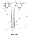
- FIGS. 8( a ) to 8 ( d ) are cross-sectional views illustrating a method for forming a MOSFET device according to an embodiment of the invention.
- FIG. 8( e ) shows a cross-sectional view of a MOSFET device with a stripe having a P ⁇ lining and a dielectric inner portion.
- the resistance of the epilayer in a MOSFET becomes an increasingly significant component of R DS(on) for increasing MOSFET voltage breakdown ratings.
- computer simulations have indicated that for a 30 volt N ⁇ channel trench MOSFET device, the epilayer resistance is about 30% or more of the total specific R DS(on) .
- the epilayer resistance is about 75 to 90% of the total specific R DS(on) .
- the reduction of R DS(on) preferably takes place without degrading the breakdown voltage characteristics of the MOSFET device.
- the maximum breakdown voltage (BV DSS ) of a trench or planar DMOSFET double diffused metal oxide semiconductor field effect transistor
- BV DSS maximum breakdown voltage
- the depletion region is formed by applying a reverse bias voltage across the junction.
- the reverse-biased epilayer/well diode breaks down and significant current starts to flow. Current flows between the source and drain by an avalanche multiplication process while the gate and the source are shorted together.
- FIGS. 1( a ) to 1 ( f ) show schematic cross-sectional views of a conventional vertical trench MOSFET device.
- Each cross-section shows a plurality of gate structures 45 at a major surface of a semiconductor substrate 29 .
- the semiconductor substrate 29 comprises an N ⁇ epilayer 32 and a drain region 31 .
- N+ source regions, P ⁇ wells, and P+ body regions are shown.
- N+ source regions and P+ body regions are not shown in FIGS. 1( b ) to 1 ( f ), 2 ( a ) to 2 ( f ), and 3 ( a ) to 3 ( f ).
- the N ⁇ epilayer 32 has a resistivity of about 5.0 ohm-cm and an epilayer dopant concentration, N d (epi), of about 1 ⁇ 10 15 cm ⁇ 3 .
- the thickness of the N ⁇ epilayer 32 is about 20 microns.
- the device also has an “effective” epilayer thickness (sometimes referred to as “effective epi”) of about 16.5 microns.
- the effective epilayer thickness is the thickness of the epilayer after taking into account any up diffusion of atoms from the N+ drain region 31 and the formation of regions such as doped regions (e.g., P ⁇ wells) in the semiconductor substrate 29 .
- the effective epilayer thickness can be substantially equal to the distance between the bottom of a P+ body or a P ⁇ well and the endpoint of any up-diffused donors in the N ⁇ epilayer 32 from the N+ substrate 31 .
- the effective epilayer for the device may also include the drift region for the device.
- FIGS. 1( a ) to 1 ( f ) also shows the maximum electric field established (“E max ”) as different reverse bias voltages are applied. As shown in the figures, as the reverse bias voltage is increased, E max also increases. If E max exceeds the critical electric field for a given dopant concentration, avalanche breakdown occurs. Consequently, E max is desirably less than the critical electric field.
- FIGS. 1( a ) to 1 ( f ) respectively show how the depletion region 50 expands as increasing reverse bias voltages of 0V, 10V, 50V, 100V, 200V, and 250V are applied to the conventional trench MOSFET device. As shown in the figures, as greater reverse bias voltages are applied, the depletion region 50 spreads “vertically” in a direction from the P ⁇ well/epilayer interface to the N+ drain region 31 . This vertical growth of the depletion region forces the trade-off between lower R DS(on) and higher BV DSS in conventional trench MOSFET devices.
- the present invention provides an improved MOSFET device wherein the depletion region initially spreads “horizontally” as higher reverse bias voltages are applied.
- a number of additional (and preferably deep) trenches are formed in the semiconductor substrate. These deep trenches are eventually used to form stripes that induce the formation of a horizontally spreading depletion region.
- the stripes comprise a material of the opposite type conductivity to the epilayer.
- the stripes may comprise a P type material (e.g., a P, P+, or P ⁇ silicon) while the epilayer may comprise an N type material.
- Individual stripes may be present between adjacent gate structures and can extend from the major surface of the semiconductor substrate and into the epilayer. The stripes can also extend any suitable distance into the epilayer.
- the stripes extend all the way to the epilayer/drain region interface.
- the presence of the stripes allows the use of a lower resistance epilayer without exceeding the critical electric field.
- R DS(on) can be reduced without detrimentally affecting other MOSFET device characteristics such as the breakdown voltage.
- FIGS. 2( a ) to 2 ( f ) illustrate an embodiment of the invention. These figures illustrate how a depletion region spreads as greater reverse bias voltages are applied.
- the gate bias voltages applied in the examples shown in FIGS. 2( a ) to 2 ( f ) are 0V, 1V, 2V, 10V, 200V, and 250V.
- each of the cross-sections of FIGS. 2( a ) to 2 ( f ) include a plurality of trench gate structures 45 and a N ⁇ epilayer 32 .
- the N ⁇ epilayer 32 is present in a semiconductor substrate 29 .
- a plurality of trenches forming stripes 35 (e.g., P stripes) of the opposite conductivity type as the N ⁇ epilayer 32 are respectively disposed between adjacent gate structures 45 .
- the stripes 35 comprise a P type material.
- the depletion region 50 initially spreads “horizontally” away from the sides of the stripes 35 .
- the regions between adjacent stripes 35 are quickly depleted of charge carriers as the depletion region 32 expands from the side-surfaces of adjacent stripes 35 .
- the depletion region 50 spreads vertically in a direction from the ends of the stripes 35 towards the N+ drain region 31 .
- the epilayer 32 in the embodiment is depleted of charge carriers much more quickly than when depletion initially occurs in a “vertical” manner (e.g., as shown in FIGS. 1( a ) to 1 ( f )).
- the depletion region 50 is similar in area with significantly less applied voltage (2V compared to 200 V).
- FIGS. 3( a ) to 3 ( f ) show cross sections of another MOSFET device according to another embodiment of the invention.
- like elements are denoted by like numerals in prior figures.
- the epilayer in the MOSFET device shown in FIG. 3( a ) has a resistivity of about 0.6 ohm-cm, a dopant concentration (N d ) of about 1 ⁇ 10 16 cm ⁇ 3 , a thickness of about 16 microns, and an effective epilayer thickness of about 12.5 microns.
- FIGS. 3( a ) to 3 ( f ) respectively show how the depletion region 50 changes at reverse bias voltages of 0V, 10V, 50V, 100V, 200V, and 250V.
- the depletion region 50 initially spreads “horizontally” as higher reverse bias voltages are applied.
- the maximum electric field (E max ) at each of these applied reverse bias voltages does not exceed the critical field for avalanche breakdown for the stated dopant concentration. Consequently, a high breakdown voltage (e.g., 250 V) can be obtained while using a thinner and lower resistivity.
- the thinner and lower resistivity epilayer advantageously results in a lower resistance epilayer and thus, a reduced R DS(on) value.
- the dimensions and doping level in the stripes 35 are adjusted to balance the total charge in the stripes with the total charge in the epilayer depletion region 50 .
- FIG. 4 shows a bar graph illustrating some components of R DS(on) for a number of N-channel MOSFET devices with different breakdown voltage ratings.
- Bar (a) represents the R DS(on) for a control N-channel 30 V MOSFET device at 500 A.
- Bars (b) to (f) refer to conventional trench N-channel MOSFET devices with respective breakdown voltages of 60, 80, 100, 150, and 200 V.
- the epilayer resistance has a greater impact on R DS(on) .
- the epilayer resistance constitutes over 90% of the total specific R DS(on) .
- the epilayer resistance has a significantly lower impact on R DS(on) .
- the epilayer resistance can be lowered by incorporating trenched stripes in the epilayer. This reduces R DS(on) as compared to a similar conventional MOSFET device with a similar breakdown voltage rating.
- bar (g) in FIG. 4 shows the improvement provided for a trench MOSFET device according to an exemplary embodiment of the invention.
- the epilayer resistance can be significantly reduced when using trenched stripes having the opposite conductivity of the epilayer in a MOSFET device.
- the total specific R DS(on) for a 200 V trench N-channel MOSFET device is less than 1.4 milliohm-cm 2 .
- the total specific R DS(on) is about 7.5 milliohm-cm 2 . Accordingly, these exemplary embodiments of the invention can exhibit a greater than 5-fold reduction in R DS(on) than conventional trench MOSFET devices.
- FIGS. 5 to 11 show graphs of reverse IV curves for MOSFET devices according to embodiments of the invention.
- FIG. 5 is a graph showing reverse IV curves for conventional trench MOSFET devices and a MOSFET device according to an embodiment of the invention.
- FIG. 5 shows IV curves 500 , 502 for two MOSFET devices without P ⁇ stripes.
- the first curve 500 is for a MOSFET device with an epilayer resistance of 0.8 milliohm-cm and an epilayer thickness of 15 microns.
- the second curve 502 is for a MOSFET device with an epilayer resistivity of 4.6 milliohm-cm and an epilayer thickness of 19.5 microns.
- the MOSFET device with the thicker epilayer and higher resistance has a higher breakdown voltage.
- An IV curve 504 for an embodiment of the invention is also shown in FIG. 5 .
- This exemplary embodiment has an epilayer resistance of about 0.8 ohm-cm, an epilayer thickness of about 15 microns and a P ⁇ stripe about 12 microns deep.
- this device embodiment has a relatively thin epilayer and a relatively low epilayer resistivity (and therefore a low R DS(on) . It also has a breakdown voltage approaching 220 V. The breakdown voltage is comparable to the breakdown voltage exhibited by a conventional MOSFET device having a thicker and more resistive epilayer.
- FIG. 6 shows reverse IV curves for MOSFET devices according to embodiments of the invention.
- the curves show the effect of varying the P ⁇ stripe depth on BV DSS .
- the epilayer has a resistance of about 0.8 ohm-cm and a thickness of about 13 microns.
- the P ⁇ stripe width is about 1.0 microns.
- the dopant concentration in the P ⁇ stripe is about 2.2 ⁇ 10 16 cm ⁇ 3 .
- the P ⁇ stripe depth was varied at about 8, 10, and 12, microns.
- the IV curves for these variations show that the breakdown voltage increases as the depth of the P ⁇ stripes is increased.
- FIG. 7 shows reverse IV curves for MOSFET devices according to embodiments of the invention.
- the curves show the effect of P ⁇ stripe width variations on BV DSS .
- the devices have an epilayer resistance of about 0.8 ohm-cm and a thickness of about 13 microns.
- the P ⁇ stripe depth is about 10 microns, and the dopant concentration in the P ⁇ stripe is about 2.2 ⁇ 10 16 cm ⁇ 3 .
- IV curves for P ⁇ stripes with widths of about 0.8, 1.0, and 1.2 microns are shown. The IV curves show that the breakdown voltage is higher when the width of the P ⁇ stripes is equal to 1 micron.
- Embodiments of the present invention can be applied to both trench and planar MOSFET technologies.
- trench MOSFET devices are preferred as they advantageously occupy less space than planar MOSFET devices.
- the breakdown voltage of the device may be from about 100 to about 400 volts in some embodiments.
- a method of manufacturing a MOSFET device according to the present invention is described below in the context of a trenched gate process.
- the power trench MOSFET device comprises a semiconductor substrate 29 having a drain region 31 and an N ⁇ epitaxial portion 32 proximate the drain region 31 .
- the semiconductor substrate 29 may comprise any suitable semiconductor material including Si, GaAs, etc.
- the drift region for the MOSFET device may be present in the epitaxial portion 32 of the semiconductor substrate 29 .
- a plurality of gate structures 45 are proximate the major surface 28 of the semiconductor substrate 29 , and each gate structure 45 comprises a gate electrode 43 and a dielectric layer 44 on the gate electrode 43 .
- a plurality of N+ source regions 36 are formed in the semiconductor substrate 29 .
- Each N+ source region 36 is adjacent to one of the gate structures 45 and is formed in a plurality of P ⁇ well regions 34 , which are also formed in the semiconductor substrate 29 .
- Each P ⁇ well region 34 is disposed adjacent to one of the gate structures 45 .
- a contact 41 for the source regions 36 is present on the major surface 28 of the semiconductor substrate 29 .
- the contact 41 may comprise a metal such as aluminum.
- other components which may be present in a MOSFET device e.g., a passivation layer may not be shown in FIG. 8( d ).
- a trenched P ⁇ stripe 35 is present in the semiconductor substrate 29 .
- a plurality of P ⁇ stripes 35 may be respectively disposed between adjacent gate structures 45 when the gate structures 45 form an array of gate structures 45 .
- the P ⁇ stripe 35 shown in FIG. 8( d ) is disposed between adjacent gate structures 45 .
- the P ⁇ stripe 35 shown in the figure is generally vertical and is oriented generally perpendicular to the orientation of the semiconductor substrate 29 .
- the P ⁇ stripe 35 extends past the gate structures 45 and may penetrate most of the N ⁇ epitaxial portion 32 .
- the N ⁇ epitaxial portion 32 in this embodiment surrounds the bottom and sides of the P ⁇ stripe 35 .
- the dopant concentration at the sides and below the P ⁇ stripe 35 may be similar in this embodiment.
- the P ⁇ stripe 35 has generally parallel sidewalls and a generally flat bottom. If the sidewalls are generally parallel, thin P ⁇ stripes 35 can be present between adjacent gate structures 45 .
- the pitch between gate structures 45 can be minimized consequently resulting in MOSFET arrays of reduced size.
- the gate structure 45 (or gate electrode) pitch may be less than about 10 microns (e.g., between about 4 to about 6 microns).
- the width of the P ⁇ stripes 35 may be less than about 2 or 3 microns (e.g., between about 1 and about 2 microns).
- the stripe trenches in embodiments of the invention are filled or lined with a material of the opposite doping to the epitaxial portion in the semiconductor substrate.
- An embodiment of this type is shown in FIG. 8( e ) and is described in greater detail below.
- the stripe may comprise an inner dielectric portion and an outer semiconductor layer of the opposite conductivity type as the epitaxial portion.
- the inner dielectric portion may comprise silicon oxide or air while the outer semiconductor layer may comprise P or N type epitaxial silicon.
- the presence of the doped stripes may also be used as a heavy body to improve the ruggedness of the formed device.
- the presence of P ⁇ stripes penetrating the epilayer is believed to stabilize voltage variations in the device, thus increasing the device's reliability.
- a structure including a semiconductor substrate 29 is provided.
- the semiconductor substrate 29 may comprise an N+ drain region 31 and an N ⁇ epitaxial portion 32 .
- Gate trenches 30 are formed proximate a major surface 28 of the semiconductor substrate 29 . These gate trenches 30 may be formed by using, for example, anisotropic etching methods well known in the art.
- gate structures 45 are formed within the gate trenches 30 using methods well known in the art.
- Each gate structure 45 comprises a dielectric layer 44 and a gate electrode 43 .
- the gate electrode 43 may comprise polysilicon and the dielectric layer 44 may comprise silicon dioxide.
- Source regions, well regions, and other structures may also be formed in the semiconductor substrate 29 after or before forming the gate structures 45 .
- P ⁇ well regions 34 are formed in the semiconductor substrate 29 and then N+ source regions 36 are formed in the semiconductor substrate 29 .
- Conventional ion implantation or conventional diffusion processes may be used to form these regions. In this example, these doped regions are formed after the formation of the gate structures 45 .
- one or more stripe trenches 30 are formed in the semiconductor substrate 29 .
- the stripe trench 30 shown in FIG. 8( c ) may be formed, e.g., by an anisotropic etching process.
- the formed stripe trench 30 extends from the major surface 28 of the semiconductor substrate 29 . It may extend any suitable distance past the gate structures 45 to the interface between the epitaxial portion 32 and the drain region 31 .
- the stripe trench 30 terminates at a depth which is between half the thickness of the N ⁇ epitaxial portion 32 and the full thickness of the epitaxial portion 32 .
- the stripe trench 30 may extend to the interface between the epitaxial portion 32 and the drain region 31 .
- a stripe 35 is formed in the stripe trench 30 .
- the stripe 35 comprises a material of the second conductivity type.
- the material of the second conductivity type is an epitaxial material such as epitaxial P type silicon (e.g., P, P+, P ⁇ silicon).
- the stripe trenches 30 may be filled using any suitable method including a selective epitaxial growth (SEG) process.
- the trenches 30 may be filled with epitaxial silicon with doping occurring in-situ.
- the material of the second conductivity type may completely fill the stripe trench 30 as shown in FIG. 8( d ) or may line the stripe trench 35 as shown in FIG. 8( e ).
- like numerals designate like elements as in FIG. 8( d ).
- the stripe 35 comprises a P ⁇ layer 35 ( a ) and an inner dielectric material 35 ( b ).
- the P ⁇ layer 35 ( a ) may be deposited in the formed stripe trench first, and then the dielectric material 35 ( b ) may be deposited to fill the enclosure formed by the P ⁇ layer 35 ( a ).
- the inner dielectric material may be formed by oxidizing the P ⁇ layer 35 ( a ).
- the dielectric material 35 ( b ) may comprise a material such as silicon dioxide or air.
- the stripe trench 30 and the stripes 35 of a second conductivity type are preferably formed after at least one of the source regions 36 , the gate structures 45 , and the well regions 34 are formed.
- the stripes 35 are not subjected to the high temperature processing used to form the gate structures 45 or the P ⁇ well regions 34 .
- the high temperature processing e.g., ion implantation, high temperature drives
- the P ⁇ well regions can last as long as 1 to 3 hours at high temperatures (e.g., greater than 1100° C.).
- the formation of the P ⁇ stripes 35 in the semiconductor substrate 29 does not detrimentally affect previously formed gate structures 45 , P ⁇ well regions 34 , or the N+ source regions 36 .
- Forming these device elements before forming the P ⁇ stripes 35 reduces the likelihood that the P ⁇ stripes 35 in the epilayer will diffuse and lose their shape due to extended high temperature processing. If this occurs, the width of the P ⁇ stripes 35 may not be uniform down the P ⁇ stripe 35 and may decrease the effectiveness of the formed device. For example, dopant from a laterally enlarged P ⁇ stripe 35 could diffuse into the channel region of the MOSFET device thereby influencing the threshold voltage characteristics of the MOSFET device. Moreover, wider P ⁇ stripes can result in a larger gate structure 45 pitch, thus increasing the size of a corresponding array of gate structures 45 .
- Additional layers may include a metal contact layer 41 and a passivation layer (not shown). These additional layers may be formed by any suitable method known in the art.
- embodiments of the invention are not limited thereto.
- embodiments of the invention have been described with reference to N type semiconductors, P ⁇ stripes, etc. It is understood that the invention is not limited thereto and that the doping polarities of the structures shown and described could be reversed.
- P ⁇ stripes are mentioned in detail, it is understood that the stripes used in embodiments of the invention may be P or N type.
- the stripes or other device elements may also have any suitable acceptor or donor concentration (e.g., +, ++, ⁇ , ⁇ , etc.).
Abstract
Description
Claims (9)
Priority Applications (1)
| Application Number | Priority Date | Filing Date | Title |
|---|---|---|---|
| US12/893,997 US8829641B2 (en) | 2001-01-30 | 2010-09-29 | Method of forming a dual-trench field effect transistor |
Applications Claiming Priority (4)
| Application Number | Priority Date | Filing Date | Title |
|---|---|---|---|
| US09/774,780 US6713813B2 (en) | 2001-01-30 | 2001-01-30 | Field effect transistor having a lateral depletion structure |
| US10/741,464 US6818513B2 (en) | 2001-01-30 | 2003-12-18 | Method of forming a field effect transistor having a lateral depletion structure |
| US10/934,969 US20050029618A1 (en) | 2001-01-30 | 2004-09-03 | Structure and method of forming a dual-trench field effect transistor |
| US12/893,997 US8829641B2 (en) | 2001-01-30 | 2010-09-29 | Method of forming a dual-trench field effect transistor |
Related Parent Applications (1)
| Application Number | Title | Priority Date | Filing Date |
|---|---|---|---|
| US10/934,969 Division US20050029618A1 (en) | 2001-01-30 | 2004-09-03 | Structure and method of forming a dual-trench field effect transistor |
Publications (2)
| Publication Number | Publication Date |
|---|---|
| US20110014764A1 US20110014764A1 (en) | 2011-01-20 |
| US8829641B2 true US8829641B2 (en) | 2014-09-09 |
Family
ID=25102275
Family Applications (3)
| Application Number | Title | Priority Date | Filing Date |
|---|---|---|---|
| US10/741,464 Expired - Lifetime US6818513B2 (en) | 2001-01-30 | 2003-12-18 | Method of forming a field effect transistor having a lateral depletion structure |
| US10/934,969 Abandoned US20050029618A1 (en) | 2001-01-30 | 2004-09-03 | Structure and method of forming a dual-trench field effect transistor |
| US12/893,997 Expired - Lifetime US8829641B2 (en) | 2001-01-30 | 2010-09-29 | Method of forming a dual-trench field effect transistor |
Family Applications Before (2)
| Application Number | Title | Priority Date | Filing Date |
|---|---|---|---|
| US10/741,464 Expired - Lifetime US6818513B2 (en) | 2001-01-30 | 2003-12-18 | Method of forming a field effect transistor having a lateral depletion structure |
| US10/934,969 Abandoned US20050029618A1 (en) | 2001-01-30 | 2004-09-03 | Structure and method of forming a dual-trench field effect transistor |
Country Status (1)
| Country | Link |
|---|---|
| US (3) | US6818513B2 (en) |
Cited By (5)
| Publication number | Priority date | Publication date | Assignee | Title |
|---|---|---|---|---|
| US20140284703A1 (en) * | 2013-03-21 | 2014-09-25 | Silergy Semiconductor Technology (Hangzhou) Ltd | Vertical double-diffusion mos and manufacturing technique for the same |
| US20180190805A1 (en) * | 2015-11-10 | 2018-07-05 | ZhuZhou CRRC Times Electric Co., Ltd. | Insulated gate bipolar transistor and preparation method therefor |
| US20210184009A1 (en) * | 2019-12-17 | 2021-06-17 | Silergy Semiconductor Technology (Hangzhou) Ltd | Trench mosfet and method for manufacturing the same |
| US11424344B2 (en) | 2019-11-22 | 2022-08-23 | Hangzhou Silicon-Magic Semiconductor Technology Co., Ltd. | Trench MOSFET and method for manufacturing the same |
| US11670502B2 (en) | 2020-04-23 | 2023-06-06 | Hangzhou Silicon-Magic Semiconductor Technology Co., Ltd. | SiC MOSFET and method for manufacturing the same |
Families Citing this family (23)
| Publication number | Priority date | Publication date | Assignee | Title |
|---|---|---|---|---|
| US6818513B2 (en) | 2001-01-30 | 2004-11-16 | Fairchild Semiconductor Corporation | Method of forming a field effect transistor having a lateral depletion structure |
| US7652326B2 (en) | 2003-05-20 | 2010-01-26 | Fairchild Semiconductor Corporation | Power semiconductor devices and methods of manufacture |
| US7019358B2 (en) * | 2003-07-31 | 2006-03-28 | Clare, Inc. | High voltage semiconductor device having an increased breakdown voltage relative to its on-resistance |
| US7268395B2 (en) * | 2004-06-04 | 2007-09-11 | International Rectifier Corporation | Deep trench super switch device |
| US7352036B2 (en) | 2004-08-03 | 2008-04-01 | Fairchild Semiconductor Corporation | Semiconductor power device having a top-side drain using a sinker trench |
| KR101279574B1 (en) * | 2006-11-15 | 2013-06-27 | 페어차일드코리아반도체 주식회사 | High voltage semiconductor device and method of fabricating the same |
| WO2008106235A1 (en) * | 2007-03-01 | 2008-09-04 | International Rectifier Corporation | Trench mosgated device with deep trench between gate trenches |
| CN103762243B (en) | 2007-09-21 | 2017-07-28 | 飞兆半导体公司 | Power device |
| US7880224B2 (en) * | 2008-01-25 | 2011-02-01 | Infineon Technologies Austria Ag | Semiconductor component having discontinuous drift zone control dielectric arranged between drift zone and drift control zone and a method of making the same |
| US20120273916A1 (en) | 2011-04-27 | 2012-11-01 | Yedinak Joseph A | Superjunction Structures for Power Devices and Methods of Manufacture |
| US9508805B2 (en) | 2008-12-31 | 2016-11-29 | Alpha And Omega Semiconductor Incorporated | Termination design for nanotube MOSFET |
| US7943989B2 (en) * | 2008-12-31 | 2011-05-17 | Alpha And Omega Semiconductor Incorporated | Nano-tube MOSFET technology and devices |
| US8299494B2 (en) * | 2009-06-12 | 2012-10-30 | Alpha & Omega Semiconductor, Inc. | Nanotube semiconductor devices |
| US7910486B2 (en) * | 2009-06-12 | 2011-03-22 | Alpha & Omega Semiconductor, Inc. | Method for forming nanotube semiconductor devices |
| US8129778B2 (en) * | 2009-12-02 | 2012-03-06 | Fairchild Semiconductor Corporation | Semiconductor devices and methods for making the same |
| US20110198689A1 (en) * | 2010-02-17 | 2011-08-18 | Suku Kim | Semiconductor devices containing trench mosfets with superjunctions |
| CN102751190B (en) * | 2011-04-22 | 2014-12-03 | 科轩微电子股份有限公司 | Channel type power metal oxide semi-conductor structure with fast switching capacity and manufacture method |
| US8772868B2 (en) | 2011-04-27 | 2014-07-08 | Fairchild Semiconductor Corporation | Superjunction structures for power devices and methods of manufacture |
| US8836028B2 (en) | 2011-04-27 | 2014-09-16 | Fairchild Semiconductor Corporation | Superjunction structures for power devices and methods of manufacture |
| US8673700B2 (en) * | 2011-04-27 | 2014-03-18 | Fairchild Semiconductor Corporation | Superjunction structures for power devices and methods of manufacture |
| US8786010B2 (en) | 2011-04-27 | 2014-07-22 | Fairchild Semiconductor Corporation | Superjunction structures for power devices and methods of manufacture |
| US20150118810A1 (en) * | 2013-10-24 | 2015-04-30 | Madhur Bobde | Buried field ring field effect transistor (buf-fet) integrated with cells implanted with hole supply path |
| US9484404B2 (en) | 2014-01-29 | 2016-11-01 | Stmicroelectronics S.R.L. | Electronic device of vertical MOS type with termination trenches having variable depth |
Citations (266)
| Publication number | Priority date | Publication date | Assignee | Title |
|---|---|---|---|---|
| US3404295A (en) | 1964-11-30 | 1968-10-01 | Motorola Inc | High frequency and voltage transistor with added region for punch-through protection |
| US3412297A (en) | 1965-12-16 | 1968-11-19 | United Aircraft Corp | Mos field-effect transistor with a onemicron vertical channel |
| US3497777A (en) | 1967-06-13 | 1970-02-24 | Stanislas Teszner | Multichannel field-effect semi-conductor device |
| US3564356A (en) | 1968-10-24 | 1971-02-16 | Tektronix Inc | High voltage integrated circuit transistor |
| US3660697A (en) | 1970-02-16 | 1972-05-02 | Bell Telephone Labor Inc | Monolithic semiconductor apparatus adapted for sequential charge transfer |
| US4003072A (en) | 1972-04-20 | 1977-01-11 | Sony Corporation | Semiconductor device with high voltage breakdown resistance |
| US4300150A (en) | 1980-06-16 | 1981-11-10 | North American Philips Corporation | Lateral double-diffused MOS transistor device |
| US4326332A (en) | 1980-07-28 | 1982-04-27 | International Business Machines Corp. | Method of making a high density V-MOS memory array |
| US4337474A (en) | 1978-08-31 | 1982-06-29 | Mitsubishi Denki Kabushiki Kaisha | Semiconductor device |
| US4345265A (en) | 1980-04-14 | 1982-08-17 | Supertex, Inc. | MOS Power transistor with improved high-voltage capability |
| US4445202A (en) | 1980-11-12 | 1984-04-24 | International Business Machines Corporation | Electrically switchable permanent storage |
| US4579621A (en) | 1983-07-08 | 1986-04-01 | Mitsubishi Denki Kabushiki Kaisha | Selective epitaxial growth method |
| US4636281A (en) | 1984-06-14 | 1987-01-13 | Commissariat A L'energie Atomique | Process for the autopositioning of a local field oxide with respect to an insulating trench |
| US4638344A (en) | 1979-10-09 | 1987-01-20 | Cardwell Jr Walter T | Junction field-effect transistor controlled by merged depletion regions |
| US4639761A (en) | 1983-12-16 | 1987-01-27 | North American Philips Corporation | Combined bipolar-field effect transistor resurf devices |
| US4698653A (en) | 1979-10-09 | 1987-10-06 | Cardwell Jr Walter T | Semiconductor devices controlled by depletion regions |
| US4716126A (en) | 1986-06-05 | 1987-12-29 | Siliconix Incorporated | Fabrication of double diffused metal oxide semiconductor transistor |
| US4746630A (en) | 1986-09-17 | 1988-05-24 | Hewlett-Packard Company | Method for producing recessed field oxide with improved sidewall characteristics |
| US4754310A (en) | 1980-12-10 | 1988-06-28 | U.S. Philips Corp. | High voltage semiconductor device |
| US4774556A (en) | 1985-07-25 | 1988-09-27 | Nippondenso Co., Ltd. | Non-volatile semiconductor memory device |
| US4801986A (en) | 1987-04-03 | 1989-01-31 | General Electric Company | Vertical double diffused metal oxide semiconductor VDMOS device with increased safe operating area and method |
| US4821095A (en) | 1987-03-12 | 1989-04-11 | General Electric Company | Insulated gate semiconductor device with extra short grid and method of fabrication |
| US4823176A (en) | 1987-04-03 | 1989-04-18 | General Electric Company | Vertical double diffused metal oxide semiconductor (VDMOS) device including high voltage junction exhibiting increased safe operating area |
| US4853345A (en) | 1988-08-22 | 1989-08-01 | Delco Electronics Corporation | Process for manufacture of a vertical DMOS transistor |
| US4868624A (en) | 1980-05-09 | 1989-09-19 | Regents Of The University Of Minnesota | Channel collector transistor |
| CN1036666A (en) | 1988-02-22 | 1989-10-25 | 亚瑞亚·勃朗·勃威力有限公司 | The bipolar-type power semiconductor device and the manufacture method thereof of field effect control |
| US4893160A (en) | 1987-11-13 | 1990-01-09 | Siliconix Incorporated | Method for increasing the performance of trenched devices and the resulting structure |
| US4914058A (en) | 1987-12-29 | 1990-04-03 | Siliconix Incorporated | Grooved DMOS process with varying gate dielectric thickness |
| US4941026A (en) | 1986-12-05 | 1990-07-10 | General Electric Company | Semiconductor devices exhibiting minimum on-resistance |
| US4967245A (en) | 1988-03-14 | 1990-10-30 | Siliconix Incorporated | Trench power MOSFET device |
| US4974059A (en) | 1982-12-21 | 1990-11-27 | International Rectifier Corporation | Semiconductor high-power mosfet device |
| US4990463A (en) | 1988-07-05 | 1991-02-05 | Kabushiki Kaisha Toshiba | Method of manufacturing capacitor |
| US4992390A (en) | 1989-07-06 | 1991-02-12 | General Electric Company | Trench gate structure with thick bottom oxide |
| US5027180A (en) | 1986-12-11 | 1991-06-25 | Mitsubishi Electric Corporation | Double gate static induction thyristor |
| US5034785A (en) | 1986-03-24 | 1991-07-23 | Siliconix Incorporated | Planar vertical channel DMOS structure |
| US5071782A (en) | 1990-06-28 | 1991-12-10 | Texas Instruments Incorporated | Vertical memory cell array and method of fabrication |
| US5072266A (en) | 1988-12-27 | 1991-12-10 | Siliconix Incorporated | Trench DMOS power transistor with field-shaping body profile and three-dimensional geometry |
| US5079608A (en) | 1990-11-06 | 1992-01-07 | Harris Corporation | Power MOSFET transistor circuit with active clamp |
| US5105243A (en) | 1987-02-26 | 1992-04-14 | Kabushiki Kaisha Toshiba | Conductivity-modulation metal oxide field effect transistor with single gate structure |
| US5111253A (en) | 1989-05-09 | 1992-05-05 | General Electric Company | Multicellular FET having a Schottky diode merged therewith |
| US5142640A (en) | 1988-06-02 | 1992-08-25 | Seiko Epson Corporation | Trench gate metal oxide semiconductor field effect transistor |
| US5164325A (en) | 1987-10-08 | 1992-11-17 | Siliconix Incorporated | Method of making a vertical current flow field effect transistor |
| US5164802A (en) | 1991-03-20 | 1992-11-17 | Harris Corporation | Power vdmosfet with schottky on lightly doped drain of lateral driver fet |
| US5216275A (en) | 1991-03-19 | 1993-06-01 | University Of Electronic Science And Technology Of China | Semiconductor power devices with alternating conductivity type high-voltage breakdown regions |
| US5219793A (en) | 1991-06-03 | 1993-06-15 | Motorola Inc. | Method for forming pitch independent contacts and a semiconductor device having the same |
| US5219777A (en) | 1991-06-14 | 1993-06-15 | Gold Star Electron Co., Ltd. | Metal oxide semiconductor field effect transistor and method of making the same |
| US5233215A (en) | 1992-06-08 | 1993-08-03 | North Carolina State University At Raleigh | Silicon carbide power MOSFET with floating field ring and floating field plate |
| US5262336A (en) | 1986-03-21 | 1993-11-16 | Advanced Power Technology, Inc. | IGBT process to produce platinum lifetime control |
| US5268311A (en) | 1988-09-01 | 1993-12-07 | International Business Machines Corporation | Method for forming a thin dielectric layer on a substrate |
| DE4300806C1 (en) | 1993-01-14 | 1993-12-23 | Siemens Ag | Vertical MOS transistor prodn. - with reduced trench spacing, without parasitic bipolar effects |
| US5275965A (en) | 1992-11-25 | 1994-01-04 | Micron Semiconductor, Inc. | Trench isolation using gated sidewalls |
| US5294824A (en) | 1992-07-31 | 1994-03-15 | Motorola, Inc. | High voltage transistor having reduced on-resistance |
| US5300447A (en) | 1992-09-29 | 1994-04-05 | Texas Instruments Incorporated | Method of manufacturing a minimum scaled transistor |
| US5326711A (en) | 1993-01-04 | 1994-07-05 | Texas Instruments Incorporated | High performance high voltage vertical transistor and method of fabrication |
| US5350937A (en) | 1991-10-08 | 1994-09-27 | Semiconductor Energy Laboratory Co., Ltd. | Non-volatile memory device having a floating gate |
| US5365102A (en) | 1993-07-06 | 1994-11-15 | North Carolina State University | Schottky barrier rectifier with MOS trench |
| US5366914A (en) | 1992-01-29 | 1994-11-22 | Nec Corporation | Vertical power MOSFET structure having reduced cell area |
| US5389815A (en) | 1992-04-28 | 1995-02-14 | Mitsubishi Denki Kabushiki Kaisha | Semiconductor diode with reduced recovery current |
| US5405794A (en) | 1994-06-14 | 1995-04-11 | Philips Electronics North America Corporation | Method of producing VDMOS device of increased power density |
| US5418376A (en) | 1993-03-02 | 1995-05-23 | Toyo Denki Seizo Kabushiki Kaisha | Static induction semiconductor device with a distributed main electrode structure and static induction semiconductor device with a static induction main electrode shorted structure |
| US5424231A (en) | 1994-08-09 | 1995-06-13 | United Microelectronics Corp. | Method for manufacturing a VDMOS transistor |
| US5430324A (en) | 1992-07-23 | 1995-07-04 | Siliconix, Incorporated | High voltage transistor having edge termination utilizing trench technology |
| US5430311A (en) | 1991-09-20 | 1995-07-04 | Hitachi, Ltd. | Constant-voltage diode for over-voltage protection |
| US5429977A (en) | 1994-03-11 | 1995-07-04 | Industrial Technology Research Institute | Method for forming a vertical transistor with a stacked capacitor DRAM cell |
| US5434435A (en) | 1994-05-04 | 1995-07-18 | North Carolina State University | Trench gate lateral MOSFET |
| US5436189A (en) | 1989-10-03 | 1995-07-25 | Harris Corporation | Self-aligned channel stop for trench-isolated island |
| US5438215A (en) | 1993-03-25 | 1995-08-01 | Siemens Aktiengesellschaft | Power MOSFET |
| US5473180A (en) | 1993-07-12 | 1995-12-05 | U.S. Philips Corporation | Semiconductor device with an MOST provided with an extended drain region for high voltages |
| US5473176A (en) | 1993-09-01 | 1995-12-05 | Kabushiki Kaisha Toshiba | Vertical insulated gate transistor and method of manufacture |
| US5474943A (en) | 1993-03-15 | 1995-12-12 | Siliconix Incorporated | Method for fabricating a short channel trenched DMOS transistor |
| US5519245A (en) | 1989-08-31 | 1996-05-21 | Nippondenso Co., Ltd. | Insulated gate bipolar transistor with reverse conducting current |
| US5541425A (en) | 1994-01-20 | 1996-07-30 | Mitsubishi Denki Kabushiki Kaisha | Semiconductor device having trench structure |
| US5554862A (en) | 1992-03-31 | 1996-09-10 | Kabushiki Kaisha Toshiba | Power semiconductor device |
| US5567635A (en) | 1992-03-23 | 1996-10-22 | International Business Machines Corporation | Method of making a three dimensional trench EEPROM cell structure |
| US5567634A (en) | 1995-05-01 | 1996-10-22 | National Semiconductor Corporation | Method of fabricating self-aligned contact trench DMOS transistors |
| US5572048A (en) | 1992-11-20 | 1996-11-05 | Hitachi, Ltd. | Voltage-driven type semiconductor device |
| US5578851A (en) | 1994-08-15 | 1996-11-26 | Siliconix Incorporated | Trenched DMOS transistor having thick field oxide in termination region |
| US5581100A (en) | 1994-08-30 | 1996-12-03 | International Rectifier Corporation | Trench depletion MOSFET |
| US5583065A (en) | 1994-11-23 | 1996-12-10 | Sony Corporation | Method of making a MOS semiconductor device |
| US5592005A (en) | 1995-03-31 | 1997-01-07 | Siliconix Incorporated | Punch-through field effect transistor |
| US5595927A (en) | 1995-03-17 | 1997-01-21 | Taiwan Semiconductor Manufacturing Company Ltd. | Method for making self-aligned source/drain mask ROM memory cell using trench etched channel |
| US5597765A (en) | 1995-01-10 | 1997-01-28 | Siliconix Incorporated | Method for making termination structure for power MOSFET |
| US5616945A (en) | 1995-10-13 | 1997-04-01 | Siliconix Incorporated | Multiple gated MOSFET for use in DC-DC converter |
| US5623152A (en) | 1995-02-09 | 1997-04-22 | Mitsubishi Denki Kabushiki Kaisha | Insulated gate semiconductor device |
| US5629543A (en) | 1995-08-21 | 1997-05-13 | Siliconix Incorporated | Trenched DMOS transistor with buried layer for reduced on-resistance and ruggedness |
| US5637898A (en) | 1995-12-22 | 1997-06-10 | North Carolina State University | Vertical field effect transistors having improved breakdown voltage capability and low on-state resistance |
| US5640034A (en) | 1992-05-18 | 1997-06-17 | Texas Instruments Incorporated | Top-drain trench based resurf DMOS transistor structure |
| US5648670A (en) | 1995-06-07 | 1997-07-15 | Sgs-Thomson Microelectronics, Inc. | Trench MOS-gated device with a minimum number of masks |
| US5656843A (en) | 1992-08-05 | 1997-08-12 | U.S. Philips Corporation | Semiconductor device having a vertical insulated gate field effect device and a breakdown region remote from the gate |
| US5670803A (en) | 1995-02-08 | 1997-09-23 | International Business Machines Corporation | Three-dimensional SRAM trench structure and fabrication method therefor |
| US5689128A (en) | 1995-08-21 | 1997-11-18 | Siliconix Incorporated | High density trenched DMOS transistor |
| US5693569A (en) | 1995-01-26 | 1997-12-02 | Fuji Electric Co., Ltd. | Method of forming silicon carbide trench mosfet with a schottky electrode |
| US5705409A (en) | 1995-09-28 | 1998-01-06 | Motorola Inc. | Method for forming trench transistor structure |
| US5710072A (en) | 1994-05-17 | 1998-01-20 | Siemens Aktiengesellschaft | Method of producing and arrangement containing self-amplifying dynamic MOS transistor memory cells |
| US5714781A (en) | 1995-04-27 | 1998-02-03 | Nippondenso Co., Ltd. | Semiconductor device having a gate electrode in a grove and a diffused region under the grove |
| US5719409A (en) | 1996-06-06 | 1998-02-17 | Cree Research, Inc. | Silicon carbide metal-insulator semiconductor field effect transistor |
| US5770878A (en) | 1996-04-10 | 1998-06-23 | Harris Corporation | Trench MOS gate device |
| US5776813A (en) | 1997-10-06 | 1998-07-07 | Industrial Technology Research Institute | Process to manufacture a vertical gate-enhanced bipolar transistor |
| US5780343A (en) | 1995-12-20 | 1998-07-14 | National Semiconductor Corporation | Method of producing high quality silicon surface for selective epitaxial growth of silicon |
| DE19736981A1 (en) | 1997-02-10 | 1998-08-20 | Mitsubishi Electric Corp | Semiconductor component of low loss and high breakdown voltage |
| US5801417A (en) | 1988-05-17 | 1998-09-01 | Advanced Power Technology, Inc. | Self-aligned power MOSFET device with recessed gate and source |
| US5877528A (en) | 1997-03-03 | 1999-03-02 | Megamos Corporation | Structure to provide effective channel-stop in termination areas for trenched power transistors |
| US5879994A (en) | 1997-04-15 | 1999-03-09 | National Semiconductor Corporation | Self-aligned method of fabricating terrace gate DMOS transistor |
| US5879971A (en) | 1995-09-28 | 1999-03-09 | Motorola Inc. | Trench random access memory cell and method of formation |
| US5895951A (en) | 1996-04-05 | 1999-04-20 | Megamos Corporation | MOSFET structure and fabrication process implemented by forming deep and narrow doping regions through doping trenches |
| US5895952A (en) | 1994-12-30 | 1999-04-20 | Siliconix Incorporated | Trench MOSFET with multi-resistivity drain to provide low on-resistance |
| US5897343A (en) | 1998-03-30 | 1999-04-27 | Motorola, Inc. | Method of making a power switching trench MOSFET having aligned source regions |
| US5897360A (en) | 1996-10-21 | 1999-04-27 | Nec Corporation | Manufacturing method of semiconductor integrated circuit |
| US5900663A (en) | 1998-02-07 | 1999-05-04 | Xemod, Inc. | Quasi-mesh gate structure for lateral RF MOS devices |
| US5906680A (en) | 1986-09-12 | 1999-05-25 | International Business Machines Corporation | Method and apparatus for low temperature, low pressure chemical vapor deposition of epitaxial silicon layers |
| US5917216A (en) | 1995-02-10 | 1999-06-29 | Siliconix Incorporated | Trenched field effect transistor with PN depletion barrier |
| US5929481A (en) | 1996-07-19 | 1999-07-27 | Siliconix Incorporated | High density trench DMOS transistor with trench bottom implant |
| US5943581A (en) | 1997-11-05 | 1999-08-24 | Vanguard International Semiconductor Corporation | Method of fabricating a buried reservoir capacitor structure for high-density dynamic random access memory (DRAM) circuits |
| US5949104A (en) | 1998-02-07 | 1999-09-07 | Xemod, Inc. | Source connection structure for lateral RF MOS devices |
| US5949124A (en) | 1995-10-31 | 1999-09-07 | Motorola, Inc. | Edge termination structure |
| US5959324A (en) | 1992-03-30 | 1999-09-28 | Kabushiki Kaisha Toshiba | Semiconductor device including an improved terminal structure |
| US5960271A (en) | 1996-09-18 | 1999-09-28 | Advanced Micro Devices, Inc. | Short channel self-aligned VMOS field effect transistor |
| US5973367A (en) | 1995-10-13 | 1999-10-26 | Siliconix Incorporated | Multiple gated MOSFET for use in DC-DC converter |
| US5973360A (en) | 1996-03-20 | 1999-10-26 | Siemens Aktiengesellschaft | Field effect-controllable semiconductor component |
| US5972741A (en) | 1996-10-31 | 1999-10-26 | Sanyo Electric Co., Ltd. | Method of manufacturing semiconductor device |
| US5976936A (en) | 1995-09-06 | 1999-11-02 | Denso Corporation | Silicon carbide semiconductor device |
| US5981996A (en) | 1995-02-17 | 1999-11-09 | Fuji Electric Co., Ltd. | Vertical trench misfet and method of manufacturing the same |
| US5981344A (en) | 1992-07-24 | 1999-11-09 | Siliconix Incorporated | Trench field effect transistor with reduced punch-through susceptibility and low RDSon |
| US5998833A (en) | 1998-10-26 | 1999-12-07 | North Carolina State University | Power semiconductor devices having improved high frequency switching and breakdown characteristics |
| US6005271A (en) | 1997-11-05 | 1999-12-21 | Magepower Semiconductor Corp. | Semiconductor cell array with high packing density |
| US6008097A (en) | 1996-12-14 | 1999-12-28 | Electronics And Telecommunications Research Institute | MOS transistor of semiconductor device and method of manufacturing the same |
| US6011298A (en) | 1996-12-31 | 2000-01-04 | Stmicroelectronics, Inc. | High voltage termination with buried field-shaping region |
| US6015727A (en) | 1998-06-08 | 2000-01-18 | Wanlass; Frank M. | Damascene formation of borderless contact MOS transistors |
| US6020250A (en) | 1994-08-11 | 2000-02-01 | International Business Machines Corporation | Stacked devices |
| JP2000040822A (en) | 1998-07-24 | 2000-02-08 | Fuji Electric Co Ltd | Superjunction semiconductor element and its manufacture |
| JP2000040872A (en) | 1998-07-24 | 2000-02-08 | Senju Metal Ind Co Ltd | Method of soldering printed board, and jet solder vessel |
| US6037628A (en) | 1997-06-30 | 2000-03-14 | Intersil Corporation | Semiconductor structures with trench contacts |
| US6037632A (en) | 1995-11-06 | 2000-03-14 | Kabushiki Kaisha Toshiba | Semiconductor device |
| US6048772A (en) | 1998-05-04 | 2000-04-11 | Xemod, Inc. | Method for fabricating a lateral RF MOS device with an non-diffusion source-backside connection |
| US6049108A (en) | 1995-06-02 | 2000-04-11 | Siliconix Incorporated | Trench-gated MOSFET with bidirectional voltage clamping |
| US6057558A (en) | 1997-03-05 | 2000-05-02 | Denson Corporation | Silicon carbide semiconductor device and manufacturing method thereof |
| US6063678A (en) | 1998-05-04 | 2000-05-16 | Xemod, Inc. | Fabrication of lateral RF MOS devices with enhanced RF properties |
| US6064088A (en) | 1998-06-15 | 2000-05-16 | Xemod, Inc. | RF power MOSFET device with extended linear region of transconductance characteristic at low drain current |
| US6066878A (en) | 1997-11-10 | 2000-05-23 | Intersil Corporation | High voltage semiconductor structure |
| JP2000156978A (en) | 1998-11-17 | 2000-06-06 | Fuji Electric Co Ltd | Soft switching circuit |
| WO2000033386A2 (en) | 1998-11-28 | 2000-06-08 | Koninklijke Philips Electronics N.V. | Trench-gate semiconductor devices and their manufacture |
| US6084264A (en) | 1998-11-25 | 2000-07-04 | Siliconix Incorporated | Trench MOSFET having improved breakdown and on-resistance characteristics |
| US6084268A (en) | 1996-03-05 | 2000-07-04 | Semiconductor Components Industries, Llc | Power MOSFET device having low on-resistance and method |
| US6087232A (en) | 1997-10-28 | 2000-07-11 | Electronics And Telecommunications Research Institute | Fabrication method of lateral double diffused MOS transistors |
| US6096608A (en) | 1997-06-30 | 2000-08-01 | Siliconix Incorporated | Bidirectional trench gated power mosfet with submerged body bus extending underneath gate trench |
| US6097063A (en) | 1996-01-22 | 2000-08-01 | Fuji Electric Co., Ltd. | Semiconductor device having a plurality of parallel drift regions |
| EP1026749A1 (en) | 1998-07-23 | 2000-08-09 | Mitsubishi Denki Kabushiki Kaisha | Semiconductor device and method for fabricating the same |
| US6104054A (en) | 1998-05-13 | 2000-08-15 | Texas Instruments Incorporated | Space-efficient layout method to reduce the effect of substrate capacitance in dielectrically isolated process technologies |
| US6110799A (en) | 1997-06-30 | 2000-08-29 | Intersil Corporation | Trench contact process |
| US6114727A (en) | 1997-01-09 | 2000-09-05 | Kabushiki Kaisha Toshiba | Semiconductor device |
| JP2000277728A (en) | 1999-03-25 | 2000-10-06 | Nec Kansai Ltd | Insulated-gate semiconductor device and its manufacture |
| JP2000277726A (en) | 1999-03-23 | 2000-10-06 | Toshiba Corp | High breakdown strength semiconductor element |
| US6137152A (en) | 1998-04-22 | 2000-10-24 | Texas Instruments - Acer Incorporated | Planarized deep-shallow trench isolation for CMOS/bipolar devices |
| WO2000068998A1 (en) | 1999-05-06 | 2000-11-16 | C.P. Clare Corporation | High voltage mosfet structures |
| WO2000068997A1 (en) | 1999-05-06 | 2000-11-16 | C.P. Clare Corporation | Mosfet with field reducing trenches in body region |
| US6150697A (en) | 1998-04-30 | 2000-11-21 | Denso Corporation | Semiconductor apparatus having high withstand voltage |
| EP1054451A2 (en) | 1999-05-19 | 2000-11-22 | Intersil Corporation | MOS-gated power device having extended trench and doping zone and process for forming same |
| US6156611A (en) | 1998-07-20 | 2000-12-05 | Motorola, Inc. | Method of fabricating vertical FET with sidewall gate electrode |
| US6156606A (en) | 1998-11-17 | 2000-12-05 | Siemens Aktiengesellschaft | Method of forming a trench capacitor using a rutile dielectric material |
| US6163052A (en) | 1997-04-04 | 2000-12-19 | Advanced Micro Devices, Inc. | Trench-gated vertical combination JFET and MOSFET devices |
| US6165870A (en) | 1998-06-30 | 2000-12-26 | Hyundai Electronics Industries Co., Ltd. | Element isolation method for semiconductor devices including etching implanted region under said spacer to form a stepped trench structure |
| US6168983B1 (en) | 1996-11-05 | 2001-01-02 | Power Integrations, Inc. | Method of making a high-voltage transistor with multiple lateral conduction layers |
| US6168996B1 (en) | 1997-08-28 | 2001-01-02 | Hitachi, Ltd. | Method of fabricating semiconductor device |
| US6171935B1 (en) | 1998-05-06 | 2001-01-09 | Siemens Aktiengesellschaft | Process for producing an epitaxial layer with laterally varying doping |
| US6174785B1 (en) | 1998-04-09 | 2001-01-16 | Micron Technology, Inc. | Method of forming trench isolation region for semiconductor device |
| JP2001015752A (en) | 1998-11-11 | 2001-01-19 | Fuji Electric Co Ltd | Superjunction semiconductor element and manufacture thereof |
| JP2001015448A (en) | 1999-06-28 | 2001-01-19 | Toshiba Corp | Manufacture of semiconductor device |
| WO2001006557A1 (en) | 1999-07-14 | 2001-01-25 | Koninklijke Philips Electronics N.V. | Method of making a charge compensation semiconductor device using neutron transmutation |
| WO2001006550A1 (en) | 1999-07-15 | 2001-01-25 | Koninklijke Philips Electronics N.V. | Method of making a charge compensation semiconductor device using direct bonding and corresponding device |
| US6184545B1 (en) | 1997-09-12 | 2001-02-06 | Infineon Technologies Ag | Semiconductor component with metal-semiconductor junction with low reverse current |
| US6184555B1 (en) | 1996-02-05 | 2001-02-06 | Siemens Aktiengesellschaft | Field effect-controlled semiconductor component |
| US6188105B1 (en) | 1999-04-01 | 2001-02-13 | Intersil Corporation | High density MOS-gated power device and process for forming same |
| US6188104B1 (en) | 1997-03-27 | 2001-02-13 | Samsung Electronics Co., Ltd | Trench DMOS device having an amorphous silicon and polysilicon gate |
| US6191447B1 (en) | 1999-05-28 | 2001-02-20 | Micro-Ohm Corporation | Power semiconductor devices that utilize tapered trench-based insulating regions to improve electric field profiles in highly doped drift region mesas and methods of forming same |
| US6194741B1 (en) | 1998-11-03 | 2001-02-27 | International Rectifier Corp. | MOSgated trench type power semiconductor with silicon carbide substrate and increased gate breakdown voltage and reduced on-resistance |
| US6201279B1 (en) | 1998-10-22 | 2001-03-13 | Infineon Technologies Ag | Semiconductor component having a small forward voltage and high blocking ability |
| US6204097B1 (en) | 1999-03-01 | 2001-03-20 | Semiconductor Components Industries, Llc | Semiconductor device and method of manufacture |
| US6207994B1 (en) | 1996-11-05 | 2001-03-27 | Power Integrations, Inc. | High-voltage transistor with multi-layer conduction region |
| JP2001102577A (en) | 1999-09-30 | 2001-04-13 | Toshiba Corp | Semiconductor device |
| JP2001111041A (en) | 1998-11-12 | 2001-04-20 | Fuji Electric Co Ltd | Super-junction semiconductor device and manufacturing method thereof |
| US6222233B1 (en) | 1999-10-04 | 2001-04-24 | Xemod, Inc. | Lateral RF MOS device with improved drain structure |
| US6225649B1 (en) | 1998-01-22 | 2001-05-01 | Mitsubishi Denki Kabushiki Kaisha | Insulated-gate bipolar semiconductor device |
| US6228727B1 (en) | 1999-09-27 | 2001-05-08 | Chartered Semiconductor Manufacturing, Ltd. | Method to form shallow trench isolations with rounded corners and reduced trench oxide recess |
| US20010001082A1 (en) | 1997-11-15 | 2001-05-10 | Taiwan Semiconductor Manufacturing Company | Method of CMP of polysilicon |
| JP2001135819A (en) | 1999-08-23 | 2001-05-18 | Fuji Electric Co Ltd | Super-junction semiconductor element |
| JP2001144292A (en) | 1999-11-17 | 2001-05-25 | Denso Corp | Silicon carbide semiconductor device |
| US6239463B1 (en) | 1997-08-28 | 2001-05-29 | Siliconix Incorporated | Low resistance power MOSFET or other device containing silicon-germanium layer |
| US6239464B1 (en) | 1998-01-08 | 2001-05-29 | Kabushiki Kaisha Toshiba | Semiconductor gate trench with covered open ends |
| WO2001045155A1 (en) | 1999-12-15 | 2001-06-21 | Koninklijke Philips Electronics N.V. | Manufacture of semiconductor material and devices using that material |
| US6265269B1 (en) | 1999-08-04 | 2001-07-24 | Mosel Vitelic Inc. | Method for fabricating a concave bottom oxide in a trench |
| US6271100B1 (en) | 2000-02-24 | 2001-08-07 | International Business Machines Corporation | Chemically enhanced anneal for removing trench stress resulting in improved bipolar yield |
| US6271552B1 (en) | 1999-10-04 | 2001-08-07 | Xemod, Inc | Lateral RF MOS device with improved breakdown voltage |
| US6271562B1 (en) | 1998-02-27 | 2001-08-07 | Infineon Technologies Ag | Semiconductor component which can be controlled by a field effect |
| US6274904B1 (en) | 1998-09-02 | 2001-08-14 | Siemens Aktiengesellschaft | Edge structure and drift region for a semiconductor component and production method |
| US6274905B1 (en) | 1999-06-30 | 2001-08-14 | Fairchild Semiconductor Corporation | Trench structure substantially filled with high-conductivity material |
| WO2001059847A2 (en) | 2000-02-12 | 2001-08-16 | Koninklijke Philips Electronics N.V. | Insulated gate semiconductor device having field shaping regions |
| WO2001059848A2 (en) | 2000-02-11 | 2001-08-16 | Intersil Corporation | Mos-gated semiconductor device having alternating conductivity type semiconductor regions and methods of making the same |
| US6277706B1 (en) | 1997-06-13 | 2001-08-21 | Nec Corporation | Method of manufacturing isolation trenches using silicon nitride liner |
| US6281547B1 (en) | 1997-05-08 | 2001-08-28 | Megamos Corporation | Power transistor cells provided with reliable trenched source contacts connected to narrower source manufactured without a source mask |
| US6285060B1 (en) | 1999-12-30 | 2001-09-04 | Siliconix Incorporated | Barrier accumulation-mode MOSFET |
| DE10007415A1 (en) | 2000-02-18 | 2001-09-06 | Infineon Technologies Ag | Semiconductor component with planar power switching cell - has lateral channel region with applied gate structure between front and rear electrodes and vertical trench electrode |
| JP2001244461A (en) | 2000-02-28 | 2001-09-07 | Toyota Central Res & Dev Lab Inc | Vertical semiconductor device |
| US6291298B1 (en) | 1999-05-25 | 2001-09-18 | Advanced Analogic Technologies, Inc. | Process of manufacturing Trench gate semiconductor device having gate oxide layer with multiple thicknesses |
| US6291856B1 (en) | 1998-11-12 | 2001-09-18 | Fuji Electric Co., Ltd. | Semiconductor device with alternating conductivity type layer and method of manufacturing the same |
| US20010023961A1 (en) | 2000-03-17 | 2001-09-27 | Fwu-Iuan Hshieh | Trench DMOS transistor having a double gate structure |
| US6297534B1 (en) | 1998-10-07 | 2001-10-02 | Kabushiki Kaisha Toshiba | Power semiconductor device |
| US20010025894A1 (en) | 2000-01-13 | 2001-10-04 | Reinke Manufacturing Co., Inc. | High torque driveline coupler |
| US20010025984A1 (en) | 2000-03-30 | 2001-10-04 | Akihiko Osawa | Semiconductor device and method of manufacturing the same |
| US20010028083A1 (en) | 2000-02-09 | 2001-10-11 | Yasuhiko Onishi | Super-junction semiconductor device and method of manufacturing the same |
| US6303969B1 (en) | 1998-05-01 | 2001-10-16 | Allen Tan | Schottky diode with dielectric trench |
| US20010032998A1 (en) | 2000-03-17 | 2001-10-25 | Susumu Iwamoto | Super-junction semiconductor device and method of manufacturing the same |
| US6309920B1 (en) | 1997-07-22 | 2001-10-30 | Siemens Aktiengesellschaft | Bipolar transistor which can be controlled by field effect and method for producing the same |
| US6313482B1 (en) | 1999-05-17 | 2001-11-06 | North Carolina State University | Silicon carbide power devices having trench-based silicon carbide charge coupling regions therein |
| JP2001313391A (en) | 2000-05-01 | 2001-11-09 | Fuji Electric Co Ltd | Semiconductor device |
| US6316806B1 (en) | 1999-03-31 | 2001-11-13 | Fairfield Semiconductor Corporation | Trench transistor with a self-aligned source |
| US20010041407A1 (en) | 2000-05-13 | 2001-11-15 | Koninklijke Philips Electronics N.V. | Trench-gate semiconductor devices |
| US20010041400A1 (en) | 2000-05-15 | 2001-11-15 | International Rectifier Corp. | Angle implant process for cellular deep trench sidewall doping |
| US6326656B1 (en) | 1998-06-24 | 2001-12-04 | Siemens Aktiengesellschaft | Lateral high-voltage transistor |
| US20010049167A1 (en) | 2000-06-05 | 2001-12-06 | Madson Gordon K. | Method of manufacturing a trench mosfet using selective growth epitaxy |
| US20010050394A1 (en) | 2000-04-27 | 2001-12-13 | Yasuhiko Onishi | Lateral super-junction semiconductor device |
| WO2001095385A1 (en) | 2000-06-02 | 2001-12-13 | General Semiconductor, Inc. | Method of making a power mosfet |
| WO2001095398A1 (en) | 2000-06-02 | 2001-12-13 | General Semiconductor, Inc. | Power mosfet and method of making the same |
| WO2002001644A2 (en) | 2000-06-23 | 2002-01-03 | Silicon Wireless Corporation | Power mosfet and methods of forming and operating the same |
| US6337499B1 (en) | 1997-11-03 | 2002-01-08 | Infineon Technologies Ag | Semiconductor component |
| JP2002016250A (en) | 2000-06-29 | 2002-01-18 | Toshiba Corp | Semiconductor device and its manufacturing method |
| US6346469B1 (en) | 2000-01-03 | 2002-02-12 | Motorola, Inc. | Semiconductor device and a process for forming the semiconductor device |
| US6351018B1 (en) | 1999-02-26 | 2002-02-26 | Fairchild Semiconductor Corporation | Monolithically integrated trench MOSFET and Schottky diode |
| US6353252B1 (en) | 1999-07-29 | 2002-03-05 | Kabushiki Kaisha Toshiba | High breakdown voltage semiconductor device having trenched film connected to electrodes |
| US6359308B1 (en) | 1999-07-22 | 2002-03-19 | U.S. Philips Corporation | Cellular trench-gate field-effect transistors |
| JP2002083976A (en) | 2000-06-21 | 2002-03-22 | Fuji Electric Co Ltd | Semiconductor device |
| US6362112B1 (en) | 2000-11-08 | 2002-03-26 | Fabtech, Inc. | Single step etched moat |
| US6362505B1 (en) | 1998-11-27 | 2002-03-26 | Siemens Aktiengesellschaft | MOS field-effect transistor with auxiliary electrode |
| US6365930B1 (en) | 1999-06-03 | 2002-04-02 | Stmicroelectronics S.R.L. | Edge termination of semiconductor devices for high voltages with resistive voltage divider |
| US6368921B1 (en) | 1999-09-28 | 2002-04-09 | U.S. Philips Corporation | Manufacture of trench-gate semiconductor devices |
| US6376314B1 (en) | 1997-11-07 | 2002-04-23 | Zetex Plc. | Method of semiconductor device fabrication |
| US6376890B1 (en) | 1998-04-08 | 2002-04-23 | Siemens Aktiengesellschaft | High-voltage edge termination for planar structures |
| US6384456B1 (en) | 1997-09-30 | 2002-05-07 | Infineon Technologies Ag | Field-effect transistor having a high packing density and method for fabricating it |
| US6388287B2 (en) | 1998-09-11 | 2002-05-14 | Infineon Technologies Ag | Switch mode power supply with reduced switching losses |
| US6391699B1 (en) | 2000-06-05 | 2002-05-21 | Fairchild Semiconductor Corporation | Method of manufacturing a trench MOSFET using selective growth epitaxy |
| US6400003B1 (en) | 1998-02-12 | 2002-06-04 | Koninklijke Philips Electronics N.V. | High voltage MOSFET with geometrical depletion layer enhancement |
| US20020066924A1 (en) * | 1999-06-03 | 2002-06-06 | Blanchard Richard A. | High voltage power MOSFET having low on-resistance |
| WO2002047171A1 (en) | 2000-12-07 | 2002-06-13 | International Rectifier Corporation | High voltage vertical conduction superjunction semiconductor device |
| US20020100933A1 (en) | 2001-01-30 | 2002-08-01 | Marchant Bruce D. | Field effect transistor having a lateral depletion structure |
| US6429481B1 (en) | 1997-11-14 | 2002-08-06 | Fairchild Semiconductor Corporation | Field effect transistor and method of its manufacture |
| US6433385B1 (en) | 1999-05-19 | 2002-08-13 | Fairchild Semiconductor Corporation | MOS-gated power device having segmented trench and extended doping zone and process for forming same |
| US6436779B2 (en) | 2000-02-12 | 2002-08-20 | Koninklijke Philips Electronics N.V. | Semiconductor device having a plurality of resistive paths |
| US6441454B2 (en) | 2000-02-02 | 2002-08-27 | Koninklijke Philips Electronics N.V. | Trenched Schottky rectifiers |
| US6452230B1 (en) | 1998-12-23 | 2002-09-17 | International Rectifier Corporation | High voltage mosgated device with trenches to reduce on-resistance |
| US6465304B1 (en) | 2001-10-04 | 2002-10-15 | General Semiconductor, Inc. | Method for fabricating a power semiconductor device having a floating island voltage sustaining layer |
| US6465843B1 (en) | 1999-03-24 | 2002-10-15 | Infineon Technologies Ag | MOS-transistor structure with a trench-gate-electrode and a limited specific turn-on resistance and method for producing an MOS-transistor structure |
| US6465869B2 (en) | 2000-05-30 | 2002-10-15 | Infineon Technologies Ag | Compensation component and process for producing the compensation component |
| US6472708B1 (en) | 2000-08-31 | 2002-10-29 | General Semiconductor, Inc. | Trench MOSFET with structure having low gate charge |
| US6472678B1 (en) | 2000-06-16 | 2002-10-29 | General Semiconductor, Inc. | Trench MOSFET with double-diffused body profile |
| US6475884B2 (en) | 2000-07-17 | 2002-11-05 | General Semiconductor, Inc. | Devices and methods for addressing optical edge effects in connection with etched trenches |
| US6476443B1 (en) | 1998-10-14 | 2002-11-05 | International Rectifier Corporation | MOSgated device with trench structure and remote contact and process for its manufacture |
| US6489652B1 (en) | 1995-11-11 | 2002-12-03 | Fairchild Semiconductor Corporation | Trench DMOS device having a high breakdown resistance |
| US6501146B1 (en) | 1997-06-18 | 2002-12-31 | Mitsubishi Denki Kabushiki Kaisha | Semiconductor device and method of manufacturing thereof |
| US6525372B2 (en) * | 2000-11-16 | 2003-02-25 | Silicon Wireless Corporation | Vertical power devices having insulated source electrodes in discontinuous deep trenches |
| US20030060013A1 (en) | 1999-09-24 | 2003-03-27 | Bruce D. Marchant | Method of manufacturing trench field effect transistors with trenched heavy body |
| US20030132450A1 (en) | 2001-02-21 | 2003-07-17 | Tadaharu Minato | Semiconductor device and method of manufacturing the same |
| US20030193067A1 (en) | 2001-04-16 | 2003-10-16 | Min-Hwan Kim | High voltage lateral DMOS transistor having low on-resistance and high breakdown voltage |
| US6649459B2 (en) | 1998-09-24 | 2003-11-18 | Infineon Technologies Ag | Method for manufacturing a semiconductor component |
| US6750105B2 (en) | 2001-09-07 | 2004-06-15 | Power Integrations, Inc. | Method of fabricating a high-voltage transistor with a multi-layered extended drain structure |
| US6750508B2 (en) | 2000-06-30 | 2004-06-15 | Kabushiki Kaisha Toshiba | Power semiconductor switching element provided with buried electrode |
| US6812525B2 (en) * | 2002-06-25 | 2004-11-02 | International Rectifier Corporation | Trench fill process |
| US6818513B2 (en) | 2001-01-30 | 2004-11-16 | Fairchild Semiconductor Corporation | Method of forming a field effect transistor having a lateral depletion structure |
Family Cites Families (5)
| Publication number | Priority date | Publication date | Assignee | Title |
|---|---|---|---|---|
| US5298761A (en) * | 1991-06-17 | 1994-03-29 | Nikon Corporation | Method and apparatus for exposure process |
| US6180978B1 (en) * | 1997-12-30 | 2001-01-30 | Texas Instruments Incorporated | Disposable gate/replacement gate MOSFETs for sub-0.1 micron gate length and ultra-shallow junctions |
| JP2001503177A (en) | 1998-02-16 | 2001-03-06 | エーセーテー,アイ コントロール テクニーク アクティエボラーグ | Eye-controlled photoelectric input / output interface |
| US6346489B1 (en) * | 1999-09-02 | 2002-02-12 | Applied Materials, Inc. | Precleaning process for metal plug that minimizes damage to low-κ dielectric |
| US6365482B1 (en) * | 1999-10-28 | 2002-04-02 | Analog Devices, Inc. | I.C. thin film resistor stabilization method |
-
2003
- 2003-12-18 US US10/741,464 patent/US6818513B2/en not_active Expired - Lifetime
-
2004
- 2004-09-03 US US10/934,969 patent/US20050029618A1/en not_active Abandoned
-
2010
- 2010-09-29 US US12/893,997 patent/US8829641B2/en not_active Expired - Lifetime
Patent Citations (299)
| Publication number | Priority date | Publication date | Assignee | Title |
|---|---|---|---|---|
| US3404295A (en) | 1964-11-30 | 1968-10-01 | Motorola Inc | High frequency and voltage transistor with added region for punch-through protection |
| US3412297A (en) | 1965-12-16 | 1968-11-19 | United Aircraft Corp | Mos field-effect transistor with a onemicron vertical channel |
| US3497777A (en) | 1967-06-13 | 1970-02-24 | Stanislas Teszner | Multichannel field-effect semi-conductor device |
| US3564356A (en) | 1968-10-24 | 1971-02-16 | Tektronix Inc | High voltage integrated circuit transistor |
| US3660697A (en) | 1970-02-16 | 1972-05-02 | Bell Telephone Labor Inc | Monolithic semiconductor apparatus adapted for sequential charge transfer |
| US4003072A (en) | 1972-04-20 | 1977-01-11 | Sony Corporation | Semiconductor device with high voltage breakdown resistance |
| US4337474A (en) | 1978-08-31 | 1982-06-29 | Mitsubishi Denki Kabushiki Kaisha | Semiconductor device |
| US4698653A (en) | 1979-10-09 | 1987-10-06 | Cardwell Jr Walter T | Semiconductor devices controlled by depletion regions |
| US4638344A (en) | 1979-10-09 | 1987-01-20 | Cardwell Jr Walter T | Junction field-effect transistor controlled by merged depletion regions |
| US4345265A (en) | 1980-04-14 | 1982-08-17 | Supertex, Inc. | MOS Power transistor with improved high-voltage capability |
| US4868624A (en) | 1980-05-09 | 1989-09-19 | Regents Of The University Of Minnesota | Channel collector transistor |
| US4300150A (en) | 1980-06-16 | 1981-11-10 | North American Philips Corporation | Lateral double-diffused MOS transistor device |
| US4326332A (en) | 1980-07-28 | 1982-04-27 | International Business Machines Corp. | Method of making a high density V-MOS memory array |
| US4445202A (en) | 1980-11-12 | 1984-04-24 | International Business Machines Corporation | Electrically switchable permanent storage |
| US4754310A (en) | 1980-12-10 | 1988-06-28 | U.S. Philips Corp. | High voltage semiconductor device |
| US4974059A (en) | 1982-12-21 | 1990-11-27 | International Rectifier Corporation | Semiconductor high-power mosfet device |
| US4579621A (en) | 1983-07-08 | 1986-04-01 | Mitsubishi Denki Kabushiki Kaisha | Selective epitaxial growth method |
| US4639761A (en) | 1983-12-16 | 1987-01-27 | North American Philips Corporation | Combined bipolar-field effect transistor resurf devices |
| US4636281A (en) | 1984-06-14 | 1987-01-13 | Commissariat A L'energie Atomique | Process for the autopositioning of a local field oxide with respect to an insulating trench |
| US4774556A (en) | 1985-07-25 | 1988-09-27 | Nippondenso Co., Ltd. | Non-volatile semiconductor memory device |
| US5262336A (en) | 1986-03-21 | 1993-11-16 | Advanced Power Technology, Inc. | IGBT process to produce platinum lifetime control |
| US5034785A (en) | 1986-03-24 | 1991-07-23 | Siliconix Incorporated | Planar vertical channel DMOS structure |
| US4716126A (en) | 1986-06-05 | 1987-12-29 | Siliconix Incorporated | Fabrication of double diffused metal oxide semiconductor transistor |
| US5906680A (en) | 1986-09-12 | 1999-05-25 | International Business Machines Corporation | Method and apparatus for low temperature, low pressure chemical vapor deposition of epitaxial silicon layers |
| US4746630A (en) | 1986-09-17 | 1988-05-24 | Hewlett-Packard Company | Method for producing recessed field oxide with improved sidewall characteristics |
| US4941026A (en) | 1986-12-05 | 1990-07-10 | General Electric Company | Semiconductor devices exhibiting minimum on-resistance |
| US5027180A (en) | 1986-12-11 | 1991-06-25 | Mitsubishi Electric Corporation | Double gate static induction thyristor |
| US5105243A (en) | 1987-02-26 | 1992-04-14 | Kabushiki Kaisha Toshiba | Conductivity-modulation metal oxide field effect transistor with single gate structure |
| US4821095A (en) | 1987-03-12 | 1989-04-11 | General Electric Company | Insulated gate semiconductor device with extra short grid and method of fabrication |
| US4801986A (en) | 1987-04-03 | 1989-01-31 | General Electric Company | Vertical double diffused metal oxide semiconductor VDMOS device with increased safe operating area and method |
| US4823176A (en) | 1987-04-03 | 1989-04-18 | General Electric Company | Vertical double diffused metal oxide semiconductor (VDMOS) device including high voltage junction exhibiting increased safe operating area |
| US5298781A (en) | 1987-10-08 | 1994-03-29 | Siliconix Incorporated | Vertical current flow field effect transistor with thick insulator over non-channel areas |
| US5576245A (en) | 1987-10-08 | 1996-11-19 | Siliconix Incorporated | Method of making vertical current flow field effect transistor |
| US5164325A (en) | 1987-10-08 | 1992-11-17 | Siliconix Incorporated | Method of making a vertical current flow field effect transistor |
| US4893160A (en) | 1987-11-13 | 1990-01-09 | Siliconix Incorporated | Method for increasing the performance of trenched devices and the resulting structure |
| US4914058A (en) | 1987-12-29 | 1990-04-03 | Siliconix Incorporated | Grooved DMOS process with varying gate dielectric thickness |
| CN1036666A (en) | 1988-02-22 | 1989-10-25 | 亚瑞亚·勃朗·勃威力有限公司 | The bipolar-type power semiconductor device and the manufacture method thereof of field effect control |
| US4967245A (en) | 1988-03-14 | 1990-10-30 | Siliconix Incorporated | Trench power MOSFET device |
| US5801417A (en) | 1988-05-17 | 1998-09-01 | Advanced Power Technology, Inc. | Self-aligned power MOSFET device with recessed gate and source |
| US5142640A (en) | 1988-06-02 | 1992-08-25 | Seiko Epson Corporation | Trench gate metal oxide semiconductor field effect transistor |
| US4990463A (en) | 1988-07-05 | 1991-02-05 | Kabushiki Kaisha Toshiba | Method of manufacturing capacitor |
| US4853345A (en) | 1988-08-22 | 1989-08-01 | Delco Electronics Corporation | Process for manufacture of a vertical DMOS transistor |
| US5268311A (en) | 1988-09-01 | 1993-12-07 | International Business Machines Corporation | Method for forming a thin dielectric layer on a substrate |
| US5072266A (en) | 1988-12-27 | 1991-12-10 | Siliconix Incorporated | Trench DMOS power transistor with field-shaping body profile and three-dimensional geometry |
| US5111253A (en) | 1989-05-09 | 1992-05-05 | General Electric Company | Multicellular FET having a Schottky diode merged therewith |
| US4992390A (en) | 1989-07-06 | 1991-02-12 | General Electric Company | Trench gate structure with thick bottom oxide |
| US5519245A (en) | 1989-08-31 | 1996-05-21 | Nippondenso Co., Ltd. | Insulated gate bipolar transistor with reverse conducting current |
| US5436189A (en) | 1989-10-03 | 1995-07-25 | Harris Corporation | Self-aligned channel stop for trench-isolated island |
| US5071782A (en) | 1990-06-28 | 1991-12-10 | Texas Instruments Incorporated | Vertical memory cell array and method of fabrication |
| US5079608A (en) | 1990-11-06 | 1992-01-07 | Harris Corporation | Power MOSFET transistor circuit with active clamp |
| US5216275A (en) | 1991-03-19 | 1993-06-01 | University Of Electronic Science And Technology Of China | Semiconductor power devices with alternating conductivity type high-voltage breakdown regions |
| US5164802A (en) | 1991-03-20 | 1992-11-17 | Harris Corporation | Power vdmosfet with schottky on lightly doped drain of lateral driver fet |
| US5219793A (en) | 1991-06-03 | 1993-06-15 | Motorola Inc. | Method for forming pitch independent contacts and a semiconductor device having the same |
| US5219777A (en) | 1991-06-14 | 1993-06-15 | Gold Star Electron Co., Ltd. | Metal oxide semiconductor field effect transistor and method of making the same |
| US5430311A (en) | 1991-09-20 | 1995-07-04 | Hitachi, Ltd. | Constant-voltage diode for over-voltage protection |
| US5350937A (en) | 1991-10-08 | 1994-09-27 | Semiconductor Energy Laboratory Co., Ltd. | Non-volatile memory device having a floating gate |
| US5366914A (en) | 1992-01-29 | 1994-11-22 | Nec Corporation | Vertical power MOSFET structure having reduced cell area |
| US5567635A (en) | 1992-03-23 | 1996-10-22 | International Business Machines Corporation | Method of making a three dimensional trench EEPROM cell structure |
| US5959324A (en) | 1992-03-30 | 1999-09-28 | Kabushiki Kaisha Toshiba | Semiconductor device including an improved terminal structure |
| US5554862A (en) | 1992-03-31 | 1996-09-10 | Kabushiki Kaisha Toshiba | Power semiconductor device |
| US5389815A (en) | 1992-04-28 | 1995-02-14 | Mitsubishi Denki Kabushiki Kaisha | Semiconductor diode with reduced recovery current |
| US5640034A (en) | 1992-05-18 | 1997-06-17 | Texas Instruments Incorporated | Top-drain trench based resurf DMOS transistor structure |
| US5233215A (en) | 1992-06-08 | 1993-08-03 | North Carolina State University At Raleigh | Silicon carbide power MOSFET with floating field ring and floating field plate |
| US5430324A (en) | 1992-07-23 | 1995-07-04 | Siliconix, Incorporated | High voltage transistor having edge termination utilizing trench technology |
| US5605852A (en) | 1992-07-23 | 1997-02-25 | Siliconix Incorporated | Method for fabricating high voltage transistor having trenched termination |
| US5981344A (en) | 1992-07-24 | 1999-11-09 | Siliconix Incorporated | Trench field effect transistor with reduced punch-through susceptibility and low RDSon |
| US5294824A (en) | 1992-07-31 | 1994-03-15 | Motorola, Inc. | High voltage transistor having reduced on-resistance |
| US5656843A (en) | 1992-08-05 | 1997-08-12 | U.S. Philips Corporation | Semiconductor device having a vertical insulated gate field effect device and a breakdown region remote from the gate |
| US5300447A (en) | 1992-09-29 | 1994-04-05 | Texas Instruments Incorporated | Method of manufacturing a minimum scaled transistor |
| US5572048A (en) | 1992-11-20 | 1996-11-05 | Hitachi, Ltd. | Voltage-driven type semiconductor device |
| US5275965A (en) | 1992-11-25 | 1994-01-04 | Micron Semiconductor, Inc. | Trench isolation using gated sidewalls |
| US5326711A (en) | 1993-01-04 | 1994-07-05 | Texas Instruments Incorporated | High performance high voltage vertical transistor and method of fabrication |
| DE4300806C1 (en) | 1993-01-14 | 1993-12-23 | Siemens Ag | Vertical MOS transistor prodn. - with reduced trench spacing, without parasitic bipolar effects |
| US5418376A (en) | 1993-03-02 | 1995-05-23 | Toyo Denki Seizo Kabushiki Kaisha | Static induction semiconductor device with a distributed main electrode structure and static induction semiconductor device with a static induction main electrode shorted structure |
| US5474943A (en) | 1993-03-15 | 1995-12-12 | Siliconix Incorporated | Method for fabricating a short channel trenched DMOS transistor |
| US5438215A (en) | 1993-03-25 | 1995-08-01 | Siemens Aktiengesellschaft | Power MOSFET |
| US5365102A (en) | 1993-07-06 | 1994-11-15 | North Carolina State University | Schottky barrier rectifier with MOS trench |
| US5473180A (en) | 1993-07-12 | 1995-12-05 | U.S. Philips Corporation | Semiconductor device with an MOST provided with an extended drain region for high voltages |
| US5473176A (en) | 1993-09-01 | 1995-12-05 | Kabushiki Kaisha Toshiba | Vertical insulated gate transistor and method of manufacture |
| US5541425A (en) | 1994-01-20 | 1996-07-30 | Mitsubishi Denki Kabushiki Kaisha | Semiconductor device having trench structure |
| US5429977A (en) | 1994-03-11 | 1995-07-04 | Industrial Technology Research Institute | Method for forming a vertical transistor with a stacked capacitor DRAM cell |
| US5434435A (en) | 1994-05-04 | 1995-07-18 | North Carolina State University | Trench gate lateral MOSFET |
| US5710072A (en) | 1994-05-17 | 1998-01-20 | Siemens Aktiengesellschaft | Method of producing and arrangement containing self-amplifying dynamic MOS transistor memory cells |
| US5405794A (en) | 1994-06-14 | 1995-04-11 | Philips Electronics North America Corporation | Method of producing VDMOS device of increased power density |
| US5442214A (en) | 1994-08-09 | 1995-08-15 | United Microelectronics Corp. | VDMOS transistor and manufacturing method therefor |
| US5424231A (en) | 1994-08-09 | 1995-06-13 | United Microelectronics Corp. | Method for manufacturing a VDMOS transistor |
| US6020250A (en) | 1994-08-11 | 2000-02-01 | International Business Machines Corporation | Stacked devices |
| US5578851A (en) | 1994-08-15 | 1996-11-26 | Siliconix Incorporated | Trenched DMOS transistor having thick field oxide in termination region |
| US5639676A (en) | 1994-08-15 | 1997-06-17 | Siliconix Incorporated | Trenched DMOS transistor fabrication having thick termination region oxide |
| US5581100A (en) | 1994-08-30 | 1996-12-03 | International Rectifier Corporation | Trench depletion MOSFET |
| US5583065A (en) | 1994-11-23 | 1996-12-10 | Sony Corporation | Method of making a MOS semiconductor device |
| US5895952A (en) | 1994-12-30 | 1999-04-20 | Siliconix Incorporated | Trench MOSFET with multi-resistivity drain to provide low on-resistance |
| US5597765A (en) | 1995-01-10 | 1997-01-28 | Siliconix Incorporated | Method for making termination structure for power MOSFET |
| US5693569A (en) | 1995-01-26 | 1997-12-02 | Fuji Electric Co., Ltd. | Method of forming silicon carbide trench mosfet with a schottky electrode |
| US5670803A (en) | 1995-02-08 | 1997-09-23 | International Business Machines Corporation | Three-dimensional SRAM trench structure and fabrication method therefor |
| US5623152A (en) | 1995-02-09 | 1997-04-22 | Mitsubishi Denki Kabushiki Kaisha | Insulated gate semiconductor device |
| US5917216A (en) | 1995-02-10 | 1999-06-29 | Siliconix Incorporated | Trenched field effect transistor with PN depletion barrier |
| US6174773B1 (en) | 1995-02-17 | 2001-01-16 | Fuji Electric Co., Ltd. | Method of manufacturing vertical trench misfet |
| US5981996A (en) | 1995-02-17 | 1999-11-09 | Fuji Electric Co., Ltd. | Vertical trench misfet and method of manufacturing the same |
| US5595927A (en) | 1995-03-17 | 1997-01-21 | Taiwan Semiconductor Manufacturing Company Ltd. | Method for making self-aligned source/drain mask ROM memory cell using trench etched channel |
| US5592005A (en) | 1995-03-31 | 1997-01-07 | Siliconix Incorporated | Punch-through field effect transistor |
| US5714781A (en) | 1995-04-27 | 1998-02-03 | Nippondenso Co., Ltd. | Semiconductor device having a gate electrode in a grove and a diffused region under the grove |
| US5567634A (en) | 1995-05-01 | 1996-10-22 | National Semiconductor Corporation | Method of fabricating self-aligned contact trench DMOS transistors |
| US5665619A (en) | 1995-05-01 | 1997-09-09 | National Semiconductor Corporation | Method of fabricating a self-aligned contact trench DMOS transistor structure |
| US6049108A (en) | 1995-06-02 | 2000-04-11 | Siliconix Incorporated | Trench-gated MOSFET with bidirectional voltage clamping |
| US5648670A (en) | 1995-06-07 | 1997-07-15 | Sgs-Thomson Microelectronics, Inc. | Trench MOS-gated device with a minimum number of masks |
| US5629543A (en) | 1995-08-21 | 1997-05-13 | Siliconix Incorporated | Trenched DMOS transistor with buried layer for reduced on-resistance and ruggedness |
| US5689128A (en) | 1995-08-21 | 1997-11-18 | Siliconix Incorporated | High density trenched DMOS transistor |
| US5976936A (en) | 1995-09-06 | 1999-11-02 | Denso Corporation | Silicon carbide semiconductor device |
| US6037202A (en) | 1995-09-28 | 2000-03-14 | Motorola, Inc. | Method for growing an epitaxial layer of material using a high temperature initial growth phase and a low temperature bulk growth phase |
| US5879971A (en) | 1995-09-28 | 1999-03-09 | Motorola Inc. | Trench random access memory cell and method of formation |
| US5705409A (en) | 1995-09-28 | 1998-01-06 | Motorola Inc. | Method for forming trench transistor structure |
| US5973367A (en) | 1995-10-13 | 1999-10-26 | Siliconix Incorporated | Multiple gated MOSFET for use in DC-DC converter |
| US5616945A (en) | 1995-10-13 | 1997-04-01 | Siliconix Incorporated | Multiple gated MOSFET for use in DC-DC converter |
| US5949124A (en) | 1995-10-31 | 1999-09-07 | Motorola, Inc. | Edge termination structure |
| US6037632A (en) | 1995-11-06 | 2000-03-14 | Kabushiki Kaisha Toshiba | Semiconductor device |
| US6489652B1 (en) | 1995-11-11 | 2002-12-03 | Fairchild Semiconductor Corporation | Trench DMOS device having a high breakdown resistance |
| US5780343A (en) | 1995-12-20 | 1998-07-14 | National Semiconductor Corporation | Method of producing high quality silicon surface for selective epitaxial growth of silicon |
| US5637898A (en) | 1995-12-22 | 1997-06-10 | North Carolina State University | Vertical field effect transistors having improved breakdown voltage capability and low on-state resistance |
| US6294818B1 (en) | 1996-01-22 | 2001-09-25 | Fuji Electric Co., Ltd. | Parallel-stripe type semiconductor device |
| US6097063A (en) | 1996-01-22 | 2000-08-01 | Fuji Electric Co., Ltd. | Semiconductor device having a plurality of parallel drift regions |
| US6184555B1 (en) | 1996-02-05 | 2001-02-06 | Siemens Aktiengesellschaft | Field effect-controlled semiconductor component |
| US6084268A (en) | 1996-03-05 | 2000-07-04 | Semiconductor Components Industries, Llc | Power MOSFET device having low on-resistance and method |
| US5973360A (en) | 1996-03-20 | 1999-10-26 | Siemens Aktiengesellschaft | Field effect-controllable semiconductor component |
| US5895951A (en) | 1996-04-05 | 1999-04-20 | Megamos Corporation | MOSFET structure and fabrication process implemented by forming deep and narrow doping regions through doping trenches |
| US6368920B1 (en) | 1996-04-10 | 2002-04-09 | Fairchild Semiconductor Corporation | Trench MOS gate device |
| US5770878A (en) | 1996-04-10 | 1998-06-23 | Harris Corporation | Trench MOS gate device |
| US5719409A (en) | 1996-06-06 | 1998-02-17 | Cree Research, Inc. | Silicon carbide metal-insulator semiconductor field effect transistor |
| US5929481A (en) | 1996-07-19 | 1999-07-27 | Siliconix Incorporated | High density trench DMOS transistor with trench bottom implant |
| US5960271A (en) | 1996-09-18 | 1999-09-28 | Advanced Micro Devices, Inc. | Short channel self-aligned VMOS field effect transistor |
| US5897360A (en) | 1996-10-21 | 1999-04-27 | Nec Corporation | Manufacturing method of semiconductor integrated circuit |
| US5972741A (en) | 1996-10-31 | 1999-10-26 | Sanyo Electric Co., Ltd. | Method of manufacturing semiconductor device |
| US6168983B1 (en) | 1996-11-05 | 2001-01-02 | Power Integrations, Inc. | Method of making a high-voltage transistor with multiple lateral conduction layers |
| US6207994B1 (en) | 1996-11-05 | 2001-03-27 | Power Integrations, Inc. | High-voltage transistor with multi-layer conduction region |
| US6008097A (en) | 1996-12-14 | 1999-12-28 | Electronics And Telecommunications Research Institute | MOS transistor of semiconductor device and method of manufacturing the same |
| US6011298A (en) | 1996-12-31 | 2000-01-04 | Stmicroelectronics, Inc. | High voltage termination with buried field-shaping region |
| US6114727A (en) | 1997-01-09 | 2000-09-05 | Kabushiki Kaisha Toshiba | Semiconductor device |
| US6103578A (en) | 1997-02-10 | 2000-08-15 | Mitsubishi Denki Kabushiki Kaisha | Method for forming high breakdown semiconductor device |
| US6040600A (en) | 1997-02-10 | 2000-03-21 | Mitsubishi Denki Kabushiki Kaisha | Trenched high breakdown voltage semiconductor device |
| DE19736981A1 (en) | 1997-02-10 | 1998-08-20 | Mitsubishi Electric Corp | Semiconductor component of low loss and high breakdown voltage |
| US5877528A (en) | 1997-03-03 | 1999-03-02 | Megamos Corporation | Structure to provide effective channel-stop in termination areas for trenched power transistors |
| US6057558A (en) | 1997-03-05 | 2000-05-02 | Denson Corporation | Silicon carbide semiconductor device and manufacturing method thereof |
| US6188104B1 (en) | 1997-03-27 | 2001-02-13 | Samsung Electronics Co., Ltd | Trench DMOS device having an amorphous silicon and polysilicon gate |
| US6163052A (en) | 1997-04-04 | 2000-12-19 | Advanced Micro Devices, Inc. | Trench-gated vertical combination JFET and MOSFET devices |
| US5879994A (en) | 1997-04-15 | 1999-03-09 | National Semiconductor Corporation | Self-aligned method of fabricating terrace gate DMOS transistor |
| US6281547B1 (en) | 1997-05-08 | 2001-08-28 | Megamos Corporation | Power transistor cells provided with reliable trenched source contacts connected to narrower source manufactured without a source mask |
| US6277706B1 (en) | 1997-06-13 | 2001-08-21 | Nec Corporation | Method of manufacturing isolation trenches using silicon nitride liner |
| US6501146B1 (en) | 1997-06-18 | 2002-12-31 | Mitsubishi Denki Kabushiki Kaisha | Semiconductor device and method of manufacturing thereof |
| US6110799A (en) | 1997-06-30 | 2000-08-29 | Intersil Corporation | Trench contact process |
| US6037628A (en) | 1997-06-30 | 2000-03-14 | Intersil Corporation | Semiconductor structures with trench contacts |
| US6437399B1 (en) | 1997-06-30 | 2002-08-20 | Fairchild Semiconductor Corporation | Semiconductor structures with trench contacts |
| US6096608A (en) | 1997-06-30 | 2000-08-01 | Siliconix Incorporated | Bidirectional trench gated power mosfet with submerged body bus extending underneath gate trench |
| US6309920B1 (en) | 1997-07-22 | 2001-10-30 | Siemens Aktiengesellschaft | Bipolar transistor which can be controlled by field effect and method for producing the same |
| US6168996B1 (en) | 1997-08-28 | 2001-01-02 | Hitachi, Ltd. | Method of fabricating semiconductor device |
| US6239463B1 (en) | 1997-08-28 | 2001-05-29 | Siliconix Incorporated | Low resistance power MOSFET or other device containing silicon-germanium layer |
| US6184545B1 (en) | 1997-09-12 | 2001-02-06 | Infineon Technologies Ag | Semiconductor component with metal-semiconductor junction with low reverse current |
| US6384456B1 (en) | 1997-09-30 | 2002-05-07 | Infineon Technologies Ag | Field-effect transistor having a high packing density and method for fabricating it |
| US5776813A (en) | 1997-10-06 | 1998-07-07 | Industrial Technology Research Institute | Process to manufacture a vertical gate-enhanced bipolar transistor |
| US6087232A (en) | 1997-10-28 | 2000-07-11 | Electronics And Telecommunications Research Institute | Fabrication method of lateral double diffused MOS transistors |
| US6337499B1 (en) | 1997-11-03 | 2002-01-08 | Infineon Technologies Ag | Semiconductor component |
| US5943581A (en) | 1997-11-05 | 1999-08-24 | Vanguard International Semiconductor Corporation | Method of fabricating a buried reservoir capacitor structure for high-density dynamic random access memory (DRAM) circuits |
| US6005271A (en) | 1997-11-05 | 1999-12-21 | Magepower Semiconductor Corp. | Semiconductor cell array with high packing density |
| US6376314B1 (en) | 1997-11-07 | 2002-04-23 | Zetex Plc. | Method of semiconductor device fabrication |
| US6081009A (en) | 1997-11-10 | 2000-06-27 | Intersil Corporation | High voltage mosfet structure |
| US6066878A (en) | 1997-11-10 | 2000-05-23 | Intersil Corporation | High voltage semiconductor structure |
| US6429481B1 (en) | 1997-11-14 | 2002-08-06 | Fairchild Semiconductor Corporation | Field effect transistor and method of its manufacture |
| US20010001082A1 (en) | 1997-11-15 | 2001-05-10 | Taiwan Semiconductor Manufacturing Company | Method of CMP of polysilicon |
| US6239464B1 (en) | 1998-01-08 | 2001-05-29 | Kabushiki Kaisha Toshiba | Semiconductor gate trench with covered open ends |
| US6225649B1 (en) | 1998-01-22 | 2001-05-01 | Mitsubishi Denki Kabushiki Kaisha | Insulated-gate bipolar semiconductor device |
| US5900663A (en) | 1998-02-07 | 1999-05-04 | Xemod, Inc. | Quasi-mesh gate structure for lateral RF MOS devices |
| US6034415A (en) | 1998-02-07 | 2000-03-07 | Xemod, Inc. | Lateral RF MOS device having a combined source structure |
| US5949104A (en) | 1998-02-07 | 1999-09-07 | Xemod, Inc. | Source connection structure for lateral RF MOS devices |
| US6400003B1 (en) | 1998-02-12 | 2002-06-04 | Koninklijke Philips Electronics N.V. | High voltage MOSFET with geometrical depletion layer enhancement |
| US6271562B1 (en) | 1998-02-27 | 2001-08-07 | Infineon Technologies Ag | Semiconductor component which can be controlled by a field effect |
| US5897343A (en) | 1998-03-30 | 1999-04-27 | Motorola, Inc. | Method of making a power switching trench MOSFET having aligned source regions |
| US6376890B1 (en) | 1998-04-08 | 2002-04-23 | Siemens Aktiengesellschaft | High-voltage edge termination for planar structures |
| US6174785B1 (en) | 1998-04-09 | 2001-01-16 | Micron Technology, Inc. | Method of forming trench isolation region for semiconductor device |
| US6137152A (en) | 1998-04-22 | 2000-10-24 | Texas Instruments - Acer Incorporated | Planarized deep-shallow trench isolation for CMOS/bipolar devices |
| US6150697A (en) | 1998-04-30 | 2000-11-21 | Denso Corporation | Semiconductor apparatus having high withstand voltage |
| US6303969B1 (en) | 1998-05-01 | 2001-10-16 | Allen Tan | Schottky diode with dielectric trench |
| US6048772A (en) | 1998-05-04 | 2000-04-11 | Xemod, Inc. | Method for fabricating a lateral RF MOS device with an non-diffusion source-backside connection |
| US6063678A (en) | 1998-05-04 | 2000-05-16 | Xemod, Inc. | Fabrication of lateral RF MOS devices with enhanced RF properties |
| US6190978B1 (en) | 1998-05-04 | 2001-02-20 | Xemod, Inc. | Method for fabricating lateral RF MOS devices with enhanced RF properties |
| US6171935B1 (en) | 1998-05-06 | 2001-01-09 | Siemens Aktiengesellschaft | Process for producing an epitaxial layer with laterally varying doping |
| US6104054A (en) | 1998-05-13 | 2000-08-15 | Texas Instruments Incorporated | Space-efficient layout method to reduce the effect of substrate capacitance in dielectrically isolated process technologies |
| US6015727A (en) | 1998-06-08 | 2000-01-18 | Wanlass; Frank M. | Damascene formation of borderless contact MOS transistors |
| US6064088A (en) | 1998-06-15 | 2000-05-16 | Xemod, Inc. | RF power MOSFET device with extended linear region of transconductance characteristic at low drain current |
| US6326656B1 (en) | 1998-06-24 | 2001-12-04 | Siemens Aktiengesellschaft | Lateral high-voltage transistor |
| US6165870A (en) | 1998-06-30 | 2000-12-26 | Hyundai Electronics Industries Co., Ltd. | Element isolation method for semiconductor devices including etching implanted region under said spacer to form a stepped trench structure |
| US6156611A (en) | 1998-07-20 | 2000-12-05 | Motorola, Inc. | Method of fabricating vertical FET with sidewall gate electrode |
| EP1026749A1 (en) | 1998-07-23 | 2000-08-09 | Mitsubishi Denki Kabushiki Kaisha | Semiconductor device and method for fabricating the same |
| US6307246B1 (en) | 1998-07-23 | 2001-10-23 | Mitsubishi Denki Kabushiki Kaisha | Semiconductor resurf devices formed by oblique trench implantation |
| JP2000040822A (en) | 1998-07-24 | 2000-02-08 | Fuji Electric Co Ltd | Superjunction semiconductor element and its manufacture |
| JP2000040872A (en) | 1998-07-24 | 2000-02-08 | Senju Metal Ind Co Ltd | Method of soldering printed board, and jet solder vessel |
| US6274904B1 (en) | 1998-09-02 | 2001-08-14 | Siemens Aktiengesellschaft | Edge structure and drift region for a semiconductor component and production method |
| US6388287B2 (en) | 1998-09-11 | 2002-05-14 | Infineon Technologies Ag | Switch mode power supply with reduced switching losses |
| US6649459B2 (en) | 1998-09-24 | 2003-11-18 | Infineon Technologies Ag | Method for manufacturing a semiconductor component |
| US6297534B1 (en) | 1998-10-07 | 2001-10-02 | Kabushiki Kaisha Toshiba | Power semiconductor device |
| US6476443B1 (en) | 1998-10-14 | 2002-11-05 | International Rectifier Corporation | MOSgated device with trench structure and remote contact and process for its manufacture |
| US6201279B1 (en) | 1998-10-22 | 2001-03-13 | Infineon Technologies Ag | Semiconductor component having a small forward voltage and high blocking ability |
| US6388286B1 (en) | 1998-10-26 | 2002-05-14 | North Carolina State University | Power semiconductor devices having trench-based gate electrodes and field plates |
| US5998833A (en) | 1998-10-26 | 1999-12-07 | North Carolina State University | Power semiconductor devices having improved high frequency switching and breakdown characteristics |
| US6194741B1 (en) | 1998-11-03 | 2001-02-27 | International Rectifier Corp. | MOSgated trench type power semiconductor with silicon carbide substrate and increased gate breakdown voltage and reduced on-resistance |
| JP2001015752A (en) | 1998-11-11 | 2001-01-19 | Fuji Electric Co Ltd | Superjunction semiconductor element and manufacture thereof |
| US6291856B1 (en) | 1998-11-12 | 2001-09-18 | Fuji Electric Co., Ltd. | Semiconductor device with alternating conductivity type layer and method of manufacturing the same |
| JP2001111041A (en) | 1998-11-12 | 2001-04-20 | Fuji Electric Co Ltd | Super-junction semiconductor device and manufacturing method thereof |
| JP2000156978A (en) | 1998-11-17 | 2000-06-06 | Fuji Electric Co Ltd | Soft switching circuit |
| US6156606A (en) | 1998-11-17 | 2000-12-05 | Siemens Aktiengesellschaft | Method of forming a trench capacitor using a rutile dielectric material |
| US6084264A (en) | 1998-11-25 | 2000-07-04 | Siliconix Incorporated | Trench MOSFET having improved breakdown and on-resistance characteristics |
| US6362505B1 (en) | 1998-11-27 | 2002-03-26 | Siemens Aktiengesellschaft | MOS field-effect transistor with auxiliary electrode |
| WO2000033386A2 (en) | 1998-11-28 | 2000-06-08 | Koninklijke Philips Electronics N.V. | Trench-gate semiconductor devices and their manufacture |
| US6452230B1 (en) | 1998-12-23 | 2002-09-17 | International Rectifier Corporation | High voltage mosgated device with trenches to reduce on-resistance |
| US6351018B1 (en) | 1999-02-26 | 2002-02-26 | Fairchild Semiconductor Corporation | Monolithically integrated trench MOSFET and Schottky diode |
| US6204097B1 (en) | 1999-03-01 | 2001-03-20 | Semiconductor Components Industries, Llc | Semiconductor device and method of manufacture |
| JP2000277726A (en) | 1999-03-23 | 2000-10-06 | Toshiba Corp | High breakdown strength semiconductor element |
| US6465843B1 (en) | 1999-03-24 | 2002-10-15 | Infineon Technologies Ag | MOS-transistor structure with a trench-gate-electrode and a limited specific turn-on resistance and method for producing an MOS-transistor structure |
| JP2000277728A (en) | 1999-03-25 | 2000-10-06 | Nec Kansai Ltd | Insulated-gate semiconductor device and its manufacture |
| US6316806B1 (en) | 1999-03-31 | 2001-11-13 | Fairfield Semiconductor Corporation | Trench transistor with a self-aligned source |
| US6188105B1 (en) | 1999-04-01 | 2001-02-13 | Intersil Corporation | High density MOS-gated power device and process for forming same |
| WO2000068997A1 (en) | 1999-05-06 | 2000-11-16 | C.P. Clare Corporation | Mosfet with field reducing trenches in body region |
| WO2000068998A1 (en) | 1999-05-06 | 2000-11-16 | C.P. Clare Corporation | High voltage mosfet structures |
| US6313482B1 (en) | 1999-05-17 | 2001-11-06 | North Carolina State University | Silicon carbide power devices having trench-based silicon carbide charge coupling regions therein |
| US6433385B1 (en) | 1999-05-19 | 2002-08-13 | Fairchild Semiconductor Corporation | MOS-gated power device having segmented trench and extended doping zone and process for forming same |
| EP1054451A2 (en) | 1999-05-19 | 2000-11-22 | Intersil Corporation | MOS-gated power device having extended trench and doping zone and process for forming same |
| US6198127B1 (en) | 1999-05-19 | 2001-03-06 | Intersil Corporation | MOS-gated power device having extended trench and doping zone and process for forming same |
| US6291298B1 (en) | 1999-05-25 | 2001-09-18 | Advanced Analogic Technologies, Inc. | Process of manufacturing Trench gate semiconductor device having gate oxide layer with multiple thicknesses |
| US6365462B2 (en) | 1999-05-28 | 2002-04-02 | Micro-Ohm Corporation | Methods of forming power semiconductor devices having tapered trench-based insulating regions therein |
| US6191447B1 (en) | 1999-05-28 | 2001-02-20 | Micro-Ohm Corporation | Power semiconductor devices that utilize tapered trench-based insulating regions to improve electric field profiles in highly doped drift region mesas and methods of forming same |
| US6365930B1 (en) | 1999-06-03 | 2002-04-02 | Stmicroelectronics S.R.L. | Edge termination of semiconductor devices for high voltages with resistive voltage divider |
| US20020066924A1 (en) * | 1999-06-03 | 2002-06-06 | Blanchard Richard A. | High voltage power MOSFET having low on-resistance |
| US6346464B1 (en) | 1999-06-28 | 2002-02-12 | Kabushiki Kaisha Toshiba | Manufacturing method of semiconductor device |
| JP2001015448A (en) | 1999-06-28 | 2001-01-19 | Toshiba Corp | Manufacture of semiconductor device |
| US6274905B1 (en) | 1999-06-30 | 2001-08-14 | Fairchild Semiconductor Corporation | Trench structure substantially filled with high-conductivity material |
| WO2001006557A1 (en) | 1999-07-14 | 2001-01-25 | Koninklijke Philips Electronics N.V. | Method of making a charge compensation semiconductor device using neutron transmutation |
| WO2001006550A1 (en) | 1999-07-15 | 2001-01-25 | Koninklijke Philips Electronics N.V. | Method of making a charge compensation semiconductor device using direct bonding and corresponding device |
| US6359308B1 (en) | 1999-07-22 | 2002-03-19 | U.S. Philips Corporation | Cellular trench-gate field-effect transistors |
| US6353252B1 (en) | 1999-07-29 | 2002-03-05 | Kabushiki Kaisha Toshiba | High breakdown voltage semiconductor device having trenched film connected to electrodes |
| US6265269B1 (en) | 1999-08-04 | 2001-07-24 | Mosel Vitelic Inc. | Method for fabricating a concave bottom oxide in a trench |
| JP2001135819A (en) | 1999-08-23 | 2001-05-18 | Fuji Electric Co Ltd | Super-junction semiconductor element |
| US20030060013A1 (en) | 1999-09-24 | 2003-03-27 | Bruce D. Marchant | Method of manufacturing trench field effect transistors with trenched heavy body |
| US6228727B1 (en) | 1999-09-27 | 2001-05-08 | Chartered Semiconductor Manufacturing, Ltd. | Method to form shallow trench isolations with rounded corners and reduced trench oxide recess |
| US6368921B1 (en) | 1999-09-28 | 2002-04-09 | U.S. Philips Corporation | Manufacture of trench-gate semiconductor devices |
| JP2001102577A (en) | 1999-09-30 | 2001-04-13 | Toshiba Corp | Semiconductor device |
| US6271552B1 (en) | 1999-10-04 | 2001-08-07 | Xemod, Inc | Lateral RF MOS device with improved breakdown voltage |
| US6222233B1 (en) | 1999-10-04 | 2001-04-24 | Xemod, Inc. | Lateral RF MOS device with improved drain structure |
| JP2001144292A (en) | 1999-11-17 | 2001-05-25 | Denso Corp | Silicon carbide semiconductor device |
| WO2001045155A1 (en) | 1999-12-15 | 2001-06-21 | Koninklijke Philips Electronics N.V. | Manufacture of semiconductor material and devices using that material |
| US6285060B1 (en) | 1999-12-30 | 2001-09-04 | Siliconix Incorporated | Barrier accumulation-mode MOSFET |
| US6346469B1 (en) | 2000-01-03 | 2002-02-12 | Motorola, Inc. | Semiconductor device and a process for forming the semiconductor device |
| US20010025894A1 (en) | 2000-01-13 | 2001-10-04 | Reinke Manufacturing Co., Inc. | High torque driveline coupler |
| US6441454B2 (en) | 2000-02-02 | 2002-08-27 | Koninklijke Philips Electronics N.V. | Trenched Schottky rectifiers |
| US20010028083A1 (en) | 2000-02-09 | 2001-10-11 | Yasuhiko Onishi | Super-junction semiconductor device and method of manufacturing the same |
| WO2001059848A2 (en) | 2000-02-11 | 2001-08-16 | Intersil Corporation | Mos-gated semiconductor device having alternating conductivity type semiconductor regions and methods of making the same |
| US6376878B1 (en) | 2000-02-11 | 2002-04-23 | Fairchild Semiconductor Corporation | MOS-gated devices with alternating zones of conductivity |
| US6436779B2 (en) | 2000-02-12 | 2002-08-20 | Koninklijke Philips Electronics N.V. | Semiconductor device having a plurality of resistive paths |
| WO2001059847A2 (en) | 2000-02-12 | 2001-08-16 | Koninklijke Philips Electronics N.V. | Insulated gate semiconductor device having field shaping regions |
| DE10007415A1 (en) | 2000-02-18 | 2001-09-06 | Infineon Technologies Ag | Semiconductor component with planar power switching cell - has lateral channel region with applied gate structure between front and rear electrodes and vertical trench electrode |
| US6271100B1 (en) | 2000-02-24 | 2001-08-07 | International Business Machines Corporation | Chemically enhanced anneal for removing trench stress resulting in improved bipolar yield |
| JP2001244461A (en) | 2000-02-28 | 2001-09-07 | Toyota Central Res & Dev Lab Inc | Vertical semiconductor device |
| US20010023961A1 (en) | 2000-03-17 | 2001-09-27 | Fwu-Iuan Hshieh | Trench DMOS transistor having a double gate structure |
| US20010032998A1 (en) | 2000-03-17 | 2001-10-25 | Susumu Iwamoto | Super-junction semiconductor device and method of manufacturing the same |
| JP2001284584A (en) | 2000-03-30 | 2001-10-12 | Toshiba Corp | Semiconductor device and method of manufacturing the same |
| US20010025984A1 (en) | 2000-03-30 | 2001-10-04 | Akihiko Osawa | Semiconductor device and method of manufacturing the same |
| US20010050394A1 (en) | 2000-04-27 | 2001-12-13 | Yasuhiko Onishi | Lateral super-junction semiconductor device |
| JP2001313391A (en) | 2000-05-01 | 2001-11-09 | Fuji Electric Co Ltd | Semiconductor device |
| WO2001088997A2 (en) | 2000-05-13 | 2001-11-22 | Koninklijke Philips Electronics N.V. | Trench-gate semiconductor device and method of making the same |
| US20010041407A1 (en) | 2000-05-13 | 2001-11-15 | Koninklijke Philips Electronics N.V. | Trench-gate semiconductor devices |
| US20010041400A1 (en) | 2000-05-15 | 2001-11-15 | International Rectifier Corp. | Angle implant process for cellular deep trench sidewall doping |
| US6465869B2 (en) | 2000-05-30 | 2002-10-15 | Infineon Technologies Ag | Compensation component and process for producing the compensation component |
| US20020014658A1 (en) | 2000-06-02 | 2002-02-07 | Blanchard Richard A. | High voltage power mosfet having low on-resistance |
| WO2001095398A1 (en) | 2000-06-02 | 2001-12-13 | General Semiconductor, Inc. | Power mosfet and method of making the same |
| WO2001095385A1 (en) | 2000-06-02 | 2001-12-13 | General Semiconductor, Inc. | Method of making a power mosfet |
| US20020009832A1 (en) | 2000-06-02 | 2002-01-24 | Blanchard Richard A. | Method of fabricating high voltage power mosfet having low on-resistance |
| US6479352B2 (en) | 2000-06-02 | 2002-11-12 | General Semiconductor, Inc. | Method of fabricating high voltage power MOSFET having low on-resistance |
| US20010049167A1 (en) | 2000-06-05 | 2001-12-06 | Madson Gordon K. | Method of manufacturing a trench mosfet using selective growth epitaxy |
| US6391699B1 (en) | 2000-06-05 | 2002-05-21 | Fairchild Semiconductor Corporation | Method of manufacturing a trench MOSFET using selective growth epitaxy |
| US6472678B1 (en) | 2000-06-16 | 2002-10-29 | General Semiconductor, Inc. | Trench MOSFET with double-diffused body profile |
| JP2002083976A (en) | 2000-06-21 | 2002-03-22 | Fuji Electric Co Ltd | Semiconductor device |
| WO2002001644A2 (en) | 2000-06-23 | 2002-01-03 | Silicon Wireless Corporation | Power mosfet and methods of forming and operating the same |
| JP2002016250A (en) | 2000-06-29 | 2002-01-18 | Toshiba Corp | Semiconductor device and its manufacturing method |
| US6750508B2 (en) | 2000-06-30 | 2004-06-15 | Kabushiki Kaisha Toshiba | Power semiconductor switching element provided with buried electrode |
| US6475884B2 (en) | 2000-07-17 | 2002-11-05 | General Semiconductor, Inc. | Devices and methods for addressing optical edge effects in connection with etched trenches |
| US6472708B1 (en) | 2000-08-31 | 2002-10-29 | General Semiconductor, Inc. | Trench MOSFET with structure having low gate charge |
| US6362112B1 (en) | 2000-11-08 | 2002-03-26 | Fabtech, Inc. | Single step etched moat |
| US6649975B2 (en) | 2000-11-16 | 2003-11-18 | Silicon Semiconductor Corporation | Vertical power devices having trench-based electrodes therein |
| US6525372B2 (en) * | 2000-11-16 | 2003-02-25 | Silicon Wireless Corporation | Vertical power devices having insulated source electrodes in discontinuous deep trenches |
| US6653691B2 (en) | 2000-11-16 | 2003-11-25 | Silicon Semiconductor Corporation | Radio frequency (RF) power devices having faraday shield layers therein |
| WO2002047171A1 (en) | 2000-12-07 | 2002-06-13 | International Rectifier Corporation | High voltage vertical conduction superjunction semiconductor device |
| US6608350B2 (en) * | 2000-12-07 | 2003-08-19 | International Rectifier Corporation | High voltage vertical conduction superjunction semiconductor device |
| US20020070418A1 (en) | 2000-12-07 | 2002-06-13 | International Rectifier Corporation | High voltage vertical conduction superjunction semiconductor device |
| US20020100933A1 (en) | 2001-01-30 | 2002-08-01 | Marchant Bruce D. | Field effect transistor having a lateral depletion structure |
| US6713813B2 (en) | 2001-01-30 | 2004-03-30 | Fairchild Semiconductor Corporation | Field effect transistor having a lateral depletion structure |
| US6818513B2 (en) | 2001-01-30 | 2004-11-16 | Fairchild Semiconductor Corporation | Method of forming a field effect transistor having a lateral depletion structure |
| US20050029618A1 (en) | 2001-01-30 | 2005-02-10 | Marchant Bruce D. | Structure and method of forming a dual-trench field effect transistor |
| US20030132450A1 (en) | 2001-02-21 | 2003-07-17 | Tadaharu Minato | Semiconductor device and method of manufacturing the same |
| US20030193067A1 (en) | 2001-04-16 | 2003-10-16 | Min-Hwan Kim | High voltage lateral DMOS transistor having low on-resistance and high breakdown voltage |
| US6750105B2 (en) | 2001-09-07 | 2004-06-15 | Power Integrations, Inc. | Method of fabricating a high-voltage transistor with a multi-layered extended drain structure |
| US6465304B1 (en) | 2001-10-04 | 2002-10-15 | General Semiconductor, Inc. | Method for fabricating a power semiconductor device having a floating island voltage sustaining layer |
| US6812525B2 (en) * | 2002-06-25 | 2004-11-02 | International Rectifier Corporation | Trench fill process |
Non-Patent Citations (54)
| Title |
|---|
| "CoolMOSä the second generation," Infineon Technologies product information, copyright 2000, 2 pages. |
| "IR develops CoolMOSä -equivalent technology, positions it at the top of a 3-tiered line of new products for SMPS," International Rectifiers company information, copyright 1999, at URL: http://www.irf.com, 3 pages. |
| Advisory Action for U.S. Appl. No. 10/934,969, mailed on Jun. 18, 2010, 4 pages. |
| Bai et al., "Novel automated optimization of power MOSFET for 12V input, high-frequency DC-DC converter," International Symposium on Power Semiconductors and ICs, Technical Digest, copyright 2003, pp. 366-369. |
| Baliga "New Concepts in Power Rectifiers," Physics of Semiconductor Devices, Proceedings of the Third Int'l Workshop, Madras (India), Committee on Science and Technology in Developing Countries, copyright 1985, pp. 471-481. |
| Baliga "Options for CVD of Dielectrics Include Low-k Materials," Technical Literature from Semiconductor International, Jun. 1998, 4 pages. |
| Baliga et al., "Improving the reverse recovery of power MOSFET integral diodes by electron irradiation," Solid State Electronics, copyright Dec. 1983, pp. 1133-1141, vol. 26, No. 12. |
| Brown et al., "Novel Trench Gate Structure Developments Set the Benchmark for Next Generation Power MOSFET Switching Performance," Power Electronics-May 2003 Proceedings (PCIM), Nurenburg, pp. 275-278, vol. 47. |
| Bulucea, "Trench DMOS Transistor Technology for High Current (100 A Range) Switching," Solid-State Electronics, copyright 1991, pp. 493-507, vol. 34. |
| Chang et al. "Self-Aligned UMOSFET's with a Specific On-Resistance of 1mOmega cm2," IEEE Transactions on Electron Devices, copyright 1987, pp. 2329-2334, vol. 34. |
| Chang et al. "Self-Aligned UMOSFET's with a Specific On-Resistance of 1mΩ cm2," IEEE Transactions on Electron Devices, copyright 1987, pp. 2329-2334, vol. 34. |
| Chang et al., "Numerical and experimental Analysis of 500-V Power DMOSFET with an Atomic-Lattice Layout," IEEE Transactions on Electron Devices, copyright 1989, p. 2623, vol. 36. |
| Cheng et al., "Fast reverse recovery body diode in high-voltage VDMOSFET using cell-distributed schottky contacts," IEEE Transactions on Electron Devices, May 2003, pp. 1422-1425, vol. 50, No. 5. |
| Chinese Office Action for Application No. CN02829051.8, dated Sep. 14, 2007, 11 pages. |
| Curtis, et al., "APCVD TEOS: 03 Advanced Trench Isolation Applications," Semiconductor Fabtech 9th Edition, copyright 1999, 8 pages. |
| Darwish et al., "A New Power W-Gated Trench MOSFET (WMOSFET) with High Switching Performance," ISPSD Proceedings-Apr. 2003, Cambridge, 4 pages. |
| Deboy, G., et al., "A new generation of high voltage MOSFETs breaks the limit line of silicon," Paper No. 26.2 in the Proceedings of the IEDM, copyright 1998, p. 683-685. |
| Djekic,. et al., "High frequency synchronous buck converter for low voltage applications," 1998 Proc. IEEE Power Electronics Specialist Conf. (PESC), pp. 1248-1254. |
| Final Office Action for U.S. Appl. No. 10/934,969, mailed on Mar. 30, 2010, 11 pages. |
| Fujihira, "Theory of Semiconductor Superjunction Devices," Japanese Journal of Applied Physics, copyright 1997, pp. 6254-6262, vol. 36. |
| Gan, et al., "Poly Flanked VDMOS (PFVDMOS): A Superior Technology for Superjunction Devices," IEEE Power Electronics Specialists Conference, Jun. 17-22 2001, Vancouver, Canada, 4 pages. |
| German Office Action for Application No. 102 97 697.5-33, dated Sep. 27, 2006, 4 pages. |
| Glenn, et al., "A Novel Vertical Deep Trench RESURF DMOS (VTR-DMOS)," IEEE ISPD, May 22-25, 2000 Toulouse France, pp. 197-200. |
| International Search Report of the International Searching Authority for Application No. PCT/US2002/010008, mailed on Sep. 23, 2003, 2 pages. |
| Japanese Office Action for Application No. 2003-582807, dated Jul. 4, 2008, 3 pages. |
| Kao, et al., "Two Dimensional Thermal Oxidation of Silicon-I. Experiments," IEEE Transactions on Electron Devices, May 1987, pp. 1008-1017, vol. ed-34, No. 5. |
| Kao, et al., "Two Dimensional Thermal Oxidation of Silicon-II. Modeling Stress Effects in Wet Oxides," IEEE Transactions on Electron Devices, Jan. 1988, pp. 25-37, vol. ed-35, No. 1. |
| Kassakian, et al., "High-frequency high-density converters for distributed power supply systems," Proceedings of the IEEE, Apr. 1988, pp. 362-376, vol. 76, No. 4. |
| Korman, et al., "High performance power DMOSFET with integrated schottky diode," Proceedings of IEEE Power Electronics Specialist Conference (PESC), copyright 1989, pp. 176-179. |
| Lorenz, et al., "COOL MOS-An important milestone towards a new power MOSFET generation," Power Conversion, copyright 1988, pp. 151-160. |
| Maksimovic, et al., "Modeling and simulation of power electronic converters," Proceedings of the IEEE, Jun. 2001, pp. 898-912, vol. 89, No. 6. |
| Mehrotra, et al., "Very low forward drop JBS rectifiers fabricated using submicron technology," IEEE Transactions on Electron Devices, Nov. 1993, pp. 2131-2132, vol. 40, No. 11. |
| Moghadam, "Delivering Value Around New Industry Paradigms," Technical Literature from Applied Materials, Nov. 1999, pp. 1-11, vol. 1, issue 2. |
| Non-Final Office Action for U.S. Appl. No. 10/934,969, mailed on May 28, 2009, 15 pages. |
| Non-Final Office Action for U.S. Appl. No. 10/934,969, mailed on Sep. 21, 2006, 23 pages. |
| Notice of Allowance for U.S. Appl. No. 10/741,464, mailed on Jul. 27, 2004, 12 pages. |
| Park, et al., "Lateral Trench Gate Super-Junction SOI-LDMOSFETs with Low On-Resistance," Institute for Microelectronics, University of Technology Vienna, Austria, 2002, pp. 283-286. |
| Requirement for Restriction/Election for U.S. Appl. No. 10/934,969, mailed on Feb. 9, 2006, 6 pages. |
| Requirement for Restriction/Election for U.S. Appl. No. 10/934,969, mailed on May 16, 2006, 6 pages. |
| Sakai et al., "Experimental investigation of dependence of electrical characteristics of device parameters in trench MOS barrier, schottky diodes," International Symposium on Power Semiconductors and ICs, Technical Digest, 1998, pp. 293-296. |
| Shenai, et al., "Current transport mechanisms in atomically abrupt metal-semiconductor interfaces," IEEE Transactions on Electron Devices, Apr. 1988, pp. 468-482, vol. 35, No. 4. |
| Shenai, et al., "Monolithically integrated power MOSFET and schottky diode with improved reverse recovery characteristics," IEEE Transactions on Electron Devices, Apr. 1990, pp. 1167-1169, vol. 37, No. 4. |
| Shenoy, et al., "Analysis of the Effect of Charge Imbalance on the Static and Dynamic Characteristic of the Super Junction MOSFET," IEEE International Symposium on Power Semiconductor Devices 1999, pp. 99-102. |
| Singer, "Empty Spaces in Silicon (ESS): An Alternative to SOI," Semiconductor International, Dec. 1999, p. 42. |
| Tabisz, et al., "A MOSFET resonant synchronous rectifier for high-frequency dc/dc converters," Proceedings of the IEEE Power Electronics Specialist Conference (PESC), 1990, pp. 769-779. |
| Technical Literature from Quester Technology, Model APT-4300 300mm Atmospheric TEOS/Ozone CVD System, (unknown date), 2 pages. |
| Technical Literature from Quester Technology, Model APT-6000 Atmospheric TEOS-Ozone CVD System, (unknown date), 4 pages. |
| Technical Literature from Silicon Valley Group Thermal Systems, APNext, High Throughput APCVD Cluster Tool for 200 mm/300 mm Wafer Processing, (unknown date), 2 pages total. |
| Tu, et al., "On the reverse blocking characteristics of schottky power diodes," IEEE Transactions on Electron Devices, Dec. 1992, pp. 2813-2814, vol. 39. |
| Ueda, et al., "An Ultra-Low On-Resistance Power MOSFET Fabricated by Using a Fully Self-Aligned Process," IEEE Transactions on Electron Devices, 1987, pp. 926-930, vol. 34. |
| Wilamowski, "Schottky Diodes with High Breakdown Voltages," Solid-State Electronics 1983, pp. 491-493, vol. 26. |
| Wolf, "Silicon Processing for The VLSI Era" vol. 2 Process Integration Lattice Press, copyright 1990, 3 pages. |
| Wolf, et al., "Silicon Processing for The VLSI Era" vol. 1 Process Technology, Lattice Press, copyright 1990, p. 658. |
| Yamashita, et al., "Conduction Power loss in MOSFET synchronous rectifier with parallel-connected schottky barrier diode," IEEE Transactions on Power electronics, Jul. 1998, pp. 667-673, vol. 13, No. 4. |
Cited By (7)
| Publication number | Priority date | Publication date | Assignee | Title |
|---|---|---|---|---|
| US20140284703A1 (en) * | 2013-03-21 | 2014-09-25 | Silergy Semiconductor Technology (Hangzhou) Ltd | Vertical double-diffusion mos and manufacturing technique for the same |
| US9245977B2 (en) * | 2013-03-21 | 2016-01-26 | Silergy Semiconductor Technology (Hangzhou) Ltd | Vertical double-diffusion MOS and manufacturing technique for the same |
| US20180190805A1 (en) * | 2015-11-10 | 2018-07-05 | ZhuZhou CRRC Times Electric Co., Ltd. | Insulated gate bipolar transistor and preparation method therefor |
| US10418469B2 (en) * | 2015-11-10 | 2019-09-17 | ZhuZhou CRRC Times Electric Co., Ltd. | Insulated gate bipolar transistor and preparation method therefor |
| US11424344B2 (en) | 2019-11-22 | 2022-08-23 | Hangzhou Silicon-Magic Semiconductor Technology Co., Ltd. | Trench MOSFET and method for manufacturing the same |
| US20210184009A1 (en) * | 2019-12-17 | 2021-06-17 | Silergy Semiconductor Technology (Hangzhou) Ltd | Trench mosfet and method for manufacturing the same |
| US11670502B2 (en) | 2020-04-23 | 2023-06-06 | Hangzhou Silicon-Magic Semiconductor Technology Co., Ltd. | SiC MOSFET and method for manufacturing the same |
Also Published As
| Publication number | Publication date |
|---|---|
| US20040132252A1 (en) | 2004-07-08 |
| US6818513B2 (en) | 2004-11-16 |
| US20110014764A1 (en) | 2011-01-20 |
| US20050029618A1 (en) | 2005-02-10 |
Similar Documents
| Publication | Publication Date | Title |
|---|---|---|
| US8829641B2 (en) | Method of forming a dual-trench field effect transistor | |
| US6713813B2 (en) | Field effect transistor having a lateral depletion structure | |
| US6991977B2 (en) | Method for forming a semiconductor structure with improved smaller forward voltage loss and higher blocking capability | |
| US7045426B2 (en) | Vertical type power MOSFET having trenched gate structure | |
| US7948033B2 (en) | Semiconductor device having trench edge termination structure | |
| US8772869B2 (en) | Power semiconductor device | |
| US7084455B2 (en) | Power semiconductor device having a voltage sustaining region that includes terraced trench with continuous doped columns formed in an epitaxial layer | |
| EP1425802B1 (en) | Power mosfet having a trench gate electrode and method of making the same | |
| US6462377B2 (en) | Insulated gate field effect device | |
| US5696010A (en) | Method of forming a semiconductor device including a trench | |
| US6700141B2 (en) | Semiconductor device | |
| US7126166B2 (en) | High voltage lateral FET structure with improved on resistance performance | |
| US20060170036A1 (en) | Method of fabricating semiconductor device containing dielectrically isolated PN junction for enhanced breakdown characteristics | |
| US20080035992A1 (en) | Semiconductor device | |
| EP0902980B1 (en) | Long channel trench-gated power mosfet having fully depleted body region | |
| WO2003085722A2 (en) | Field effect transistor having a lateral depletion structure | |
| US7696599B2 (en) | Trench MOSFET | |
| US6613622B1 (en) | Method of forming a semiconductor device and structure therefor | |
| US20030034519A1 (en) | Dual epitaxial layer for high voltage vertical conduction power MOSFET devices |
Legal Events
| Date | Code | Title | Description |
|---|---|---|---|
| AS | Assignment |
Owner name: FAIRCHILD SEMICONDUCTOR CORPORATION, MAINE Free format text: ASSIGNMENT OF ASSIGNORS INTEREST;ASSIGNOR:MARCHANT, BRUCE D.;REEL/FRAME:025794/0080 Effective date: 20010123 |
|
| STCF | Information on status: patent grant |
Free format text: PATENTED CASE |
|
| AS | Assignment |
Owner name: DEUTSCHE BANK AG NEW YORK BRANCH, AS COLLATERAL AGENT, NEW YORK Free format text: PATENT SECURITY AGREEMENT;ASSIGNOR:FAIRCHILD SEMICONDUCTOR CORPORATION;REEL/FRAME:040075/0644 Effective date: 20160916 Owner name: DEUTSCHE BANK AG NEW YORK BRANCH, AS COLLATERAL AG Free format text: PATENT SECURITY AGREEMENT;ASSIGNOR:FAIRCHILD SEMICONDUCTOR CORPORATION;REEL/FRAME:040075/0644 Effective date: 20160916 |
|
| MAFP | Maintenance fee payment |
Free format text: PAYMENT OF MAINTENANCE FEE, 4TH YEAR, LARGE ENTITY (ORIGINAL EVENT CODE: M1551) Year of fee payment: 4 |
|
| AS | Assignment |
Owner name: SEMICONDUCTOR COMPONENTS INDUSTRIES, LLC, ARIZONA Free format text: ASSIGNMENT OF ASSIGNORS INTEREST;ASSIGNOR:FAIRCHILD SEMICONDUCTOR CORPORATION;REEL/FRAME:057694/0374 Effective date: 20210722 |
|
| AS | Assignment |
Owner name: FAIRCHILD SEMICONDUCTOR CORPORATION, ARIZONA Free format text: RELEASE BY SECURED PARTY;ASSIGNOR:DEUTSCHE BANK AG NEW YORK BRANCH;REEL/FRAME:057969/0206 Effective date: 20211027 |
|
| AS | Assignment |
Owner name: DEUTSCHE BANK AG NEW YORK BRANCH, AS COLLATERAL AGENT, NEW YORK Free format text: SECURITY INTEREST;ASSIGNOR:SEMICONDUCTOR COMPONENTS INDUSTRIES, LLC;REEL/FRAME:058871/0799 Effective date: 20211028 |
|
| MAFP | Maintenance fee payment |
Free format text: PAYMENT OF MAINTENANCE FEE, 8TH YEAR, LARGE ENTITY (ORIGINAL EVENT CODE: M1552); ENTITY STATUS OF PATENT OWNER: LARGE ENTITY Year of fee payment: 8 |
|
| AS | Assignment |
Owner name: FAIRCHILD SEMICONDUCTOR CORPORATION, ARIZONA Free format text: RELEASE OF SECURITY INTEREST IN PATENTS RECORDED AT REEL 040075, FRAME 0644;ASSIGNOR:DEUTSCHE BANK AG NEW YORK BRANCH, AS COLLATERAL AGENT;REEL/FRAME:064070/0536 Effective date: 20230622 Owner name: SEMICONDUCTOR COMPONENTS INDUSTRIES, LLC, ARIZONA Free format text: RELEASE OF SECURITY INTEREST IN PATENTS RECORDED AT REEL 040075, FRAME 0644;ASSIGNOR:DEUTSCHE BANK AG NEW YORK BRANCH, AS COLLATERAL AGENT;REEL/FRAME:064070/0536 Effective date: 20230622 |
|
| AS | Assignment |
Owner name: FAIRCHILD SEMICONDUCTOR CORPORATION, ARIZONA Free format text: RELEASE OF SECURITY INTEREST IN PATENTS RECORDED AT REEL 058871, FRAME 0799;ASSIGNOR:DEUTSCHE BANK AG NEW YORK BRANCH, AS COLLATERAL AGENT;REEL/FRAME:065653/0001 Effective date: 20230622 Owner name: SEMICONDUCTOR COMPONENTS INDUSTRIES, LLC, ARIZONA Free format text: RELEASE OF SECURITY INTEREST IN PATENTS RECORDED AT REEL 058871, FRAME 0799;ASSIGNOR:DEUTSCHE BANK AG NEW YORK BRANCH, AS COLLATERAL AGENT;REEL/FRAME:065653/0001 Effective date: 20230622 |