US8823898B2 - Suspension and tolerance absorption subassembly for a display screen - Google Patents
Suspension and tolerance absorption subassembly for a display screen Download PDFInfo
- Publication number
- US8823898B2 US8823898B2 US13/092,268 US201113092268A US8823898B2 US 8823898 B2 US8823898 B2 US 8823898B2 US 201113092268 A US201113092268 A US 201113092268A US 8823898 B2 US8823898 B2 US 8823898B2
- Authority
- US
- United States
- Prior art keywords
- display screen
- electronic device
- printed circuit
- circuit board
- substantially rigid
- Prior art date
- Legal status (The legal status is an assumption and is not a legal conclusion. Google has not performed a legal analysis and makes no representation as to the accuracy of the status listed.)
- Active, expires
Links
Images


Classifications
-
- H—ELECTRICITY
- H04—ELECTRIC COMMUNICATION TECHNIQUE
- H04M—TELEPHONIC COMMUNICATION
- H04M1/00—Substation equipment, e.g. for use by subscribers
- H04M1/02—Constructional features of telephone sets
- H04M1/0202—Portable telephone sets, e.g. cordless phones, mobile phones or bar type handsets
- H04M1/026—Details of the structure or mounting of specific components
- H04M1/0266—Details of the structure or mounting of specific components for a display module assembly
-
- G—PHYSICS
- G06—COMPUTING; CALCULATING OR COUNTING
- G06F—ELECTRIC DIGITAL DATA PROCESSING
- G06F1/00—Details not covered by groups G06F3/00 - G06F13/00 and G06F21/00
- G06F1/16—Constructional details or arrangements
- G06F1/1613—Constructional details or arrangements for portable computers
- G06F1/1633—Constructional details or arrangements of portable computers not specific to the type of enclosures covered by groups G06F1/1615 - G06F1/1626
- G06F1/1637—Details related to the display arrangement, including those related to the mounting of the display in the housing
Definitions
- the technology described herein generally relates to a structure for supporting a display screen, and particularly to a shock-absorbing structure.
- LCD liquid crystal display
- PCB printed circuit board
- the display screen of an electronic device may be fragile, and therefore it may be of interest to protect the display screen from damage.
- the display screen of a mobile electronic device such as a mobile communications device, a laptop computer, or a tablet computer, may be particularly vulnerable to damage due to the portable nature of the device.
- a mobile communications device may be dropped by a user, and its display screen may be damaged as a result of the shock and/or vibration associated with the impact.
- a display screen with touch-screen functionality may also be vulnerable to damage resulting from pressure applied by the user's finger, for example.
- a display screen of an electronic device may also be susceptible to damage resulting from pressure received from other components of the electronic device. For example, deviations from the nominal dimensions of one or more of components of the electronic device, including the display screen itself, may apply stress to the display screen.
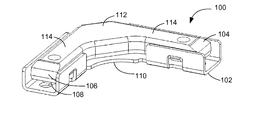
- FIG. 1 is a top perspective view of an example suspension and tolerance absorption subassembly for a display screen
- FIG. 2 is an exploded view of the example suspension and tolerance absorption subassembly illustrated in FIG. 1 ;
- FIG. 3 is a cross-sectional fragmentary view of the example suspension and tolerance absorption subassembly illustrated in FIG. 1 ;
- FIG. 4 is a bottom perspective view of the example suspension and tolerance absorption subassembly illustrated in FIG. 1 ;
- FIG. 5-1 is a perspective view of four example suspension and tolerance absorption subassemblies mounted to a printed circuit board;
- FIG. 5-2 is a fragmentary perspective view of a display screen supported on a printed circuit board by one of the example suspension and tolerance absorption subassemblies illustrated in FIG. 1 ;
- FIG. 6 is a cutaway perspective view of a display screen supported on a printed circuit board within an example electronic device by one of the example suspension and tolerance absorption subassemblies illustrated in FIG. 1 ;
- FIG. 7 is a block diagram of an example mobile communications device.
- a display screen of an electronic device may be supported by one or more subassemblies positioned between the display screen and a printed circuit board (PCB) or any mechanical support structure to which the display screen may be physically secured and electrically connected.
- PCB printed circuit board
- Each subassembly is able to act as an independent suspension for the display screen and is able to cushion the display screen by absorbing mechanical tolerances and mechanical shock and vibration.
- These subassemblies may be used, for example, for suspension of a display screen of a mobile communications device, a laptop computer, a tablet computer, or any other electronic device having a display screen.
- FIG. 1 illustrates a top perspective view of an example suspension and tolerance absorption subassembly for a display screen, hereinafter subassembly 100 .
- Subassembly 100 comprises a first member 102 and a second member 104 , the second member 104 having an outer portion 106 and a flexible inner portion 108 .
- Inner portion 108 is “inner” in the sense that it is interposed between first member 102 and outer portion 106 of second member 104 (and consequently in the assembled subassembly 100 may be less easily visible than first member 102 and outer portion 106 of second member 104 ).
- first member 102 An outer surface 110 of first member 102 is to be proximate to (typically in physical contact with, and in an illustrative implementation, affixed to) a PCB (not shown in FIG. 1 ), while an outer surface 112 of second member 104 is to be proximate to (typically in physical contact with) a rear surface of a display screen (not shown in FIG. 1 ).
- the PCB in addition to other functions) serves as a framework to which various components, such as the display screen, are secured.
- first member 102 may be considered to be an example of a first substantially rigid support means
- outer portion 106 of second member 104 may be considered to be an example of a second substantially rigid support means
- inner portion 108 of second member 104 may be considered to be an example of a flexible (or resilient) cushioning means.
- Suspension and tolerance absorption subassembly 100 is illustrated herein as having an L-shaped configuration with two arms 114 .
- alternative configurations are contemplated, including, but not limited to, an I-shaped configuration and a square-shaped configuration.
- Overall dimensions may vary, but for a typical L-shaped configuration, each arm may be about seven millimeters long and about two millimeters wide, and the assembled subassembly may be about one and a quarter millimeters thick.
- FIG. 2 illustrates an exploded perspective view of the example suspension and tolerance absorption subassembly illustrated in FIG. 1 .
- first member 102 is shown apart from second member 104
- second member 104 is in turn shown with outer portion 106 apart from flexible inner portion 108 .
- Outer surface 110 of first member 102 of subassembly may be affixed to a PCB.
- first member 102 of subassembly may be affixed to the PCB by soldering, and first member 102 may be composed of any metal to which solder may be bonded.
- metals include ferrous and non-ferrous metals, such as cold-rolled steel, stainless steel, tin-plated stock, or other coil stock.
- first member 102 is formed from cold-rolled steel #1008 or #1010 or from #304 stainless steel coil stock.
- First member 102 may be formed into the desired shape using progressive stamping according to traditional methods, for example.
- a material hardness of 1 ⁇ 4,1 ⁇ 2, 3 ⁇ 4, or a full hard material may be used.
- Various other rigid and durable materials, such as plastics, may also be used, and they may be affixed to the PCB by a technique other than soldering (such as by an adhesive, spot welding, a mechanical connector such as a screw, etc.).
- Outer surface 112 of second member 104 may bear against or be held in physical contact with a rear surface of the display screen by an external force. Adhesive, or another instrumentality for holding the components together, is usually not necessary to cause the display screen to bear against outer surface 112 .
- the external force may be applied by, for example, connective elements that mount or otherwise physically secure the display screen to the PCB, as described below.
- Outer portion 106 of second member 104 is composed of a material that is typically hard, rigid and durable. Examples of such materials include polymer plastics such as polycarbonate (PC), acrylonitrile butadiene styrene (ABS), or PC/ABS blends.
- outer portion 106 of second member 104 is formed from Lexan siloxane copolymer resin. Outer portion 106 may be formed into the desired shape by injection molding, for example. Outer portion 106 of second member 104 may also be made of various metals or other hard, rigid or durable materials.
- Inner portion 108 of second member 104 is composed of a flexible or resilient material (typically more flexible than outer portion 106 ), including, for example, silicone rubber.
- inner portion 108 of second member 104 is formed from liquid silicone rubber.
- the silicone rubber may be, for example, in the range of 30-70 durometer, such as 40 durometer.
- Inner portion 108 may be formed into the desired shape by injection molding, for example.
- the materials that make up subassembly 100 may be able to withstand reflow oven temperatures.
- the materials that make up subassembly 100 may be able to withstand up to three passes in a reflow oven, including one pass for the front side of the PCB, one pass for the back side of the PCB and one spare pass.
- the capability of handling reflow oven temperatures is not essential to the concepts described herein, but this capability can make manufacturing more convenient and efficient.
- An inner surface 116 of outer portion 106 may be bonded to an inner surface 118 of inner portion 108 .
- This bond may be a mechanical bond or a chemical bond (with or without adhesive) or both.
- inner portion 108 may be co-molded to outer portion 106 , with a chemical bond being formed at the surface(s) of contact between portions 106 and 108 , preventing their ready separation.
- a silicone inner portion 108 may be particularly suited for co-molding to a plastic outer portion 106 because silicone is able to maintain dimensional stability and temperature stability while still providing the flexibility to absorb mechanical tolerances and shock.
- Outer portion 106 and inner portion 108 of second member 104 may be mechanically bonded to one another in any of many ways.
- outer portion 106 may be injection-molded into a shape comprising one or more recesses (such as apertures, indentations, grooves, notches, etc.), and inner portion 108 may be co-molded to outer portion 106 into a shape comprising one or more mating or complementary protrusions, each one of the one or more protrusions filling or otherwise engaging a corresponding one of the one or more recesses.
- the engagement of the recesses of outer portion 106 with the protrusions of inner portion 108 may provide a mechanical bond between outer portion 106 and inner portion 108 , preventing separation of portions 106 and 108 .
- Other forms of mechanical bonding such as the use of screws or clips or clamps to hold the outer portion 106 and inner portion 108 together, are usually unnecessary.
- outer portion 106 may comprise holes 120
- inner portion 108 may comprise complementary protrusions 122
- Inner portion 108 may also comprise additional protrusions 124 corresponding to recesses (not shown) in outer portion 106 .
- additional and alternative protrusions and recesses may be used to provide mechanical bonding between outer portion 106 and inner portion 108 of second member 104 .
- Holes 120 and any recesses in outer portion 106 may be formed, for example, as a result of the shape of the injection mold cavity used to form the outer portion 106 .
- Protrusions 122 and additional protrusions 124 of inner portion 108 may be formed, for example, as a result of the shape of outer portion 106 , to which inner portion 108 is co-molded.
- Outer portion 106 and inner portion 108 may be formed by the same manufacturer or by different manufacturers.
- outer portion 106 may be formed by a first manufacturer and delivered to a second manufacturer where inner portion 108 is formed.
- inner portion 108 may be formed and engaged to outer portion 106 in a single process.
- inner portion 108 and outer portion 106 may be formed apart, and mated in a separate assembly process.
- a surface 126 of inner portion 108 of second member 104 is to be held proximate to (usually in contact with) an inner surface 128 of first member 102 .
- the assembled second member 104 (which includes outer portion 106 and flexible inner portion 108 ) is to be mated to first member 102 .
- Mating may be accomplished in any of several ways, including snap-fitting second member 104 to first member 102 .
- first member 102 may comprise one or more channel-shaped portions 128 (which may be formed, as depicted in FIG. 2 , by side structures substantially perpendicular to outer surface 110 of first member 102 ), where each channel-shaped portion 128 is to receive a corresponding portion of second member 104 , in this case, arm 114 .
- Outer portion 106 may comprise one or more projections 130 extending in a direction substantially parallel to inner surface 126 . Projections 130 may be snap-fit into a corresponding opening 132 located in a side of one of channel-shaped portions 128 .
- a snap-fit assembly is one in which components are physically attached or engaged by one or more locking features that deform to enable the attachment or engagement, then “snap” back from the deformation to maintain or lock the attachment or engagement.
- the formation of channel-shaped portions 128 and openings 132 in first member 102 may be done using progressive stamping.
- first member 102 and outer portion 106 of second member 104 may be generally rigid and durable, the constructions of these members may accommodate elastic deformation to enable or facilitate the snap-fitting. Once parts are snap-fit to one another, they are not readily separable from one another.
- First member 102 may be formed before or after second member 104 or simultaneously with second member 104 .
- First member 102 and second member 104 may be formed by the same manufacturer or by different manufacturers.
- one or both of first member 102 and second member 104 may be delivered separately to a manufacturer for construction of subassembly 100 .
- FIG. 3 illustrates a cross-sectional fragmentary view of example suspension and tolerance absorption subassembly 100 as illustrated in FIG. 1 .
- the subassembly is assembled, with assembled second member 104 (which includes outer portion 106 and flexible inner portion 108 ) mated to first member 102 .
- second member 104 which includes outer portion 106 and flexible inner portion 108
- first member 102 As described with respect to FIG. 2 , in addition to any chemical bond that may be formed at the surface(s) of contact between outer portion 106 and inner portion 108 of second member 104 , a mechanical bond may also be formed by the engagement of protrusions 122 of inner portion 108 with holes 120 of outer portion 106 , preventing separation of portions 106 and 108 .
- first member 102 and second member 104 are apparent from a joint 134 formed between each projection 130 of outer portion 106 of second member 104 and each opening 132 of first member 102 .
- Projections 130 may be (for example) hook-shaped so as to prevent ready separation of second member 104 from first member 102 .
- openings 132 may be larger than projections 130 being accommodated in openings 132 .
- the extended size of openings 132 may permit limited movement of second member 104 relative to first member 102 in a direction illustrated by an arrow 136 .
- outer surface 112 of second member 104 may be brought closer to inner surface 128 of first member 102 upon compression of flexible inner portion 108 .
- Motion in the direction opposite to arrow 136 may be constrained by joint 134 , and motion orthogonal to arrow 136 may be constrained as well.
- subassembly 100 may reduce or prevent damage to a display screen of an electronic device that might normally result from shock and/or vibration associated with dropping the electronic device.
- Subassembly 100 may also provide cushioning to a display screen with touch-screen functionality, such that subassembly 100 may reduce or prevent damage to the display screen resulting from pressure applied by the user's finger.
- subassembly 100 may reduce stress to the display screen caused by deviations from the nominal dimensions of one or more of components of the electronic device.
- FIG. 4 illustrates a bottom perspective view of the example suspension and tolerance absorption subassembly illustrated in FIG. 1 .
- second member 104 of subassembly 100 is snap-fit into first member 102 by snapping projections 130 of second member 104 into openings 132 of channel-shaped portions 128 of first member 102 .
- second member 104 may be snap-fit into first member 102 forming subassembly 100 , and subassembly 100 may be mounted on a PCB using surface mount technology (SMT) component placement systems, also known as pick-and-place robotic machines.
- SMT surface mount technology
- Pick-and-place technology is a cost-effective means of placing surface mount components (SMCs) onto printed circuit boards with a high degree of accuracy. SMCs may be supplied on paper or plastic tape.
- a tape assembly comprises a cavity tape, a cover tape, and one or more SMCs held between the cavity tape and the cover tape.
- Reels of this tape may be loaded onto feeders mounted to the pick-and-place machine. These feeders are known as tape-and-reel feeders.
- the pick-and-place machine normally uses suction nozzles to pick up individual components from tape-and-reel feeders, to rotate the components to the correct orientation and to place them on the appropriate locations on the PCB with high precision.
- the ability to position subassembly 100 on a PCB may be advantageous in the assembly of an electronic device, and the advantages may be terms of efficiency, speed, cost, quality, and shock absorption, for example.
- Multiple subassemblies 100 may be supplied on a tape for mounting on a PCB using pick-and-place technology.
- a tape assembly may comprise one or more subassemblies 100 held between a cavity tape and a cover tape.
- Subassembly 100 may be temporarily secured to the PCB at the desired location by solder paste. Solder paste may have been applied to the PCB earlier. More than one subassembly 100 may be mounted on a PCB for support of a display screen. For example, as illustrated in FIG. 5-1 , four subassemblies 100 may be mounted on a PCB 500 at positions substantially corresponding to four corners of a display screen to be supported by subassemblies 100 . In another example, alternate or additional subassemblies 100 may be mounted on PCB 500 for support of a display screen, for example, at other positions substantially corresponding to the periphery of the display screen or substantially corresponding to the middle of the display screen, or any other positions.
- subassemblies 100 Once subassemblies 100 have been temporarily secured at the desired location, the entire assembly, including the PCB, the temporarily secured subassemblies 100 , and any other surface mount components that have been mounted on or temporarily secured to the PCB, may be subjected to controlled heat to melt the solder paste and permanently connect subassemblies 100 to the PCB. This may be accomplished by passing the entire assembly through a reflow oven.
- subassembly 100 may comprise materials that are able to withstand reflow oven temperatures.
- solder may serve at least two distinct functions: adhering components to one another, and forming one or more electrical connections.
- soldering may serve principally as an adhesive that affixes subassembly 100 to the PCB.
- a display screen may be positioned such that its rear surface (which is opposite the front surface that displays images) is proximate to (and typically in contact with) outer surface 112 of outer portion 106 of second member 104 of each subassembly 100 .
- the display screen may be a liquid crystal display (LCD) screen, an organic electroluminescent (OEL) display screen, an inorganic electroluminescent display screen, or any other display screen.
- one or more subassemblies 100 may be mounted (e.g., by adhesive) to the display screen itself, and may bear against the PCB.
- FIG. 5-2 illustrates a fragmentary perspective view of a display screen 502 being supported by one of subassemblies 100 mounted on PCB 500 .
- Display screen 502 may be secured to PCB 500 using, for example, clips or screws or both or any other fasteners.
- display screen 502 may be screwed down to PCB 500 through a tab 504 .
- Subassembly 100 is interposed between display screen 502 and PCB 500 , and spatially separates display screen 502 from PCB 500 .
- Subassembly 100 may act as a cushion that prevents display screen 502 from being screwed down to a hard stop during mounting of the display screen 502 to the PCB 500 . This may reduce stress on display screen 502 and prevent “hot spots” from forming on display screen 502 .
- FIG. 6 illustrates a cutaway perspective view of display screen 502 being supported by one of subassemblies 100 mounted on PCB 500 within an electronic device 600 .
- FIG. 6 shows the front surface of display screen 502 .
- Electronic device 600 is illustrated as a mobile communications device.
- display screen 502 is screwed down to PCB 500 using one or more screws 604 through one or more corresponding tabs 504 .
- PCB 500 is typically secured within housing 602 , so that housing 602 and PCB 500 remain in a substantially fixed position with respect to one another.
- Housing 602 may be made or formed of any of several materials, typically rigid and durable materials such as plastic or metal.
- FIG. 7 is a simplified block diagram of an example mobile communications device 700 .
- Device 700 is an example of electronic device 600 .
- the components of device 700 are contained within a housing 702 .
- Housing 702 is an example of housing 602 .
- Device 700 comprises a processor 704 coupled to a memory 706 and optionally to one or more other wireless communication interfaces 708 .
- other wireless communication interfaces 708 may comprise a short-range wireless communication interface such as a wireless personal area network interface, possibly compatible with Bluetooth®.
- other wireless communication interfaces 708 may comprise a wireless wide area network (WWAN) interface such as for cellular communications.
- WWAN wireless wide area network
- One or more antennas 710 may be coupled to respective ones of the other wireless communication interfaces 708 .
- An antenna may be shared among more than one wireless communication interface.
- Device 700 also comprises a WLAN interface 712 within a protocol stack 714 that is coupled to processor 704 .
- WLAN interface 712 comprises a WLAN LLC module 716 , a WLAN MAC module 718 and a WLAN PHY module 720 .
- WLAN MAC module 716 may be compatible with one or more standards of the family of IEEE 802.11 wireless communication standards.
- Device 700 also comprises an antenna 722 coupled to WLAN PHY module 720 .
- Protocol stack 714 may comprise higher layers 724 .
- Device 700 is able to communicate with a WLAN access point using WLAN interface 712 .
- Memory 706 may store an operating system 726 to be executed by processor 704 .
- Memory 706 and processor 704 may be mounted to PCB 500 (which is not shown in FIG. 7 ).
- Memory 706 may store applications 728 installed in device 700 to be executed by processor 704 .
- Memory 706 may also store data (not shown) used by operating system 726 and applications 728 .
- Memory 706 may store one or more WLAN connection profiles 730 , each identifying a wireless local area network by its network name.
- Memory 706 may store an audio coder-decoder (codec) 732 or a video codec 734 or both.
- codec audio coder-decoder
- a non-exhaustive list of examples for audio codec 732 includes G.711, G.722, G.723, G.726, G.729, MP3, Windows® Media Audio (WMA), Vector Sum Excited Linear Prediction (VSELP), Digital Speech Standard (DSS), and any other suitable audio codec.
- a non-exhaustive list of examples for video codec 734 includes H.261, H.263, H.264, flavors of Moving Picture Experts Group (MPEG), RealVideo®, Windows® Media Video, DivX®, Pixlet®, and any other suitable video codec.
- MPEG Moving Picture Experts Group
- Device 700 may comprise an audio input element 736 and an audio output element 738 , both coupled to processor 704 .
- Device 700 may comprise a video input element 740 and a video output element 742 , both coupled to processor 704 .
- applications 728 may comprise a VoIP application that works together with audio input element 736 , audio output element 738 , and audio codec 732 .
- applications 728 may comprise a videoconferencing application that works together with audio input element 736 , audio output element 738 , audio codec 732 , video input element 740 , video output element 742 , and video codec 734 .
- Device 700 may optionally comprise a Global Positioning System (GPS) module 744 coupled to processor 704 .
- GPS Global Positioning System
- Device 700 may comprise one or more user input elements 746 coupled to processor 704 .
- user input elements include a keyboard, a keypad, a touch screen, a joystick, a thumbwheel, a roller, a touchpad, an optical pad, and the like.
- Device 700 comprises a display screen 748 coupled to processor 704 , where display screen 748 is a user output element of device 700 .
- display screen 748 is a touch screen, it functions also as a user input element of device 700 .
- Device 700 may comprise one or more additional user output elements coupled to processor 704 .
- Device 700 may optionally comprise one or more alert components 750 coupled to processor 704 , to be activated in order to alert a user, for example, by sounding a buzzer, playing a ringtone, or vibrating.
- alert components 750 coupled to processor 704 , to be activated in order to alert a user, for example, by sounding a buzzer, playing a ringtone, or vibrating.
- Device 700 comprises a power system 752 , one or more batteries 754 coupled to power system 752 , and a connector 756 coupled to power system 752 .
- Connector 756 is connectible to an external power source (not shown) to provide power for charging a power supply such as batteries 754 or for operating device 700 or for both.
- Power system 752 provides electrical coupling between the external power source and batteries 754 , and provides electrical coupling between batteries 754 and the electrical components of device 700 (e.g. processor 704 , memory 706 , and the like). As part of the electrical coupling between the external power source and batteries 754 , power system 752 may control the charging of batteries 754 with electrical charge drawn from the external power source.
- Display screen 748 bears against and is supported by one or more suspension and tolerance absorption subassemblies 758 positioned between display screen 748 and the PCB to which display screen 748 is secured.
- the double-ended arrow on FIG. 7 between display screen 748 and subassemblies 758 indicates a mechanical, rather than an electronic or signal-based, relationship between display screen 748 and subassemblies 758 .
- Subassemblies 758 are examples of subassembly 100 . Each of subassemblies 758 is able to act as an independent suspension for display screen 748 and is able to cushion display screen 748 by absorbing mechanical tolerances and mechanical shock and vibration.
- display screen 748 (or a portion thereof) has some restricted freedom to move in a direction toward the PCB. Movement toward the PCB is constrained by the cushioning of the subassemblies 758 . In some circumstances (such as when display screen 748 has been pushed toward the PCB), the display screen 748 (or a portion thereof) has some restricted freedom to move in a direction away from the PCB, but this movement may be constrained by subassemblies 758 and the fasteners that secure display screen 748 to the PCB. Movement of display screen 748 in other directions (e.g., in any direction substantially parallel to a plane of the PCB) may likewise be constrained by subassemblies 758 and the fasteners.
- Device 700 may comprise other elements that, for clarity, are not illustrated in FIG. 7 . Similarly, device 700 may comprise a subset of the elements illustrated in FIG. 7 .
- One or more implementations may be used to realize one or more benefits, some of which have been mentioned already.
- Various implementations offer support and shock absorption for a display screen (an element that may be susceptible to damage in an impact), while also constraining the motion of the display screen with respect to the PCB or the housing.
- the shock absorption supplied by the subassemblies may address the stresses or forces or impacts—whether applied intentionally or unintentionally—that a display screen on a portable electronic device foreseeably may encounter.
- the shock absorption may help protect not only the display screen, but also the PCB, from damage.
- various implementations may offer the capability for the display screen to be depressed on its front surface and to return (by the springiness of the cushioning of the subassemblies) to a neutral starting position.
- the subassemblies may supply protection against shocks, and may also supply the resilience to move a displaced display screen back to neutral starting position. Functions such as these can be performed without expenditure of electrical energy.
- Various implementations also support simplicity or efficiency of assembly, in that the subassemblies may have few moving parts and may be assembled using conventional techniques.
- a number of the implementations of the subassemblies may be capable of being affixed to a PCB in a procedure in which other components (such as electronic components) are affixed to the PCB; such techniques for assembly may be especially efficient in circumstances in which the electronic device has extended functionality and may have a substantial number of components affixed to the PCB.
- Many implementations of the subassembly offer a small “footprint,” taking relatively little space on the PCB.
Abstract
Description
Claims (18)
Priority Applications (1)
| Application Number | Priority Date | Filing Date | Title |
|---|---|---|---|
| US13/092,268 US8823898B2 (en) | 2011-04-22 | 2011-04-22 | Suspension and tolerance absorption subassembly for a display screen |
Applications Claiming Priority (1)
| Application Number | Priority Date | Filing Date | Title |
|---|---|---|---|
| US13/092,268 US8823898B2 (en) | 2011-04-22 | 2011-04-22 | Suspension and tolerance absorption subassembly for a display screen |
Publications (2)
| Publication Number | Publication Date |
|---|---|
| US20120268667A1 US20120268667A1 (en) | 2012-10-25 |
| US8823898B2 true US8823898B2 (en) | 2014-09-02 |
Family
ID=47021075
Family Applications (1)
| Application Number | Title | Priority Date | Filing Date |
|---|---|---|---|
| US13/092,268 Active 2033-03-08 US8823898B2 (en) | 2011-04-22 | 2011-04-22 | Suspension and tolerance absorption subassembly for a display screen |
Country Status (1)
| Country | Link |
|---|---|
| US (1) | US8823898B2 (en) |
Families Citing this family (5)
| Publication number | Priority date | Publication date | Assignee | Title |
|---|---|---|---|---|
| US10162442B2 (en) * | 2013-09-27 | 2018-12-25 | Microsoft Technology Licensing, Llc | Compliant support for a display device |
| US20150199072A1 (en) * | 2014-01-10 | 2015-07-16 | Shenzhen Wave Multimedia Co., Ltd | Infra-red touch-detection and touch-recognition device |
| KR20170112618A (en) * | 2016-04-01 | 2017-10-12 | 주식회사 만도 | Shielding structure of electro control unit |
| KR20180065064A (en) * | 2016-12-06 | 2018-06-18 | 삼성디스플레이 주식회사 | Display Device |
| US20220286545A1 (en) * | 2021-03-02 | 2022-09-08 | Apple Inc. | Handheld electronic device |
Citations (19)
| Publication number | Priority date | Publication date | Assignee | Title |
|---|---|---|---|---|
| US2811408A (en) * | 1954-11-19 | 1957-10-29 | Dow Corning | Method of molding plastic articles |
| US4422728A (en) | 1981-01-30 | 1983-12-27 | Sangamo Weston, Inc. | Liquid crystal mounting and connection scheme |
| JPS63313130A (en) | 1987-06-16 | 1988-12-21 | Seiko Epson Corp | Liquid crystal display device |
| US5002368A (en) | 1989-05-31 | 1991-03-26 | Poqet Computer Corporation | Liquid crystal display mounting structure |
| EP0503427A2 (en) | 1991-03-08 | 1992-09-16 | John Fluke Mfg. Co., Inc. | LCD support bracket |
| US5369399A (en) | 1992-05-04 | 1994-11-29 | Motorola, Inc. | Tolerance accumulating circuit supporting mechanical shock isolator |
| EP0642089A1 (en) | 1993-09-01 | 1995-03-08 | NCR International, Inc. | Computer display assembly |
| JPH08160398A (en) | 1994-12-09 | 1996-06-21 | Rohm Co Ltd | Liquid crystal display device |
| US5774199A (en) | 1995-03-31 | 1998-06-30 | Seiko Epson Corporation | Liquid crystal display device |
| US5929950A (en) | 1996-07-25 | 1999-07-27 | Nec Corporation | Liquid crystal display |
| US6034751A (en) | 1996-04-23 | 2000-03-07 | Nec Corporation | Elastically deformed retaining members within retaining structure of LCD panel for electronic equipment |
| US20020003595A1 (en) | 2000-07-06 | 2002-01-10 | Asahi Kogaku Kogyo Kabushiki Kaisha | Backlighted liquid crystal display assembly mounted on circuit substrate |
| US20070268425A1 (en) * | 2006-05-17 | 2007-11-22 | Sang Won Jung | Liquid crystal display module and method for manufacturing the same |
| US20080158473A1 (en) * | 2006-12-29 | 2008-07-03 | Innocom Technology (Shenzhen) Co., Ltd. | Liquid crystal display with slidably assembled frames |
| US20080259239A1 (en) * | 2007-04-20 | 2008-10-23 | Innolux Display Corp. | Liquid crystal display with deformable fixing member and cooperative blocking member |
| EP2194423A1 (en) | 2008-12-04 | 2010-06-09 | Hannspree, Inc. | LCD panel holding device and method thereof |
| US20100188599A1 (en) * | 2008-12-25 | 2010-07-29 | Tsutomu Arihara | Backlight unit and liquid crystal display device having the same |
| US20110080350A1 (en) * | 2009-10-02 | 2011-04-07 | Research In Motion Limited | Method of synchronizing data acquisition and a portable electronic device configured to perform the same |
| US8049836B2 (en) * | 2007-04-25 | 2011-11-01 | Au Optronics Corporation | Display device, a front frame used therein, and a method of manufacture thereof |
-
2011
- 2011-04-22 US US13/092,268 patent/US8823898B2/en active Active
Patent Citations (21)
| Publication number | Priority date | Publication date | Assignee | Title |
|---|---|---|---|---|
| US2811408A (en) * | 1954-11-19 | 1957-10-29 | Dow Corning | Method of molding plastic articles |
| US4422728A (en) | 1981-01-30 | 1983-12-27 | Sangamo Weston, Inc. | Liquid crystal mounting and connection scheme |
| JPS63313130A (en) | 1987-06-16 | 1988-12-21 | Seiko Epson Corp | Liquid crystal display device |
| US5002368A (en) | 1989-05-31 | 1991-03-26 | Poqet Computer Corporation | Liquid crystal display mounting structure |
| US5363227A (en) | 1989-05-31 | 1994-11-08 | Fujitsu Personal Systems, Inc. | Liquid crystal display mounting structure |
| US5486942A (en) | 1989-05-31 | 1996-01-23 | Fujitsu Personal Systems, Inc. | Method of mounting a liquid crystal display employing shock mounts with receiving slots |
| EP0503427A2 (en) | 1991-03-08 | 1992-09-16 | John Fluke Mfg. Co., Inc. | LCD support bracket |
| US5369399A (en) | 1992-05-04 | 1994-11-29 | Motorola, Inc. | Tolerance accumulating circuit supporting mechanical shock isolator |
| EP0642089A1 (en) | 1993-09-01 | 1995-03-08 | NCR International, Inc. | Computer display assembly |
| JPH08160398A (en) | 1994-12-09 | 1996-06-21 | Rohm Co Ltd | Liquid crystal display device |
| US5774199A (en) | 1995-03-31 | 1998-06-30 | Seiko Epson Corporation | Liquid crystal display device |
| US6034751A (en) | 1996-04-23 | 2000-03-07 | Nec Corporation | Elastically deformed retaining members within retaining structure of LCD panel for electronic equipment |
| US5929950A (en) | 1996-07-25 | 1999-07-27 | Nec Corporation | Liquid crystal display |
| US20020003595A1 (en) | 2000-07-06 | 2002-01-10 | Asahi Kogaku Kogyo Kabushiki Kaisha | Backlighted liquid crystal display assembly mounted on circuit substrate |
| US20070268425A1 (en) * | 2006-05-17 | 2007-11-22 | Sang Won Jung | Liquid crystal display module and method for manufacturing the same |
| US20080158473A1 (en) * | 2006-12-29 | 2008-07-03 | Innocom Technology (Shenzhen) Co., Ltd. | Liquid crystal display with slidably assembled frames |
| US20080259239A1 (en) * | 2007-04-20 | 2008-10-23 | Innolux Display Corp. | Liquid crystal display with deformable fixing member and cooperative blocking member |
| US8049836B2 (en) * | 2007-04-25 | 2011-11-01 | Au Optronics Corporation | Display device, a front frame used therein, and a method of manufacture thereof |
| EP2194423A1 (en) | 2008-12-04 | 2010-06-09 | Hannspree, Inc. | LCD panel holding device and method thereof |
| US20100188599A1 (en) * | 2008-12-25 | 2010-07-29 | Tsutomu Arihara | Backlight unit and liquid crystal display device having the same |
| US20110080350A1 (en) * | 2009-10-02 | 2011-04-07 | Research In Motion Limited | Method of synchronizing data acquisition and a portable electronic device configured to perform the same |
Non-Patent Citations (3)
| Title |
|---|
| Bordovsky, Michal, First Office Action for CA2,778,324, Jan. 31, 2014. |
| Knutsson, Frederic, Extended European Search Report for EP 11163568.6, Sep. 20, 2011. |
| Knutsson, Frederic, First Examination Report for EP 11163568.6, Dec. 18, 2013. |
Also Published As
| Publication number | Publication date |
|---|---|
| US20120268667A1 (en) | 2012-10-25 |
Similar Documents
| Publication | Publication Date | Title |
|---|---|---|
| US10819889B2 (en) | Camera device and mobile terminal using same | |
| US8823898B2 (en) | Suspension and tolerance absorption subassembly for a display screen | |
| US20120177237A1 (en) | Audio port configuration for compact electronic devices | |
| WO2012166994A1 (en) | Portable device protector case | |
| EP3484131B1 (en) | Camera device of a mobile terminal | |
| EP3716007B1 (en) | Electronic device and method for protecting screen | |
| US9431926B2 (en) | Vibration generating apparatus and electronic apparatus including the same | |
| US8699211B2 (en) | Peripheral device for portable electronic device | |
| TWI552271B (en) | Method and apparatus for flexible electronic communicating device | |
| EP2570885B1 (en) | Slim-Type Display Module Fixing Apparatus for Portable Terminal | |
| CN110072038B (en) | Camera assembly and electronic equipment | |
| CN107332951B (en) | Mobile terminal | |
| JP5576821B2 (en) | Electronics | |
| US8837167B2 (en) | Electronic device with card holder | |
| US9137478B2 (en) | Television apparatus and electronic device | |
| CN102077574A (en) | Spacer member for camera module and camera module equipped with the same | |
| US20150172796A1 (en) | Case having speaker mesh module and manufacturing method thereof | |
| CN111565273A (en) | Optical anti-shake motor, camera module and electronic equipment thereof | |
| US8145280B2 (en) | Portable electronic device | |
| CA2778324C (en) | Suspension and tolerance absorption subassembly for a display screen | |
| US8901784B2 (en) | Voice coil motor with spacer | |
| CN107959741B (en) | Terminal device | |
| CN209170513U (en) | Joint tool, CCD camera assembly and electronic equipment | |
| CN111431248A (en) | Charging device for electronic equipment | |
| KR101046132B1 (en) | Lens driving device for auto focus |
Legal Events
| Date | Code | Title | Description |
|---|---|---|---|
| AS | Assignment |
Owner name: RESEARCH IN MOTION LIMITED, CANADA Free format text: ASSIGNMENT OF ASSIGNORS INTEREST;ASSIGNORS:PALECZNY, TODD ROBERT;DEHMOUBED, FARZIN;REEL/FRAME:026252/0350 Effective date: 20110510 |
|
| AS | Assignment |
Owner name: BLACKBERRY LIMITED, ONTARIO Free format text: CHANGE OF NAME;ASSIGNOR:RESEARCH IN MOTION LIMITED;REEL/FRAME:033134/0228 Effective date: 20130709 |
|
| STCF | Information on status: patent grant |
Free format text: PATENTED CASE |
|
| MAFP | Maintenance fee payment |
Free format text: PAYMENT OF MAINTENANCE FEE, 4TH YEAR, LARGE ENTITY (ORIGINAL EVENT CODE: M1551) Year of fee payment: 4 |
|
| MAFP | Maintenance fee payment |
Free format text: PAYMENT OF MAINTENANCE FEE, 8TH YEAR, LARGE ENTITY (ORIGINAL EVENT CODE: M1552); ENTITY STATUS OF PATENT OWNER: LARGE ENTITY Year of fee payment: 8 |
|
| AS | Assignment |
Owner name: MALIKIE INNOVATIONS LIMITED, IRELAND Free format text: ASSIGNMENT OF ASSIGNORS INTEREST;ASSIGNOR:BLACKBERRY LIMITED;REEL/FRAME:064104/0103 Effective date: 20230511 |
|
| AS | Assignment |
Owner name: MALIKIE INNOVATIONS LIMITED, IRELAND Free format text: NUNC PRO TUNC ASSIGNMENT;ASSIGNOR:BLACKBERRY LIMITED;REEL/FRAME:064271/0199 Effective date: 20230511 |