US8822882B2 - Scribing sapphire substrates with a solid state UV laser with edge detection - Google Patents
Scribing sapphire substrates with a solid state UV laser with edge detection Download PDFInfo
- Publication number
- US8822882B2 US8822882B2 US11/191,386 US19138605A US8822882B2 US 8822882 B2 US8822882 B2 US 8822882B2 US 19138605 A US19138605 A US 19138605A US 8822882 B2 US8822882 B2 US 8822882B2
- Authority
- US
- United States
- Prior art keywords
- pulses
- sapphire substrate
- laser
- laser energy
- substrate
- Prior art date
- Legal status (The legal status is an assumption and is not a legal conclusion. Google has not performed a legal analysis and makes no representation as to the accuracy of the status listed.)
- Expired - Fee Related, expires
Links
- 239000000758 substrate Substances 0.000 title claims abstract description 100
- 229910052594 sapphire Inorganic materials 0.000 title claims abstract description 89
- 239000010980 sapphire Substances 0.000 title claims abstract description 89
- 239000007787 solid Substances 0.000 title claims abstract description 17
- 238000003708 edge detection Methods 0.000 title description 12
- 238000000034 method Methods 0.000 claims abstract description 45
- 238000002679 ablation Methods 0.000 claims abstract description 10
- 230000003116 impacting effect Effects 0.000 claims abstract description 3
- 238000004519 manufacturing process Methods 0.000 claims description 14
- 230000008878 coupling Effects 0.000 claims description 13
- 238000010168 coupling process Methods 0.000 claims description 13
- 238000005859 coupling reaction Methods 0.000 claims description 13
- 239000002390 adhesive tape Substances 0.000 claims description 8
- 238000010521 absorption reaction Methods 0.000 claims description 6
- 229910017502 Nd:YVO4 Inorganic materials 0.000 claims description 5
- 230000004044 response Effects 0.000 claims description 2
- 230000001939 inductive effect Effects 0.000 claims 2
- 230000008569 process Effects 0.000 abstract description 21
- 238000005520 cutting process Methods 0.000 abstract description 19
- 235000012431 wafers Nutrition 0.000 description 53
- 230000010287 polarization Effects 0.000 description 23
- 238000007514 turning Methods 0.000 description 16
- 239000000463 material Substances 0.000 description 8
- 239000013078 crystal Substances 0.000 description 6
- 229910003460 diamond Inorganic materials 0.000 description 6
- 239000010432 diamond Substances 0.000 description 6
- 239000002609 medium Substances 0.000 description 5
- 230000003287 optical effect Effects 0.000 description 5
- 238000000926 separation method Methods 0.000 description 5
- IJGRMHOSHXDMSA-UHFFFAOYSA-N Atomic nitrogen Chemical compound N#N IJGRMHOSHXDMSA-UHFFFAOYSA-N 0.000 description 4
- 238000010586 diagram Methods 0.000 description 4
- 238000005516 engineering process Methods 0.000 description 4
- 239000007789 gas Substances 0.000 description 4
- 229910052751 metal Inorganic materials 0.000 description 4
- 239000002184 metal Substances 0.000 description 4
- 230000005855 radiation Effects 0.000 description 4
- 229910009372 YVO4 Inorganic materials 0.000 description 3
- 239000000853 adhesive Substances 0.000 description 3
- 230000001070 adhesive effect Effects 0.000 description 3
- 230000008901 benefit Effects 0.000 description 3
- 230000008859 change Effects 0.000 description 3
- 238000003754 machining Methods 0.000 description 3
- 229910002601 GaN Inorganic materials 0.000 description 2
- JMASRVWKEDWRBT-UHFFFAOYSA-N Gallium nitride Chemical compound [Ga]#N JMASRVWKEDWRBT-UHFFFAOYSA-N 0.000 description 2
- 229910001873 dinitrogen Inorganic materials 0.000 description 2
- 238000012986 modification Methods 0.000 description 2
- 230000004048 modification Effects 0.000 description 2
- 238000012544 monitoring process Methods 0.000 description 2
- 239000010409 thin film Substances 0.000 description 2
- 229910052779 Neodymium Inorganic materials 0.000 description 1
- PNEYBMLMFCGWSK-UHFFFAOYSA-N aluminium oxide Inorganic materials [O-2].[O-2].[O-2].[Al+3].[Al+3] PNEYBMLMFCGWSK-UHFFFAOYSA-N 0.000 description 1
- 238000004364 calculation method Methods 0.000 description 1
- 238000004140 cleaning Methods 0.000 description 1
- 239000004020 conductor Substances 0.000 description 1
- 229910052593 corundum Inorganic materials 0.000 description 1
- 238000005336 cracking Methods 0.000 description 1
- 230000001419 dependent effect Effects 0.000 description 1
- 230000002708 enhancing effect Effects 0.000 description 1
- 238000010304 firing Methods 0.000 description 1
- 230000004907 flux Effects 0.000 description 1
- 230000010365 information processing Effects 0.000 description 1
- 230000007246 mechanism Effects 0.000 description 1
- 238000005459 micromachining Methods 0.000 description 1
- 239000012120 mounting media Substances 0.000 description 1
- QEFYFXOXNSNQGX-UHFFFAOYSA-N neodymium atom Chemical compound [Nd] QEFYFXOXNSNQGX-UHFFFAOYSA-N 0.000 description 1
- 229910052757 nitrogen Inorganic materials 0.000 description 1
- 238000012545 processing Methods 0.000 description 1
- 238000002310 reflectometry Methods 0.000 description 1
- 238000012552 review Methods 0.000 description 1
- 239000004065 semiconductor Substances 0.000 description 1
- 238000003860 storage Methods 0.000 description 1
- 230000001629 suppression Effects 0.000 description 1
- 229910001845 yogo sapphire Inorganic materials 0.000 description 1
Images


Classifications
-
- B—PERFORMING OPERATIONS; TRANSPORTING
- B23—MACHINE TOOLS; METAL-WORKING NOT OTHERWISE PROVIDED FOR
- B23K—SOLDERING OR UNSOLDERING; WELDING; CLADDING OR PLATING BY SOLDERING OR WELDING; CUTTING BY APPLYING HEAT LOCALLY, e.g. FLAME CUTTING; WORKING BY LASER BEAM
- B23K26/00—Working by laser beam, e.g. welding, cutting or boring
- B23K26/36—Removing material
- B23K26/40—Removing material taking account of the properties of the material involved
-
- B23K26/063—
-
- B—PERFORMING OPERATIONS; TRANSPORTING
- B23—MACHINE TOOLS; METAL-WORKING NOT OTHERWISE PROVIDED FOR
- B23K—SOLDERING OR UNSOLDERING; WELDING; CLADDING OR PLATING BY SOLDERING OR WELDING; CUTTING BY APPLYING HEAT LOCALLY, e.g. FLAME CUTTING; WORKING BY LASER BEAM
- B23K26/00—Working by laser beam, e.g. welding, cutting or boring
- B23K26/02—Positioning or observing the workpiece, e.g. with respect to the point of impact; Aligning, aiming or focusing the laser beam
- B23K26/03—Observing, e.g. monitoring, the workpiece
- B23K26/032—Observing, e.g. monitoring, the workpiece using optical means
-
- B—PERFORMING OPERATIONS; TRANSPORTING
- B23—MACHINE TOOLS; METAL-WORKING NOT OTHERWISE PROVIDED FOR
- B23K—SOLDERING OR UNSOLDERING; WELDING; CLADDING OR PLATING BY SOLDERING OR WELDING; CUTTING BY APPLYING HEAT LOCALLY, e.g. FLAME CUTTING; WORKING BY LASER BEAM
- B23K26/00—Working by laser beam, e.g. welding, cutting or boring
- B23K26/02—Positioning or observing the workpiece, e.g. with respect to the point of impact; Aligning, aiming or focusing the laser beam
- B23K26/06—Shaping the laser beam, e.g. by masks or multi-focusing
- B23K26/062—Shaping the laser beam, e.g. by masks or multi-focusing by direct control of the laser beam
- B23K26/0622—Shaping the laser beam, e.g. by masks or multi-focusing by direct control of the laser beam by shaping pulses
-
- B—PERFORMING OPERATIONS; TRANSPORTING
- B23—MACHINE TOOLS; METAL-WORKING NOT OTHERWISE PROVIDED FOR
- B23K—SOLDERING OR UNSOLDERING; WELDING; CLADDING OR PLATING BY SOLDERING OR WELDING; CUTTING BY APPLYING HEAT LOCALLY, e.g. FLAME CUTTING; WORKING BY LASER BEAM
- B23K26/00—Working by laser beam, e.g. welding, cutting or boring
- B23K26/02—Positioning or observing the workpiece, e.g. with respect to the point of impact; Aligning, aiming or focusing the laser beam
- B23K26/06—Shaping the laser beam, e.g. by masks or multi-focusing
- B23K26/073—Shaping the laser spot
-
- B—PERFORMING OPERATIONS; TRANSPORTING
- B23—MACHINE TOOLS; METAL-WORKING NOT OTHERWISE PROVIDED FOR
- B23K—SOLDERING OR UNSOLDERING; WELDING; CLADDING OR PLATING BY SOLDERING OR WELDING; CUTTING BY APPLYING HEAT LOCALLY, e.g. FLAME CUTTING; WORKING BY LASER BEAM
- B23K26/00—Working by laser beam, e.g. welding, cutting or boring
- B23K26/36—Removing material
- B23K26/362—Laser etching
- B23K26/364—Laser etching for making a groove or trench, e.g. for scribing a break initiation groove
-
- B23K26/367—
-
- B23K26/4045—
-
- B23K26/4075—
-
- B—PERFORMING OPERATIONS; TRANSPORTING
- B28—WORKING CEMENT, CLAY, OR STONE
- B28D—WORKING STONE OR STONE-LIKE MATERIALS
- B28D5/00—Fine working of gems, jewels, crystals, e.g. of semiconductor material; apparatus or devices therefor
- B28D5/0005—Fine working of gems, jewels, crystals, e.g. of semiconductor material; apparatus or devices therefor by breaking, e.g. dicing
- B28D5/0011—Fine working of gems, jewels, crystals, e.g. of semiconductor material; apparatus or devices therefor by breaking, e.g. dicing with preliminary treatment, e.g. weakening by scoring
-
- B—PERFORMING OPERATIONS; TRANSPORTING
- B23—MACHINE TOOLS; METAL-WORKING NOT OTHERWISE PROVIDED FOR
- B23K—SOLDERING OR UNSOLDERING; WELDING; CLADDING OR PLATING BY SOLDERING OR WELDING; CUTTING BY APPLYING HEAT LOCALLY, e.g. FLAME CUTTING; WORKING BY LASER BEAM
- B23K2101/00—Articles made by soldering, welding or cutting
- B23K2101/36—Electric or electronic devices
- B23K2101/40—Semiconductor devices
-
- B—PERFORMING OPERATIONS; TRANSPORTING
- B23—MACHINE TOOLS; METAL-WORKING NOT OTHERWISE PROVIDED FOR
- B23K—SOLDERING OR UNSOLDERING; WELDING; CLADDING OR PLATING BY SOLDERING OR WELDING; CUTTING BY APPLYING HEAT LOCALLY, e.g. FLAME CUTTING; WORKING BY LASER BEAM
- B23K2103/00—Materials to be soldered, welded or cut
- B23K2103/30—Organic material
- B23K2103/36—Wood or similar materials
-
- B—PERFORMING OPERATIONS; TRANSPORTING
- B23—MACHINE TOOLS; METAL-WORKING NOT OTHERWISE PROVIDED FOR
- B23K—SOLDERING OR UNSOLDERING; WELDING; CLADDING OR PLATING BY SOLDERING OR WELDING; CUTTING BY APPLYING HEAT LOCALLY, e.g. FLAME CUTTING; WORKING BY LASER BEAM
- B23K2103/00—Materials to be soldered, welded or cut
- B23K2103/50—Inorganic material, e.g. metals, not provided for in B23K2103/02 – B23K2103/26
-
- B23K2201/40—
-
- H—ELECTRICITY
- H01—ELECTRIC ELEMENTS
- H01L—SEMICONDUCTOR DEVICES NOT COVERED BY CLASS H10
- H01L21/00—Processes or apparatus adapted for the manufacture or treatment of semiconductor or solid state devices or of parts thereof
- H01L21/70—Manufacture or treatment of devices consisting of a plurality of solid state components formed in or on a common substrate or of parts thereof; Manufacture of integrated circuit devices or of parts thereof
- H01L21/77—Manufacture or treatment of devices consisting of a plurality of solid state components or integrated circuits formed in, or on, a common substrate
- H01L21/78—Manufacture or treatment of devices consisting of a plurality of solid state components or integrated circuits formed in, or on, a common substrate with subsequent division of the substrate into plural individual devices
-
- H—ELECTRICITY
- H01—ELECTRIC ELEMENTS
- H01L—SEMICONDUCTOR DEVICES NOT COVERED BY CLASS H10
- H01L33/00—Semiconductor devices with at least one potential-jump barrier or surface barrier specially adapted for light emission; Processes or apparatus specially adapted for the manufacture or treatment thereof or of parts thereof; Details thereof
- H01L33/005—Processes
- H01L33/0095—Post-treatment of devices, e.g. annealing, recrystallisation or short-circuit elimination
-
- H—ELECTRICITY
- H01—ELECTRIC ELEMENTS
- H01S—DEVICES USING THE PROCESS OF LIGHT AMPLIFICATION BY STIMULATED EMISSION OF RADIATION [LASER] TO AMPLIFY OR GENERATE LIGHT; DEVICES USING STIMULATED EMISSION OF ELECTROMAGNETIC RADIATION IN WAVE RANGES OTHER THAN OPTICAL
- H01S5/00—Semiconductor lasers
- H01S5/02—Structural details or components not essential to laser action
- H01S5/0201—Separation of the wafer into individual elements, e.g. by dicing, cleaving, etching or directly during growth
-
- H—ELECTRICITY
- H01—ELECTRIC ELEMENTS
- H01S—DEVICES USING THE PROCESS OF LIGHT AMPLIFICATION BY STIMULATED EMISSION OF RADIATION [LASER] TO AMPLIFY OR GENERATE LIGHT; DEVICES USING STIMULATED EMISSION OF ELECTROMAGNETIC RADIATION IN WAVE RANGES OTHER THAN OPTICAL
- H01S5/00—Semiconductor lasers
- H01S5/02—Structural details or components not essential to laser action
- H01S5/0206—Substrates, e.g. growth, shape, material, removal or bonding
- H01S5/0213—Sapphire, quartz or diamond based substrates
-
- H—ELECTRICITY
- H01—ELECTRIC ELEMENTS
- H01S—DEVICES USING THE PROCESS OF LIGHT AMPLIFICATION BY STIMULATED EMISSION OF RADIATION [LASER] TO AMPLIFY OR GENERATE LIGHT; DEVICES USING STIMULATED EMISSION OF ELECTROMAGNETIC RADIATION IN WAVE RANGES OTHER THAN OPTICAL
- H01S5/00—Semiconductor lasers
- H01S5/30—Structure or shape of the active region; Materials used for the active region
- H01S5/32—Structure or shape of the active region; Materials used for the active region comprising PN junctions, e.g. hetero- or double- heterostructures
- H01S5/323—Structure or shape of the active region; Materials used for the active region comprising PN junctions, e.g. hetero- or double- heterostructures in AIIIBV compounds, e.g. AlGaAs-laser, InP-based laser
- H01S5/32308—Structure or shape of the active region; Materials used for the active region comprising PN junctions, e.g. hetero- or double- heterostructures in AIIIBV compounds, e.g. AlGaAs-laser, InP-based laser emitting light at a wavelength less than 900 nm
- H01S5/32341—Structure or shape of the active region; Materials used for the active region comprising PN junctions, e.g. hetero- or double- heterostructures in AIIIBV compounds, e.g. AlGaAs-laser, InP-based laser emitting light at a wavelength less than 900 nm blue laser based on GaN or GaP
Definitions
- the present invention relates to systems and processes used in manufacturing integrated device die, such as integrated circuit and laser die, including diode laser die, formed on sapphire substrates. More particularly, the present invention provides for scribing sapphire substrates using solid state UV lasers, and separating the scribed sapphire substrate into die.
- Sapphire Al 2 O 3 is used as a substrate for a variety of devices.
- the sapphire is a hard material that is optically transmissive, electrically nonconducting and a good conductor of heat. It has become the preferred substrate material in manufacturing of laser diodes.
- blue laser diodes and other structures based on gallium nitride GaN and related materials are manufactured on sapphire substrates in large volume.
- One bottleneck in manufacturing of die on sapphire substrates is the separation of the die from the substrate. Because sapphire is very hard, the typical process requires the use of a diamond tipped blade to scribe a pattern in the substrate.
- the sapphire substrate having an array of semiconductor structures such as laser diodes formed thereon is placed on an adhesive known as “blue tape,” or “wafer tape.”
- a diamond blade is used to scribe the substrate. Mechanical stress is used to crack the substrate along scribe lines. The tape carrying the cracked substrate is then stretched to separate the die.
- a robotic pick and place machine is used to remove the individual die, having typical dimensions in a range of 200 to 500 microns on a side, from the tape.
- the diamond blade requires the manufacturer to allocate a relatively wide scribe line, referred to as a “street,” (for example, 40 to 70 microns) on the substrate, reducing the number of die manufacturable on a single substrate.
- the diamond tip blade must be operated relatively slowly, requiring as much as 1 and a half hours for a 2 inch diameter substrate.
- the diamond tips on the blade wear out and must be replaced often, as much as one blade per wafer. Replacement of the blades slows down the process of manufacturing.
- the blades typically have multiple tips, which must be carefully and precisely aligned for proper cutting each time a new tip is brought on line, and each time a new blade is installed.
- the mechanical scribing process causes cracks, which can damage the die and reduce yields. Typical yields for this process have been reported to be about 70%.
- the present invention provides a method and system for manufacturing integrated device die, such as diode laser die, from a sapphire substrate carrying an array of such integrated devices.
- the present invention is suitable for manufacturing blue laser diodes based on gallium nitride structures. According to the present invention, greater density and greater yield are achieved, while also reducing the time required to separate the individual die from the substrate. Furthermore, the present invention is based on compact, low-cost machines, and otherwise reduces the overall manufacturing costs for such integrated device die.
- the present invention provides a process including mounting a sapphire substrate, carrying an array of integrated devices, on a stage such as a movable X-Y stage including a vacuum chuck.
- pulses of laser energy are directed at a surface of the sapphire substrate using a solid state laser.
- the pulses of laser energy have a wavelength below about 560 nanometers, and preferably between about 150 and 560 nanometers.
- energy density, spot size, and pulse duration are established at levels sufficient to induce ablation of sapphire.
- Control of the system causes the pulses to contact the sapphire substrate in a scribe pattern at a rate of motion causing overlap of successive pulses sufficient to cut scribe lines in the sapphire substrate.
- Embodiments of the present invention produce laser pulses having an energy density between about 10 and 100 joules per square centimeter, a pulse duration between about 10 and 30 nanoseconds, and a spot size between about 5 and 25 microns.
- the repetition rate for the pulses is greater than 5 kHz, and preferably ranges from about 10 kHz to 50 kHz or higher.
- the stage is moved at a rate of motion causing overlap of the pulses in the amount of 50 to 99 percent. By controlling the pulse rate, the rate of motion of the stage, and the energy density, the depth of the scribe line can be precisely controlled.
- the scribe lines are cut to a depth of about one-half the thickness, or more, of the sapphire substrate, so that for an 80 micron thick substrate, the scribe line is cut to a depth in the range of about 35 microns to, for example, 60 microns, and more preferably greater than 40 microns.
- the solid state laser comprises a diode pumped, Q-switched, Nd:YVO 4 laser, including harmonic frequency generators such as nonlinear crystals like LBO, so that output of the laser is provided at one of the second, third, fourth and fifth harmonic frequencies of the 1064 nanometer line produced by the neodymium doped, solid state laser.
- the third harmonic frequency of about 355 nanometers is provided.
- the solid state laser comprises a Q-switched, Nd:YAG laser, operating to provide one of the harmonic frequencies as output.
- the method includes detecting edges of the sapphire substrate while directing pulses at the substrate in the scribe pattern. In response to detected edges, the system prevents the pulses of radiation from being directed off of the substrate.
- Embodiments of the present invention direct the pulses of radiation at the backside of the substrate. This prevents damage potentially caused by heat from reaching the active integrated device die structures. Furthermore, it prevents debris from the ablation process from contaminating the integrated devices on the die.
- embodiments of the invention include placing the top surface of the substrate on an adhesive tape prior to scribing, mounting the substrate with the adhesive tape on the stage, moving the substrate under conditions causing ablation of the sapphire in a scribe pattern on the backside of the substrate, and detecting edges of the substrate during the scribing process to prevent the pulses of radiation from impacting the adhesive tape.
- the die defined by a scribe pattern are separated from the sapphire substrate, by mechanically cracking the substrate along the scribe lines, and using a pick and place robot or other technology known in the art.
- the sapphire substrate is placed on an adhesive tape prior to scribing, and after scribing the substrate is rolled or otherwise mechanically manipulated to break the substrate along scribe lines in the scribe pattern.
- the separated die remain adhered to the adhesive tape, until separated using the pick and place robot, or other technology.
- Embodiments of the invention further provide for controlling polarization of the laser pulses with respect to direction of scribe lines in the scribe pattern.
- the polarization is controlled so that the grooves are more uniform for scribe lines parallel to different axes. Uniformity can be improved by random or circular polarization of the pulses in some embodiments. More preferably, polarization of the pulse is controlled so that the polarization is linear and parallel to the scribe line being cut. It is found that the quality of the groove being formed is more V-shaped with parallel polarization, and more U-shaped with polarization that is not aligned. V-shaped grooves are preferred for more uniform and predictable breaking of the substrate during separation of the die.
- Embodiments of the invention provide for control of the polarization using a laser with an adjustable polarizer, such as a half wave plate, in the optical path.
- the invention also provides a system for scribing sapphire which comprises a solid state laser, as described above, a stage adapted to support and move a sapphire substrate, optics directing pulses to impact of sapphire substrate mounted on the stage, an edge detection system which detects edges of substrate mounted on the stage during movement of the stage, and a control system.
- the control system in embodiments of the invention comprises a computer system coupled to the solid state laser, the stage, and the edge detection system.
- the computer is responsive to the edge detection system and parameters set by users to cause the pulses to impact of the sapphire substrate in a scribe pattern at a rate of motion causing overlap of successive pulses sufficient to cut scribe lines in the sapphire substrate.
- Embodiments of the invention also include a debris exhaust system coupled with the stage.
- Embodiments of the invention include a user interface with logic to set up the scribe pattern, and the operational parameters including pulse repetition rate, stage velocity and energy levels to establish scribe depth, scribe speed and other characteristics of the process.
- FIG. 1 is a simplified block diagram of a sapphire scribing system according to the present invention.
- FIG. 2 is a perspective view of a compact, portable sapphire scribing system according to one embodiment of the present invention.
- FIG. 3 is a simplified block diagram including the laser system and optics for the sapphire scribing system of the present invention.
- FIG. 4 is a simplified diagram of components of the edge detection system according to the present invention.
- FIG. 5 illustrates the overlapping of successive pulses during the cutting of a scribe line.
- FIG. 6 is a perspective view of the stage and debris exhaust system of the sapphire scribing system according to the present invention.
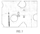
- FIG. 7 illustrates a scribe pattern on a sapphire substrate including an array of integrated laser diodes for cutting into die according to the present invention.
- FIGS. 8A-8C show a relationship between polarization of laser pulses and scribe line scribing direction for uniform V-shaped grooves.
- FIGS. 9-16 are photographs showing experimental results of the scribing process of the present invention.
- FIGS. 9-16 A detailed description of embodiments of the present invention is provided with reference to FIGS. 1 through 8 A- 8 C, and experimental results are shown in FIGS. 9-16 .
- FIG. 1 is a simplified block diagram of a sapphire scribing system according to the present invention.
- a diode pumped, solid state laser 10 generates high-density UV and close-to-UV pulses at a repetition rate in the kHz range.
- the laser comprises a Q-switched Nd:YVO 4 medium delivering third harmonic output as the stream of laser pulses at a repetition rate greater than 10 kHz, with a pulse duration of about 40 nanoseconds.
- the pulses are provided using an optical delivery system 11 and turning mirror 12 to an ultraviolet objective lens 13 , which focuses the pulses on a sapphire substrate 14 .
- the substrate 14 is supported on a vacuum chuck and X/Ystage 15 .
- the wafer is supported face down on an adhesive wafer tape.
- a gas debris removing system 16 cooperates with a gas exhaust system and vacuum 17 to remove debris generated by the ablation of the sapphire substrate.
- a visible light source 18 and a turning mirror 19 deliver white light through the objective lens 13 to the sapphire substrate 14 .
- the edge detection electronics 20 is responsive to light reflected via the objective lens 13 and turning mirror 21 to detect edges of the substrate and prevent pulses of UV radiation from being directed off of the substrate onto the backing wafer tape or elsewhere.
- a camera 22 such as a charge coupled device camera is focused on the wafer 14 and used to generate an image for information processing and monitoring.
- Computer 23 is coupled to the controllable components of the system, and causes the delivery of the pulses, movement of the stage 15 and controls other characteristics of the system to scribe the substrate in a scribe pattern.
- FIG. 2 is a perspective view of a sapphire substrate scribing system in one embodiment of the invention.
- the diode pumped solid state laser is compact and low-cost so that it is efficiently mounted on a cart as illustrated.
- the computer and other system electronics are contained on the cart.
- the computer keyboard 50 is mounted on a keyboard tray, which slides in and out of the cart.
- a flat-panel display 51 is mounted on a swivel base, so that it may be folded in during movement and storage of the cart.
- the system includes a microscope 52 , which enables viewing of the wafer during the cutting process. Images generated by the camera 22 , and graphical user interface tools and other display constructs are presented to the user using the display 51 .
- embodiments of the present invention are provided as a semi-automatic turnkey system using a tabletop laser system and computer mounted on a cart.
- the system provides for manual loading and unloading of wafers.
- the invention contemplates automated wafer loading and unloading systems as well.
- Representative systems are adapted to receive two inch sapphire wafers with die sizes, for example in the range of 250 microns by 250 microns. Smaller and larger die sizes are readily handled.
- the wafer thickness ranges from about 80 to 200 microns, for typical laser diode die, and is mounted face down on a 6.5 inch wafer metal frame using adhesive wafer tape.
- the wafer metal frame is manually placed on the stage and secured using a vacuum chuck. Manual alignment of the wafer is possible using manual stage controls.
- Software controlled scribe patterns are implemented with computer control of the wafer stage, and controllable speed in the X- and Y-directions.
- the system includes a class one laser system which generate spot sizes less than 20 microns in operational conditions.
- a groove is cut, preferably about 40 microns deep, and more preferably greater than about 1 ⁇ 2 thickness of the sapphire substrate.
- Nitrogen gas is used by the debris removing jet, and evacuated using an exhaust pump.
- Throughput of the representative system is about 1 ⁇ 2 hour per wafer, or greater. No damage is caused to the wafer tape because of the edge detection process, supporting greater yield in the die separation process.
- the X/Y stage in one preferred system has a maximum speed of 100 mm per second, and a travel range of greater than 100 mm by 75 mm.
- the resolution of the stage alignment process is about one micron.
- the accuracy over four inches of travel range is less than 4 microns.
- Repeatability of scribe lines provides for deviation of less than three microns.
- the flatness of the stage is less than 1.5 microns deviation per inch. No rotation is required in some embodiments.
- the vacuum chuck is at least 2.5 inches in diameter, on a six inch platform, for holding a two inch wafer during alignment and scribing.
- the laser system in a preferred embodiment is a Q-switched, diode pumped, third harmonic Nd:YVO 4 providing an output at 355 nanometers wavelength.
- the laser provides one watt output power at 20 kHz, and higher, electro-optically Q-switched output using first pulse suppression.
- the pulses have a TEM 00 intensity profile with 10 to 15 micron, or smaller, diameter at 1/e 2 peak magnitude spot size on the target surface.
- the laser pulse duration is about 40 nanoseconds, or less and more preferably between about 30 and 10 nanoseconds, for example about 16 nanoseconds. It is linearly polarized with external rotation control of a half wave plate up to 45 degrees for alignment with the crystalline structure of the sapphire for good and uniform coupling of energy into the sapphire.
- the computer system allows for automated control of the laser and stage movement for defined cutting patterns, which can be set up using the computer.
- a wafer map and cutting definition function allows setup of the scribe pattern including rotation control of the stage.
- Video overlay shows live video of the sample within a software-controlled window to facilitate set up and monitoring of the process.
- Control for the cutting parameters including laser energy, repetition rate and stage speed are provided via the user interface, giving the operator precise control over the depth and quality of the scribing process.
- a pattern alignment function allows the cutting pattern to be moved in the X-, Y- and orthogonal directions to match the actual wafer location during setup.
- FIG. 3 is a basic layout of optical path for one embodiment of the scribing system according to the present invention.
- the optical path includes a laser 50 , optics delivering the output of the laser to a substrate 74 on the vacuum chuck 75 mounted on an X-stage 76 and Y-stage 77 .
- the laser includes a resonant cavity defined by high reflector 51 and output coupler 59 .
- a beam expander 52 , laser medium rod 53 , cylindrical lens 54 , diode array 55 , thin film polarizer 56 , thin film polarizer 57 , and electro-optic Q-switch 58 are included.
- the diode array is operated to pump the rod 53 to induce resonance at the 1064 nm line for Nd:YVO 4 .
- the output beam is directed to turning mirror 60 and turning mirror 61 through spherical focal lens 62 through nonlinear crystal 63 .
- the nonlinear crystal 63 produces a second harmonic and passes the second harmonic along with the primary line through spherical focal lens 64 to a second nonlinear crystal 65 .
- the second nonlinear crystal produces a third harmonic output, among others, which is delivered to turning mirror/filter 66 and turning mirror/filter 67 and half lambda wave plate 68 .
- the wave plate 68 is motorized and acts as a controllable polarizer for the output beam.
- the wave plate 68 is used to align the polarization of the output beam with respect to the scribing direction to make a grooves cut by the laser pulses uniform in the X- and Y-directions.
- the third harmonic output is delivered to optics including turning mirror 69 , beam expander 70 , turning mirror 71 , turning mirror 72 and objective 73 to the sapphire substrate 74 .
- the objective lens 73 is a 20 ⁇ lens in this embodiment.
- Rod 53 in one preferred system is a Nd: YVO 4 solid state laser medium.
- This material allows for shorter pulse durations and higher Q-switch repetition rates than other suitable materials, such as Nd:YAG or Nd:YLF.
- other solid state laser media including without limitation, Nd:YAG, Nd:YLF, and other media suitable for generation of ultraviolet and close-to-ultraviolet pulses at high repetition rates, are utilized in some embodiments.
- Preferred output wavelengths for the solid state Nd-based media includes the second, third, fourth and fifth harmonics of the infrared 1064 nm line, within a range of about 560 nanometers to about 150 nm. Higher wavelengths into the visible range may not be as efficient for ablation of sapphire, while wavelengths below 150 nm require an evacuated optical path for efficient operation.
- FIG. 4 illustrates the edge detection system used in preferred embodiments of the present invention.
- the system includes a white light source 81 which provides light through turning mirror 82 and objective lens 84 to the sapphire substrate 85 on wafer tape 86 , or other mounting media. Reflected light passes through objective lens 84 , turning mirror 83 , turning mirror 82 and is deflected by turning mirror 87 through a spherical focal lens 88 to a photodetector 89 .
- the photodetector 89 is coupled with the computer system, and its output indicates edge detection.
- the edge of the wafer is detected based on the significant difference of light contrast between the wafer surface 85 and the wafer tape 86 or other low reflectivity materials on which the wafer is mounted.
- the computer system stops the motion of the stage upon receipt of the edge detection signal, preventing laser pulses from being directed off the side of the stage.
- FIG. 5 illustrates the overlapping of laser spots according to the present invention.
- pulses emitted by the laser system overlap.
- a first pulse 90 is overlapped by a second pulse 91 which in turn is overlapped by second pulse 92 and so on.
- the amount of overlap determines in part the depth of the scribe lines.
- the overlap can easily be controlled in a range of about 50 to 99 percent.
- FIG. 6 provides a perspective of the stage 100 , objective lens 101 and debris removal jet 102 in one embodiment of the invention.
- the stage 100 includes a vacuum chuck 103 centered on a movable plate 104 .
- a movable plate 104 includes manual adjustment knob 105 for the Y-direction and a similar adjustment knob (not shown) for the X-direction. Also, the movement of the stage is automatically controllable.
- the jet 102 is arranged to deliver air or nitrogen gas into the region of the ablation in order to remove debris.
- a vacuum (not shown) withdraws the gas with the debris from the region of the wafer.
- the repetition rate is controllable within a range of 20 to 50 kHz, with a stage speed ranging up to 8 to 10 mm per second.
- Other combinations of repetition rate and stage speed will be developed according to the needs of a particular implementation.
- FIG. 7 shows a magnified view of an active surface of a sapphire substrate having an array of laser diodes formed thereon.
- Spaces, or streets about 80 microns wide are left between the individual laser diodes to allow room for scribing. However, the white dots should not be cut so the effective street width is less.
- grooves (dark lines within the streets) are machined having a width of 10-15 microns, on the top surface for perspective of the relative widths.
- the backside of the wafer is scribed.
- the streets must be wide enough to accommodate diamond tipped blades. In these prior art systems, such streets have been between at least 40 wide.
- the streets can be reduced to 20 or 30 microns in width or less. This significantly increases the density of devices that can be made on a single substrate and improves throughput in manufacturing process for the die.
- a representative system is based on a Nd: YVO 4 or Nd:YAG laser medium operated at its third harmonic wavelength of 355 nanometers. Theoretically there is very little absorption at this wavelength in a sapphire crystal. However, under a very high intensity flux of laser light, greater than a GigaWatt per cm squared, for example, it is believed that non-linear absorption occurs causing the coupling of the laser energy into the sapphire material. This coupling with sufficient energy density causes ablation of sapphire.
- the laser pulses are highly overlapped during processing as described. The advantages of overlapping the laser pulses during micro-machining include not only improving the smoothness of the machined groove, but also enhancing the laser coupling efficiency into the sapphire material.
- FIGS. 8A-8C illustrate control of linear polarization of the laser pulses with respect to the scribing direction on the sapphire substrate.
- the half wave plate 69 described above with respect to FIG. 3 is used to control polarization of the pulses in order to optimize the coupling of laser energy to the sapphire, and the uniformity of the grooves in the X- and Y-directions.
- FIGS. 8A-8C illustrate control of linear polarization of the laser pulses with respect to the scribing direction on the sapphire substrate.
- the half wave plate 68 described above with respect to FIG. 3 is used to control polarization of the pulses in order to optimize the coupling of laser energy to the sapphire, and the uniformity of the grooves in the X- and Y-directions.
- FIG. 8B illustrates the layout of FIG. 8A , with like components having the same reference numbers.
- half wave plate 203 is rotated 45 degrees relative to the position of FIG. 8A .
- the rotation of the half wave plate 203 causes the polarization of the pulses to rotate 90 degrees as indicated by arrow 208 , extending for this example into the paper.
- the pulses proceed through focus lens 205 maintaining their polarization as indicated by arrow 210 .
- the polarization 210 is aligned with the machining direction of a scribe line 211 parallel with a X-axis.
- FIG. 8C illustrates laser polarization direction relative to the cutting or machining direction of the scribe line.
- a scribe line 215 consists of the sequence of overlapping pulses aligned in a cutting direction 216 .
- the laser polarization direction 217 in the preferred system is parallel with the cutting direction 216 .
- the alignment of polarization parallel with the cutting direction is found to produce uniform V-shaped grooves.
- the V-shaped grooves allow for more uniform separation of the die than can be achieved with grooves that are more U-shaped, or that are less uniform.
- the throughput and the cutting depth of the wafer Two important requirements for the sapphire scribing system are the throughput and the cutting depth of the wafer.
- the cutting depth of sapphire is dependent on the overlap and the energy density. It is required, typically, to cut at least half way through the wafer.
- a 10 kHz repetition rate and maximum energy density 40 j/cm2 are achieved, and used for scribing according to the present invention.
- FIGS. 9-16 are photographs of experimental results of the scribing process using this Nd:YAG embodiment, showing the depth and V-shape of the grooves that can be achieved in representative systems.
- the figures show cross-sections of sample sapphire wafers having thicknesses of about 80 microns, with laser cut grooves more than half the thickness of the wafer.
- an energy density is controlled in a range of about 22.5 to 40.0 j/cm2, and a stage speed in a range of about 2.5 to 5.0 mm/sec.
- the cutting depth is larger than half wafer thickness for the stage speed between 2.5 mm/sec and 5 mm/sec.
- a sapphire scribing system using a Nd: YVO 4 medium operates readily at 20 to 50 kHz, and a maximum energy density can be 45 ⁇ 50 j/cm2.
- the stage speed can be increased to 8 ⁇ 10 mm/sec, for this system.
- computer software is provided to engineers and operators for managing scribing operations as a step in manufacturing of laser diode die.
- the software operates at two levels in this example, designated an engineering interface and an operator interface.
- the engineer has the ability to control the following:
- the present invention provides a process for manufacturing laser diode die, and other integrated device die, formed on sapphire substrates. Procedures according to embodiments of the invention include the following:
- the present invention provides a significantly improved scribing process and system for use with sapphire substrates.
- the process and system are low-cost, high yield, and high throughput compared to prior art sapphire scribing technologies.
Abstract
Description
Laser spot size ˜10 micron, diameter
Stage speed ˜2.5 mm/sec
Then there is a (10 micron/(2.5 mm/sec)=4.0×10−3 sec overlap on a
-
-
FIG. 9 : 22.5 j/cm2/2.5 mm/sec -
FIG. 10 : 30.0 j/cm2/2.5 mm/sec -
FIG. 11 : 40.0 j/cm2/2.5 mm/sec -
FIG. 12 : 40.0 j/cm2/3.0 mm/sec -
FIG. 13 : 40.0 j/cm2/3.5 mm/sec -
FIG. 14 : 40.0 j/cm2/4.0 mm/sec -
FIG. 15 : 40.0 j/cm2/4.5 mm/sec -
FIG. 16 : 40.0 j/cm2/5.0 mm/sec
-
-
- Fire the laser
- Change the rep rate
- Change power (from 0 to 100%)
- Adjust the coax light
- Continuous, burst or single shot firing
- Create reference point (two point for XY, and three points for XYZ)
- Ability to re-coordinate: Save, recreate and move a map on a different wafer to coincide with previously determined reference points.
- Create wafer map: which controls the following
- Manipulate wafer map by changing horizontal and vertical spacing
- Size of the wafer scribe pattern
- Explode scribe pattern to individual lines: Take a wafer and make it into several individual lines
- Translate or rotate patterns
- Laser setting: which controls the following:
- Speed of the stage
- Rep rate
- Polarization
- Laser power (0-100%)
- Number of passes
- a Depth of passes
- Explode lines: which controls the following
- Move each line individually
- Change all setting individually
- Translate or rotate lines individually
- Ability to save and recall
- Stop and begin at the beginning of any line
- Ability to turn ON and OFF the vacuum and nitrogen air
- Calibrate the edge detection
-
- Vacuum control (Load the wafer mechanism)
- Place a new map from the tools library
- Ability to rotate the map
- Run the system
- Abort if needed
-
- 1) laying out and forming laser diodes in an array on an active surface of a sapphire substrate, with individual laser diodes separated by streets having a width less than 40 microns, and preferably around 25 microns or less;
- 2) placing the sapphire wafer with the active surface facing down on wafer tape on a metal frame;
- 2) placing the taped wafer with a metal frame on the vacuum chuck of the wafer stage, and turning on the vacuum to secure the wafer and tape to the stage;
- 3) moving the wafer to a home position by controlling the stage
- 4) automatically, or semi-automatically, aligning the wafer position to coordinates established by the computer setup;
- 5) setting up a scribe pattern based on wafer and die size and layout parameters;
- 6) automatically, or semi-automatically, setting up the lighting levels for edge detection;
- 7) setting up stage speed, laser polarization and laser power for the required cutting depth;
- 8) turning on the debris removing system;
- 9) starting the process of laser scribing based on the scribing pattern on one line parallel to one axis;
- 10) continuing the process on other lines and axes, while controlling polarization, until the wafer is finished;
- 11) causing the stage to return to an exit position, turn off the vacuum, and removing the wafer from the chuck;
- 12) cleaning wafer with high-speed air or other gas jet to remove laser machining induced debris;
- 13) applying mechanical pressure to break the wafer along the scribe lines; and
- 14) stretch the wafer tape for separation and transport using a pick and place system to other mounting apparatus.
Claims (18)
Priority Applications (1)
| Application Number | Priority Date | Filing Date | Title |
|---|---|---|---|
| US11/191,386 US8822882B2 (en) | 2002-06-10 | 2005-07-28 | Scribing sapphire substrates with a solid state UV laser with edge detection |
Applications Claiming Priority (4)
| Application Number | Priority Date | Filing Date | Title |
|---|---|---|---|
| US38738102P | 2002-06-10 | 2002-06-10 | |
| US10/208,484 US6580054B1 (en) | 2002-06-10 | 2002-07-30 | Scribing sapphire substrates with a solid state UV laser |
| US10/384,439 US6960739B2 (en) | 2002-06-10 | 2003-03-06 | Scribing sapphire substrates with a solid state UV laser |
| US11/191,386 US8822882B2 (en) | 2002-06-10 | 2005-07-28 | Scribing sapphire substrates with a solid state UV laser with edge detection |
Related Parent Applications (1)
| Application Number | Title | Priority Date | Filing Date |
|---|---|---|---|
| US10/384,439 Division US6960739B2 (en) | 2002-06-10 | 2003-03-06 | Scribing sapphire substrates with a solid state UV laser |
Publications (2)
| Publication Number | Publication Date |
|---|---|
| US20050279740A1 US20050279740A1 (en) | 2005-12-22 |
| US8822882B2 true US8822882B2 (en) | 2014-09-02 |
Family
ID=26903235
Family Applications (6)
| Application Number | Title | Priority Date | Filing Date |
|---|---|---|---|
| US10/208,484 Expired - Lifetime US6580054B1 (en) | 2002-06-10 | 2002-07-30 | Scribing sapphire substrates with a solid state UV laser |
| US10/364,587 Abandoned US20030226830A1 (en) | 2002-06-10 | 2003-02-11 | Scribing sapphire substrates with a solid state UV laser |
| US10/384,439 Expired - Lifetime US6960739B2 (en) | 2002-06-10 | 2003-03-06 | Scribing sapphire substrates with a solid state UV laser |
| US11/117,052 Abandoned US20050215078A1 (en) | 2002-06-10 | 2005-04-28 | Scribing sapphire substrates with a solid state UV laser |
| US11/191,386 Expired - Fee Related US8822882B2 (en) | 2002-06-10 | 2005-07-28 | Scribing sapphire substrates with a solid state UV laser with edge detection |
| US11/748,600 Abandoned US20070248126A1 (en) | 2002-06-10 | 2007-05-15 | Scribing sapphire substrates with a solid state uv laser |
Family Applications Before (4)
| Application Number | Title | Priority Date | Filing Date |
|---|---|---|---|
| US10/208,484 Expired - Lifetime US6580054B1 (en) | 2002-06-10 | 2002-07-30 | Scribing sapphire substrates with a solid state UV laser |
| US10/364,587 Abandoned US20030226830A1 (en) | 2002-06-10 | 2003-02-11 | Scribing sapphire substrates with a solid state UV laser |
| US10/384,439 Expired - Lifetime US6960739B2 (en) | 2002-06-10 | 2003-03-06 | Scribing sapphire substrates with a solid state UV laser |
| US11/117,052 Abandoned US20050215078A1 (en) | 2002-06-10 | 2005-04-28 | Scribing sapphire substrates with a solid state UV laser |
Family Applications After (1)
| Application Number | Title | Priority Date | Filing Date |
|---|---|---|---|
| US11/748,600 Abandoned US20070248126A1 (en) | 2002-06-10 | 2007-05-15 | Scribing sapphire substrates with a solid state uv laser |
Country Status (3)
| Country | Link |
|---|---|
| US (6) | US6580054B1 (en) |
| JP (1) | JP4287641B2 (en) |
| TW (1) | TW568819B (en) |
Cited By (3)
| Publication number | Priority date | Publication date | Assignee | Title |
|---|---|---|---|---|
| US20140091072A1 (en) * | 2010-10-25 | 2014-04-03 | Jot Automation Oy | Circuit board support for laser cutting |
| US20170151632A1 (en) * | 2015-05-12 | 2017-06-01 | Han's Laser Technology Industry Group Co., Ltd. | Laser processing method, apparatus for sapphire and storage medium |
| US10919794B2 (en) | 2017-12-04 | 2021-02-16 | General Atomics | Method of cutting glass using a laser |
Families Citing this family (125)
| Publication number | Priority date | Publication date | Assignee | Title |
|---|---|---|---|---|
| US6676878B2 (en) | 2001-01-31 | 2004-01-13 | Electro Scientific Industries, Inc. | Laser segmented cutting |
| US6587487B2 (en) * | 2000-12-19 | 2003-07-01 | Photonics Industries International, Inc. | Harmonic laser |
| JP2003200279A (en) * | 2001-10-24 | 2003-07-15 | Seiko Epson Corp | Method and apparatus for cutting electrical wiring on substrate, and method and apparatus for manufacturing electronic device |
| US6690692B2 (en) * | 2002-01-29 | 2004-02-10 | Hans Laser Technology Co., Ltd. | Third harmonic laser system |
| US6580054B1 (en) * | 2002-06-10 | 2003-06-17 | New Wave Research | Scribing sapphire substrates with a solid state UV laser |
| US6960813B2 (en) * | 2002-06-10 | 2005-11-01 | New Wave Research | Method and apparatus for cutting devices from substrates |
| US6995032B2 (en) * | 2002-07-19 | 2006-02-07 | Cree, Inc. | Trench cut light emitting diodes and methods of fabricating same |
| JP2004111601A (en) * | 2002-09-18 | 2004-04-08 | Tokyo Seimitsu Co Ltd | Die bonder |
| CA2503854A1 (en) * | 2002-12-20 | 2004-07-15 | Cree, Inc. | Electronic devices including semiconductor mesa structures and conductivity junctions and methods of forming said devices |
| JP2004223542A (en) * | 2003-01-21 | 2004-08-12 | Disco Abrasive Syst Ltd | Laser machining method and laser machining apparatus |
| TWI248244B (en) * | 2003-02-19 | 2006-01-21 | J P Sercel Associates Inc | System and method for cutting using a variable astigmatic focal beam spot |
| WO2004096483A1 (en) * | 2003-04-25 | 2004-11-11 | Nitto Denko Corporation | Method of producing laser-processed product and adhesive sheet, for laser processing used therefor |
| US6949449B2 (en) * | 2003-07-11 | 2005-09-27 | Electro Scientific Industries, Inc. | Method of forming a scribe line on a ceramic substrate |
| US7340087B2 (en) * | 2003-07-14 | 2008-03-04 | Rudolph Technologies, Inc. | Edge inspection |
| JPWO2005025800A1 (en) * | 2003-09-09 | 2006-11-16 | 住友重機械工業株式会社 | Laser processing method and processing apparatus |
| US7085057B2 (en) * | 2003-10-15 | 2006-08-01 | Invenios | Direct-write system and method for roll-to-roll manufacturing of reflective gratings |
| US7008861B2 (en) * | 2003-12-11 | 2006-03-07 | Cree, Inc. | Semiconductor substrate assemblies and methods for preparing and dicing the same |
| EP1714730B1 (en) * | 2003-12-25 | 2012-04-11 | Nitto Denko Corporation | Method of manufacturing by laser workpieces |
| JP4509578B2 (en) | 2004-01-09 | 2010-07-21 | 浜松ホトニクス株式会社 | Laser processing method and laser processing apparatus |
| JP4601965B2 (en) * | 2004-01-09 | 2010-12-22 | 浜松ホトニクス株式会社 | Laser processing method and laser processing apparatus |
| JP4598407B2 (en) * | 2004-01-09 | 2010-12-15 | 浜松ホトニクス株式会社 | Laser processing method and laser processing apparatus |
| EP1721370A2 (en) * | 2004-02-23 | 2006-11-15 | Powerlase Limited | A laser apparatus |
| WO2011123205A1 (en) | 2010-03-30 | 2011-10-06 | Imra America, Inc. | Laser-based material processing apparatus and methods |
| US20050244600A1 (en) * | 2004-04-28 | 2005-11-03 | Wycech Joseph S | Method and apparatus for forming a finished article of manufacture and a finished article of manufacture made by a new and novel process |
| JP4740556B2 (en) * | 2004-06-17 | 2011-08-03 | 三星ダイヤモンド工業株式会社 | Line processing method and laser processing apparatus using laser light. |
| JP2006007250A (en) * | 2004-06-23 | 2006-01-12 | Disco Abrasive Syst Ltd | Workpiece holding device |
| JP4741822B2 (en) * | 2004-09-02 | 2011-08-10 | ルネサスエレクトロニクス株式会社 | Manufacturing method of semiconductor device |
| JP2006123004A (en) * | 2004-09-29 | 2006-05-18 | Mitsubishi Materials Corp | Laser processing method and laser processing apparatus |
| JP2006134971A (en) * | 2004-11-04 | 2006-05-25 | Disco Abrasive Syst Ltd | Laser processing method of wafer |
| US20060097430A1 (en) * | 2004-11-05 | 2006-05-11 | Li Xiaochun | UV pulsed laser machining apparatus and method |
| KR100628276B1 (en) * | 2004-11-05 | 2006-09-27 | 엘지.필립스 엘시디 주식회사 | scribing equipment and cutting equipment of substrate having the same and method for cutting of substrate using the same |
| JP2006135133A (en) * | 2004-11-08 | 2006-05-25 | Disco Abrasive Syst Ltd | Laser processing method of gallium nitride substrate |
| CN100401537C (en) * | 2004-12-07 | 2008-07-09 | 深圳市方大国科光电技术有限公司 | Laser grinding, capable tech. for GaN base LED chip of reducing GaN layer burn |
| WO2006062017A1 (en) * | 2004-12-08 | 2006-06-15 | Laser Solutions Co., Ltd. | Division starting poin forming method in body to be divided, dividing method for body to be divided, and method of processing work by pulse laser beam |
| JP2006186263A (en) * | 2004-12-28 | 2006-07-13 | Disco Abrasive Syst Ltd | Workpiece holding device |
| JP4873863B2 (en) * | 2005-01-14 | 2012-02-08 | 日東電工株式会社 | Manufacturing method of laser processed product and pressure-sensitive adhesive sheet for laser processing |
| JP4854061B2 (en) | 2005-01-14 | 2012-01-11 | 日東電工株式会社 | Manufacturing method of laser processed product and protective sheet for laser processing |
| US7292616B2 (en) * | 2005-02-09 | 2007-11-06 | Ultratech, Inc. | CO2 laser stabilization systems and methods |
| JP4684687B2 (en) * | 2005-03-11 | 2011-05-18 | 株式会社ディスコ | Wafer laser processing method and processing apparatus |
| JP4648044B2 (en) * | 2005-03-15 | 2011-03-09 | 株式会社ディスコ | Laser processing equipment |
| JP2006319198A (en) * | 2005-05-13 | 2006-11-24 | Disco Abrasive Syst Ltd | Laser machining method for wafer and device thereof |
| US7707741B2 (en) * | 2005-06-06 | 2010-05-04 | Holtec International, Inc. | Method and apparatus for dehydrating high level waste based on dew point temperature measurements |
| DE102005039833A1 (en) * | 2005-08-22 | 2007-03-01 | Rowiak Gmbh | Device and method for material separation with laser pulses |
| JP4993886B2 (en) * | 2005-09-07 | 2012-08-08 | 株式会社ディスコ | Laser processing equipment |
| DE102006042280A1 (en) * | 2005-09-08 | 2007-06-06 | IMRA America, Inc., Ann Arbor | Transparent material scribing comprises using single scan of focused beam of ultrashort laser pulses to simultaneously create surface groove in material and modified region(s) within bulk of material |
| US7458765B2 (en) * | 2005-09-23 | 2008-12-02 | Fraunhofer Usa | Diamond hard coating of ferrous substrates |
| CN1954954A (en) * | 2005-10-27 | 2007-05-02 | 鸿富锦精密工业(深圳)有限公司 | Mould processing device |
| JP2007136477A (en) | 2005-11-16 | 2007-06-07 | Disco Abrasive Syst Ltd | Laser beam machining apparatus |
| US7977601B2 (en) * | 2005-11-28 | 2011-07-12 | Electro Scientific Industries, Inc. | X and Y orthogonal cut direction processing with set beam separation using 45 degree beam split orientation apparatus and method |
| JP2007184426A (en) * | 2006-01-06 | 2007-07-19 | Shinko Electric Ind Co Ltd | Manufacturing method of semiconductor device |
| JP4938339B2 (en) * | 2006-04-04 | 2012-05-23 | 株式会社ディスコ | Laser processing equipment |
| US7834293B2 (en) * | 2006-05-02 | 2010-11-16 | Electro Scientific Industries, Inc. | Method and apparatus for laser processing |
| US20070272666A1 (en) * | 2006-05-25 | 2007-11-29 | O'brien James N | Infrared laser wafer scribing using short pulses |
| US8497449B1 (en) * | 2006-05-26 | 2013-07-30 | Synchron Laser Service Inc. | Micro-machining of ceramics using an ytterbium fiber-laser |
| JP4909657B2 (en) * | 2006-06-30 | 2012-04-04 | 株式会社ディスコ | Processing method of sapphire substrate |
| US7732104B2 (en) * | 2007-01-18 | 2010-06-08 | International Business Machines Corporation | System and method for eliminating the structure and edge roughness produced during laser ablation of a material |
| JP2008200694A (en) * | 2007-02-19 | 2008-09-04 | Disco Abrasive Syst Ltd | Method for machining wafer, and laser beam machining apparatus |
| US7858493B2 (en) * | 2007-02-23 | 2010-12-28 | Finisar Corporation | Cleaving edge-emitting lasers from a wafer cell |
| JP5154838B2 (en) | 2007-05-31 | 2013-02-27 | 株式会社ディスコ | Laser processing equipment |
| US20090045179A1 (en) * | 2007-08-15 | 2009-02-19 | Ellen Marie Kosik Williams | Method and system for cutting solid materials using short pulsed laser |
| JP5826027B2 (en) * | 2008-03-21 | 2015-12-02 | イムラ アメリカ インコーポレイテッド | Laser-based material processing method and system |
| JP2009229266A (en) * | 2008-03-24 | 2009-10-08 | Disco Abrasive Syst Ltd | Work edge detector, and laser machining method and apparatus |
| US8033011B2 (en) * | 2008-08-07 | 2011-10-11 | Win Semiconductors Corp. | Method for mounting a thinned semiconductor wafer on a carrier substrate |
| KR20110105385A (en) * | 2008-12-19 | 2011-09-26 | 어플라이드 머티어리얼스, 인코포레이티드 | Illumination methods and systems for laser scribe detection and alignment in thin film solar cell fabrication |
| JP2010274328A (en) * | 2009-04-30 | 2010-12-09 | Mitsuboshi Diamond Industrial Co Ltd | Laser beam machining method and laser beam machining device |
| US8319146B2 (en) * | 2009-05-05 | 2012-11-27 | General Electric Company | Method and apparatus for laser cutting a trench |
| CN101879657B (en) * | 2009-05-08 | 2016-06-29 | 东莞市中镓半导体科技有限公司 | Solid laser lift equipment and stripping means |
| JP4961468B2 (en) | 2009-10-29 | 2012-06-27 | 三星ダイヤモンド工業株式会社 | Laser processing method, workpiece dividing method, and laser processing apparatus |
| US20130256286A1 (en) * | 2009-12-07 | 2013-10-03 | Ipg Microsystems Llc | Laser processing using an astigmatic elongated beam spot and using ultrashort pulses and/or longer wavelengths |
| JP5587595B2 (en) | 2009-12-11 | 2014-09-10 | 株式会社ディスコ | Laser processing equipment |
| JP5056839B2 (en) | 2009-12-25 | 2012-10-24 | 三星ダイヤモンド工業株式会社 | Workpiece processing method and workpiece division method |
| US8519298B2 (en) * | 2010-03-25 | 2013-08-27 | Veeco Instruments, Inc. | Split laser scribe |
| US8735772B2 (en) | 2011-02-20 | 2014-05-27 | Electro Scientific Industries, Inc. | Method and apparatus for improved laser scribing of opto-electric devices |
| JP5860221B2 (en) * | 2011-03-17 | 2016-02-16 | 株式会社ディスコ | Laser processing method for nonlinear crystal substrate |
| US9174304B2 (en) * | 2011-10-25 | 2015-11-03 | Eisuke Minehara | Laser decontamination device |
| JP6254540B2 (en) * | 2012-03-12 | 2017-12-27 | ロレックス・ソシエテ・アノニムRolex Sa | Clock element engraving method and clock element obtained by the method |
| JP6008565B2 (en) * | 2012-05-02 | 2016-10-19 | 株式会社ディスコ | Processing method of optical device wafer |
| JP6020884B2 (en) * | 2012-05-31 | 2016-11-02 | 住友化学株式会社 | Laser processing method |
| JP5354064B2 (en) * | 2012-06-15 | 2013-11-27 | 三星ダイヤモンド工業株式会社 | Laser processing apparatus, workpiece processing method, and workpiece dividing method |
| JP5965239B2 (en) | 2012-07-31 | 2016-08-03 | 三星ダイヤモンド工業株式会社 | Bonded substrate processing method and processing apparatus |
| US8842358B2 (en) | 2012-08-01 | 2014-09-23 | Gentex Corporation | Apparatus, method, and process with laser induced channel edge |
| TWI543833B (en) * | 2013-01-28 | 2016-08-01 | 先進科技新加坡有限公司 | Method of radiatively grooving a semiconductor substrate |
| USD745208S1 (en) | 2013-02-12 | 2015-12-08 | Neophotonics Corporation | Support for a beam splitter |
| US10286487B2 (en) | 2013-02-28 | 2019-05-14 | Ipg Photonics Corporation | Laser system and method for processing sapphire |
| CN105556684B (en) | 2013-07-22 | 2019-10-18 | 亮锐控股有限公司 | The method for separating the luminaire being formed on substrate wafer |
| FR3012059B1 (en) * | 2013-10-17 | 2016-01-08 | Centre Nat Rech Scient | METHOD AND DEVICE FOR MICRO-MACHINING BY LASER |
| US9844833B2 (en) * | 2014-01-30 | 2017-12-19 | Apple Inc. | System and method for laser cutting sapphire using multiple gas media |
| US10220472B2 (en) * | 2014-01-30 | 2019-03-05 | Lasx Industries, Inc | Modeling of laser output from a pulsed laser to achieve a consistent cutting process |
| US9764427B2 (en) * | 2014-02-28 | 2017-09-19 | Ipg Photonics Corporation | Multi-laser system and method for cutting and post-cut processing hard dielectric materials |
| CN106232283B (en) | 2014-02-28 | 2019-03-29 | Ipg光子公司 | It is processed using the multi-beam laser of different wave length and/or multiple laser beams in pulse duration |
| US10343237B2 (en) | 2014-02-28 | 2019-07-09 | Ipg Photonics Corporation | System and method for laser beveling and/or polishing |
| JP6574207B2 (en) | 2014-05-05 | 2019-09-11 | スリーディー グラス ソリューションズ,インク3D Glass Solutions,Inc | 2D and 3D inductors, antennas, and transformers for manufacturing photoactive substrates |
| CN103949779A (en) * | 2014-05-12 | 2014-07-30 | 深圳晶蓝地光电科技有限公司 | Efficient sapphire sheet cutting technology |
| US10639746B1 (en) | 2014-06-20 | 2020-05-05 | Apple Inc. | Ceramic-based components having laser-etched markings |
| WO2016033477A1 (en) | 2014-08-28 | 2016-03-03 | Ipg Photonics Corporation | Multi-laser system and method for cutting and post-cut processing hard dielectric materials |
| WO2016033494A1 (en) | 2014-08-28 | 2016-03-03 | Ipg Photonics Corporation | System and method for laser beveling and/or polishing |
| US10307867B2 (en) * | 2014-11-05 | 2019-06-04 | Asm Technology Singapore Pte Ltd | Laser fiber array for singulating semiconductor wafers |
| US20160172243A1 (en) * | 2014-12-11 | 2016-06-16 | Nxp B.V. | Wafer material removal |
| US10522707B2 (en) | 2015-01-29 | 2019-12-31 | Solaria Corporation | Tiled solar cell laser process |
| RU2582181C1 (en) * | 2015-02-11 | 2016-04-20 | федеральное государственное автономное образовательное учреждение высшего образования "Южный федеральный университет" (Южный федеральный университет) | Method for laser controlled thermal cleavage of sapphire plates |
| GB201502379D0 (en) * | 2015-02-13 | 2015-04-01 | Rolls Royce Plc | An apparatus and a method of machining a shape through a component |
| US10144107B2 (en) | 2015-09-30 | 2018-12-04 | Apple Inc. | Ultrasonic polishing systems and methods of polishing brittle components for electronic devices |
| CN105382946A (en) * | 2015-12-17 | 2016-03-09 | 哈尔滨新力光电技术有限公司 | Automatic efficient splintering machine and method for sapphire LED bar |
| JP7071609B2 (en) | 2016-02-25 | 2022-05-19 | スリーディー グラス ソリューションズ,インク | Capacitor array for manufacturing 3D capacitors and photoactive substrates |
| US11161773B2 (en) | 2016-04-08 | 2021-11-02 | 3D Glass Solutions, Inc. | Methods of fabricating photosensitive substrates suitable for optical coupler |
| CN109891689B (en) | 2016-12-05 | 2021-05-11 | 极光先进雷射株式会社 | Laser device |
| KR102437366B1 (en) * | 2017-02-09 | 2022-08-29 | 유에스 신써틱 코포레이션 | Energy machined polycrystalline diamond compacts and related methods |
| WO2018200804A1 (en) | 2017-04-28 | 2018-11-01 | 3D Glass Solutions, Inc. | Rf circulator |
| WO2019010045A1 (en) | 2017-07-07 | 2019-01-10 | 3D Glass Solutions, Inc. | 2d and 3d rf lumped element devices for rf system in a package photoactive glass substrates |
| JP2019040919A (en) * | 2017-08-22 | 2019-03-14 | 株式会社ディスコ | Cutting machine and method for detecting groove |
| US10854946B2 (en) | 2017-12-15 | 2020-12-01 | 3D Glass Solutions, Inc. | Coupled transmission line resonate RF filter |
| JP7226832B2 (en) | 2018-01-04 | 2023-02-21 | スリーディー グラス ソリューションズ,インク | Impedance-matching conductive structures for high-efficiency RF circuits |
| WO2019199470A1 (en) | 2018-04-10 | 2019-10-17 | 3D Glass Solutions, Inc. | Rf integrated power condition capacitor |
| US10903545B2 (en) | 2018-05-29 | 2021-01-26 | 3D Glass Solutions, Inc. | Method of making a mechanically stabilized radio frequency transmission line device |
| EP3853944B1 (en) | 2018-09-17 | 2023-08-02 | 3D Glass Solutions, Inc. | High efficiency compact slotted antenna with a ground plane |
| JP7257707B2 (en) | 2018-12-28 | 2023-04-14 | スリーディー グラス ソリューションズ,インク | Annular capacitor RF, microwave and MM wave systems |
| KR102642603B1 (en) | 2018-12-28 | 2024-03-05 | 3디 글래스 솔루션즈 인코포레이티드 | Heterogenous integration for rf, microwave and mm wave systems in photoactive glass substrates |
| AU2020253553A1 (en) | 2019-04-05 | 2021-10-28 | 3D Glass Solutions, Inc. | Glass based empty substrate integrated waveguide devices |
| EP3948954B1 (en) * | 2019-04-18 | 2023-06-14 | 3D Glass Solutions, Inc. | High efficiency die dicing and release |
| RU2731167C1 (en) * | 2019-07-11 | 2020-08-31 | Федеральное государственное автономное научное учреждение Институт сверхвысокочастотной полупроводниковой электроники имени В.Г. Мокерова Российской академии наук (ФГАНУ ИСВЧПЭ РАН) | Method of laser plasma-chemical cutting of plates |
| CN112783264A (en) | 2019-11-11 | 2021-05-11 | 苹果公司 | Biometric key including textured ceramic cover |
| US11113494B2 (en) | 2019-11-11 | 2021-09-07 | Apple Inc. | Biometric key including a textured ceramic cover |
| JP2023516817A (en) | 2020-04-17 | 2023-04-20 | スリーディー グラス ソリューションズ,インク | broadband induction |
| US20240058892A1 (en) * | 2021-03-03 | 2024-02-22 | Meng Keong LIM | An integrated x-ray imaging and laser ablating system for precision micromachining |
| CN113420611B (en) * | 2021-06-01 | 2024-03-29 | 煤炭科学研究总院有限公司 | Roadway surrounding rock safety state detection method and device and electronic equipment |
Citations (99)
| Publication number | Priority date | Publication date | Assignee | Title |
|---|---|---|---|---|
| US3626141A (en) | 1970-04-30 | 1971-12-07 | Quantronix Corp | Laser scribing apparatus |
| US3695497A (en) | 1970-08-26 | 1972-10-03 | Ppg Industries Inc | Method of severing glass |
| US3814895A (en) | 1971-12-27 | 1974-06-04 | Electroglas Inc | Laser scriber control system |
| US3816700A (en) | 1971-10-21 | 1974-06-11 | Union Carbide Corp | Apparatus for facilitating laser scribing |
| US3914548A (en) | 1971-06-30 | 1975-10-21 | Benjamin J Barish | Stylus actuated electrical device and electrical kit including same |
| US3974079A (en) | 1971-05-06 | 1976-08-10 | Bayer Aktiengesellschaft | Production of gamma iron oxide |
| JPS5325996A (en) | 1976-08-24 | 1978-03-10 | Toshiba Corp | Laser working method |
| US4169976A (en) | 1976-02-27 | 1979-10-02 | Valfivre S.P.A. | Process for cutting or shaping of a substrate by laser |
| JPS55151351A (en) | 1979-05-16 | 1980-11-25 | Mitsubishi Electric Corp | Cutting method of semiconductor chip |
| US4237601A (en) | 1978-10-13 | 1980-12-09 | Exxon Research & Engineering Co. | Method of cleaving semiconductor diode laser wafers |
| JPS566451A (en) | 1979-06-27 | 1981-01-23 | Mitsubishi Electric Corp | Deviding method of semiconductor device |
| US4296514A (en) | 1977-05-17 | 1981-10-27 | Jiri Dokoupil | Method for continuous processing of flexible workpieces |
| US4328411A (en) | 1980-04-28 | 1982-05-04 | General Electric Company | Cutting amorphous metal by crystallization with a laser or electron beam |
| JPS5781985A (en) | 1981-09-17 | 1982-05-22 | Toshiba Corp | Laser scribing method |
| US4336439A (en) | 1980-10-02 | 1982-06-22 | Coherent, Inc. | Method and apparatus for laser scribing and cutting |
| JPS5844739A (en) | 1981-09-10 | 1983-03-15 | Toshiba Corp | Scribing method for sapphire substrate |
| JPS5844738A (en) | 1981-09-10 | 1983-03-15 | Toshiba Corp | Scribing method for sapphire substrate |
| JPS5868946A (en) | 1981-10-20 | 1983-04-25 | Toshiba Corp | Laser scribing |
| US4401876A (en) | 1980-05-20 | 1983-08-30 | Martin Cooper | Working gemstones |
| US4416577A (en) | 1980-08-06 | 1983-11-22 | Fujitsu Fanuc Limited | Robot hand of an industrial robot |
| US4543464A (en) | 1982-07-19 | 1985-09-24 | Tokyo Shibaura Denki Kabushiki Kaisha | Apparatus for scribing semiconductor wafer with laser beam |
| US4547651A (en) | 1981-05-28 | 1985-10-15 | Mitsubishi Denki Kabushiki Kaisha | Laser machining apparatus |
| US4562333A (en) | 1984-09-04 | 1985-12-31 | General Electric Company | Stress assisted cutting of high temperature embrittled materials |
| JPS61262479A (en) | 1985-05-15 | 1986-11-20 | Amada Co Ltd | Laser cutting method and its device |
| US4664739A (en) | 1983-12-19 | 1987-05-12 | Stauffer Chemical Company | Removal of semiconductor wafers from dicing film |
| US4769523A (en) | 1985-03-08 | 1988-09-06 | Nippon Kogaku K.K. | Laser processing apparatus |
| JPS6472992A (en) | 1987-09-14 | 1989-03-17 | Sumitomo Electric Industries | Diamond synthesizing installation |
| JPS6475191A (en) | 1987-09-14 | 1989-03-20 | Fuji Electric Co Ltd | Laser beam machine |
| US4906011A (en) | 1987-02-26 | 1990-03-06 | Nikko Rica Corporation | Vacuum chuck |
| US4921564A (en) | 1988-05-23 | 1990-05-01 | Semiconductor Equipment Corp. | Method and apparatus for removing circuit chips from wafer handling tape |
| JPH02251851A (en) | 1989-03-24 | 1990-10-09 | Seiko Instr Inc | Photomask |
| US5057664A (en) | 1989-10-20 | 1991-10-15 | Electro Scientific Industries, Inc. | Method and apparatus for laser processing a target material to provide a uniformly smooth, continuous trim profile |
| USRE33947E (en) | 1986-09-26 | 1992-06-02 | Semiconductor Energy Laboratory Co., Ltd. | Laser scribing method |
| US5138131A (en) | 1990-03-07 | 1992-08-11 | Matsushita Electric Industrial Co., Ltd. | Laser cutting method and apparatus for effecting said method |
| JPH0532428A (en) | 1991-07-30 | 1993-02-09 | Hoya Corp | Method for working glass and its apparatus |
| US5214261A (en) | 1990-09-10 | 1993-05-25 | Rockwell International Corporation | Method and apparatus for dicing semiconductor substrates using an excimer laser beam |
| JPH05325996A (en) | 1992-05-22 | 1993-12-10 | Matsushita Electric Ind Co Ltd | Fuel cell of internally reform type fused carbonate |
| JPH06142968A (en) | 1992-10-30 | 1994-05-24 | Hitachi Constr Mach Co Ltd | Pulse laser beam machine and pulse laser beam machining method |
| US5324012A (en) | 1991-07-16 | 1994-06-28 | Nikon Corporation | Holding apparatus for holding an article such as a semiconductor wafer |
| JPH06302900A (en) | 1993-04-09 | 1994-10-28 | Sumitomo Electric Ind Ltd | Optical system of laser resonator |
| US5362681A (en) * | 1992-07-22 | 1994-11-08 | Anaglog Devices, Inc. | Method for separating circuit dies from a wafer |
| US5387776A (en) | 1993-05-11 | 1995-02-07 | General Electric Company | Method of separation of pieces from super hard material by partial laser cut and pressure cleavage |
| JPH0774131A (en) | 1993-09-02 | 1995-03-17 | Matsushita Electric Ind Co Ltd | Dicing apparatus and method of processing semiconductor chip |
| US5516728A (en) | 1994-03-31 | 1996-05-14 | At&T Corp. | Process for fabircating an integrated circuit |
| US5609148A (en) | 1995-03-31 | 1997-03-11 | Siemens Aktiengesellschaft | Method and apparatus for dicing semiconductor wafers |
| US5611946A (en) | 1994-02-18 | 1997-03-18 | New Wave Research | Multi-wavelength laser system, probe station and laser cutter system using the same |
| US5627109A (en) | 1994-09-16 | 1997-05-06 | Sassa; Michinari | Method of manufacturing a semiconductor device that uses a sapphire substrate |
| US5626777A (en) | 1993-03-02 | 1997-05-06 | Hoechst Ceramtec Ag | Process for producing dividable plates of brittle material with high accuracy and apparatus for receiving and precision-grinding the end faces of a plate |
| US5656186A (en) | 1994-04-08 | 1997-08-12 | The Regents Of The University Of Michigan | Method for controlling configuration of laser induced breakdown and ablation |
| JPH1064854A (en) | 1996-07-18 | 1998-03-06 | Hewlett Packard Co <Hp> | Method for cutting wafer |
| JPH10190117A (en) | 1996-12-26 | 1998-07-21 | Nec Corp | Laser beam machining device |
| US5801356A (en) | 1995-08-16 | 1998-09-01 | Santa Barbara Research Center | Laser scribing on glass using Nd:YAG laser |
| EP0863231A1 (en) | 1997-03-04 | 1998-09-09 | Ngk Insulators, Ltd. | A process for dicing a preform made of an oxide single crystal, and a process for producing functional devices |
| US5809987A (en) | 1996-11-26 | 1998-09-22 | Micron Technology,Inc. | Apparatus for reducing damage to wafer cutting blades during wafer dicing |
| JPH10321908A (en) | 1997-05-19 | 1998-12-04 | Nichia Chem Ind Ltd | Nitride group compound semiconductor element and light-emitting semiconductor element and manufacture thereof |
| US5882463A (en) * | 1995-05-05 | 1999-03-16 | Landis & Gyr Technology Innovation Ag | Method of applying a security element to a substrate |
| JPH1196581A (en) | 1997-09-18 | 1999-04-09 | Ricoh Co Ltd | Objective lens and optical pickup |
| JPH11177137A (en) | 1997-12-16 | 1999-07-02 | Nichia Chem Ind Ltd | Manufacture of nitride semiconductor element |
| JPH11224865A (en) | 1997-12-03 | 1999-08-17 | Ngk Insulators Ltd | Cutting method by laser for oxide single-crystal substrate |
| JPH11224866A (en) | 1997-12-03 | 1999-08-17 | Ngk Insulators Ltd | Laser dividing and cutting method |
| US5961852A (en) | 1997-09-09 | 1999-10-05 | Optical Coating Laboratory, Inc. | Laser scribe and break process |
| JPH11267867A (en) | 1998-03-23 | 1999-10-05 | Seiko Epson Corp | Method and device for laser processing |
| US5987920A (en) | 1996-09-19 | 1999-11-23 | U.S. Philips Corporation | Method of producing a patterned surfacial marking on a transparent body |
| US5994205A (en) | 1997-02-03 | 1999-11-30 | Kabushiki Kaisha Toshiba | Method of separating semiconductor devices |
| JP2000042768A (en) | 1998-07-29 | 2000-02-15 | Nkk Corp | Method and device for detecting end of material to be cut |
| JP2000061677A (en) | 1998-08-26 | 2000-02-29 | Samsung Electronics Co Ltd | Method and device for laser beam cutting |
| US6057525A (en) | 1995-09-05 | 2000-05-02 | United States Enrichment Corporation | Method and apparatus for precision laser micromachining |
| JP2000156358A (en) | 1998-07-29 | 2000-06-06 | Lg Electronics Inc | Method and device for processing transparent medium using laser |
| JP2000196186A (en) | 1998-12-25 | 2000-07-14 | Fuji Electric Co Ltd | Group iii nitride laser diode and its manufacturing method |
| US6107162A (en) | 1995-12-19 | 2000-08-22 | Sony Corporation | Method for manufacture of cleaved light emitting semiconductor device |
| US6121118A (en) | 1998-11-30 | 2000-09-19 | Samsung Electronics Co., Ltd. | Chip separation device and method |
| US6126520A (en) | 1996-10-07 | 2000-10-03 | Raytheon Company | Fixture and methodology for coupling an optical component to a machine |
| US6130403A (en) | 1997-07-30 | 2000-10-10 | Nec Corporation | Laser beam machining apparatus, control method therefor, and recording medium for recording a control program therefor |
| US6182733B1 (en) | 1997-06-18 | 2001-02-06 | Caliper Technologies Corp. | Methods of manufacturing microfabricated substrates |
| JP2001170786A (en) | 1999-12-10 | 2001-06-26 | Hitachi Cable Ltd | Method and device for machining substrate of non- metallic material |
| US6271503B1 (en) | 1999-01-20 | 2001-08-07 | International Business Machines Corporation | Dimensional compensating vacuum fixture |
| JP2001232487A (en) | 1999-11-30 | 2001-08-28 | Canon Inc | Laser beam machining device and method, manufacturing method for ink jet recording head using the device or the method and ink jet recording head manufactured by the manufacturing method |
| EP1137072A2 (en) | 2000-03-22 | 2001-09-26 | Matsushita Electric Industrial Co., Ltd. | Semiconductor device comprising a group III / nitride material and method of fabricating the same |
| JP2001300749A (en) | 2000-04-17 | 2001-10-30 | Fuji Xerox Co Ltd | Method of laser beam machining, method of manufacturing work with laser beam, and method of cleaning |
| JP2002033495A (en) | 2000-07-13 | 2002-01-31 | Mitsubishi Heavy Ind Ltd | Manufacturing method for photovoltaic device |
| US20020031899A1 (en) | 1999-06-08 | 2002-03-14 | Ran Manor | Apparatus and method for singulating semiconductor wafers |
| US20020033558A1 (en) | 2000-09-20 | 2002-03-21 | Fahey Kevin P. | UV laser cutting or shape modification of brittle, high melting temperature target materials such as ceramics or glasses |
| US6365429B1 (en) | 1998-12-30 | 2002-04-02 | Xerox Corporation | Method for nitride based laser diode with growth substrate removed using an intermediate substrate |
| US20020063361A1 (en) | 2000-09-20 | 2002-05-30 | Fahey Kevin P. | Laser processing of alumina or metals on or embedded therein |
| US6413839B1 (en) | 1998-10-23 | 2002-07-02 | Emcore Corporation | Semiconductor device separation using a patterned laser projection |
| US6432788B1 (en) | 1999-07-22 | 2002-08-13 | Implant Sciences Corporation | Method for fabricating an emitter-base junction for a gallium nitride bipolar transistor |
| US6448151B2 (en) | 2000-04-04 | 2002-09-10 | Disco Corporation | Process for producing a large number of semiconductor chips from a semiconductor wafer |
| US20020149136A1 (en) * | 2000-09-20 | 2002-10-17 | Baird Brian W. | Ultraviolet laser ablative patterning of microstructures in semiconductors |
| US6509546B1 (en) | 2000-03-15 | 2003-01-21 | International Business Machines Corporation | Laser excision of laminate chip carriers |
| US6514339B1 (en) | 1999-10-29 | 2003-02-04 | Lg. Philips Co., Ltd. | Laser annealing apparatus |
| US6580054B1 (en) * | 2002-06-10 | 2003-06-17 | New Wave Research | Scribing sapphire substrates with a solid state UV laser |
| US6586707B2 (en) | 2000-10-26 | 2003-07-01 | Xsil Technology Limited | Control of laser machining |
| JP3449201B2 (en) | 1997-11-28 | 2003-09-22 | 日亜化学工業株式会社 | Method for manufacturing nitride semiconductor device |
| US6664498B2 (en) | 2001-12-04 | 2003-12-16 | General Atomics | Method and apparatus for increasing the material removal rate in laser machining |
| US6664503B1 (en) | 1999-09-07 | 2003-12-16 | Asahi Glass Company, Ltd. | Method for manufacturing a magnetic disk |
| US6676878B2 (en) | 2001-01-31 | 2004-01-13 | Electro Scientific Industries, Inc. | Laser segmented cutting |
| EP1422796A2 (en) | 2002-11-21 | 2004-05-26 | New Wave Research | Dual head laser system with intracavity polarization and particle image velocimetry system using the same |
| US6806544B2 (en) | 2002-11-05 | 2004-10-19 | New Wave Research | Method and apparatus for cutting devices from conductive substrates secured during cutting by vacuum pressure |
| JP5325996B2 (en) | 2009-01-16 | 2013-10-23 | テレフオンアクチーボラゲット エル エム エリクソン(パブル) | System and method for recovering from gateway server failures |
Family Cites Families (11)
| Publication number | Priority date | Publication date | Assignee | Title |
|---|---|---|---|---|
| JPS576650A (en) | 1980-06-12 | 1982-01-13 | Kogyo Gijutsuin | Medical calculus crushing apparatus |
| JPH0172992U (en) * | 1987-11-04 | 1989-05-17 | ||
| JPH01174936U (en) * | 1988-05-30 | 1989-12-13 | ||
| JPH09253877A (en) * | 1996-03-25 | 1997-09-30 | Sumitomo Electric Ind Ltd | Excimer laser beam processing method, and processed substrate |
| US6031403A (en) * | 1996-11-13 | 2000-02-29 | International Business Machines Corporation | Pull-up and pull-down circuits |
| JP3436858B2 (en) * | 1997-02-27 | 2003-08-18 | シャープ株式会社 | Manufacturing method of thin film solar cell |
| JP3319585B2 (en) | 1998-06-16 | 2002-09-03 | 日亜化学工業株式会社 | Method for manufacturing nitride semiconductor laser device |
| WO2000075983A1 (en) | 1999-06-08 | 2000-12-14 | Kulicke & Soffa Investments, Inc. | A method for dicing wafers with laser scribing |
| JP2003524190A (en) * | 2000-02-23 | 2003-08-12 | コーニンクレッカ フィリップス エレクトロニクス エヌ ヴィ | Integrated circuit with test interface |
| US6586708B1 (en) * | 2001-09-04 | 2003-07-01 | Cusick, Iii Joseph B. | Water vapor cooled nozzle used in the MIG and TIG arc welding process |
| US7259321B2 (en) * | 2002-01-07 | 2007-08-21 | Bp Corporation North America Inc. | Method of manufacturing thin film photovoltaic modules |
-
2002
- 2002-07-30 US US10/208,484 patent/US6580054B1/en not_active Expired - Lifetime
- 2002-10-25 TW TW091125271A patent/TW568819B/en not_active IP Right Cessation
- 2002-11-25 JP JP2002340354A patent/JP4287641B2/en not_active Expired - Fee Related
-
2003
- 2003-02-11 US US10/364,587 patent/US20030226830A1/en not_active Abandoned
- 2003-03-06 US US10/384,439 patent/US6960739B2/en not_active Expired - Lifetime
-
2005
- 2005-04-28 US US11/117,052 patent/US20050215078A1/en not_active Abandoned
- 2005-07-28 US US11/191,386 patent/US8822882B2/en not_active Expired - Fee Related
-
2007
- 2007-05-15 US US11/748,600 patent/US20070248126A1/en not_active Abandoned
Patent Citations (108)
| Publication number | Priority date | Publication date | Assignee | Title |
|---|---|---|---|---|
| US3626141A (en) | 1970-04-30 | 1971-12-07 | Quantronix Corp | Laser scribing apparatus |
| US3695497A (en) | 1970-08-26 | 1972-10-03 | Ppg Industries Inc | Method of severing glass |
| US3974079A (en) | 1971-05-06 | 1976-08-10 | Bayer Aktiengesellschaft | Production of gamma iron oxide |
| US3914548A (en) | 1971-06-30 | 1975-10-21 | Benjamin J Barish | Stylus actuated electrical device and electrical kit including same |
| US3816700A (en) | 1971-10-21 | 1974-06-11 | Union Carbide Corp | Apparatus for facilitating laser scribing |
| US3814895A (en) | 1971-12-27 | 1974-06-04 | Electroglas Inc | Laser scriber control system |
| US4169976A (en) | 1976-02-27 | 1979-10-02 | Valfivre S.P.A. | Process for cutting or shaping of a substrate by laser |
| JPS5325996A (en) | 1976-08-24 | 1978-03-10 | Toshiba Corp | Laser working method |
| US4296514A (en) | 1977-05-17 | 1981-10-27 | Jiri Dokoupil | Method for continuous processing of flexible workpieces |
| US4237601A (en) | 1978-10-13 | 1980-12-09 | Exxon Research & Engineering Co. | Method of cleaving semiconductor diode laser wafers |
| JPS55151351A (en) | 1979-05-16 | 1980-11-25 | Mitsubishi Electric Corp | Cutting method of semiconductor chip |
| JPS566451A (en) | 1979-06-27 | 1981-01-23 | Mitsubishi Electric Corp | Deviding method of semiconductor device |
| US4328411A (en) | 1980-04-28 | 1982-05-04 | General Electric Company | Cutting amorphous metal by crystallization with a laser or electron beam |
| US4401876A (en) | 1980-05-20 | 1983-08-30 | Martin Cooper | Working gemstones |
| US4416577A (en) | 1980-08-06 | 1983-11-22 | Fujitsu Fanuc Limited | Robot hand of an industrial robot |
| US4336439A (en) | 1980-10-02 | 1982-06-22 | Coherent, Inc. | Method and apparatus for laser scribing and cutting |
| US4547651A (en) | 1981-05-28 | 1985-10-15 | Mitsubishi Denki Kabushiki Kaisha | Laser machining apparatus |
| JPS5844738A (en) | 1981-09-10 | 1983-03-15 | Toshiba Corp | Scribing method for sapphire substrate |
| JPS5844739A (en) | 1981-09-10 | 1983-03-15 | Toshiba Corp | Scribing method for sapphire substrate |
| JPS5781985A (en) | 1981-09-17 | 1982-05-22 | Toshiba Corp | Laser scribing method |
| JPS5868946A (en) | 1981-10-20 | 1983-04-25 | Toshiba Corp | Laser scribing |
| US4543464A (en) | 1982-07-19 | 1985-09-24 | Tokyo Shibaura Denki Kabushiki Kaisha | Apparatus for scribing semiconductor wafer with laser beam |
| US4664739A (en) | 1983-12-19 | 1987-05-12 | Stauffer Chemical Company | Removal of semiconductor wafers from dicing film |
| US4562333A (en) | 1984-09-04 | 1985-12-31 | General Electric Company | Stress assisted cutting of high temperature embrittled materials |
| US4769523A (en) | 1985-03-08 | 1988-09-06 | Nippon Kogaku K.K. | Laser processing apparatus |
| JPS61262479A (en) | 1985-05-15 | 1986-11-20 | Amada Co Ltd | Laser cutting method and its device |
| USRE33947E (en) | 1986-09-26 | 1992-06-02 | Semiconductor Energy Laboratory Co., Ltd. | Laser scribing method |
| US4906011A (en) | 1987-02-26 | 1990-03-06 | Nikko Rica Corporation | Vacuum chuck |
| JPS6475191A (en) | 1987-09-14 | 1989-03-20 | Fuji Electric Co Ltd | Laser beam machine |
| JPS6472992A (en) | 1987-09-14 | 1989-03-17 | Sumitomo Electric Industries | Diamond synthesizing installation |
| US4921564A (en) | 1988-05-23 | 1990-05-01 | Semiconductor Equipment Corp. | Method and apparatus for removing circuit chips from wafer handling tape |
| JPH02251851A (en) | 1989-03-24 | 1990-10-09 | Seiko Instr Inc | Photomask |
| US5057664A (en) | 1989-10-20 | 1991-10-15 | Electro Scientific Industries, Inc. | Method and apparatus for laser processing a target material to provide a uniformly smooth, continuous trim profile |
| US5138131A (en) | 1990-03-07 | 1992-08-11 | Matsushita Electric Industrial Co., Ltd. | Laser cutting method and apparatus for effecting said method |
| US5214261A (en) | 1990-09-10 | 1993-05-25 | Rockwell International Corporation | Method and apparatus for dicing semiconductor substrates using an excimer laser beam |
| US5324012A (en) | 1991-07-16 | 1994-06-28 | Nikon Corporation | Holding apparatus for holding an article such as a semiconductor wafer |
| JPH0532428A (en) | 1991-07-30 | 1993-02-09 | Hoya Corp | Method for working glass and its apparatus |
| JPH05325996A (en) | 1992-05-22 | 1993-12-10 | Matsushita Electric Ind Co Ltd | Fuel cell of internally reform type fused carbonate |
| US5362681A (en) * | 1992-07-22 | 1994-11-08 | Anaglog Devices, Inc. | Method for separating circuit dies from a wafer |
| JPH06142968A (en) | 1992-10-30 | 1994-05-24 | Hitachi Constr Mach Co Ltd | Pulse laser beam machine and pulse laser beam machining method |
| US5626777A (en) | 1993-03-02 | 1997-05-06 | Hoechst Ceramtec Ag | Process for producing dividable plates of brittle material with high accuracy and apparatus for receiving and precision-grinding the end faces of a plate |
| JPH06302900A (en) | 1993-04-09 | 1994-10-28 | Sumitomo Electric Ind Ltd | Optical system of laser resonator |
| US5387776A (en) | 1993-05-11 | 1995-02-07 | General Electric Company | Method of separation of pieces from super hard material by partial laser cut and pressure cleavage |
| JPH0774131A (en) | 1993-09-02 | 1995-03-17 | Matsushita Electric Ind Co Ltd | Dicing apparatus and method of processing semiconductor chip |
| US5703713A (en) | 1994-02-18 | 1997-12-30 | New Wave Research | Multi-wavelength variable attenuator and half wave plate |
| US5811751A (en) | 1994-02-18 | 1998-09-22 | New Wave Research | Multi-wavelength laser system, probe station and laser cutter system using the same |
| US5611946A (en) | 1994-02-18 | 1997-03-18 | New Wave Research | Multi-wavelength laser system, probe station and laser cutter system using the same |
| US5963364A (en) | 1994-02-18 | 1999-10-05 | New Wave Research | Multi-wavelength variable attenuator and half wave plate |
| US5516728A (en) | 1994-03-31 | 1996-05-14 | At&T Corp. | Process for fabircating an integrated circuit |
| US5656186A (en) | 1994-04-08 | 1997-08-12 | The Regents Of The University Of Michigan | Method for controlling configuration of laser induced breakdown and ablation |
| US5627109A (en) | 1994-09-16 | 1997-05-06 | Sassa; Michinari | Method of manufacturing a semiconductor device that uses a sapphire substrate |
| US5609148A (en) | 1995-03-31 | 1997-03-11 | Siemens Aktiengesellschaft | Method and apparatus for dicing semiconductor wafers |
| US5882463A (en) * | 1995-05-05 | 1999-03-16 | Landis & Gyr Technology Innovation Ag | Method of applying a security element to a substrate |
| US5801356A (en) | 1995-08-16 | 1998-09-01 | Santa Barbara Research Center | Laser scribing on glass using Nd:YAG laser |
| US6057525A (en) | 1995-09-05 | 2000-05-02 | United States Enrichment Corporation | Method and apparatus for precision laser micromachining |
| US6107162A (en) | 1995-12-19 | 2000-08-22 | Sony Corporation | Method for manufacture of cleaved light emitting semiconductor device |
| JPH1064854A (en) | 1996-07-18 | 1998-03-06 | Hewlett Packard Co <Hp> | Method for cutting wafer |
| US5987920A (en) | 1996-09-19 | 1999-11-23 | U.S. Philips Corporation | Method of producing a patterned surfacial marking on a transparent body |
| US6126520A (en) | 1996-10-07 | 2000-10-03 | Raytheon Company | Fixture and methodology for coupling an optical component to a machine |
| US5809987A (en) | 1996-11-26 | 1998-09-22 | Micron Technology,Inc. | Apparatus for reducing damage to wafer cutting blades during wafer dicing |
| JPH10190117A (en) | 1996-12-26 | 1998-07-21 | Nec Corp | Laser beam machining device |
| US5994205A (en) | 1997-02-03 | 1999-11-30 | Kabushiki Kaisha Toshiba | Method of separating semiconductor devices |
| JPH10305420A (en) | 1997-03-04 | 1998-11-17 | Ngk Insulators Ltd | Method for fabricating matrix made up of oxide single crystal and method for manufacturing functional device |
| EP0863231A1 (en) | 1997-03-04 | 1998-09-09 | Ngk Insulators, Ltd. | A process for dicing a preform made of an oxide single crystal, and a process for producing functional devices |
| US6257224B1 (en) | 1997-03-04 | 2001-07-10 | Ngk Insulators, Ltd. | Process for working a preform made of an oxide single crystal, and a process for producing functional devices |
| JPH10321908A (en) | 1997-05-19 | 1998-12-04 | Nichia Chem Ind Ltd | Nitride group compound semiconductor element and light-emitting semiconductor element and manufacture thereof |
| US6182733B1 (en) | 1997-06-18 | 2001-02-06 | Caliper Technologies Corp. | Methods of manufacturing microfabricated substrates |
| US6130403A (en) | 1997-07-30 | 2000-10-10 | Nec Corporation | Laser beam machining apparatus, control method therefor, and recording medium for recording a control program therefor |
| US5961852A (en) | 1997-09-09 | 1999-10-05 | Optical Coating Laboratory, Inc. | Laser scribe and break process |
| JPH1196581A (en) | 1997-09-18 | 1999-04-09 | Ricoh Co Ltd | Objective lens and optical pickup |
| JP3449201B2 (en) | 1997-11-28 | 2003-09-22 | 日亜化学工業株式会社 | Method for manufacturing nitride semiconductor device |
| JPH11224865A (en) | 1997-12-03 | 1999-08-17 | Ngk Insulators Ltd | Cutting method by laser for oxide single-crystal substrate |
| JPH11224866A (en) | 1997-12-03 | 1999-08-17 | Ngk Insulators Ltd | Laser dividing and cutting method |
| JPH11177137A (en) | 1997-12-16 | 1999-07-02 | Nichia Chem Ind Ltd | Manufacture of nitride semiconductor element |
| JPH11267867A (en) | 1998-03-23 | 1999-10-05 | Seiko Epson Corp | Method and device for laser processing |
| JP2000156358A (en) | 1998-07-29 | 2000-06-06 | Lg Electronics Inc | Method and device for processing transparent medium using laser |
| US6130401A (en) | 1998-07-29 | 2000-10-10 | Lg Electronics Inc. | Device and method for machining transparent medium by laser |
| JP2000042768A (en) | 1998-07-29 | 2000-02-15 | Nkk Corp | Method and device for detecting end of material to be cut |
| US20020125232A1 (en) | 1998-08-26 | 2002-09-12 | Choo Dae-Ho | Laser cutting apparatus and method |
| US20030209528A1 (en) | 1998-08-26 | 2003-11-13 | Choo Dae-Ho | Laser cutting apparatus and method |
| JP2000061677A (en) | 1998-08-26 | 2000-02-29 | Samsung Electronics Co Ltd | Method and device for laser beam cutting |
| US6413839B1 (en) | 1998-10-23 | 2002-07-02 | Emcore Corporation | Semiconductor device separation using a patterned laser projection |
| US6121118A (en) | 1998-11-30 | 2000-09-19 | Samsung Electronics Co., Ltd. | Chip separation device and method |
| JP2000196186A (en) | 1998-12-25 | 2000-07-14 | Fuji Electric Co Ltd | Group iii nitride laser diode and its manufacturing method |
| US6365429B1 (en) | 1998-12-30 | 2002-04-02 | Xerox Corporation | Method for nitride based laser diode with growth substrate removed using an intermediate substrate |
| US6271503B1 (en) | 1999-01-20 | 2001-08-07 | International Business Machines Corporation | Dimensional compensating vacuum fixture |
| US20020031899A1 (en) | 1999-06-08 | 2002-03-14 | Ran Manor | Apparatus and method for singulating semiconductor wafers |
| US6432788B1 (en) | 1999-07-22 | 2002-08-13 | Implant Sciences Corporation | Method for fabricating an emitter-base junction for a gallium nitride bipolar transistor |
| US6664503B1 (en) | 1999-09-07 | 2003-12-16 | Asahi Glass Company, Ltd. | Method for manufacturing a magnetic disk |
| US6514339B1 (en) | 1999-10-29 | 2003-02-04 | Lg. Philips Co., Ltd. | Laser annealing apparatus |
| JP2001232487A (en) | 1999-11-30 | 2001-08-28 | Canon Inc | Laser beam machining device and method, manufacturing method for ink jet recording head using the device or the method and ink jet recording head manufactured by the manufacturing method |
| JP2001170786A (en) | 1999-12-10 | 2001-06-26 | Hitachi Cable Ltd | Method and device for machining substrate of non- metallic material |
| US6509546B1 (en) | 2000-03-15 | 2003-01-21 | International Business Machines Corporation | Laser excision of laminate chip carriers |
| EP1137072A2 (en) | 2000-03-22 | 2001-09-26 | Matsushita Electric Industrial Co., Ltd. | Semiconductor device comprising a group III / nitride material and method of fabricating the same |
| US6448151B2 (en) | 2000-04-04 | 2002-09-10 | Disco Corporation | Process for producing a large number of semiconductor chips from a semiconductor wafer |
| JP2001300749A (en) | 2000-04-17 | 2001-10-30 | Fuji Xerox Co Ltd | Method of laser beam machining, method of manufacturing work with laser beam, and method of cleaning |
| JP2002033495A (en) | 2000-07-13 | 2002-01-31 | Mitsubishi Heavy Ind Ltd | Manufacturing method for photovoltaic device |
| US20020149136A1 (en) * | 2000-09-20 | 2002-10-17 | Baird Brian W. | Ultraviolet laser ablative patterning of microstructures in semiconductors |
| US20020063361A1 (en) | 2000-09-20 | 2002-05-30 | Fahey Kevin P. | Laser processing of alumina or metals on or embedded therein |
| US20020033558A1 (en) | 2000-09-20 | 2002-03-21 | Fahey Kevin P. | UV laser cutting or shape modification of brittle, high melting temperature target materials such as ceramics or glasses |
| US6586707B2 (en) | 2000-10-26 | 2003-07-01 | Xsil Technology Limited | Control of laser machining |
| US6676878B2 (en) | 2001-01-31 | 2004-01-13 | Electro Scientific Industries, Inc. | Laser segmented cutting |
| US6664498B2 (en) | 2001-12-04 | 2003-12-16 | General Atomics | Method and apparatus for increasing the material removal rate in laser machining |
| US6580054B1 (en) * | 2002-06-10 | 2003-06-17 | New Wave Research | Scribing sapphire substrates with a solid state UV laser |
| US6960739B2 (en) | 2002-06-10 | 2005-11-01 | New Wave Research | Scribing sapphire substrates with a solid state UV laser |
| US6806544B2 (en) | 2002-11-05 | 2004-10-19 | New Wave Research | Method and apparatus for cutting devices from conductive substrates secured during cutting by vacuum pressure |
| EP1422796A2 (en) | 2002-11-21 | 2004-05-26 | New Wave Research | Dual head laser system with intracavity polarization and particle image velocimetry system using the same |
| JP5325996B2 (en) | 2009-01-16 | 2013-10-23 | テレフオンアクチーボラゲット エル エム エリクソン(パブル) | System and method for recovering from gateway server failures |
Non-Patent Citations (18)
| Title |
|---|
| "High-power UV Laser is Effective for Material Processing: No Thermal Distortion, High Precision and High Efficiency," (LD Excitation Solid UV Laser Oscillator of Nippon Quantum Design Co., Ltd.) Electronic Journal Co., Ltd. Nov. 15, 2001, vol. 92, pp. 194-195. |
| Blatter, A., et al., "Lubricated sliding performance of laser-patterned sapphire," WEAR, 232 (1999) 226-230. |
| Chen, Hung-Lung, et al., "Laser Successfully Cuts Sapphire Substrate," Optical Communication 93, 37-40, Dec. 2001 (English translation and the original Chinese included with the parent application). |
| English language translation of Office Action Mailed Dec. 24, 2010 in family member application CN 200610159293.3, 5 pages. |
| Furukawa Electric product brochure, "UV-TAPES for Semiconductor Processing" 8 pages (no date available.). |
| Furukawa Electric, "What is UV-TAPES?" http://www.furukawa.co.jp/uvtape/en/whatis.htm (May 23, 2002) 2 pages. |
| Jersch, J., et al., "Nanostructuring with laser radiation in the near field of a tip from a scanning force microscope," Appl. Phys. A 64, 29-32 (1997). |
| Lee, J.-M. et al., "Scribing and cutting a blue LED wafer using a Q-Switched Nd:YAG laser," Appl. Phys. A 70, 561-564 (2000). |
| Middlebusher, Duane et al.-Decision of Rejection for JP 2002-340354 mailed Feb. 6, 2008. |
| Nakamura, Masahiro, "High-power UV laser is effective for material processing: No thermal strain, high precision and high efficiency," Electronic Journal, Electric Journal Co., Ltd., Nov. 15, 2001, vol. 92, pp. 194-195 (English translation from Japanese). |
| Ostendorf, A., et al., "Material Processing Applications for Diode Pumped Solid State Lasers," Lambda Highlights 57, Lambda Physik Pub. (May 2000), 8 pages. |
| Soilmoisture Equipment Corp., Catalog, available at http://www.soilmoisture.com/ceramics.html (no date available). |
| Soilmoisture, "Porous Ceramics Catalog," available at http://www.soilmoisture.com (no date available). |
| Spectra-Physics Business Units: Products http://www.splasers.com/products/oem-products/fcb-yhp-series.html (Oct. 7, 2002), 2 pages. |
| Spectra-Physics: Products http://www.splasers.com/products/oem-products/navigator1.html (Oct. 7, 2002), 2 pages. |
| Veiko, V.L., et al., "Laser Technology and Micro Electronics," Publishing House of the Bulgarian Academy of Sciences, 1991, 12 pages. (Chinese translation of the original Russian and English translation of the Chinese included in parent application.). |
| Villeneuve, Tim, "Nanosecond pulsed lasers improve micro-machining," DESIGNEWS Semiconductor Manufacturing (Jun. 4, 2001) 33-35. |
| Won, William, "Integration of GaN Thin Films with Dissimilar Substrate Materials by Wafer Bonding and Laser Lift-Off," Ph.D. Dissertation, U.C. Berkeley, Fall 1999, 135 pages. |
Cited By (5)
| Publication number | Priority date | Publication date | Assignee | Title |
|---|---|---|---|---|
| US20140091072A1 (en) * | 2010-10-25 | 2014-04-03 | Jot Automation Oy | Circuit board support for laser cutting |
| US9962790B2 (en) * | 2010-10-25 | 2018-05-08 | Jot Automation Oy | Circuit board support for laser cutting |
| US20170151632A1 (en) * | 2015-05-12 | 2017-06-01 | Han's Laser Technology Industry Group Co., Ltd. | Laser processing method, apparatus for sapphire and storage medium |
| US10625375B2 (en) * | 2015-05-12 | 2020-04-21 | Han's Laser Technology Industry Group Co., Ltd. | Laser processing method, apparatus for sapphire and storage medium |
| US10919794B2 (en) | 2017-12-04 | 2021-02-16 | General Atomics | Method of cutting glass using a laser |
Also Published As
| Publication number | Publication date |
|---|---|
| US20070248126A1 (en) | 2007-10-25 |
| US6960739B2 (en) | 2005-11-01 |
| TW568819B (en) | 2004-01-01 |
| US6580054B1 (en) | 2003-06-17 |
| JP4287641B2 (en) | 2009-07-01 |
| JP2004009139A (en) | 2004-01-15 |
| US20050279740A1 (en) | 2005-12-22 |
| US20050215078A1 (en) | 2005-09-29 |
| US20030226832A1 (en) | 2003-12-11 |
| US20030226830A1 (en) | 2003-12-11 |
Similar Documents
| Publication | Publication Date | Title |
|---|---|---|
| US8822882B2 (en) | Scribing sapphire substrates with a solid state UV laser with edge detection | |
| US7112518B2 (en) | Method and apparatus for cutting devices from substrates | |
| US6806544B2 (en) | Method and apparatus for cutting devices from conductive substrates secured during cutting by vacuum pressure | |
| US7364986B2 (en) | Laser beam processing method and laser beam machine | |
| US7134943B2 (en) | Wafer processing method | |
| JP5089735B2 (en) | Laser processing equipment | |
| TWI284580B (en) | Method and apparatus for cutting devices from substrates | |
| JP4584322B2 (en) | Laser processing method | |
| US20050155954A1 (en) | Semiconductor wafer processing method | |
| JP2009503903A (en) | Fabrication of via holes for monolithic microwave integrated circuits | |
| JP5378314B2 (en) | Laser cutting method | |
| TW201304067A (en) | Wafer dicing using hybrid galvanic laser scribing process with plasma etch | |
| US20050082264A1 (en) | Laser beam machine | |
| CN1978167B (en) | System and method for scribing sapphire substrates with a solid state uv laser | |
| US7332415B2 (en) | Silicon wafer dividing method and apparatus | |
| JP3873098B2 (en) | Laser processing method and apparatus | |
| JP5613809B2 (en) | Laser cutting method and laser processing apparatus | |
| US20060099774A1 (en) | Method of laser processing a gallium nitride substrate | |
| CN116727876A (en) | Frequency-locking single-pulse ultraviolet ultrafast laser wafer full-cutting method and system | |
| CN116727878A (en) | Frequency-locking single-pulse green light ultrafast laser wafer full-cutting method and system | |
| CN116727877A (en) | Frequency-locking single-pulse infrared ultrafast laser wafer full-cutting method and system | |
| CN116551190A (en) | Method and system for thinning ultraviolet ultrafast laser beam wafer approximately perpendicular to wafer surface |
Legal Events
| Date | Code | Title | Description |
|---|---|---|---|
| AS | Assignment |
Owner name: ELECTRO SCIENTIFIC INDUSTRIES, INC., OREGON Free format text: ASSIGNMENT OF ASSIGNORS INTEREST;ASSIGNOR:NEW WAVE RESEARCH, INC.;REEL/FRAME:041845/0887 Effective date: 20170404 |
|
| FEPP | Fee payment procedure |
Free format text: MAINTENANCE FEE REMINDER MAILED (ORIGINAL EVENT CODE: REM.) |
|
| LAPS | Lapse for failure to pay maintenance fees |
Free format text: PATENT EXPIRED FOR FAILURE TO PAY MAINTENANCE FEES (ORIGINAL EVENT CODE: EXP.); ENTITY STATUS OF PATENT OWNER: LARGE ENTITY |
|
| STCH | Information on status: patent discontinuation |
Free format text: PATENT EXPIRED DUE TO NONPAYMENT OF MAINTENANCE FEES UNDER 37 CFR 1.362 |
|
| FP | Lapsed due to failure to pay maintenance fee |
Effective date: 20180902 |