US8802451B2 - Method for manufacturing high density non-volatile magnetic memory - Google Patents
Method for manufacturing high density non-volatile magnetic memory Download PDFInfo
- Publication number
- US8802451B2 US8802451B2 US13/610,587 US201213610587A US8802451B2 US 8802451 B2 US8802451 B2 US 8802451B2 US 201213610587 A US201213610587 A US 201213610587A US 8802451 B2 US8802451 B2 US 8802451B2
- Authority
- US
- United States
- Prior art keywords
- layer
- parallel lines
- mask
- lines
- mtj
- Prior art date
- Legal status (The legal status is an assumption and is not a legal conclusion. Google has not performed a legal analysis and makes no representation as to the accuracy of the status listed.)
- Active, expires
Links
Images


Classifications
-
- B—PERFORMING OPERATIONS; TRANSPORTING
- B82—NANOTECHNOLOGY
- B82Y—SPECIFIC USES OR APPLICATIONS OF NANOSTRUCTURES; MEASUREMENT OR ANALYSIS OF NANOSTRUCTURES; MANUFACTURE OR TREATMENT OF NANOSTRUCTURES
- B82Y10/00—Nanotechnology for information processing, storage or transmission, e.g. quantum computing or single electron logic
-
- B—PERFORMING OPERATIONS; TRANSPORTING
- B82—NANOTECHNOLOGY
- B82Y—SPECIFIC USES OR APPLICATIONS OF NANOSTRUCTURES; MEASUREMENT OR ANALYSIS OF NANOSTRUCTURES; MANUFACTURE OR TREATMENT OF NANOSTRUCTURES
- B82Y25/00—Nanomagnetism, e.g. magnetoimpedance, anisotropic magnetoresistance, giant magnetoresistance or tunneling magnetoresistance
-
- G—PHYSICS
- G11—INFORMATION STORAGE
- G11C—STATIC STORES
- G11C11/00—Digital stores characterised by the use of particular electric or magnetic storage elements; Storage elements therefor
- G11C11/02—Digital stores characterised by the use of particular electric or magnetic storage elements; Storage elements therefor using magnetic elements
- G11C11/16—Digital stores characterised by the use of particular electric or magnetic storage elements; Storage elements therefor using magnetic elements using elements in which the storage effect is based on magnetic spin effect
- G11C11/161—Digital stores characterised by the use of particular electric or magnetic storage elements; Storage elements therefor using magnetic elements using elements in which the storage effect is based on magnetic spin effect details concerning the memory cell structure, e.g. the layers of the ferromagnetic memory cell
-
- H—ELECTRICITY
- H10—SEMICONDUCTOR DEVICES; ELECTRIC SOLID-STATE DEVICES NOT OTHERWISE PROVIDED FOR
- H10N—ELECTRIC SOLID-STATE DEVICES NOT OTHERWISE PROVIDED FOR
- H10N50/00—Galvanomagnetic devices
- H10N50/01—Manufacture or treatment
Definitions
- the present invention relates generally to non-volatile magnetic random access memory and particularly to methods of manufacturing memory cells for non-volatile magnetic random access memory (MRAM).
- MRAM non-volatile magnetic random access memory
- FIGS. 1 and 2 illustrate a selected stage of the prior art fabrication process of a non-volatile MRAM array on a wafer.
- the stack of thin film layers are deposited on a substrate containing CMOS circuitry (not shown) and landing pads for electrical connections to the bottom electrode (BE) for the magnetic tunnel junction (MTJ) elements.
- a typical magnetic tunnel junction (MTJ) cell consists of a bottom electrode (BE) and seed layers, followed by an anti-ferromagnetic pinning layer (AFM).
- the composition of AFM layer is typically alloys of IrMn or PtMn.
- a fixed magnetic layer is deposited on top of the AFM layer.
- the fixed magnetic layer typically has the structure of a synthetic anti-ferromagnetic layer with two ferromagnetic layers made from compounds of Co and Fe, separated by a very thin Ru layer to induce anti-ferromagnetic coupling between the two ferromagnetic sub layers.
- a tunnel barrier is deposited on top of the fixed layer.
- the composition of tunnel barrier layer is preferably MgO.
- the tunnel barrier separated the fixed layer from a free magnetic layer preferably made of magnetic materials of ferromagnetic elements Co, Fe, and Ni. Free layer may also contain up to 20 atomic % of B.
- the AFM layer, fixed magnetic layer, tunnel barrier layer, and free magnetic layer make up the important parts of the MTJ.
- the fixed magnetic layer has a magnetic moment direction pinned into a single direction through exchange coupling to the adjacent AFM layer.
- the magnetic moment direction of the free magnetic layer can be changed between the parallel and anti-parallel direction with respect to the fixed magnetic layer.
- the tunnel barrier layer allows electrons to tunnel between the fixed magnetic layer and the free magnetic layer. When the free magnetic layer's magnetic moment is parallel with the fixed layer's magnetic moment, the resistance to electron flow through tunnel barrier layer is lower; and when the free layer's magnetic moment is anti-parallel with the fixed layer's magnetic moment, the resistance to electron flow through tunnel barrier layer is higher. This difference in resistance is also known as “tunnel magneto-resistance” or TMR.
- a top electrode and dielectric layers are deposited on top of the MTJ/bottom electrode stack.
- the dielectric layer functions as an etch mask during the patterning of the MTJ element and bottom electrode.
- the dielectric etch mask has the shape of a post or pillar.
- the control of the critical dimensions of the post shape is rather limited and hence strongly affects the size control of the final MTJ element.
- a fabrication process involving two photolithography steps and two etch steps have been previously been proposed (U.S. Pat. No. 7,863,060 to Belen, et al. (Jan. 4, 2011)).
- the thickness of the dielectric layer in the prior art limits the resolution of the patterning process and introduces a large topography and gap to be filled prior to any subsequent patterning step.
- the current invention addresses this deficiency by using a very thin dielectric mask, as well as provide methods to reduce the size of the MTJ element and to self-align the bitlines to the MTJ elements.
- Embodiments of the present invention include methods for manufacturing of a magnetic tunnel junction (MTJ) array on a wafer using double patterning to achieve dense arrays of MTJs exceeding the limit set by the minimum feature size (F) in every technology node.
- Two orthogonal line patterning steps achieve an array of MTJs located where the orthogonal lines overlap.
- a self-aligned double patterning method embodiment allows for a half pitch capability for the packing of the MTJs in the array.
- the self-aligned double patterning approach also allows for reducing one dimension of the MTJ to create MTJ with aspect ratio larger than one, while the largest dimension of the MTJ is limited by the feature size F and the size is smaller than a traditionally patterned MTJ with an aspect ratio larger than one, where the smallest dimension of the MTJ is limited by the feature size F. Since program current is proportional to area of barrier layer, it helps to reduce program current without any other layout change.
- a set of mask pads that self-define the location of the MTJ pillars are formed over bulk layers for the MTJ cells including the top electrode.
- the materials and thicknesses of the stack of layers that provide the masking function are selected so that after the initial set of mask pads have been patterned, a sequence of etching steps progressively transfers the mask pad shape through the layers in multiple mask layer and down through all of the MTJ cell layers to the form the complete MTJ pillars.
- the sequence of etching steps can progressively consume the upper layer in the mask pads but the selected sequence of layers provides that underlying layers with different etching resistant properties provide the mask for a particular phase.
- the initial mask pads are used in a sequence of etching steps that each form a subsequent mask pad from the multiple layers of material deposited above the top electrode and ultimately etch down to the substrate to form the MTJ pillars including the top electrode.
- An embodiment of set of layers for the sequence of mask pads includes a first (lower) dielectric layer, a thin metal layer, and a second (upper) dielectric layer.
- a planarizing BARC layer is also deposited above the upper dielectric layer as part of the patterning process.
- the shape and location of the initial mask pads in the first group of embodiments are determined by first etching parallel lines in the upper dielectric layer and then forming pads of dielectric material by etching using a second line mask with parallel lines orthogonal to the first lines.
- the initial mask pads are the upper dielectric material disposed on the metal layer.
- the next etching step uses the initial mask pads as a mask to etch through the metal layer with the result being that a bilayer mask pad has been formed on the lower dielectric layer.
- the following etching step uses the bilayer mask pad to etched down through the lower dielectric layer.
- the upper dielectric pad layer is consumed in the process, so that the mask pads now have the metal layer as the upper layer over the lower dielectric layer.
- the top electrode layer is etched.
- the top metal layer in the pads is preferably a different metal than the top electrode to facilitate selective etching, but the lower dielectric pad layer function as a hard mask. Appropriate etching steps are then used to etch through the MTJ and bottom electrode layers to complete the formation of the MTJ cell pillars. Any remaining lower dielectric mask pad material can be removed by etching, then a conventional process can be employed to form the bitline interconnection for each MTJ cell.
- the shape and size of the mask pads is determined by the overlapping area of two sets of separately patterned sets of mask lines. If each set of mask lines has a width equal to the feature size F then the pads will be have an aspect ratio of one. The theoretical square shape will become rounded by increased etching of the edges.
- either or both sets of mask lines can be formed using the self-aligned double patterning (SDP) method described herein that allows for reduction of the mask line width and pitch to one half F.
- SDP self-aligned double patterning
- the embodiments using the SDP method reduce one or both in-plane dimensions of the MTJ pillar and may provide an important reduction in the current required to switch the free layer state without any other layout change other than the MTJ feature size. Reducing the program current required to switch the free layer state is one of the most serious design issues.
- the self-aligned double patterning (SDP) method is used in various embodiments of the invention.
- the first set of parallel mask lines are formed using the SDP method and the second set of orthogonal mask lines can then be formed as described in the first embodiment.
- the SDP method forms a set sacrificial mask lines using conventional photo lithography, which are limited to feature size F.
- the sacrificial mask lines can be photoresist or material deposited using photoresist masks.
- a layer spacer material which is a selected as a material that can survive etching of the sacrificial mask line material in subsequent processing, is deposited over the sacrificial mask lines and then partially etched to leave only wedge-shaped lines of spacer material at the sides of sacrificial mask lines.
- the sacrificial mask line material is removed to leave two lines of wedge-shaped spacer material for each sacrificial mask line.
- the lines of wedge-shaped spacer material spacer are then used as a mask to etch lines into the underlying layer in the stack of mask layers. In this way the first set of lines are formed with a density that is twice that of the photoresist lines and, therefore, exceed the limit set by the minimum feature size (F) of the photo lithography technology.
- a hard mask layer is deposited on the MTJ/BE stack before the set of three mask layers as described above is deposited.
- the top electrode layer is not included at this stage.
- the first set of mask lines is then formed as described above for the first embodiment and used as a mask to etch matching lines in the first (lower) dielectric layer. In turn these dielectric lines are used to etch matching lines in the hard mask layer.
- the hard mask lines are then used to etch lines in the MTJ/BE stack down to the substrate.
- the MTJ/BE lines with the remaining hard mask layer in this embodiment are first covered with a thin conformal layer of SiN followed by a thicker SiO2 which is planarized.
- the top surfaces of the hard mask on the MTJ/BE lines are then exposed by planarization processes.
- a top electrode layer is then deposited over the wafer.
- the second set of orthogonal lines are then formed by a process that starts by depositing dielectric, metal, and BARC layers.
- a photoresist line mask is patterned and lines are etched from the dielectric layer disposed on the top electrode layer. Etching through the top electrode layer forms top electrode lines extending orthogonally to the MTJ/BE lines.
- the material that is not covered by the top electrode layer is removed to form of the MTJ/BE pillars.
- a conventional process can be resumed at this stage.
- Alternatives in this set of embodiments use the SDP method to form first and/or the set of mask lines.
- FIG. 1 is an illustration of a thin film layer stack for a prior art MRAM cell.
- FIG. 2 is an illustration of a selected stage of a prior art fabrication process of an MRAM array on a wafer.
- FIGS. 3-9 illustrate selected stages of a fabrication method according to a first embodiment the invention, showing cross sectional views of the thin films perpendicular to the substrate surface.
- FIGS. 10 a - f illustrate cross sectional views of the thin films perpendicular to the substrate surface at selected stages of a fabrication method according to an embodiment the invention using the self-aligned double patterning (SDP) method for the first set of mask lines.
- SDP self-aligned double patterning
- FIGS. 11-23 e show cross sectional views of the thin films perpendicular to the substrate surface illustrate selected stages of a fabrication method according to an embodiment the invention in which the first set of mask lines are used to patterned the MTJ/BE lines before the top electrode layer is deposited.
- Embodiments of the present invention include methods for manufacturing of a magnetic tunnel junction (MTJ) array on a wafer.
- MTJ magnetic tunnel junction
- a two-part patterning is performed in two orthogonal line patterning steps to achieve an array of square or rectangular MTJs.
- SDP self-aligned double patterning
- F/2 half pitch
- the bulk layers for the MTJ cells including the top electrode layer are deposited.
- the magnetic moments of the fixed layers of the present invention are then set using a magnetic annealing process whereby the magnetic films are exposed to a magnetic field of 4-10 kOe, applied in-plane of the wafer surface, at a temperature usually over 350° C.
- a magnetic field of 10 kOe is applied, in-plane of the wafer surface, at 360° C. for 2 hours.
- the field exposure time may be shorter, for as short as a few minutes, or longer.
- the annealing process causes re-crystallization of the free and fixed layers adjacent to the MgO tunnel barrier layer. This step is critical, as it ensures a high TMR, and impacts the read-speed of the final memory. Alternatively, the magnetic annealing step can also be performed after the whole back-end process has been completed.
- the set of mask layers e.g. dielectric/metal/dielectric are deposited.
- the first line mask is used to first pattern lines in the upper dielectric, then the second orthogonal line mask is used to form pads of upper dielectric that will then be used to initiate the sequence of etching steps that ultimately transfer the pad shape down through all of the layers for the MTJ cell.
- a top electrode 12 and dielectric layers 13 are deposited on top of the MTJ and bottom electrode 11 .
- the lower dielectric layer 13 functions as an etch mask during the patterning of the MTJ element and bottom electrode 11 .
- a thin metal layer 14 and a thin layer of (upper) dielectric material 15 are deposited.
- the dielectric layers 13 and 15 are made of SiO2 or other oxide, or SiN or other nitride.
- the thin metal layer 14 is made of Cu, or other material with good etch chemistry selectivity compared the oxide or nitride layer 13 and 15 .
- an bottom anti-reflection coating (BARC) layer 16 is coated on top of the thin upper dielectric layer 15 .
- BARC bottom anti-reflection coating
- a photoresist mask 17 is patterned into lines extending over multiple cells on the wafer using conventional lithography.
- the line-patterned photoresist layer 17 is used as an etch mask for etching out a corresponding line pattern into the thin upper dielectric layer 15 to produce dielectric lines 15 b as shown in FIG. 4 .
- the etch process uses the thin metal layer 14 as an etch stop.
- the dielectric lines 15 b now form a pattern mask on top of a thin metal layer 14 .
- this etching process may use CF 4 , Cl 2 , BCl 3 plasma or any combination of these with other gases such as Ar, H 2 or O 2 , which has a low etch rate of the metal layer 14 compared to the dielectric layer 15 .
- gases such as Ar, H 2 or O 2 , which has a low etch rate of the metal layer 14 compared to the dielectric layer 15 .
- any remaining photoresist layer 17 and BARC layer 16 are stripped away after the etching is complete.
- FIG. 5 illustrates a subsequent selected stage of the process after a planarizing BARC layer 18 is deposited over the thin dielectric lines 15 b shown in FIG. 4 .
- This planarizing is possible since the dielectric lines 15 b are much thinner than the thickness of the BARC layer 18 .
- typical thickness of thin dielectric lines 15 b is less than 50 nm.
- a second photoresist line mask 19 has been patterned on the BARC layer 18 in an orthogonal direction to the thin dielectric lines 15 b previously formed.
- the structures on the wafer as shown in FIG. 5 will now be subjected to a series of etching steps that selectively remove materials to ultimately produce square or rectangular pillars that include a top electrode over the MTJ/BE pads.
- FIG. 6 illustrates a subsequent selected stage of the process after the structure shown in FIG. 5 has been etched down through the dielectric lines 15 b to form thin dielectric square or rectangular-shaped pads 15 c disposed on the surface of metal layer 14 .
- These dielectric pads 15 c will be used as an etch mask in subsequent steps and define the shape and location of the MTJ pillars.
- the selected etching process removes the unmasked dielectric material and stops at the metal layer 14 .
- the photoresist lines 19 and BARC layer 18 are stripped away after the etching is complete.
- this etching process may use CF 4 , Cl 2 , BCl 3 plasma or any combination of these with other gases such as Ar, H 2 or O 2 , which has a low etch rate of the metal layer 14 compared to the dielectric layer 15 b.
- FIG. 7 illustrates a subsequent selected stage of the process after the structure shown in FIG. 6 has been etched down through the metal layer 14 .
- this etching process may use methanol plasma which has a high etch rate of the metal layer 14 compared to the dielectric layer 15 c .
- the selected etching process for this phase removes the exposed metal in layer 14 while leaving the dielectric material in pads 15 c .
- the dielectric pads 15 c have been used as an etch mask to transfer the square or rectangular pad shape into metal pads 14 b which are the masked areas of metal layer 14 .
- the result at this stage is that dielectric layer 13 has an array of square or rectangular pads (in a top view) formed on its surface with each pad being formed from an upper layer 15 c of dielectric material and a lower layer 14 b of metal.
- FIG. 8 illustrates a subsequent selected stage of the process after the structure shown in FIG. 7 has been etched down through the lower dielectric layer 13 and top electrode layer 12 using two separate etch steps.
- the upper dielectric pads 15 c have been consumed in the process of etching the lower dielectric layer 13 .
- the metal pads 14 c are what remains of the initial pads 14 b which act as an etch mask to form lower dielectric hard mask pads 13 b from the bulk dielectric layer 13 .
- the hard mask pads 13 b act as the mask to etch out the top electrode layer 12 .
- the preferred material is copper (Cu) for the metal pads 14 c .
- the metal for the top electrode should not be not Cu but should be Ta or similar metal.
- This etching step might consume the thin metal pads 14 c leaving bilayer pillar mask pads 12 b , 13 b on top of the MTJ/bottom electrode layer stack 11 .
- the etching process to remove unmasked top electrode material may use methanol plasma which has a high etch rate of the top electrode layer material compared to the lower dielectric pads 13 b.
- mask pads 13 b have been used to etch down through the MTJ/BE layer stack 11 to form MTJ/BE pillars 11 b with top electrode pads 12 b on top. Any remaining dielectric pad 13 b has been stripped off using appropriate etch chemistry.
- FIG. 9 shows square shaped pillars, the actual shape will be more rounded to have a cylindrical shape with circular or elliptical cross section due to inherent increased etching of the edges.
- a conventional bitline interconnection process can be resumed.
- the array of MTJ/BE elements are encapsulated in dielectric material (not shown) and followed by means to make bitline electrical contact to the top electrode 12 b and providing electrical wiring to the CMOS circuitry in the substrate 10 .
- FIGS. 10 a - f In a second embodiment of the present invention, which is an alternative embodiment related to the first embodiment, is illustrated in FIGS. 10 a - f .
- This embodiment uses the self-aligned double patterning (SDP) method to create the first set of line patterns as described above.
- the first set of lines of dielectric material are created using a mask formed from spacer material that is initially deposited at the sides of a line mask made of a sacrificial layer 26 .
- the sacrificial layer 26 can be made of photoresist, but can also be etched out of a sacrificial layer material using conventional photo lithography. In this way the first set of lines are formed with a density that is twice that of the photoresist lines. As shown in FIG.
- this embodiment begins with a stack of layers substrate 20 , MTJ/BE 21 , top electrode 22 , first (lower) dielectric 23 , thin metal 24 , and second (lower) dielectric 25 , which are similar to those described in the first embodiment.
- a sacrificial line mask 26 (shown in cross section) has been patterned using standard photo lithography and deposition. In this SDP embodiment the line width and spacing are both first patterned as equal to F followed by a trimming of the line width to one-half F (i.e. F/2).
- a spacer material 27 has been conformally deposited on top of the sacrificial lines 26 to a thickness of F/2.
- the spacer material is selected to be selectively etchable from the material in the sacrificial lines 26 .
- FIG. 10 c a part of the spacer material 27 between the sacrificial lines 26 has been etched away leaving a roughly triangular or wedge-shaped spacer line 27 b abutting each side of the sacrificial lines 26 .
- the wedge-shaped spacer line 27 b is approximately F/2 wide at the bottom.
- the sacrificial lines 26 are removed through O 2 -ashing or other means, resulting in a line pattern of spacer material 27 b of width F/2 at a spacing of F/2.
- the structure shown in FIG. 10 d is etched down through the thin second (upper) dielectric layer 25 is to form dielectric lines 25 b with a width F/2 at a spacing of F/2.
- the self-aligned double patterning method shown in FIGS. 10 a - f is used to create a dense dielectric line pattern 25 b as shown in FIG. 10 f that is similar to the dielectric line pattern 15 b shown in FIG. 4 and, therefore, the portion method of the first embodiment illustrated in FIGS. 5-9 for creating the second set of orthogonal lines can be executed as described above.
- the self-aligned double patterning (SDP) method can be used to form the second set of parallel mask lines which can then be used create the dielectric square or rectangular shape mask pad, similar to the dielectric square or rectangular shape pad 15 c as shown in FIG. 6 .
- SDP self-aligned double patterning
- a modified stack structure and process flow from the previous embodiments is used.
- the first set of mask lines is used to pattern the MTJ/BE layers into lines before the top electrode layer is deposited.
- FIG. 11 the film stack structure of a non-volatile magnetic memory has been deposited on a substrate 30 containing CMOS circuitry (not shown) and means for electrical connections to the MTJ elements that will be patterned.
- the stack structure consists of the MTJ layer group which in turn consists of the magnetic layers and tunnel barrier as described above.
- MTJ and bottom electrode stack (MTJ/BE) 31 On top of the MTJ and bottom electrode stack (MTJ/BE) 31 , a hard mask layer 32 and then first (lower) dielectric layer 33 is deposited.
- the hard mask layer 32 is made out of tantalum (Ta).
- a thin metal layer and a thin dielectric layer were deposited and then patterned as described above for the first embodiment to form bilayer lines with an upper dielectric layer 35 b and a lower metal layer 34 b .
- the patterning process includes a BARC layer (not shown) coated on top of the thin upper dielectric layer as described in earlier embodiments.
- a photoresist layer is patterned into lines (not shown) using conventional lithography.
- the line patterned photoresist layer is then used as an etch mask for etching a line pattern into the thin upper dielectric layer.
- the etch process uses the thin metal layer as an etch stop.
- the process produces bilayer lines having a lower metal layer 34 b and an upper dielectric layer 35 b .
- the thin metal layer 34 b is made out of Cu.
- the structure shown in FIG. 11 is etched down through dielectric layer 33 using bilayer lines 34 b , 35 b as a mask to form the dielectric lines 33 b as shown in FIG. 12 .
- the structure shown in FIG. 12 is etched down through hard mask layer 32 to form the hard mask lines 32 b shown in FIG. 13 .
- this etching process may use CF 4 , Cl 2 , BCl 3 plasma or any combination of these with other gases such as Ar, H 2 or O 2 , which has a high etch rate of the hard mask layer 32 compared to the dielectric layer 33 b.
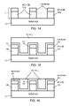
- the structure shown in FIG. 13 is etched down through MTJ/BE layer stack 31 using the hard mask line pattern 32 b to form the hard mask/MTJ/BE lines 51 which include the remaining hard mask 32 c and MTJ/bottom electrode lines 31 b shown in FIG. 14 which shows a cross section perpendicular to the substrate and perpendicular to the long axis of the lines.
- this etching process may use methanol plasma which has a low etch rate of the hard mask layer 32 b compared to the MTJ/BE layers 31 .
- FIG. 15 illustrates a subsequent stage in the process after the stage shown in FIG. 14 , after the MTJ/bottom electrode lines 31 b with the remaining hard mask layer 32 c on top have been encapsulated by first depositing a thin, conformal SiN layer 38 over the wafer to protect the exposed sidewall of the MTJ structure. Over the thin conformal SiN layer 38 , a thicker SiO 2 layer 39 has been deposited to fill in the gaps between the MTJ/bottom electrode lines 31 b and allow planarization.
- the SiO 2 layer 39 is planarized using oxide CMP with the SiN layer 38 functioning as a stop layer for the CMP process.
- the result is SiO 2 fill 39 b between the SiN encapsulation.
- the exposed surface of the wafer has alternating lines of SiO 2 fill 39 b and SiN encapsulation 38 .
- the SiN layer 38 above the hard mask lines 32 c has been removed to expose the top of the hard mask lines 32 c .
- the SiN layer 38 is removed by blanket etching using an appropriate gas chemistry.
- some of the SiO 2 layer 39 b is also removed.
- the exposed surface of the wafer now has alternating lines of SiO 2 fill 39 b , SiN encapsulation 38 and hard mask 32 c .
- a top electrode layer 40 has been deposited on top of the hard mask/MTJ/BE lines 32 c , 31 b and remaining SiO 2 fill layer 39 b and SiN encapsulation layer 38 b.
- FIG. 19 A subsequent stage of the process is illustrated in FIG. 19 .
- the hard mask/MTJ/BE lines 51 are shown as a unit.
- a dielectric layer 41 , a thin metal layer 42 and a BARC layer 43 have been deposited over the top electrode layer 40 .
- the thin metal layer 42 is made of Cu.
- a photoresist mask 44 has been patterned into lines arranged orthogonally to the direction of the hard mask/MTJ/BE lines 51 .
- the dielectric lines 41 b have been formed by etching using photoresist line mask 44 in FIG. 19 .
- the dielectric lines 41 b are then used to form the top electrode lines 40 b by another etching process with the result as shown in FIGS. 21 a and 21 b .
- this etching process may use CF 4 , Cl 2 , BCl 3 plasma or any combination of these with other gases such as Ar, H 2 or O 2 , which has a high etch rate of the top electrode layer material compared to the dielectric layer 41 b .
- FIG. 21 a is an isometric section view that shows the top electrode lines 40 b disposed on the wafer surface.
- 21 b is a plan view looking down between two of the top electrode lines 40 b showing that the exposed surface between the top electrode lines 40 b includes tops of the hard mask 32 c (which is above MTJ/BE 31 b ), the SiO 2 fill 39 b and SiN encapsulation 38 b.
- FIGS. 22 a - c show that the substrate 30 is now exposed where the selected SiO 2 fill 39 b and SiN encapsulation 38 b have been removed.
- FIG. 22 b shows the cross section view through A-A (labeled in FIG. 22 a ) with hard mask/MTJ/BE lines 51 disposed on the substrate 30 .
- FIG. 22 c shows the cross section view through B-B with top electrode lines 40 b disposed SiO 2 fill 39 b and SiN encapsulation 38 b.
- FIGS. 23 a - e A subsequent stage of the process is illustrated in FIGS. 23 a - e .
- the remaining areas of hard mask/MTJ/BE lines not covered by the top electrode line 40 b are removed to form hard mask/MTJ/BE pillars 51 p underneath the top electrode line 40 b as illustrated isometric section view in FIG. 23 e .
- FIG. 23 a is a top plan view that shows that the surface of substrate 30 is now exposed where the selected hard mask/MTJ/BE material has been removed.
- FIG. 23 b shows the cross section view through A-A (labeled in FIG. 23 a ) which now contains only the substrate 30 , which as previously indicated can contain previously patterned circuitry.
- FIG. 23 c shows the cross section view through B-B which has not been changed from that shown in FIG. 22 c .
- FIG. 23 d shows the cross section view through C-C showing hard mask/MTJ/BE pillars 51 p underneath the top electrode line 40 b.
- the hard mask/MTJ/BE element 51 p is patterned as described, a conventional process can be resumed.
- the array of MTJ/BE elements are encapsulated in dielectric material (not shown) and followed by the bitline interconnection process to make electrical contact to the top electrode and providing electrical wiring to the CMOS circuitry in the substrate.
- This embodiment of the invention thus allows for the hard mask/MTJ/BE pillars 51 p to become self-aligned to the top electrode line 40 b.
- a fifth embodiment of the present invention is an alternative of the fourth embodiment in which the self-aligned double patterning (SDP) method as illustrated in FIGS. 10 a - f and described above can be used to create the dielectric line patterns shown in FIG. 4 but with a width F/2 at a spacing of F/2, for example.
- SDP self-aligned double patterning
- a sixth embodiment is an alternative of the fourth embodiment in which the self-aligned double patterning (SDP) method as illustrated in FIGS. 10 a - f a self-aligned double patterning method as illustrated in FIGS. 10 a - f and described above is used to create a each of the first and second the orthogonal line patterns similar to arrive at a structure as shown in FIG. 20 .
- the subsequent process steps are similar to the steps shown in FIG. 21 a to FIG. 23 e and described above but with a width F/2 at a spacing of F/2, for example.
Abstract
Description
Claims (9)
Priority Applications (1)
| Application Number | Priority Date | Filing Date | Title |
|---|---|---|---|
| US13/610,587 US8802451B2 (en) | 2008-02-29 | 2012-09-11 | Method for manufacturing high density non-volatile magnetic memory |
Applications Claiming Priority (2)
| Application Number | Priority Date | Filing Date | Title |
|---|---|---|---|
| US12/040,827 US8535952B2 (en) | 2006-02-25 | 2008-02-29 | Method for manufacturing non-volatile magnetic memory |
| US13/610,587 US8802451B2 (en) | 2008-02-29 | 2012-09-11 | Method for manufacturing high density non-volatile magnetic memory |
Related Parent Applications (1)
| Application Number | Title | Priority Date | Filing Date |
|---|---|---|---|
| US12/040,827 Continuation-In-Part US8535952B2 (en) | 2006-02-25 | 2008-02-29 | Method for manufacturing non-volatile magnetic memory |
Publications (2)
| Publication Number | Publication Date |
|---|---|
| US20130244344A1 US20130244344A1 (en) | 2013-09-19 |
| US8802451B2 true US8802451B2 (en) | 2014-08-12 |
Family
ID=49157994
Family Applications (1)
| Application Number | Title | Priority Date | Filing Date |
|---|---|---|---|
| US13/610,587 Active 2028-03-22 US8802451B2 (en) | 2008-02-29 | 2012-09-11 | Method for manufacturing high density non-volatile magnetic memory |
Country Status (1)
| Country | Link |
|---|---|
| US (1) | US8802451B2 (en) |
Cited By (46)
| Publication number | Priority date | Publication date | Assignee | Title |
|---|---|---|---|---|
| US20140151826A1 (en) * | 2011-05-27 | 2014-06-05 | University Of North Texsas | Graphene magnetic tunnel junction spin filters and methods of making |
| US20140319634A1 (en) * | 2013-04-28 | 2014-10-30 | Alexander Mikhailovich Shukh | High Density Nonvolatile Memory |
| US20150243518A1 (en) * | 2014-02-23 | 2015-08-27 | Tokyo Electron Limited | Method for multiplying pattern density by crossing multiple patterned layers |
| US9281168B2 (en) * | 2014-06-06 | 2016-03-08 | Everspin Technologies, Inc. | Reducing switching variation in magnetoresistive devices |
| US9412786B1 (en) * | 2014-10-02 | 2016-08-09 | Everspin Technologies, Inc. | Magnetoresistive device design and process integration with surrounding circuitry |
| US10056543B2 (en) | 2015-08-19 | 2018-08-21 | Samsung Electronics Co., Ltd. | Magnetoresistive random access memory device having magnetic tunnel junction and method of manufacturing the same |
| US10199270B2 (en) * | 2017-05-25 | 2019-02-05 | Globalfoundries Inc. | Multi-directional self-aligned multiple patterning |
| US20190207107A1 (en) * | 2017-12-30 | 2019-07-04 | Spin Memory, Inc | Method for manufacturing reduced pitch magnetic random access memory pillar |
| US10347314B2 (en) | 2015-08-14 | 2019-07-09 | Spin Memory, Inc. | Method and apparatus for bipolar memory write-verify |
| US10360964B2 (en) | 2016-09-27 | 2019-07-23 | Spin Memory, Inc. | Method of writing contents in memory during a power up sequence using a dynamic redundancy register in a memory device |
| US10360962B1 (en) | 2017-12-28 | 2019-07-23 | Spin Memory, Inc. | Memory array with individually trimmable sense amplifiers |
| US10366774B2 (en) | 2016-09-27 | 2019-07-30 | Spin Memory, Inc. | Device with dynamic redundancy registers |
| US10395711B2 (en) | 2017-12-28 | 2019-08-27 | Spin Memory, Inc. | Perpendicular source and bit lines for an MRAM array |
| US10395712B2 (en) | 2017-12-28 | 2019-08-27 | Spin Memory, Inc. | Memory array with horizontal source line and sacrificial bitline per virtual source |
| US10411185B1 (en) | 2018-05-30 | 2019-09-10 | Spin Memory, Inc. | Process for creating a high density magnetic tunnel junction array test platform |
| US10437723B2 (en) | 2016-09-27 | 2019-10-08 | Spin Memory, Inc. | Method of flushing the contents of a dynamic redundancy register to a secure storage area during a power down in a memory device |
| US10437491B2 (en) | 2016-09-27 | 2019-10-08 | Spin Memory, Inc. | Method of processing incomplete memory operations in a memory device during a power up sequence and a power down sequence using a dynamic redundancy register |
| US10446744B2 (en) | 2018-03-08 | 2019-10-15 | Spin Memory, Inc. | Magnetic tunnel junction wafer adaptor used in magnetic annealing furnace and method of using the same |
| US10481976B2 (en) | 2017-10-24 | 2019-11-19 | Spin Memory, Inc. | Forcing bits as bad to widen the window between the distributions of acceptable high and low resistive bits thereby lowering the margin and increasing the speed of the sense amplifiers |
| US10489245B2 (en) | 2017-10-24 | 2019-11-26 | Spin Memory, Inc. | Forcing stuck bits, waterfall bits, shunt bits and low TMR bits to short during testing and using on-the-fly bit failure detection and bit redundancy remapping techniques to correct them |
| US10529439B2 (en) | 2017-10-24 | 2020-01-07 | Spin Memory, Inc. | On-the-fly bit failure detection and bit redundancy remapping techniques to correct for fixed bit defects |
| US10529915B2 (en) | 2018-03-23 | 2020-01-07 | Spin Memory, Inc. | Bit line structures for three-dimensional arrays with magnetic tunnel junction devices including an annular free magnetic layer and a planar reference magnetic layer |
| US10546624B2 (en) | 2017-12-29 | 2020-01-28 | Spin Memory, Inc. | Multi-port random access memory |
| US10546625B2 (en) | 2016-09-27 | 2020-01-28 | Spin Memory, Inc. | Method of optimizing write voltage based on error buffer occupancy |
| US10593396B2 (en) | 2018-07-06 | 2020-03-17 | Spin Memory, Inc. | Multi-bit cell read-out techniques for MRAM cells with mixed pinned magnetization orientations |
| US10593870B2 (en) | 2017-12-14 | 2020-03-17 | International Business Machines Corporation | Sidewall image transfer on magnetic tunnel junction stack for magnetoresistive random-access memory patterning |
| US10600478B2 (en) | 2018-07-06 | 2020-03-24 | Spin Memory, Inc. | Multi-bit cell read-out techniques for MRAM cells with mixed pinned magnetization orientations |
| US10650875B2 (en) | 2018-08-21 | 2020-05-12 | Spin Memory, Inc. | System for a wide temperature range nonvolatile memory |
| US10656994B2 (en) | 2017-10-24 | 2020-05-19 | Spin Memory, Inc. | Over-voltage write operation of tunnel magnet-resistance (“TMR”) memory device and correcting failure bits therefrom by using on-the-fly bit failure detection and bit redundancy remapping techniques |
| US10756259B2 (en) * | 2018-11-20 | 2020-08-25 | Applied Materials, Inc. | Spin orbit torque MRAM and manufacture thereof |
| US10784437B2 (en) | 2018-03-23 | 2020-09-22 | Spin Memory, Inc. | Three-dimensional arrays with MTJ devices including a free magnetic trench layer and a planar reference magnetic layer |
| US10818331B2 (en) | 2016-09-27 | 2020-10-27 | Spin Memory, Inc. | Multi-chip module for MRAM devices with levels of dynamic redundancy registers |
| US10840439B2 (en) | 2017-12-29 | 2020-11-17 | Spin Memory, Inc. | Magnetic tunnel junction (MTJ) fabrication methods and systems |
| US10879453B2 (en) * | 2016-11-02 | 2020-12-29 | Nanosc Ab | Spin oscillator device and mutually synchronized spin oscillator device arrays |
| US10886330B2 (en) | 2017-12-29 | 2021-01-05 | Spin Memory, Inc. | Memory device having overlapping magnetic tunnel junctions in compliance with a reference pitch |
| US10891997B2 (en) | 2017-12-28 | 2021-01-12 | Spin Memory, Inc. | Memory array with horizontal source line and a virtual source line |
| US10971680B2 (en) | 2018-10-01 | 2021-04-06 | Spin Memory, Inc. | Multi terminal device stack formation methods |
| US11107979B2 (en) | 2018-12-28 | 2021-08-31 | Spin Memory, Inc. | Patterned silicide structures and methods of manufacture |
| US11107974B2 (en) | 2018-03-23 | 2021-08-31 | Spin Memory, Inc. | Magnetic tunnel junction devices including a free magnetic trench layer and a planar reference magnetic layer |
| US11107978B2 (en) | 2018-03-23 | 2021-08-31 | Spin Memory, Inc. | Methods of manufacturing three-dimensional arrays with MTJ devices including a free magnetic trench layer and a planar reference magnetic layer |
| US11145808B2 (en) * | 2019-11-12 | 2021-10-12 | Applied Materials, Inc. | Methods for etching a structure for MRAM applications |
| US11152563B2 (en) | 2019-08-29 | 2021-10-19 | International Business Machines Corporation | Reinforced single element bottom electrode for MTJ-containing devices |
| US11195995B2 (en) | 2020-01-06 | 2021-12-07 | International Business Machines Corporation | Back-end-of-line compatible processing for forming an array of pillars |
| US20220181544A1 (en) * | 2020-12-09 | 2022-06-09 | International Business Machines Corporation | Multi-state sot-mram structure |
| US11476415B2 (en) | 2018-11-30 | 2022-10-18 | International Business Machines Corporation | Patterning magnetic tunnel junctions and the like while reducing detrimental resputtering of underlying features |
| US11621293B2 (en) | 2018-10-01 | 2023-04-04 | Integrated Silicon Solution, (Cayman) Inc. | Multi terminal device stack systems and methods |
Families Citing this family (80)
| Publication number | Priority date | Publication date | Assignee | Title |
|---|---|---|---|---|
| KR101215951B1 (en) * | 2011-03-24 | 2013-01-21 | 에스케이하이닉스 주식회사 | Semiconductor Memory And Manufacturing Method Thereof |
| KR20130015145A (en) * | 2011-08-02 | 2013-02-13 | 삼성전자주식회사 | Method of forming fine patterns for semiconductor device |
| US8747680B1 (en) | 2012-08-14 | 2014-06-10 | Everspin Technologies, Inc. | Method of manufacturing a magnetoresistive-based device |
| US20140061827A1 (en) * | 2012-08-29 | 2014-03-06 | Headway Technologies, Inc. | Metal Protection Layer over SiN Encapsulation for Spin-Torque MRAM Device Applications |
| CN104465984B (en) * | 2013-09-17 | 2017-08-25 | 中芯国际集成电路制造(北京)有限公司 | MTJ and forming method thereof |
| US9263667B1 (en) * | 2014-07-25 | 2016-02-16 | Spin Transfer Technologies, Inc. | Method for manufacturing MTJ memory device |
| US9337412B2 (en) | 2014-09-22 | 2016-05-10 | Spin Transfer Technologies, Inc. | Magnetic tunnel junction structure for MRAM device |
| US9502642B2 (en) * | 2015-04-10 | 2016-11-22 | Micron Technology, Inc. | Magnetic tunnel junctions, methods used while forming magnetic tunnel junctions, and methods of forming magnetic tunnel junctions |
| US10468590B2 (en) | 2015-04-21 | 2019-11-05 | Spin Memory, Inc. | High annealing temperature perpendicular magnetic anisotropy structure for magnetic random access memory |
| US9728712B2 (en) | 2015-04-21 | 2017-08-08 | Spin Transfer Technologies, Inc. | Spin transfer torque structure for MRAM devices having a spin current injection capping layer |
| US9960346B2 (en) | 2015-05-07 | 2018-05-01 | Micron Technology, Inc. | Magnetic tunnel junctions |
| US9853206B2 (en) | 2015-06-16 | 2017-12-26 | Spin Transfer Technologies, Inc. | Precessional spin current structure for MRAM |
| US9362490B1 (en) * | 2015-07-09 | 2016-06-07 | Rongfu Xiao | Method of patterning MTJ cell without sidewall damage |
| US9773974B2 (en) | 2015-07-30 | 2017-09-26 | Spin Transfer Technologies, Inc. | Polishing stop layer(s) for processing arrays of semiconductor elements |
| US9780143B2 (en) * | 2015-08-25 | 2017-10-03 | Western Digital Technologies, Inc. | Implementing magnetic memory integration with CMOS driving circuits |
| US10522402B2 (en) | 2015-12-16 | 2019-12-31 | Intel Corporation | Grid self-aligned metal via processing schemes for back end of line (BEOL) interconnects and structures resulting therefrom |
| JP6499980B2 (en) * | 2016-01-04 | 2019-04-10 | 株式会社日立ハイテクノロジーズ | Plasma processing method |
| US9741926B1 (en) | 2016-01-28 | 2017-08-22 | Spin Transfer Technologies, Inc. | Memory cell having magnetic tunnel junction and thermal stability enhancement layer |
| US9779943B2 (en) | 2016-02-25 | 2017-10-03 | Globalfoundries Inc. | Compensating for lithographic limitations in fabricating semiconductor interconnect structures |
| US9818623B2 (en) | 2016-03-22 | 2017-11-14 | Globalfoundries Inc. | Method of forming a pattern for interconnection lines and associated continuity blocks in an integrated circuit |
| US9679809B1 (en) * | 2016-03-22 | 2017-06-13 | Globalfoundries Inc. | Method of forming self aligned continuity blocks for mandrel and non-mandrel interconnect lines |
| US9691626B1 (en) | 2016-03-22 | 2017-06-27 | Globalfoundries Inc. | Method of forming a pattern for interconnection lines in an integrated circuit wherein the pattern includes gamma and beta block mask portions |
| US9691775B1 (en) | 2016-04-28 | 2017-06-27 | Globalfoundries Inc. | Combined SADP fins for semiconductor devices and methods of making the same |
| US9680089B1 (en) | 2016-05-13 | 2017-06-13 | Micron Technology, Inc. | Magnetic tunnel junctions |
| US9818640B1 (en) | 2016-09-21 | 2017-11-14 | Globalfoundries Inc. | Apparatus and method of forming self-aligned cuts in a non-mandrel line of an array of metal lines |
| US9818641B1 (en) | 2016-09-21 | 2017-11-14 | Globalfoundries Inc. | Apparatus and method of forming self-aligned cuts in mandrel and a non-mandrel lines of an array of metal lines |
| US9786545B1 (en) | 2016-09-21 | 2017-10-10 | Globalfoundries Inc. | Method of forming ANA regions in an integrated circuit |
| US10460781B2 (en) | 2016-09-27 | 2019-10-29 | Spin Memory, Inc. | Memory device with a dual Y-multiplexer structure for performing two simultaneous operations on the same row of a memory bank |
| US11119910B2 (en) | 2016-09-27 | 2021-09-14 | Spin Memory, Inc. | Heuristics for selecting subsegments for entry in and entry out operations in an error cache system with coarse and fine grain segments |
| US10446210B2 (en) | 2016-09-27 | 2019-10-15 | Spin Memory, Inc. | Memory instruction pipeline with a pre-read stage for a write operation for reducing power consumption in a memory device that uses dynamic redundancy registers |
| US10628316B2 (en) | 2016-09-27 | 2020-04-21 | Spin Memory, Inc. | Memory device with a plurality of memory banks where each memory bank is associated with a corresponding memory instruction pipeline and a dynamic redundancy register |
| US10991410B2 (en) | 2016-09-27 | 2021-04-27 | Spin Memory, Inc. | Bi-polar write scheme |
| US11119936B2 (en) | 2016-09-27 | 2021-09-14 | Spin Memory, Inc. | Error cache system with coarse and fine segments for power optimization |
| US11151042B2 (en) | 2016-09-27 | 2021-10-19 | Integrated Silicon Solution, (Cayman) Inc. | Error cache segmentation for power reduction |
| US10586914B2 (en) | 2016-10-14 | 2020-03-10 | Applied Materials, Inc. | Method of forming ultra-smooth bottom electrode surface for depositing magnetic tunnel junctions |
| US9852986B1 (en) | 2016-11-28 | 2017-12-26 | Globalfoundries Inc. | Method of patterning pillars to form variable continuity cuts in interconnection lines of an integrated circuit |
| US10002786B1 (en) | 2016-12-15 | 2018-06-19 | Globalfoundries Inc. | Interconnection cells having variable width metal lines and fully-self aligned variable length continuity cuts |
| US10043703B2 (en) | 2016-12-15 | 2018-08-07 | Globalfoundries Inc. | Apparatus and method for forming interconnection lines having variable pitch and variable widths |
| US9887127B1 (en) | 2016-12-15 | 2018-02-06 | Globalfoundries Inc. | Interconnection lines having variable widths and partially self-aligned continuity cuts |
| US9812351B1 (en) | 2016-12-15 | 2017-11-07 | Globalfoundries Inc. | Interconnection cells having variable width metal lines and fully-self aligned continuity cuts |
| US20180233662A1 (en) * | 2017-02-14 | 2018-08-16 | Lam Research Corporation | Systems and methods for patterning of high density standalone mram devices |
| US10665777B2 (en) | 2017-02-28 | 2020-05-26 | Spin Memory, Inc. | Precessional spin current structure with non-magnetic insertion layer for MRAM |
| US10672976B2 (en) | 2017-02-28 | 2020-06-02 | Spin Memory, Inc. | Precessional spin current structure with high in-plane magnetization for MRAM |
| US10032978B1 (en) | 2017-06-27 | 2018-07-24 | Spin Transfer Technologies, Inc. | MRAM with reduced stray magnetic fields |
| WO2019040504A2 (en) | 2017-08-23 | 2019-02-28 | Everspin Technologies, Inc. | Methods of manufacturing integrated circuit using encapsulation during an etch process |
| WO2019046064A1 (en) * | 2017-08-29 | 2019-03-07 | Everspin Technologies, Inc. | Method of etching magnetoresistive stack |
| US10679685B2 (en) | 2017-12-27 | 2020-06-09 | Spin Memory, Inc. | Shared bit line array architecture for magnetoresistive memory |
| US10811594B2 (en) * | 2017-12-28 | 2020-10-20 | Spin Memory, Inc. | Process for hard mask development for MRAM pillar formation using photolithography |
| US10424726B2 (en) | 2017-12-28 | 2019-09-24 | Spin Memory, Inc. | Process for improving photoresist pillar adhesion during MRAM fabrication |
| US10516094B2 (en) | 2017-12-28 | 2019-12-24 | Spin Memory, Inc. | Process for creating dense pillars using multiple exposures for MRAM fabrication |
| US20190207101A1 (en) * | 2017-12-28 | 2019-07-04 | Spin Transfer Technologies, Inc. | Photolithographic method for fabricating dense pillar arrays using spacers as a pattern |
| US10199083B1 (en) | 2017-12-29 | 2019-02-05 | Spin Transfer Technologies, Inc. | Three-terminal MRAM with ac write-assist for low read disturb |
| US10236048B1 (en) | 2017-12-29 | 2019-03-19 | Spin Memory, Inc. | AC current write-assist in orthogonal STT-MRAM |
| US10236047B1 (en) | 2017-12-29 | 2019-03-19 | Spin Memory, Inc. | Shared oscillator (STNO) for MRAM array write-assist in orthogonal STT-MRAM |
| US10840436B2 (en) | 2017-12-29 | 2020-11-17 | Spin Memory, Inc. | Perpendicular magnetic anisotropy interface tunnel junction devices and methods of manufacture |
| US10270027B1 (en) | 2017-12-29 | 2019-04-23 | Spin Memory, Inc. | Self-generating AC current assist in orthogonal STT-MRAM |
| US10784439B2 (en) | 2017-12-29 | 2020-09-22 | Spin Memory, Inc. | Precessional spin current magnetic tunnel junction devices and methods of manufacture |
| US10360961B1 (en) | 2017-12-29 | 2019-07-23 | Spin Memory, Inc. | AC current pre-charge write-assist in orthogonal STT-MRAM |
| US10367139B2 (en) | 2017-12-29 | 2019-07-30 | Spin Memory, Inc. | Methods of manufacturing magnetic tunnel junction devices |
| US10424723B2 (en) | 2017-12-29 | 2019-09-24 | Spin Memory, Inc. | Magnetic tunnel junction devices including an optimization layer |
| US10236439B1 (en) | 2017-12-30 | 2019-03-19 | Spin Memory, Inc. | Switching and stability control for perpendicular magnetic tunnel junction device |
| US10339993B1 (en) | 2017-12-30 | 2019-07-02 | Spin Memory, Inc. | Perpendicular magnetic tunnel junction device with skyrmionic assist layers for free layer switching |
| US10141499B1 (en) | 2017-12-30 | 2018-11-27 | Spin Transfer Technologies, Inc. | Perpendicular magnetic tunnel junction device with offset precessional spin current layer |
| US10255962B1 (en) | 2017-12-30 | 2019-04-09 | Spin Memory, Inc. | Microwave write-assist in orthogonal STT-MRAM |
| US10229724B1 (en) | 2017-12-30 | 2019-03-12 | Spin Memory, Inc. | Microwave write-assist in series-interconnected orthogonal STT-MRAM devices |
| US10319900B1 (en) | 2017-12-30 | 2019-06-11 | Spin Memory, Inc. | Perpendicular magnetic tunnel junction device with precessional spin current layer having a modulated moment density |
| US10468588B2 (en) | 2018-01-05 | 2019-11-05 | Spin Memory, Inc. | Perpendicular magnetic tunnel junction device with skyrmionic enhancement layers for the precessional spin current magnetic layer |
| US10438996B2 (en) | 2018-01-08 | 2019-10-08 | Spin Memory, Inc. | Methods of fabricating magnetic tunnel junctions integrated with selectors |
| US10438995B2 (en) | 2018-01-08 | 2019-10-08 | Spin Memory, Inc. | Devices including magnetic tunnel junctions integrated with selectors |
| US10431628B2 (en) * | 2018-01-09 | 2019-10-01 | Spin Memory, Inc. | Dual channel/gate vertical field-effect transistor (FET) for use with a perpendicular magnetic tunnel junction (PMTJ) |
| US10840440B2 (en) | 2018-02-22 | 2020-11-17 | Taiwan Semiconductor Manufacturing Company, Ltd. | Metal/dielectric/metal hybrid hard mask to define ultra-large height top electrode for sub 60nm MRAM devices |
| US10388861B1 (en) | 2018-03-08 | 2019-08-20 | Spin Memory, Inc. | Magnetic tunnel junction wafer adaptor used in magnetic annealing furnace and method of using the same |
| US10692569B2 (en) | 2018-07-06 | 2020-06-23 | Spin Memory, Inc. | Read-out techniques for multi-bit cells |
| US10559338B2 (en) | 2018-07-06 | 2020-02-11 | Spin Memory, Inc. | Multi-bit cell read-out techniques |
| US10699761B2 (en) | 2018-09-18 | 2020-06-30 | Spin Memory, Inc. | Word line decoder memory architecture |
| US10580827B1 (en) | 2018-11-16 | 2020-03-03 | Spin Memory, Inc. | Adjustable stabilizer/polarizer method for MRAM with enhanced stability and efficient switching |
| CN112563409A (en) * | 2019-09-10 | 2021-03-26 | 浙江驰拓科技有限公司 | Magnetic memory based on spin orbit torque and preparation method thereof |
| CN112820821A (en) * | 2019-11-15 | 2021-05-18 | 联华电子股份有限公司 | Semiconductor element and manufacturing method thereof |
| US11366182B2 (en) * | 2020-01-24 | 2022-06-21 | Vanguard International Semiconductor Corporation | Magnetoresistive devices and methods for forming the same |
| US11417832B2 (en) * | 2020-08-31 | 2022-08-16 | Taiwan Semiconductor Manufacturing Company Ltd. | Semiconductor device and manufacturing method thereof |
Citations (96)
| Publication number | Priority date | Publication date | Assignee | Title |
|---|---|---|---|---|
| US3665264A (en) | 1969-09-01 | 1972-05-23 | Matsushita Electric Ind Co Ltd | Stress sensitive semiconductor element having an n+pp+or p+nn+junction |
| US5060098A (en) | 1988-04-18 | 1991-10-22 | Hitachi, Ltd. | Magnetic recorder provided with a magnetic head slider having a non-magnetic oxide of spinel structure |
| US5695864A (en) | 1995-09-28 | 1997-12-09 | International Business Machines Corporation | Electronic device using magnetic components |
| US6072718A (en) | 1998-02-10 | 2000-06-06 | International Business Machines Corporation | Magnetic memory devices having multiple magnetic tunnel junctions therein |
| US6169689B1 (en) | 1999-12-08 | 2001-01-02 | Motorola, Inc. | MTJ stacked cell memory sensing method and apparatus |
| US6285581B1 (en) | 1999-12-13 | 2001-09-04 | Motorola, Inc. | MRAM having semiconductor device integrated therein |
| US6365419B1 (en) | 2000-08-28 | 2002-04-02 | Motorola, Inc. | High density MRAM cell array |
| US20020048128A1 (en) | 2000-10-20 | 2002-04-25 | Kabushiki Kaisha Toshiba | Magnetoresistance effect element, magnetic head and magnetic recording and/or reproducing system |
| JP2002197851A (en) | 2000-12-25 | 2002-07-12 | Toshiba Corp | Magnetic random access memory |
| US6421270B1 (en) | 2000-12-29 | 2002-07-16 | Amic Technology (Taiwan) Inc. | Magneto-resistive random access memory |
| US6469926B1 (en) | 2000-03-22 | 2002-10-22 | Motorola, Inc. | Magnetic element with an improved magnetoresistance ratio and fabricating method thereof |
| US6501139B1 (en) | 2001-03-30 | 2002-12-31 | Matrix Semiconductor, Inc. | High-voltage transistor and fabrication process |
| US20030108776A1 (en) | 2001-12-06 | 2003-06-12 | Seagate Technology Llc | Pseudo-laminated soft underlayers for perpendicular magnetic recording media |
| US20030123200A1 (en) | 2001-12-27 | 2003-07-03 | Fujitsu Limited | Magnetoresistive element |
| US6590806B1 (en) | 2000-03-09 | 2003-07-08 | Hewlett-Packard Development Company, L.P. | Multibit magnetic memory element |
| US20030128483A1 (en) | 2001-10-12 | 2003-07-10 | Nec Corporation | Exchange coupling film, magneto-resistance effect device, magnetic head, and magnetic random access memory |
| US6603677B2 (en) | 2000-12-07 | 2003-08-05 | Commissariat A L'energie Atomique | Three-layered stacked magnetic spin polarization device with memory |
| US20030180776A1 (en) | 2002-02-21 | 2003-09-25 | Ming Wu | Detection by sliding template amplification |
| US6639312B2 (en) | 2001-11-07 | 2003-10-28 | Matrix Semiconductor, Inc | Dummy wafers and methods for making the same |
| US6642595B1 (en) | 2002-07-29 | 2003-11-04 | Industrial Technology Research Institute | Magnetic random access memory with low writing current |
| US6649451B1 (en) | 2001-02-02 | 2003-11-18 | Matrix Semiconductor, Inc. | Structure and method for wafer comprising dielectric and semiconductor |
| US20030232223A1 (en) | 1994-08-25 | 2003-12-18 | Johna Leddy | Methods for forming magnetically modified electrodes and articles produced thereby |
| US6670660B2 (en) | 2000-09-28 | 2003-12-30 | Kabushiki Kaisha Toshiba | Semiconductor memory device utilizing tunnel magneto resistive effects and method for manufacturing the same |
| JP2004006774A (en) | 2002-03-29 | 2004-01-08 | Toshiba Corp | Solid magnetic element and solid magnetic element array |
| US6697294B1 (en) | 2001-02-23 | 2004-02-24 | Western Digital (Fremont), Inc. | Designs of reference cells for magnetic tunnel junction (MTJ) MRAM |
| US20040042128A1 (en) | 2002-08-30 | 2004-03-04 | Slaughter Jon M. | Nanocrystalline layers for improved MRAM tunnel junctions |
| US6714444B2 (en) | 2002-08-06 | 2004-03-30 | Grandis, Inc. | Magnetic element utilizing spin transfer and an MRAM device using the magnetic element |
| US6716644B2 (en) * | 2002-05-17 | 2004-04-06 | Micron Technology, Inc. | Method for forming MRAM bit having a bottom sense layer utilizing electroless plating |
| US6724585B2 (en) | 1998-09-18 | 2004-04-20 | Nec Corporation | Magnetoresistive element and device utilizing magnetoresistance effect |
| US6744086B2 (en) | 2001-05-15 | 2004-06-01 | Nve Corporation | Current switched magnetoresistive memory cell |
| US6743642B2 (en) | 2002-11-06 | 2004-06-01 | International Business Machines Corporation | Bilayer CMP process to improve surface roughness of magnetic stack in MRAM technology |
| US6759263B2 (en) | 2002-08-29 | 2004-07-06 | Chentsau Ying | Method of patterning a layer of magnetic material |
| US20040130936A1 (en) | 2003-01-07 | 2004-07-08 | Grandis Inc. | Spin-transfer multilayer stack containing magnetic layers with resettable magnetization |
| US20040159832A1 (en) | 2003-01-31 | 2004-08-19 | Hack Jonathan A. | Spintonic devices and methods of making spintronic devices |
| US6780652B2 (en) * | 2001-03-15 | 2004-08-24 | Micron Technology, Inc. | Self-aligned MRAM contact and method of fabrication |
| US6783999B1 (en) | 2003-06-20 | 2004-08-31 | Infineon Technologies Ag | Subtractive stud formation for MRAM manufacturing |
| US6785159B2 (en) * | 2002-08-29 | 2004-08-31 | Micron Technology, Inc. | Combination etch stop and in situ resistor in a magnetoresistive memory and methods for fabricating same |
| US20040170055A1 (en) | 2003-02-28 | 2004-09-02 | Frank Albert | Magnetostatically coupled magnetic elements utilizing spin transfer and an MRAM device using the magnetic element |
| US20040201070A1 (en) | 2003-04-09 | 2004-10-14 | Deak James G | Self-aligned, low-resistance, efficient MRAM read/write conductors |
| US6821907B2 (en) | 2002-03-06 | 2004-11-23 | Applied Materials Inc | Etching methods for a magnetic memory cell stack |
| US20050045913A1 (en) | 2003-08-26 | 2005-03-03 | Nguyen Paul P. | Magnetic memory element utilizing spin transfer switching and storing multiple bits |
| US20050063222A1 (en) | 2003-09-19 | 2005-03-24 | Yiming Huai | Current confined pass layer for magnetic elements utilizing spin-transfer and an MRAM device using such magnetic elements |
| US6893893B2 (en) | 2002-03-19 | 2005-05-17 | Applied Materials Inc | Method of preventing short circuits in magnetic film stacks |
| US20050105325A1 (en) | 2003-09-29 | 2005-05-19 | Kabushiki Kaisha Toshiba | Magnetic cell and magnetic memory |
| US6905578B1 (en) | 1998-04-27 | 2005-06-14 | Cvc Products, Inc. | Apparatus and method for multi-target physical-vapor deposition of a multi-layer material structure |
| US20050167657A1 (en) | 2000-03-09 | 2005-08-04 | Nickel Janice H. | Multi-bit magnetic memory cells |
| US6933155B2 (en) | 2003-05-21 | 2005-08-23 | Grandis, Inc. | Methods for providing a sub .15 micron magnetic memory structure |
| US20050195532A1 (en) | 2004-03-03 | 2005-09-08 | Kabushiki Kaisha Toshiba | Magneto-resistance effect element and magnetic memory |
| US20050201020A1 (en) | 2004-03-11 | 2005-09-15 | Hiromi Fuke | Magnetoresistive element, magnetic head, and magnetic recording and reproducing apparatus |
| US20050207219A1 (en) | 2003-03-03 | 2005-09-22 | Kyu-Mann Lee | Magnetic tunnel junction structures and methods of fabrication |
| US6964928B2 (en) | 2002-08-29 | 2005-11-15 | Chentsau Ying | Method for removing residue from a magneto-resistive random access memory (MRAM) film stack using a dual mask |
| US20050254287A1 (en) | 2004-05-11 | 2005-11-17 | Thierry Valet | Spin barrier enhanced magnetoresistance effect element and magnetic memory using the same |
| US6984529B2 (en) | 2003-09-10 | 2006-01-10 | Infineon Technologies Ag | Fabrication process for a magnetic tunnel junction device |
| US6984561B2 (en) | 2002-12-19 | 2006-01-10 | Matrix Semiconductor, Inc. | Method for making high density nonvolatile memory |
| US6984585B2 (en) | 2002-08-12 | 2006-01-10 | Applied Materials Inc | Method for removal of residue from a magneto-resistive random access memory (MRAM) film stack using a sacrificial mask layer |
| US20060017081A1 (en) | 2004-07-26 | 2006-01-26 | Jijun Sun | Magnetic tunnel junction element structures and methods for fabricating the same |
| US6992359B2 (en) | 2004-02-26 | 2006-01-31 | Grandis, Inc. | Spin transfer magnetic element with free layers having high perpendicular anisotropy and in-plane equilibrium magnetization |
| US7002781B2 (en) | 2002-09-09 | 2006-02-21 | Fujitsu Limited | Current-perpendicular-to-the-plane structure magnetoresistive element having the free and/or pinned layers being made of a granular film which includes an electrically conductive magnetic material and a dielectric material |
| US7005730B2 (en) | 2002-02-19 | 2006-02-28 | Matrix Semiconductor, Inc. | Memory module having interconnected and stacked integrated circuits |
| US7009877B1 (en) | 2003-11-14 | 2006-03-07 | Grandis, Inc. | Three-terminal magnetostatically coupled spin transfer-based MRAM cell |
| US7018878B2 (en) | 2001-11-07 | 2006-03-28 | Matrix Semiconductor, Inc. | Metal structures for integrated circuits and methods for making the same |
| US7023739B2 (en) | 2003-12-05 | 2006-04-04 | Matrix Semiconductor, Inc. | NAND memory array incorporating multiple write pulse programming of individual memory cells and method for operation of same |
| US7023725B2 (en) | 2002-09-30 | 2006-04-04 | Kabushiki Kaisha Toshiba | Magnetic memory |
| US7026673B2 (en) | 2003-12-11 | 2006-04-11 | International Business Machines Corporation | Low magnetization materials for high performance magnetic memory devices |
| US20060083056A1 (en) | 2002-11-12 | 2006-04-20 | Nve Corporation | Magnetic memory layers thermal pulse transitions |
| US20060104110A1 (en) | 2004-11-18 | 2006-05-18 | International Business Machines Corporation | Spin-current switchable magnetic memory element and method of fabricating the memory element |
| US20060109591A1 (en) | 2004-11-19 | 2006-05-25 | Ranjan Rajiv Y | Method of making substrates for media used in hard drives |
| US20060114620A1 (en) | 2004-11-30 | 2006-06-01 | Tdk Corporation | Granular type free layer and magnetic head |
| US7057921B2 (en) | 2004-05-11 | 2006-06-06 | Grandis, Inc. | Spin barrier enhanced dual magnetoresistance effect element and magnetic memory using the same |
| US20060141640A1 (en) | 2004-12-29 | 2006-06-29 | Yiming Huai | MTJ elements with high spin polarization layers configured for spin-transfer switching and spintronics devices using the magnetic elements |
| US20060171198A1 (en) | 2005-01-28 | 2006-08-03 | Yoshiaki Saito | Spin-injection magnetic random access memory |
| US20060187703A1 (en) | 2002-06-20 | 2006-08-24 | Sony Corporation | Magnetoresistive effect element, magentic memory device and manufacturing method of magnetoresistive effect element and magnetic memory device |
| US20060192237A1 (en) | 2003-12-22 | 2006-08-31 | Yiming Huai | Magnetic elements with ballistic magnetoresistance utilizing spin-transfer and an MRAM device using such magnetic elements |
| US7109539B2 (en) | 2004-03-09 | 2006-09-19 | International Business Machines Corporation | Multiple-bit magnetic random access memory cell employing adiabatic switching |
| JP2006269530A (en) | 2005-03-22 | 2006-10-05 | Toshiba Corp | Magneto-resistance effect element and magnetic memory |
| US7120049B2 (en) | 2002-11-26 | 2006-10-10 | Kabushiki Kaisha Toshiba | Magnetic cell and magnetic memory |
| JP2006277864A (en) | 2005-03-30 | 2006-10-12 | Toshiba Corp | Magnetic disk drive |
| US7123498B2 (en) | 2001-01-24 | 2006-10-17 | International Business Machines Corporation | Non-volatile memory device |
| US7122386B1 (en) | 2005-09-21 | 2006-10-17 | Magic Technologies, Inc. | Method of fabricating contact pad for magnetic random access memory |
| US7126201B2 (en) | 2002-07-09 | 2006-10-24 | Nec Corporation | Magnetic random access memory |
| US20060239066A1 (en) | 2005-04-22 | 2006-10-26 | Taiwan Semiconductor Manufacturing Company, Ltd. | Magnetic random access memory device |
| JP2006295198A (en) | 2005-04-14 | 2006-10-26 | Headway Technologies Inc | Magnetic tunnel junction element, method of forming the same, magnetic memory cell, and method of manufacturing the same |
| US20060268604A1 (en) | 2005-05-25 | 2006-11-30 | Hitachi, Ltd. | Magnetic recording apparatus using magnetization reversal by spin injection with thermal assistance |
| US7148531B2 (en) | 2004-04-29 | 2006-12-12 | Nve Corporation | Magnetoresistive memory SOI cell |
| US20070007609A1 (en) | 2005-07-06 | 2007-01-11 | Kabushiki Kaisha Toshiba | Magnetoresistive effect element and magnetic memory |
| US7170775B2 (en) | 2005-01-06 | 2007-01-30 | Taiwan Semiconductor Manufacturing Company, Ltd. | MRAM cell with reduced write current |
| US7183130B2 (en) | 2003-07-29 | 2007-02-27 | International Business Machines Corporation | Magnetic random access memory and method of fabricating thereof |
| JP2007073971A (en) | 2005-09-07 | 2007-03-22 | Magic Technologies Inc | Magnetic memory cell and method of manufacturing same |
| JP2007096105A (en) | 2005-09-29 | 2007-04-12 | Toshiba Corp | Magnetoresistance effect element, magnetoresistance effect head, magnetic storage device and magnetic memory |
| US20070085068A1 (en) | 2005-10-14 | 2007-04-19 | Dmytro Apalkov | Spin transfer based magnetic storage cells utilizing granular free layers and magnetic memories using such cells |
| US7211446B2 (en) | 2004-06-11 | 2007-05-01 | International Business Machines Corporation | Method of patterning a magnetic tunnel junction stack for a magneto-resistive random access memory |
| JP2007142364A (en) | 2005-10-19 | 2007-06-07 | Toshiba Corp | Magnetoresistance effect element, magnetic random access memory, electronic card and electronic device |
| US20070164336A1 (en) | 2006-01-17 | 2007-07-19 | Yoshiaki Saito | Spin fet and spin memory |
| US20080043519A1 (en) | 2006-08-21 | 2008-02-21 | Kabushiki Kaisha Toshiba | Magnetic memory element, magnetic memory having said magnetic memory element, and method for driving magnetic memory |
| US20100327248A1 (en) * | 2009-06-29 | 2010-12-30 | Seagate Technology Llc | Cell patterning with multiple hard masks |
| US7863060B2 (en) | 2009-03-23 | 2011-01-04 | Magic Technologies, Inc. | Method of double patterning and etching magnetic tunnel junction structures for spin-transfer torque MRAM devices |
-
2012
- 2012-09-11 US US13/610,587 patent/US8802451B2/en active Active
Patent Citations (104)
| Publication number | Priority date | Publication date | Assignee | Title |
|---|---|---|---|---|
| US3665264A (en) | 1969-09-01 | 1972-05-23 | Matsushita Electric Ind Co Ltd | Stress sensitive semiconductor element having an n+pp+or p+nn+junction |
| US5060098A (en) | 1988-04-18 | 1991-10-22 | Hitachi, Ltd. | Magnetic recorder provided with a magnetic head slider having a non-magnetic oxide of spinel structure |
| US20030232223A1 (en) | 1994-08-25 | 2003-12-18 | Johna Leddy | Methods for forming magnetically modified electrodes and articles produced thereby |
| US5695864A (en) | 1995-09-28 | 1997-12-09 | International Business Machines Corporation | Electronic device using magnetic components |
| US6072718A (en) | 1998-02-10 | 2000-06-06 | International Business Machines Corporation | Magnetic memory devices having multiple magnetic tunnel junctions therein |
| US6905578B1 (en) | 1998-04-27 | 2005-06-14 | Cvc Products, Inc. | Apparatus and method for multi-target physical-vapor deposition of a multi-layer material structure |
| US6724585B2 (en) | 1998-09-18 | 2004-04-20 | Nec Corporation | Magnetoresistive element and device utilizing magnetoresistance effect |
| US6169689B1 (en) | 1999-12-08 | 2001-01-02 | Motorola, Inc. | MTJ stacked cell memory sensing method and apparatus |
| US6285581B1 (en) | 1999-12-13 | 2001-09-04 | Motorola, Inc. | MRAM having semiconductor device integrated therein |
| US6590806B1 (en) | 2000-03-09 | 2003-07-08 | Hewlett-Packard Development Company, L.P. | Multibit magnetic memory element |
| US20050167657A1 (en) | 2000-03-09 | 2005-08-04 | Nickel Janice H. | Multi-bit magnetic memory cells |
| US6469926B1 (en) | 2000-03-22 | 2002-10-22 | Motorola, Inc. | Magnetic element with an improved magnetoresistance ratio and fabricating method thereof |
| US6365419B1 (en) | 2000-08-28 | 2002-04-02 | Motorola, Inc. | High density MRAM cell array |
| US6670660B2 (en) | 2000-09-28 | 2003-12-30 | Kabushiki Kaisha Toshiba | Semiconductor memory device utilizing tunnel magneto resistive effects and method for manufacturing the same |
| US20020048128A1 (en) | 2000-10-20 | 2002-04-25 | Kabushiki Kaisha Toshiba | Magnetoresistance effect element, magnetic head and magnetic recording and/or reproducing system |
| US6603677B2 (en) | 2000-12-07 | 2003-08-05 | Commissariat A L'energie Atomique | Three-layered stacked magnetic spin polarization device with memory |
| JP2002197851A (en) | 2000-12-25 | 2002-07-12 | Toshiba Corp | Magnetic random access memory |
| US6421270B1 (en) | 2000-12-29 | 2002-07-16 | Amic Technology (Taiwan) Inc. | Magneto-resistive random access memory |
| US7123498B2 (en) | 2001-01-24 | 2006-10-17 | International Business Machines Corporation | Non-volatile memory device |
| US6649451B1 (en) | 2001-02-02 | 2003-11-18 | Matrix Semiconductor, Inc. | Structure and method for wafer comprising dielectric and semiconductor |
| US6697294B1 (en) | 2001-02-23 | 2004-02-24 | Western Digital (Fremont), Inc. | Designs of reference cells for magnetic tunnel junction (MTJ) MRAM |
| US6780652B2 (en) * | 2001-03-15 | 2004-08-24 | Micron Technology, Inc. | Self-aligned MRAM contact and method of fabrication |
| US6501139B1 (en) | 2001-03-30 | 2002-12-31 | Matrix Semiconductor, Inc. | High-voltage transistor and fabrication process |
| US6744086B2 (en) | 2001-05-15 | 2004-06-01 | Nve Corporation | Current switched magnetoresistive memory cell |
| US20030128483A1 (en) | 2001-10-12 | 2003-07-10 | Nec Corporation | Exchange coupling film, magneto-resistance effect device, magnetic head, and magnetic random access memory |
| US6639312B2 (en) | 2001-11-07 | 2003-10-28 | Matrix Semiconductor, Inc | Dummy wafers and methods for making the same |
| US7018878B2 (en) | 2001-11-07 | 2006-03-28 | Matrix Semiconductor, Inc. | Metal structures for integrated circuits and methods for making the same |
| US20030108776A1 (en) | 2001-12-06 | 2003-06-12 | Seagate Technology Llc | Pseudo-laminated soft underlayers for perpendicular magnetic recording media |
| US20030123200A1 (en) | 2001-12-27 | 2003-07-03 | Fujitsu Limited | Magnetoresistive element |
| US7005730B2 (en) | 2002-02-19 | 2006-02-28 | Matrix Semiconductor, Inc. | Memory module having interconnected and stacked integrated circuits |
| US20030180776A1 (en) | 2002-02-21 | 2003-09-25 | Ming Wu | Detection by sliding template amplification |
| US6821907B2 (en) | 2002-03-06 | 2004-11-23 | Applied Materials Inc | Etching methods for a magnetic memory cell stack |
| US6893893B2 (en) | 2002-03-19 | 2005-05-17 | Applied Materials Inc | Method of preventing short circuits in magnetic film stacks |
| JP2004006774A (en) | 2002-03-29 | 2004-01-08 | Toshiba Corp | Solid magnetic element and solid magnetic element array |
| US6716644B2 (en) * | 2002-05-17 | 2004-04-06 | Micron Technology, Inc. | Method for forming MRAM bit having a bottom sense layer utilizing electroless plating |
| US20060187703A1 (en) | 2002-06-20 | 2006-08-24 | Sony Corporation | Magnetoresistive effect element, magentic memory device and manufacturing method of magnetoresistive effect element and magnetic memory device |
| US7126201B2 (en) | 2002-07-09 | 2006-10-24 | Nec Corporation | Magnetic random access memory |
| US6642595B1 (en) | 2002-07-29 | 2003-11-04 | Industrial Technology Research Institute | Magnetic random access memory with low writing current |
| US7106624B2 (en) | 2002-08-06 | 2006-09-12 | Grandis, Inc. | Magnetic element utilizing spin transfer and an mram device using the magnetic element |
| US6714444B2 (en) | 2002-08-06 | 2004-03-30 | Grandis, Inc. | Magnetic element utilizing spin transfer and an MRAM device using the magnetic element |
| US6920063B2 (en) | 2002-08-06 | 2005-07-19 | Grandis, Inc. | Magnetic element utilizing spin transfer and an MRAM device using the magnetic element |
| US6984585B2 (en) | 2002-08-12 | 2006-01-10 | Applied Materials Inc | Method for removal of residue from a magneto-resistive random access memory (MRAM) film stack using a sacrificial mask layer |
| US6759263B2 (en) | 2002-08-29 | 2004-07-06 | Chentsau Ying | Method of patterning a layer of magnetic material |
| US6785159B2 (en) * | 2002-08-29 | 2004-08-31 | Micron Technology, Inc. | Combination etch stop and in situ resistor in a magnetoresistive memory and methods for fabricating same |
| US6964928B2 (en) | 2002-08-29 | 2005-11-15 | Chentsau Ying | Method for removing residue from a magneto-resistive random access memory (MRAM) film stack using a dual mask |
| US20040042128A1 (en) | 2002-08-30 | 2004-03-04 | Slaughter Jon M. | Nanocrystalline layers for improved MRAM tunnel junctions |
| US7002781B2 (en) | 2002-09-09 | 2006-02-21 | Fujitsu Limited | Current-perpendicular-to-the-plane structure magnetoresistive element having the free and/or pinned layers being made of a granular film which includes an electrically conductive magnetic material and a dielectric material |
| US7023725B2 (en) | 2002-09-30 | 2006-04-04 | Kabushiki Kaisha Toshiba | Magnetic memory |
| US6743642B2 (en) | 2002-11-06 | 2004-06-01 | International Business Machines Corporation | Bilayer CMP process to improve surface roughness of magnetic stack in MRAM technology |
| US20060083056A1 (en) | 2002-11-12 | 2006-04-20 | Nve Corporation | Magnetic memory layers thermal pulse transitions |
| US7120049B2 (en) | 2002-11-26 | 2006-10-10 | Kabushiki Kaisha Toshiba | Magnetic cell and magnetic memory |
| US6995422B2 (en) | 2002-12-19 | 2006-02-07 | Matrix Semiconductor, Inc. | High-density three-dimensional memory |
| US6984561B2 (en) | 2002-12-19 | 2006-01-10 | Matrix Semiconductor, Inc. | Method for making high density nonvolatile memory |
| US20040130936A1 (en) | 2003-01-07 | 2004-07-08 | Grandis Inc. | Spin-transfer multilayer stack containing magnetic layers with resettable magnetization |
| US20040159832A1 (en) | 2003-01-31 | 2004-08-19 | Hack Jonathan A. | Spintonic devices and methods of making spintronic devices |
| US20040170055A1 (en) | 2003-02-28 | 2004-09-02 | Frank Albert | Magnetostatically coupled magnetic elements utilizing spin transfer and an MRAM device using the magnetic element |
| US20050207219A1 (en) | 2003-03-03 | 2005-09-22 | Kyu-Mann Lee | Magnetic tunnel junction structures and methods of fabrication |
| US20040201070A1 (en) | 2003-04-09 | 2004-10-14 | Deak James G | Self-aligned, low-resistance, efficient MRAM read/write conductors |
| US6933155B2 (en) | 2003-05-21 | 2005-08-23 | Grandis, Inc. | Methods for providing a sub .15 micron magnetic memory structure |
| US6783999B1 (en) | 2003-06-20 | 2004-08-31 | Infineon Technologies Ag | Subtractive stud formation for MRAM manufacturing |
| US7183130B2 (en) | 2003-07-29 | 2007-02-27 | International Business Machines Corporation | Magnetic random access memory and method of fabricating thereof |
| US20050045913A1 (en) | 2003-08-26 | 2005-03-03 | Nguyen Paul P. | Magnetic memory element utilizing spin transfer switching and storing multiple bits |
| US6985385B2 (en) | 2003-08-26 | 2006-01-10 | Grandis, Inc. | Magnetic memory element utilizing spin transfer switching and storing multiple bits |
| US6984529B2 (en) | 2003-09-10 | 2006-01-10 | Infineon Technologies Ag | Fabrication process for a magnetic tunnel junction device |
| US20050063222A1 (en) | 2003-09-19 | 2005-03-24 | Yiming Huai | Current confined pass layer for magnetic elements utilizing spin-transfer and an MRAM device using such magnetic elements |
| US20050105325A1 (en) | 2003-09-29 | 2005-05-19 | Kabushiki Kaisha Toshiba | Magnetic cell and magnetic memory |
| US7009877B1 (en) | 2003-11-14 | 2006-03-07 | Grandis, Inc. | Three-terminal magnetostatically coupled spin transfer-based MRAM cell |
| US7023739B2 (en) | 2003-12-05 | 2006-04-04 | Matrix Semiconductor, Inc. | NAND memory array incorporating multiple write pulse programming of individual memory cells and method for operation of same |
| US7026673B2 (en) | 2003-12-11 | 2006-04-11 | International Business Machines Corporation | Low magnetization materials for high performance magnetic memory devices |
| US20060192237A1 (en) | 2003-12-22 | 2006-08-31 | Yiming Huai | Magnetic elements with ballistic magnetoresistance utilizing spin-transfer and an MRAM device using such magnetic elements |
| US20060081953A1 (en) | 2004-02-26 | 2006-04-20 | Nguyen Paul P | Spin transfer magnetic element with free layers having high perpendicular anisotropy and in-plane equilibrium magnetization |
| US6992359B2 (en) | 2004-02-26 | 2006-01-31 | Grandis, Inc. | Spin transfer magnetic element with free layers having high perpendicular anisotropy and in-plane equilibrium magnetization |
| US20050195532A1 (en) | 2004-03-03 | 2005-09-08 | Kabushiki Kaisha Toshiba | Magneto-resistance effect element and magnetic memory |
| US7109539B2 (en) | 2004-03-09 | 2006-09-19 | International Business Machines Corporation | Multiple-bit magnetic random access memory cell employing adiabatic switching |
| US20050201020A1 (en) | 2004-03-11 | 2005-09-15 | Hiromi Fuke | Magnetoresistive element, magnetic head, and magnetic recording and reproducing apparatus |
| US7148531B2 (en) | 2004-04-29 | 2006-12-12 | Nve Corporation | Magnetoresistive memory SOI cell |
| US7088609B2 (en) | 2004-05-11 | 2006-08-08 | Grandis, Inc. | Spin barrier enhanced magnetoresistance effect element and magnetic memory using the same |
| US7057921B2 (en) | 2004-05-11 | 2006-06-06 | Grandis, Inc. | Spin barrier enhanced dual magnetoresistance effect element and magnetic memory using the same |
| US20050254287A1 (en) | 2004-05-11 | 2005-11-17 | Thierry Valet | Spin barrier enhanced magnetoresistance effect element and magnetic memory using the same |
| US7211446B2 (en) | 2004-06-11 | 2007-05-01 | International Business Machines Corporation | Method of patterning a magnetic tunnel junction stack for a magneto-resistive random access memory |
| US20060017081A1 (en) | 2004-07-26 | 2006-01-26 | Jijun Sun | Magnetic tunnel junction element structures and methods for fabricating the same |
| US20060104110A1 (en) | 2004-11-18 | 2006-05-18 | International Business Machines Corporation | Spin-current switchable magnetic memory element and method of fabricating the memory element |
| US20060109591A1 (en) | 2004-11-19 | 2006-05-25 | Ranjan Rajiv Y | Method of making substrates for media used in hard drives |
| US20060114620A1 (en) | 2004-11-30 | 2006-06-01 | Tdk Corporation | Granular type free layer and magnetic head |
| JP2006157027A (en) | 2004-11-30 | 2006-06-15 | Tdk Corp | Granular free layer and magnetic head |
| US20060141640A1 (en) | 2004-12-29 | 2006-06-29 | Yiming Huai | MTJ elements with high spin polarization layers configured for spin-transfer switching and spintronics devices using the magnetic elements |
| US7170775B2 (en) | 2005-01-06 | 2007-01-30 | Taiwan Semiconductor Manufacturing Company, Ltd. | MRAM cell with reduced write current |
| US20060171198A1 (en) | 2005-01-28 | 2006-08-03 | Yoshiaki Saito | Spin-injection magnetic random access memory |
| US20060227465A1 (en) | 2005-03-22 | 2006-10-12 | Kabushiki Kaisha Toshiba | Magneto-resistance effect element and magnetic memory |
| JP2006269530A (en) | 2005-03-22 | 2006-10-05 | Toshiba Corp | Magneto-resistance effect element and magnetic memory |
| JP2006277864A (en) | 2005-03-30 | 2006-10-12 | Toshiba Corp | Magnetic disk drive |
| JP2006295198A (en) | 2005-04-14 | 2006-10-26 | Headway Technologies Inc | Magnetic tunnel junction element, method of forming the same, magnetic memory cell, and method of manufacturing the same |
| US20060239066A1 (en) | 2005-04-22 | 2006-10-26 | Taiwan Semiconductor Manufacturing Company, Ltd. | Magnetic random access memory device |
| US20060268604A1 (en) | 2005-05-25 | 2006-11-30 | Hitachi, Ltd. | Magnetic recording apparatus using magnetization reversal by spin injection with thermal assistance |
| US20070007609A1 (en) | 2005-07-06 | 2007-01-11 | Kabushiki Kaisha Toshiba | Magnetoresistive effect element and magnetic memory |
| JP2007073971A (en) | 2005-09-07 | 2007-03-22 | Magic Technologies Inc | Magnetic memory cell and method of manufacturing same |
| US7122386B1 (en) | 2005-09-21 | 2006-10-17 | Magic Technologies, Inc. | Method of fabricating contact pad for magnetic random access memory |
| JP2007096105A (en) | 2005-09-29 | 2007-04-12 | Toshiba Corp | Magnetoresistance effect element, magnetoresistance effect head, magnetic storage device and magnetic memory |
| US20070085068A1 (en) | 2005-10-14 | 2007-04-19 | Dmytro Apalkov | Spin transfer based magnetic storage cells utilizing granular free layers and magnetic memories using such cells |
| JP2007142364A (en) | 2005-10-19 | 2007-06-07 | Toshiba Corp | Magnetoresistance effect element, magnetic random access memory, electronic card and electronic device |
| US20070164336A1 (en) | 2006-01-17 | 2007-07-19 | Yoshiaki Saito | Spin fet and spin memory |
| US20080043519A1 (en) | 2006-08-21 | 2008-02-21 | Kabushiki Kaisha Toshiba | Magnetic memory element, magnetic memory having said magnetic memory element, and method for driving magnetic memory |
| US7863060B2 (en) | 2009-03-23 | 2011-01-04 | Magic Technologies, Inc. | Method of double patterning and etching magnetic tunnel junction structures for spin-transfer torque MRAM devices |
| US20100327248A1 (en) * | 2009-06-29 | 2010-12-30 | Seagate Technology Llc | Cell patterning with multiple hard masks |
Non-Patent Citations (391)
| Title |
|---|
| Abraham, D W, Rapid-turnaround characterization methods for MRAM development, IBM J Res & Dev , vol. 50, No. 1, Jan. 2006, pp. 55-67. |
| Abstracts, 52nd Magnetism and Magnetic Materials Conference, Nov. 2007, 143 pp. |
| Acremann, Y, et al, Time Resolved Imaging of Spin Transfer Switching: Beyond the Macro-Spin Concept, PRL 96, 217202 (2006), 4 pp. |
| Albert, F J, et al, Quantitative Study of Magnetization Reversal by Spin-Polarized Current in Magnetic Multilayer Nanopillars, Physical Review Letters, vol. 89, No. 22, Nov. 25, 2002, 4 pp. |
| Albert, F J, et al, Spin-Polarized Current Switching of a CO Thin Film Nanomagnet, Applied Physics Letters, vol. 77, No. 23, Dec. 4, 2000, pp. 3809-3811. |
| An Introduction of Etch Process, Hynix, 69 pp. |
| Anderson, J M, et al, Address line-assisted switching of vertical magnetoresistive random access memory (VMRAM) cells, 49th Conference on Magnetism and Magnetic Materials, 15 pp. |
| Apalkov, D, et al, Temperature Dependence of Spin Transfer Switching in Nanosecond Regime, IEEE Transactions on Magnetics, vol. 42, No. 10, Oct. 2006, pp. 2685-2687. |
| Araswat, EE3111Cu Interconnect, Stanford University, 18 pp. |
| Arghavani, R, Technologies to Enable High-k Metal Gate Implementation, Semicon West 2007, Jul. 17, 2007, 20 pp. |
| Attema, J J, et al, Spintronic Materials Based on Main-Group Elements, J Phys: Condens Matter 19 (2007) 11 pp. |
| Balke, B, et al, Mn3Ga, a compensated ferrimagnet with high Curie temperature and low magnetic moment for spin torque transfer applications, Appl Phys Lett 90, 152504 (2007), 3 pp. |
| Barnas, J, et al, Current-Induced Switching in Spin-Valve Structures, Phys Stat Sol (B) 244, No. 7, pp. 2304-2310. |
| Barnetson, D, QDMtm Flash Memory, Semicon West 2007, Jul. 17, 2007, 18 pp. |
| Bazaliy, Y B, et al, Nonlinear Regimes of Current-Induced Domain Wall Motion, 29 pp. |
| Beach, G S D, et al, Dynamics of field-driven domain-wall propagation in ferromagnetic nanowires, Nature Materials 4,741-744(2005). |
| Berakdar, J, et al, Spin Transport and Spin Torque in a Magnetic Nanowire With a Non-Collinear Magnetic Order, J Physics: Conference Series 61 (2007) 105-109. |
| Berger, L, Emission of spin waves by a magnetic multilayer traversed by a current, Phys Rev B, vol. 54, No. 13, Oct. 1, 1996, pp. 9353-9358. |
| Berger, L, Emission of Spin Waves by a Magnetic Nulitlayer Traversed by a Current, Article, October 1, 1996, 6 Pages, vol. 54, No. 13, The American Physical Society. |
| Berger, L, Multilayer configuration for experiments of spin precession induced by a dc current, J Appl Phys , vol. 93, No. 10, Parts 2 & 3, May 15, 2003, pp. 7693-7695. |
| Berger, L, Relation Between Damping, Current-Induced Torques, and Wall Resistance for Domain Walls in Magnetic Nanowires, Physical Review B 75, 174401 (2007),5 pp. |
| Bibes, M, et al, Oxide Spintronics, IEEE Trans on Electron Devices, vol. 54 , No. 5, May 2007, pp. 1003-1023. |
| Boeve, H, et al, Technology Assessment for the Implementation of Magnetoresistive Elements With Semiconductor Components in Magnetic Random Access Memory (MRAM) Architecture, IEEE Transactions on Magnetics, vol. 35, No. 5, Sep. 1999, pp. 2820-2825. |
| Boslet, M, IBM to reveal chip advance, Nanotechnology Boosts Products' Speed, Efficiency, Mercury News, 3 pp. |
| Boulle, O, et al, Shaped Angular Dependence of the Spin-Transfer Torque and Microwave Generation Without Magnetic Field, Nature Physics, vol. 3, Jul. 2007, pp. 492-497. |
| Bowen, M, et al, Using half-metallic manganite interfaces to reveal insights into spintronics, J Phys : Condens Matter 19 (2007) 315208, 27 pp. |
| Braganca, P M, et al, Reducing the Critical Current for Short-Pulse Spin-Transfer Switching of Nanomagnets, Applied Physics Letters 87, 112507 (2005),3 pp. |
| Buehler, M, CMP Challenges for 32nm, Semicon West 2007, Jul. 2007,21 pp. |
| Burton, J D, et al, Atomic and Electronic Structure of the COFEB/MGO Interface From First Principles, 3 pp. |
| Carpentieri, M, et al, Micromagnetic Investigation of Precession Dynamics in Magnetic Nanopillars, IEEE Transactions on Magnetics, vol. 43, No. 6, Jun. 2007, pp. 2935-2937. |
| Carson, J C, et al, High Density Packaging of Non-Volatile Memory, Irvine Sensors Corporation, 3 pp. |
| Chang, RL, et al, Modeling the electrical effects of metal dishing due to CMP for on-chip interconnect optimization, University of California Postprints, 2004, Paper 52, 9 pp. |
| Chen, L, Breakthrough Technology for CMP, Semiconductor Fabtech-24th Ed, pp. 137-141. |
| Chen, L, Breakthrough Technology for CMP, Semiconductor Fabtech—24th Ed, pp. 137-141. |
| Chen, S-P, et al, Spin Accumulation from the Spin Hall Effect Studied Using the Effective Mean-Free-Path Model, IEEE Transactions on Magnetics, vol. 42, No. 10, Oct. 2006, pp. 2667-2669. |
| Chen, T et, et al, Oxygen-Pressure Dependence of the Crystallinity of MGO Films Grown on Si(1 00) by Pld, Journal of Crystal Growth 270 (2004), pp. 553-559. |
| Chen, T Y, et al, Current-Driven Switching in a Single Exchange-Biased Ferromagnetic Layer, J Appl Phys 97, 10C709 (2005) 3 pp. |
| Chen, TY, et al, Current-Induced Switching in a Single Exchange-Biased Ferromagnetic Layer, J Appl Phys 97, 10C709 (2005) 3 pp. |
| Chen, TY, et al, Enhanced Magnetoresistance Induced by Spin Transfer Torque in Granular Films with a Magnetic Field, PRL 96, 207203 (2006) 4 pp. |
| Cherian, J G, Quantum Electrodynamics in Graphene, Kutztown University of PA, Physics REU 2006, Univ of Washington, 13 pp. |
| Chezan, A R, et al, Influence of stresses and magnetostriction on the soft magnetic behavior of metallic films, J Magnetism and Magnetic Materials 299 (2006) pp. 219-224. |
| CMP Technology, 14 pp. |
| Consolo, G, et al, Influence of Different Spatial Distributions of Current Density and Spin-Torque Efficiency in the Dynamics of Point-Contact Devices, IEEE Transactions on Magnetics, vol. 43, No. 6, Jun. 2007,2827-2829. |
| Consolo, G, et al, Magnetization dynamics in nanocontact current controlled oscillators, Phys Rev B 75, 214428 (2007), 6 pp. |
| Consolo, G, et al, Spin-Torque Switching in PY/CU/PY and PY/CU/COPT Spin-Valve Nanopillars, Journal of Magnetism and Magnetic Materials 316 (2007) 492-495. |
| Covington, M, Spin transfer and other challenges in data storage, Seagate Research, Pittsburgh, PA, 27 pp. |
| Coyne, J, Storage Markel: Opportunities, Myths and Facts, Western Digital, May 17, 2007, 24 pp. |
| Craig, B R, et al, The effect of roughness on the micromagnetic properties of high moment multilayer films, J Phys D: Appl Phys 40 (2007), pp. 3991-3997. |
| Cu Damascene Process, 6 pp. |
| Daibou, T, et al, Tunnel Magnetoresistance Effect in COFEB/MGO/COXFESI and C02MNSI Tunnel Junctions, IEEE Transactions on Magnetics, vol. 42, No. 10, Oct. 2006, pp. 2655-2657. |
| Daughton, J, Magnetic Spin Devices: 7 Years from Lab to Product, Symposium X, MRS 2004 Fall Meeting, Dec. 1, 2004,27 pp. |
| Daughton, J, Spintronic Applications At NVE, Cornell University, May 14, 2004, 39 pp. |
| Dave, RW, et al, MgO-Based Tunnel Junction Material for High-Speed Toggle Magnetic Random Access Memory, IEEE Transactions on MagnetiCS, vol. 42, No. 8, Aug. 2006, pp. 1935-1939. |
| Deak, J G, Spin Injection in Thermally Assisted Magnetic Random Access Memory, NVE Corporation, 15 pp. |
| Deak, J, et al, Effect of Resistance-Area-Product and Thermal Environment on Writing of Magneto-Thermal MRAM, Mar. 13, 2006, 3 pp. |
| Deak, J, Thermal Magnetic Random Access Memory, IEEE International Conference on Computer Design, New Memory Technologies, Oct. 4, 2005,38 pp. |
| Debrosse, J, Circuit Considerations for Spin-Switched MRAM Devices, IBM Microelectronics, May 14, 2004,15 pp. |
| delMoral, A, Magnetostriction: Fundamental Principles and Novel Magneto-Strictive Materials, Europhysics News (2003 vol. 34, No. 6 , 9 pp. |
| Demidov, V E, et al, Effect of spin-polarized electric current on spin-wave radiation by spin-valve nanocontacts, Appl Phys Lett 90, 172508 (2007), 3 pp. |
| Derbenwick, G F, et al, Advances in Feram Technologies, Celis Semiconductor Corporation, 3 pp. |
| Devolder, T, et al, Distribution of the magnetization reversal duration in subnanosecond spin-transfer switching, Physical Review B 75, 064402 (2007), 5 pp. |
| Devolder, T, et al, Spin Transfer Oscillators Emitting Microwave in Zero Applied Magnetic Field, J Appl Phys 101, 063916 (2007), 5 pp. |
| Diao, Z, et al, Spin transfer switching in dual MgO magnetic tunnel junctions, Appl Phys Lett 90, 132508 (2007) 3 pp. |
| Diao, Z, et al, Spin-Transfer Torque Switching in Magnetic Tunnel Junctions and Spin-Transfer Torque Random Access Memory, J Phys: Condens Matter 19 (2007) 13 pp. |
| Dieny, B, et al, Spin Electronics, J Phys: Condens Matter 19 (2007) 3 pp. |
| Dieny, B, Spintronics, Hong Kong Critical Components Manufacturing Inustry Quarterly Journal (Jun. 2002), 4 pp. |
| Dieny, B, Spin-Valves, 104 pp. |
| Ding, Y, et al, Fabrication of Current-Induced Magnetization Switching Devices Using Etch-Back Planarization Process, J Appl Phys 97 (2005) 3 pp. |
| Dippert, B, Hitting their stride: Nonvolatile-memory upstarts draw near to established leaders, designfeature: Advanced nonvolatile memories, Jan. 20, 2005, EON 55, 6 pp. |
| Ditizio, R, et al, Memory: MRAM Design, Cell Shape and Patterning Considerations for Magnetic Random Access Memory (MRAM) Fabrication, Semiconductor Manufacturing Magazine, pp. 90-96. |
| Dittrich, R, et al, Energy barriers in magnetic random access memory elements, IEEE, 3 pp. |
| Durlam, M, et al, A 1-MBIT MRAM Based on 1T1MT J Bit Cell Integrated With Copper Interconnects, IEEE J of Solid-State Circuits, vol. 38, No. 5, May 2003, pp. 769-773. |
| Economikos, L, et al, Stl Planarization Using Fixed Abrasive Technology, Feb. 2, 2002, 1 p. |
| Edwards, D M, et al, Theory of Spin Current in Magnetic Nanopillars for Zero-Field Microwave Generation, J Phys : Condens Matter 19 (2007) 165210, 8 pp. |
| Emley, N C, et al, Reduction of spin transfer by synthetic antiferromagnets, Applied Physics Letters, vol. 84, No. 21, May 24, 2004, pp. 4257-4259. |
| Engel, B N, et al, A 4-MB Toggle MRAM Based on a Novel Bit and Switching Method, IEEE Transactions on Magnetics, vol. 41, No. 1, Jan. 2005, pp. 132-136. |
| Ernult, F, et al, Spin accumulation in metallic nanoparticles, J Phys: Condens Matter 19 (2007) 19 pp. |
| Etching, Feb. 20, 2005, 110 pp. |
| FEI Company Product Data, VectraVision System, FIB System for Advanced Circuit Editing, 2003, 4 pp. |
| FEI Company, Tools for Nanotech, CoppeRx II for Mixed-Field FIB Deprocessing, 2006, 1 p. |
| Finocchio, G, et al, Magnetization Dynamics in COFE/AIO/Permalloy and COFE/MGO/Permalloy Magnetic Tunnel Junctions, J Appl Phys 101, 09A508 (2007), 3 pp. |
| Flatte, M E, Spintronics, IEEE Trans on Electron Devices, vol. 54 , No. 5, May 2007, pp. 907-920. |
| Fuchs, GD, et al, Adjustable Spin Torque in Magnetic Tunnel Junctions With Two Fixed Layers, Applied Physics Letters, 86, 152509 (2005), 3 pp. |
| Fuchs, GD, et al, Spin Torque, Tunnel-Current Spin Polarization, and Magnetoresistance in MgO Magnetic Tunnel Junctions; Physical Review Letters; PRL 96, 186603 (2006); May 12, 2006. |
| Fuchs, GD, et al, Spin-Transfer Effects in Nanoscale Magnetic Tunnel Junctions; Applied Physics Letters; vol. 85, No. 7; Aug. 16, 2004. |
| Gaidis, M C, Two-level BEOI processing for rapid iteration in MRAM development, IBM J Res & Dev , vol. 50, No. 1, Jan. 2006, pp. 41-54. |
| Galanakis, I, et al, Spin-Polarization and Electronic Properties of Half-Metallic Heusler Alloys Calculated From First Principles, J Phys , Condens Matter 19 (2007) 315213,16 pp. |
| Gallagher, W J, et al, Development of the magnetic tunnel junction MRAM at IBM: From first junctions to a 16-Mb MRAM demonstrator chip, IBM J Res & Devl , vol. 50, No. 1, Jan. 2006, pp. 5-23A. |
| Garner, C M, Technology Challenges & Opportunities for Nanomaterials, 2007 ITRS Public Conference, 15 pp. |
| Gomez, RD, et al, An approach to Wearable Magnetic Random Access Memory, ECE Dept, University of Maryland, 12 pp. |
| Gould, C, et al, Tunneling Anisotropic Magnetoresistance-Based Devices, IEEE Trans on Electron Devices, vol. 54 , No. 5, May 2007, pp. 977-983. |
| Grollier, J, et al, Spin-polarized current induced switching in Co/Cu/Co pillars, App Phys Lett , vol. 78, No. 23, Jun. 4, 2001,pp. 3663-3665. |
| Grollier, J, et al, Switching a Spin-Valve Back and Forth by Current-Induced Domain Wall Motion, 4 pp. |
| Grollier, J, et al, Switching the magnetic configuration of a spin valve by current-induced domain wall motion, J App Phys , vol. 92, No. 8, Oct. 15, 2002, pp. 4825-4827. |
| Gu, J, et al, A Switched Decoupling Capacitor Circuit for On-Chip Supply Resonance Damping, 2007 Symp on VLSI Circuits Digest of Technical Papers, pp. 126-127. |
| Gu, J, et al, Distributed Active Decoupling Capacitors for On-Chip Supply Noise Cancellation in Digital VLSI Circuits, IEEE 2660 Symp on VLSI Circuits Digest ofTech Papers, 2 pp. |
| Guhr, I L, et al, Magnetization Reversal in Exchange Biased Nanocap Arrays, J Phys D: Appl Phys 40 (2007), pp. 3005-3010. |
| Guo, J, et al, Effect of Gilbert Damping Term on the Current Induced Magnetization Switching of Ring-Shaped Spin Valve Structures, IEEE Transactions on Magnetics, vol. 43, No. 6, Jun. 2007, 2923-2925. |
| Hajto, J, et al, Quantized Electron Transport in Amorphous-Silicon Memory Structures, Physical Review Letters, vol. 66, No. 14, Apr. 8, 1991, pp. 1918-1921. |
| Hayakawa, J, et al, Current-Driven Magnetization Switching in CoFeB/MgO/CoFeB Magnetic Tunnel Junctions, JJAP, vol. 44, No. 41, 2005, pp. L1267-L1270. |
| Hayakawa, J, et al, Current-Driven Switching of Exchange Biased Spin-Valve Giant Magnetoresistive Nanopillars Using a Conducting Nanoprobe, J Appl Phys , vol. 96, No. 6, Sep. 15, 2004, pp. 3440-3442 0. |
| Hayakawa, J, et al, Dependence of Giant Tunnel Magnetoresistance of Sputtered CoFeB/MgO/CoFeB Magnetic Tunnel Junctions on MgO Barrier Thickness and Annealing Temperature, JJAP, vol. 44, No. 19,2005, pp. L587-L589. |
| Hayakawa, J, et al, Effect of High Annealing Temperature on Giant Tunnel Magnetoresistance Ratio of COFE8/MGO/COFE8 Magnetic Tunnel Junctions, Appl Phys Lett 89, 232510 (2006), 3 pp. |
| He, J, et al, Switching speed distribution of spin-torque-induced magnetic reveral, J Appl Phys 101, 09A501 (2007), 3 pp. |
| Healey, J, Current Technical Trends: Dual Damascene & Low-K Dielectrics, Threshold Systems, 2002, 6 pp. |
| Hiki, Y, et al, Stabilization of metallic glass by isochronal and isothermal annealing treatments, J Phys : Condens Matter 19 (2007) 2005147 (7 pp). |
| Hoover, C, Enabling Materials for Contact Metallization, Advanced Processes for Advanced Devices, Jul. 2007, 16 pp. |
| Houssameddine, D, et al, Spin-torque oscillator using a perpendicular polarizer and a planar free layer, Nature Materials, vol. 6, Jun. 2007, pp. 447-453. |
| Hsiao, A, et al, The Thermal, Magnetic, and Structural Characterization of the Crystallization Kinetics of FE88247B4CU1, an Amorphous Soft Magnetic Ribbon, IEEE Transactions on Magnetics, vol. 38, No. 5, Sep. 2002, pp. 3039-3044. |
| Hsu, Y, et al, New Ni5AI3 Underlayer for Longitudinal Magnetic Recording Media, IEEE Transactions on Magnetics, vol. 38, No. 4, Jul. 2002, pp. 1803-1806. |
| Huai, Y, et al, Observation of Spin-Transfer Switching in Deep Submicron-Sized and Low-Resistance Magnetic Tunnel Junctions, Appl Phys Lett , vol. 84, No. 16, Apr. 19, 2004, pp. 3118-3120. |
| Huai, Y, et al, Spin transfer switching current reduction in magnetic tunnel junction based dual spin filter structures, Appl Phys Lett 87,222510 (2005), 3 pp. |
| Ihu, X, et al, Spin Torque and Field-Driven Perpendicular MRAM Designs Scalable to Multi-GB/Chip Capacity, IEEE Transactions on Magnetics, vol. 42, No. 10, Oct. 2006, pp. 2739-2741. |
| Ikeda, S, et al, Dependence of Tunnel Magnetoresistance in MGO Based Magnetic Tunnel Junctions on AR Pressure During MGO Sputtering, 19 pp. |
| Ikeda, S, et al, Dependence of tunnel magnetoresistance on ferromagnetic electrode materials in MgO-barrier magnetic tunnel junctions, 9 pp. |
| Ikeda, S, Magnetic Tunnel Junctions for Spintronic Memories and Beyond, IEEE Trans on Electron Devices, vol. 54 , No. 5, May 2007, pp. 991-1002. |
| Isogami, S, et al, Current-Induced Magnetization Switching and CPP-GMR in 30 nm 01 Scale Spin Valves Fabricated Using EB-Assisted CVD Hard Masks, IEEE Transactions on Magnetics, vol. 42, No. 10, Oct. 2006, pp. 2676-2678. |
| ISSCC-2007: Hitachi/Tohuku Univ; Paper 026-5, 12 pp. |
| Itoh, H, Theory of Tunnel Magnetoresistance and Spin Filter Effect in Magnetic Tunnel Junctions, J Phys D: Appl Phys 40 (2007) 1228-1233. |
| Iutic, I, et al, Spintronics: Fundamentals and Applications, Reviews of Modern Physics, vol. 76, Apr. 2004, pp. 323-410. |
| Jalil, M B A, et al, Layer thickness and angular dependence of spin transfer torque in ferromagnetic trilayers, J Appl Phys 101, 124314 (2007), 4 pp. |
| Jeong, S, et al, Nanostructure and Magnetic Properties of Polycrystalline FEPDPTIMGO Thin Films, J Appl Phys , vol. 91, No. 10 May 15, 2002, pp. 8813-8815. |
| Jeong, W C, et al, Field assisted spin switching in magnetic random access memory, Samsung Electronics Co , Ltd , 14 pp. |
| Ji, Y, et al, Current-Induced Spin-Wave Excitations in a Single Ferromagnetic Layer, 4 pp. |
| Jiang, X, et al, Highly efficient room-temperature tunnel spin injector using CoFefMgO(001), IBM J Res & Dev , vol. 50, No. 1, Jan. 2006, pp. 111-120. |
| Jiang, Y, et al, Effective Reduction of Critical Current for Current-Induced Magnetization Switching by a RU Layer Insertion in an Exchange-Biased Spin Valve, PRL, vol. 92, No. 16,Apr. 23, 2004, 4 pp. |
| Jiang, Y, et al, Substantial reduction of critical current for magnetization switching in an exchange-biased spin valve, Nature Materials, vol. 3, Jun. 2004, pp. 361-364. |
| Jin, W, et al, Spin-Wave Excitations in Nanopillars With Perpendicular Polarizers, IEEE Transactions on Magnetics, vol. 42, No. 10, Oct. 2006, pp. 2682-2684. |
| Johnson, M, Optimized Device Characteristics of lateral Spin Valves, IEEE Trans on Electron Devices, vol. 54 , No. 5, May 2007, pp. 1024-1031. |
| Joly, L, et al, Spin Motion of Electrons Upon Reflecting From Ferromagnetic Surfaces, IEEE Transactions on Magnetics, vol. 42, No. 10, Oct. 2006, pp. 2645-2648. |
| Ju, K, et al, Multibit Cells Schemes for Toggle MRAM Applications, IEEE Transactions on Magnetics, vol. 42, No. 1 0, Oct. 2006, pp. 2730-2732. |
| Jubert, P O, Structure and Current-Induced Motion of Magnetic Domain Walls, 4 pp. |
| Jung, K B, et al, Electron Cyclotron Resonance Plasma Etching of Materials for Magneto-Resistive Random Access Memory, J Elec Mater, vol. 26, No. 11, 1997, pp. 1310-1313. |
| Jung, S-W, et al, Current-Induced Magnetic Domain-Wall Motion by Spin Transfer Torque: Collective Coordinate Approach With Domain-Wall Width Variation, 13 pp. |
| Kaka, S, et al, Mutual phase-locking of microwave spin torque nano-oscillators, Nature Letters, vol. 437, Sep. 15, 2005, pp. 389-392. |
| Kalitsov, A, et al, Spin-Polarized Current-Induced Torque in Magnetic Tunnel Junctions, J Appl Phys 99, 08G501 (2006), 3 pp. |
| Karabacak, T, et al, Enhanced Step Coverage of Thin Films on Patterned Substrates by Oblique Angle Physical Vapor Deposition, May 22, 2004, 21 pp. |
| Karpan, V M, et al, Graphite and Graphene As Perfect Spin Filters, Feb. 1, 2007, 5 pp. |
| Karuppiah, L, et al, Overview of CMP Process Control Strategies, Applied Materials, TFG Division, Sunnyvale, CA, 10 pp. |
| Kasai, S, et al, Current-Driven Resonant Excitation of Magnetic Vortex, 16 pp. |
| Katine, J A, et al, Current-Driven Magnetization Reversal and Spin-Wave Excitations in Co/Cu/Co Pillars, Physical Review Letters, vol. 84 , No. 14, Apr. 3, 2000, pp. 3149-3152. |
| Kawahara, T, et al, 2MB Spin-Transfer Torque RAM (SPRAM) With Bit-By-Bit Bidirectional Current Write and Parallelizing-Direction Current Read, ISSCC 2007, Session 26, Non-volatile Memories, 26 5, pp. 480-481. |
| Keane, J, et al, An On-Chip NBTI Sensor for Measuring PMOS Threshold Voltage Degradation, ISLPED '07, Aug. 27-29, 2007, pp. 189-194. |
| Kent, A, A Nanomagnet Oscillator, Nature Materials, vol. 6, Jun. 2007, pp. 399-400. |
| Kil, J, et al, A High-Speed Variation-Tolerant Interconnect Technique for Sub-Threshold Circuits Using Capacitive Boosting, ISLPED '06, Oct. 4-6, 2006, pp. 67-72. |
| Kim, CH, et al, A Process Variation Compensating Technique for Sub-90nm Dynamic Circuits, 2003 Symp on VLSI Circuits Digest of Technical Papers, pp. 205-207. |
| Kim, CH, et al, An On-Die CMOS Leakage Current Sensor for Measuring Process Variation in Sub-90nm Generations, 2005 IEEE International Conference on Integrated Circuit and Technology, 2 pp. |
| Kim, CH, et al, PVT—Aware Leakage Reduction for On-Die Caches With Improved Read Stability, 2005 IEEE International Solid-State Circuits Conference, 3 pp. |
| Kim, CH, et al, PVT—Aware Leakage Reduction for On-Die Caches With Improved Read Stability, IEEE J of Solid-State Circuits, vol. 41, No. 1, Jan. 2006, pp. 170-178. |
| Kim, K-S, et al, Effect of Nitrogen Incorporation to Oxidation Process on the Reliability of Magnetic Tunnel Junctions, IEEE Transactions on Magnetics, vol. 42, No. 1, Jan. 2006, pp. 2-4. |
| Kim, T-H, et al, A 0.2 V, 480 kb Subthreshold SRAM With 1 k Cells Per Bitline for Ultra-Low-Voltage Computing, IEEE J of Solid-State Circuits, vol. 43, No. 2, Feb. 2008, pp. 518-529. |
| Kim, T-H, et al, A High-Density Subthreshold SRAM With Data-Independent Bitline Leakage and Virtual Ground Replica Scheme, 2007 IEEE International Solid-State Circuits Conference, 3 pp. |
| Kim, T-H, et al, Silicon Odometer: An On-Chip Reliability Monitor for Measuring Frequency Degradation of Digital Circuits, 2007 Symp on VLSI Circuits Digest of Technical Papers, pp. 122-123. |
| Kim, T-H, et al, Silicon Odometer: An On-Chip Reliability Monitor for Measuring Frequency Degradation of Digital Circuits, IEEE J of Solid-State Circuits, vol. 43, No. 4, Apr. 2008, pp. 874-880. |
| Kim, W J, et al, Effect of ac on current-induced domain wall motion, J Appl Phys 101, 09A504 (2007), 3 pp. |
| Kim, Y K, et al, Investigation of Magnetoresistive Characteristics of Metallic Multilayers Comprising Ru-Based Synthetic Antiferromagnetic Layers, J Korean Phys Soc , vol. 43, No. 3, September 2003, pp. 396-399. |
| Kimura, T, et al, Spin transport in lateral ferromagnetic/nonmagnetic hybrid structures, J Phys: Condens Matter 19 (2007) 13 pp. |
| Kimura, T, et al, Spin-Current-Assisted Domain-Wall Depinning in a Submicron Magnetic Wire, J App Phys , vol. 94, No. 12, Dec. 15, 2003, pp. 7947-7949. |
| Kiselev, S, et al, Current-Induced Nanomagnetic Dynamics for Magnetic Fields Perpendicular to the Sample Plane, Physical Review Letters, vol. 93, No. 3, Jul. 16, 2004,4 pp. |
| Kiselev, S, et al, Spin-Transfer Excitations of Permalloy Nanopillars for Large Applied Currents, Physical Review B 72, 064430 (2005), 10 pp. |
| Kiselev, S, et al, Spin-Transfer-Driven Magnetic Switching and Precession, Nanomagnetics Workshop, May 14, 2004, 25 pp. |
| Klaui, M, et al, Direct Observation of Domain-Wall Configurations Transformed by Spin Currents, Physical Review Letters 95, 026601 Jul. 8, 2005, 4 pp. |
| Knight, G, Probe-Based Storage: Mechanical Access on a Nano-Scale, International Storage Technology Symposium, Jun. 18-21, 2007,16 pp. |
| Knight, G, Semiconductor/Flash Memory Overview, International Storage Technology Symposium, Jun. 18-21, 2007, 19 pp. |
| Komineas, S, Propagating Coherent Structures in Nanowires, International Storage Technology Symposium, Jun. 18-21, 2007,12 pp. |
| Kong, J H, et al, Magnetization Reversal of Co\Cu\Co Pillars by Spin-Polarized Current With Magnetic Fields, J Korean Phys Soc , vol. 46, No. 4, Apr. 2005, pp. 931-936. |
| Krivorotov, I N, et al, Large-amplitude coherent spin waves exited by spin-polarized current in nanoscale spin valves, 24 pp. |
| Krivorotov, I N, et al, Temperature Dependence of Spin-Transfer-Induced Switching of Nanomagnets, Physical Review Letters, vol. 93 No. 16, Oct. 15, 2004,4 pp. |
| Krivorotov, I N, et al, Time-Domain Measurements of Nanomagnet Dynamics Driven by Spin-Transfer Torques, Science, vol. 307, Jan. 14, 2005. |
| Kryder, M H, Perspective on Future Storage Technologies, International Storage Technology Symposium, Jun. 18-21, 2007,35 pp. |
| Kubota, H, et al, Dependence of spin-transfer switching current on free layer thickness in Co-Fe-B/MgO/Co-Fe-B magnetic tunnel junctions, App Phys Letters 89,032505 (2006) (3 pp ). |
| Kumar, S B, et al, MR Enhancement in a Current Perpendicular-To-Plane Spin Valve by Insertion of a Ferromagnetic Layer Within the Space Layer, IEEE Transactions on Magnetics, vol. 42, No. 10, Oct. 2006, pp. 2459-2461. |
| Kumar, S B, et al, The Effect of Spreading Resistance on the Magnetoresistance of Current-Perpendicular-to-Plane Spin Valves With Patterned Layers, IEEE Transactions on Magnetics, vol. 42, No. 10, Oct. 2006, pp. 3788-3790. |
| Lai, J-Y, et al, Evolution of Copper-Oxide Damascene Structures in Chemical Mechanical Polishing, J Electrochem Soc , 149 (1), 2002, pp. G41-G50. |
| Lai, J-Y, Mechanics, Mechanisms, and Modeling of the Chemical Mechanical Polishing Process, MIT, Feb. 2001, 314 pp. |
| Lammers, D, MRAM Debut Cues Memory Transition, Jul. 10, 2006, 1 p. |
| Laribi, S, et al, Reversible and irreversible current induced domain wall motion in CoFeB based spin valves stripes, Appl Phys Lett 90, 232505 (2007), 3 pp. |
| Laufenberg, M, Dissertation, Interactions Between Current and Domain Wall Spin Structures, Jul. 26, 2006, 210 pp. |
| Lee, J C, et al, Stability Enhancement of Nanopillar Structure for Spin Transfer Magnetization Switching Using IRMN Buffer Layer, J Appl Phys 99, 08G517 (2006), 3 pp. |
| Lee, J M, et al, Current-Induced Magnetization Switching Probability in MgO-Based Magnetic Tunnel Junctions, IEEE Transactions on Magnetics, vol. 43, No. 2, Feb. 2007, pp. 917-919. |
| Lee, J M, et al, Spin Transfer Magnetization Switching Readlwrite Cycle Test in MGO-Based Magntic Tunnel Junctions, IEEE Transactions on Magnetics, vol. 43, No. 7, Jul. 2007,3349-3353. |
| Lee, J W, et al, A Planarization Model in Chemical Mechanical Polishing of Silicon Oxide Using High Selective Ce02 Slurry, Samsung Electronics, 1 p. |
| Lee, J W, et al, High-Density Plasma Etching of COFESIB Magnetic Films With Hard Mask, Journal of Magnetism and Magnetic Materials 304 (2006), pp. C282-C284. |
| Lee, J, et al, Nano Spin Transistor, 33 pp. |
| Lee, K J, Excitations of Incoherent Spin-Waves due to Spin-Transfer Torque, pp. 1-14. |
| Lee, Y M, et al, Giant Tunnel Magnetoresistance and High Annealing Stability in COFE8/MGO/COFE8 Magntic Tunnel Junctions With Synthetic Pinned Layer, Appl Phys Lett 89, 042506 (2006), 3 pp. |
| Lenssen, J, et al, Expectations of MRAM in comparison with other non-volatile memory technologies, 6 pp. |
| Li, H F, et al, Nanocrystallisation of an Fe44 5Co44 4Zr7B4 amorphous magnetic alloy, Philosophical Magazine, vol. 86, No. 10, Apr. 1, 2006, pp. 1355-1372. |
| Lithography, Lecture 15 (Alignment and Exposure), Semiconductor Manufacturing Technology, Chapters 13-15, 71 pp. |
| Liu, S Q, et al, A New Concept for Non-Volatile Memory: The Electric-Pulse Induced Resistive Change Effect in Colossal Magnetoresistive Thin Films, Space Vacuum Epitaxy Center, 7 pp. |
| Liu, X, et al, Thermal stability of magnetic tunneling junctions with MgO barriers for high temperature spintronics, Appl Phys Lett 89, 023504 (2006) 3 pp. |
| Lo, T N, et al, E-Beam Lithography and Electrodeposition Fabrication of Thick Nanostructured Devices, J Phys D: Appl Phys 40 (2007) pp. 3172-3176. |
| Lu, B, et al, The Physics of Ultrahigh-Density Magnetic Recording (Springer Series in Surface Sciences, 41), Chapter 2, Microstructure of Longitudinal Media, 38 pp. |
| Lua, S Y H, et al, Effect of an Exchange Tab on the Magnetization Switching Process of Magnetic Nanowires, J Phys D: Appl Phys 40 (2007) 3011-3015. |
| Lupo, OW, Thin Film Electronics ASA, ThinFilm Presentation, May 9, 2007, Thin Film Electronics, 33 pp. |
| Maat, S, et al, Magnetotransport propeties and spin-torque effects in current perpendicular to the plane spin valves with Co-Fe-Al magnetic layers, J Appl Phys 101, 093905 (2007), 6 pp. |
| MacGillivray, G, Flash Memory Trends & Perspectives, Semiconductor Insights, 24 pp. |
| Maffitt, T M, et al, Design considerations for MRAM, IBM J Res & Devl , vol. 50, No. 1, Jan. 2006, pp. 25-39. |
| Mahorowala, A, et al, Etching of Polysilicon in an Inductively Coupled Cl2 and HBR Discharges: III Photoresist Mask Faceting, Sidewall Deposition, and Microtrenching, Mass Inst of Technology, 19 pp. |
| Maimon, J, et al, Chalcogenide-Based Non-Volatile Memory Technology, Mission Research Corporation, 18 p. |
| Manchon, A, et at, Modelling Spin Transfer Torque and Magnetoresistance in Magnetic Multilayers, J Phys Condens Matter 19 (2007) 165212, 42 pp. |
| Mancoff, F B, et al, Phase-locking in double-poi nt-contact spin-transfer devices, Nature Letters, vol. 437, Sep. 15, 2005, pp. 393-395. |
| Mangin, S, et al, Current-Induced Magnetization Reversal in Nanopillars With Perpendicular Anisotropy, Nature Materials, vol. 5, Mar. 2006, pp. 210-215. |
| Mao, S, et al, Commercial TMR Heads for Hard Disk Drives: Characterization and Extendibility At 300 Gbitfin2, IEEE Transactions on Magnetics, vol. 42, No. 2, Feb. 2006, pp. 97-102. |
| Martin, J I, et al, Ordered Magnetic Nanostructures: Fabrication and Properties, J Magnetism and Magnetic Materials 256 (2003) pp. 449-501. |
| Marukame, T, et al, Highly Spin-Polarized Tunneling in Fully Epitaxial Magnetic Tunnel Junctions Using Full-Heusler Alloy C02CrO 6Fe0 4AI Thin Film and MgO Tunnel Barrier, IEEE Transactions on Magnetics, vol. 42, No. 10, Oct. 2006, pp. 2652-2654. |
| Mayer, J, et al, TEM Sample Preparation and Fib-Induced Damage, MRS Bulletin, vol. 32, May 2007, pp. 400-407. |
| Meier, G, et al, Current-induced domain-wall motion in permalloy semi rings, Journal of Magnetism and Magnetic Materials 316 (2007) c966-c968. |
| Mendes, M J, Manipulation of Magnetization by Spin Polarized Current in GMR Devices, Rice University, Nanostructures and Nanotechnology I, Fall 2005, 12 pp. |
| Meng, H, et al, A Composite Free Layer for High Density Magnetic Random Access Memory with Lower Spin Transfer Current, Submitted to Appl Phys Letters, May 2006, 14 pp. |
| Meng, H, et al, A New Memory Cell Structure for MRAM With Low Writing Threshold, MMM 2005, University of Minnesota, 13 pp. |
| Meng, H, et al, Composite free layer for high density magnetic random access memory with lower spin transfer current, Appl Phys Letters 89 (2006) 3 pp. |
| Meng, H, et al, Composite Free Layer for High Density Magnetic Random Access Memory With Lower Spin Transfer Current; Applied Physics Letters 89, 152509; Oct. 12, 2006. |
| Meng, H, et al, Current confined effect of magnet nano-current-channel for magnetic random access memory, Center for Micromagnetics and Information Technology, Oct. 31, 2006. |
| Meng, H, et al, Low Critical Current for Spin Transfer in Magnetic Tunnel Junctions, Appl Phys Letters 88 (2006) 3 pp. |
| Meng, H, et al, Low critical current for spin transfer in magnetic tunnel junctions; Applied Physics Letters; 88; Feb. 23, 2006. |
| Meng, H, et al, Low Resistance Spin-Dependent Magnetic Tunnel Junction NWith High Breakdown Voltage for Current-Induced Magnetization-Switching Devices, J Appl Phys 97 (2005) 3 pp. |
| Meng, H, et al, Spin Transfer Effect in Magnetic Tunnel Junction With a Nano-Current-Channel Layer in Free Layer, IEEE Trans on Magnetics, vol. 41, No. 10, Oct. 2005, pp. 2612-2614. |
| Meng, H, et al, Spin Transfer Effect in Magnetic Tunnel Junction With Low Resistance, The Center for Micromagnetic and Information Technology (MINT) & Department of Electrical & Computer Engineering, University of Minnesota, 2 pp. |
| Meng, H, et al, Spin Transfer Effect in Magnetic Tunnel Junction with Nano-Current-Channel, University of Minnesota, InterMag 2005, 14 pp. |
| Meng, H, et al, Spin Transfer in Magnetic Nano Devices With Perpendicular Anisotropy, MMM 2005, University of Minnesota, 13 pp. |
| Meng, H, et al, Spin transfer in nanomagnetic devices with perpendicular anisotropy, Appl Phys Letters 88 (2006) 3 pp. |
| Meng, H, et al, Spin Transfer With Low Switching Current Density, University of Minnesota, 2006 MINT Review, 14 pp. |
| Miao, G-X, et al, Inelastic tunneling spectroscopy of magnetic tunnel junctions based on CoFeBfMgOfCoFeB with Mg insertion layer, J Appl Phys 99, 08T305 (2006) 3 pp. |
| Mizushima, K, et al, Analytical Expression of Output Power Spectra of Spin-Transfer Nano-Oscillators, Journal of Magnetism and Magnetic Materials 316 (2007) C960-C962. |
| Moberlychan, W J, Fundamentals of Focused Ion Beam Nanostructural Processing: Below, At, and Above the Surface, MRS Bulletin, vol. 32, May 2007, pp. 414-432. |
| Moodera, J S, et al, The Phenomena of Spin-Filter Tunnelling, J Phys: Condens Matter 19 (2007) 24 pp. |
| Moyerman, S, et al, Magnetic structure variations during giant magnetoresistance training in spin valves with picoscale antiferromagnetic layers, J Appl Phys 99, 08R505 (2006),3 pp. |
| Mukai, T, et al, High-Performance and Damage-Free Magnetic Film Etching Using Pulse-Time-Modulated Cl2 Plasma, Jpn J Appl Phys , vol. 45, No. 6B (2006), pp. 5542-5544. |
| Munakata, M, et al, Concentration Dependence on Anisotropy Field of CoFeB Thin Film for Gigahertz Frequency Use, IEEE Transactions on Magnetics, vol. 41, No. 10, Oct. 2005, pp. 3262-3264. |
| Myers, E B, Current-Induced Switching of Domains in Magnetic Multilayer Devices, Science, vol. 285, Aug. 6, 1999, pp. 867-870. |
| Myers, E B, et al, Interplay of Spin-Transfer Torques and Thermal Activation in Nanomagnet Reversal, Cornell University, 14 pp. |
| Myers, E B, et al, Thermally Activated Magnetic Reversal Induced by a Spin-Polarized Current, Physical Review Letters, vol. 89, No. 19, Nov. 4, 2002,4 pp. |
| Nguyen, V H, et al, Hybrid CMP process for copper and ultra low-k materials integration, 2 pp. |
| Nitta, J, et al, Electrical Manipulation of Spin Precession in an INGAAS-Based 2DEG Due to the Rashba Spin-Orbit Interaction, IEEE Trans on Electron Devices, vol. 54 , No. 5, May 2007, pp. 955-960. |
| Nogi, Y, et al, Preparation and magnetotransport properties of MgO-barrier-based magnetic double tunnel junctions including nonmagnetic nanoparticles, J Phys D: Appl Phys 40 )2007) pp. 1242-1246. |
| Nowosielski, R, et al, Crystallization Kinetics of an Amorphous CO77Sl11 5B11 5 Alloy, Jamme, Jul.-Aug. 2006 vol. 17, Issue 1-2, pp. 121-124. |
| Nozieres, J P, Magnetic Random Access Memories (M-RAM): A truly universal memory?, Spintec, 8 pp. |
| Ochiai, T, et al, Distinctive Current-Induced Magnetization Switching in a Current-Perpendicular-To-Plane Giant—Magnetoresistance Nanopillar With a Synthetic Antiferromagnet Nanopillar With a Synthetic Antiferromagnet Free Layer, Appl Phys Lett 86,242506 (2005), 3 pp. |
| Ohldag, H, et al, Interfacial Moments in CofNiO Origins of AntiferromagneticfFerromagnetic Coupling, 1 large page. |
| Ohno, H, et al, Electrical Manipulation of Domain Walls in Ferromagnetic Semiconductors, Croucher Advanced Study Institute—Science and Applications of Spin Electronics, The University of Hong Kong, Aug. 15-20, 2005, 23 pp. |
| Ohsawa, Y, Magnetoresistance and Current-Driven Resistance Change Measurements in NiFe Film With a Nanoconstriction, IEEE Transactions on Magnetics, vol. 42, No. 10, Oct. 2006, pp. 2615-2617. |
| Onai, T, et al, Outlook for Advanced Semiconductor Process and Manufacturing Technologies, Hitachi Review, vol. 52 (2003) No. 3, pp. 117-124. |
| Ozatay, 0, et al, Spin transfer by nonuniform current injection into a nanomagnet, Applied Physics Letters 88, 202502 (2006), 3 pp. |
| Padhan, P, et al, Frequency-Dependent Magnetoresistance and Magnetocapacitance Properties of Magnetic Tunnel Junctions With MGO Tunnel Barrier, Appl Phys Lett 90, 142105 (2007) 3 pp. |
| Pareek, T P, Spin-orbit-induced torque in a collinear spin valve: A possible route to design fast magnetic memory, Physical Review B 75, 115308 (2007), 6 pp. |
| Park, C, et al, Annealing Effects on Structural and Transport Properties of RF-Sputtered COFEB/MGO/COFEB Magnetic Tunnel Junctions, J Applied Physics 99, 08A901 (2006), pp. 2639-2641. |
| Park, C, et al, Effect of Adjacent Layers on Crystallization and Magnetoresistance in CoFeB/MgO/CoFeB Magnetic Tunnel Junction, IEEE Transactions on MagnetiCS, vol. 42, No. 10, Oct. 2006, pp. 2639-2641. |
| Park, I H, et al, Nanometer-Sized Etching of Magnetic Tunnel Junction Stack for Magnetic Random Access Memory, Journal of Magnetism and Magnetic Materials 304 (2006), pp. C264-C266. |
| Parkin, S, et al, Giant tunnelling magnetoresistance at room temperature with MgO (100) tunnel barriers, Nature Materials, vol. 3, Dec. 2004, pp. 862-867. |
| Parkin, S, Magnetic Race-Track Memory: Current Induced Domain Wall Motionl, IBM Research, 2006, 60 pp. |
| Parkin, S, The Spin on Electronics!, Jan. 29, 2008, 1 p. |
| Pearton, S J, et al, Dry Etching of MRAM Structures, Mat Res Soc Symp Proc , vol. 614, 2000, 11 pp. |
| Pearton, S J, et al, ZnO Doped With Transition Metal Ions, IEEE Trans on Electron Devices, vol. 54, No. 5, May 2007, pp. 1040-1048. |
| Peng, Y, et al, Characterization of Interfacial Reactions in Magnetite Tunnel Junctions With Transmission Electron Microscopy, J Appl Phys , vol. 95, No. 11, pp. Jun. 1, 2004, 6798-6800. |
| Perdue, K L, et al, Exchange Bias and Giant Magnetoresistance in Spin Valves with Angstrom-Scale Antiferromagnetic Layers at 5 K, Harvey Mudd College, Apr. 29, 2005, 40 pp. |
| Persson, J, et al, Phase-Locked Spin Torque Oscillators: Impact of Device Variability and Time Delay, J Appl Phys 101, 09A503 (2007), 3 pp. |
| Petersen, C L, The Four-Point ProbeThesis at the Technical University of Denmark, Feb. 1999, 110 pp. |
| Petukhov, A G, et al, 100% Spin Accumulation in Non-Half-Metallic Ferromagnet-Semiconductor Junctions, J Phys : Condens Matter 19 (2007) 315205,16 pp. |
| Plasma Lab C.Y.C.U., 26 pp. |
| Pribiag, V S, et al, Magnetic vortex oscillator driven by d c spin-polarized current, Nature Physics, vol. 3, Jul. 2007, pp. 498-503. |
| Pufall, M R, et al, Low-Field Current-Hysteretic Oscillations in Spin-Transfer Nanocontacts, Physical Review B 75, 140404 (R) (2007), 4 pp. |
| Rack, P D, Plasma Etching Outline, Univ of Tennessee, 34 pp. |
| Reactive Ion Etching of Magnetic Materials, ISSCC-2007: HitachilTohuku Univ; Paper D26-5, 12 pp. |
| Ricci, A, Dry Etch Process Application Note, Pall Microelectronics ABG-106-0405, 6 pp. |
| Rippard, W H, et al, Injection Locking and Phase Control of Spin Transfer Nano-oscillators, PRL 95,Aug. 5, 2005,4 pp. |
| Rippard, W H, et al, Quantitative Studies of Spin-Momentum-Transfer-Induced Excitations in Co/Cu Multilayer Films Using Point-Contact Spectroscopy, Appl Phys Lett , vol. 82, No. 8, Feb. 24, 2003, pp. 1260-1262 0. |
| Rippard, W H, et al, Spin-Transfer Induced Dynamics in Magnetic Nanostructures, NIST nanomagntodynamics and DARPA SpinS program, 29 pp. |
| Rivkin, K, et al, Switching Spin Valves Using R F Currents, 15 pp. |
| Rohrmann, H, Multilayer and Granular Films on Nanospheres, International Storage Technology Symposium, Jun. 18-21, 2007,41 pp. |
| Rosen, H, Nano-Bio-Magnetic Horizons, International Storage Technology Symposium, Jun. 18-21, 2007,14 pp. |
| Rossel, C, et al, Electrical current distribution across a metal-insulator-metal structure during bistable switching, J Appl Phys , vol. 90, No. 6, Sep. 15, 2001, pp. 2892-2898. |
| Rottmayer, R E, et al, Heat-Assisted Magnetic Recording, IEEE Transactions on Magnetics, vol. 42, No. 10, Oct. 2006, pp. 2417-2421. |
| Roy, A G, et al, Effect of seed layers in improving the crystallographic texture of CoCrPt perpendicular recording media, J Appl Phys , vol. 91, No. 10, May 15, 2002, pp. 8076-8078. |
| Ruzic, D, Highlights in Plasma Science From Around the World, Plasma Material Interaction Group, Univ of Illinois, Sep. 2006,55 pp. |
| Saitoh, E, et al, Current-induced resonance and mass determination of a single magnetic domain wall, Nature, vol. 431, Nov. 11, 2004, pp. 203-206. |
| Salinas, D, et al, Effects of Spin-Orbit Interactions on Tunneling Via Discrete Energy Levels in Metal Nanoparticles, Physical Review B, vol. 60, No. 8, Aug. 15, 1999, pp. 6137-6145. |
| Salinas, D, et al, Spin-Polarized Transport in II-VI Magnetic Resonant-Tunneling Devices, IEEE Trans on Electron Devices, vol. 54, No. 5, May 2007, pp. 984-990. |
| Sankey, J C, et al, Mechanisms Limiting the Coherence Time of Spontaneous Magnetic Oscillations Driven by DC Spin-Polarized Currents, Physical Review B 72, 224427 (2005) 5 pp. |
| Schrefl, I, et al, Micromagnetic Simulations and Applications, Vienna University of Technology, 5 pp. |
| Seki, T, et al, Spin-Polarized Current-Induced Magnetization Reversal in Perpendicularly Magnetized L 10-FEPT Layers, App Phys Lett 88 (2006), 3 pp. |
| Seneor, P, et al, Nanospintronics: when spintronics meets single electron physics, J Phys: Condens Matter 19 (2007) 22 pp. |
| Seo, S-M, et al, Effect of Shape Anisotropy on Threshold Current Density for Current-Induced Domain Wall Motion, Appl Phys Lett 90, 252508 (2007), 3 pp. |
| Serpico, C, et al, Power spectrum of current-induced magnetization dynamics in uniaxial nanomagnets, J Appl Phys 101, 09A507 (2007), 3 pp. |
| Serpico, C, et al, Thermal Stability in Uniaxial Nanomagnets Driven by Spin-Polarized Currents, IEEE Transactions on Magnetics, vol. 42, No. 10, Oct. 2006, pp. 2679-2681. |
| Sharma, M, et al, Inversion of Spin Polarization and Tunneling Magnetoresistance in Spin-Dependent Tunneling Junctions, Physical Review Letters, vol. 82, No. 3, Jan. 18, 1999, pp. 616-619. |
| Shen, W, et al, Effect of Film Roughness in MGO-Based Magnetic Tunnel Junctions, Appl Phys Lett 88, 182508 (2006) 3 pp. |
| Shen, WK, et al, In situ epitaxial growth of ordered Fept (001) films with ultra small and uniform grain size using a RuAl underlayer, J Appl Phys 97 (2005), 3 pp. |
| Shibata, J, et al, Current-Induced Magnetic Vortex Motion by Spin-Transfer Torque, Physical Review B 73, 020403{R) (2006), 4 pp. |
| Shibata, J, et al, Magnetic Vortex Dynamics Induced by Spin-Transfer Torque, 1 p. |
| Shimazawa, K, et al, Enhanced GMR Ratio of Dual Spin Valve With Monolayer Pinned Structure, IEEE Transactions on Magnetics, vol. 42, No. 2, Feb. 2006, pp. 120-125. |
| Shimomura, N, et al, Switching Current Fluctuation and Repeatability for MRAM With Propeller-Shape MT J, IEEE Transactions on Magnetics, vol. 42, No. 10, Oct. 2006, pp. 2757-2759. |
| Shin, B, et al, Etch Characteristics of COFESIB Magnetic Films Using Inductively Coupled Plasma Reactive Ion Etching for Magnetic Random Access Memory, Integrated Ferroelectrics 78, 2006 pp. 223-243. |
| Shin, C, et al, Growth, surface morphology, and electrical resistivity of fully strained substoichiometric epitaxial TiNx (0 67<J<1 0) layers on MgO(001), J Appl Phys , vol. 95, No. 1, Jan. 1, 2004, pp. 356-362. |
| Sinclair, A, et al, Scaling and Power Properties of Thermally Written MRAM, Abstract, NVE Corporation, 1 p. |
| Slaughter, J, et al, MRAM Technology: Status and Future Challenges, Cornell CNS Nanotechnology Symposium, May 14, 2004, 45 pp. |
| Slonczewski, J C, Conductance and Exchange Coupling of Two Ferromagnets Separated by a Tunneling Barrier, Phys Rev B, vol. 39, No. 10, Apr. 1, 1989, pp. 6995-7002. |
| Slonczewski, J C, Current-driven excitation of magnetic multi layers, journal, Dec. 19, 1995, 7 pages, Journal of Magnetism and Magnetic Materials 159. |
| Slonczewski, J C, Current-Driven Excitation of Magnetic Multilayers, Journal of Magnetism and Magnetic Materials 159 (1996), pp. L1-L7. |
| Slonczewski, J C, et al, Theory of voltage-driven current and torque in magnetic tunnel junctions, Journal of Magnetism and Magnetic Materials 310 (2007) 169-175. |
| Sossmeier, KD, et al, Comparison Between AC and DC Current Annealing in COFESIB Glass-Covered Amorphouse Microwires, J Phys D: Appl Phys 40 (2007) 3233-3238. |
| Sousa, RC, et al, Tunneling hot spots and heating in magnetic tunnel junctions, J Appl Phys , vol. 95, No. 11, Jun. 1, 2004, pp. 6783-6785. |
| SPC-CIPTech (Ver 3) Technical Specifications (rev Jan. 2006), 4 pp. |
| SpinAps Agenda, Abstracts, Mar. 17-19, 2006. |
| SPM-CIPTech, Capres A/S, 1 p. |
| Stiles, M D, et al, Adiabatic Domain Wall Motion and Landau-Lifshitz Damping, May 31, 2007 6 pp. |
| Stiles, M D, et al, Phenomenological Theory of Current-Induced Magnetization Precession, 16 pp. |
| Stiles, M D, et al, Spin Transfer Torque and Dynamics, 85 pp. |
| Stine, B E, et al, The Physical and Electrical Effects of Metal-Fill Patterning Practices for Oxide Chemical-Mechanical Polishing Processes, IEEE Transactions on Magnetics, vol. 45, No. 3, Mar. 1998, pp. 665-679. |
| Stohr, J, et al, Magnetization Manipulation in Nanostructures by Spin Currents, NSF, Div of Condensed Matter Physics & U S Dept of Energy, 14 pp. |
| Stohr, J, Probing the Ultrafast Magnetic Nanoworld with X-Rays, Stanford Synchrotron Radiation Laboratory, Stanford University, 43 pp. |
| Stohr, J, Soft X-Ray Science—From Photon Drought to Free Electron Lasers, Stanford Synchrotron Radiation Laboratory, 30 pp. |
| Stohr, J, The Magic of Magnetism: From Physical Attraction to Spin Doctors, Stanford Synchrotron Radiation Laboratory, Stanford Linear Accelerator Center, 45 pp. |
| Stokbro, K, Nanoelectronics Modeling Platform, Atomisitx Inc , 12 pp. |
| Sun, C J, et al, Epitaxial L 10 Fept magnetic thin films sputtered on Cu (001); Applied Physics Letters; vol. 82, No. 12; Mar. 24, 2003. |
| Sun, J I, Spin Angular Momentum Transfer in Current-prpendicular Nanomagnetic Junctions, IBM J Res & Dev , vol. 50, No. 1, Jan. 2006, pp. 81-100. |
| Svedberg, E B, Diffusion in C090Fe10/Ru multilayers, J Appl Phys, vol. 94, No. 2, Jul. 15, 2003, pp. 993-1000. |
| Svedberg, E B, et al, Interdiffusion in COFE/Cu Multilayers and Its Application to Spin-Valve Structures for Data Storage, J Appl Phys , vol. 94, No. 2, Jul. 15, 2003, pp. 1001-1006. |
| Takahashi, S, et al, Ion-Beam-Etched Profile Control of MT J Cells for Improving the Switching Characteristics of High-Density MRAM, IEEE Transactions on Magnetics, vol. 42, No. 10, Oct. 2006, pp. 2745-2747. |
| Tanaka, M, et al, MOS-Based Spin Devices for Reconfigurable Logic, IEEE Trans on Electron Devices, vol. 54 , No. 5, May 2007, pp. 961-976. |
| Technology Backgrounder: High-k gate oxides, IC Knowledge 2002,3 pp. |
| Technology Backgrounder: Immersion Lithography, IC Knowledge 2003,5 pp. |
| Tehrani, S, et al, Progress and Outlook for MRAM Technology, IEEE Transactions on Magnetics, vol. 35, No. 5, Sep. 1999, pp. 2814-2819. |
| Tehrani, S, Magnetoresistive RAM, Freescale Semiconductor, Jul. 17, 2007, 27 pp. |
| The Microscopic Twelve Point Probe, Capres A/S, 1 p. |
| Theodonis, I, Spin Transfer Torque (STT) in Magnetic Tunnel Junctions, International Storage Technology Symposium, Jun. 18-21, 2007, 21 pp. |
| Thiaville, A, et al, Micromagnetic Understanding of Current-Driven Domain Wall Motion in Patterned Nanowires, Europhys Lett 69 (6), Mar. 15, 2005, pp. 990-996. |
| Thomas, L, et al, Oscillatory dependence of current-driven magnetic domain wall motion on current pulse length, Nature, vol. 443/14, Sep. 2006, pp. 197-200. |
| Tinkham, M, et al, Tunneling Through Metallic Quantum Dots, J of Low Temperature Physics, vol. 118, Nos. 5/6, 2000, pp. 271-285. |
| Tiusan, C, et al, Spin tunnelling phenomena in single-crystal magnetic tunnel junction systems, J Phys: Condens Matter 19 (2007) 35 pp. |
| Tondra, M, et al, High Temperature Pinning Properties of IRMN Vs FEMN in Spin Valves, J Vacuum Science and Technology, Jul./Aug. 1999, 15 pp. |
| Trachenko, K, et al, How the nature of the chemical bond governs resistance to amorphization by radiation damage, Physical Review B 71, 184104 (2005) 5 pp. |
| Tsoi, M, et al, Excitation of a Magnetic Multilayer by an Electric Current, PRL, vol. 80, No. 19, May 11, 1998, pp. 4281-4284. |
| Tsoi, M, et al, Magnetic domain wall motion triggered by an electric current, App Phys Letters, vol. 83, No. 13, Sep. 29, 2003,2617-2619. |
| Tsuji, K, et al, 0.1 um-Rule MRAM Development Using Double-Layered Hard Mask, IEEE, IEDM 01-799-802. |
| Tsunekawa, K, et al, Huge Magnetoresistance and Low Junction Resistance in Magnetic Tunnel Junctions With Crystalline MgO Barrier, IEEE Transactions on Magnetics, vol. 42, No. 2, Feb. 2006, pp. 103-107. |
| Tsunekawa, K, et al, Structural and Electrical Properties of (COXFE1 00-X)81 B19/MGO/(COXFE100-X)81 B19 Magnetic Tunnel Junctions, HA-01 Intermag, May 12, 2006,15 pp. |
| Ultrafast Magnetic Switching of Nanoelements with Spin Currents, Spin Injection, 8 pp. |
| Urban, R, et al, Gilbert Damping in Single and Multilayer Ultrathin Films: Role of Interfaces in Nonlocal Spin Dynamics, PRB, vol. 87, No. 21,4 pp. |
| V600FIB System, The Most Efficient, Flexible and Cost-effective Device Modification Tool Available for Today's Semiconductor Lab, FEI Company Product Data 2006, 4 pp. |
| Van Roy, W, et al, Spin Injection and Detection in Semiconductors—Electrical Issues and Device Aspects, IEEE Trans on Electron Devices, vol. 54 , No. 5, May 2007, pp. 933-944. |
| Vanhaverbeke, A, et al, Simple model of current-induced spin torque in domain walls, Physical Review B 75, 024411 (2007), 5 pp. |
| Vanhaverbeke, A, et al, Transverse Domain Wall Propagated by Spin-Polarized Current, IBM Research, Zurich Research Laboratory, 1 p. |
| Varga, E, Domain wall motion in permalloy wires, 12 pp. |
| Vedyayev, A, et al, Resonant Spin-Torque in Double Barrier Magnetic Tunnel Junctions, Physics Letters A 355 (2006), pp. 243-246. |
| Vernier, N, et al, Domain wall propagation in magnetic nanowires by spin polarized current Injection, 17 pp. |
| Victora, R H, et al, Composite Media for Perpendicular Magnetic Recording, IEEE Transactions on Magnetics, vol. 41, No. 2, Feb. 2005, pp. 537-542. |
| Volkert, C A, et al, Focused Ion Beam Microscopy and Micromachining, MRS Bulletin, vol. 32, May 2007, pp. 389-400. |
| Waintal, X, et al, Current Induced Distortion of a Magnetic Domain Wall, May 9, 2007,5 pp. |
| Waintal, X, et al, Role of spin-dependent interface scattering in generating current-induced torques in magnetic multilayers, Physical Review B, vol. 62, No. 18, Nov. 1, 2000, pp. 12317-12327. |
| Wallace, R M, New Devices and Materials for 32nm and Beyond, Semicon West 2007,15 pp. |
| Wang, D, et al, Magnetostriction Effect of Amorphous CoFeB Thin Films and Application in Spin Dependent Tunnel Junctions, NVE Corporation, 2004, pp. 1-14. |
| Wang, D, et al, Spin Dependent Tunneling Junctions With Reduced Neel Coupling, J Appl Phys , vol. 93, No. 10, Parts 2 & 3, May 15, 2003, pp. 8558-8560. |
| Wang, J, et al, Spin Transfer in Magnetic Nano Devices with Perpendicular Anisotropy, University of Minnesota, 2006 APS A-22 00011, 14 pp. |
| Wang, J-P, et al, Composite Media (Dynamic Tilted Media) for Magnetic Recording, App Phys Lett 86 (2005), 3 pp. |
| Wei, Z, et al, Changing Exchange Bias in Spin Valves with an Electric Current, PRL 98,116603 (2007), 4 pp. |
| Wei, Z, et al, Spin Transfer in an Antiferromagnet, 5 pp. |
| Wetzels, W, Interaction effects in spin-valve structures, Casimir PhD Series, Delfl-Leiden, Mar. 2007, 117 pp. |
| White, R M, et al, Spin Transfer Stimulated Noise in Magnetic Recording Heads, Data Storage Systems Center, 41 pp. |
| Wierman, K W, et al, RuxCr1-xlTa underlayer for Co-alloy perpendicular magnetic recording, J Appl Phys , vol. 91, No. 10, May 15, 2002, pp. 8031-8033. |
| Wiese, N, et al, Antiferromagnetically Coupled Cofeb/Ru/Cofeb Trilayers, ARXIV:Cond-Matl0509749V1, Sep. 28, 2005, 3 pp. |
| Wijekoon, K, et al, Minimization of Metal Loss during Chemical Mechanical Planerization of Copper-Oxide and Copper-Low k Damascene Structures, CMP-MIC Mar. 2002, 4 pp. |
| Wolf, P J, Overview of Dual Damascene Cuflow-K Interconnect, International Sematech, Aug. 14, 2003,21 pp. |
| Wolf, S A, Spintronics—A retrospective and perspective, IBM J Res & Dev, vol. 50, No. 1, Jan. 2006, pp. 101-110. |
| Wong, D F, et al, Magnetic Mesa Structures Fabricated by Reactive Ion Etching With Co/NH3FXE Plasma Chemistry for an All-Silicon Quantum Computer, Nanotechnology 16 (2005), pp. 990-994. |
| Wong, P-K, et al, Reliability of Tunneling Magnetoresistance Recording Head—Lifetime, Failure Mode, and Production Screening, IEEE Transactions on Magnetics, vol. 42, No. 2, Feb. 2006, pp. 232-236. |
| Wood, R, et al, From Rotating-To Solid-State-To 3D-Storage?, Brainstorming the Future, International Storage Technology Symposium, Jun. 18-21, 2007,6 pp. |
| Worledge, D C, Single-domain model for toggle MRAM, IBM J Res & Dev , vol. 50, No. 1, Jan. 2006, pp. 69-79. |
| Wurz, M C, et al, Fabrication of a Micro Coil for Magnetooptical Data Storage, IEEE Transactions on Magnetics, vol. 42, No. 10, Oct. 2006, pp. 2468-2470. |
| Xi, H, et al, Spin waves excited by dc currents injected into single ferromagnetic thin films, Phys Rev B 75,174411 (2007), 8 pp. |
| Xiao, J, et al, Macrospin Models of Spin Transfer Dynamics, Phys Rev B 72,014446 (2005), 13 pp. |
| Xiao, J, et al, Spin-transfer torque for continuously variable magnetization, Phys Rev B 73,054428 (2006) 10 pp. |
| Xu, Y, et al, In Situ Ordering of FEPT Thin Films With Face-Centered-Tetragonal (001) Texture on CR100-XRUX Underlayer At Low Substrate Temperature, App Phys Lett , vol. 80, No. 18, May 6, 2002, pp. 3325-3327. |
| Yagami, K, et al, Low-current spin-transfer switching and its thermal durability in a low-saturation-magnetization nanomagnet, App Phys Lett , vol. 85, No. 23, Dec. 6, 2004, pp. 5634-5636. |
| Yamaguchi, A, et al, Reduction of Threshold Current Density for Current-Driven Domain Wall Motion by Shape Control, 16 pp. |
| Yang, S, et al, Spin-transfer-torque-driven domain-wall dynamics in Permalloy nanowires, Physical Review B 75, 220403(R) (2007), 4 pp. |
| Yang, T, et al, Current-Induced Vortex-Vortex Switching in a Nanopillar Comprising Two Co Nano-Rings, Appl Phys Lett 90, 092505 (2007), 3 pp. |
| Yang, T, et al, Estimation of local and nonlocal contributions to the current-induced magnetization switching, Phys Rev B 74,153301 (2006),4 pp. |
| Yang, T, et al, Influence of Capping Layer on the Current-Induced Magnetization Switching in Magnetic Nanopillars, J Appl Phys 99, 073708 (2006), 5 pp. |
| Yoda, H, et al, 1.8 V Power Supply 16 Mb-MRAMs With 42 3% Array Efficiency, IEEE Transactions on Magnetics, vol. 42, No. 10, Oct. 2006, pp. 2724-2726. |
| Yuasa, S, et al, Characterization of Growth and Crystallization Processes in Cofebfmgofcofeb Magnetic Tunnel Junction Structure by Reflective High-Energy Electron Diffraction, Appl Phys Lett 87, 242503 (2005), 3 pp. |
| Yuasa, S, et al, Giant room-temperature magnetoresistance in single-crystal Fe/MgO/Fe magnetic tunnel junctions, Nature Materials, vol. 3, Dec. 2004, pp. 868-871. |
| Yung, R B, et al, Control of Chlorine Inductively Coupled Plasma Using Optical-Emission Spectroscopy, J Elec Mat, vol. 31, No. 10,2002, pp. 994-998. |
| Zhang, J, et al, Automated Process Control of Within-Wafer and Wafer-to-Wafer Uniformity in Oxide CMP, CMP-MIC Mar. 2002, 6 pp. |
| Zhang, S, Current Research in Current-Driven Magnetization Dynamics, University of Missour-Columbia, Feb. 14, 2006, 48 pp. |
| Zheng, Y K, et al, Spin Flop Switching of the Guided Synthetic Antiferromagnet MRAM, IEEE Transactions on Magnetics, vol. 42, No. 10, Oct. 2006, pp. 2742-2744. |
| Zhou, Y, et al, Intrinisic Phase Shift Between a Spin Torque Oscillator and an Alternating Current, J Appl Phys 101, 09A51 0 (2007), 3 pp. |
| Zhu, J, Microwave-assisted magnetic recording, International Storage Technology Symposium, Jun. 18-21, 2007, 35 pp. |
| Zhu, J-G, Pinholes and Spin Transfer Effect in Magnetic Tunnel Junction Heads, J Appl Phys 97 (2005), 3 pp. |
| Zhu, X, et al, Effect of Damping Constant on Magnetic Switching in Spin Torque Driven Perpendicular MRAM, IEEE Transactions on Magnetics, vol. 43, No. 6, Jun. 2007, 2349-2351. |
| Zhu, X, et al, Spin Torque and Field-Driven Perpendicular MRAM Designs Scalable to Multi-GB/Chip Capacity, IEEE Transactions on Magnetics, vol. 42, No. 10, Oct. 2006, pp. 2739-2741. |
Cited By (61)
| Publication number | Priority date | Publication date | Assignee | Title |
|---|---|---|---|---|
| US20140151826A1 (en) * | 2011-05-27 | 2014-06-05 | University Of North Texsas | Graphene magnetic tunnel junction spin filters and methods of making |
| US9564579B2 (en) * | 2011-05-27 | 2017-02-07 | University Of North Texas | Graphene magnetic tunnel junction spin filters and methods of making |
| US9530822B2 (en) * | 2013-04-28 | 2016-12-27 | Alexander Mikhailovich Shukh | High density nonvolatile memory |
| US20140319634A1 (en) * | 2013-04-28 | 2014-10-30 | Alexander Mikhailovich Shukh | High Density Nonvolatile Memory |
| US9240329B2 (en) * | 2014-02-23 | 2016-01-19 | Tokyo Electron Limited | Method for multiplying pattern density by crossing multiple patterned layers |
| US20150243518A1 (en) * | 2014-02-23 | 2015-08-27 | Tokyo Electron Limited | Method for multiplying pattern density by crossing multiple patterned layers |
| US9281168B2 (en) * | 2014-06-06 | 2016-03-08 | Everspin Technologies, Inc. | Reducing switching variation in magnetoresistive devices |
| US9412786B1 (en) * | 2014-10-02 | 2016-08-09 | Everspin Technologies, Inc. | Magnetoresistive device design and process integration with surrounding circuitry |
| US11335728B2 (en) | 2014-10-02 | 2022-05-17 | Everspin Technologies, Inc. | Methods of forming magnetoresistive devices and integrated circuits |
| US9711566B1 (en) | 2014-10-02 | 2017-07-18 | Everspin Technologies, Inc. | Magnetoresistive device design and process integration with surrounding circuitry |
| US10700123B2 (en) | 2014-10-02 | 2020-06-30 | Everspin Technologies, Inc. | Magnetoresistive device design and process integration with surrounding circuitry |
| US10103197B1 (en) | 2014-10-02 | 2018-10-16 | Everspin Technologies, Inc. | Magnetoresistive device design and process integration with surrounding circuitry |
| US11482570B2 (en) | 2014-10-02 | 2022-10-25 | Everspin Technologies, Inc. | Methods of forming magnetoresistive devices and integrated circuits |
| US10347314B2 (en) | 2015-08-14 | 2019-07-09 | Spin Memory, Inc. | Method and apparatus for bipolar memory write-verify |
| US10833250B2 (en) | 2015-08-19 | 2020-11-10 | Samsung Electronics Co., Ltd. | Magnetoresistive random access memory device and method of manufacturing the same |
| US11462679B2 (en) | 2015-08-19 | 2022-10-04 | Samsung Electronics Co., Ltd. | Magnetoresistive random access memory device and method of manufacturing the same |
| US10056543B2 (en) | 2015-08-19 | 2018-08-21 | Samsung Electronics Co., Ltd. | Magnetoresistive random access memory device having magnetic tunnel junction and method of manufacturing the same |
| US10818331B2 (en) | 2016-09-27 | 2020-10-27 | Spin Memory, Inc. | Multi-chip module for MRAM devices with levels of dynamic redundancy registers |
| US10366774B2 (en) | 2016-09-27 | 2019-07-30 | Spin Memory, Inc. | Device with dynamic redundancy registers |
| US10366775B2 (en) | 2016-09-27 | 2019-07-30 | Spin Memory, Inc. | Memory device using levels of dynamic redundancy registers for writing a data word that failed a write operation |
| US10360964B2 (en) | 2016-09-27 | 2019-07-23 | Spin Memory, Inc. | Method of writing contents in memory during a power up sequence using a dynamic redundancy register in a memory device |
| US10424393B2 (en) | 2016-09-27 | 2019-09-24 | Spin Memory, Inc. | Method of reading data from a memory device using multiple levels of dynamic redundancy registers |
| US10437723B2 (en) | 2016-09-27 | 2019-10-08 | Spin Memory, Inc. | Method of flushing the contents of a dynamic redundancy register to a secure storage area during a power down in a memory device |
| US10437491B2 (en) | 2016-09-27 | 2019-10-08 | Spin Memory, Inc. | Method of processing incomplete memory operations in a memory device during a power up sequence and a power down sequence using a dynamic redundancy register |
| US10546625B2 (en) | 2016-09-27 | 2020-01-28 | Spin Memory, Inc. | Method of optimizing write voltage based on error buffer occupancy |
| US10879453B2 (en) * | 2016-11-02 | 2020-12-29 | Nanosc Ab | Spin oscillator device and mutually synchronized spin oscillator device arrays |
| US10199270B2 (en) * | 2017-05-25 | 2019-02-05 | Globalfoundries Inc. | Multi-directional self-aligned multiple patterning |
| US10529439B2 (en) | 2017-10-24 | 2020-01-07 | Spin Memory, Inc. | On-the-fly bit failure detection and bit redundancy remapping techniques to correct for fixed bit defects |
| US10489245B2 (en) | 2017-10-24 | 2019-11-26 | Spin Memory, Inc. | Forcing stuck bits, waterfall bits, shunt bits and low TMR bits to short during testing and using on-the-fly bit failure detection and bit redundancy remapping techniques to correct them |
| US10481976B2 (en) | 2017-10-24 | 2019-11-19 | Spin Memory, Inc. | Forcing bits as bad to widen the window between the distributions of acceptable high and low resistive bits thereby lowering the margin and increasing the speed of the sense amplifiers |
| US10656994B2 (en) | 2017-10-24 | 2020-05-19 | Spin Memory, Inc. | Over-voltage write operation of tunnel magnet-resistance (“TMR”) memory device and correcting failure bits therefrom by using on-the-fly bit failure detection and bit redundancy remapping techniques |
| US10593870B2 (en) | 2017-12-14 | 2020-03-17 | International Business Machines Corporation | Sidewall image transfer on magnetic tunnel junction stack for magnetoresistive random-access memory patterning |
| US10891997B2 (en) | 2017-12-28 | 2021-01-12 | Spin Memory, Inc. | Memory array with horizontal source line and a virtual source line |
| US10360962B1 (en) | 2017-12-28 | 2019-07-23 | Spin Memory, Inc. | Memory array with individually trimmable sense amplifiers |
| US10395711B2 (en) | 2017-12-28 | 2019-08-27 | Spin Memory, Inc. | Perpendicular source and bit lines for an MRAM array |
| US10930332B2 (en) | 2017-12-28 | 2021-02-23 | Spin Memory, Inc. | Memory array with individually trimmable sense amplifiers |
| US10395712B2 (en) | 2017-12-28 | 2019-08-27 | Spin Memory, Inc. | Memory array with horizontal source line and sacrificial bitline per virtual source |
| US10546624B2 (en) | 2017-12-29 | 2020-01-28 | Spin Memory, Inc. | Multi-port random access memory |
| US10886330B2 (en) | 2017-12-29 | 2021-01-05 | Spin Memory, Inc. | Memory device having overlapping magnetic tunnel junctions in compliance with a reference pitch |
| US10840439B2 (en) | 2017-12-29 | 2020-11-17 | Spin Memory, Inc. | Magnetic tunnel junction (MTJ) fabrication methods and systems |
| US10868236B2 (en) * | 2017-12-30 | 2020-12-15 | Spin Memory, Inc. | Method for manufacturing reduced pitch magnetic random access memory pillar |
| US20190207107A1 (en) * | 2017-12-30 | 2019-07-04 | Spin Memory, Inc | Method for manufacturing reduced pitch magnetic random access memory pillar |
| US10446744B2 (en) | 2018-03-08 | 2019-10-15 | Spin Memory, Inc. | Magnetic tunnel junction wafer adaptor used in magnetic annealing furnace and method of using the same |
| US10529915B2 (en) | 2018-03-23 | 2020-01-07 | Spin Memory, Inc. | Bit line structures for three-dimensional arrays with magnetic tunnel junction devices including an annular free magnetic layer and a planar reference magnetic layer |
| US10784437B2 (en) | 2018-03-23 | 2020-09-22 | Spin Memory, Inc. | Three-dimensional arrays with MTJ devices including a free magnetic trench layer and a planar reference magnetic layer |
| US11107974B2 (en) | 2018-03-23 | 2021-08-31 | Spin Memory, Inc. | Magnetic tunnel junction devices including a free magnetic trench layer and a planar reference magnetic layer |
| US11107978B2 (en) | 2018-03-23 | 2021-08-31 | Spin Memory, Inc. | Methods of manufacturing three-dimensional arrays with MTJ devices including a free magnetic trench layer and a planar reference magnetic layer |
| US10615337B2 (en) | 2018-05-30 | 2020-04-07 | Spin Memory, Inc. | Process for creating a high density magnetic tunnel junction array test platform |
| US10411185B1 (en) | 2018-05-30 | 2019-09-10 | Spin Memory, Inc. | Process for creating a high density magnetic tunnel junction array test platform |
| US10600478B2 (en) | 2018-07-06 | 2020-03-24 | Spin Memory, Inc. | Multi-bit cell read-out techniques for MRAM cells with mixed pinned magnetization orientations |
| US10593396B2 (en) | 2018-07-06 | 2020-03-17 | Spin Memory, Inc. | Multi-bit cell read-out techniques for MRAM cells with mixed pinned magnetization orientations |
| US10650875B2 (en) | 2018-08-21 | 2020-05-12 | Spin Memory, Inc. | System for a wide temperature range nonvolatile memory |
| US11621293B2 (en) | 2018-10-01 | 2023-04-04 | Integrated Silicon Solution, (Cayman) Inc. | Multi terminal device stack systems and methods |
| US10971680B2 (en) | 2018-10-01 | 2021-04-06 | Spin Memory, Inc. | Multi terminal device stack formation methods |
| US10756259B2 (en) * | 2018-11-20 | 2020-08-25 | Applied Materials, Inc. | Spin orbit torque MRAM and manufacture thereof |
| US11476415B2 (en) | 2018-11-30 | 2022-10-18 | International Business Machines Corporation | Patterning magnetic tunnel junctions and the like while reducing detrimental resputtering of underlying features |
| US11107979B2 (en) | 2018-12-28 | 2021-08-31 | Spin Memory, Inc. | Patterned silicide structures and methods of manufacture |
| US11152563B2 (en) | 2019-08-29 | 2021-10-19 | International Business Machines Corporation | Reinforced single element bottom electrode for MTJ-containing devices |
| US11145808B2 (en) * | 2019-11-12 | 2021-10-12 | Applied Materials, Inc. | Methods for etching a structure for MRAM applications |
| US11195995B2 (en) | 2020-01-06 | 2021-12-07 | International Business Machines Corporation | Back-end-of-line compatible processing for forming an array of pillars |
| US20220181544A1 (en) * | 2020-12-09 | 2022-06-09 | International Business Machines Corporation | Multi-state sot-mram structure |
Also Published As
| Publication number | Publication date |
|---|---|
| US20130244344A1 (en) | 2013-09-19 |
Similar Documents
| Publication | Publication Date | Title |
|---|---|---|
| US8802451B2 (en) | Method for manufacturing high density non-volatile magnetic memory | |
| US11189785B2 (en) | Magnetoresistive stack/structure and method of manufacturing same | |
| US10056544B2 (en) | Isolation of magnetic layers during etch in a magnetoresistive device | |
| EP2412003B1 (en) | Method of double patterning and etching magnetic tunnel junction structures for spin-transfer torque mram devices | |
| US8324698B2 (en) | High density spin-transfer torque MRAM process | |
| US7696551B2 (en) | Composite hard mask for the etching of nanometer size magnetic multilayer based device | |
| US8278122B2 (en) | Method for forming MTJ cells | |
| US8133745B2 (en) | Method of magnetic tunneling layer processes for spin-transfer torque MRAM | |
| EP3531461B1 (en) | Fabrication of large height top metal electrodes for sub-60 nm width magnetic tunnel junctions of magnetoresistive random access memory devices | |
| WO2004114373A2 (en) | Stud formation for mram manufacturing | |
| WO2012015465A1 (en) | Bi-layer hard mask for the patterning and etching of nanometer size mram devices | |
| US20060276034A1 (en) | Forming via contacts in MRAM cells | |
| WO2005096371A1 (en) | Method of fabricating a mram device | |
| US20050205952A1 (en) | Magnetic random access memory cells having split sub-digit lines having cladding layers thereon and methods of fabricating the same | |
| US7071009B2 (en) | MRAM arrays with reduced bit line resistance and method to make the same | |
| US20190386211A1 (en) | Sub 60nm Etchless MRAM Devices by Ion Beam Etching Fabricated T-Shaped Bottom Electrode | |
| US8524511B1 (en) | Method to connect a magnetic device to a CMOS transistor | |
| US10868236B2 (en) | Method for manufacturing reduced pitch magnetic random access memory pillar | |
| CN108376690B (en) | Self-aligned interconnection method for manufacturing high-density MRAM | |
| US20050102720A1 (en) | Magnetic tunnel junction device with etch stop layer and dual-damascene conductor | |
| US11257861B2 (en) | Semiconductor structure and method of forming the same | |
| US10614867B2 (en) | Patterning of high density small feature size pillar structures | |
| CN117956888A (en) | Magnetic memory and preparation method thereof | |
| CN113948631A (en) | Preparation method of storage bit and preparation method of MRAM | |
| KR20040061280A (en) | A method for manufacturing of a Magnetic random access memory |
Legal Events
| Date | Code | Title | Description |
|---|---|---|---|
| AS | Assignment |
Owner name: AVALANCHE TECHNOLOGY INC., CALIFORNIA Free format text: ASSIGNMENT OF ASSIGNORS INTEREST;ASSIGNORS:MALMHALL, ROGER KLAS;SATOH, KIMIHIRO;ZHANG, JING;AND OTHERS;SIGNING DATES FROM 20120909 TO 20120917;REEL/FRAME:029056/0847 |
|
| STCF | Information on status: patent grant |
Free format text: PATENTED CASE |
|
| AS | Assignment |
Owner name: STRUCTURED ALPHA LP, CANADA Free format text: SECURITY INTEREST;ASSIGNOR:AVALANCHE TECHNOLOGY, INC.;REEL/FRAME:042273/0813 Effective date: 20170413 |
|
| MAFP | Maintenance fee payment |
Free format text: PAYMENT OF MAINTENANCE FEE, 4TH YR, SMALL ENTITY (ORIGINAL EVENT CODE: M2551) Year of fee payment: 4 |
|
| AS | Assignment |
Owner name: STRUCTURED ALPHA LP, CANADA Free format text: SECURITY INTEREST;ASSIGNOR:AVALANCHE TECHNOLOGY, INC.;REEL/FRAME:051930/0396 Effective date: 20200212 |
|
| AS | Assignment |
Owner name: SILICON VALLEY BANK, CALIFORNIA Free format text: SECURITY INTEREST;ASSIGNOR:AVALANCHE TECHNOLOGY, INC.;REEL/FRAME:053156/0223 Effective date: 20200212 |
|
| AS | Assignment |
Owner name: STRUCTURED ALPHA LP, CANADA Free format text: SECURITY INTEREST;ASSIGNOR:AVALANCHE TECHNOLOGY, INC.;REEL/FRAME:057213/0050 Effective date: 20210408 Owner name: STRUCTURED ALPHA LP, CANADA Free format text: SECURITY INTEREST;ASSIGNOR:AVALANCHE TECHNOLOGY, INC.;REEL/FRAME:057217/0674 Effective date: 20210408 |
|
| MAFP | Maintenance fee payment |
Free format text: PAYMENT OF MAINTENANCE FEE, 8TH YR, SMALL ENTITY (ORIGINAL EVENT CODE: M2552); ENTITY STATUS OF PATENT OWNER: SMALL ENTITY Year of fee payment: 8 |
|
| AS | Assignment |
Owner name: STRUCTURED ALPHA LP, CANADA Free format text: SECURITY INTEREST;ASSIGNOR:AVALANCHE TECHNOLOGY, INC.;REEL/FRAME:059436/0203 Effective date: 20220228 |