US8773898B2 - Methods and apparatus for reducing programming time of a memory cell - Google Patents

Methods and apparatus for reducing programming time of a memory cell Download PDF

Info

Publication number
US8773898B2
US8773898B2 US13/890,622 US201313890622A US8773898B2 US 8773898 B2 US8773898 B2 US 8773898B2 US 201313890622 A US201313890622 A US 201313890622A US 8773898 B2 US8773898 B2 US 8773898B2
Authority
US
United States
Prior art keywords
voltage
programming
memory cell
word line
bit line
Prior art date
Legal status (The legal status is an assumption and is not a legal conclusion. Google has not performed a legal analysis and makes no representation as to the accuracy of the status listed.)
Active
Application number
US13/890,622
Other versions
US20130242681A1 (en
Inventor
Tyler J. Thorp
Roy E. Scheuerlein
Current Assignee (The listed assignees may be inaccurate. Google has not performed a legal analysis and makes no representation or warranty as to the accuracy of the list.)
SanDisk Technologies LLC
Original Assignee
SanDisk 3D LLC
Priority date (The priority date is an assumption and is not a legal conclusion. Google has not performed a legal analysis and makes no representation as to the accuracy of the date listed.)
Filing date
Publication date
Application filed by SanDisk 3D LLC filed Critical SanDisk 3D LLC
Priority to US13/890,622 priority Critical patent/US8773898B2/en
Publication of US20130242681A1 publication Critical patent/US20130242681A1/en
Priority to US14/290,888 priority patent/US9202539B2/en
Application granted granted Critical
Publication of US8773898B2 publication Critical patent/US8773898B2/en
Assigned to SANDISK TECHNOLOGIES INC. reassignment SANDISK TECHNOLOGIES INC. ASSIGNMENT OF ASSIGNORS INTEREST (SEE DOCUMENT FOR DETAILS). Assignors: SANDISK 3D LLC.
Assigned to SANDISK TECHNOLOGIES INC. reassignment SANDISK TECHNOLOGIES INC. CORRECTIVE ASSIGNMENT TO CORRECT THE INCORRECT LISTED PATENT NUMBER 8853569 TO THE CORRECT PATENT NUMBER 8883569 PREVIOUSLY RECORDED ON REEL 038300 FRAME 0665. ASSIGNOR(S) HEREBY CONFIRMS THE ASSIGNMENT. Assignors: SANDISK 3D LLC
Assigned to SANDISK TECHNOLOGIES LLC reassignment SANDISK TECHNOLOGIES LLC CHANGE OF NAME (SEE DOCUMENT FOR DETAILS). Assignors: SANDISK TECHNOLOGIES INC
Active legal-status Critical Current
Anticipated expiration legal-status Critical

Links

Images

Classifications

    • GPHYSICS
    • G11INFORMATION STORAGE
    • G11CSTATIC STORES
    • G11C7/00Arrangements for writing information into, or reading information out from, a digital store
    • G11C7/12Bit line control circuits, e.g. drivers, boosters, pull-up circuits, pull-down circuits, precharging circuits, equalising circuits, for bit lines
    • GPHYSICS
    • G11INFORMATION STORAGE
    • G11CSTATIC STORES
    • G11C13/00Digital stores characterised by the use of storage elements not covered by groups G11C11/00, G11C23/00, or G11C25/00
    • G11C13/0002Digital stores characterised by the use of storage elements not covered by groups G11C11/00, G11C23/00, or G11C25/00 using resistive RAM [RRAM] elements
    • G11C13/0004Digital stores characterised by the use of storage elements not covered by groups G11C11/00, G11C23/00, or G11C25/00 using resistive RAM [RRAM] elements comprising amorphous/crystalline phase transition cells
    • GPHYSICS
    • G11INFORMATION STORAGE
    • G11CSTATIC STORES
    • G11C13/00Digital stores characterised by the use of storage elements not covered by groups G11C11/00, G11C23/00, or G11C25/00
    • G11C13/0002Digital stores characterised by the use of storage elements not covered by groups G11C11/00, G11C23/00, or G11C25/00 using resistive RAM [RRAM] elements
    • G11C13/0021Auxiliary circuits
    • G11C13/0023Address circuits or decoders
    • GPHYSICS
    • G11INFORMATION STORAGE
    • G11CSTATIC STORES
    • G11C13/00Digital stores characterised by the use of storage elements not covered by groups G11C11/00, G11C23/00, or G11C25/00
    • G11C13/0002Digital stores characterised by the use of storage elements not covered by groups G11C11/00, G11C23/00, or G11C25/00 using resistive RAM [RRAM] elements
    • G11C13/0021Auxiliary circuits
    • G11C13/0061Timing circuits or methods
    • GPHYSICS
    • G11INFORMATION STORAGE
    • G11CSTATIC STORES
    • G11C13/00Digital stores characterised by the use of storage elements not covered by groups G11C11/00, G11C23/00, or G11C25/00
    • G11C13/0002Digital stores characterised by the use of storage elements not covered by groups G11C11/00, G11C23/00, or G11C25/00 using resistive RAM [RRAM] elements
    • G11C13/0021Auxiliary circuits
    • G11C13/0069Writing or programming circuits or methods
    • GPHYSICS
    • G11INFORMATION STORAGE
    • G11CSTATIC STORES
    • G11C7/00Arrangements for writing information into, or reading information out from, a digital store
    • G11C7/06Sense amplifiers; Associated circuits, e.g. timing or triggering circuits
    • G11C7/065Differential amplifiers of latching type
    • GPHYSICS
    • G11INFORMATION STORAGE
    • G11CSTATIC STORES
    • G11C8/00Arrangements for selecting an address in a digital store
    • G11C8/08Word line control circuits, e.g. drivers, boosters, pull-up circuits, pull-down circuits, precharging circuits, for word lines

Definitions

  • memory performance is affected by the need to limit the amount of current used to program memory cells. If too much current is applied to a memory cell, the memory cell may be damaged. However, limiting the amount of current used to program the memory cell increases the amount of time needed to program the cell. Thus, what are needed are methods and apparatus for quickly programming memory cells without risking damage to the memory cells.
  • apparatus for programming a memory cell having a first terminal coupled to a word line and a second terminal coupled to a bit line.
  • the apparatus includes a control circuit coupled to the word line, and a sense amplifier coupled to the bit line.
  • the control circuit is adapted to switch the word line from a first standby voltage to a first voltage
  • the sense amplifier is adapted to charge the bit line from a second standby voltage to a predetermined voltage
  • a voltage drop across the first and second terminals is a safe voltage that does not program the memory cell.
  • the control circuit is adapted to switch the word line from the first voltage to a second voltage, and a voltage drop across the first and second terminals is a programming voltage that is sufficient to program the memory cell.
  • a memory array in a third aspect of the invention, includes a memory cell having a first terminal coupled to a word line and a second terminal coupled to a bit line.
  • the memory array includes a control circuit coupled to the word line, and a sense amplifier coupled to the bit line.
  • the control circuit is adapted to switch the word line from a first standby voltage to a first voltage
  • the sense amplifier is adapted to charge the bit line from a second standby voltage to a predetermined voltage
  • a voltage drop across the first and second terminals is a safe voltage that does not program the memory cell.
  • the control circuit is adapted to switch the word line from the first voltage to a second voltage, and a voltage drop across the first and second terminals is a programming voltage that is sufficient to program the memory cell.
  • FIG. 1 is a schematic representation of an electronic device according to an embodiment of the present invention.
  • FIG. 2A is a schematic representation of a memory array, such as the memory array of FIG. 1 .
  • FIG. 2B is a schematic representation of a sense amplifier, such as the sense amplifier of FIG. 2A .
  • FIG. 3 is a flowchart of an exemplary method of programming a memory cell according to an embodiment of the present invention.
  • the terms “a,” “an” and “the” may refer to one or more than one of an item.
  • the terms “and” and “or” may be used in the conjunctive or disjunctive and will generally be understood to be equivalent to “and/or.” For brevity and clarity, a particular quantity of an item may be described or shown while the actual quantity of the item may differ.
  • voltages of both a bit line and a word line may be adjusted to program a memory cell.
  • Voltages of the bit line and the word line may initially be at standby voltages.
  • Voltages of a word line may switch between a first voltage and a second voltage.
  • the first voltage e.g., 3 volts
  • the first voltage may be high enough relative to the voltage applied to the bit line (e.g., 8 volts), that a net voltage (e.g., 5 volts) may result that may be less than a voltage that may program the memory cell. That is, the first voltage may result in a safe voltage.
  • the second voltage (e.g., 0 volts) may be low enough relative to the voltage applied to the bit line (e.g., 8 volts), that a net voltage (e.g., 8 volts) may result that is effective to program the memory cell (i.e., a programming voltage).
  • a net voltage e.g. 8 volts
  • a much smaller voltage change may be used during programming that does not require the current to be limited.
  • FIG. 1 is a schematic representation of an electronic device 100 according to an embodiment of the present invention.
  • the electronic device 100 may include an integrated circuit 102 .
  • the integrated circuit 102 may include a memory array 104 .
  • the memory array 104 may include a memory cell 106 .
  • the memory cell 106 is shown as part of the memory array 104 which is shown as part of the integrated circuit 102 which is shown as part of the electronic device 100 .
  • the electronic device 100 may otherwise access memory cells 106 .
  • the electronic device 100 may include any of a variety of known or later-developed electronic devices that include or access memory cells 106 .
  • the electronic device 100 may include a flash drive, a digital audio player, or a portable computer.
  • FIG. 2A is a schematic representation of a memory array 200 , such as the memory array 104 of FIG. 1 .
  • the memory array 200 may include a memory cell 202 , a bit line 204 , a bit line driver 206 , a bit line select 208 , a sense amplifier 210 , a word line 220 , a word line driver 222 , a word line select 224 , a control circuit 226 , and a capacitor 230 .
  • the memory cell 202 may be formed of any of a variety of known or later-developed materials.
  • the memory cell 202 may be formed of chalcogenide/PVM or chalcogenide-type materials.
  • the memory cell 202 may be a two-terminal memory cell.
  • the memory cell 202 may include an isolation unit.
  • the isolation unit may include a diode including an anode and a cathode.
  • the anode side may be sensed.
  • the cathode side may be controlled.
  • the anode side may be controlled, and the cathode side may be sensed.
  • the memory cell 202 may be connected to the bit line 204 .
  • the bit line 204 may be coupled to a terminal on the anode side of the memory cell 202 . That is, the bit line may be on the sensed side.
  • the bit line 204 may be long relative to the word line 220 .
  • the bit line 204 may be connected to the bit line driver 206 .
  • the bit line driver 206 may be controlled by the bit line select 208 . When the bit line select 208 is enabled, it may connect the bit line 204 to the sense amplifier 210 .
  • the bit line driver 206 may be enabled or disabled based on a charge of the capacitor 230 .
  • the memory cell 202 may be connected to the word line 220 .
  • the word line 220 may be coupled to a terminal on the cathode side of the memory cell 202 . That is, the word line may be on the side that is controlled.
  • the word line 220 may be connected to the word line driver 222 .
  • the word line driver 222 may be controlled by the word line select 224 . When the word line select 224 is enabled, it may connect the word line 220 to the control circuit 226 .
  • the word line 220 may be shorted together with another word line so that word lines are shared.
  • the control circuit 226 may include a dedicated regulator (e.g., a MUX).
  • the control circuit 226 may control the amount of voltage applied to the word line 220 .
  • the control circuit 226 may switch between two voltages.
  • first and second array lines may be driven to selected bias voltages. Then, the first and second array lines may be driven to unselected bias voltages.
  • the timing of when the first and second array lines may be driven to selected bias voltages and when the first and second array lines may be driven to unselected bias voltages may be adjusted relative to one another (i.e., the first array line relative to the second array line), for example, to prevent unintended programming of cells located near target cells in an array. It should be appreciated that in the present disclosure, such standby voltages should not be confused with the first voltage (i.e., as discussed below, the voltage that, when coupled with the voltage applied to the bit line, results in a safe voltage).
  • the first voltage (e.g., 3 volts) may be high enough that when coupled with voltage applied to the bit line 204 (e.g., 8 volts), may result in a net voltage (e.g., 5 volts) that may be less than a voltage that may program the memory cell 202 . That is, the first voltage may result in a safe voltage.
  • the second voltage (e.g., 0 volts) may be low enough that when coupled with voltage applied to the bit line 204 (e.g., 8 volts), may result in a net voltage (e.g., 8 volts) effective to program the memory cell 202 . That is, the second voltage may result in a programming voltage.
  • control circuit 226 may include a diode connected NMOS device and a bypass path.
  • the diode connected NMOS device may generate the first voltage (i.e., the safe voltage).
  • the bypass path when selected, may generate the second voltage (resulting in the programming voltage).
  • the actual value of the first and second voltages may be determined based upon multiple considerations.
  • One consideration may be that the difference between the two voltages should be sufficient to distinguish between programming and not programming.
  • Another consideration may be that the smaller the difference between the two voltages is, the faster the programming of the memory cell 202 may be.
  • FIG. 2B is a schematic representation of a sense amplifier 250 , such as the sense amplifier 210 of FIG. 2A .
  • the sense amplifier 250 may be a write sense amplifier.
  • the sense amplifier 250 may control programming of the memory cell 202 in conjunction with the control circuit 226 .
  • the sense amplifier 250 may include a voltage 252 , a current limiter 254 , a node 256 , a pMOS 258 , and a voltage reference 260 .
  • the voltage 252 may flow through the current limiter 254 , the node 256 , and the pMOS 258 .
  • the current limit may limit to a predetermined amount (e.g., 1 microamp).
  • the voltage 252 may be compared with the voltage reference 260 . Once the memory cell 202 programs, the voltage 252 flowing through the node 256 may fall.
  • FIGS. 3 and 4 illustrate, respectively, an exemplary method 300 of programming a memory cell 202 , and voltages 400 of a bit line 204 and a word line 220 .
  • the word line 220 may be set to a first voltage 406 .
  • the voltage of the word line 220 may be set to 3 volts.
  • the word line select 224 may be enabled thereby connecting the word line 220 through the word line driver 222 to the control circuit 226 .
  • the bit line 204 may be charged from an initial level 402 to a predetermined voltage 404 .
  • the bit line 204 may be charged from an initial level of 0 volts to a predetermined voltage of 8 volts.
  • the bit line 204 may be charged from the initial level 402 to the predetermined voltage 404 quickly and without limitation.
  • the bit line select 208 may be enabled thereby connecting the bit line 204 through the bit line driver 206 to the sense amplifier 210 .
  • the first voltage 406 of the word line (e.g., 3 volts) may be high enough that relative to the predetermined voltage 404 of the bit line 204 (e.g., 8 volts), a net voltage difference results (e.g., 5 volts) that may be less than a voltage needed to program the memory cell 202 . That is, the first voltage 406 may result in a safe voltage.
  • the word line 220 may be switched from the first voltage 406 to a second voltage 408 .
  • the second voltage e.g., 0 volts
  • the second voltage may be low enough that relative to the predetermined voltage 404 applied to the bit line 204 (e.g., 8 volts), a net voltage difference (e.g., 8 volts) may result that is effective to program the memory cell 202 . That is, the second voltage 408 may result in a programming voltage.
  • the control circuit 226 may switch between the first voltage 406 and the second voltage 408 .
  • bit line 204 may be long relative to the word line 220 .
  • the switching of the word line 220 may be faster than if the bit line were switched or otherwise controlled.

Abstract

A method is provided for programming a memory cell having a first terminal coupled to a word line and a second terminal coupled to a bit line. During a first predetermined time interval, the word line is switched from a first standby voltage to a first voltage, the bit line is switched from a second standby voltage to a predetermined voltage, and a voltage drop across the first and second terminals is a safe voltage that does not program the memory cell. During a second predetermined time interval, the word line is switched from the first voltage to a second voltage, and a voltage drop across the first and second terminals is a programming voltage that is sufficient to program the memory cell. Numerous other aspects are provided.

Description

REFERENCE TO RELATED APPLICATIONS
This application is continuation of U.S. patent application Ser. No. 13/403,454, filed Feb. 23, 2012, now U.S. Pat. No. 8,441,849, which is a continuation of U.S. patent application Ser. No. 12/551,548, filed Aug. 31, 2009, now U.S. Pat. No. 8,125,822, each of which is incorporated by reference herein in its entirety for all purposes.
The present application is related to the following patent applications, which are hereby incorporated by reference herein in their entirety for all purposes:
U.S. patent application Ser. No. 12/551,546, filed Aug. 31, 2009, now U.S. Pat. No. 8,040,721; and
U.S. patent application Ser. No. 12/551,553, filed Aug. 31, 2009, and titled “FLEXIBLE MULTI-PULSE SET OPERATION FOR PHASE-CHANGE MEMORIES.”
BACKGROUND
The present invention relates generally to integrated circuits containing memory arrays, and more particularly, to reducing the programming time of memory cells of such arrays.
Conventionally, memory performance is affected by the need to limit the amount of current used to program memory cells. If too much current is applied to a memory cell, the memory cell may be damaged. However, limiting the amount of current used to program the memory cell increases the amount of time needed to program the cell. Thus, what are needed are methods and apparatus for quickly programming memory cells without risking damage to the memory cells.
SUMMARY
In a first aspect of the invention, a method is provided for programming a memory cell having a first terminal coupled to a word line and a second terminal coupled to a bit line. During a first predetermined time interval, the word line is switched from a first standby voltage to a first voltage, the bit line is switched from a second standby voltage to a predetermined voltage, and a voltage drop across the first and second terminals is a safe voltage that does not program the memory cell. During a second predetermined time interval, the word line is switched from the first voltage to a second voltage, and a voltage drop across the first and second terminals is a programming voltage that is sufficient to program the memory cell.
In a second aspect of the invention, apparatus are provided for programming a memory cell having a first terminal coupled to a word line and a second terminal coupled to a bit line. The apparatus includes a control circuit coupled to the word line, and a sense amplifier coupled to the bit line. During a first predetermined time interval, the control circuit is adapted to switch the word line from a first standby voltage to a first voltage, the sense amplifier is adapted to charge the bit line from a second standby voltage to a predetermined voltage, and a voltage drop across the first and second terminals is a safe voltage that does not program the memory cell. During a second predetermined time interval, the control circuit is adapted to switch the word line from the first voltage to a second voltage, and a voltage drop across the first and second terminals is a programming voltage that is sufficient to program the memory cell.
In a third aspect of the invention, a memory array is provides that includes a memory cell having a first terminal coupled to a word line and a second terminal coupled to a bit line. The memory array includes a control circuit coupled to the word line, and a sense amplifier coupled to the bit line. During a first predetermined time interval, the control circuit is adapted to switch the word line from a first standby voltage to a first voltage, the sense amplifier is adapted to charge the bit line from a second standby voltage to a predetermined voltage, and a voltage drop across the first and second terminals is a safe voltage that does not program the memory cell. During a second predetermined time interval, the control circuit is adapted to switch the word line from the first voltage to a second voltage, and a voltage drop across the first and second terminals is a programming voltage that is sufficient to program the memory cell.
Other features and aspects of the present invention will become more fully apparent from the following detailed description, the appended claims and the accompanying drawings.
BRIEF DESCRIPTION OF THE FIGURES
FIG. 1 is a schematic representation of an electronic device according to an embodiment of the present invention.
FIG. 2A is a schematic representation of a memory array, such as the memory array of FIG. 1.
FIG. 2B is a schematic representation of a sense amplifier, such as the sense amplifier of FIG. 2A.
FIG. 3 is a flowchart of an exemplary method of programming a memory cell according to an embodiment of the present invention.
FIG. 4 is a schematic representation of voltages of a bit line and a word line according to an embodiment of the present invention.
DETAILED DESCRIPTION
Reference will now be made in detail to embodiments of the present invention, examples of which are illustrated in the accompanying drawings, wherein like reference numerals refer to the like elements throughout. The embodiments are described below to explain the present invention by referring to the figures.
As used herein, the terms “a,” “an” and “the” may refer to one or more than one of an item. The terms “and” and “or” may be used in the conjunctive or disjunctive and will generally be understood to be equivalent to “and/or.” For brevity and clarity, a particular quantity of an item may be described or shown while the actual quantity of the item may differ.
Initially, it should be noted that the term voltage should be broadly interpreted to include the phrase “programming energy.”
In accordance with an embodiment of the present invention, voltages of both a bit line and a word line may be adjusted to program a memory cell. Voltages of the bit line and the word line may initially be at standby voltages. Voltages of a word line may switch between a first voltage and a second voltage. The first voltage (e.g., 3 volts) may be high enough relative to the voltage applied to the bit line (e.g., 8 volts), that a net voltage (e.g., 5 volts) may result that may be less than a voltage that may program the memory cell. That is, the first voltage may result in a safe voltage. Using the voltage of the word line to adjust the net voltage to be less than a voltage that may program the memory cell is counter-intuitive in that conventionally the voltage of the bit line is used to control the net voltage. The second voltage (e.g., 0 volts) may be low enough relative to the voltage applied to the bit line (e.g., 8 volts), that a net voltage (e.g., 8 volts) may result that is effective to program the memory cell (i.e., a programming voltage). Thus, by switching from the safe voltage to the programming voltage (e.g., instead of switching from the standby voltage to the programming voltage), a much smaller voltage change may be used during programming that does not require the current to be limited.
FIG. 1 is a schematic representation of an electronic device 100 according to an embodiment of the present invention. The electronic device 100 may include an integrated circuit 102. The integrated circuit 102 may include a memory array 104. The memory array 104 may include a memory cell 106. The memory cell 106 is shown as part of the memory array 104 which is shown as part of the integrated circuit 102 which is shown as part of the electronic device 100. However, the electronic device 100 may otherwise access memory cells 106.
The electronic device 100 may include any of a variety of known or later-developed electronic devices that include or access memory cells 106. For example and not by way of limitation, the electronic device 100 may include a flash drive, a digital audio player, or a portable computer.
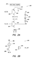
FIG. 2A is a schematic representation of a memory array 200, such as the memory array 104 of FIG. 1. The memory array 200 may include a memory cell 202, a bit line 204, a bit line driver 206, a bit line select 208, a sense amplifier 210, a word line 220, a word line driver 222, a word line select 224, a control circuit 226, and a capacitor 230.
The memory cell 202 may be formed of any of a variety of known or later-developed materials. For example and not by way of limitation, the memory cell 202 may be formed of chalcogenide/PVM or chalcogenide-type materials. The memory cell 202 may be a two-terminal memory cell. The memory cell 202 may include an isolation unit. The isolation unit may include a diode including an anode and a cathode. The anode side may be sensed. The cathode side may be controlled. Alternatively, the anode side may be controlled, and the cathode side may be sensed.
The memory cell 202 may be connected to the bit line 204. The bit line 204 may be coupled to a terminal on the anode side of the memory cell 202. That is, the bit line may be on the sensed side. The bit line 204 may be long relative to the word line 220. The bit line 204 may be connected to the bit line driver 206. The bit line driver 206 may be controlled by the bit line select 208. When the bit line select 208 is enabled, it may connect the bit line 204 to the sense amplifier 210. The bit line driver 206 may be enabled or disabled based on a charge of the capacitor 230.
The memory cell 202 may be connected to the word line 220. The word line 220 may be coupled to a terminal on the cathode side of the memory cell 202. That is, the word line may be on the side that is controlled. The word line 220 may be connected to the word line driver 222. The word line driver 222 may be controlled by the word line select 224. When the word line select 224 is enabled, it may connect the word line 220 to the control circuit 226. The word line 220 may be shorted together with another word line so that word lines are shared.
The sense amplifier 210 may be a write sense amplifier. As will be described further below, the sense amplifier 210 may control programming of the memory cell 202 in conjunction with the control circuit 226.
The control circuit 226 may include a dedicated regulator (e.g., a MUX). The control circuit 226 may control the amount of voltage applied to the word line 220. The control circuit 226 may switch between two voltages.
It should be noted that the word line and the bit line may be switched between more than two voltages, such as from standby voltages to, for example, a first voltage and to a second voltage. Examples of standby voltages are described in U.S. Pat. Nos. 6,822,903 and 6,963,504, both to Scheuerlein and Knall, and both entitled “APPARATUS AND METHOD FOR DISTURB-FREE PROGRAMMING OF PASSIVE ELEMENT MEMORY CELLS,” both of which are incorporated by reference herein in their entirety for all purposes. In these examples, first and second array lines may be driven to selected bias voltages. Then, the first and second array lines may be driven to unselected bias voltages. The timing of when the first and second array lines may be driven to selected bias voltages and when the first and second array lines may be driven to unselected bias voltages may be adjusted relative to one another (i.e., the first array line relative to the second array line), for example, to prevent unintended programming of cells located near target cells in an array. It should be appreciated that in the present disclosure, such standby voltages should not be confused with the first voltage (i.e., as discussed below, the voltage that, when coupled with the voltage applied to the bit line, results in a safe voltage).
The first voltage (e.g., 3 volts) may be high enough that when coupled with voltage applied to the bit line 204 (e.g., 8 volts), may result in a net voltage (e.g., 5 volts) that may be less than a voltage that may program the memory cell 202. That is, the first voltage may result in a safe voltage. The second voltage (e.g., 0 volts) may be low enough that when coupled with voltage applied to the bit line 204 (e.g., 8 volts), may result in a net voltage (e.g., 8 volts) effective to program the memory cell 202. That is, the second voltage may result in a programming voltage.
Alternatively, the control circuit 226 may include a diode connected NMOS device and a bypass path. The diode connected NMOS device may generate the first voltage (i.e., the safe voltage). The bypass path, when selected, may generate the second voltage (resulting in the programming voltage).
The actual value of the first and second voltages may be determined based upon multiple considerations. One consideration may be that the difference between the two voltages should be sufficient to distinguish between programming and not programming. Another consideration may be that the smaller the difference between the two voltages is, the faster the programming of the memory cell 202 may be.
FIG. 2B is a schematic representation of a sense amplifier 250, such as the sense amplifier 210 of FIG. 2A. The sense amplifier 250 may be a write sense amplifier. The sense amplifier 250 may control programming of the memory cell 202 in conjunction with the control circuit 226. The sense amplifier 250 may include a voltage 252, a current limiter 254, a node 256, a pMOS 258, and a voltage reference 260.
The voltage 252 may flow through the current limiter 254, the node 256, and the pMOS 258. The current limit may limit to a predetermined amount (e.g., 1 microamp). The voltage 252 may be compared with the voltage reference 260. Once the memory cell 202 programs, the voltage 252 flowing through the node 256 may fall.
The operation of the memory array 200 is now described with reference to FIGS. 3 and 4, which illustrate, respectively, an exemplary method 300 of programming a memory cell 202, and voltages 400 of a bit line 204 and a word line 220.
In operation 302, the word line 220 may be set to a first voltage 406. For example and not by limitation, the voltage of the word line 220 may be set to 3 volts. The word line select 224 may be enabled thereby connecting the word line 220 through the word line driver 222 to the control circuit 226.
In operation 304, the bit line 204 may be charged from an initial level 402 to a predetermined voltage 404. For example and not by limitation, the bit line 204 may be charged from an initial level of 0 volts to a predetermined voltage of 8 volts. The bit line 204 may be charged from the initial level 402 to the predetermined voltage 404 quickly and without limitation. The bit line select 208 may be enabled thereby connecting the bit line 204 through the bit line driver 206 to the sense amplifier 210.
The first voltage 406 of the word line (e.g., 3 volts) may be high enough that relative to the predetermined voltage 404 of the bit line 204 (e.g., 8 volts), a net voltage difference results (e.g., 5 volts) that may be less than a voltage needed to program the memory cell 202. That is, the first voltage 406 may result in a safe voltage.
In operation 306, the word line 220 may be switched from the first voltage 406 to a second voltage 408. The second voltage (e.g., 0 volts) may be low enough that relative to the predetermined voltage 404 applied to the bit line 204 (e.g., 8 volts), a net voltage difference (e.g., 8 volts) may result that is effective to program the memory cell 202. That is, the second voltage 408 may result in a programming voltage. The control circuit 226 may switch between the first voltage 406 and the second voltage 408.
As noted above, the bit line 204 may be long relative to the word line 220. Thus, the switching of the word line 220 may be faster than if the bit line were switched or otherwise controlled.
The foregoing description discloses only exemplary embodiments of the invention. Modifications of the above-disclosed embodiments of the present invention of which fall within the scope of the invention will be readily apparent to those of ordinary skill in the art.
Accordingly, while the present invention has been disclosed in connection with exemplary embodiments thereof, it should be understood that other embodiments may fall within the spirit and scope of the invention as defined by the following claims.

Claims (20)

The invention claimed is:
1. A method of programming a memory cell having a first terminal coupled to a word line and a second terminal coupled to a bit line, the method comprising:
during a first predetermined time interval, switching the word line from a first standby voltage to a first voltage, and switching the bit line from a second standby voltage to a predetermined voltage; and
during a second predetermined time interval, switching the word line from the first voltage to a second voltage,
wherein:
during the first predetermined time interval, a voltage drop across the first and second terminals is a safe voltage that does not program the memory cell, and
during the second predetermined time interval, a voltage drop across the first and second terminals is a programming voltage that is sufficient to program the memory cell.
2. The method of claim 1, wherein a difference between the safe voltage and the programming voltage maximizes programming speed.
3. The method of claim 1, wherein a difference between the safe voltage and the programming voltage distinguishes between programming and not programming the memory cell.
4. The method of claim 1, wherein the bit line is switched to the predetermined voltage without limiting current.
5. The method of claim 1, wherein the first voltage is higher than the second voltage.
6. The method of claim 1, wherein switching the word line from the first voltage to a second voltage includes a VT drop.
7. Apparatus for programming a memory cell having a first terminal coupled to a word line and a second terminal coupled to a bit line, the apparatus comprising:
a control circuit coupled to the word line; and
a sense amplifier coupled to the bit line;
wherein:
during a first predetermined time interval, the control circuit is adapted to switch the word line from a first standby voltage to a first voltage, the sense amplifier is adapted to charge the bit line from a second standby voltage to a predetermined voltage, and a voltage drop across the first and second terminals is a safe voltage that does not program the memory cell, and
during a second predetermined time interval, the control circuit is adapted to switch the word line from the first voltage to a second voltage, and a voltage drop across the first and second terminals is a programming voltage that is sufficient to program the memory cell.
8. The apparatus of claim 7, wherein the control circuit comprises a MUX or a diode-connected NMOS transistor and a bypass path.
9. The apparatus of claim 7, wherein a difference between the safe voltage and the programming voltage maximizes programming speed.
10. The apparatus of claim 7, wherein a difference between the safe voltage and the programming voltage distinguishes between programming and not programming the memory cell.
11. The apparatus of claim 7, wherein the bit line is switched to the predetermined voltage without limiting current.
12. The apparatus of claim 7, wherein the first voltage is higher than the second voltage.
13. The apparatus of claim 7, wherein switching the word line from the first voltage to a second voltage includes a VT drop.
14. A memory array including a memory cell having a first terminal coupled to a word line and a second terminal coupled to a bit line, the memory array comprising:
a control circuit coupled to the word line; and
a sense amplifier coupled to the bit line;
wherein:
during a first predetermined time interval, the control circuit is adapted to switch the word line from a first standby voltage to a first voltage, the sense amplifier is adapted to charge the bit line from a second standby voltage to a predetermined voltage, and a voltage drop across the first and second terminals is a safe voltage that does not program the memory cell, and
during a second predetermined time interval, the control circuit is adapted to switch the word line from the first voltage to a second voltage, and a voltage drop across the first and second terminals is a programming voltage that is sufficient to program the memory cell.
15. The memory array of claim 14, wherein the control circuit comprises MUX or a diode-connected NMOS transistor and a bypass path.
16. The memory array of claim 14, wherein a difference between the safe voltage and the programming voltage maximizes programming speed.
17. The memory array of claim 14, wherein a difference between the safe voltage and the programming voltage distinguishes between programming and not programming the memory cell.
18. The memory array of claim 14, wherein the bit line is switched to the predetermined voltage without limiting current.
19. The memory array of claim 14, wherein the first voltage is higher than the second voltage.
20. The memory array of claim 14, wherein switching the word line from the first voltage to a second voltage includes a VT drop.
US13/890,622 2009-08-31 2013-05-09 Methods and apparatus for reducing programming time of a memory cell Active US8773898B2 (en)

Priority Applications (2)

Application Number Priority Date Filing Date Title
US13/890,622 US8773898B2 (en) 2009-08-31 2013-05-09 Methods and apparatus for reducing programming time of a memory cell
US14/290,888 US9202539B2 (en) 2009-08-31 2014-05-29 Methods and apparatus for reducing programming time of a memory cell

Applications Claiming Priority (3)

Application Number Priority Date Filing Date Title
US12/551,548 US8125822B2 (en) 2009-08-31 2009-08-31 Reducing programming time of a memory cell
US13/403,454 US8441849B2 (en) 2009-08-31 2012-02-23 Reducing programming time of a memory cell
US13/890,622 US8773898B2 (en) 2009-08-31 2013-05-09 Methods and apparatus for reducing programming time of a memory cell

Related Parent Applications (1)

Application Number Title Priority Date Filing Date
US13/403,454 Continuation US8441849B2 (en) 2009-08-31 2012-02-23 Reducing programming time of a memory cell

Related Child Applications (1)

Application Number Title Priority Date Filing Date
US14/290,888 Continuation US9202539B2 (en) 2009-08-31 2014-05-29 Methods and apparatus for reducing programming time of a memory cell

Publications (2)

Publication Number Publication Date
US20130242681A1 US20130242681A1 (en) 2013-09-19
US8773898B2 true US8773898B2 (en) 2014-07-08

Family

ID=43624699

Family Applications (4)

Application Number Title Priority Date Filing Date
US12/551,548 Expired - Fee Related US8125822B2 (en) 2009-08-31 2009-08-31 Reducing programming time of a memory cell
US13/403,454 Active US8441849B2 (en) 2009-08-31 2012-02-23 Reducing programming time of a memory cell
US13/890,622 Active US8773898B2 (en) 2009-08-31 2013-05-09 Methods and apparatus for reducing programming time of a memory cell
US14/290,888 Expired - Fee Related US9202539B2 (en) 2009-08-31 2014-05-29 Methods and apparatus for reducing programming time of a memory cell

Family Applications Before (2)

Application Number Title Priority Date Filing Date
US12/551,548 Expired - Fee Related US8125822B2 (en) 2009-08-31 2009-08-31 Reducing programming time of a memory cell
US13/403,454 Active US8441849B2 (en) 2009-08-31 2012-02-23 Reducing programming time of a memory cell

Family Applications After (1)

Application Number Title Priority Date Filing Date
US14/290,888 Expired - Fee Related US9202539B2 (en) 2009-08-31 2014-05-29 Methods and apparatus for reducing programming time of a memory cell

Country Status (1)

Country Link
US (4) US8125822B2 (en)

Cited By (1)

* Cited by examiner, † Cited by third party
Publication number Priority date Publication date Assignee Title
US20140269129A1 (en) * 2009-08-31 2014-09-18 Sandisk 3D Llc Methods and apparatus for reducing programming time of a memory cell

Families Citing this family (1)

* Cited by examiner, † Cited by third party
Publication number Priority date Publication date Assignee Title
US8379437B2 (en) 2009-08-31 2013-02-19 Sandisk 3D, Llc Flexible multi-pulse set operation for phase-change memories

Citations (24)

* Cited by examiner, † Cited by third party
Publication number Priority date Publication date Assignee Title
US5737259A (en) 1996-11-22 1998-04-07 United Microelectronics Corporation Method of decoding a diode type read only memory
US5982659A (en) 1996-12-23 1999-11-09 Lsi Logic Corporation Memory cell capable of storing more than two logic states by using different via resistances
US6191972B1 (en) 1999-04-30 2001-02-20 Nec Corporation Magnetic random access memory circuit
US6285582B1 (en) 2000-03-20 2001-09-04 Epitaxial Technologies, Llc Two-dimensional resonant tunneling diode memory system
US6545898B1 (en) 2001-03-21 2003-04-08 Silicon Valley Bank Method and apparatus for writing memory arrays using external source of high programming voltage
US6618295B2 (en) 2001-03-21 2003-09-09 Matrix Semiconductor, Inc. Method and apparatus for biasing selected and unselected array lines when writing a memory array
US6625054B2 (en) 2001-12-28 2003-09-23 Intel Corporation Method and apparatus to program a phase change memory
US6747893B2 (en) 2002-03-14 2004-06-08 Intel Corporation Storing data in non-volatile memory devices
US6822903B2 (en) 2003-03-31 2004-11-23 Matrix Semiconductor, Inc. Apparatus and method for disturb-free programming of passive element memory cells
US20060166455A1 (en) 2005-01-25 2006-07-27 George Gordon Multilevel programming of phase change memory cells
US7283389B2 (en) 2005-12-09 2007-10-16 Macronix International Co., Ltd. Gated diode nonvolatile memory cell array
US7283387B2 (en) 2005-09-08 2007-10-16 Samsung Electronics Co., Ltd. Phase change random access memory device having variable drive voltage circuit
WO2008013619A2 (en) 2006-07-27 2008-01-31 Cswitch Corporation Method and apparatus for programming phase change devices
US7440315B2 (en) 2007-01-09 2008-10-21 Macronix International Co., Ltd. Method, apparatus and computer program product for stepped reset programming process on programmable resistive memory cell
US20090052227A1 (en) 2007-05-11 2009-02-26 Kabushiki Kaisha Toshiba Non-volatile memory device and method for writing data thereto
US7577024B2 (en) 2007-05-25 2009-08-18 Intel Corporation Streaming mode programming in phase change memories
US20090207647A1 (en) 2008-02-14 2009-08-20 Kabushiki Kaisha Toshiba Nonvolatile semiconductor storage device and data writing method therefor
US7813167B2 (en) 2008-03-21 2010-10-12 Micron Technology, Inc. Memory cell
US7869260B2 (en) 2008-06-30 2011-01-11 Kabushiki Kaisha Toshiba Semiconductor storage device
US20110051505A1 (en) 2009-08-31 2011-03-03 Sandisk 3D Llc Reducing programming time of a memory cell
US20110051504A1 (en) 2009-08-31 2011-03-03 Sandisk 3D Llc Creating short program pulses in asymmetric memory arrays
US20110051506A1 (en) 2009-08-31 2011-03-03 Sandisk 3D Llc Flexible multi-pulse set operation for phase-change memories
US7916530B2 (en) 2003-08-07 2011-03-29 Contour Semiconductor, Inc. SCR matrix storage device
US8014201B2 (en) 2008-07-30 2011-09-06 Samsung Electronics Co., Ltd. Nonvolatile memory device extracting parameters and nonvolatile memory system including the same

Family Cites Families (3)

* Cited by examiner, † Cited by third party
Publication number Priority date Publication date Assignee Title
JP4024196B2 (en) * 2003-09-30 2007-12-19 三洋電機株式会社 Ferroelectric memory
JP2005183557A (en) * 2003-12-18 2005-07-07 Canon Inc Semiconductor integrated circuit and its operation method, and ic card having the circuit
US7020026B2 (en) * 2004-05-05 2006-03-28 Sandisk Corporation Bitline governed approach for program control of non-volatile memory

Patent Citations (31)

* Cited by examiner, † Cited by third party
Publication number Priority date Publication date Assignee Title
US5737259A (en) 1996-11-22 1998-04-07 United Microelectronics Corporation Method of decoding a diode type read only memory
US5982659A (en) 1996-12-23 1999-11-09 Lsi Logic Corporation Memory cell capable of storing more than two logic states by using different via resistances
US6191972B1 (en) 1999-04-30 2001-02-20 Nec Corporation Magnetic random access memory circuit
US6285582B1 (en) 2000-03-20 2001-09-04 Epitaxial Technologies, Llc Two-dimensional resonant tunneling diode memory system
US6545898B1 (en) 2001-03-21 2003-04-08 Silicon Valley Bank Method and apparatus for writing memory arrays using external source of high programming voltage
US6618295B2 (en) 2001-03-21 2003-09-09 Matrix Semiconductor, Inc. Method and apparatus for biasing selected and unselected array lines when writing a memory array
US6625054B2 (en) 2001-12-28 2003-09-23 Intel Corporation Method and apparatus to program a phase change memory
US6747893B2 (en) 2002-03-14 2004-06-08 Intel Corporation Storing data in non-volatile memory devices
US6822903B2 (en) 2003-03-31 2004-11-23 Matrix Semiconductor, Inc. Apparatus and method for disturb-free programming of passive element memory cells
US6963504B2 (en) 2003-03-31 2005-11-08 Matrix Semiconductor, Inc. Apparatus and method for disturb-free programming of passive element memory cells
US7916530B2 (en) 2003-08-07 2011-03-29 Contour Semiconductor, Inc. SCR matrix storage device
US20060166455A1 (en) 2005-01-25 2006-07-27 George Gordon Multilevel programming of phase change memory cells
US7283387B2 (en) 2005-09-08 2007-10-16 Samsung Electronics Co., Ltd. Phase change random access memory device having variable drive voltage circuit
US7283389B2 (en) 2005-12-09 2007-10-16 Macronix International Co., Ltd. Gated diode nonvolatile memory cell array
WO2008013619A2 (en) 2006-07-27 2008-01-31 Cswitch Corporation Method and apparatus for programming phase change devices
US7440315B2 (en) 2007-01-09 2008-10-21 Macronix International Co., Ltd. Method, apparatus and computer program product for stepped reset programming process on programmable resistive memory cell
US20090052227A1 (en) 2007-05-11 2009-02-26 Kabushiki Kaisha Toshiba Non-volatile memory device and method for writing data thereto
US7889537B2 (en) 2007-05-11 2011-02-15 Kabushiki Kaisha Toshiba Non-volatile memory device and method for writing data thereto
US7577024B2 (en) 2007-05-25 2009-08-18 Intel Corporation Streaming mode programming in phase change memories
US20090207647A1 (en) 2008-02-14 2009-08-20 Kabushiki Kaisha Toshiba Nonvolatile semiconductor storage device and data writing method therefor
US7813167B2 (en) 2008-03-21 2010-10-12 Micron Technology, Inc. Memory cell
US7869260B2 (en) 2008-06-30 2011-01-11 Kabushiki Kaisha Toshiba Semiconductor storage device
US8014201B2 (en) 2008-07-30 2011-09-06 Samsung Electronics Co., Ltd. Nonvolatile memory device extracting parameters and nonvolatile memory system including the same
US20110051506A1 (en) 2009-08-31 2011-03-03 Sandisk 3D Llc Flexible multi-pulse set operation for phase-change memories
US20110051504A1 (en) 2009-08-31 2011-03-03 Sandisk 3D Llc Creating short program pulses in asymmetric memory arrays
US20110051505A1 (en) 2009-08-31 2011-03-03 Sandisk 3D Llc Reducing programming time of a memory cell
US8040721B2 (en) * 2009-08-31 2011-10-18 Sandisk 3D Llc Creating short program pulses in asymmetric memory arrays
US8125822B2 (en) * 2009-08-31 2012-02-28 Sandisk 3D Llc Reducing programming time of a memory cell
US20120155163A1 (en) 2009-08-31 2012-06-21 Tyler Thorp Reducing programming time of a memory cell
US8441849B2 (en) * 2009-08-31 2013-05-14 Sandisk 3D Llc Reducing programming time of a memory cell
US20130148421A1 (en) 2009-08-31 2013-06-13 Sandisk 3D Llc Methods of programming two terminal memory cells

Non-Patent Citations (22)

* Cited by examiner, † Cited by third party
Title
Apr. 20, 2012 Response to Jan. 20, 2012 Office Action of related U.S. Appl. No. 12/551,553.
Apr. 5, 2011 Reply to Jan. 6, 2011 Office Action of related U.S. Appl. No. 12/551,548.
Aug. 16, 2012 RCE and Response to May 17, 2012 Final Office Action of related U.S. Appl. No. 12/551,553.
Dec. 19, 2011 Reply to Nov. 25, 2011 Restriction Requirement of related U.S. Appl. No. 12/551,553.
Dec. 19, 2012 Terminal Disclaimers and Response to Sep. 21, 2012 Office Action of related U.S. Appl. No. 13/403,454.
Final Office Action of related U.S. Appl. No. 12/551,553 mailed May 17, 2012.
Hanzawa et al., "A 512kB Embedded Phase Change Memory with 416kB/s Write Throughput at 100 muA Cell Write Current", 2007 IEEE International Solid-State Circuits Conference, Session 26/Non-Volatile Memories/26.2, pp. 474, 475 and 616.
Hanzawa et al., "A 512kB Embedded Phase Change Memory with 416kB/s Write Throughput at 100 μA Cell Write Current", 2007 IEEE International Solid-State Circuits Conference, Session 26/Non-Volatile Memories/26.2, pp. 474, 475 and 616.
International Search Report and Written Opinion of related International Application No. PCT/US2010/045684 Jan. 31, 2011.
Lee et al., "A 90nm 1.8V 512Mb Diode-Switch PRAM with 266MB/s Read Throughput", Feb. 14, 2007; 2007 IEEE International Solid-State Circuits Conference, Session 26/Non-Volatile Memories/26.1, pp. 472, 473 and 616.
Notice of Allowance in related U.S. Appl. No. 13/403,454 mailed Jan. 23, 2013.
Notice of Allowance of related U.S. Appl. No. 12/551,548 mailed May 23, 2011.
Notice of Allowance of related U.S. Appl. No. 12/551,548 mailed Oct. 26, 2011.
Notice of Allowance of related U.S. Appl. No. 12/551,553 mailed Oct. 12, 2012.
Notice of Allowance of related U.S. Appl. No. 13/765,394 mailed Jul. 10, 2013.
Notice of Allowance of U.S. Appl. No. 12/551,546 mailed Apr. 15, 2011.
Notice of Allowance of U.S. Appl. No. 12/551,546 mailed Jun. 21, 2011.
Office Action of related U.S. Appl. No. 12/551,553 Jan. 20, 2012.
Office Action of related U.S. Appl. No. 13/403,454 mailed Sep. 21, 2012.
Office Action of U.S. Appl. No. 12/551,548 mailed Jan. 6, 2011.
Partial International Search of related International Application No. PCT/US2010/045684 Annex to invitation to pay additional fees dated Nov. 18, 2010.
Restriction Requirement of related U.S. Appl. No. 12/551,553 mailed Nov. 25, 2011.

Cited By (2)

* Cited by examiner, † Cited by third party
Publication number Priority date Publication date Assignee Title
US20140269129A1 (en) * 2009-08-31 2014-09-18 Sandisk 3D Llc Methods and apparatus for reducing programming time of a memory cell
US9202539B2 (en) * 2009-08-31 2015-12-01 Sandisk 3D Llc Methods and apparatus for reducing programming time of a memory cell

Also Published As

Publication number Publication date
US20130242681A1 (en) 2013-09-19
US8441849B2 (en) 2013-05-14
US20110051505A1 (en) 2011-03-03
US20120155163A1 (en) 2012-06-21
US8125822B2 (en) 2012-02-28
US20140269129A1 (en) 2014-09-18
US9202539B2 (en) 2015-12-01

Similar Documents

Publication Publication Date Title
KR102571192B1 (en) Sense amplifier, non-volatile memory apparatus and system including the same
US8040721B2 (en) Creating short program pulses in asymmetric memory arrays
US7391638B2 (en) Memory device for protecting memory cells during programming
US7391644B2 (en) Phase-changeable memory device and read method thereof
US8243542B2 (en) Resistance variable memory devices and read methods thereof
US7894236B2 (en) Nonvolatile memory devices that utilize read/write merge circuits
US7668007B2 (en) Memory system including a resistance variable memory device
US7589989B2 (en) Method for protecting memory cells during programming
US8526226B2 (en) Current control apparatus and phase change memory having the same
US9202539B2 (en) Methods and apparatus for reducing programming time of a memory cell
JP2001014877A (en) Voltage generating circuit and semiconductor storage provided with it
US8310874B2 (en) Non-volatile memory device
US6351180B1 (en) Clamp circuit with fuse options
US8565015B2 (en) Methods of programming two terminal memory cells
KR20180045690A (en) Sense amplifier, non-volatile memory apparatus and system including the same
US9019783B2 (en) Semiconductor memory device including write driver and method of controlling the same
US7321505B2 (en) Nonvolatile memory utilizing asymmetric characteristics of hot-carrier effect
CN111383685B (en) Variable resistive memory device and method for performing memory operations
US6873554B1 (en) Semiconductor memory device
WO2008051835A1 (en) Memory device and method for protecting memory cells during programming
US10748611B2 (en) Resistive random access memory device and method for performing memory operations

Legal Events

Date Code Title Description
STCF Information on status: patent grant

Free format text: PATENTED CASE

AS Assignment

Owner name: SANDISK TECHNOLOGIES INC., TEXAS

Free format text: ASSIGNMENT OF ASSIGNORS INTEREST;ASSIGNOR:SANDISK 3D LLC.;REEL/FRAME:038300/0665

Effective date: 20160324

AS Assignment

Owner name: SANDISK TECHNOLOGIES INC., TEXAS

Free format text: CORRECTIVE ASSIGNMENT TO CORRECT THE INCORRECT LISTED PATENT NUMBER 8853569 TO THE CORRECT PATENT NUMBER 8883569 PREVIOUSLY RECORDED ON REEL 038300 FRAME 0665. ASSIGNOR(S) HEREBY CONFIRMS THE ASSIGNMENT;ASSIGNOR:SANDISK 3D LLC;REEL/FRAME:038520/0552

Effective date: 20160324

AS Assignment

Owner name: SANDISK TECHNOLOGIES LLC, TEXAS

Free format text: CHANGE OF NAME;ASSIGNOR:SANDISK TECHNOLOGIES INC;REEL/FRAME:038807/0898

Effective date: 20160516

MAFP Maintenance fee payment

Free format text: PAYMENT OF MAINTENANCE FEE, 4TH YEAR, LARGE ENTITY (ORIGINAL EVENT CODE: M1551)

Year of fee payment: 4

MAFP Maintenance fee payment

Free format text: PAYMENT OF MAINTENANCE FEE, 8TH YEAR, LARGE ENTITY (ORIGINAL EVENT CODE: M1552); ENTITY STATUS OF PATENT OWNER: LARGE ENTITY

Year of fee payment: 8