US8773083B2 - Detection of insufficient current sourcing capability of supplied power - Google Patents
Detection of insufficient current sourcing capability of supplied power Download PDFInfo
- Publication number
- US8773083B2 US8773083B2 US13/353,470 US201213353470A US8773083B2 US 8773083 B2 US8773083 B2 US 8773083B2 US 201213353470 A US201213353470 A US 201213353470A US 8773083 B2 US8773083 B2 US 8773083B2
- Authority
- US
- United States
- Prior art keywords
- current
- power source
- insufficient
- response
- selectively
- Prior art date
- Legal status (The legal status is an assumption and is not a legal conclusion. Google has not performed a legal analysis and makes no representation as to the accuracy of the status listed.)
- Active, expires
Links
Images


Classifications
-
- H—ELECTRICITY
- H02—GENERATION; CONVERSION OR DISTRIBUTION OF ELECTRIC POWER
- H02J—CIRCUIT ARRANGEMENTS OR SYSTEMS FOR SUPPLYING OR DISTRIBUTING ELECTRIC POWER; SYSTEMS FOR STORING ELECTRIC ENERGY
- H02J1/00—Circuit arrangements for dc mains or dc distribution networks
- H02J1/14—Balancing the load in a network
-
- G—PHYSICS
- G01—MEASURING; TESTING
- G01R—MEASURING ELECTRIC VARIABLES; MEASURING MAGNETIC VARIABLES
- G01R31/00—Arrangements for testing electric properties; Arrangements for locating electric faults; Arrangements for electrical testing characterised by what is being tested not provided for elsewhere
- G01R31/36—Arrangements for testing, measuring or monitoring the electrical condition of accumulators or electric batteries, e.g. capacity or state of charge [SoC]
- G01R31/382—Arrangements for monitoring battery or accumulator variables, e.g. SoC
Definitions
- a useful feature for battery-powered products is a “low-battery alert,” an alert to notify the user in time to replace the battery before it is completely discharged and service is interrupted.
- the voltage supplied to the product may vary under varying load conditions. To ensure that an undetected under-voltage condition does not occur, substantially-constant monitoring of the voltage supplied by the source is therefore required.
- Existing insufficient-supply detectors typically require a dedicated analog comparator and the generation of a reference voltage to use in the comparison process. These circuits consume additional power, and so in many products are often rarely enabled. Undetected insufficient-supply conditions, therefore, can occur, leading to undesired product behavior.
- FIGS. 1(A) , 1 (B), and 1 (C) illustrate examples of current multipliers, in accordance with various representative embodiments.
- FIG. 2 is a block diagram of an example voltage regulator, in accordance with various representative embodiments.
- FIG. 3 is a block diagram of an example insufficient-supply detector, in accordance with various representative embodiments.
- FIGS. 4(A) and 4(B) illustrate examples of operation of an insufficient-supplied power detector, in accordance with various representative embodiments.
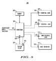
- FIG. 5 is a functional block diagram of in which an insufficient-supply indicator may be used to control various loads of a device, in accordance with various representative embodiments.
- FIG. 6 is a flowchart that illustrates a method of detection, in accordance with various representative embodiments.
- the various methods, apparatus, and devices described herein provide for the detection of insufficient supplied power provided to a device, and also for reaction by the device to the detection of insufficient supplied power.
- various methodologies for determining the adequacy of the current sourcing capability of a power source including: dynamically detecting a current sourcing capability of the power source; generating an insufficient-supply indication, that the current sourcing capability of the power source has fallen below a current threshold of a device supplied power by the power source, in response to an overflow condition of a digital counter of the device, the overflow condition caused by a current multiplier of the device to which the digital counter is coupled being unable to achieve a threshold voltage within N count cycles of a clock signal used to clock the digital counter; and in response to the insufficient-supply indication, a control element of the device controlling the device to have a compensatory response.
- an apparatus that determines the adequacy of the current sourcing capability of a power source that supplies power to a device.
- the apparatus has a current multiplier of the device, operable as a voltage regulator, that is coupled to the power source, receives a clock signal, and generates a control signal; and a digital counter, clocked by the clock signal and reset by the control signal, that generates an overflow output in response to an overflow condition of the digital counter that indicates that the current sourcing capability of the power source has fallen below a current threshold of the device.
- the digital counter generates the overflow condition of the digital counter in response to the current multiplier of the device being unable to achieve a threshold voltage within N count cycles of the clock signal.
- the current multiplier resides on the device supplied power by the power source and the digital counter may or may not also reside on the device.
- a device that is provided power by a power source, with the device having a detection element operable to dynamically detect a current sourcing capability of the power source and generate an insufficient-supply indication when the current sourcing capability of the power source has fallen below a current threshold of the device; and a control element operable to monitor the insufficient-supply indication and, in response to generation of the insufficient-supply indication by the detection element, the control element controls the device to have a compensatory response to the insufficient-supply indication.
- the detection element has a current multiplier, operable as a voltage regulator and having a control signal, that is coupled to the power source and receives a clock signal; and a digital counter, clocked by the clock signal and reset by the control signal, that generates an overflow output as the insufficient-supply indication in response to an overflow condition of the digital counter.
- a warning or alert indication that the power source cannot adequately power the product has many uses.
- the most familiar may be the “low battery” alert in battery-powered products, used to notify the user in time to replace the battery before it is completely discharged and service is interrupted.
- Another use for such an alert is load shedding, or the disconnection of non-essential loads to preserve the function of essential loads.
- Loads often shed in portable products include display backlights, audible user feedback, and non-critical wireless transmission and reception.
- digital products may have their supply voltage and/or clock speeds lowered, to lower the power consumption of the remaining circuits, at the cost of reduced performance.
- Load shedding may be extended to the point of actually performing an orderly product shutdown.
- Load shedding like the “low battery” alert, may be done under microprocessor control in response to the insufficient-supply detection; in this way the response may be tailored, via software, to the state of the product at the instant the detection of an insufficient power supply is made.
- a third use for insufficient-supply detection is the reduction of peak currents by the rescheduling of product actions, spreading them so that they do not occur at the same time. For example, in a user interface a backlight flash and a user-audible alert can be separated in time so that their currents may be separated in time.
- Products supplied by variable sources often employ switching converters to convert the voltage presented by a source to a voltage needed by a load. Due to their small physical size and suitability for semiconductor integration, current multipliers, also known as capacitive switching converters and capacitive voltage converters, are well suited for this application.
- the current multiplier generates an output current that is a function of the difference between its input voltage and output voltage. A description of its operation follows.
- FIG. 1(A) An exemplary current multiplier 101 is shown in FIG. 1(A) .
- source 102 is coupled to switch 104 .
- Capacitor 106 is coupled to switches 104 , 108 , 110 , and 112 ; capacitor 114 is coupled to switches 108 and 110 , load 116 , and output 118 .
- Switches 104 and 108 are controlled by clock signal ⁇ 1 ;
- Switches 110 and 112 are controlled by clock signal ⁇ 2 .
- Clock signals ⁇ 1 and ⁇ 2 are non-overlapping, meaning that the two signals are never high at the same instant in time, and are commonly generated from a single clock source.
- the current drain multiplication can be analyzed by neglecting the current into load 116 and analyzing the charge transfer. Assume that capacitor 114 is a much higher value than capacitor 106 , such that the voltage on capacitor 114 does not change significantly as capacitor 106 charges and discharges. Further, assume that the circuit reaches a steady-state condition before the next clock transition.
- phase 2 i.e., while clock signal ⁇ 2 is high
- FIG. 1(C) capacitor 106 discharges into capacitor 114 .
- the amount of current from source 102 is
- Current multipliers are often placed in a feedback arrangement, forming a voltage regulator 200 as shown in FIG. 2 .
- current multiplier 201 is coupled to supply 216 via input 202 .
- Current multiplier 201 may be, e.g., current multiplier 101 of FIG. 1 .
- Output 218 of current multiplier 201 is coupled to the load, and also to comparator 204 .
- Comparator 204 is coupled to voltage threshold v th via threshold input 208 , and hysteresis v h via hysteresis input 210 .
- Output 212 of comparator 204 is coupled to clock generator 206 .
- Clock generator 206 is coupled to switching clock source 214 , having frequency f c , and generates non-overlapping clock signals ⁇ 1 and ⁇ 2 coupled to current multiplier 201 .
- the control structure for multiplier 201 is comparator 204 , having a threshold voltage 208 , v th , and a hysteresis voltage 210 , v h , and clock generator 206 .
- comparator output 212 is high, clock generator 206 is enabled, producing clock signals ⁇ 1 and ⁇ 2 .
- Multiplier 201 then conducts, and the voltage at its output 218 rises until the upper threshold of comparator 204 , v th +v h , is reached. At that point the comparator output 212 switches low, and clock generator 206 is disabled, stopping clock signals ⁇ 1 and ⁇ 2 .
- Multiplier 201 then stops conducting and the voltage at its output 218 drops as the load current drains C load of multiplier 201 (e.g., capacitor 114 inside multiplier 101 ).
- C load of multiplier 201 e.g., capacitor 114 inside multiplier 101 .
- comparator output 212 switches high, and the cycle repeats.
- the rate ( ⁇ v/ ⁇ t) at which the voltage at multiplier output 218 increases during the conduction portion of the cycle is proportional to the difference between the maximum current-sourcing capability I max of the multiplier and the actual load current I load . This can be described by
- I max is determined by the specific implementation details of voltage regulator 200 —principally the values of the capacitors in multiplier 201 and the frequency of switching clock source 214 .
- the multiplier can source no more than twice I cap .
- I cap is reduced, due to a reduction of the source voltage, increase in the source internal impedance, or other cause, a point is reached at which I max becomes limited by I cap , rather than voltage regulator 200 . As I cap is reduced beyond this point, I max is also reduced.
- multiplier 201 and comparator 204 are regulated by the switching clock source 214 and its frequency f c .
- the rate of voltage increase at multiplier output 218 when multiplier 201 is conducting can be expressed as the number of clock cycles N required for the voltage to rise by an amount equal to the hysteresis voltage v h :
- a limit on the number of cycles (N) can be set by setting a minimum value of I max ⁇ I load based on some fraction (x) of the minimum designed value of I max .
- the maximum number of cycles N max can be expressed
- N max v h ⁇ f c ⁇ C load xI max .
- N max v h ⁇ f c ⁇ C load 2 ⁇ x ⁇ ⁇ I cap ,
- an apparatus that determines the adequacy of the current sourcing capability of a power source that supplies power to a device, has a current multiplier of the device, operable as a voltage regulator, that is coupled to the power source, receives a clock signal, and generates a control signal; and a digital counter, clocked by the clock signal and reset by the control signal, that generates an overflow output in response to an overflow condition of the digital counter that indicates that the current sourcing capability of the power source has fallen below a current threshold of the device.
- the digital counter generates the overflow condition of the digital counter in response to the current multiplier of the device being unable to achieve a threshold voltage within N count cycles of the clock signal described below.
- Operation of the apparatus may be embodied within a device being supplied power, in which case both the current multiplier and the digital counter reside on the device, or the digital counter of the apparatus may not reside on the device.
- a device embodying the detection capabilities described herein may be considered to have a detection element operable to dynamically detect a current sourcing capability of the power source and to generate an insufficient-supply indication when the current sourcing capability of the power source has fallen below a current threshold of the device; and a control element operable to monitor the insufficient-supply indication and, in response to generation of the insufficient-supply indication by the detection element, to control the device to have a compensatory response to the insufficient-supply indication.
- the detection element of the device has a current multiplier, operable as a voltage regulator and having a control signal, that is coupled to the power source and receives a clock signal; and a digital counter, clocked by the clock signal and reset by the control signal, that generates an overflow output as the insufficient-supply indication in response to an overflow condition of the digital counter.
- the compensatory response may be an alert indication, such as a low-battery indication, generated by the device under control of the control element, that the current sourcing capability of the power source has fallen below the current threshold of the device.
- the compensatory response may be the control element selectively reducing load current drawn by the device. Load shedding may be accomplished by the control element selectively shutting down operation of one or more load elements of the device that draw current when operational, or even an orderly shut-down of the device itself. Reducing load current drawn by the device may further be accomplished by the control element selectively lowering power consumption of the device, such as by selectively reducing a supply voltage of the device or a clock speed of one or more clocks of the device. Moreover, selectively scheduling the occurrence in time of one or more functions of the device by the control element may be performed to reduce load current drawn by the device.
- current multiplier 301 is coupled to supply 316 via input 302 .
- Current multiplier 301 may be, e.g., current multiplier 101 of FIG. 1 .
- Output 318 of current multiplier 301 is coupled to the load, and also to comparator 304 .
- Comparator 304 is coupled to voltage threshold v th via threshold input 308 , and hysteresis v h via hysteresis input 310 .
- Output 312 of comparator 304 is coupled to clock generator 306 and to resetx input 320 of counter 324 .
- Clock generator 306 is coupled to switching clock source 314 , having frequency f c , and generates non-overlapping clock signals ⁇ 1 and ⁇ 2 coupled to current multiplier 301 .
- Counter 324 is coupled to switching clock source 314 , and has an output 322 representing an insufficient-supply indicator.
- Couplings between blocks in FIG. 3 may be wireless.
- clock generator 306 and counter 324 need not reside on the same device as current multiplier 301 .
- clock generator 306 and counter 324 may reside on a laptop computer, while current multiplier 301 may reside on a docking station coupled to the laptop.
- N max calculations Two sample N max calculations are shown in Table 1, for exemplary regulators having different values of I max .
- the coefficient x is arbitrarily picked to be 0.1. In both cases the number of bits in the counter is reasonable, and suitable for integration.
- a simple ripple counter is sufficient, since such counters have low power dissipation and the counter values N count that produce an overflow condition in counter 316 can approximate N max with sufficient accuracy.
- Regulator 1 Regulator 2 units v h 0.08 0.08 volts f c 3.20E+04 3.20E+07 Hz C load 2.20E ⁇ 06 2.20E ⁇ 06 F x 0.1 0.1 I max 1.00E ⁇ 06 6.00E ⁇ 03 A Minimum I cap required 500E ⁇ 09 3.00E ⁇ 03 A N max 5.63E+04 9.39E+03 N count , the lowest power of 65536 16384 2 value greater than N max number of bits in counter 16 14 bits
- curve 402 shows the operation of a regulator when the source current is unrestricted.
- the multiplier conducts and the regulator output voltage rises rapidly to v th +v h , and then turns off. The voltage then gradually decreases as current is drawn from Capacitor 114 in the current multiplier. When this voltage reaches v th , the multiplier conducts again and the cycle is repeated.
- Curve 404 shows the case in which I cap is low, limiting the current available to the product. In this case, however, because the current from the source is limited, the voltage step height is smaller, and as a result more clock cycles are needed to reach v th +v h .
- Counter 324 counts these clock cycles; when it overflows the determination of an insufficient supply is made. Overflow output 322 of counter 324 thereby operates as an insufficient-supply indicator.
- processor 502 is coupled to the insufficient-supply indicator (e.g., overflow output 322 of counter 324 in FIG. 3 ) at input 514 .
- Processor 502 is also coupled to memory 504 , essential load 506 via enable signal 516 , essential load 508 via enable signal 518 , non-essential load 510 via enable signal 520 , user interface 512 via port 522 , and system clock 524 via control signal 526 and clock signal 528 .
- Couplings between blocks in FIG. 5 may be wireless.
- processor 502 may reside on the device, or may not.
- essential loads 506 and 508 may be, for example, a Global Positioning System (GPS) receiver and a cellular telephone transceiver, respectively.
- Non-essential load 510 may be, for example, an audio amplifier for speakerphone use.
- processor 502 controls essential loads 506 and 508 , non-essential load 510 , and user interface 512 as instructed by software instructions stored in memory 504 .
- the processor may monitor the insufficient-supply indicator at input 514 by polling input 514 , by considering input 514 to be an interrupt, by storing the value of input 514 in a register or memory for later evaluation, or by any other means known in the art.
- processor 502 executes the instructions for this event stored in memory 504 .
- Processor 502 may, for example, activate its user interface, and send a warning (via a visual display, audible tone, or other means) to the user.
- Port 522 on user interface 512 may be a two-way port, enabling the user to reply to the warning by instructing processor 502 on desired current-reduction steps (e.g., by turning off or dimming a display backlight).
- Processor 502 also may, for example, disable non-essential load 510 via enable input 520 , thereby reducing the load current of the product when essential loads 506 and 508 are enabled (load shedding). This would, for example, disable speakerphone use, while still maintaining GPS and conventional telephone capability.
- Processor 502 also may, for example, control system clock 524 via control signal 526 so that the frequency of clock signal 528 , or the frequency of the clock of other product components (not shown in FIG. 5 ), is reduced, thereby reducing the product load current. Moreover, processor 502 may selectively reduce a supply voltage of the device in order to reduce product load current.
- Processor 502 also may, for example, stagger the operation of essential loads 506 and 508 , so that the two are never active simultaneously and the peak load current of the product reduced. In the cellular telephone example, this would stagger the operation of the GPS receiver and the cellular telephone transceiver.
- processor 502 and memory 504 are not the object of load-reduction efforts, however (e.g., by reducing the frequency of clock signal 528 ), they need not be supplied by the same power source as that coupled to the insufficient-supply indicator.
- memory 504 may be any suitable memory technology such as a random access memory (RAM), Read Only Memory (ROM), Flash memory, Electrically Erasable Programmable Read Only Memory (EEPROM), mass storage such as a hard disc drive, floppy disc drive, optical disc drive or may accommodate other electronic storage media, and non-volatile memory (NVM).
- RAM random access memory
- ROM Read Only Memory
- EEPROM Electrically Erasable Programmable Read Only Memory
- mass storage such as a hard disc drive, floppy disc drive, optical disc drive or may accommodate other electronic storage media
- NVM non-volatile memory
- the memory may be active memory or may permanently reside in ROM, EEPROM or Flash memory, for example.
- Processor 502 encompasses a processor, controller, microcontroller unit (MCU), microprocessor, and other suitable control elements. It will be appreciated that embodiments of the invention described herein may be comprised of one or more conventional processors and unique stored program instructions that control the one or more processors to implement, in conjunction with certain non-processor circuits, some, most, or all of the functions described herein.
- the non-processor circuits may include, but are not limited to, a receiver, a transmitter, a radio, signal drivers, clock circuits, power source circuits, and user input devices. As such, these functions may be interpreted as a method to perform functions in accordance with certain embodiments consistent with the present invention.
- ROM Read Only Memory
- RAM Random Access Memory
- EEPROM Electrically Erasable Programmable Read Only Memory
- NVM non-volatile memory
- mass storage such as a hard disc drive, floppy disc drive, optical disc drive; optical storage elements, magnetic storage elements, magneto-optical storage elements, flash memory, core memory and/or other equivalent storage technologies without departing from the present invention.
- Such alternative storage devices should be considered equivalents.
- flowchart 600 illustrates a method of detecting an inadequate current sourcing capability of a power source.
- a current sourcing capability of the power source is dynamically detected. Dynamic detection of the current sourcing capability may include monitoring an overflow output of the digital counter of the device, the insufficient-supply indication, and may be performed periodically or near-continuously to provide information concerning the adequacy of the power source as needed.
- an insufficient-supply indication that the current sourcing capability of the power source has fallen below a current threshold of a device supplied power by the power source, is generated.
- the overflow condition is caused by a current multiplier of the device to which the digital counter is coupled being unable to achieve a threshold voltage within N count cycles of a clock signal used to clock the digital counter.
- a control element of the device controls the device to have a compensatory response.
- a compensatory response by the device may be generation of an alert indication, such as a low-battery alert, or it may be action taken, under processor control, to reduce the current load drawn by the device.
- Selectively reducing the current load of the device may include one or more of selectively shutting down operation of one or more load elements of the device, shutting down the device itself, lowering power consumption utilized by the device (e.g. reducing a supply voltage or a clock speed of the device), and selectively scheduling when functions performed by device occur.
Abstract
Description
q 1 =∫i·dt=∫C·dv,
where C is the capacitance of
q=q 1 +q 2=2C∫dv.
where T is the period of clock signals φ1 and φ2. Recognizing that iload, the current into
So, the ideal performance is 2× current enhancement.
Note that efficiency is minimized when vS−vL is large, and is maximized when vL/vS=1. However, load current approaches zero as vL/vS=1.
where Cload is the capacitance of
| TABLE 1 |
| Calculated values for Nmax and counter size for |
| two regulator designs, per an exemplary embodiment. |
| Regulator 1 | |
units | ||
| vh | 0.08 | 0.08 | volts |
| fc | 3.20E+04 | 3.20E+07 | Hz |
| Cload | 2.20E−06 | 2.20E−06 | F |
| x | 0.1 | 0.1 | |
| Imax | 1.00E−06 | 6.00E−03 | A |
| Minimum Icap required | 500E−09 | 3.00E−03 | A |
| Nmax | 5.63E+04 | 9.39E+03 | |
| Ncount, the lowest power of | 65536 | 16384 | |
| 2 value greater than Nmax | |||
| number of bits in counter | 16 | 14 | bits |
Claims (24)
Priority Applications (3)
| Application Number | Priority Date | Filing Date | Title |
|---|---|---|---|
| US13/353,470 US8773083B2 (en) | 2011-01-24 | 2012-01-19 | Detection of insufficient current sourcing capability of supplied power |
| US13/556,615 US9124131B2 (en) | 2011-01-24 | 2012-07-24 | Dynamic control of the power sourcing capability of a power source |
| US14/839,144 US10007286B2 (en) | 2011-01-24 | 2015-08-28 | Switching regulator overload detector |
Applications Claiming Priority (2)
| Application Number | Priority Date | Filing Date | Title |
|---|---|---|---|
| US201161435509P | 2011-01-24 | 2011-01-24 | |
| US13/353,470 US8773083B2 (en) | 2011-01-24 | 2012-01-19 | Detection of insufficient current sourcing capability of supplied power |
Related Child Applications (1)
| Application Number | Title | Priority Date | Filing Date |
|---|---|---|---|
| US13/556,615 Continuation-In-Part US9124131B2 (en) | 2011-01-24 | 2012-07-24 | Dynamic control of the power sourcing capability of a power source |
Publications (2)
| Publication Number | Publication Date |
|---|---|
| US20120187925A1 US20120187925A1 (en) | 2012-07-26 |
| US8773083B2 true US8773083B2 (en) | 2014-07-08 |
Family
ID=46543708
Family Applications (1)
| Application Number | Title | Priority Date | Filing Date |
|---|---|---|---|
| US13/353,470 Active 2032-02-15 US8773083B2 (en) | 2011-01-24 | 2012-01-19 | Detection of insufficient current sourcing capability of supplied power |
Country Status (2)
| Country | Link |
|---|---|
| US (1) | US8773083B2 (en) |
| WO (1) | WO2012102933A2 (en) |
Cited By (2)
| Publication number | Priority date | Publication date | Assignee | Title |
|---|---|---|---|---|
| WO2018063450A1 (en) * | 2016-09-30 | 2018-04-05 | Cypress Semiconductor Corporation | Low quiescent current dc-to-dc converter |
| US10007286B2 (en) | 2011-01-24 | 2018-06-26 | Sunrise Micro Devices, Inc. | Switching regulator overload detector |
Families Citing this family (2)
| Publication number | Priority date | Publication date | Assignee | Title |
|---|---|---|---|---|
| US8738944B2 (en) * | 2011-11-16 | 2014-05-27 | Cisco Technology, Inc. | Energy-based feedback for transmission reception in a communication network |
| US9347998B2 (en) * | 2013-04-17 | 2016-05-24 | Allegro Microsystems, Llc | System and method for measuring battery voltage |
Citations (26)
| Publication number | Priority date | Publication date | Assignee | Title |
|---|---|---|---|---|
| US5327071A (en) * | 1991-11-05 | 1994-07-05 | The United States Of America As Represented By The Administrator Of The National Aeronautics & Space Administration | Microprocessor control of multiple peak power tracking DC/DC converters for use with solar cell arrays |
| US6054861A (en) | 1994-11-11 | 2000-04-25 | Fujitsu Limited | Apparatus for monitoring power of battery to supply electric power to load |
| US6160490A (en) * | 1998-02-02 | 2000-12-12 | Motorola | Apparatus for improving the battery life of a selective call receiver |
| US6285164B1 (en) | 1998-03-31 | 2001-09-04 | Hitachi, Ltd. | Means for detecting the integrated value of current flow, a means for detecting the value of current flow and a battery pack employing those means |
| JP2002093465A (en) | 2000-09-18 | 2002-03-29 | Tokyo Gas Co Ltd | Battery life estimating device for gas meter |
| US6384579B2 (en) | 2000-06-27 | 2002-05-07 | Origin Electric Company, Limited | Capacitor charging method and charging apparatus |
| US20030169020A1 (en) | 2002-03-05 | 2003-09-11 | Dialog Semiconductor Gmbh | Battery charge monitor |
| US20030221133A1 (en) | 2002-05-24 | 2003-11-27 | Nguyen Don J. | Providing overload protection in battery operation |
| US20040046527A1 (en) | 2002-09-05 | 2004-03-11 | Vandersluis Donald | Apparatus and method for charging and discharging a capacitor to a predetermined setpoint |
| US20040164711A1 (en) | 2003-02-25 | 2004-08-26 | Isao Hayashi | Battery charger and method therefor |
| KR20040076535A (en) | 2003-02-26 | 2004-09-01 | 에스케이텔레텍주식회사 | Method for delaying discharge of battery loaded in mobile phone |
| US6897673B2 (en) | 2003-03-19 | 2005-05-24 | Lsi Logic Corporation | Method and integrated circuit for capacitor measurement with digital readout |
| US7112943B2 (en) | 2002-06-20 | 2006-09-26 | O2Micro International Limited | Enabling circuit for avoiding negative voltage transients |
| US20070103134A1 (en) * | 2005-11-08 | 2007-05-10 | Ta-Yung Yang | Primary-side controlled switching regulator |
| US7378225B2 (en) | 2004-04-06 | 2008-05-27 | Kyle Baldwin | Method of forming a metal pattern on a substrate |
| US20090160409A1 (en) | 2007-12-21 | 2009-06-25 | Lutron Electronics Co., Inc. | Power Supply for a Load Control Device |
| US7554308B2 (en) | 2004-03-08 | 2009-06-30 | Industry-University Cooperation Foundation Hanyang University | Digital DC-DC converter using digital modulation |
| US7566828B2 (en) | 2004-05-14 | 2009-07-28 | Nec Tokin Corporation | Power source device and charge controlling method to be used in same |
| US7728749B2 (en) * | 2007-06-12 | 2010-06-01 | Texas Instruments Incorporated | Multi-mode digital-to-analog converter |
| US7876081B2 (en) * | 2006-11-28 | 2011-01-25 | Thine Electronics, Inc. | DC-DC converter with substantially constant on-time and constant switching frequency |
| US7928700B2 (en) | 2004-03-23 | 2011-04-19 | Jean-Michel Cour | Method and device tolerant to direct current source fluctuation for pulse charging a battery |
| US20110199062A1 (en) * | 2007-08-20 | 2011-08-18 | Austriamicrosystems Ag | DC/DC Converter Arrangement and Method for DC/DC Conversion |
| US8194425B2 (en) * | 2007-07-26 | 2012-06-05 | Fairchild Korea Semiconductor, Ltd. | Frequency modulation device and switching mode power supply using the same |
| US8253507B2 (en) * | 2009-11-11 | 2012-08-28 | Richtek Technology Corp. | Fixed-frequency control circuit and method for pulse width modulation |
| US8253403B2 (en) * | 2008-12-16 | 2012-08-28 | Green Solution Technology Co., Ltd. | Converting circuit and controller for controlling the same |
| US20120286746A1 (en) * | 2011-01-24 | 2012-11-15 | Sunrise Micro Devices, Inc. | Dynamic control of the power sourcing capability of a power source |
-
2012
- 2012-01-19 US US13/353,470 patent/US8773083B2/en active Active
- 2012-01-19 WO PCT/US2012/021812 patent/WO2012102933A2/en active Application Filing
Patent Citations (28)
| Publication number | Priority date | Publication date | Assignee | Title |
|---|---|---|---|---|
| US5327071A (en) * | 1991-11-05 | 1994-07-05 | The United States Of America As Represented By The Administrator Of The National Aeronautics & Space Administration | Microprocessor control of multiple peak power tracking DC/DC converters for use with solar cell arrays |
| US6054861A (en) | 1994-11-11 | 2000-04-25 | Fujitsu Limited | Apparatus for monitoring power of battery to supply electric power to load |
| US6160490A (en) * | 1998-02-02 | 2000-12-12 | Motorola | Apparatus for improving the battery life of a selective call receiver |
| US6285164B1 (en) | 1998-03-31 | 2001-09-04 | Hitachi, Ltd. | Means for detecting the integrated value of current flow, a means for detecting the value of current flow and a battery pack employing those means |
| US6384579B2 (en) | 2000-06-27 | 2002-05-07 | Origin Electric Company, Limited | Capacitor charging method and charging apparatus |
| JP2002093465A (en) | 2000-09-18 | 2002-03-29 | Tokyo Gas Co Ltd | Battery life estimating device for gas meter |
| US20030169020A1 (en) | 2002-03-05 | 2003-09-11 | Dialog Semiconductor Gmbh | Battery charge monitor |
| US20030221133A1 (en) | 2002-05-24 | 2003-11-27 | Nguyen Don J. | Providing overload protection in battery operation |
| US7112943B2 (en) | 2002-06-20 | 2006-09-26 | O2Micro International Limited | Enabling circuit for avoiding negative voltage transients |
| US7190102B2 (en) | 2002-09-05 | 2007-03-13 | Viking Technologies, L.C. | Apparatus and method for charging and discharging a capacitor to a predetermined setpoint |
| US20040046527A1 (en) | 2002-09-05 | 2004-03-11 | Vandersluis Donald | Apparatus and method for charging and discharging a capacitor to a predetermined setpoint |
| US20040164711A1 (en) | 2003-02-25 | 2004-08-26 | Isao Hayashi | Battery charger and method therefor |
| KR20040076535A (en) | 2003-02-26 | 2004-09-01 | 에스케이텔레텍주식회사 | Method for delaying discharge of battery loaded in mobile phone |
| US6897673B2 (en) | 2003-03-19 | 2005-05-24 | Lsi Logic Corporation | Method and integrated circuit for capacitor measurement with digital readout |
| US7554308B2 (en) | 2004-03-08 | 2009-06-30 | Industry-University Cooperation Foundation Hanyang University | Digital DC-DC converter using digital modulation |
| US7928700B2 (en) | 2004-03-23 | 2011-04-19 | Jean-Michel Cour | Method and device tolerant to direct current source fluctuation for pulse charging a battery |
| US7378225B2 (en) | 2004-04-06 | 2008-05-27 | Kyle Baldwin | Method of forming a metal pattern on a substrate |
| US7566828B2 (en) | 2004-05-14 | 2009-07-28 | Nec Tokin Corporation | Power source device and charge controlling method to be used in same |
| US20070103134A1 (en) * | 2005-11-08 | 2007-05-10 | Ta-Yung Yang | Primary-side controlled switching regulator |
| US20080136393A1 (en) * | 2005-11-08 | 2008-06-12 | System General Corp. | Primary-side controlled switching regulator |
| US7876081B2 (en) * | 2006-11-28 | 2011-01-25 | Thine Electronics, Inc. | DC-DC converter with substantially constant on-time and constant switching frequency |
| US7728749B2 (en) * | 2007-06-12 | 2010-06-01 | Texas Instruments Incorporated | Multi-mode digital-to-analog converter |
| US8194425B2 (en) * | 2007-07-26 | 2012-06-05 | Fairchild Korea Semiconductor, Ltd. | Frequency modulation device and switching mode power supply using the same |
| US20110199062A1 (en) * | 2007-08-20 | 2011-08-18 | Austriamicrosystems Ag | DC/DC Converter Arrangement and Method for DC/DC Conversion |
| US20090160409A1 (en) | 2007-12-21 | 2009-06-25 | Lutron Electronics Co., Inc. | Power Supply for a Load Control Device |
| US8253403B2 (en) * | 2008-12-16 | 2012-08-28 | Green Solution Technology Co., Ltd. | Converting circuit and controller for controlling the same |
| US8253507B2 (en) * | 2009-11-11 | 2012-08-28 | Richtek Technology Corp. | Fixed-frequency control circuit and method for pulse width modulation |
| US20120286746A1 (en) * | 2011-01-24 | 2012-11-15 | Sunrise Micro Devices, Inc. | Dynamic control of the power sourcing capability of a power source |
Non-Patent Citations (2)
| Title |
|---|
| PCT Search Report, PCT/US2012/021812, KIPO, Sep. 3, 2012. |
| PCT Search Report, PCT/US2012/047956, KIPO, Mar. 29, 2013. |
Cited By (3)
| Publication number | Priority date | Publication date | Assignee | Title |
|---|---|---|---|---|
| US10007286B2 (en) | 2011-01-24 | 2018-06-26 | Sunrise Micro Devices, Inc. | Switching regulator overload detector |
| WO2018063450A1 (en) * | 2016-09-30 | 2018-04-05 | Cypress Semiconductor Corporation | Low quiescent current dc-to-dc converter |
| US10236773B2 (en) | 2016-09-30 | 2019-03-19 | Cypress Semiconductor Corporation | Low quiescent current DC-to-DC converter with increased output voltage accuracy |
Also Published As
| Publication number | Publication date |
|---|---|
| WO2012102933A3 (en) | 2012-11-01 |
| US20120187925A1 (en) | 2012-07-26 |
| WO2012102933A2 (en) | 2012-08-02 |
Similar Documents
| Publication | Publication Date | Title |
|---|---|---|
| US9716389B2 (en) | Power feeding system, power feeding device, and power feeding method | |
| JP6152919B1 (en) | Energy harvest terminal | |
| US9430008B2 (en) | Apparatus and method for optimizing use of NVDC chargers | |
| TW201621541A (en) | Power management integrated circuit, power management method, mobile device and clock adjusting method | |
| CN104348359B (en) | DC (Direct Current)-DC adjuster | |
| US8769322B2 (en) | Method for adjusting clock frequency of a processing unit of a computer system and related device | |
| JP6145741B1 (en) | Energy harvest terminal | |
| US8773083B2 (en) | Detection of insufficient current sourcing capability of supplied power | |
| JP6085199B2 (en) | Wireless charging module and wireless charging system | |
| WO2015196641A1 (en) | Battery charging method and device, and computer storage medium | |
| US10007286B2 (en) | Switching regulator overload detector | |
| KR20160014859A (en) | Dc-dc converting circuit and power management chip package | |
| US20140320091A1 (en) | Control method for supplying power | |
| CN111480279A (en) | Hybrid power supply control system for supplying electrical power to a load, and corresponding method and sensor comprising such a control system | |
| US9124131B2 (en) | Dynamic control of the power sourcing capability of a power source | |
| US20140292257A1 (en) | Electronic device and charging circuit thereof | |
| US9122470B2 (en) | Electronic device with power control function | |
| US11777332B2 (en) | Low-cost task specific device scheduling system | |
| CN112649724A (en) | Power failure detection circuit and method and MCU chip | |
| US20220255435A1 (en) | Bidirectional switching converter and operating method thereof | |
| JP5731913B2 (en) | Storage battery charge / discharge control device, power control system, and storage battery charge / discharge control method | |
| US10686360B2 (en) | Power control circuit and a power control method | |
| CN204808191U (en) | Terminal equipment's supply circuit | |
| WO2014018013A1 (en) | Dynamic control of the power sourcing capability of a power source | |
| JP2017108558A (en) | DC power supply system |
Legal Events
| Date | Code | Title | Description |
|---|---|---|---|
| AS | Assignment |
Owner name: SUNRISE MICRO DEVICES, INC., FLORIDA Free format text: ASSIGNMENT OF ASSIGNORS INTEREST;ASSIGNORS:CALLAWAY, JR., EDGAR H.;MARTIN, FREDERICK L.;REEL/FRAME:027767/0264 Effective date: 20110810 |
|
| AS | Assignment |
Owner name: ARM, INC., CALIFORNIA Free format text: SECURITY AGREEMENT;ASSIGNOR:SUNRISE MICRO DEVICES, INC.;REEL/FRAME:030019/0824 Effective date: 20130314 |
|
| STCF | Information on status: patent grant |
Free format text: PATENTED CASE |
|
| AS | Assignment |
Owner name: SUNRISE MICRO DEVICES, INC., FLORIDA Free format text: U.S. PATENTS RELEASE OF SECURITY INTEREST;ASSIGNOR:ARM, INC.;REEL/FRAME:036326/0937 Effective date: 20150804 |
|
| FEPP | Fee payment procedure |
Free format text: PAT HOLDER NO LONGER CLAIMS SMALL ENTITY STATUS, ENTITY STATUS SET TO UNDISCOUNTED (ORIGINAL EVENT CODE: STOL); ENTITY STATUS OF PATENT OWNER: LARGE ENTITY |
|
| MAFP | Maintenance fee payment |
Free format text: PAYMENT OF MAINTENANCE FEE, 4TH YEAR, LARGE ENTITY (ORIGINAL EVENT CODE: M1551) Year of fee payment: 4 |
|
| MAFP | Maintenance fee payment |
Free format text: PAYMENT OF MAINTENANCE FEE, 8TH YEAR, LARGE ENTITY (ORIGINAL EVENT CODE: M1552); ENTITY STATUS OF PATENT OWNER: LARGE ENTITY Year of fee payment: 8 |