US8759967B2 - Semiconductor package and package on package having the same - Google Patents
Semiconductor package and package on package having the same Download PDFInfo
- Publication number
- US8759967B2 US8759967B2 US14/013,238 US201314013238A US8759967B2 US 8759967 B2 US8759967 B2 US 8759967B2 US 201314013238 A US201314013238 A US 201314013238A US 8759967 B2 US8759967 B2 US 8759967B2
- Authority
- US
- United States
- Prior art keywords
- via hole
- connecting conductor
- substrate
- point
- package
- Prior art date
- Legal status (The legal status is an assumption and is not a legal conclusion. Google has not performed a legal analysis and makes no representation as to the accuracy of the status listed.)
- Active
Links
Images


Classifications
-
- H—ELECTRICITY
- H01—ELECTRIC ELEMENTS
- H01L—SEMICONDUCTOR DEVICES NOT COVERED BY CLASS H10
- H01L23/00—Details of semiconductor or other solid state devices
- H01L23/48—Arrangements for conducting electric current to or from the solid state body in operation, e.g. leads, terminal arrangements ; Selection of materials therefor
- H01L23/488—Arrangements for conducting electric current to or from the solid state body in operation, e.g. leads, terminal arrangements ; Selection of materials therefor consisting of soldered or bonded constructions
- H01L23/498—Leads, i.e. metallisations or lead-frames on insulating substrates, e.g. chip carriers
- H01L23/49827—Via connections through the substrates, e.g. pins going through the substrate, coaxial cables
-
- H—ELECTRICITY
- H01—ELECTRIC ELEMENTS
- H01L—SEMICONDUCTOR DEVICES NOT COVERED BY CLASS H10
- H01L25/00—Assemblies consisting of a plurality of individual semiconductor or other solid state devices ; Multistep manufacturing processes thereof
- H01L25/03—Assemblies consisting of a plurality of individual semiconductor or other solid state devices ; Multistep manufacturing processes thereof all the devices being of a type provided for in the same subgroup of groups H01L27/00 - H01L33/00, or in a single subclass of H10K, H10N, e.g. assemblies of rectifier diodes
- H01L25/10—Assemblies consisting of a plurality of individual semiconductor or other solid state devices ; Multistep manufacturing processes thereof all the devices being of a type provided for in the same subgroup of groups H01L27/00 - H01L33/00, or in a single subclass of H10K, H10N, e.g. assemblies of rectifier diodes the devices having separate containers
- H01L25/105—Assemblies consisting of a plurality of individual semiconductor or other solid state devices ; Multistep manufacturing processes thereof all the devices being of a type provided for in the same subgroup of groups H01L27/00 - H01L33/00, or in a single subclass of H10K, H10N, e.g. assemblies of rectifier diodes the devices having separate containers the devices being of a type provided for in group H01L27/00
-
- H—ELECTRICITY
- H01—ELECTRIC ELEMENTS
- H01L—SEMICONDUCTOR DEVICES NOT COVERED BY CLASS H10
- H01L23/00—Details of semiconductor or other solid state devices
- H01L23/28—Encapsulations, e.g. encapsulating layers, coatings, e.g. for protection
- H01L23/31—Encapsulations, e.g. encapsulating layers, coatings, e.g. for protection characterised by the arrangement or shape
- H01L23/3107—Encapsulations, e.g. encapsulating layers, coatings, e.g. for protection characterised by the arrangement or shape the device being completely enclosed
- H01L23/3121—Encapsulations, e.g. encapsulating layers, coatings, e.g. for protection characterised by the arrangement or shape the device being completely enclosed a substrate forming part of the encapsulation
- H01L23/3128—Encapsulations, e.g. encapsulating layers, coatings, e.g. for protection characterised by the arrangement or shape the device being completely enclosed a substrate forming part of the encapsulation the substrate having spherical bumps for external connection
-
- H—ELECTRICITY
- H01—ELECTRIC ELEMENTS
- H01L—SEMICONDUCTOR DEVICES NOT COVERED BY CLASS H10
- H01L23/00—Details of semiconductor or other solid state devices
- H01L23/48—Arrangements for conducting electric current to or from the solid state body in operation, e.g. leads, terminal arrangements ; Selection of materials therefor
- H01L23/481—Internal lead connections, e.g. via connections, feedthrough structures
-
- H—ELECTRICITY
- H01—ELECTRIC ELEMENTS
- H01L—SEMICONDUCTOR DEVICES NOT COVERED BY CLASS H10
- H01L24/00—Arrangements for connecting or disconnecting semiconductor or solid-state bodies; Methods or apparatus related thereto
- H01L24/01—Means for bonding being attached to, or being formed on, the surface to be connected, e.g. chip-to-package, die-attach, "first-level" interconnects; Manufacturing methods related thereto
- H01L24/10—Bump connectors ; Manufacturing methods related thereto
- H01L24/15—Structure, shape, material or disposition of the bump connectors after the connecting process
- H01L24/16—Structure, shape, material or disposition of the bump connectors after the connecting process of an individual bump connector
-
- H—ELECTRICITY
- H01—ELECTRIC ELEMENTS
- H01L—SEMICONDUCTOR DEVICES NOT COVERED BY CLASS H10
- H01L2224/00—Indexing scheme for arrangements for connecting or disconnecting semiconductor or solid-state bodies and methods related thereto as covered by H01L24/00
- H01L2224/01—Means for bonding being attached to, or being formed on, the surface to be connected, e.g. chip-to-package, die-attach, "first-level" interconnects; Manufacturing methods related thereto
- H01L2224/10—Bump connectors; Manufacturing methods related thereto
- H01L2224/12—Structure, shape, material or disposition of the bump connectors prior to the connecting process
- H01L2224/13—Structure, shape, material or disposition of the bump connectors prior to the connecting process of an individual bump connector
- H01L2224/13001—Core members of the bump connector
- H01L2224/13099—Material
- H01L2224/131—Material with a principal constituent of the material being a metal or a metalloid, e.g. boron [B], silicon [Si], germanium [Ge], arsenic [As], antimony [Sb], tellurium [Te] and polonium [Po], and alloys thereof
-
- H—ELECTRICITY
- H01—ELECTRIC ELEMENTS
- H01L—SEMICONDUCTOR DEVICES NOT COVERED BY CLASS H10
- H01L2224/00—Indexing scheme for arrangements for connecting or disconnecting semiconductor or solid-state bodies and methods related thereto as covered by H01L24/00
- H01L2224/01—Means for bonding being attached to, or being formed on, the surface to be connected, e.g. chip-to-package, die-attach, "first-level" interconnects; Manufacturing methods related thereto
- H01L2224/10—Bump connectors; Manufacturing methods related thereto
- H01L2224/15—Structure, shape, material or disposition of the bump connectors after the connecting process
- H01L2224/16—Structure, shape, material or disposition of the bump connectors after the connecting process of an individual bump connector
- H01L2224/161—Disposition
- H01L2224/16151—Disposition the bump connector connecting between a semiconductor or solid-state body and an item not being a semiconductor or solid-state body, e.g. chip-to-substrate, chip-to-passive
- H01L2224/16221—Disposition the bump connector connecting between a semiconductor or solid-state body and an item not being a semiconductor or solid-state body, e.g. chip-to-substrate, chip-to-passive the body and the item being stacked
- H01L2224/16225—Disposition the bump connector connecting between a semiconductor or solid-state body and an item not being a semiconductor or solid-state body, e.g. chip-to-substrate, chip-to-passive the body and the item being stacked the item being non-metallic, e.g. insulating substrate with or without metallisation
- H01L2224/16227—Disposition the bump connector connecting between a semiconductor or solid-state body and an item not being a semiconductor or solid-state body, e.g. chip-to-substrate, chip-to-passive the body and the item being stacked the item being non-metallic, e.g. insulating substrate with or without metallisation the bump connector connecting to a bond pad of the item
-
- H—ELECTRICITY
- H01—ELECTRIC ELEMENTS
- H01L—SEMICONDUCTOR DEVICES NOT COVERED BY CLASS H10
- H01L2224/00—Indexing scheme for arrangements for connecting or disconnecting semiconductor or solid-state bodies and methods related thereto as covered by H01L24/00
- H01L2224/01—Means for bonding being attached to, or being formed on, the surface to be connected, e.g. chip-to-package, die-attach, "first-level" interconnects; Manufacturing methods related thereto
- H01L2224/10—Bump connectors; Manufacturing methods related thereto
- H01L2224/15—Structure, shape, material or disposition of the bump connectors after the connecting process
- H01L2224/17—Structure, shape, material or disposition of the bump connectors after the connecting process of a plurality of bump connectors
- H01L2224/171—Disposition
- H01L2224/1712—Layout
- H01L2224/17179—Corner adaptations, i.e. disposition of the bump connectors at the corners of the semiconductor or solid-state body
-
- H—ELECTRICITY
- H01—ELECTRIC ELEMENTS
- H01L—SEMICONDUCTOR DEVICES NOT COVERED BY CLASS H10
- H01L2224/00—Indexing scheme for arrangements for connecting or disconnecting semiconductor or solid-state bodies and methods related thereto as covered by H01L24/00
- H01L2224/01—Means for bonding being attached to, or being formed on, the surface to be connected, e.g. chip-to-package, die-attach, "first-level" interconnects; Manufacturing methods related thereto
- H01L2224/26—Layer connectors, e.g. plate connectors, solder or adhesive layers; Manufacturing methods related thereto
- H01L2224/31—Structure, shape, material or disposition of the layer connectors after the connecting process
- H01L2224/32—Structure, shape, material or disposition of the layer connectors after the connecting process of an individual layer connector
- H01L2224/321—Disposition
- H01L2224/32135—Disposition the layer connector connecting between different semiconductor or solid-state bodies, i.e. chip-to-chip
- H01L2224/32145—Disposition the layer connector connecting between different semiconductor or solid-state bodies, i.e. chip-to-chip the bodies being stacked
-
- H—ELECTRICITY
- H01—ELECTRIC ELEMENTS
- H01L—SEMICONDUCTOR DEVICES NOT COVERED BY CLASS H10
- H01L2224/00—Indexing scheme for arrangements for connecting or disconnecting semiconductor or solid-state bodies and methods related thereto as covered by H01L24/00
- H01L2224/01—Means for bonding being attached to, or being formed on, the surface to be connected, e.g. chip-to-package, die-attach, "first-level" interconnects; Manufacturing methods related thereto
- H01L2224/26—Layer connectors, e.g. plate connectors, solder or adhesive layers; Manufacturing methods related thereto
- H01L2224/31—Structure, shape, material or disposition of the layer connectors after the connecting process
- H01L2224/32—Structure, shape, material or disposition of the layer connectors after the connecting process of an individual layer connector
- H01L2224/321—Disposition
- H01L2224/32151—Disposition the layer connector connecting between a semiconductor or solid-state body and an item not being a semiconductor or solid-state body, e.g. chip-to-substrate, chip-to-passive
- H01L2224/32221—Disposition the layer connector connecting between a semiconductor or solid-state body and an item not being a semiconductor or solid-state body, e.g. chip-to-substrate, chip-to-passive the body and the item being stacked
- H01L2224/32225—Disposition the layer connector connecting between a semiconductor or solid-state body and an item not being a semiconductor or solid-state body, e.g. chip-to-substrate, chip-to-passive the body and the item being stacked the item being non-metallic, e.g. insulating substrate with or without metallisation
-
- H—ELECTRICITY
- H01—ELECTRIC ELEMENTS
- H01L—SEMICONDUCTOR DEVICES NOT COVERED BY CLASS H10
- H01L2224/00—Indexing scheme for arrangements for connecting or disconnecting semiconductor or solid-state bodies and methods related thereto as covered by H01L24/00
- H01L2224/01—Means for bonding being attached to, or being formed on, the surface to be connected, e.g. chip-to-package, die-attach, "first-level" interconnects; Manufacturing methods related thereto
- H01L2224/42—Wire connectors; Manufacturing methods related thereto
- H01L2224/47—Structure, shape, material or disposition of the wire connectors after the connecting process
- H01L2224/48—Structure, shape, material or disposition of the wire connectors after the connecting process of an individual wire connector
- H01L2224/4805—Shape
- H01L2224/4809—Loop shape
- H01L2224/48095—Kinked
-
- H—ELECTRICITY
- H01—ELECTRIC ELEMENTS
- H01L—SEMICONDUCTOR DEVICES NOT COVERED BY CLASS H10
- H01L2224/00—Indexing scheme for arrangements for connecting or disconnecting semiconductor or solid-state bodies and methods related thereto as covered by H01L24/00
- H01L2224/01—Means for bonding being attached to, or being formed on, the surface to be connected, e.g. chip-to-package, die-attach, "first-level" interconnects; Manufacturing methods related thereto
- H01L2224/42—Wire connectors; Manufacturing methods related thereto
- H01L2224/47—Structure, shape, material or disposition of the wire connectors after the connecting process
- H01L2224/48—Structure, shape, material or disposition of the wire connectors after the connecting process of an individual wire connector
- H01L2224/481—Disposition
- H01L2224/48151—Connecting between a semiconductor or solid-state body and an item not being a semiconductor or solid-state body, e.g. chip-to-substrate, chip-to-passive
- H01L2224/48221—Connecting between a semiconductor or solid-state body and an item not being a semiconductor or solid-state body, e.g. chip-to-substrate, chip-to-passive the body and the item being stacked
- H01L2224/48225—Connecting between a semiconductor or solid-state body and an item not being a semiconductor or solid-state body, e.g. chip-to-substrate, chip-to-passive the body and the item being stacked the item being non-metallic, e.g. insulating substrate with or without metallisation
- H01L2224/48227—Connecting between a semiconductor or solid-state body and an item not being a semiconductor or solid-state body, e.g. chip-to-substrate, chip-to-passive the body and the item being stacked the item being non-metallic, e.g. insulating substrate with or without metallisation connecting the wire to a bond pad of the item
-
- H—ELECTRICITY
- H01—ELECTRIC ELEMENTS
- H01L—SEMICONDUCTOR DEVICES NOT COVERED BY CLASS H10
- H01L2224/00—Indexing scheme for arrangements for connecting or disconnecting semiconductor or solid-state bodies and methods related thereto as covered by H01L24/00
- H01L2224/73—Means for bonding being of different types provided for in two or more of groups H01L2224/10, H01L2224/18, H01L2224/26, H01L2224/34, H01L2224/42, H01L2224/50, H01L2224/63, H01L2224/71
- H01L2224/732—Location after the connecting process
- H01L2224/73251—Location after the connecting process on different surfaces
- H01L2224/73265—Layer and wire connectors
-
- H—ELECTRICITY
- H01—ELECTRIC ELEMENTS
- H01L—SEMICONDUCTOR DEVICES NOT COVERED BY CLASS H10
- H01L2225/00—Details relating to assemblies covered by the group H01L25/00 but not provided for in its subgroups
- H01L2225/03—All the devices being of a type provided for in the same subgroup of groups H01L27/00 - H01L33/648 and H10K99/00
- H01L2225/04—All the devices being of a type provided for in the same subgroup of groups H01L27/00 - H01L33/648 and H10K99/00 the devices not having separate containers
- H01L2225/065—All the devices being of a type provided for in the same subgroup of groups H01L27/00 - H01L33/648 and H10K99/00 the devices not having separate containers the devices being of a type provided for in group H01L27/00
- H01L2225/06503—Stacked arrangements of devices
- H01L2225/0651—Wire or wire-like electrical connections from device to substrate
-
- H—ELECTRICITY
- H01—ELECTRIC ELEMENTS
- H01L—SEMICONDUCTOR DEVICES NOT COVERED BY CLASS H10
- H01L2225/00—Details relating to assemblies covered by the group H01L25/00 but not provided for in its subgroups
- H01L2225/03—All the devices being of a type provided for in the same subgroup of groups H01L27/00 - H01L33/648 and H10K99/00
- H01L2225/10—All the devices being of a type provided for in the same subgroup of groups H01L27/00 - H01L33/648 and H10K99/00 the devices having separate containers
- H01L2225/1005—All the devices being of a type provided for in the same subgroup of groups H01L27/00 - H01L33/648 and H10K99/00 the devices having separate containers the devices being of a type provided for in group H01L27/00
- H01L2225/1011—All the devices being of a type provided for in the same subgroup of groups H01L27/00 - H01L33/648 and H10K99/00 the devices having separate containers the devices being of a type provided for in group H01L27/00 the containers being in a stacked arrangement
- H01L2225/1017—All the devices being of a type provided for in the same subgroup of groups H01L27/00 - H01L33/648 and H10K99/00 the devices having separate containers the devices being of a type provided for in group H01L27/00 the containers being in a stacked arrangement the lowermost container comprising a device support
- H01L2225/1023—All the devices being of a type provided for in the same subgroup of groups H01L27/00 - H01L33/648 and H10K99/00 the devices having separate containers the devices being of a type provided for in group H01L27/00 the containers being in a stacked arrangement the lowermost container comprising a device support the support being an insulating substrate
-
- H—ELECTRICITY
- H01—ELECTRIC ELEMENTS
- H01L—SEMICONDUCTOR DEVICES NOT COVERED BY CLASS H10
- H01L2225/00—Details relating to assemblies covered by the group H01L25/00 but not provided for in its subgroups
- H01L2225/03—All the devices being of a type provided for in the same subgroup of groups H01L27/00 - H01L33/648 and H10K99/00
- H01L2225/10—All the devices being of a type provided for in the same subgroup of groups H01L27/00 - H01L33/648 and H10K99/00 the devices having separate containers
- H01L2225/1005—All the devices being of a type provided for in the same subgroup of groups H01L27/00 - H01L33/648 and H10K99/00 the devices having separate containers the devices being of a type provided for in group H01L27/00
- H01L2225/1011—All the devices being of a type provided for in the same subgroup of groups H01L27/00 - H01L33/648 and H10K99/00 the devices having separate containers the devices being of a type provided for in group H01L27/00 the containers being in a stacked arrangement
- H01L2225/1047—Details of electrical connections between containers
- H01L2225/1058—Bump or bump-like electrical connections, e.g. balls, pillars, posts
-
- H—ELECTRICITY
- H01—ELECTRIC ELEMENTS
- H01L—SEMICONDUCTOR DEVICES NOT COVERED BY CLASS H10
- H01L2225/00—Details relating to assemblies covered by the group H01L25/00 but not provided for in its subgroups
- H01L2225/03—All the devices being of a type provided for in the same subgroup of groups H01L27/00 - H01L33/648 and H10K99/00
- H01L2225/10—All the devices being of a type provided for in the same subgroup of groups H01L27/00 - H01L33/648 and H10K99/00 the devices having separate containers
- H01L2225/1005—All the devices being of a type provided for in the same subgroup of groups H01L27/00 - H01L33/648 and H10K99/00 the devices having separate containers the devices being of a type provided for in group H01L27/00
- H01L2225/1011—All the devices being of a type provided for in the same subgroup of groups H01L27/00 - H01L33/648 and H10K99/00 the devices having separate containers the devices being of a type provided for in group H01L27/00 the containers being in a stacked arrangement
- H01L2225/1076—Shape of the containers
- H01L2225/1088—Arrangements to limit the height of the assembly
-
- H—ELECTRICITY
- H01—ELECTRIC ELEMENTS
- H01L—SEMICONDUCTOR DEVICES NOT COVERED BY CLASS H10
- H01L23/00—Details of semiconductor or other solid state devices
- H01L23/48—Arrangements for conducting electric current to or from the solid state body in operation, e.g. leads, terminal arrangements ; Selection of materials therefor
- H01L23/488—Arrangements for conducting electric current to or from the solid state body in operation, e.g. leads, terminal arrangements ; Selection of materials therefor consisting of soldered or bonded constructions
- H01L23/498—Leads, i.e. metallisations or lead-frames on insulating substrates, e.g. chip carriers
- H01L23/49811—Additional leads joined to the metallisation on the insulating substrate, e.g. pins, bumps, wires, flat leads
- H01L23/49816—Spherical bumps on the substrate for external connection, e.g. ball grid arrays [BGA]
-
- H—ELECTRICITY
- H01—ELECTRIC ELEMENTS
- H01L—SEMICONDUCTOR DEVICES NOT COVERED BY CLASS H10
- H01L23/00—Details of semiconductor or other solid state devices
- H01L23/48—Arrangements for conducting electric current to or from the solid state body in operation, e.g. leads, terminal arrangements ; Selection of materials therefor
- H01L23/488—Arrangements for conducting electric current to or from the solid state body in operation, e.g. leads, terminal arrangements ; Selection of materials therefor consisting of soldered or bonded constructions
- H01L23/498—Leads, i.e. metallisations or lead-frames on insulating substrates, e.g. chip carriers
- H01L23/49838—Geometry or layout
-
- H—ELECTRICITY
- H01—ELECTRIC ELEMENTS
- H01L—SEMICONDUCTOR DEVICES NOT COVERED BY CLASS H10
- H01L24/00—Arrangements for connecting or disconnecting semiconductor or solid-state bodies; Methods or apparatus related thereto
- H01L24/01—Means for bonding being attached to, or being formed on, the surface to be connected, e.g. chip-to-package, die-attach, "first-level" interconnects; Manufacturing methods related thereto
- H01L24/10—Bump connectors ; Manufacturing methods related thereto
- H01L24/12—Structure, shape, material or disposition of the bump connectors prior to the connecting process
- H01L24/13—Structure, shape, material or disposition of the bump connectors prior to the connecting process of an individual bump connector
-
- H—ELECTRICITY
- H01—ELECTRIC ELEMENTS
- H01L—SEMICONDUCTOR DEVICES NOT COVERED BY CLASS H10
- H01L24/00—Arrangements for connecting or disconnecting semiconductor or solid-state bodies; Methods or apparatus related thereto
- H01L24/01—Means for bonding being attached to, or being formed on, the surface to be connected, e.g. chip-to-package, die-attach, "first-level" interconnects; Manufacturing methods related thereto
- H01L24/26—Layer connectors, e.g. plate connectors, solder or adhesive layers; Manufacturing methods related thereto
- H01L24/31—Structure, shape, material or disposition of the layer connectors after the connecting process
- H01L24/32—Structure, shape, material or disposition of the layer connectors after the connecting process of an individual layer connector
-
- H—ELECTRICITY
- H01—ELECTRIC ELEMENTS
- H01L—SEMICONDUCTOR DEVICES NOT COVERED BY CLASS H10
- H01L24/00—Arrangements for connecting or disconnecting semiconductor or solid-state bodies; Methods or apparatus related thereto
- H01L24/01—Means for bonding being attached to, or being formed on, the surface to be connected, e.g. chip-to-package, die-attach, "first-level" interconnects; Manufacturing methods related thereto
- H01L24/42—Wire connectors; Manufacturing methods related thereto
- H01L24/47—Structure, shape, material or disposition of the wire connectors after the connecting process
- H01L24/48—Structure, shape, material or disposition of the wire connectors after the connecting process of an individual wire connector
-
- H—ELECTRICITY
- H01—ELECTRIC ELEMENTS
- H01L—SEMICONDUCTOR DEVICES NOT COVERED BY CLASS H10
- H01L24/00—Arrangements for connecting or disconnecting semiconductor or solid-state bodies; Methods or apparatus related thereto
- H01L24/73—Means for bonding being of different types provided for in two or more of groups H01L24/10, H01L24/18, H01L24/26, H01L24/34, H01L24/42, H01L24/50, H01L24/63, H01L24/71
-
- H—ELECTRICITY
- H01—ELECTRIC ELEMENTS
- H01L—SEMICONDUCTOR DEVICES NOT COVERED BY CLASS H10
- H01L25/00—Assemblies consisting of a plurality of individual semiconductor or other solid state devices ; Multistep manufacturing processes thereof
- H01L25/03—Assemblies consisting of a plurality of individual semiconductor or other solid state devices ; Multistep manufacturing processes thereof all the devices being of a type provided for in the same subgroup of groups H01L27/00 - H01L33/00, or in a single subclass of H10K, H10N, e.g. assemblies of rectifier diodes
- H01L25/04—Assemblies consisting of a plurality of individual semiconductor or other solid state devices ; Multistep manufacturing processes thereof all the devices being of a type provided for in the same subgroup of groups H01L27/00 - H01L33/00, or in a single subclass of H10K, H10N, e.g. assemblies of rectifier diodes the devices not having separate containers
- H01L25/065—Assemblies consisting of a plurality of individual semiconductor or other solid state devices ; Multistep manufacturing processes thereof all the devices being of a type provided for in the same subgroup of groups H01L27/00 - H01L33/00, or in a single subclass of H10K, H10N, e.g. assemblies of rectifier diodes the devices not having separate containers the devices being of a type provided for in group H01L27/00
- H01L25/0657—Stacked arrangements of devices
-
- H—ELECTRICITY
- H01—ELECTRIC ELEMENTS
- H01L—SEMICONDUCTOR DEVICES NOT COVERED BY CLASS H10
- H01L2924/00—Indexing scheme for arrangements or methods for connecting or disconnecting semiconductor or solid-state bodies as covered by H01L24/00
- H01L2924/0001—Technical content checked by a classifier
- H01L2924/00013—Fully indexed content
-
- H—ELECTRICITY
- H01—ELECTRIC ELEMENTS
- H01L—SEMICONDUCTOR DEVICES NOT COVERED BY CLASS H10
- H01L2924/00—Indexing scheme for arrangements or methods for connecting or disconnecting semiconductor or solid-state bodies as covered by H01L24/00
- H01L2924/0001—Technical content checked by a classifier
- H01L2924/00014—Technical content checked by a classifier the subject-matter covered by the group, the symbol of which is combined with the symbol of this group, being disclosed without further technical details
-
- H—ELECTRICITY
- H01—ELECTRIC ELEMENTS
- H01L—SEMICONDUCTOR DEVICES NOT COVERED BY CLASS H10
- H01L2924/00—Indexing scheme for arrangements or methods for connecting or disconnecting semiconductor or solid-state bodies as covered by H01L24/00
- H01L2924/013—Alloys
- H01L2924/0132—Binary Alloys
- H01L2924/01322—Eutectic Alloys, i.e. obtained by a liquid transforming into two solid phases
-
- H—ELECTRICITY
- H01—ELECTRIC ELEMENTS
- H01L—SEMICONDUCTOR DEVICES NOT COVERED BY CLASS H10
- H01L2924/00—Indexing scheme for arrangements or methods for connecting or disconnecting semiconductor or solid-state bodies as covered by H01L24/00
- H01L2924/10—Details of semiconductor or other solid state devices to be connected
- H01L2924/11—Device type
- H01L2924/12—Passive devices, e.g. 2 terminal devices
- H01L2924/1204—Optical Diode
- H01L2924/12042—LASER
-
- H—ELECTRICITY
- H01—ELECTRIC ELEMENTS
- H01L—SEMICONDUCTOR DEVICES NOT COVERED BY CLASS H10
- H01L2924/00—Indexing scheme for arrangements or methods for connecting or disconnecting semiconductor or solid-state bodies as covered by H01L24/00
- H01L2924/15—Details of package parts other than the semiconductor or other solid state devices to be connected
- H01L2924/151—Die mounting substrate
- H01L2924/153—Connection portion
- H01L2924/1531—Connection portion the connection portion being formed only on the surface of the substrate opposite to the die mounting surface
- H01L2924/15311—Connection portion the connection portion being formed only on the surface of the substrate opposite to the die mounting surface being a ball array, e.g. BGA
-
- H—ELECTRICITY
- H01—ELECTRIC ELEMENTS
- H01L—SEMICONDUCTOR DEVICES NOT COVERED BY CLASS H10
- H01L2924/00—Indexing scheme for arrangements or methods for connecting or disconnecting semiconductor or solid-state bodies as covered by H01L24/00
- H01L2924/15—Details of package parts other than the semiconductor or other solid state devices to be connected
- H01L2924/151—Die mounting substrate
- H01L2924/153—Connection portion
- H01L2924/1532—Connection portion the connection portion being formed on the die mounting surface of the substrate
- H01L2924/1533—Connection portion the connection portion being formed on the die mounting surface of the substrate the connection portion being formed both on the die mounting surface of the substrate and outside the die mounting surface of the substrate
- H01L2924/15331—Connection portion the connection portion being formed on the die mounting surface of the substrate the connection portion being formed both on the die mounting surface of the substrate and outside the die mounting surface of the substrate being a ball array, e.g. BGA
-
- H—ELECTRICITY
- H01—ELECTRIC ELEMENTS
- H01L—SEMICONDUCTOR DEVICES NOT COVERED BY CLASS H10
- H01L2924/00—Indexing scheme for arrangements or methods for connecting or disconnecting semiconductor or solid-state bodies as covered by H01L24/00
- H01L2924/15—Details of package parts other than the semiconductor or other solid state devices to be connected
- H01L2924/181—Encapsulation
- H01L2924/1815—Shape
- H01L2924/1816—Exposing the passive side of the semiconductor or solid-state body
- H01L2924/18161—Exposing the passive side of the semiconductor or solid-state body of a flip chip
Definitions
- SIP system in package
- One technology implemented in the SIP is to vertically stack semiconductor packages that are individually assembled and have undergone electric tests. This is referred to as a package on package (POP) or a stacked package.
- POP package on package
- a plurality of connecting conductors are used to electrically connect the lower semiconductor package and the upper semiconductor package.
- a connecting conductor of the lower semiconductor package and a connecting conductor of the upper semiconductor package may be connected to each other through connecting via holes.
- One or more exemplary embodiments provide a semiconductor package which can prevent short circuit between adjacent connecting conductors.
- One or more exemplary embodiments also provide a package on package which can prevent short circuit between adjacent connecting conductors.
- a semiconductor package including a substrate; a semiconductor chip attached to a surface of the substrate; a plurality of connecting conductors disposed on the surface of the substrate; a molding member formed on the substrate and in which the plurality of connecting conductors and the semiconductor chip are provided; and a plurality of connecting via holes extending through the molding member and exposing the plurality of connecting conductors, respectively, wherein with respect to a first connecting via hole of the plurality of connecting via holes, a planar distance between a first connecting conductor exposed by the first connecting via hole and an entrance of the first connecting via hole is not uniform.
- a semiconductor package including a substrate; a semiconductor chip attached to a surface of the substrate; a plurality of connecting conductors disposed on the surface of the substrate; a molding member formed on the substrate and having a space for the plurality of connecting conductors and the semiconductor chip; and a plurality of connecting via holes extending through the molding member and exposing the plurality of connecting conductors, respectively, wherein a center of a first connecting via hole among the plurality of connecting via holes is at a different position from a center of a corresponding first connecting conductor with respect to the substrate.
- a package on package including a first semiconductor package including a first substrate, a first semiconductor chip attached to a surface of the first substrate, a plurality of connecting conductors disposed on the surface of the first substrate, a molding member formed on the first substrate and having a space for the plurality of connecting conductors and the first semiconductor chip, and a plurality of connecting via holes extending through the molding member and exposing the plurality of connecting conductors, respectively; and a second semiconductor package including a second substrate and a second semiconductor chip attached to a surface of the second substrate and stacked on the first semiconductor package, wherein with respect to a first connecting via hole of the plurality of connecting via holes of the first semiconductor package, a planar distance between a first connecting conductor exposed by the first connecting via hole and an entrance of the first connecting via hole is not uniform.
- a semiconductor package including a substrate; a semiconductor chip attached to a surface of the substrate; a plurality of connecting conductors which provide connections to the semiconductor ship; and a mold formed on the substrate for holding the semiconductor chip and comprising a plurality of via holes which expose corresponding ones of the connecting conductors through the mold, wherein, for a first via hole of the plurality of via holes, a planar distance between a connecting conductor exposed by the first via hole and an entrance of the first via hole is not uniform.
- FIG. 1 is a cross-sectional view illustrating a semiconductor package according to an exemplary embodiment
- FIGS. 2A to 2C are plan views illustrating different arrangements of a first connecting via hole relative to a first connecting conductor according to exemplary embodiments
- FIGS. 3A to 3C are cross-sectional views illustrating variously shaped sidewalls of the first connecting via hole according to exemplary embodiments
- FIG. 4 is a view illustrating that a connecting conductor region to define a plurality of connecting conductors arranged on a substrate according to an exemplary embodiment
- FIG. 5 is a partially enlarged view of an ‘A’ portion of FIG. 4 ;
- FIG. 6 is a view illustrating a process of stacking an upper semiconductor package on a semiconductor package according to an exemplary embodiment
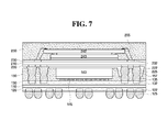
- FIG. 7 is a cross-sectional view illustrating a package on package having an upper semiconductor package stacked on a semiconductor package according to an exemplary embodiment.
- Exemplary embodiments described herein will be described referring to plan views and/or cross-sectional views by way of ideal schematic views. Accordingly, the exemplary views may be modified depending on manufacturing technologies and/or tolerances. Therefore, the exemplary embodiments are not limited to those shown in the views, but include modifications in configuration formed on the basis of manufacturing processes. Therefore, regions exemplified in the figures have schematic properties, and shapes of regions shown in the figures exemplify specific shapes of regions of elements and not intended to limit aspects of the present inventive concept.
- FIG. 1 is a cross-sectional view illustrating a semiconductor package according to an exemplary embodiment.
- the semiconductor package 100 includes a substrate 110 , a semiconductor chip 140 , a plurality of connecting conductors 135 , molding member 150 , and a plurality of connecting via holes 152 and 157 .
- the substrate 110 may be a board for a package, and may include, for example, a printed circuit board or a ceramic board. Further, as shown in FIG. 1 , insulation layers 130 and 120 may be formed on top and bottom surfaces of the substrate 110 , respectively. Pads 132 connected with the plurality of connecting conductors 135 may be formed on the insulation layer 130 formed on the top surface of the substrate 110 . Pads 122 connected with a plurality of solder balls 125 may be formed on the insulation layer 120 formed on the bottom surface of the substrate 110 .
- the plurality of connecting conductors 135 may be connected to connecting conductors formed on the bottom surface of an upper semiconductor package when stacking the plurality of semiconductor packages, to then be electrically connected to the upper semiconductor package.
- the solder balls 125 may electrically connect the semiconductor packages to a module board or a main circuit board.
- the semiconductor chip 140 may be attached to the top surface of the substrate 110 . As illustrated, when the semiconductor chip 140 is referred to as being attached to the top surface of the substrate 110 , it can be directly on or extend directly onto the insulation layer 130 formed on the substrate 110 . For example, FIG. 1 shows the semiconductor chip 140 directly on the insulation layer 130 . However, as just discussed, this is only an example.
- the semiconductor chip 140 may include, for example, a logic device such as a microprocessor, but is not limited thereto.
- the semiconductor chip 140 may be stacked on the substrate 110 by, for example, a flip chip bonding process. Accordingly, the plurality of conductive chip bumps 145 are disposed between the substrate 110 and the semiconductor chip 140 to electrically connect the substrate 110 to the semiconductor chip 140 .
- the plurality of conductive chip bumps 145 may be formed by, for example, a soldering process.
- the plurality of connecting conductors 135 are disposed on the top surface of the substrate 110 .
- the plurality of connecting conductors 135 may be formed of a solder material, and may have a substantially spherical or hemispherical shape.
- the molding member 150 is formed on the substrate 110 and provides spaces for and structural support for the plurality of connecting conductors 135 and the semiconductor chip 140 . More specifically, the molding member 150 may be formed on the top surface of the substrate 110 so as to surround lateral surfaces of the semiconductor chip 140 while filling a space between the semiconductor chip 140 and the substrate 110 . Connecting via holes 152 and 157 to be described later may be formed in the molding member 150 .
- the molding member 150 may include epoxy molding compound (EMC), polyimide, or the like.
- FIG. 1 illustrates an exemplary embodiment in which the top surface of the semiconductor chip 140 is exposed because the molding member 150 has a height that is substantially the same as or less than the height of the semiconductor chip 140 . That is to say, in a case where the top surface of the semiconductor chip 140 is exposed to the outside of the molding member 150 , the overall thickness of the semiconductor package 100 and the overall thickness of a stacked package structure are reduced. In addition, various advantages are rendered, including an improved heat dissipation characteristic, increased resistance with respect to high-temperature processes, and increased resistance against twist. However, the present inventive concept does not limit the molding member 150 to that illustrated herein. Alternatively, the molding member 150 may be formed to extend beyond the height of the semiconductor chip 140 or to cover the semiconductor chip 140 .
- the plurality of connecting via holes 152 and 157 extend through the molding member 150 to expose the plurality of connecting conductors 135 , respectively.
- the plurality of connecting via holes 152 and 157 may be formed by a laser drilling process using a laser. With respect to at least one of the plurality of connecting via holes 152 and 157 , that is, a first connecting via hole 157 , a planar distance from the first connecting conductor 135 exposed by the first connecting via hole 157 to an entrance of the first connecting via hole 157 is not uniform.
- planar distance from the first connecting conductor 135 to an entrance of the first connecting via hole 157 may denote a distance from an outer contour line of the first connecting conductor 135 to an outer contour line of the first connecting via hole 157 when the semiconductor package is viewed from above, that is, in a plane view.
- distances from a planar outer contour line 157 P of at least one of the plurality of connecting via holes 152 and 157 , that is, the first connecting via hole 157 , to a planar outer contour line 135 P of the first connecting conductors 135 is not uniform, as shown on the right-hand side of FIG. 1 .
- planar outer contour line 152 P of connecting via holes 152 disposed on the left-hand side in FIG. 1 are spaced a uniform distance apart from the planar outer contour line 135 P of the connecting conductors 135 . More specifically, as shown in FIG. 1 , when the connecting conductors 135 are spherical or hemispherical, the entrance of the connecting via hole 152 exposing the connecting conductor 135 is also circular. Accordingly, the planar outer contour line 135 P of the connecting conductor 135 and the planar outer contour line 152 P of the connecting via hole 152 are both circular. In addition, the planar outer contour line 135 P of the connecting conductor 135 and the planar outer contour line 152 P of the connecting via hole 152 are concentrically formed.
- the planar outer contour line 157 P of connecting via holes 157 disposed on the right-hand side in FIG. 1 are spaced a non-uniform distance apart from the planar outer contour line 135 P of the first connecting conductors 135 .
- the centers of the planar outer contour line 135 P of the first connecting conductor 135 and the planar outer contour line 157 P of the first connecting via hole 157 may be at different positions from each other.
- the planar outer contour line 135 P of the first connecting conductor 135 and the planar outer contour line 157 P of the first connecting via hole 157 may have the same shape, for example, a circular shape.
- planar outer contour line 135 P of the first connecting conductors 135 and the planar outer contour line 157 P of the first connecting via hole 157 may have different sizes.
- planar shapes of the first connecting conductors 135 and the first connecting via hole 157 may both be real circle shapes.
- the outer contour line 135 P of the first connecting conductors 135 may be disposed within the outer contour line 157 P of the first connecting via hole 157 , or a portion of the outer contour line 135 P of the first connecting conductors 135 may protrude outside the outer contour line 157 P of the first connecting via hole 157 .
- the planar outer contour line 135 P of the first connecting conductors 135 and the planar outer contour line 157 P of the first connecting via hole 157 may have different shapes and different sizes.
- the planar shape of the first connecting conductors 135 may be a real circle shape, and the planar shape of the first connecting via hole 157 may be an oval shape.
- the outer contour line 135 P of the first connecting conductors 135 may be disposed within the outer contour line 157 P of the first connecting via hole 157 , or a portion of the outer contour line 135 P of the first connecting conductors 135 may protrude outside the planar outer contour line 157 P of the first connecting via hole 157 .
- a distance between the planar outer contour line 135 P of the first connecting conductor 135 and the planar outer contour line 157 P of the first connecting via hole 157 is not uniform.
- the center of the first connecting conductor 135 and the center of the first connecting via hole 157 may be positioned at different positions. Accordingly, the center of the planar outer contour line 135 P of the first connecting conductor 135 and the center of the planar outer contour line 157 P of the first connecting via hole 157 might not be concentric in some cases.
- the center of at least one first connecting via hole 157 of the plurality of connecting via holes 152 and 157 may be positioned at a position different from that of the first connecting conductors 135 that are exposed by the first connecting via hole 157 .
- the center of the first connecting conductors 135 and the center of the first connecting via hole 157 may denote the center of the planar outer contour line 135 P of the first connecting conductor 135 and the center of the planar outer contour line 157 P of the first connecting via hole 157 , respectively.
- the center of the first connecting conductor 135 and the center of the first connecting via hole 157 may be positioned at the same position.
- a distance between the planar outer contour line 135 P of the first connecting conductor 135 and the planar outer contour line 157 P of the first connecting via hole 157 is still not uniform.
- a planar shape of the first connecting conductor 135 may be a real circle shape, and a planar shape of the first connecting via hole 157 may be an oval shape while still having the same center.
- the first connecting via hole 157 exposing the first connecting conductor 135 may be formed in various shapes to prevent a connecting conductor disposed within the first connecting via hole 157 from outflowing from the first connecting via hole 157 and contacting an adjacent connecting conductor.
- a space can be formed within the first connecting via hole 157 in which the connecting conductor is disposed by varying arrangement relationships between the first connecting via hole 157 and the first connecting conductor 135 , that is, planar shapes, center positions, a distance between outer contour lines, etc.
- the connecting via hole having various shapes can be more easily formed.
- FIGS. 2A to 2C are plan views illustrating arrangement of a first connecting via hole relative to a first connecting conductor
- FIGS. 3A to 3C are cross-sectional views illustrating variously shaped sidewalls of the first connecting via hole.
- the plurality of connecting conductors may include a first connecting conductor 135 a and a second connecting conductor 135 b disposed in adjacent with each other, and a plurality of connecting via holes may include a first connecting via hole 157 a exposing the first connecting conductor 135 a and a second connecting via hole 157 b exposing the second connecting conductor 135 b.
- the center A 1 of the first connecting conductor 135 a and the center B 1 of the first connecting via hole 157 a may be positioned at different positions.
- the center A 2 of the second connecting conductor 157 a and the center B 2 of the second connecting via hole 157 b may also be positioned at different positions.
- first distance D 1 a distance between the center A 1 of the first connecting conductor 135 a and the center A 2 of the second connecting conductor 135 b
- second distance D 2 a distance between the center B 1 of the first connecting via hole 157 b and the center B 2 of the second connecting via hole 157 b
- the second distance D 2 may be greater than the first distance D 1 .
- a planar distance between the first connecting via hole 157 a and the first connecting conductor 135 a is reduced as outer contour lines of the first connecting via hole 157 a and the first connecting conductor 135 a become closer to the second connecting conductor 135 b .
- a planar distance between the first connecting via hole 157 a and the first connecting conductor 135 a is increased as outer contour lines of the first connecting via hole 157 a and the first connecting conductor 135 a become farther from the second connecting conductor 135 b .
- an internal space of the molding member 150 provided by the first connecting via hole 157 a and the second connecting via hole 157 b is small in a region where the first connecting conductor 135 a and the second connecting conductor 135 b are adjacent to each other, and the internal space of the molding member 150 provided by the first connecting via hole 157 a and the second connecting via hole 157 b is large in a region where the first connecting conductor 135 a and the second connecting conductor 135 b are spaced apart from each other, making the internal space serve as a kind of buffer space.
- the connecting conductors of the upper semiconductor package when connected to the first connecting conductor 135 a and the second connecting conductor 135 b , they may extend toward the relatively wide space to the outside of the first and second connecting conductors 135 a , 135 b as shown in FIG. 2A , that is, to a region where the first connecting conductor 135 a and the second connecting conductor 135 b are spaced apart from each other, thereby preventing a short circuit between adjacent connecting conductors.
- planar shapes of the first connecting conductor 135 a and the second connecting conductor 135 b may be the same as those of the first connecting via hole 157 a and the second connecting via hole 157 b , while sizes of the first connecting conductor 135 a and the second connecting conductor 135 b may be different from those of the first connecting via hole 157 a and the second connecting via hole 157 b .
- first connecting via hole 157 a and the second connecting via hole 157 b are all formed in real circle shapes, and sizes, e.g., diameters, of the real circle shapes of the first connecting via hole 157 a and the second connecting via hole 157 b may be larger than sizes, e.g., diameters, of the first connecting conductor 135 a and the second connecting conductor 135 b . Accordingly, when the first connecting conductor 135 a and the second connecting conductor 135 b are disposed within the first connecting via hole 157 a and the second connecting via hole 157 b , respectively, a sufficient large buffer region for connecting the connecting conductors of the upper semiconductor package can be secured. Therefore, a short circuit between adjacent connecting conductors can be prevented.
- FIG. 2A illustrates that the centers of the first connecting conductor 135 a and the second connecting conductor 135 b which are adjacent to each other are positioned at different positions from the centers of the first connecting via hole 157 a and the second connecting via hole 157 b .
- the center of at least one of the first connecting conductor 135 a and the second connecting conductor 135 b for example, the center A 1 of the first connecting conductor 135 a , and the center B 1 of the first connecting via hole 157 a are disposed at different positions, and the center A 2 of the second connecting conductor 135 b and the center B 2 of the second connecting via hole 157 b may be positioned at the same position.
- the center A 1 of the first connecting conductor 135 a and the center B 1 of the first connecting via hole 157 a are still disposed at different positions from the center A 2 of the second connecting conductor 135 b and the center B 2 of the second connecting via hole 157 b.
- first distance D 1 a distance between the center A 1 of the first connecting conductor 135 a and the center A 2 of the second connecting conductor 135 b
- second distance D 2 a distance between the center B 1 of the first connecting via hole 157 b and the center B 2 of the second connecting via hole 157 b
- the second distance D 2 may be greater than the first distance D 1 .
- a planar shape of the first connecting conductor 135 a and the second connecting conductor 135 b and a planar shape of first connecting via hole 157 a and the second connecting via hole 157 b may be different from each other.
- the planar shapes of the first connecting conductor 135 a and the second connecting conductor 135 b may be real circle shapes while the planar shapes of the first connecting via hole 157 a and the second connecting via hole 157 b may be oval shapes.
- first connecting via hole 157 a and the second connecting via hole 157 b extending through the molding member 150 are formed to have different planar shapes as those of the first connecting conductor 135 a and the second connecting conductor 135 b , a sufficiently large buffer region for connecting conductors of the upper semiconductor package can be secured on the first connecting conductor 135 a and the second connecting conductor 135 b disposed within the first connecting via hole 157 a and the second connecting via hole 157 b , respectively. Therefore, a short circuit between adjacent connecting conductors can be prevented.
- FIG. 2B illustrates that the centers of the first connecting conductor 135 a and the second connecting conductor 135 b are both disposed at different positions from the centers of the first connecting via hole 157 a and the second connecting via hole 157 b , respectively.
- the center of at least one of the first connecting conductor 135 a and the second connecting conductor 135 b disposed adjacent to each other for example, the center A 1 of the first connecting conductor 135 a may be positioned at a position different from the center B 1 of the first connecting via hole 157 a , and the center A 2 of the second connecting conductor 135 b may be positioned at the same position as the center B 2 of the second connecting via hole 157 b.
- the center A 1 of the first connecting conductor 135 a and the center B 1 of the first connecting via hole 157 a may be positioned at the same position.
- the center A 2 of the second connecting conductor 135 b and the center B 2 of the second connecting via hole 157 b may also be positioned at the same position.
- a planar distance from the first and second connecting conductors 135 a and 135 b to entrances of the first and second connecting via holes 157 a and 157 b , respectively, may not be uniform.
- the first and second connecting conductors 135 a and 135 b may have different shapes from those of the first and second connecting via holes 157 a and 157 b , respectively.
- planar shapes of the first and second connecting conductors 135 a and 135 b may be real circle shapes, and planar shapes of the first and second connecting via holes 157 a and 157 b may be oval shapes.
- a sufficiently large buffer region for connecting the connecting conductors of the upper semiconductor package can be secured on the first connecting conductor 135 a and the second connecting conductor 135 b disposed within the first connecting via hole 157 a and the second connecting via hole 157 b , respectively, extending through the molding member 150 by forming the first connecting via hole 157 a and the second connecting via hole 157 b to have different planar shapes as those of the first connecting conductor 135 a and the second connecting conductor 135 b , respectively.
- each of the connecting via holes 157 a and 157 b may have a long axis and a short axis.
- the long axis denotes a line connecting two focuses of the oval
- the short axis denotes a line perpendicular to the line connecting two focuses of the oval.
- the long axes of the first connecting via hole 157 a and the second connecting via hole 157 b may be disposed on a line M connecting the center A 1 of the first connecting conductor 135 a and the center A 2 of the second connecting conductor 135 b .
- the long axes of the first connecting via hole 157 a and the second connecting via hole 157 b may be disposed perpendicular to the center line M connecting the center A 1 of the first connecting conductor 135 a and the center A 2 of the second connecting conductor 135 b.
- the long axis of each of the connecting via holes 157 a and 157 b may be arranged in various manners relative to the center line M.
- the center B 1 of the first connecting via hole 157 a and the center A 1 of the first connecting conductor 135 a are disposed at the same position, the long axis of the first connecting via hole 157 a is at an angle other than 0 degrees with respect to the center line M.
- FIGS. 2A to 2C illustrate the first and second connecting conductors 135 a and 135 b and the first and second connecting via holes 157 a and 157 b are arranged perpendicular to the center line M and symmetrical to the line passing the mid point of the center A 1 of the first connecting conductor 135 a and the center A 2 of the second connecting conductor 135 b
- the present inventive concept is not limited thereto.
- the planar shape and the center position of the first connecting via hole 157 a may be different from those of the second connecting via hole 157 b.
- first and second sidewalls S 1 and S 2 of the first and second connecting via holes 157 a and 157 b may have different shapes.
- first connecting via hole 157 a and the second connecting via hole 157 b may each have a first sidewall S 1 and a second sidewall S 2 defined as surfaces of the molding member 150 .
- first sidewall S 1 and the second sidewall S 2 of the first and second connecting via holes 157 a and 157 b may have a first slope ⁇ 1 and a second slope ⁇ 2 , respectively, with respect to the surface of the molding member.
- first sidewall S 1 of the first connecting via hole 157 a may have a first slope ⁇ 1
- second sidewall S 2 of the first connecting via hole 157 b may have a second slope ⁇ 2
- first sidewall S 1 of the second connecting via hole 157 b may have the first slope ⁇ 1
- second sidewall S 2 of the second connecting via hole 157 b may have the second slope ⁇ 2 .
- first slope ⁇ 1 and the second slope ⁇ 2 of the first connecting via hole 157 a may be the same with each other.
- the second connecting via hole 157 b may have a first sidewall S 1 and a second sidewall S 2 having the same slope.
- first sidewall S 1 opposite to the second sidewall S 2 at which the first connecting conductor 135 a and the second connecting conductor 135 b are disposed may be farther from the first connecting conductor 135 a and the second connecting conductor 135 b than the second sidewall S 2 .
- the first slope ⁇ 1 of the first sidewall S 1 and the second slope ⁇ 2 of the second sidewall S 2 of each connecting via hole may be different from each other.
- the second sidewalls S 2 of the first connecting via hole 157 a and the second connecting via hole 157 b are closer to each other than the first sidewalls S 1 of the first connecting via hole 157 a and the second connecting via hole 157 b .
- the second slope ⁇ 2 of the first connecting via hole 157 a is larger than the first slope ⁇ 1 of the first connecting via hole 157 a and the second slope ⁇ 2 of the second connecting via hole 157 b is larger than the first slope ⁇ 1 of the second connecting via hole 157 b.
- FIG. 3C illustrates at least one of the first sidewall S 1 and the second sidewall S 2 of at least one of the first connecting via hole 157 a and the second connecting via hole 157 b may be formed stepwise.
- FIG. 3C illustrates the second sidewall S 2 of the first connecting via hole 157 a and the second sidewall S 2 of the second connecting via hole 157 b are formed in a tilted manner, and the first sidewalls S 1 of the first connecting via hole 157 a and the second connecting via hole 157 b opposite to the second sidewalls S 2 are formed stepwise.
- FIG. 3C illustrates only an exemplary embodiment, and alternative embodiments may also be made.
- At least one of the first sidewall S 1 and the second sidewall S 2 of the first connecting via hole 157 a and at least one of the first sidewall S 1 and the second sidewall S 2 of the second connecting via hole 157 b may be formed stepwise.
- the variously shaped sidewalls capable of providing a buffer region in a connecting via hole may be implemented.
- connecting via holes having various shapes can be easily formed.
- FIGS. 2A to 2C and FIGS. 3A to 3C can be combined in various manners.
- at least one of sidewalls may be formed stepwise while forming connecting conductors and connecting via holes in planarly real circle shapes.
- FIG. 4 is a view illustrating a connecting conductor region to define a plurality of connecting conductors arranged on a substrate
- FIG. 5 is a partially enlarged view of an ‘A’ portion of FIG. 4 .
- the substrate 110 includes connecting conductor regions a and b in which the plurality of connecting conductors 135 are arranged, the connecting conductor regions a and b corresponding to sides of the substrate 110 and corners of the substrate 110 , respectively. While FIG. 4 illustrates that the connecting conductors 135 are arranged in a row in the first region a, they may also be arranged in a plurality of rows, or in a non-uniform arrangement.
- a group of connecting conductors arranged in the second region b may be exposed according to the first connecting via hole 157 . More specifically, planar distances from the connecting conductors 135 arranged in the second region b to entrances of the corresponding connecting via holes 157 are not uniform. Alternatively, centers of the connecting conductors 135 arranged in the second region b may be different from the centers of the corresponding connecting via holes 157 . Alternatively, centers of the connecting conductors 135 arranged in the second region b may have different planar shapes from those of centers of the corresponding connecting via holes 157 while being at the same positions as the center of the corresponding connecting via holes 157 . Here, planar distances from the connecting conductors 135 arranged in the second region a to entrances of connecting via holes 152 may be uniform.
- the connecting via holes 157 having various shapes can be more easily formed, thereby reducing processing burdens.
- the connecting via holes 157 having various shapes can be employed in both the connecting conductor regions a and b where the plurality of connecting conductors 135 are disposed as well as the corner region. That is to say, the connecting conductors 135 disposed in the first region a and the second region b may be exposed by the connecting via holes 157 having various shapes.
- a planar distance from the contour line of the connecting conductors 135 to the contour line of the contour line of the connecting via holes 157 may be made such that they are not uniform.
- FIG. 6 is a view illustrating a process of stacking an upper semiconductor package on a semiconductor package according to an exemplary embodiment
- FIG. 7 is a cross-sectional view illustrating a package on package having an upper semiconductor package stacked on a semiconductor package according to an exemplary embodiment.
- the first semiconductor package 100 shown in FIGS. 6 and 7 has the same configuration as the semiconductor packages according to the above-described exemplary embodiments, a detailed description thereof will be omitted.
- the package on package includes a first semiconductor package 100 and a second semiconductor package 200 .
- the first semiconductor package 100 may be referred to as a lower semiconductor package and the second semiconductor package 200 may be referred to as an upper semiconductor package.
- the first semiconductor package 100 includes a first substrate 110 , a first semiconductor chip 140 attached to a top surface of the first substrate 110 , a plurality of connecting conductors 135 disposed on the top surface of the first substrate 110 , a molding member 150 formed on the first substrate 110 to provide space and structural support for the plurality of connecting conductors 135 and the first semiconductor chip 140 , and a plurality of connecting via holes 152 and 157 extending through the molding member 150 to expose the plurality of connecting conductors 135 , respectively.
- the second semiconductor package 200 includes a second substrate 210 , and a second semiconductor chip 240 attached to a top surface of the second substrate 210 . The second semiconductor package 200 is stacked on the first semiconductor package 100 .
- a planar distance from a first connecting conductor 135 exposed by at least one of the plurality of connecting via holes 152 and 157 , that is, a first connecting via hole 157 , of the first semiconductor package 100 , to an entrance of the first connecting via hole 157 is not uniform.
- the semiconductor package 100 may be applied to the lower semiconductor package 100 of the package on package shown in FIGS. 6 and 7 .
- the connecting via holes 157 shown in FIGS. 2A to 2C and FIGS. 3A to 3C may be applied to at least one of the plurality of connecting via holes 152 and 157 of the lower semiconductor package 100 .
- At least one of the connecting via holes 152 and 157 exposing the connecting conductors 135 of the lower semiconductor package 100 may include a buffer space for connecting conductors 225 of the upper semiconductor package 200 . Therefore, even if the connecting conductors 135 of the lower semiconductor package 100 are connected to the connecting conductor 225 of the upper semiconductor package 200 , it is possible to prevent the first connecting via hole 157 from outflowing.
Abstract
A semiconductor package and a package on package are provided. The semiconductor package includes a substrate; a semiconductor chip attached to a surface of the substrate; connecting conductors disposed on the surface of the substrate; a mold formed on the substrate and in which the connecting conductors and the semiconductor chip are provided; and connecting via holes extending through the mold and exposing the connecting conductors. With respect to a first connecting via hole of the connecting via holes, a planar distance between a first connecting conductor exposed by the first connecting via hole and an entrance of the first connecting via hole is not uniform.
Description
This application is a Continuation of U.S. application Ser. No. 13/244,506, filed on Sep. 25, 2011, now U.S. Pat. No. 8,531,032, which claims priority from Korean Patent Application No. 10-2010-0131508 filed on Dec. 21, 2010 in the Korean Intellectual Property Office, the contents of which in its entirety are herein incorporated by reference.
1. Field
Exemplary embodiments to a semiconductor package and a package on package having the same.
2. Description of the Related Art
Semiconductor packages are increasingly developed to meet requirements including multiple functions, high capacity, compactness, and small size. To keep pace with the development, a system in package (SIP) has been proposed, in which multiple semiconductor packages are integrated into one single semiconductor package, enabling high capacity and multiple functions while reducing the size of the semiconductor package.
One technology implemented in the SIP is to vertically stack semiconductor packages that are individually assembled and have undergone electric tests. This is referred to as a package on package (POP) or a stacked package.
In general, when an upper semiconductor package is stacked on a lower semiconductor package, a plurality of connecting conductors are used to electrically connect the lower semiconductor package and the upper semiconductor package. Here, a connecting conductor of the lower semiconductor package and a connecting conductor of the upper semiconductor package may be connected to each other through connecting via holes.
However, as semiconductor packages become smaller, a pitch between the connecting via holes gradually decreases. Accordingly, internal spaces of the connecting via holes are filled up by the connecting conductors of the upper and lower semiconductor packages, causing overflow, and short circuits between adjacent connecting conductors.
One or more exemplary embodiments provide a semiconductor package which can prevent short circuit between adjacent connecting conductors.
One or more exemplary embodiments also provide a package on package which can prevent short circuit between adjacent connecting conductors.
According to an aspect of an exemplary embodiment, there is provided a semiconductor package including a substrate; a semiconductor chip attached to a surface of the substrate; a plurality of connecting conductors disposed on the surface of the substrate; a molding member formed on the substrate and in which the plurality of connecting conductors and the semiconductor chip are provided; and a plurality of connecting via holes extending through the molding member and exposing the plurality of connecting conductors, respectively, wherein with respect to a first connecting via hole of the plurality of connecting via holes, a planar distance between a first connecting conductor exposed by the first connecting via hole and an entrance of the first connecting via hole is not uniform.
According to another aspect of an exemplary embodiment, there is provided a semiconductor package including a substrate; a semiconductor chip attached to a surface of the substrate; a plurality of connecting conductors disposed on the surface of the substrate; a molding member formed on the substrate and having a space for the plurality of connecting conductors and the semiconductor chip; and a plurality of connecting via holes extending through the molding member and exposing the plurality of connecting conductors, respectively, wherein a center of a first connecting via hole among the plurality of connecting via holes is at a different position from a center of a corresponding first connecting conductor with respect to the substrate.
According to another aspect of an exemplary embodiment, there is provided a package on package including a first semiconductor package including a first substrate, a first semiconductor chip attached to a surface of the first substrate, a plurality of connecting conductors disposed on the surface of the first substrate, a molding member formed on the first substrate and having a space for the plurality of connecting conductors and the first semiconductor chip, and a plurality of connecting via holes extending through the molding member and exposing the plurality of connecting conductors, respectively; and a second semiconductor package including a second substrate and a second semiconductor chip attached to a surface of the second substrate and stacked on the first semiconductor package, wherein with respect to a first connecting via hole of the plurality of connecting via holes of the first semiconductor package, a planar distance between a first connecting conductor exposed by the first connecting via hole and an entrance of the first connecting via hole is not uniform.
According to another aspect of an exemplary embodiment, there is provided a semiconductor package, the semiconductor package including a substrate; a semiconductor chip attached to a surface of the substrate; a plurality of connecting conductors which provide connections to the semiconductor ship; and a mold formed on the substrate for holding the semiconductor chip and comprising a plurality of via holes which expose corresponding ones of the connecting conductors through the mold, wherein, for a first via hole of the plurality of via holes, a planar distance between a connecting conductor exposed by the first via hole and an entrance of the first via hole is not uniform.
The above and other aspects will become more apparent by describing in detail exemplary embodiments with reference to the attached drawings in which:
Advantages and features of the present inventive concept and methods of accomplishing the same may be understood more readily by reference to the following detailed description of exemplary embodiments and the accompanying drawings. The present inventive concept may, however, be embodied in many different forms and should not be construed as being limited to the exemplary embodiments set forth herein. Rather, these exemplary embodiments are provided so that this disclosure will be thorough and complete and will fully convey the present inventive concept to those skilled in the art, and the present inventive concept will only be defined by the appended claims. In the drawings, the thickness of layers and regions are exaggerated for clarity.
It will be understood that when an element such as a layer, region or substrate is referred to as being “on” or extending “onto” another element, it can be directly on or extend directly onto the other element or intervening elements may also be present. In contrast, when an element is referred to as being “directly on” or extending “directly onto” another element, there are no intervening elements present. It will also be understood that when an element is referred to as being “connected” or “coupled” to another element, it can be directly connected or coupled to the other element or intervening elements may be present. In contrast, when an element is referred to as being “directly connected” or “directly coupled” to another element, there are no intervening elements present.
Like numbers refer to like elements throughout. As used herein, the term “and/or” includes any and all combinations of one or more of the associated listed items.
Spatially relative terms, such as “below,” “beneath,” “lower,” “above,” “upper,” and the like, may be used herein for ease of description to describe one element or feature's relationship to another element(s) or feature(s) as illustrated in the figures. It will be understood that the spatially relative terms are intended to encompass different orientations of the device in use or operation in addition to the orientation depicted in the figures.
Exemplary embodiments described herein will be described referring to plan views and/or cross-sectional views by way of ideal schematic views. Accordingly, the exemplary views may be modified depending on manufacturing technologies and/or tolerances. Therefore, the exemplary embodiments are not limited to those shown in the views, but include modifications in configuration formed on the basis of manufacturing processes. Therefore, regions exemplified in the figures have schematic properties, and shapes of regions shown in the figures exemplify specific shapes of regions of elements and not intended to limit aspects of the present inventive concept.
First, a semiconductor package according to an exemplary embodiment will be described. FIG. 1 is a cross-sectional view illustrating a semiconductor package according to an exemplary embodiment.
Referring to FIG. 1 , the semiconductor package 100 includes a substrate 110, a semiconductor chip 140, a plurality of connecting conductors 135, molding member 150, and a plurality of connecting via holes 152 and 157.
The substrate 110 may be a board for a package, and may include, for example, a printed circuit board or a ceramic board. Further, as shown in FIG. 1 , insulation layers 130 and 120 may be formed on top and bottom surfaces of the substrate 110, respectively. Pads 132 connected with the plurality of connecting conductors 135 may be formed on the insulation layer 130 formed on the top surface of the substrate 110. Pads 122 connected with a plurality of solder balls 125 may be formed on the insulation layer 120 formed on the bottom surface of the substrate 110.
The plurality of connecting conductors 135 may be connected to connecting conductors formed on the bottom surface of an upper semiconductor package when stacking the plurality of semiconductor packages, to then be electrically connected to the upper semiconductor package. In addition, the solder balls 125 may electrically connect the semiconductor packages to a module board or a main circuit board.
The semiconductor chip 140 may be attached to the top surface of the substrate 110. As illustrated, when the semiconductor chip 140 is referred to as being attached to the top surface of the substrate 110, it can be directly on or extend directly onto the insulation layer 130 formed on the substrate 110. For example, FIG. 1 shows the semiconductor chip 140 directly on the insulation layer 130. However, as just discussed, this is only an example. The semiconductor chip 140 may include, for example, a logic device such as a microprocessor, but is not limited thereto.
The semiconductor chip 140 may be stacked on the substrate 110 by, for example, a flip chip bonding process. Accordingly, the plurality of conductive chip bumps 145 are disposed between the substrate 110 and the semiconductor chip 140 to electrically connect the substrate 110 to the semiconductor chip 140. The plurality of conductive chip bumps 145 may be formed by, for example, a soldering process.
The plurality of connecting conductors 135 are disposed on the top surface of the substrate 110. The plurality of connecting conductors 135 may be formed of a solder material, and may have a substantially spherical or hemispherical shape.
The molding member 150 is formed on the substrate 110 and provides spaces for and structural support for the plurality of connecting conductors 135 and the semiconductor chip 140. More specifically, the molding member 150 may be formed on the top surface of the substrate 110 so as to surround lateral surfaces of the semiconductor chip 140 while filling a space between the semiconductor chip 140 and the substrate 110. Connecting via holes 152 and 157 to be described later may be formed in the molding member 150. The molding member 150 may include epoxy molding compound (EMC), polyimide, or the like.
The plurality of connecting via holes 152 and 157 extend through the molding member 150 to expose the plurality of connecting conductors 135, respectively. The plurality of connecting via holes 152 and 157 may be formed by a laser drilling process using a laser. With respect to at least one of the plurality of connecting via holes 152 and 157, that is, a first connecting via hole 157, a planar distance from the first connecting conductor 135 exposed by the first connecting via hole 157 to an entrance of the first connecting via hole 157 is not uniform.
The term “planar distance from the first connecting conductor 135 to an entrance of the first connecting via hole 157” used herein may denote a distance from an outer contour line of the first connecting conductor 135 to an outer contour line of the first connecting via hole 157 when the semiconductor package is viewed from above, that is, in a plane view.
As shown in FIG. 1 , distances from a planar outer contour line 157P of at least one of the plurality of connecting via holes 152 and 157, that is, the first connecting via hole 157, to a planar outer contour line 135P of the first connecting conductors 135 is not uniform, as shown on the right-hand side of FIG. 1 .
By contrast, the planar outer contour line 152P of connecting via holes 152 disposed on the left-hand side in FIG. 1 are spaced a uniform distance apart from the planar outer contour line 135P of the connecting conductors 135. More specifically, as shown in FIG. 1 , when the connecting conductors 135 are spherical or hemispherical, the entrance of the connecting via hole 152 exposing the connecting conductor 135 is also circular. Accordingly, the planar outer contour line 135P of the connecting conductor 135 and the planar outer contour line 152P of the connecting via hole 152 are both circular. In addition, the planar outer contour line 135P of the connecting conductor 135 and the planar outer contour line 152P of the connecting via hole 152 are concentrically formed.
On the other hand, returning to the examples on the right-hand side of FIG. 1 , the planar outer contour line 157P of connecting via holes 157 disposed on the right-hand side in FIG. 1 are spaced a non-uniform distance apart from the planar outer contour line 135P of the first connecting conductors 135. Moreover, the centers of the planar outer contour line 135P of the first connecting conductor 135 and the planar outer contour line 157P of the first connecting via hole 157 may be at different positions from each other. In this case, as shown in the example on the right-hand side of FIG. 1 , the planar outer contour line 135P of the first connecting conductor 135 and the planar outer contour line 157P of the first connecting via hole 157 may have the same shape, for example, a circular shape.
However, the planar outer contour line 135P of the first connecting conductors 135 and the planar outer contour line 157P of the first connecting via hole 157 may have different sizes. For example, planar shapes of the first connecting conductors 135 and the first connecting via hole 157 may both be real circle shapes. Here, the outer contour line 135P of the first connecting conductors 135 may be disposed within the outer contour line 157P of the first connecting via hole 157, or a portion of the outer contour line 135P of the first connecting conductors 135 may protrude outside the outer contour line 157P of the first connecting via hole 157.
In some other exemplary embodiments, the planar outer contour line 135P of the first connecting conductors 135 and the planar outer contour line 157P of the first connecting via hole 157 may have different shapes and different sizes. In such cases, for example, the planar shape of the first connecting conductors 135 may be a real circle shape, and the planar shape of the first connecting via hole 157 may be an oval shape. Likewise the outer contour line 135P of the first connecting conductors 135 may be disposed within the outer contour line 157P of the first connecting via hole 157, or a portion of the outer contour line 135P of the first connecting conductors 135 may protrude outside the planar outer contour line 157P of the first connecting via hole 157.
That is to say, as shown in the right side of FIG. 1 , with respect to one of the first connecting conductors 135, a distance between the planar outer contour line 135P of the first connecting conductor 135 and the planar outer contour line 157P of the first connecting via hole 157 is not uniform. In this case, the center of the first connecting conductor 135 and the center of the first connecting via hole 157 may be positioned at different positions. Accordingly, the center of the planar outer contour line 135P of the first connecting conductor 135 and the center of the planar outer contour line 157P of the first connecting via hole 157 might not be concentric in some cases.
In other words, the center of at least one first connecting via hole 157 of the plurality of connecting via holes 152 and 157 may be positioned at a position different from that of the first connecting conductors 135 that are exposed by the first connecting via hole 157. As described above, the center of the first connecting conductors 135 and the center of the first connecting via hole 157 may denote the center of the planar outer contour line 135P of the first connecting conductor 135 and the center of the planar outer contour line 157P of the first connecting via hole 157, respectively.
Further, in some other exemplary embodiments, the center of the first connecting conductor 135 and the center of the first connecting via hole 157 may be positioned at the same position. In this case, a distance between the planar outer contour line 135P of the first connecting conductor 135 and the planar outer contour line 157P of the first connecting via hole 157 is still not uniform. For example, a planar shape of the first connecting conductor 135 may be a real circle shape, and a planar shape of the first connecting via hole 157 may be an oval shape while still having the same center.
In the semiconductor package according to exemplary embodiments, the first connecting via hole 157 exposing the first connecting conductor 135 may be formed in various shapes to prevent a connecting conductor disposed within the first connecting via hole 157 from outflowing from the first connecting via hole 157 and contacting an adjacent connecting conductor. In other words, a space can be formed within the first connecting via hole 157 in which the connecting conductor is disposed by varying arrangement relationships between the first connecting via hole 157 and the first connecting conductor 135, that is, planar shapes, center positions, a distance between outer contour lines, etc. Further, in a case of using laser drilling when a connecting via hole is formed, the connecting via hole having various shapes can be more easily formed.
Hereinafter, various arrangements of the first and second connecting via holes relative to first and second connecting conductors, respectively, will be described with reference to FIGS. 2A to 2C and FIGS. 3A to 3C . FIGS. 2A to 2C are plan views illustrating arrangement of a first connecting via hole relative to a first connecting conductor, and FIGS. 3A to 3C are cross-sectional views illustrating variously shaped sidewalls of the first connecting via hole.
The plurality of connecting conductors may include a first connecting conductor 135 a and a second connecting conductor 135 b disposed in adjacent with each other, and a plurality of connecting via holes may include a first connecting via hole 157 a exposing the first connecting conductor 135 a and a second connecting via hole 157 b exposing the second connecting conductor 135 b.
As shown in FIG. 2A , the center A1 of the first connecting conductor 135 a and the center B1 of the first connecting via hole 157 a may be positioned at different positions. In addition, the center A2 of the second connecting conductor 157 a and the center B2 of the second connecting via hole 157 b may also be positioned at different positions. Alternatively, assuming that a distance between the center A1 of the first connecting conductor 135 a and the center A2 of the second connecting conductor 135 b is denoted as a first distance D1 and a distance between the center B1 of the first connecting via hole 157 b and the center B2 of the second connecting via hole 157 b is denoted as a second distance D2, the second distance D2 may be greater than the first distance D1.
Accordingly, a planar distance between the first connecting via hole 157 a and the first connecting conductor 135 a is reduced as outer contour lines of the first connecting via hole 157 a and the first connecting conductor 135 a become closer to the second connecting conductor 135 b. In addition, a planar distance between the first connecting via hole 157 a and the first connecting conductor 135 a is increased as outer contour lines of the first connecting via hole 157 a and the first connecting conductor 135 a become farther from the second connecting conductor 135 b. In other words, an internal space of the molding member 150 provided by the first connecting via hole 157 a and the second connecting via hole 157 b is small in a region where the first connecting conductor 135 a and the second connecting conductor 135 b are adjacent to each other, and the internal space of the molding member 150 provided by the first connecting via hole 157 a and the second connecting via hole 157 b is large in a region where the first connecting conductor 135 a and the second connecting conductor 135 b are spaced apart from each other, making the internal space serve as a kind of buffer space.
Accordingly, when the connecting conductors of the upper semiconductor package are connected to the first connecting conductor 135 a and the second connecting conductor 135 b, they may extend toward the relatively wide space to the outside of the first and second connecting conductors 135 a, 135 b as shown in FIG. 2A , that is, to a region where the first connecting conductor 135 a and the second connecting conductor 135 b are spaced apart from each other, thereby preventing a short circuit between adjacent connecting conductors.
As shown, planar shapes of the first connecting conductor 135 a and the second connecting conductor 135 b may be the same as those of the first connecting via hole 157 a and the second connecting via hole 157 b, while sizes of the first connecting conductor 135 a and the second connecting conductor 135 b may be different from those of the first connecting via hole 157 a and the second connecting via hole 157 b. For example, the first and second connecting conductor 135 a and 135 b and the first and second connecting via holes 157 a and 157 b in FIG. 2A are all formed in real circle shapes, and sizes, e.g., diameters, of the real circle shapes of the first connecting via hole 157 a and the second connecting via hole 157 b may be larger than sizes, e.g., diameters, of the first connecting conductor 135 a and the second connecting conductor 135 b. Accordingly, when the first connecting conductor 135 a and the second connecting conductor 135 b are disposed within the first connecting via hole 157 a and the second connecting via hole 157 b, respectively, a sufficient large buffer region for connecting the connecting conductors of the upper semiconductor package can be secured. Therefore, a short circuit between adjacent connecting conductors can be prevented.
Referring FIG. 2B , the center A1 of the first connecting conductor 135 a and the center B1 of the first connecting via hole 157 a are still disposed at different positions from the center A2 of the second connecting conductor 135 b and the center B2 of the second connecting via hole 157 b.
Likewise, assuming that a distance between the center A1 of the first connecting conductor 135 a and the center A2 of the second connecting conductor 135 b is denoted as a first distance D1 and a distance between the center B1 of the first connecting via hole 157 b and the center B2 of the second connecting via hole 157 b is denoted as a second distance D2, the second distance D2 may be greater than the first distance D1.
However, as shown in FIG. 2B , a planar shape of the first connecting conductor 135 a and the second connecting conductor 135 b and a planar shape of first connecting via hole 157 a and the second connecting via hole 157 b may be different from each other. For example, the planar shapes of the first connecting conductor 135 a and the second connecting conductor 135 b may be real circle shapes while the planar shapes of the first connecting via hole 157 a and the second connecting via hole 157 b may be oval shapes.
As described above, since the first connecting via hole 157 a and the second connecting via hole 157 b extending through the molding member 150 are formed to have different planar shapes as those of the first connecting conductor 135 a and the second connecting conductor 135 b, a sufficiently large buffer region for connecting conductors of the upper semiconductor package can be secured on the first connecting conductor 135 a and the second connecting conductor 135 b disposed within the first connecting via hole 157 a and the second connecting via hole 157 b, respectively. Therefore, a short circuit between adjacent connecting conductors can be prevented.
Further, FIG. 2B illustrates that the centers of the first connecting conductor 135 a and the second connecting conductor 135 b are both disposed at different positions from the centers of the first connecting via hole 157 a and the second connecting via hole 157 b, respectively. However, in some other exemplary embodiments, the center of at least one of the first connecting conductor 135 a and the second connecting conductor 135 b disposed adjacent to each other, for example, the center A1 of the first connecting conductor 135 a may be positioned at a position different from the center B1 of the first connecting via hole 157 a, and the center A2 of the second connecting conductor 135 b may be positioned at the same position as the center B2 of the second connecting via hole 157 b.
Referring to FIG. 2C , the center A1 of the first connecting conductor 135 a and the center B1 of the first connecting via hole 157 a may be positioned at the same position. In addition, the center A2 of the second connecting conductor 135 b and the center B2 of the second connecting via hole 157 b may also be positioned at the same position. Here, similar to the case described above, a planar distance from the first and second connecting conductors 135 a and 135 b to entrances of the first and second connecting via holes 157 a and 157 b, respectively, may not be uniform. The first and second connecting conductors 135 a and 135 b may have different shapes from those of the first and second connecting via holes 157 a and 157 b, respectively. For example, planar shapes of the first and second connecting conductors 135 a and 135 b may be real circle shapes, and planar shapes of the first and second connecting via holes 157 a and 157 b may be oval shapes.
As described above, a sufficiently large buffer region for connecting the connecting conductors of the upper semiconductor package can be secured on the first connecting conductor 135 a and the second connecting conductor 135 b disposed within the first connecting via hole 157 a and the second connecting via hole 157 b, respectively, extending through the molding member 150 by forming the first connecting via hole 157 a and the second connecting via hole 157 b to have different planar shapes as those of the first connecting conductor 135 a and the second connecting conductor 135 b, respectively.
Therefore, a short circuit between adjacent connecting conductors can be prevented.
As shown in FIGS. 2B and 2C , when the first connecting via hole 157 a and the second connecting via hole 157 b are formed to have planarly oval shapes, the planar shape of each of the connecting via holes 157 a and 157 b may have a long axis and a short axis. Here, the long axis denotes a line connecting two focuses of the oval, and the short axis denotes a line perpendicular to the line connecting two focuses of the oval.
As shown in FIG. 2B , the long axes of the first connecting via hole 157 a and the second connecting via hole 157 b may be disposed on a line M connecting the center A1 of the first connecting conductor 135 a and the center A2 of the second connecting conductor 135 b. As shown in FIG. 2C , alternatively, the long axes of the first connecting via hole 157 a and the second connecting via hole 157 b may be disposed perpendicular to the center line M connecting the center A1 of the first connecting conductor 135 a and the center A2 of the second connecting conductor 135 b.
When the first connecting via hole 157 a and the second connecting via hole 157 b are formed in planarly oval shapes, the long axis of each of the connecting via holes 157 a and 157 b may be arranged in various manners relative to the center line M. However, when the center B1 of the first connecting via hole 157 a and the center A1 of the first connecting conductor 135 a are disposed at the same position, the long axis of the first connecting via hole 157 a is at an angle other than 0 degrees with respect to the center line M.
Further, although FIGS. 2A to 2C illustrate the first and second connecting conductors 135 a and 135 b and the first and second connecting via holes 157 a and 157 b are arranged perpendicular to the center line M and symmetrical to the line passing the mid point of the center A1 of the first connecting conductor 135 a and the center A2 of the second connecting conductor 135 b, the present inventive concept is not limited thereto. For example, the planar shape and the center position of the first connecting via hole 157 a may be different from those of the second connecting via hole 157 b.
Referring to FIGS. 3A to 3C , first and second sidewalls S1 and S2 of the first and second connecting via holes 157 a and 157 b may have different shapes.
More specifically, the first connecting via hole 157 a and the second connecting via hole 157 b may each have a first sidewall S1 and a second sidewall S2 defined as surfaces of the molding member 150. In addition, as shown in FIGS. 3A and 3B , the first sidewall S1 and the second sidewall S2 of the first and second connecting via holes 157 a and 157 b may have a first slope θ1 and a second slope θ2, respectively, with respect to the surface of the molding member. That is, the first sidewall S1 of the first connecting via hole 157 a may have a first slope θ1, and the second sidewall S2 of the first connecting via hole 157 b may have a second slope θ2, and the first sidewall S1 of the second connecting via hole 157 b may have the first slope θ1, and the second sidewall S2 of the second connecting via hole 157 b may have the second slope θ2.
As shown in FIG. 3A , the first slope θ1 and the second slope θ2 of the first connecting via hole 157 a may be the same with each other. The second connecting via hole 157 b may have a first sidewall S1 and a second sidewall S2 having the same slope.
However, the first sidewall S1 opposite to the second sidewall S2 at which the first connecting conductor 135 a and the second connecting conductor 135 b are disposed may be farther from the first connecting conductor 135 a and the second connecting conductor 135 b than the second sidewall S2.
As shown in FIG. 3B , with respect to the first connecting via hole 157 a and the second connecting via hole 157 b exposing the first connecting conductor 135 a and the second connecting conductor 135 b disposed adjacent to each other, the first slope θ1 of the first sidewall S1 and the second slope θ2 of the second sidewall S2 of each connecting via hole may be different from each other.
More specifically, the second sidewalls S2 of the first connecting via hole 157 a and the second connecting via hole 157 b are closer to each other than the first sidewalls S1 of the first connecting via hole 157 a and the second connecting via hole 157 b. The second slope θ2 of the first connecting via hole 157 a is larger than the first slope θ1 of the first connecting via hole 157 a and the second slope θ2 of the second connecting via hole 157 b is larger than the first slope θ1 of the second connecting via hole 157 b.
In addition, as shown in FIG. 3C , at least one of the first sidewall S1 and the second sidewall S2 of at least one of the first connecting via hole 157 a and the second connecting via hole 157 b may be formed stepwise. FIG. 3C illustrates the second sidewall S2 of the first connecting via hole 157 a and the second sidewall S2 of the second connecting via hole 157 b are formed in a tilted manner, and the first sidewalls S1 of the first connecting via hole 157 a and the second connecting via hole 157 b opposite to the second sidewalls S2 are formed stepwise. However, FIG. 3C illustrates only an exemplary embodiment, and alternative embodiments may also be made. That is to say, at least one of the first sidewall S1 and the second sidewall S2 of the first connecting via hole 157 a and at least one of the first sidewall S1 and the second sidewall S2 of the second connecting via hole 157 b may be formed stepwise. Alternatively, in addition to the exemplary embodiments shown in FIGS. 3A to 3C , the variously shaped sidewalls capable of providing a buffer region in a connecting via hole may be implemented. In addition, in a case of forming a connecting via hole using laser drilling, connecting via holes having various shapes can be easily formed.
Alternatively, the above-described exemplary embodiments shown in FIGS. 2A to 2C and FIGS. 3A to 3C can be combined in various manners. For example, by combining the exemplary embodiments shown in FIGS. 2A and 3C , at least one of sidewalls may be formed stepwise while forming connecting conductors and connecting via holes in planarly real circle shapes. Additionally, one of ordinary skill in the art will understand that a variety of combinations may be made, and detailed explanations of the respective combinations will not be given for the sake of brevity and convenient description.
Further, arrangement relationships between a plurality of connecting conductors 135 disposed on a substrate 110 and a plurality of connecting via holes 152 and 157 will be described with reference to FIGS. 4 and 5 . FIG. 4 is a view illustrating a connecting conductor region to define a plurality of connecting conductors arranged on a substrate, and FIG. 5 is a partially enlarged view of an ‘A’ portion of FIG. 4 .
As shown in FIG. 4 , the substrate 110 includes connecting conductor regions a and b in which the plurality of connecting conductors 135 are arranged, the connecting conductor regions a and b corresponding to sides of the substrate 110 and corners of the substrate 110, respectively. While FIG. 4 illustrates that the connecting conductors 135 are arranged in a row in the first region a, they may also be arranged in a plurality of rows, or in a non-uniform arrangement.
As shown in FIG. 5 , among the plurality of connecting conductors 135, a group of connecting conductors arranged in the second region b may be exposed according to the first connecting via hole 157. More specifically, planar distances from the connecting conductors 135 arranged in the second region b to entrances of the corresponding connecting via holes 157 are not uniform. Alternatively, centers of the connecting conductors 135 arranged in the second region b may be different from the centers of the corresponding connecting via holes 157. Alternatively, centers of the connecting conductors 135 arranged in the second region b may have different planar shapes from those of centers of the corresponding connecting via holes 157 while being at the same positions as the center of the corresponding connecting via holes 157. Here, planar distances from the connecting conductors 135 arranged in the second region a to entrances of connecting via holes 152 may be uniform.
As described above, enough space other than a space in which connecting conductors of an upper semiconductor package are connected on the region where the connecting conductors 135 are disposed can be formed by varying planar shapes of the first connecting via hole 157 exposing the connecting conductors 135 in corner regions. Accordingly, a short circuit between adjacent connecting conductors, which frequently occurs at a corner region, can be prevented.
Further, in a case of using laser drilling when the connecting via holes 157 are formed, the connecting via holes 157 having various shapes can be more easily formed, thereby reducing processing burdens.
Alternatively, the connecting via holes 157 having various shapes can be employed in both the connecting conductor regions a and b where the plurality of connecting conductors 135 are disposed as well as the corner region. That is to say, the connecting conductors 135 disposed in the first region a and the second region b may be exposed by the connecting via holes 157 having various shapes. In other words, with respect to the connecting conductors 135 disposed on the connecting conductor regions a and b, a planar distance from the contour line of the connecting conductors 135 to the contour line of the contour line of the connecting via holes 157 may be made such that they are not uniform.
Hereinafter, a package on package according to an exemplary embodiment will be described with reference to FIGS. 6 and 7 . FIG. 6 is a view illustrating a process of stacking an upper semiconductor package on a semiconductor package according to an exemplary embodiment, and FIG. 7 is a cross-sectional view illustrating a package on package having an upper semiconductor package stacked on a semiconductor package according to an exemplary embodiment. Here, since the first semiconductor package 100 shown in FIGS. 6 and 7 has the same configuration as the semiconductor packages according to the above-described exemplary embodiments, a detailed description thereof will be omitted.
Referring to FIGS. 6 and 7 , the package on package includes a first semiconductor package 100 and a second semiconductor package 200. Here, the first semiconductor package 100 may be referred to as a lower semiconductor package and the second semiconductor package 200 may be referred to as an upper semiconductor package.
More specifically, the first semiconductor package 100 includes a first substrate 110, a first semiconductor chip 140 attached to a top surface of the first substrate 110, a plurality of connecting conductors 135 disposed on the top surface of the first substrate 110, a molding member 150 formed on the first substrate 110 to provide space and structural support for the plurality of connecting conductors 135 and the first semiconductor chip 140, and a plurality of connecting via holes 152 and 157 extending through the molding member 150 to expose the plurality of connecting conductors 135, respectively. The second semiconductor package 200 includes a second substrate 210, and a second semiconductor chip 240 attached to a top surface of the second substrate 210. The second semiconductor package 200 is stacked on the first semiconductor package 100.
Here, a planar distance from a first connecting conductor 135 exposed by at least one of the plurality of connecting via holes 152 and 157, that is, a first connecting via hole 157, of the first semiconductor package 100, to an entrance of the first connecting via hole 157, is not uniform.
That is, the semiconductor package 100 according to the exemplary embodiment may be applied to the lower semiconductor package 100 of the package on package shown in FIGS. 6 and 7 . For example, the connecting via holes 157 shown in FIGS. 2A to 2C and FIGS. 3A to 3C may be applied to at least one of the plurality of connecting via holes 152 and 157 of the lower semiconductor package 100.
Accordingly, at least one of the connecting via holes 152 and 157 exposing the connecting conductors 135 of the lower semiconductor package 100, that is, the first connecting via hole 157, may include a buffer space for connecting conductors 225 of the upper semiconductor package 200. Therefore, even if the connecting conductors 135 of the lower semiconductor package 100 are connected to the connecting conductor 225 of the upper semiconductor package 200, it is possible to prevent the first connecting via hole 157 from outflowing.
That is to say, it is possible to prevent a short circuit from occurring between adjacent connecting conductors 135 when the upper semiconductor package 200 is stacked on the lower semiconductor package 100. Accordingly, reliability of the package on package can be further improved.
While exemplary embodiments been particularly shown and described, it will be understood by those of ordinary skill in the art that various changes in form and details may be made therein without departing from the spirit and scope of the present inventive concept as defined by the following claims. It is therefore desired that the exemplary embodiments be considered in all respects as illustrative and not restrictive, reference being made to the appended claims rather than the foregoing description to indicate the scope of the present inventive concept.
Claims (14)
1. A semiconductor package comprising:
a substrate;
a semiconductor chip attached to a surface of the substrate;
a plurality of connecting conductors; and
a mold formed on the substrate for holding the semiconductor chip and comprising a plurality of via holes which expose corresponding ones of the connecting conductors through the mold,
wherein, for a first via hole of the plurality of via holes, a planar distance between a connecting conductor exposed by the first via hole and an entrance of the first via hole is not uniform.
2. The semiconductor package of claim 1 , wherein, for a second via hole of the plurality of via holes, a planar distance between a connecting conductor exposed by the second via hole and an entrance to the second via hole is uniform.
3. The semiconductor package of claim 1 , wherein a center of the connecting conductor exposed by the first via hole is offset from a center of the first via hole.
4. The semiconductor package of claim 3 , wherein a planar shape of the connecting conductor exposed by the first via hole is different than a planar shape of the first via hole.
5. The semiconductor package of claim 1 , wherein a planar shape of the connecting conductor exposed by the first via hole is different than a planar shape of the first via hole.
6. A semiconductor package comprising:
a substrate;
a semiconductor chip attached to a surface of the substrate;
a connecting conductor disposed on the surface of the substrate;
a molding member formed on the substrate and in which the connecting conductor and the semiconductor chip are provided; and
a via hole extending through the molding member and exposing the connecting conductor,
wherein the connecting conductor is disposed in the via hole that is formed in an outermost area of the molding member, from a cross-sectional view the connecting conductor contacts the molding member at a first point and a second point,
wherein a first distance between the first point and an entrance of the via hole near the first point is greater than a second distance between the second point and an entrance of the via hole near the second point.
7. The semiconductor package of claim 6 , wherein a first slope of a first side of the via hole formed between the first point and an entrance of the via hole near the first point is smaller than a second slope of a second side of the via hole formed between the second point and an entrance of the via hole near the second point.
8. The semiconductor package of claim 6 , wherein a center of the connecting conductor exposed by the via hole is offset from a center of the via hole.
9. A semiconductor package comprising:
a substrate;
a semiconductor chip attached to a surface of the substrate;
a connecting conductor disposed on the surface of the substrate;
a molding member formed on the substrate and in which the connecting conductor and the semiconductor chip are provided; and
a via hole extending through the molding member and exposing the connecting conductor,
wherein the connecting conductor is disposed in the via hole that is formed in an outermost area of the molding member, from a cross-sectional view the connecting conductor contacts the molding member at a first point and a second point,
wherein a first side of the via hole formed between the first point and an entrance of the via hole near the first point has a different slope from a second side of the via hole formed between the second point and an entrance of the via hole near the second point.
10. The semiconductor package of claim 9 , wherein a planar shape of the connecting conductor and a planar shape of the via hole are both a real circle shape.
11. The semiconductor package of claim 9 , wherein a planar shape of the connecting conductor is a real circle shape, and a planar shape of the via hole is an oval shape.
12. A package on package comprising:
a first semiconductor package including a first substrate, a first semiconductor chip attached to a surface of the first substrate, a connecting conductor disposed on the surface of the first substrate, a molding member formed on the first substrate and having a space for the connecting conductor and the first semiconductor chip, and a via hole extending through the molding member and exposing the connecting conductor; and
a second semiconductor package including a second substrate and a second semiconductor chip attached to a surface of the second substrate and stacked on the first semiconductor package,
wherein the connecting conductor is disposed in the via hole that is formed in an outermost area of the molding member, from a cross-sectional view the connecting conductor contacts the molding member at a first point and a second point,
wherein a first distance between the first point and an entrance of the via hole near the first point is greater than a second distance between the second point and an entrance of the via hole near the second point.
13. The package on package of claim 12 , wherein a first slope of a first side of the via hole formed between the first point and an entrance of the via hole near the first point is different from a second slope of a second side of the via hole formed between the second point and an entrance of the via hole near the second point.
14. The package on package of claim 13 , wherein the second slope is greater than the first slope.
Priority Applications (2)
| Application Number | Priority Date | Filing Date | Title |
|---|---|---|---|
| US14/013,238 US8759967B2 (en) | 2010-12-21 | 2013-08-29 | Semiconductor package and package on package having the same |
| US14/289,635 US9111926B2 (en) | 2010-12-21 | 2014-05-28 | Semiconductor package and package on package having the same |
Applications Claiming Priority (4)
| Application Number | Priority Date | Filing Date | Title |
|---|---|---|---|
| KR1020100131508A KR101719630B1 (en) | 2010-12-21 | 2010-12-21 | Semiconductor package and package on package comprising them |
| KR10-2010-0131508 | 2010-12-21 | ||
| US13/244,506 US8531034B2 (en) | 2010-12-21 | 2011-09-25 | Semiconductor package and package on package having the same |
| US14/013,238 US8759967B2 (en) | 2010-12-21 | 2013-08-29 | Semiconductor package and package on package having the same |
Related Parent Applications (1)
| Application Number | Title | Priority Date | Filing Date |
|---|---|---|---|
| US13/244,506 Continuation US8531034B2 (en) | 2010-12-21 | 2011-09-25 | Semiconductor package and package on package having the same |
Related Child Applications (1)
| Application Number | Title | Priority Date | Filing Date |
|---|---|---|---|
| US14/289,635 Continuation US9111926B2 (en) | 2010-12-21 | 2014-05-28 | Semiconductor package and package on package having the same |
Publications (2)
| Publication Number | Publication Date |
|---|---|
| US20140001649A1 US20140001649A1 (en) | 2014-01-02 |
| US8759967B2 true US8759967B2 (en) | 2014-06-24 |
Family
ID=46233338
Family Applications (3)
| Application Number | Title | Priority Date | Filing Date |
|---|---|---|---|
| US13/244,506 Active US8531034B2 (en) | 2010-12-21 | 2011-09-25 | Semiconductor package and package on package having the same |
| US14/013,238 Active US8759967B2 (en) | 2010-12-21 | 2013-08-29 | Semiconductor package and package on package having the same |
| US14/289,635 Active US9111926B2 (en) | 2010-12-21 | 2014-05-28 | Semiconductor package and package on package having the same |
Family Applications Before (1)
| Application Number | Title | Priority Date | Filing Date |
|---|---|---|---|
| US13/244,506 Active US8531034B2 (en) | 2010-12-21 | 2011-09-25 | Semiconductor package and package on package having the same |
Family Applications After (1)
| Application Number | Title | Priority Date | Filing Date |
|---|---|---|---|
| US14/289,635 Active US9111926B2 (en) | 2010-12-21 | 2014-05-28 | Semiconductor package and package on package having the same |
Country Status (2)
| Country | Link |
|---|---|
| US (3) | US8531034B2 (en) |
| KR (1) | KR101719630B1 (en) |
Cited By (3)
| Publication number | Priority date | Publication date | Assignee | Title |
|---|---|---|---|---|
| US20130241044A1 (en) * | 2012-03-16 | 2013-09-19 | Samsung Electronics Co., Ltd. | Semiconductor package having protective layer and method of forming the same |
| US20140264940A1 (en) * | 2010-12-21 | 2014-09-18 | Samsung Electronics Co., Ltd. | Semiconductor package and package on package having the same |
| US11404341B2 (en) * | 2018-03-20 | 2022-08-02 | Taiwan Semiconductor Manufacturing Company, Ltd. | Package and package-on-package structure having elliptical columns and ellipsoid joint terminals |
Families Citing this family (24)
| Publication number | Priority date | Publication date | Assignee | Title |
|---|---|---|---|---|
| JP2013115382A (en) * | 2011-11-30 | 2013-06-10 | Elpida Memory Inc | Semiconductor device and manufacturing method thereof |
| US8963336B2 (en) | 2012-08-03 | 2015-02-24 | Samsung Electronics Co., Ltd. | Semiconductor packages, methods of manufacturing the same, and semiconductor package structures including the same |
| KR101970291B1 (en) * | 2012-08-03 | 2019-04-18 | 삼성전자주식회사 | Methods of manufacturing semiconductor packages |
| CN102881667A (en) * | 2012-10-08 | 2013-01-16 | 日月光半导体制造股份有限公司 | Semiconductor packaging structure |
| US8901726B2 (en) | 2012-12-07 | 2014-12-02 | Taiwan Semiconductor Manufacturing Company, Ltd. | Package on package structure and method of manufacturing the same |
| US9313881B2 (en) * | 2013-01-11 | 2016-04-12 | Qualcomm Incorporated | Through mold via relief gutter on molded laser package (MLP) packages |
| KR102076050B1 (en) | 2013-03-29 | 2020-02-12 | 삼성전자주식회사 | Stack type semiconductor package |
| KR101478510B1 (en) * | 2013-03-29 | 2015-01-02 | 앰코 테크놀로지 코리아 주식회사 | Semiconductor package and method for manufacturing the same |
| US9691745B2 (en) | 2013-06-26 | 2017-06-27 | Taiwan Semiconductor Manufacturing Co., Ltd. | Bonding structure for forming a package on package (PoP) structure and method for forming the same |
| US9252076B2 (en) | 2013-08-07 | 2016-02-02 | Taiwan Semiconductor Manufacturing Company, Ltd. | 3D packages and methods for forming the same |
| TWI571185B (en) * | 2014-10-15 | 2017-02-11 | 矽品精密工業股份有限公司 | Electronic package and method of manufacture |
| US9806066B2 (en) * | 2015-01-23 | 2017-10-31 | Samsung Electronics Co., Ltd. | Semiconductor package including exposed connecting stubs |
| KR102366811B1 (en) | 2015-06-17 | 2022-02-25 | 삼성전자주식회사 | Method for manufacturing semiconductor package |
| DE102015121044B4 (en) * | 2015-12-03 | 2020-02-06 | Infineon Technologies Ag | Terminal block with two types of vias and electronic device comprising a terminal block |
| US20180132158A1 (en) * | 2016-11-04 | 2018-05-10 | Mediatek Inc. | Uplink-Assisted Mobility Procedure In Millimeter Wave Communication Systems |
| US10438930B2 (en) * | 2017-06-30 | 2019-10-08 | Intel Corporation | Package on package thermal transfer systems and methods |
| KR102358323B1 (en) * | 2017-07-17 | 2022-02-04 | 삼성전자주식회사 | Semiconductor package |
| US10952327B2 (en) | 2018-04-27 | 2021-03-16 | Samsung Electronics Co., Ltd. | Semiconductor module |
| JP2020038943A (en) * | 2018-09-05 | 2020-03-12 | 株式会社東芝 | Semiconductor device and manufacturing method of the same |
| US11004812B2 (en) * | 2018-09-18 | 2021-05-11 | Taiwan Semiconductor Manufacturing Company, Ltd. | Package structure and method of forming the same |
| KR102601583B1 (en) * | 2019-05-13 | 2023-11-13 | 삼성전자주식회사 | Semiconductor package |
| CN112992805B (en) * | 2021-01-28 | 2022-09-27 | 日月光半导体制造股份有限公司 | Semiconductor package device and method of manufacturing the same |
| US11764127B2 (en) * | 2021-02-26 | 2023-09-19 | Taiwan Semiconductor Manufacturing Company, Ltd. | Semiconductor package and manufacturing method thereof |
| CN116417353B (en) * | 2023-04-07 | 2023-11-03 | 江苏中科智芯集成科技有限公司 | Preparation method of semiconductor packaging structure |
Citations (9)
| Publication number | Priority date | Publication date | Assignee | Title |
|---|---|---|---|---|
| US2798057A (en) | 1954-02-16 | 1957-07-02 | Midland Chemical Corp | Wrinkle drying coating compositions containing ethyl silicate |
| US7067911B1 (en) | 2000-10-13 | 2006-06-27 | Bridge Semiconductor Corporation | Three-dimensional stacked semiconductor package with metal pillar in encapsulant aperture |
| JP2008166373A (en) | 2006-12-27 | 2008-07-17 | Nec Electronics Corp | Semiconductor device and its manufacturing method |
| KR20090118159A (en) | 2008-05-13 | 2009-11-18 | 앰코 테크놀로지 코리아 주식회사 | Mold for semiconductor package and method for manufacturing semiconductor package using the same |
| US7671457B1 (en) | 2002-05-01 | 2010-03-02 | Amkor Technology, Inc. | Semiconductor package including top-surface terminals for mounting another semiconductor package |
| JP2010135671A (en) | 2008-12-08 | 2010-06-17 | Panasonic Corp | Semiconductor equipment and method of manufacturing the same |
| US7851894B1 (en) | 2008-12-23 | 2010-12-14 | Amkor Technology, Inc. | System and method for shielding of package on package (PoP) assemblies |
| US8525318B1 (en) * | 2010-11-10 | 2013-09-03 | Amkor Technology, Inc. | Semiconductor device and fabricating method thereof |
| US8531032B2 (en) * | 2011-09-02 | 2013-09-10 | Taiwan Semiconductor Manufacturing Company, Ltd. | Thermally enhanced structure for multi-chip device |
Family Cites Families (5)
| Publication number | Priority date | Publication date | Assignee | Title |
|---|---|---|---|---|
| US6798057B2 (en) * | 2002-11-05 | 2004-09-28 | Micron Technology, Inc. | Thin stacked ball-grid array package |
| KR100424817B1 (en) * | 2003-03-07 | 2004-03-27 | 고려연마공업 주식회사 | Manutacturing process of wafer probe and probe card within vertical type cantilever beam |
| JP2007281369A (en) * | 2006-04-11 | 2007-10-25 | Shinko Electric Ind Co Ltd | Method for forming solder connection part, method for manufacturing wiring board and method for manufacturing semiconductor device |
| KR101056747B1 (en) * | 2009-04-14 | 2011-08-16 | 앰코 테크놀로지 코리아 주식회사 | Semiconductor package and manufacturing method thereof |
| KR101719630B1 (en) * | 2010-12-21 | 2017-04-04 | 삼성전자 주식회사 | Semiconductor package and package on package comprising them |
-
2010
- 2010-12-21 KR KR1020100131508A patent/KR101719630B1/en active IP Right Grant
-
2011
- 2011-09-25 US US13/244,506 patent/US8531034B2/en active Active
-
2013
- 2013-08-29 US US14/013,238 patent/US8759967B2/en active Active
-
2014
- 2014-05-28 US US14/289,635 patent/US9111926B2/en active Active
Patent Citations (9)
| Publication number | Priority date | Publication date | Assignee | Title |
|---|---|---|---|---|
| US2798057A (en) | 1954-02-16 | 1957-07-02 | Midland Chemical Corp | Wrinkle drying coating compositions containing ethyl silicate |
| US7067911B1 (en) | 2000-10-13 | 2006-06-27 | Bridge Semiconductor Corporation | Three-dimensional stacked semiconductor package with metal pillar in encapsulant aperture |
| US7671457B1 (en) | 2002-05-01 | 2010-03-02 | Amkor Technology, Inc. | Semiconductor package including top-surface terminals for mounting another semiconductor package |
| JP2008166373A (en) | 2006-12-27 | 2008-07-17 | Nec Electronics Corp | Semiconductor device and its manufacturing method |
| KR20090118159A (en) | 2008-05-13 | 2009-11-18 | 앰코 테크놀로지 코리아 주식회사 | Mold for semiconductor package and method for manufacturing semiconductor package using the same |
| JP2010135671A (en) | 2008-12-08 | 2010-06-17 | Panasonic Corp | Semiconductor equipment and method of manufacturing the same |
| US7851894B1 (en) | 2008-12-23 | 2010-12-14 | Amkor Technology, Inc. | System and method for shielding of package on package (PoP) assemblies |
| US8525318B1 (en) * | 2010-11-10 | 2013-09-03 | Amkor Technology, Inc. | Semiconductor device and fabricating method thereof |
| US8531032B2 (en) * | 2011-09-02 | 2013-09-10 | Taiwan Semiconductor Manufacturing Company, Ltd. | Thermally enhanced structure for multi-chip device |
Cited By (4)
| Publication number | Priority date | Publication date | Assignee | Title |
|---|---|---|---|---|
| US20140264940A1 (en) * | 2010-12-21 | 2014-09-18 | Samsung Electronics Co., Ltd. | Semiconductor package and package on package having the same |
| US9111926B2 (en) * | 2010-12-21 | 2015-08-18 | Samsung Electronics Co., Ltd. | Semiconductor package and package on package having the same |
| US20130241044A1 (en) * | 2012-03-16 | 2013-09-19 | Samsung Electronics Co., Ltd. | Semiconductor package having protective layer and method of forming the same |
| US11404341B2 (en) * | 2018-03-20 | 2022-08-02 | Taiwan Semiconductor Manufacturing Company, Ltd. | Package and package-on-package structure having elliptical columns and ellipsoid joint terminals |
Also Published As
| Publication number | Publication date |
|---|---|
| US20140264940A1 (en) | 2014-09-18 |
| US20140001649A1 (en) | 2014-01-02 |
| KR101719630B1 (en) | 2017-04-04 |
| US9111926B2 (en) | 2015-08-18 |
| KR20120070093A (en) | 2012-06-29 |
| US8531034B2 (en) | 2013-09-10 |
| US20120153499A1 (en) | 2012-06-21 |
Similar Documents
| Publication | Publication Date | Title |
|---|---|---|
| US8759967B2 (en) | Semiconductor package and package on package having the same | |
| US7598617B2 (en) | Stack package utilizing through vias and re-distribution lines | |
| US8183687B2 (en) | Interposer for die stacking in semiconductor packages and the method of making the same | |
| US6369448B1 (en) | Vertically integrated flip chip semiconductor package | |
| US7560818B2 (en) | Stacked structure of chips and water structure for making the same | |
| US8633579B2 (en) | Multi-chip package and method of manufacturing the same | |
| US20130001797A1 (en) | Package on package using through substrate vias | |
| US9299685B2 (en) | Multi-chip package having a logic chip disposed in a package substrate opening and connecting to an interposer | |
| US8178960B2 (en) | Stacked semiconductor package and method of manufacturing thereof | |
| KR20090027573A (en) | Semiconductor device | |
| US7629677B2 (en) | Semiconductor package with inner leads exposed from an encapsulant | |
| US20130093103A1 (en) | Layered Semiconductor Package | |
| US9041180B2 (en) | Semiconductor package and method of manufacturing the semiconductor package | |
| US8493765B2 (en) | Semiconductor device and electronic device | |
| JP2002033442A (en) | Semiconductor device, circuit board and electronic apparatus | |
| US20070035009A1 (en) | Printed circuit board, semiconductor package and multi-stack semiconductor package using the same | |
| US8390128B2 (en) | Semiconductor package and stack semiconductor package having the same | |
| US20090014860A1 (en) | Multi-chip stack structure and fabricating method thereof | |
| US7071555B2 (en) | Ball grid array package stack | |
| TWI230447B (en) | Multi-chips package | |
| US20210050294A1 (en) | Fan-out chip package assembly and fan-out bottom package with fine pitch silicon through via | |
| US10867946B2 (en) | Semiconductor chip, printed circuit board, multi-chip package including the semiconductor chip and printed circuit board, and method of manufacturing the multi-chip package | |
| US20070096333A1 (en) | Optimal stacked die organization | |
| US11227854B2 (en) | Semiconductor package | |
| US7999370B2 (en) | Semiconductor chip capable of increased number of pads in limited region and semiconductor package using the same |
Legal Events
| Date | Code | Title | Description |
|---|---|---|---|
| STCF | Information on status: patent grant |
Free format text: PATENTED CASE |
|
| MAFP | Maintenance fee payment |
Free format text: PAYMENT OF MAINTENANCE FEE, 4TH YEAR, LARGE ENTITY (ORIGINAL EVENT CODE: M1551) Year of fee payment: 4 |
|
| MAFP | Maintenance fee payment |
Free format text: PAYMENT OF MAINTENANCE FEE, 8TH YEAR, LARGE ENTITY (ORIGINAL EVENT CODE: M1552); ENTITY STATUS OF PATENT OWNER: LARGE ENTITY Year of fee payment: 8 |