US8759956B2 - Chip package and method of manufacturing the same - Google Patents
Chip package and method of manufacturing the same Download PDFInfo
- Publication number
- US8759956B2 US8759956B2 US13/541,789 US201213541789A US8759956B2 US 8759956 B2 US8759956 B2 US 8759956B2 US 201213541789 A US201213541789 A US 201213541789A US 8759956 B2 US8759956 B2 US 8759956B2
- Authority
- US
- United States
- Prior art keywords
- chip
- attached
- lead fingers
- active surface
- package
- Prior art date
- Legal status (The legal status is an assumption and is not a legal conclusion. Google has not performed a legal analysis and makes no representation as to the accuracy of the status listed.)
- Active
Links
Images


Classifications
-
- H—ELECTRICITY
- H01—ELECTRIC ELEMENTS
- H01L—SEMICONDUCTOR DEVICES NOT COVERED BY CLASS H10
- H01L23/00—Details of semiconductor or other solid state devices
- H01L23/48—Arrangements for conducting electric current to or from the solid state body in operation, e.g. leads, terminal arrangements ; Selection of materials therefor
- H01L23/488—Arrangements for conducting electric current to or from the solid state body in operation, e.g. leads, terminal arrangements ; Selection of materials therefor consisting of soldered or bonded constructions
- H01L23/495—Lead-frames or other flat leads
- H01L23/49568—Lead-frames or other flat leads specifically adapted to facilitate heat dissipation
-
- H—ELECTRICITY
- H01—ELECTRIC ELEMENTS
- H01L—SEMICONDUCTOR DEVICES NOT COVERED BY CLASS H10
- H01L23/00—Details of semiconductor or other solid state devices
- H01L23/34—Arrangements for cooling, heating, ventilating or temperature compensation ; Temperature sensing arrangements
- H01L23/42—Fillings or auxiliary members in containers or encapsulations selected or arranged to facilitate heating or cooling
- H01L23/433—Auxiliary members in containers characterised by their shape, e.g. pistons
- H01L23/4334—Auxiliary members in encapsulations
-
- H—ELECTRICITY
- H01—ELECTRIC ELEMENTS
- H01L—SEMICONDUCTOR DEVICES NOT COVERED BY CLASS H10
- H01L23/00—Details of semiconductor or other solid state devices
- H01L23/48—Arrangements for conducting electric current to or from the solid state body in operation, e.g. leads, terminal arrangements ; Selection of materials therefor
- H01L23/488—Arrangements for conducting electric current to or from the solid state body in operation, e.g. leads, terminal arrangements ; Selection of materials therefor consisting of soldered or bonded constructions
- H01L23/495—Lead-frames or other flat leads
- H01L23/49575—Assemblies of semiconductor devices on lead frames
-
- H—ELECTRICITY
- H01—ELECTRIC ELEMENTS
- H01L—SEMICONDUCTOR DEVICES NOT COVERED BY CLASS H10
- H01L24/00—Arrangements for connecting or disconnecting semiconductor or solid-state bodies; Methods or apparatus related thereto
- H01L24/01—Means for bonding being attached to, or being formed on, the surface to be connected, e.g. chip-to-package, die-attach, "first-level" interconnects; Manufacturing methods related thereto
- H01L24/42—Wire connectors; Manufacturing methods related thereto
- H01L24/47—Structure, shape, material or disposition of the wire connectors after the connecting process
- H01L24/49—Structure, shape, material or disposition of the wire connectors after the connecting process of a plurality of wire connectors
-
- H—ELECTRICITY
- H01—ELECTRIC ELEMENTS
- H01L—SEMICONDUCTOR DEVICES NOT COVERED BY CLASS H10
- H01L25/00—Assemblies consisting of a plurality of individual semiconductor or other solid state devices ; Multistep manufacturing processes thereof
- H01L25/50—Multistep manufacturing processes of assemblies consisting of devices, each device being of a type provided for in group H01L27/00 or H01L29/00
-
- H—ELECTRICITY
- H01—ELECTRIC ELEMENTS
- H01L—SEMICONDUCTOR DEVICES NOT COVERED BY CLASS H10
- H01L2224/00—Indexing scheme for arrangements for connecting or disconnecting semiconductor or solid-state bodies and methods related thereto as covered by H01L24/00
- H01L2224/01—Means for bonding being attached to, or being formed on, the surface to be connected, e.g. chip-to-package, die-attach, "first-level" interconnects; Manufacturing methods related thereto
- H01L2224/10—Bump connectors; Manufacturing methods related thereto
- H01L2224/15—Structure, shape, material or disposition of the bump connectors after the connecting process
- H01L2224/16—Structure, shape, material or disposition of the bump connectors after the connecting process of an individual bump connector
- H01L2224/161—Disposition
- H01L2224/16151—Disposition the bump connector connecting between a semiconductor or solid-state body and an item not being a semiconductor or solid-state body, e.g. chip-to-substrate, chip-to-passive
- H01L2224/16221—Disposition the bump connector connecting between a semiconductor or solid-state body and an item not being a semiconductor or solid-state body, e.g. chip-to-substrate, chip-to-passive the body and the item being stacked
- H01L2224/16245—Disposition the bump connector connecting between a semiconductor or solid-state body and an item not being a semiconductor or solid-state body, e.g. chip-to-substrate, chip-to-passive the body and the item being stacked the item being metallic
-
- H—ELECTRICITY
- H01—ELECTRIC ELEMENTS
- H01L—SEMICONDUCTOR DEVICES NOT COVERED BY CLASS H10
- H01L2224/00—Indexing scheme for arrangements for connecting or disconnecting semiconductor or solid-state bodies and methods related thereto as covered by H01L24/00
- H01L2224/01—Means for bonding being attached to, or being formed on, the surface to be connected, e.g. chip-to-package, die-attach, "first-level" interconnects; Manufacturing methods related thereto
- H01L2224/26—Layer connectors, e.g. plate connectors, solder or adhesive layers; Manufacturing methods related thereto
- H01L2224/31—Structure, shape, material or disposition of the layer connectors after the connecting process
- H01L2224/32—Structure, shape, material or disposition of the layer connectors after the connecting process of an individual layer connector
- H01L2224/321—Disposition
- H01L2224/32135—Disposition the layer connector connecting between different semiconductor or solid-state bodies, i.e. chip-to-chip
- H01L2224/32145—Disposition the layer connector connecting between different semiconductor or solid-state bodies, i.e. chip-to-chip the bodies being stacked
-
- H—ELECTRICITY
- H01—ELECTRIC ELEMENTS
- H01L—SEMICONDUCTOR DEVICES NOT COVERED BY CLASS H10
- H01L2224/00—Indexing scheme for arrangements for connecting or disconnecting semiconductor or solid-state bodies and methods related thereto as covered by H01L24/00
- H01L2224/01—Means for bonding being attached to, or being formed on, the surface to be connected, e.g. chip-to-package, die-attach, "first-level" interconnects; Manufacturing methods related thereto
- H01L2224/26—Layer connectors, e.g. plate connectors, solder or adhesive layers; Manufacturing methods related thereto
- H01L2224/31—Structure, shape, material or disposition of the layer connectors after the connecting process
- H01L2224/32—Structure, shape, material or disposition of the layer connectors after the connecting process of an individual layer connector
- H01L2224/321—Disposition
- H01L2224/32151—Disposition the layer connector connecting between a semiconductor or solid-state body and an item not being a semiconductor or solid-state body, e.g. chip-to-substrate, chip-to-passive
- H01L2224/32221—Disposition the layer connector connecting between a semiconductor or solid-state body and an item not being a semiconductor or solid-state body, e.g. chip-to-substrate, chip-to-passive the body and the item being stacked
- H01L2224/32245—Disposition the layer connector connecting between a semiconductor or solid-state body and an item not being a semiconductor or solid-state body, e.g. chip-to-substrate, chip-to-passive the body and the item being stacked the item being metallic
-
- H—ELECTRICITY
- H01—ELECTRIC ELEMENTS
- H01L—SEMICONDUCTOR DEVICES NOT COVERED BY CLASS H10
- H01L2224/00—Indexing scheme for arrangements for connecting or disconnecting semiconductor or solid-state bodies and methods related thereto as covered by H01L24/00
- H01L2224/01—Means for bonding being attached to, or being formed on, the surface to be connected, e.g. chip-to-package, die-attach, "first-level" interconnects; Manufacturing methods related thereto
- H01L2224/34—Strap connectors, e.g. copper straps for grounding power devices; Manufacturing methods related thereto
- H01L2224/39—Structure, shape, material or disposition of the strap connectors after the connecting process
- H01L2224/40—Structure, shape, material or disposition of the strap connectors after the connecting process of an individual strap connector
- H01L2224/401—Disposition
- H01L2224/40151—Connecting between a semiconductor or solid-state body and an item not being a semiconductor or solid-state body, e.g. chip-to-substrate, chip-to-passive
- H01L2224/40221—Connecting between a semiconductor or solid-state body and an item not being a semiconductor or solid-state body, e.g. chip-to-substrate, chip-to-passive the body and the item being stacked
- H01L2224/40245—Connecting between a semiconductor or solid-state body and an item not being a semiconductor or solid-state body, e.g. chip-to-substrate, chip-to-passive the body and the item being stacked the item being metallic
- H01L2224/40247—Connecting the strap to a bond pad of the item
-
- H—ELECTRICITY
- H01—ELECTRIC ELEMENTS
- H01L—SEMICONDUCTOR DEVICES NOT COVERED BY CLASS H10
- H01L2224/00—Indexing scheme for arrangements for connecting or disconnecting semiconductor or solid-state bodies and methods related thereto as covered by H01L24/00
- H01L2224/01—Means for bonding being attached to, or being formed on, the surface to be connected, e.g. chip-to-package, die-attach, "first-level" interconnects; Manufacturing methods related thereto
- H01L2224/42—Wire connectors; Manufacturing methods related thereto
- H01L2224/44—Structure, shape, material or disposition of the wire connectors prior to the connecting process
- H01L2224/45—Structure, shape, material or disposition of the wire connectors prior to the connecting process of an individual wire connector
- H01L2224/45001—Core members of the connector
- H01L2224/45099—Material
- H01L2224/451—Material with a principal constituent of the material being a metal or a metalloid, e.g. boron (B), silicon (Si), germanium (Ge), arsenic (As), antimony (Sb), tellurium (Te) and polonium (Po), and alloys thereof
- H01L2224/45117—Material with a principal constituent of the material being a metal or a metalloid, e.g. boron (B), silicon (Si), germanium (Ge), arsenic (As), antimony (Sb), tellurium (Te) and polonium (Po), and alloys thereof the principal constituent melting at a temperature of greater than or equal to 400°C and less than 950°C
- H01L2224/45124—Aluminium (Al) as principal constituent
-
- H—ELECTRICITY
- H01—ELECTRIC ELEMENTS
- H01L—SEMICONDUCTOR DEVICES NOT COVERED BY CLASS H10
- H01L2224/00—Indexing scheme for arrangements for connecting or disconnecting semiconductor or solid-state bodies and methods related thereto as covered by H01L24/00
- H01L2224/01—Means for bonding being attached to, or being formed on, the surface to be connected, e.g. chip-to-package, die-attach, "first-level" interconnects; Manufacturing methods related thereto
- H01L2224/42—Wire connectors; Manufacturing methods related thereto
- H01L2224/44—Structure, shape, material or disposition of the wire connectors prior to the connecting process
- H01L2224/45—Structure, shape, material or disposition of the wire connectors prior to the connecting process of an individual wire connector
- H01L2224/45001—Core members of the connector
- H01L2224/45099—Material
- H01L2224/451—Material with a principal constituent of the material being a metal or a metalloid, e.g. boron (B), silicon (Si), germanium (Ge), arsenic (As), antimony (Sb), tellurium (Te) and polonium (Po), and alloys thereof
- H01L2224/45138—Material with a principal constituent of the material being a metal or a metalloid, e.g. boron (B), silicon (Si), germanium (Ge), arsenic (As), antimony (Sb), tellurium (Te) and polonium (Po), and alloys thereof the principal constituent melting at a temperature of greater than or equal to 950°C and less than 1550°C
- H01L2224/45139—Silver (Ag) as principal constituent
-
- H—ELECTRICITY
- H01—ELECTRIC ELEMENTS
- H01L—SEMICONDUCTOR DEVICES NOT COVERED BY CLASS H10
- H01L2224/00—Indexing scheme for arrangements for connecting or disconnecting semiconductor or solid-state bodies and methods related thereto as covered by H01L24/00
- H01L2224/01—Means for bonding being attached to, or being formed on, the surface to be connected, e.g. chip-to-package, die-attach, "first-level" interconnects; Manufacturing methods related thereto
- H01L2224/42—Wire connectors; Manufacturing methods related thereto
- H01L2224/44—Structure, shape, material or disposition of the wire connectors prior to the connecting process
- H01L2224/45—Structure, shape, material or disposition of the wire connectors prior to the connecting process of an individual wire connector
- H01L2224/45001—Core members of the connector
- H01L2224/45099—Material
- H01L2224/451—Material with a principal constituent of the material being a metal or a metalloid, e.g. boron (B), silicon (Si), germanium (Ge), arsenic (As), antimony (Sb), tellurium (Te) and polonium (Po), and alloys thereof
- H01L2224/45138—Material with a principal constituent of the material being a metal or a metalloid, e.g. boron (B), silicon (Si), germanium (Ge), arsenic (As), antimony (Sb), tellurium (Te) and polonium (Po), and alloys thereof the principal constituent melting at a temperature of greater than or equal to 950°C and less than 1550°C
- H01L2224/45144—Gold (Au) as principal constituent
-
- H—ELECTRICITY
- H01—ELECTRIC ELEMENTS
- H01L—SEMICONDUCTOR DEVICES NOT COVERED BY CLASS H10
- H01L2224/00—Indexing scheme for arrangements for connecting or disconnecting semiconductor or solid-state bodies and methods related thereto as covered by H01L24/00
- H01L2224/01—Means for bonding being attached to, or being formed on, the surface to be connected, e.g. chip-to-package, die-attach, "first-level" interconnects; Manufacturing methods related thereto
- H01L2224/42—Wire connectors; Manufacturing methods related thereto
- H01L2224/44—Structure, shape, material or disposition of the wire connectors prior to the connecting process
- H01L2224/45—Structure, shape, material or disposition of the wire connectors prior to the connecting process of an individual wire connector
- H01L2224/45001—Core members of the connector
- H01L2224/45099—Material
- H01L2224/451—Material with a principal constituent of the material being a metal or a metalloid, e.g. boron (B), silicon (Si), germanium (Ge), arsenic (As), antimony (Sb), tellurium (Te) and polonium (Po), and alloys thereof
- H01L2224/45138—Material with a principal constituent of the material being a metal or a metalloid, e.g. boron (B), silicon (Si), germanium (Ge), arsenic (As), antimony (Sb), tellurium (Te) and polonium (Po), and alloys thereof the principal constituent melting at a temperature of greater than or equal to 950°C and less than 1550°C
- H01L2224/45147—Copper (Cu) as principal constituent
-
- H—ELECTRICITY
- H01—ELECTRIC ELEMENTS
- H01L—SEMICONDUCTOR DEVICES NOT COVERED BY CLASS H10
- H01L2224/00—Indexing scheme for arrangements for connecting or disconnecting semiconductor or solid-state bodies and methods related thereto as covered by H01L24/00
- H01L2224/01—Means for bonding being attached to, or being formed on, the surface to be connected, e.g. chip-to-package, die-attach, "first-level" interconnects; Manufacturing methods related thereto
- H01L2224/42—Wire connectors; Manufacturing methods related thereto
- H01L2224/44—Structure, shape, material or disposition of the wire connectors prior to the connecting process
- H01L2224/45—Structure, shape, material or disposition of the wire connectors prior to the connecting process of an individual wire connector
- H01L2224/4554—Coating
- H01L2224/45565—Single coating layer
-
- H—ELECTRICITY
- H01—ELECTRIC ELEMENTS
- H01L—SEMICONDUCTOR DEVICES NOT COVERED BY CLASS H10
- H01L2224/00—Indexing scheme for arrangements for connecting or disconnecting semiconductor or solid-state bodies and methods related thereto as covered by H01L24/00
- H01L2224/01—Means for bonding being attached to, or being formed on, the surface to be connected, e.g. chip-to-package, die-attach, "first-level" interconnects; Manufacturing methods related thereto
- H01L2224/42—Wire connectors; Manufacturing methods related thereto
- H01L2224/47—Structure, shape, material or disposition of the wire connectors after the connecting process
- H01L2224/48—Structure, shape, material or disposition of the wire connectors after the connecting process of an individual wire connector
- H01L2224/4805—Shape
- H01L2224/4809—Loop shape
- H01L2224/48091—Arched
-
- H—ELECTRICITY
- H01—ELECTRIC ELEMENTS
- H01L—SEMICONDUCTOR DEVICES NOT COVERED BY CLASS H10
- H01L2224/00—Indexing scheme for arrangements for connecting or disconnecting semiconductor or solid-state bodies and methods related thereto as covered by H01L24/00
- H01L2224/01—Means for bonding being attached to, or being formed on, the surface to be connected, e.g. chip-to-package, die-attach, "first-level" interconnects; Manufacturing methods related thereto
- H01L2224/42—Wire connectors; Manufacturing methods related thereto
- H01L2224/47—Structure, shape, material or disposition of the wire connectors after the connecting process
- H01L2224/48—Structure, shape, material or disposition of the wire connectors after the connecting process of an individual wire connector
- H01L2224/481—Disposition
- H01L2224/48105—Connecting bonding areas at different heights
-
- H—ELECTRICITY
- H01—ELECTRIC ELEMENTS
- H01L—SEMICONDUCTOR DEVICES NOT COVERED BY CLASS H10
- H01L2224/00—Indexing scheme for arrangements for connecting or disconnecting semiconductor or solid-state bodies and methods related thereto as covered by H01L24/00
- H01L2224/01—Means for bonding being attached to, or being formed on, the surface to be connected, e.g. chip-to-package, die-attach, "first-level" interconnects; Manufacturing methods related thereto
- H01L2224/42—Wire connectors; Manufacturing methods related thereto
- H01L2224/47—Structure, shape, material or disposition of the wire connectors after the connecting process
- H01L2224/48—Structure, shape, material or disposition of the wire connectors after the connecting process of an individual wire connector
- H01L2224/481—Disposition
- H01L2224/48151—Connecting between a semiconductor or solid-state body and an item not being a semiconductor or solid-state body, e.g. chip-to-substrate, chip-to-passive
- H01L2224/48221—Connecting between a semiconductor or solid-state body and an item not being a semiconductor or solid-state body, e.g. chip-to-substrate, chip-to-passive the body and the item being stacked
- H01L2224/48245—Connecting between a semiconductor or solid-state body and an item not being a semiconductor or solid-state body, e.g. chip-to-substrate, chip-to-passive the body and the item being stacked the item being metallic
- H01L2224/48247—Connecting between a semiconductor or solid-state body and an item not being a semiconductor or solid-state body, e.g. chip-to-substrate, chip-to-passive the body and the item being stacked the item being metallic connecting the wire to a bond pad of the item
-
- H—ELECTRICITY
- H01—ELECTRIC ELEMENTS
- H01L—SEMICONDUCTOR DEVICES NOT COVERED BY CLASS H10
- H01L2224/00—Indexing scheme for arrangements for connecting or disconnecting semiconductor or solid-state bodies and methods related thereto as covered by H01L24/00
- H01L2224/01—Means for bonding being attached to, or being formed on, the surface to be connected, e.g. chip-to-package, die-attach, "first-level" interconnects; Manufacturing methods related thereto
- H01L2224/42—Wire connectors; Manufacturing methods related thereto
- H01L2224/47—Structure, shape, material or disposition of the wire connectors after the connecting process
- H01L2224/48—Structure, shape, material or disposition of the wire connectors after the connecting process of an individual wire connector
- H01L2224/484—Connecting portions
- H01L2224/48463—Connecting portions the connecting portion on the bonding area of the semiconductor or solid-state body being a ball bond
- H01L2224/48465—Connecting portions the connecting portion on the bonding area of the semiconductor or solid-state body being a ball bond the other connecting portion not on the bonding area being a wedge bond, i.e. ball-to-wedge, regular stitch
-
- H—ELECTRICITY
- H01—ELECTRIC ELEMENTS
- H01L—SEMICONDUCTOR DEVICES NOT COVERED BY CLASS H10
- H01L2224/00—Indexing scheme for arrangements for connecting or disconnecting semiconductor or solid-state bodies and methods related thereto as covered by H01L24/00
- H01L2224/01—Means for bonding being attached to, or being formed on, the surface to be connected, e.g. chip-to-package, die-attach, "first-level" interconnects; Manufacturing methods related thereto
- H01L2224/42—Wire connectors; Manufacturing methods related thereto
- H01L2224/47—Structure, shape, material or disposition of the wire connectors after the connecting process
- H01L2224/48—Structure, shape, material or disposition of the wire connectors after the connecting process of an individual wire connector
- H01L2224/484—Connecting portions
- H01L2224/48475—Connecting portions connected to auxiliary connecting means on the bonding areas, e.g. pre-ball, wedge-on-ball, ball-on-ball
- H01L2224/48476—Connecting portions connected to auxiliary connecting means on the bonding areas, e.g. pre-ball, wedge-on-ball, ball-on-ball between the wire connector and the bonding area
- H01L2224/48477—Connecting portions connected to auxiliary connecting means on the bonding areas, e.g. pre-ball, wedge-on-ball, ball-on-ball between the wire connector and the bonding area being a pre-ball (i.e. a ball formed by capillary bonding)
- H01L2224/48478—Connecting portions connected to auxiliary connecting means on the bonding areas, e.g. pre-ball, wedge-on-ball, ball-on-ball between the wire connector and the bonding area being a pre-ball (i.e. a ball formed by capillary bonding) the connecting portion being a wedge bond, i.e. wedge on pre-ball
- H01L2224/4848—Connecting portions connected to auxiliary connecting means on the bonding areas, e.g. pre-ball, wedge-on-ball, ball-on-ball between the wire connector and the bonding area being a pre-ball (i.e. a ball formed by capillary bonding) the connecting portion being a wedge bond, i.e. wedge on pre-ball outside the semiconductor or solid-state body
-
- H—ELECTRICITY
- H01—ELECTRIC ELEMENTS
- H01L—SEMICONDUCTOR DEVICES NOT COVERED BY CLASS H10
- H01L2224/00—Indexing scheme for arrangements for connecting or disconnecting semiconductor or solid-state bodies and methods related thereto as covered by H01L24/00
- H01L2224/01—Means for bonding being attached to, or being formed on, the surface to be connected, e.g. chip-to-package, die-attach, "first-level" interconnects; Manufacturing methods related thereto
- H01L2224/42—Wire connectors; Manufacturing methods related thereto
- H01L2224/47—Structure, shape, material or disposition of the wire connectors after the connecting process
- H01L2224/49—Structure, shape, material or disposition of the wire connectors after the connecting process of a plurality of wire connectors
- H01L2224/491—Disposition
- H01L2224/4911—Disposition the connectors being bonded to at least one common bonding area, e.g. daisy chain
- H01L2224/49113—Disposition the connectors being bonded to at least one common bonding area, e.g. daisy chain the connectors connecting different bonding areas on the semiconductor or solid-state body to a common bonding area outside the body, e.g. converging wires
-
- H—ELECTRICITY
- H01—ELECTRIC ELEMENTS
- H01L—SEMICONDUCTOR DEVICES NOT COVERED BY CLASS H10
- H01L2224/00—Indexing scheme for arrangements for connecting or disconnecting semiconductor or solid-state bodies and methods related thereto as covered by H01L24/00
- H01L2224/73—Means for bonding being of different types provided for in two or more of groups H01L2224/10, H01L2224/18, H01L2224/26, H01L2224/34, H01L2224/42, H01L2224/50, H01L2224/63, H01L2224/71
- H01L2224/732—Location after the connecting process
- H01L2224/73201—Location after the connecting process on the same surface
- H01L2224/73221—Strap and wire connectors
-
- H—ELECTRICITY
- H01—ELECTRIC ELEMENTS
- H01L—SEMICONDUCTOR DEVICES NOT COVERED BY CLASS H10
- H01L2224/00—Indexing scheme for arrangements for connecting or disconnecting semiconductor or solid-state bodies and methods related thereto as covered by H01L24/00
- H01L2224/73—Means for bonding being of different types provided for in two or more of groups H01L2224/10, H01L2224/18, H01L2224/26, H01L2224/34, H01L2224/42, H01L2224/50, H01L2224/63, H01L2224/71
- H01L2224/732—Location after the connecting process
- H01L2224/73251—Location after the connecting process on different surfaces
- H01L2224/73253—Bump and layer connectors
-
- H—ELECTRICITY
- H01—ELECTRIC ELEMENTS
- H01L—SEMICONDUCTOR DEVICES NOT COVERED BY CLASS H10
- H01L2224/00—Indexing scheme for arrangements for connecting or disconnecting semiconductor or solid-state bodies and methods related thereto as covered by H01L24/00
- H01L2224/80—Methods for connecting semiconductor or other solid state bodies using means for bonding being attached to, or being formed on, the surface to be connected
- H01L2224/84—Methods for connecting semiconductor or other solid state bodies using means for bonding being attached to, or being formed on, the surface to be connected using a strap connector
- H01L2224/848—Bonding techniques
- H01L2224/84801—Soldering or alloying
-
- H—ELECTRICITY
- H01—ELECTRIC ELEMENTS
- H01L—SEMICONDUCTOR DEVICES NOT COVERED BY CLASS H10
- H01L2224/00—Indexing scheme for arrangements for connecting or disconnecting semiconductor or solid-state bodies and methods related thereto as covered by H01L24/00
- H01L2224/80—Methods for connecting semiconductor or other solid state bodies using means for bonding being attached to, or being formed on, the surface to be connected
- H01L2224/84—Methods for connecting semiconductor or other solid state bodies using means for bonding being attached to, or being formed on, the surface to be connected using a strap connector
- H01L2224/848—Bonding techniques
- H01L2224/8485—Bonding techniques using a polymer adhesive, e.g. an adhesive based on silicone, epoxy, polyimide, polyester
-
- H—ELECTRICITY
- H01—ELECTRIC ELEMENTS
- H01L—SEMICONDUCTOR DEVICES NOT COVERED BY CLASS H10
- H01L2224/00—Indexing scheme for arrangements for connecting or disconnecting semiconductor or solid-state bodies and methods related thereto as covered by H01L24/00
- H01L2224/80—Methods for connecting semiconductor or other solid state bodies using means for bonding being attached to, or being formed on, the surface to be connected
- H01L2224/85—Methods for connecting semiconductor or other solid state bodies using means for bonding being attached to, or being formed on, the surface to be connected using a wire connector
- H01L2224/852—Applying energy for connecting
- H01L2224/85201—Compression bonding
- H01L2224/85205—Ultrasonic bonding
- H01L2224/85207—Thermosonic bonding
-
- H—ELECTRICITY
- H01—ELECTRIC ELEMENTS
- H01L—SEMICONDUCTOR DEVICES NOT COVERED BY CLASS H10
- H01L2224/00—Indexing scheme for arrangements for connecting or disconnecting semiconductor or solid-state bodies and methods related thereto as covered by H01L24/00
- H01L2224/80—Methods for connecting semiconductor or other solid state bodies using means for bonding being attached to, or being formed on, the surface to be connected
- H01L2224/85—Methods for connecting semiconductor or other solid state bodies using means for bonding being attached to, or being formed on, the surface to be connected using a wire connector
- H01L2224/852—Applying energy for connecting
- H01L2224/8521—Applying energy for connecting with energy being in the form of electromagnetic radiation
- H01L2224/85214—Applying energy for connecting with energy being in the form of electromagnetic radiation using a laser
-
- H—ELECTRICITY
- H01—ELECTRIC ELEMENTS
- H01L—SEMICONDUCTOR DEVICES NOT COVERED BY CLASS H10
- H01L2224/00—Indexing scheme for arrangements for connecting or disconnecting semiconductor or solid-state bodies and methods related thereto as covered by H01L24/00
- H01L2224/80—Methods for connecting semiconductor or other solid state bodies using means for bonding being attached to, or being formed on, the surface to be connected
- H01L2224/85—Methods for connecting semiconductor or other solid state bodies using means for bonding being attached to, or being formed on, the surface to be connected using a wire connector
- H01L2224/858—Bonding techniques
- H01L2224/85801—Soldering or alloying
-
- H—ELECTRICITY
- H01—ELECTRIC ELEMENTS
- H01L—SEMICONDUCTOR DEVICES NOT COVERED BY CLASS H10
- H01L2224/00—Indexing scheme for arrangements for connecting or disconnecting semiconductor or solid-state bodies and methods related thereto as covered by H01L24/00
- H01L2224/91—Methods for connecting semiconductor or solid state bodies including different methods provided for in two or more of groups H01L2224/80 - H01L2224/90
- H01L2224/92—Specific sequence of method steps
- H01L2224/922—Connecting different surfaces of the semiconductor or solid-state body with connectors of different types
- H01L2224/9222—Sequential connecting processes
- H01L2224/92242—Sequential connecting processes the first connecting process involving a layer connector
- H01L2224/92247—Sequential connecting processes the first connecting process involving a layer connector the second connecting process involving a wire connector
-
- H—ELECTRICITY
- H01—ELECTRIC ELEMENTS
- H01L—SEMICONDUCTOR DEVICES NOT COVERED BY CLASS H10
- H01L23/00—Details of semiconductor or other solid state devices
- H01L23/28—Encapsulations, e.g. encapsulating layers, coatings, e.g. for protection
- H01L23/31—Encapsulations, e.g. encapsulating layers, coatings, e.g. for protection characterised by the arrangement or shape
- H01L23/3107—Encapsulations, e.g. encapsulating layers, coatings, e.g. for protection characterised by the arrangement or shape the device being completely enclosed
-
- H—ELECTRICITY
- H01—ELECTRIC ELEMENTS
- H01L—SEMICONDUCTOR DEVICES NOT COVERED BY CLASS H10
- H01L24/00—Arrangements for connecting or disconnecting semiconductor or solid-state bodies; Methods or apparatus related thereto
- H01L24/01—Means for bonding being attached to, or being formed on, the surface to be connected, e.g. chip-to-package, die-attach, "first-level" interconnects; Manufacturing methods related thereto
- H01L24/34—Strap connectors, e.g. copper straps for grounding power devices; Manufacturing methods related thereto
- H01L24/39—Structure, shape, material or disposition of the strap connectors after the connecting process
- H01L24/40—Structure, shape, material or disposition of the strap connectors after the connecting process of an individual strap connector
-
- H—ELECTRICITY
- H01—ELECTRIC ELEMENTS
- H01L—SEMICONDUCTOR DEVICES NOT COVERED BY CLASS H10
- H01L24/00—Arrangements for connecting or disconnecting semiconductor or solid-state bodies; Methods or apparatus related thereto
- H01L24/01—Means for bonding being attached to, or being formed on, the surface to be connected, e.g. chip-to-package, die-attach, "first-level" interconnects; Manufacturing methods related thereto
- H01L24/42—Wire connectors; Manufacturing methods related thereto
- H01L24/44—Structure, shape, material or disposition of the wire connectors prior to the connecting process
- H01L24/45—Structure, shape, material or disposition of the wire connectors prior to the connecting process of an individual wire connector
-
- H—ELECTRICITY
- H01—ELECTRIC ELEMENTS
- H01L—SEMICONDUCTOR DEVICES NOT COVERED BY CLASS H10
- H01L24/00—Arrangements for connecting or disconnecting semiconductor or solid-state bodies; Methods or apparatus related thereto
- H01L24/01—Means for bonding being attached to, or being formed on, the surface to be connected, e.g. chip-to-package, die-attach, "first-level" interconnects; Manufacturing methods related thereto
- H01L24/42—Wire connectors; Manufacturing methods related thereto
- H01L24/47—Structure, shape, material or disposition of the wire connectors after the connecting process
- H01L24/48—Structure, shape, material or disposition of the wire connectors after the connecting process of an individual wire connector
-
- H—ELECTRICITY
- H01—ELECTRIC ELEMENTS
- H01L—SEMICONDUCTOR DEVICES NOT COVERED BY CLASS H10
- H01L2924/00—Indexing scheme for arrangements or methods for connecting or disconnecting semiconductor or solid-state bodies as covered by H01L24/00
- H01L2924/0001—Technical content checked by a classifier
- H01L2924/00014—Technical content checked by a classifier the subject-matter covered by the group, the symbol of which is combined with the symbol of this group, being disclosed without further technical details
-
- H—ELECTRICITY
- H01—ELECTRIC ELEMENTS
- H01L—SEMICONDUCTOR DEVICES NOT COVERED BY CLASS H10
- H01L2924/00—Indexing scheme for arrangements or methods for connecting or disconnecting semiconductor or solid-state bodies as covered by H01L24/00
- H01L2924/013—Alloys
- H01L2924/014—Solder alloys
-
- H—ELECTRICITY
- H01—ELECTRIC ELEMENTS
- H01L—SEMICONDUCTOR DEVICES NOT COVERED BY CLASS H10
- H01L2924/00—Indexing scheme for arrangements or methods for connecting or disconnecting semiconductor or solid-state bodies as covered by H01L24/00
- H01L2924/10—Details of semiconductor or other solid state devices to be connected
- H01L2924/11—Device type
- H01L2924/12—Passive devices, e.g. 2 terminal devices
- H01L2924/1203—Rectifying Diode
- H01L2924/12032—Schottky diode
-
- H—ELECTRICITY
- H01—ELECTRIC ELEMENTS
- H01L—SEMICONDUCTOR DEVICES NOT COVERED BY CLASS H10
- H01L2924/00—Indexing scheme for arrangements or methods for connecting or disconnecting semiconductor or solid-state bodies as covered by H01L24/00
- H01L2924/10—Details of semiconductor or other solid state devices to be connected
- H01L2924/11—Device type
- H01L2924/12—Passive devices, e.g. 2 terminal devices
- H01L2924/1204—Optical Diode
- H01L2924/12042—LASER
-
- H—ELECTRICITY
- H01—ELECTRIC ELEMENTS
- H01L—SEMICONDUCTOR DEVICES NOT COVERED BY CLASS H10
- H01L2924/00—Indexing scheme for arrangements or methods for connecting or disconnecting semiconductor or solid-state bodies as covered by H01L24/00
- H01L2924/10—Details of semiconductor or other solid state devices to be connected
- H01L2924/11—Device type
- H01L2924/13—Discrete devices, e.g. 3 terminal devices
- H01L2924/1301—Thyristor
- H01L2924/13034—Silicon Controlled Rectifier [SCR]
-
- H—ELECTRICITY
- H01—ELECTRIC ELEMENTS
- H01L—SEMICONDUCTOR DEVICES NOT COVERED BY CLASS H10
- H01L2924/00—Indexing scheme for arrangements or methods for connecting or disconnecting semiconductor or solid-state bodies as covered by H01L24/00
- H01L2924/10—Details of semiconductor or other solid state devices to be connected
- H01L2924/11—Device type
- H01L2924/13—Discrete devices, e.g. 3 terminal devices
- H01L2924/1304—Transistor
- H01L2924/1305—Bipolar Junction Transistor [BJT]
-
- H—ELECTRICITY
- H01—ELECTRIC ELEMENTS
- H01L—SEMICONDUCTOR DEVICES NOT COVERED BY CLASS H10
- H01L2924/00—Indexing scheme for arrangements or methods for connecting or disconnecting semiconductor or solid-state bodies as covered by H01L24/00
- H01L2924/10—Details of semiconductor or other solid state devices to be connected
- H01L2924/11—Device type
- H01L2924/13—Discrete devices, e.g. 3 terminal devices
- H01L2924/1304—Transistor
- H01L2924/1306—Field-effect transistor [FET]
- H01L2924/13091—Metal-Oxide-Semiconductor Field-Effect Transistor [MOSFET]
-
- H—ELECTRICITY
- H01—ELECTRIC ELEMENTS
- H01L—SEMICONDUCTOR DEVICES NOT COVERED BY CLASS H10
- H01L2924/00—Indexing scheme for arrangements or methods for connecting or disconnecting semiconductor or solid-state bodies as covered by H01L24/00
- H01L2924/15—Details of package parts other than the semiconductor or other solid state devices to be connected
- H01L2924/181—Encapsulation
Definitions
- Embodiments relate generally to chip packages and a method of manufacturing a chip package.
- a typical chip package includes a chip attached to a die pad of a leadframe and wire bonded to corresponding lead fingers of the leadframe for electrical connection with external circuitry.
- the die pad, the chip and the wire bonding are encapsulated with molding compound to form the chip package, which provides protection for the chip and provides electrical connection to the chip via the lead fingers extending from the package.
- Such a chip package may provide limited function offered by the single chip. For a desired application which requires more complicated functions, several chip packages may be needed to provide more functions. Alternatively, a chip package incorporating more than one chip but having a bigger package dimension is needed to provide more functions required by a desired application.
- the chip package may include a leadframe having a die pad and a plurality of lead fingers; a first chip attached to the die pad, the first chip being bonded to one or more of the lead fingers via a first set of wire bonds; a second chip bonded to one or more of the lead fingers via flip chip; and a heat slug attached to the second chip.
- FIG. 1 shows a chip package according to an embodiment.
- FIG. 2 shows a flowchart illustrating a method of forming a chip package according to an embodiment.
- FIG. 3 shows a chip package according to another embodiment.
- FIG. 4 shows a top view of a chip package of FIG. 3 according to an embodiment.
- FIG. 5 shows a flowchart illustrating a method of forming a chip package according to another embodiment.
- FIG. 6 shows a chip package according to a further embodiment.
- FIG. 7 shows a top view of a chip package of FIG. 6 according to an embodiment.
- FIG. 8 shows a flowchart illustrating a method of forming a chip package according to a further embodiment.
- Various embodiments provide a chip package which enables more device functionality in a single compact package having a given package area or volume.
- Embodiments described below in context of the chip packages are analogously valid for the respective method of forming the chip package, and vice versa.
- At least one of a plurality of chips may include at least part of a wafer substrate.
- each of plurality of chips may include at least part of a wafer substrate.
- At least one of plurality of chips may include one or more electronic circuits formed within the wafer substrate, e.g. which may have already been formed through an earlier front end process.
- At least one of plurality of chips may include at least part of a power semiconductor chip, wherein the power semiconductor chip may include at least one power semiconductor device from the group consisting of: a power transistor, a power MOS transistor, a power bipolar transistor, a power field effect transistor, a power insulated gate bipolar transistor, a thyristor, a MOS controlled thyristors, a silicon controlled rectifier, a power schottky diode, a silicon carbide diode, a gallium nitride device.
- the power semiconductor chip may include at least one power semiconductor device from the group consisting of: a power transistor, a power MOS transistor, a power bipolar transistor, a power field effect transistor, a power insulated gate bipolar transistor, a thyristor, a MOS controlled thyristors, a silicon controlled rectifier, a power schottky diode, a silicon carbide diode, a gallium nitride device.
- the plurality of chips may not be limited to power semiconductor devices, but may also include logic devices, e.g. an application specific integrated chip ASIC or a programmable processor such as e.g. a programmable microprocessor, e.g. a driver, e.g. a controller, e.g. a sensor, and/or memory devices such as random access memory devices including volatile and/or non-volatile memory devices.
- logic devices e.g. an application specific integrated chip ASIC or a programmable processor
- e.g. a programmable microprocessor e.g. a driver, e.g. a controller, e.g. a sensor
- memory devices such as random access memory devices including volatile and/or non-volatile memory devices.
- the chip package may include a leadframe having a die pad and a plurality of lead fingers; a first chip attached to the die pad, the first chip being bonded to one or more of the lead fingers via a first set of wire bonds; a second chip bonded to one or more of the lead fingers via flip chip; and a heat slug attached to the second chip.
- the leadframe is a substrate on which the chip is mounted and packaged, and may include metal, e.g. copper or other suitable material, such as a copper alloy or a ferrous alloy, providing electrical connection and mechanical support for the chip.
- metal e.g. copper or other suitable material, such as a copper alloy or a ferrous alloy, providing electrical connection and mechanical support for the chip.
- the leadframe may include a plurality of die pads and corresponding lead fingers, wherein the die pads are spaced from each other.
- a plurality of chip packages may be formed on the plurality of die pads during the packaging process, and may be finally separated to form individual chip packages.
- the following description is made with regard to a chip package formed on a die pad of the leadframe, but it is understood that a plurality of chip packages may be formed similarly on a plurality of die pads of the leadframe according to various embodiments.
- an active surface of the second chip may face an active surface of the first chip.
- the heat slug attached to the second chip enables heat dissipation from the top of the chip package, thereby providing a good thermal cooling performance for the chip package.
- the chip package formed thereby may be referred to as a dual cool chip (DCC) package.
- the chip package may further include a third chip attached on the first chip, wherein the third chip is bonded to one or more of the lead fingers of the lead frame via a second set of wire bonds.
- the active surface of the third chip faces the active surface of the second chip.
- the chip package may further include a fourth chip attached on the die pad.
- the fourth chip may be arranged next to the first chip, and may be spaced from the first chip.
- the fourth chip is bonded to one or more lead fingers via a third set of wire bonds.
- the chip package may further include a clip attached on the fourth chip.
- the clip is arranged such that one end of the clip is attached on the fourth chip and the other end of the clip is attached on one or more lead fingers.
- the clip may have a hook shape. In other embodiments, the clip may have other suitable shapes to be fit between the fourth chip and the corresponding lead fingers of the leadframe.
- the clip may include a plurality of contact points for a plurality of chip leads of the fourth chip, so as to provide a connection to a plurality of chip leads of the fourth chip.
- the clip may be attached on the fourth chip using non-conductive die attach material, e.g. in a glue process, a die attach process or a wafer back coating process.
- the clip may be attached to the fourth chip using conductive die attach material (such as solder paste, glue or epoxy) in a die attach process or a wafer back coating process.
- the clip may be attached to the fourth chip using solder wire in a soft solder process.
- the clip may be attached using other suitable adhesive in other suitable process.
- the chip package may further include an encapsulation layer encapsulating the die pad, the first chip, the second chip, and the first set of wire bonds.
- the encapsulation layer may also encapsulate the third chip, the fourth chip, the second set of wire bonds and the third set of wire bonds, so as to form an entire chip package.
- the encapsulation layer may include an encapsulation material.
- the encapsulation material may include at least one from the following group of materials, the group consisting of: filled or unfilled epoxy, pre-impregnated composite fibers, reinforced fibers, laminate, a mold material, a mold compound, a thermoset material, a thermoplastic material, filler particles, fiber-reinforced laminate, fiber-reinforced polymer laminate, fiber-reinforced polymer laminate with filler particles.
- the chip package may include more than four chips as described in the embodiments above. For example, there may be a few more chips attached on the die pads and spaced from each other. In another example, there may be a few more chips attached on top of the chips that are attached on the die pads. In a further example, there may be a few more flip chips bonded to the lead fingers via flip chip process and spaced from each other.
- Another embodiment is directed to a method of manufacturing a chip package.
- the method may include attaching a first chip on a die pad of a leadframe, the leadframe including the die pad and a plurality of lead fingers; forming a first set of wire bonds for bonding the first chip to one or more of the lead fingers; bonding a second chip to one or more of the lead fingers via flip chip; and attaching a heat slug on the second chip.
- the first chip may be attached on the die pad via die bonding using printable pastes, glue or die attach films. In another embodiment, the first chip may be attached on the die pad using diffusion soldering. In an embodiment, the first chip may be attached to the die pad using non-conductive die attach material, e.g. in a glue process, a die attach process or a wafer back coating process. In another embodiment, the first chip may be attached to the die pad using conductive die attach material (such as solder paste, glue or epoxy) in a die attach process or a wafer back coating process. In a further embodiment, the first chip may be attached to the die pad using solder wire in a soft solder process. Other suitable die attach materials and processes may be used to attach the first chip on the die pad in other embodiments.
- the first set of wire bonds is formed in a wire bonding process, e.g. using ball stitch on ball (BSOB) bonding, such that the first chip is wire bonded to the one or more lead fingers.
- BSOB ball stitch on ball
- forming the first set of wire bonds includes forming one or more security bonds on the lead fingers, such that the first chip may be wire bonded with the security bonds on the lead fingers via the first set of wire bonds.
- the first set of wire bonds may be formed using other suitable wire bonding techniques, e.g. using solder bond, aluminum wire bond, gold wire bond, palladium coated gold wire bond, silver wire bond, or copper wire bond by thermosonic bonding or laser bonding.
- the second chip is flipped over such that its active surface faces down towards an active surface of the first chip, and is bonded to the corresponding lead fingers in the flip chip process.
- the second chip may be bonded on the BSOB or security bonds on the lead fingers.
- the heat slug is attached to the second chip using die attach films. In another embodiment, the heat slug is attached to the second chip using diffusion solder. In various embodiment, the heat slug may be attached to the second chip using non-conductive die attach material, or conductive die attach material (such as solder paste, glue or epoxy), or other suitable adhesive materials in a glue process or a die attach process or other suitable processes.
- the method may further include attaching a third chip on the first chip, before bonding the second chip via the flip chip process.
- a second set of wire bonds may be formed to bond the third chip to one or more of the lead fingers of the lead frame.
- the active surface of the third chip may face the active surface of the second chip bonded thereafter.
- the third chip may be attached via die bonding using printable pastes, glue or die attach films.
- the third chip may be attached using diffusion soldering.
- the third chip may be attached on the first chip using non-conductive die attach material, e.g. in a glue/epoxy process, a die attach process or a wafer back coating process.
- the third chip may be attached to the first chip using conductive die attach material (such as solder paste, glue or epoxy) in a die attach process or a wafer back coating process.
- conductive die attach material such as solder paste, glue or epoxy
- Other suitable die attach materials and processes may be used to attach the third chip in other embodiments.
- the method may further include attaching a fourth chip on the die pad.
- the fourth chip may be arranged next to the first chip, and may be spaced from the first chip.
- the fourth chip may be attached on the die pad before attaching the third chip on the first chip.
- a third set of wire bonds is formed to bond the fourth chip to one or more lead fingers.
- the fourth chip may be attached via die bonding using printable pastes, glue or die attach films.
- the third chip and the fourth chip may be attached using diffusion soldering.
- the fourth chip may be attached to the die pad using non-conductive die attach material, e.g. in a glue process, a die attach process or a wafer back coating process.
- the fourth chip may be attached to the die pad using conductive die attach material (such as solder paste, glue or epoxy) in a die attach process or a wafer back coating process.
- the fourth chip may be attached to the die pad using solder wire in a soft solder process.
- Other suitable die attach materials and processes may be used to attach the third chip and the fourth chip in other embodiments.
- forming the second set of wire bonds and the third set of wire bonds may use a wire bonding process, e.g. a ball stitch on ball (BSOB) bonding, so as to wire bond the third chip and the fourth chip to the respective lead fingers.
- BSOB ball stitch on ball
- forming the second set of wire bonds and the third set of wire bonds includes forming one or more security bonds on the lead fingers, such that the third chip and the fourth chip may be wire bonded with the security bonds on the lead fingers via the second set of wire bonds and the third set of wire bonds.
- other suitable wire bonding techniques may be used to form the second set of wire bonds and the third set of wire bonds, e.g. using solder bond, aluminum wire bond, gold wire bond, palladium coated gold wire bond, silver wire bond, or copper wire bond in thermosonic bonding or laser bonding.
- the method may further include attaching a clip on the fourth chip, e.g. using solder paste or other suitable adhesive.
- the clip may be arranged such that one end of the clip is attached on the fourth chip and the other end of the clip is attached on one or more lead fingers.
- the clip may have a hook shape or other suitable shapes to be fit between the fourth chip and the corresponding lead fingers of the leadframe.
- the method may further include depositing an encapsulation layer encapsulating the die pad, the first chip, the second chip, and the first set of wire bonds.
- the encapsulation layer may be formed to also encapsulate the third chip, the fourth chip, the second set of wire bonds and the third set of wire bonds, so as to form an entire chip package.
- the method may attach more than four chips as described in the embodiments above.
- the method may include attaching a few more chips attached on the die pads, attaching a few more chips on top of the chips that are attached on the die pads, and/or bonding a few more flip chips to the lead fingers via flip chip process according to various embodiments.
- a further embodiment provides a chip package.
- the chip package may include a chip carrier including a chip contact structure; a first chip being bonded to the chip contact structure via wire bonds; and a second chip bonded to the chip contact structure via flip chip contacts.
- the chip package may further include a heat dissipation structure attached to the second chip.
- a further embodiment provides a chip package.
- the chip package may include a chip carrier including a chip contact structure; a first chip being bonded to the chip contact structure via a first chip bonding technology structure; and a second chip being bonded to the chip contact structure via a second chip bonding technology structure.
- the second chip bonding technology structure is different from the first chip bonding technology structure.
- the chip package may further include a heat dissipation structure attached to the second chip.
- the first chip bonding technology structure may include a plurality of bond wires; and the second chip bonding technology structure may include a flip chip structure.
- FIG. 1 shows a chip package according to an embodiment.
- the chip package includes a leadframe on which one or more chips may be mounted and packaged.
- the leadframe may include metal, e.g. copper or other suitable material, such as a copper alloy or a ferrous alloy, providing electrical connection and mechanical support for the chip.
- the copper alloy may include an alloy including Cu, Cr, Sn, Zn; or an alloy including Cu, Ni, Si, Zn, Ag.
- the leadframe may include a die pad 101 and a plurality of lead fingers 103 .
- the chip package may include a first chip 111 attached to the die pad 101 , wherein the first chip 111 is bonded to the lead fingers 103 via a first set of wire bonds 113 .
- the chip package may further include a second chip 121 , which is a flip chip bonded to the corresponding lead fingers 103 .
- An active surface of the second chip 121 may face an active surface of the first chip 111 .
- a heat slug 131 in general a heat dissipation structure, may be attached to the second chip 121 , so as to enable heat dissipation from the top of the chip package.
- the heat slug 131 may be optional such that the chip package only includes the first chip 111 and the second chip 121 attached on the die pad 101 of the leadframe.
- an encapsulation layer 161 may be formed to encapsulate the die pad 101 , the first chip 111 , the second chip 121 , and the first set of wire bonds 113 .
- the encapsulation layer 161 may include an encapsulation material.
- the encapsulation material may include at least one from the following group of materials, the group consisting of: filled or unfilled epoxy, pre-impregnated composite fibers, reinforced fibers, laminate, a mold material, a mold compound, a thermoset material, a thermoplastic material, filler particles, fiber-reinforced laminate, fiber-reinforced polymer laminate, fiber-reinforced polymer laminate with filler particles.
- chip package may include more than two chips as described in the embodiments of FIG. 1 above, and the other embodiments include more chips will be described below.
- FIG. 2 shows a flowchart illustrating a method of manufacturing a chip package (e.g. the chip package of FIG. 1 ) according to an embodiment.
- a first chip is attached to a die pad of a leadframe, wherein the leadframe includes the die pad and a plurality of lead fingers.
- the first chip may be attached on the die pad via die bonding using printable pastes, glue or die attach films.
- the first chip may be attached on the die pad using diffusion soldering.
- the first chip may be attached to the die pad using non-conductive die attach material, e.g. in a glue process, a die attach process or a wafer back coating process.
- the first chip may be attached to the die pad using conductive die attach material (such as solder paste, glue or epoxy) in a die attach process or a wafer back coating process.
- the first chip may be attached to the die pad using solder wire in a soft solder process. Other suitable die attach materials and processes may be used to attach the first chip on the die pad in other embodiments.
- a first set of wire bonds are formed for bonding the first chip to one or more of the lead fingers.
- the first set of wire bonds is formed in a wire bonding process, e.g. using ball stitch on ball (BSOB) bonding.
- BSOB ball stitch on ball
- forming the first set of wire bonds may include forming one or more security bonds on the lead fingers, such that the first chip may be wire bonded with the security bonds on the lead fingers via the first set of wire bonds.
- the first set of wire bonds may be formed using other suitable wire bonding techniques, e.g. using solder bond, aluminum wire bond, gold wire bond, palladium coated gold wire bond, silver wire bond, or copper wire bond by thermosonic bonding or laser bonding.
- a second chip is bonded to one or more of the lead fingers via a flip chip process.
- an active surface of the second chip may face an active surface of the first chip.
- the second chip may be bonded on the BSOB or security bonds on the lead fingers.
- a heat slug is attached to the second chip.
- the heat slug may be attached on the second chip using die attach films or diffusion solder.
- FIG. 3 shows a chip package according to another embodiment.
- the chip package may include a leadframe, which includes a die pad 301 and a plurality of lead fingers 303 for providing mechanical support and electrical connection for chips mounted thereon.
- the chip package may include a first chip 311 attached on the die pad 301 , wherein the first chip 311 is bonded to the lead fingers 303 via a first set of wire bonds 313 .
- the chip package may further include a second chip 321 attached on the first chip 311 , wherein the second chip 321 is bonded to one or more of the lead fingers 303 of the leadframe via a second set of wire bonds 323 .
- the chip package may further include a third chip 331 , which is a flip chip bonded to the corresponding lead fingers 303 . Since the third chip 331 is flipped over, an active surface of the third chip 331 faces an active surface of the second chip 321 .
- a heat slug 341 may be attached on the third chip 331 , enabling heat dissipation from the top of the chip package.
- an encapsulation layer 361 may be formed to encapsulate the die pad 301 , the first chip 311 , the second chip 321 , the third chip 331 , the first set of wire bonds 313 and the second set of wire bonds 323 .
- FIG. 4 A top view of the chip package of FIG. 3 is shown in FIG. 4 , which shows the first chip 311 attached on the die pad 301 , the second chip 321 attached on the first chip 311 , the third chip 331 bonded on top of the second chip 321 , and the respective wire bonds connected from the respective chip to the respective lead fingers 303 .
- FIG. 5 shows a flowchart illustrating a method of manufacturing a chip package (e.g. the chip package of FIG. 3 and FIG. 4 ) according to another embodiment.
- a first chip is attached to a die pad of a leadframe, wherein the leadframe includes the die pad and a plurality of lead fingers.
- the first chip may be attached on the die pad via die bonding using printable pastes, glue or die attach films.
- the first chip may be attached on the die pad using diffusion soldering.
- the first chip may be attached to the die pad using non-conductive die attach material, e.g. in a glue process, a die attach process or a wafer back coating process.
- the first chip may be attached to the die pad using conductive die attach material (such as solder paste, glue or epoxy) in a die attach process or a wafer back coating process.
- the first chip may be attached to the die pad using solder wire in a soft solder process. Other suitable die attach materials and processes may be used to attach the first chip on the die pad in other embodiments.
- a second chip is attached on the first chip.
- the second chip may be attached via die bonding using printable pastes, glue or die attach films, or may be attached using diffusion soldering.
- the second chip may be attached on the first chip using non-conductive die attach material, e.g. in a glue/epoxy process, a die attach process or a wafer back coating process.
- the second chip may be attached to the first chip using conductive die attach material (such as solder paste, glue or epoxy) in a die attach process or a wafer back coating process.
- conductive die attach material such as solder paste, glue or epoxy
- Other suitable die attach materials and processes may also be used to attach the second chip.
- a first set of wire bonds are formed for bonding the first chip to one or more of the lead fingers.
- a second set of wire bonds are formed for bonding the second chip to one or more of the lead fingers.
- the first set of wire bonds and the second set of wire bonds may be formed in a wire bonding process, e.g. using ball stitch on ball (BSOB) bonding.
- forming the first set of wire bonds and the second set of wire bonds may include forming one or more security bonds on the lead fingers, such that the first chip and the second chip may be wire bonded with the respective security bonds on the respective lead fingers via the first set of wire bonds and the second set of wire bonds.
- Other suitable wire bonding techniques may also be used to form the first set of wire bonds and the second set of wire bonds, e.g. using solder bond, aluminum wire bond, gold wire bond, palladium coated gold wire bond, silver wire bond, or copper wire bond by thermosonic bonding or laser bonding.
- a third chip is bonded to one or more of the lead fingers via a flip chip process.
- an active surface of the third chip may face an active surface of the second chip.
- the third chip may be bonded on the BSOB or security bonds on the lead fingers.
- a heat slug is attached to the third chip.
- the heat slug may be attached on the third chip using die attach films or diffusion solder.
- an encapsulation layer may be deposited to encapsulate the die pad, the first chip, the second chip, the third chip, the first set of wire bonds and the second set of wire bonds.
- the encapsulation layer may include an encapsulation material.
- the encapsulation material may include at least one from the following group of materials, the group consisting of: filled or unfilled epoxy, pre-impregnated composite fibers, reinforced fibers, laminate, a mold material, a mold compound, a thermoset material, a thermoplastic material, filler particles, fiber-reinforced laminate, fiber-reinforced polymer laminate, fiber-reinforced polymer laminate with filler particles.
- the encapsulation layer may be deposited by Glob Top, wherein encapsulation material is deposited on the die pad, the first chip, the second chip, the third chip, the first set of wire bonds and the second set of wire bonds, and is cured afterwards.
- the encapsulation layer may be deposited by Dam-and-Fill, which utilizes a dam around the periphery of the leadframe.
- the encapsulation layer may be deposited by compression molding, transfer molding, injection molding, or other suitable processes.
- a lead finish may be carried out, e.g. using a coating process or a plating process.
- a trim, form and singulation process may be carried out, so as to separate individual chip packages from the leadframe.
- the singulation process may include one or more of the processes sawing, etching, singulating by means of laser or by means of breaking.
- FIG. 6 shows a chip package according to a further embodiment.
- the chip package may include a leadframe, which includes a die pad 601 and a plurality of lead fingers 603 for providing mechanical support and electrical connection for chips mounted thereon.
- the chip package may include a first chip 611 attached on the die pad 601 , wherein the first chip 611 is bonded to the lead fingers 603 via a first set of wire bonds 615 .
- the chip package may further include a second chip 613 attached on the die pad 601 , wherein the second chip 613 is bonded to the lead fingers 603 via a second set of wire bonds (not shown in FIG. 6 ).
- the first chip 611 and the second chip 613 are shown as the same structure in the cross-sectional view of FIG. 6 , but shown as two separate chips spaced from each other in a top view in FIG. 7 .
- the second set of wire bonds for bonding the second chip 613 to the lead fingers 603 is also shown in the top view of FIG. 7 .
- the chip package may further include a third chip 621 attached on the first chip 611 , wherein the third chip 621 is bonded to one or more of the lead fingers 303 of the leadframe via a third set of wire bonds 623 .
- a clip 651 may be attached on the second chip 613 using solder paste or other suitable adhesive.
- the clip 651 is arranged such that one end of the clip 651 is attached on the second chip 613 and the other end of the clip 651 is attached on one or more lead fingers 603 .
- the clip 651 may have a hook shape.
- the clip may have other suitable shapes to be fit between the second chip 613 and the corresponding lead fingers of the leadframe.
- the clip 651 may include a plurality of contact points for a plurality of chip leads of the second chip 613 , so as to provide a connection to a plurality of chip leads of the second chip 613 .
- the chip package may further include a fourth chip 631 , which is a flip chip bonded to the corresponding lead fingers 603 . Since the fourth chip 631 is flipped over, an active surface of the fourth chip 631 faces an active surface of the third chip 621 .
- a heat slug 641 may be attached on the fourth chip 631 , enabling heat dissipation from the top of the chip package.
- an encapsulation layer 661 may be formed to encapsulate the die pad 601 , the first chip 611 , the second chip 613 , the third chip 621 , the fourth chip 631 , the first set of wire bonds 315 , the second set of wire bonds and the third set of wire bonds 623 .
- FIG. 7 A top view of the chip package of FIG. 6 is shown in FIG. 7 , which shows the first chip 611 and the second chip 613 attached on the die pad 601 , the third chip 621 attached on the first chip 611 , the clip 651 attached on the second chip 613 , the fourth chip 631 bonded on top of the third chip 621 , and the respective wire bonds connected from the respective chip to the respective lead fingers 603 .
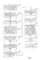
- FIG. 8 shows a flowchart illustrating a method of manufacturing a chip package (e.g. the chip package of FIG. 6 and FIG. 7 ) according to another embodiment.
- a first chip is attached on a die pad of a leadframe, wherein the leadframe includes the die pad and a plurality of lead fingers.
- a second chip is attached on the die pad, wherein the second chip may be spaced from the first chip.
- the first chip and the second chip may be attached on the die pad via die bonding using printable pastes, glue or die attach films. In another embodiment, the first chip and the second chip may be attached on the die pad using diffusion soldering. In an embodiment, the first chip and the second chip may be attached to the die pad using non-conductive die attach material, e.g. in a glue process, a die attach process or a wafer back coating process. In another embodiment, the first chip and the second chip may be attached to the die pad using conductive die attach material (such as solder paste, glue or epoxy) in a die attach process or a wafer back coating process. In a further embodiment, the first chip and the second chip may be attached to the die pad using solder wire in a soft solder process. Other suitable die attach materials and processes may also be used to attach the first chip and the second chip on the die pad in other embodiments. The attachment of the first chip and the second chip in 801 , 803 may be performed simultaneously or sequentially.
- a third chip is attached on the first chip.
- the third chip may be attached via die bonding using printable pastes, glue or die attach films, or may be attached using diffusion soldering, or using other suitable die attach materials and processes.
- the third chip may be attached on the first chip using non-conductive die attach material, e.g. in a glue/epoxy process, a die attach process or a wafer back coating process.
- the third chip may be attached to the first chip using conductive die attach material (such as solder paste, glue or epoxy) in a die attach process or a wafer back coating process.
- a clip is attached on the second chip, e.g. using solder paste or other suitable adhesive.
- the clip may be attached on the second chip using non-conductive die attach material, e.g. in a glue process, a die attach process or a wafer back coating process.
- the clip may be attached to the second chip using conductive die attach material (such as solder paste, glue or epoxy) in a die attach process or a wafer back coating process.
- the clip may be attached to the second chip using solder wire in a soft solder process.
- the clip may be attached using other suitable adhesive in other suitable process.
- the clip may be arranged such that one end of the clip is attached on the second chip and the other end of the clip is attached on one or more lead fingers.
- the clip may have a hook shape or other suitable shapes to be fit between the second chip and the corresponding lead fingers of the leadframe.
- a first set of wire bonds are formed for bonding the first chip to one or more of the lead fingers.
- a second set of wire bonds are formed for bonding the second chip to one or more of the lead fingers.
- a third set of wire bonds are formed for bonding the third chip to one or more of the lead fingers.
- the first set of wire bonds, the second set of wire bonds and the third set of wire bonds may be formed in a wire bonding process, e.g. using ball stitch on ball (BSOB) bonding.
- BSOB ball stitch on ball
- forming the first set of wire bonds, the second set of wire bonds and the third set of wire bonds may include forming one or more security bonds on the lead fingers, such that the first chip, the second chip and the third chip may be wire bonded with the respective security bonds on the respective lead fingers via the first set of wire bonds, the second set of wire bonds and the third set of wire bonds, respectively.
- the first set of wire bonds, the second set of wire bonds and the third set of wire bonds may be formed using other suitable wire bonding techniques, e.g. using solder bond, aluminum wire bond, gold wire bond, palladium coated gold wire bond, silver wire bond, or copper wire bond by thermosonic bonding or laser bonding.
- the forming of the first set of wire bonds, the second set of wire bonds and the third set of wire bonds in the wire bonding process of 809 , 811 , 813 may be carried out simultaneously or sequentially.
- a fourth chip is bonded to one or more of the lead fingers via a flip chip process.
- an active surface of the fourth chip may face an active surface of the third chip.
- the fourth chip may be bonded on the BSOB or security bonds on the lead fingers.
- a heat slug is attached on the fourth chip.
- the heat slug may be attached on the fourth chip using die attach films or diffusion solder.
- an encapsulation layer may be deposited to encapsulate the die pad, the first chip, the second chip, the third chip, the fourth chip, the first set of wire bonds, the second set of wire bonds and the third set of wire bonds.
- a lead finish may be carried out, e.g. using a coating process or a plating process.
- a trim, form and singulation process may be carried out, so as to separate individual chip packages from the leadframe.
- the various embodiments provide a single and compact chip package having multi-functionality in a miniature IC package.
- the multi-function chip package of various embodiments also provides higher electrical performance and good thermal cooling performance.
Abstract
Description
Claims (20)
Priority Applications (4)
| Application Number | Priority Date | Filing Date | Title |
|---|---|---|---|
| US13/541,789 US8759956B2 (en) | 2012-07-05 | 2012-07-05 | Chip package and method of manufacturing the same |
| DE102013106936.3A DE102013106936B4 (en) | 2012-07-05 | 2013-07-02 | Chip component and process for its manufacture |
| CN201310280959.0A CN103531561A (en) | 2012-07-05 | 2013-07-05 | Chip package and method of manufacturing the same |
| US14/306,243 US9698086B2 (en) | 2012-07-05 | 2014-06-17 | Chip package and method of manufacturing the same |
Applications Claiming Priority (1)
| Application Number | Priority Date | Filing Date | Title |
|---|---|---|---|
| US13/541,789 US8759956B2 (en) | 2012-07-05 | 2012-07-05 | Chip package and method of manufacturing the same |
Related Child Applications (1)
| Application Number | Title | Priority Date | Filing Date |
|---|---|---|---|
| US14/306,243 Continuation US9698086B2 (en) | 2012-07-05 | 2014-06-17 | Chip package and method of manufacturing the same |
Publications (2)
| Publication Number | Publication Date |
|---|---|
| US20140008776A1 US20140008776A1 (en) | 2014-01-09 |
| US8759956B2 true US8759956B2 (en) | 2014-06-24 |
Family
ID=49780791
Family Applications (2)
| Application Number | Title | Priority Date | Filing Date |
|---|---|---|---|
| US13/541,789 Active US8759956B2 (en) | 2012-07-05 | 2012-07-05 | Chip package and method of manufacturing the same |
| US14/306,243 Active US9698086B2 (en) | 2012-07-05 | 2014-06-17 | Chip package and method of manufacturing the same |
Family Applications After (1)
| Application Number | Title | Priority Date | Filing Date |
|---|---|---|---|
| US14/306,243 Active US9698086B2 (en) | 2012-07-05 | 2014-06-17 | Chip package and method of manufacturing the same |
Country Status (3)
| Country | Link |
|---|---|
| US (2) | US8759956B2 (en) |
| CN (1) | CN103531561A (en) |
| DE (1) | DE102013106936B4 (en) |
Cited By (6)
| Publication number | Priority date | Publication date | Assignee | Title |
|---|---|---|---|---|
| US10741466B2 (en) | 2017-11-17 | 2020-08-11 | Infineon Technologies Ag | Formation of conductive connection tracks in package mold body using electroless plating |
| US10777536B2 (en) | 2017-12-08 | 2020-09-15 | Infineon Technologies Ag | Semiconductor package with air cavity |
| US10796981B1 (en) | 2019-04-04 | 2020-10-06 | Infineon Technologies Ag | Chip to lead interconnect in encapsulant of molded semiconductor package |
| US11133281B2 (en) | 2019-04-04 | 2021-09-28 | Infineon Technologies Ag | Chip to chip interconnect in encapsulant of molded semiconductor package |
| US11289436B2 (en) | 2019-05-31 | 2022-03-29 | Infineon Technologies Austria Ag | Semiconductor package having a laser-activatable mold compound |
| US11587800B2 (en) | 2020-05-22 | 2023-02-21 | Infineon Technologies Ag | Semiconductor package with lead tip inspection feature |
Families Citing this family (7)
| Publication number | Priority date | Publication date | Assignee | Title |
|---|---|---|---|---|
| US9497570B2 (en) | 2014-02-06 | 2016-11-15 | Nimbelink Corp. | Embedded wireless modem |
| USD731491S1 (en) * | 2014-02-07 | 2015-06-09 | NimbeLink L.L.C. | Embedded cellular modem |
| US9802813B2 (en) * | 2014-12-24 | 2017-10-31 | Stmicroelectronics (Malta) Ltd | Wafer level package for a MEMS sensor device and corresponding manufacturing process |
| CN105227129B (en) * | 2015-09-22 | 2017-11-28 | 常州星海电子股份有限公司 | High heat conduction paster bypass diode |
| JP6695156B2 (en) * | 2016-02-02 | 2020-05-20 | エイブリック株式会社 | Resin-sealed semiconductor device |
| US20180278011A1 (en) | 2017-03-23 | 2018-09-27 | Infineon Technologies Ag | Laser diode module |
| JP2022076308A (en) | 2020-11-09 | 2022-05-19 | 株式会社デンソー | Electric apparatus |
Citations (51)
| Publication number | Priority date | Publication date | Assignee | Title |
|---|---|---|---|---|
| US5471369A (en) * | 1993-07-09 | 1995-11-28 | Fujitsu Limited | Semiconductor device having a plurality of semiconductor chips |
| US5479051A (en) * | 1992-10-09 | 1995-12-26 | Fujitsu Limited | Semiconductor device having a plurality of semiconductor chips |
| US5488254A (en) * | 1991-08-05 | 1996-01-30 | Hitachi, Ltd. | Plastic-molded-type semiconductor device |
| US5527740A (en) | 1994-06-28 | 1996-06-18 | Intel Corporation | Manufacturing dual sided wire bonded integrated circuit chip packages using offset wire bonds and support block cavities |
| US5705851A (en) * | 1995-06-28 | 1998-01-06 | National Semiconductor Corporation | Thermal ball lead integrated package |
| US5814881A (en) * | 1996-12-20 | 1998-09-29 | Lsi Logic Corporation | Stacked integrated chip package and method of making same |
| US6037661A (en) * | 1996-12-20 | 2000-03-14 | International Business Machines | Multichip module |
| US6069025A (en) * | 1994-11-15 | 2000-05-30 | Lg Semicon Co., Ltd. | Method for packaging a semiconductor device |
| US6080264A (en) * | 1996-05-20 | 2000-06-27 | Micron Technology, Inc. | Combination of semiconductor interconnect |
| US6316822B1 (en) * | 1998-09-16 | 2001-11-13 | Texas Instruments Incorporated | Multichip assembly semiconductor |
| US20020041027A1 (en) * | 2000-10-10 | 2002-04-11 | Kabushiki Kaisha Toshiba | Semiconductor device |
| US6414385B1 (en) * | 1999-11-08 | 2002-07-02 | Siliconware Precisionindustries Co., Ltd. | Quad flat non-lead package of semiconductor |
| US6426559B1 (en) * | 2000-06-29 | 2002-07-30 | National Semiconductor Corporation | Miniature 3D multi-chip module |
| US6437447B1 (en) | 2000-09-06 | 2002-08-20 | Siliconware Precision Industries Co., Ltd. | Dual-sided chip package without a die pad |
| US20020130397A1 (en) * | 1998-09-28 | 2002-09-19 | Chee Kiang Yew | Direct attachment semiconductor chip to organic substrate |
| US6483181B2 (en) * | 2001-04-19 | 2002-11-19 | Walton Advanced Electronics Ltd. | Multi-chip package |
| US20030001252A1 (en) * | 2000-03-25 | 2003-01-02 | Ku Jae Hun | Semiconductor package including stacked chips |
| US20030006501A1 (en) * | 2000-03-09 | 2003-01-09 | Fujitsu Limited | Semiconductor device, method of manufacturing semiconductor device, lead frame, method of manufacturing lead frame, and method of manufacturing semiconductor device with lead frame |
| US6552419B2 (en) * | 2001-01-25 | 2003-04-22 | Sharp Kabushiki Kaisha | Semiconductor device and liquid crystal module using the same |
| US6590281B2 (en) * | 2001-11-15 | 2003-07-08 | Siliconware Precision Industries Co., Ltd. | Crack-preventive semiconductor package |
| US6690089B2 (en) * | 2002-05-15 | 2004-02-10 | Oki Electric Industry Co., Ltd. | Semiconductor device having multi-chip package |
| US6815255B2 (en) * | 2001-08-08 | 2004-11-09 | Matsushita Electric Industrial Co., Ltd. | Semiconductor device and manufacturing method thereof |
| US20050051875A1 (en) * | 2003-09-05 | 2005-03-10 | Sunji Ichikawa | Lead frame, manufacturing method of the same, and semiconductor device using the same |
| US6951982B2 (en) * | 2002-11-22 | 2005-10-04 | Micron Technology, Inc. | Packaged microelectronic component assemblies |
| US6963141B2 (en) * | 1999-12-31 | 2005-11-08 | Jung-Yu Lee | Semiconductor package for efficient heat spreading |
| US20060091516A1 (en) * | 2004-11-01 | 2006-05-04 | Akira Matsunami | Flexible leaded stacked semiconductor package |
| US20060180904A1 (en) * | 2005-02-14 | 2006-08-17 | Stats Chippac Ltd. | Non-leaded integrated circuit package system |
| US20070164409A1 (en) * | 2003-12-18 | 2007-07-19 | Andrew Holland | Semiconductor package with integrated heatsink and electromagnetic shield |
| US7253508B2 (en) * | 2003-12-19 | 2007-08-07 | Advanced Semiconductor Engineering, Inc. | Semiconductor package with a flip chip on a solder-resist leadframe |
| US20070200248A1 (en) * | 2006-02-27 | 2007-08-30 | Stats Chippac Ltd. | Stacked integrated circuit package system |
| US7309923B2 (en) * | 2003-06-16 | 2007-12-18 | Sandisk Corporation | Integrated circuit package having stacked integrated circuits and method therefor |
| US7361986B2 (en) * | 2004-12-01 | 2008-04-22 | Taiwan Semiconductor Manufacturing Company, Ltd. | Heat stud for stacked chip package |
| US7436048B2 (en) * | 2004-10-18 | 2008-10-14 | Chippac, Inc. | Multichip leadframe package |
| US20090051027A1 (en) * | 2000-03-13 | 2009-02-26 | Megica Corporation | Method of Manufacture and Identification of Semiconductor Chip Marked For Identification with Internal Marking Indicia and Protection Thereof by Non-black Layer and Device Produced Thereby |
| US20090096115A1 (en) * | 2006-06-13 | 2009-04-16 | Siliconware Precision Industries Co., Ltd. | Semiconductor package and method for fabricating the same |
| US20090115037A1 (en) * | 2007-11-01 | 2009-05-07 | National Semiconductor Corporation | Integrated circuit package with integrated heat sink |
| US20090127680A1 (en) * | 2007-11-16 | 2009-05-21 | Byung Tai Do | Integrated circuit package-in-package system with wire-in-film encapsulant |
| US7598603B2 (en) * | 2006-03-15 | 2009-10-06 | Infineon Technologies Ag | Electronic component having a power switch with an anode thereof mounted on a die attach region of a heat sink |
| US7608915B2 (en) * | 2007-05-11 | 2009-10-27 | Siliconware Precision Industries Co., Ltd. | Heat dissipation semiconductor package |
| US20090294937A1 (en) * | 2006-09-27 | 2009-12-03 | Texas Instruments Incorporated | Two-way heat extraction from packaged semiconductor chips |
| US20110147899A1 (en) * | 2007-06-21 | 2011-06-23 | Frederick Rodriguez Dahilig | Integrated circuit package system employing device stacking |
| US20110180928A1 (en) * | 2008-08-01 | 2011-07-28 | Zigmund Ramirez Camacho | Etched recess package on package system |
| USRE42653E1 (en) * | 2001-12-07 | 2011-08-30 | Siliconware Precision Industries Co., Ltd. | Semiconductor package with heat dissipating structure |
| US8022539B2 (en) * | 2008-11-17 | 2011-09-20 | Stats Chippac Ltd. | Integrated circuit packaging system with increased connectivity and method of manufacture thereof |
| US8049313B2 (en) * | 2006-09-20 | 2011-11-01 | Freescale Semiconductor, Inc. | Heat spreader for semiconductor package |
| US8062933B2 (en) * | 2004-11-16 | 2011-11-22 | Siliconware Precision Industries Co., Ltd. | Method for fabricating heat dissipating package structure |
| US8067824B2 (en) * | 2004-03-24 | 2011-11-29 | Avago Technologies Wireless Ip (Singapore) Pte. Ltd. | Integrated circuit module package and assembly method thereof |
| US8080867B2 (en) * | 2009-10-29 | 2011-12-20 | Stats Chippac Ltd. | Integrated circuit packaging system with stacked integrated circuit and method of manufacture thereof |
| US20120181677A1 (en) * | 2008-04-04 | 2012-07-19 | Gem Services, Inc. | Semiconductor device package with two component lead frame |
| US20120193772A1 (en) * | 2011-01-28 | 2012-08-02 | Hunt Hang Jiang | Stacked die packages with flip-chip and wire bonding dies |
| US8569082B2 (en) * | 2008-10-14 | 2013-10-29 | Texas Instruments Incorporated | Semiconductor package with a mold material encapsulating a chip and a portion of a lead frame |
Family Cites Families (5)
| Publication number | Priority date | Publication date | Assignee | Title |
|---|---|---|---|---|
| JP3542311B2 (en) | 2000-01-28 | 2004-07-14 | 株式会社ルネサステクノロジ | Semiconductor device |
| US7265448B2 (en) * | 2004-01-26 | 2007-09-04 | Marvell World Trade Ltd. | Interconnect structure for power transistors |
| US7663211B2 (en) | 2006-05-19 | 2010-02-16 | Fairchild Semiconductor Corporation | Dual side cooling integrated power device package and module with a clip attached to a leadframe in the package and the module and methods of manufacture |
| US7825508B2 (en) | 2006-07-28 | 2010-11-02 | Alpha Omega Semiconductor, Inc. | Multi-die DC-DC buck power converter with efficient packaging |
| US7737537B2 (en) * | 2007-12-12 | 2010-06-15 | Infineon Technologies Ag | Electronic device |
-
2012
- 2012-07-05 US US13/541,789 patent/US8759956B2/en active Active
-
2013
- 2013-07-02 DE DE102013106936.3A patent/DE102013106936B4/en active Active
- 2013-07-05 CN CN201310280959.0A patent/CN103531561A/en active Pending
-
2014
- 2014-06-17 US US14/306,243 patent/US9698086B2/en active Active
Patent Citations (59)
| Publication number | Priority date | Publication date | Assignee | Title |
|---|---|---|---|---|
| US5488254A (en) * | 1991-08-05 | 1996-01-30 | Hitachi, Ltd. | Plastic-molded-type semiconductor device |
| US5479051A (en) * | 1992-10-09 | 1995-12-26 | Fujitsu Limited | Semiconductor device having a plurality of semiconductor chips |
| US5471369A (en) * | 1993-07-09 | 1995-11-28 | Fujitsu Limited | Semiconductor device having a plurality of semiconductor chips |
| US5527740A (en) | 1994-06-28 | 1996-06-18 | Intel Corporation | Manufacturing dual sided wire bonded integrated circuit chip packages using offset wire bonds and support block cavities |
| US5545922A (en) | 1994-06-28 | 1996-08-13 | Intel Corporation | Dual sided integrated circuit chip package with offset wire bonds and support block cavities |
| US6069025A (en) * | 1994-11-15 | 2000-05-30 | Lg Semicon Co., Ltd. | Method for packaging a semiconductor device |
| US5705851A (en) * | 1995-06-28 | 1998-01-06 | National Semiconductor Corporation | Thermal ball lead integrated package |
| US6080264A (en) * | 1996-05-20 | 2000-06-27 | Micron Technology, Inc. | Combination of semiconductor interconnect |
| US5814881A (en) * | 1996-12-20 | 1998-09-29 | Lsi Logic Corporation | Stacked integrated chip package and method of making same |
| US6037661A (en) * | 1996-12-20 | 2000-03-14 | International Business Machines | Multichip module |
| US6316822B1 (en) * | 1998-09-16 | 2001-11-13 | Texas Instruments Incorporated | Multichip assembly semiconductor |
| US20020130397A1 (en) * | 1998-09-28 | 2002-09-19 | Chee Kiang Yew | Direct attachment semiconductor chip to organic substrate |
| US6414385B1 (en) * | 1999-11-08 | 2002-07-02 | Siliconware Precisionindustries Co., Ltd. | Quad flat non-lead package of semiconductor |
| US6963141B2 (en) * | 1999-12-31 | 2005-11-08 | Jung-Yu Lee | Semiconductor package for efficient heat spreading |
| US20030006501A1 (en) * | 2000-03-09 | 2003-01-09 | Fujitsu Limited | Semiconductor device, method of manufacturing semiconductor device, lead frame, method of manufacturing lead frame, and method of manufacturing semiconductor device with lead frame |
| US20090051027A1 (en) * | 2000-03-13 | 2009-02-26 | Megica Corporation | Method of Manufacture and Identification of Semiconductor Chip Marked For Identification with Internal Marking Indicia and Protection Thereof by Non-black Layer and Device Produced Thereby |
| US6759737B2 (en) * | 2000-03-25 | 2004-07-06 | Amkor Technology, Inc. | Semiconductor package including stacked chips with aligned input/output pads |
| US20030001252A1 (en) * | 2000-03-25 | 2003-01-02 | Ku Jae Hun | Semiconductor package including stacked chips |
| US6426559B1 (en) * | 2000-06-29 | 2002-07-30 | National Semiconductor Corporation | Miniature 3D multi-chip module |
| US6437447B1 (en) | 2000-09-06 | 2002-08-20 | Siliconware Precision Industries Co., Ltd. | Dual-sided chip package without a die pad |
| US20020041027A1 (en) * | 2000-10-10 | 2002-04-11 | Kabushiki Kaisha Toshiba | Semiconductor device |
| US6552419B2 (en) * | 2001-01-25 | 2003-04-22 | Sharp Kabushiki Kaisha | Semiconductor device and liquid crystal module using the same |
| US6483181B2 (en) * | 2001-04-19 | 2002-11-19 | Walton Advanced Electronics Ltd. | Multi-chip package |
| US6815255B2 (en) * | 2001-08-08 | 2004-11-09 | Matsushita Electric Industrial Co., Ltd. | Semiconductor device and manufacturing method thereof |
| US6590281B2 (en) * | 2001-11-15 | 2003-07-08 | Siliconware Precision Industries Co., Ltd. | Crack-preventive semiconductor package |
| US20030214048A1 (en) * | 2001-11-15 | 2003-11-20 | Siliconware Precision Industries Co., Ltd. | Semiconductor package and fabricating method thereof |
| US6764880B2 (en) * | 2001-11-15 | 2004-07-20 | Siliconware Precision Industries Co., Ltd. | Semiconductor package and fabricating method thereof |
| USRE42653E1 (en) * | 2001-12-07 | 2011-08-30 | Siliconware Precision Industries Co., Ltd. | Semiconductor package with heat dissipating structure |
| US6690089B2 (en) * | 2002-05-15 | 2004-02-10 | Oki Electric Industry Co., Ltd. | Semiconductor device having multi-chip package |
| US6951982B2 (en) * | 2002-11-22 | 2005-10-04 | Micron Technology, Inc. | Packaged microelectronic component assemblies |
| US7309923B2 (en) * | 2003-06-16 | 2007-12-18 | Sandisk Corporation | Integrated circuit package having stacked integrated circuits and method therefor |
| US20050051875A1 (en) * | 2003-09-05 | 2005-03-10 | Sunji Ichikawa | Lead frame, manufacturing method of the same, and semiconductor device using the same |
| US7102210B2 (en) * | 2003-09-05 | 2006-09-05 | Oki Electric Industry Co., Ltd. | Lead frame, manufacturing method of the same, and semiconductor device using the same |
| US20070164409A1 (en) * | 2003-12-18 | 2007-07-19 | Andrew Holland | Semiconductor package with integrated heatsink and electromagnetic shield |
| US7253508B2 (en) * | 2003-12-19 | 2007-08-07 | Advanced Semiconductor Engineering, Inc. | Semiconductor package with a flip chip on a solder-resist leadframe |
| US8067824B2 (en) * | 2004-03-24 | 2011-11-29 | Avago Technologies Wireless Ip (Singapore) Pte. Ltd. | Integrated circuit module package and assembly method thereof |
| US7436048B2 (en) * | 2004-10-18 | 2008-10-14 | Chippac, Inc. | Multichip leadframe package |
| US20060091516A1 (en) * | 2004-11-01 | 2006-05-04 | Akira Matsunami | Flexible leaded stacked semiconductor package |
| US8062933B2 (en) * | 2004-11-16 | 2011-11-22 | Siliconware Precision Industries Co., Ltd. | Method for fabricating heat dissipating package structure |
| US7361986B2 (en) * | 2004-12-01 | 2008-04-22 | Taiwan Semiconductor Manufacturing Company, Ltd. | Heat stud for stacked chip package |
| US8093694B2 (en) * | 2005-02-14 | 2012-01-10 | Stats Chippac Ltd. | Method of manufacturing non-leaded integrated circuit package system having etched differential height lead structures |
| US20060180904A1 (en) * | 2005-02-14 | 2006-08-17 | Stats Chippac Ltd. | Non-leaded integrated circuit package system |
| US20070200248A1 (en) * | 2006-02-27 | 2007-08-30 | Stats Chippac Ltd. | Stacked integrated circuit package system |
| US7598603B2 (en) * | 2006-03-15 | 2009-10-06 | Infineon Technologies Ag | Electronic component having a power switch with an anode thereof mounted on a die attach region of a heat sink |
| US20090096115A1 (en) * | 2006-06-13 | 2009-04-16 | Siliconware Precision Industries Co., Ltd. | Semiconductor package and method for fabricating the same |
| US8049313B2 (en) * | 2006-09-20 | 2011-11-01 | Freescale Semiconductor, Inc. | Heat spreader for semiconductor package |
| US20090294937A1 (en) * | 2006-09-27 | 2009-12-03 | Texas Instruments Incorporated | Two-way heat extraction from packaged semiconductor chips |
| US7608915B2 (en) * | 2007-05-11 | 2009-10-27 | Siliconware Precision Industries Co., Ltd. | Heat dissipation semiconductor package |
| US20110147899A1 (en) * | 2007-06-21 | 2011-06-23 | Frederick Rodriguez Dahilig | Integrated circuit package system employing device stacking |
| US8174127B2 (en) * | 2007-06-21 | 2012-05-08 | Stats Chippac Ltd. | Integrated circuit package system employing device stacking |
| US20090115037A1 (en) * | 2007-11-01 | 2009-05-07 | National Semiconductor Corporation | Integrated circuit package with integrated heat sink |
| US20090127680A1 (en) * | 2007-11-16 | 2009-05-21 | Byung Tai Do | Integrated circuit package-in-package system with wire-in-film encapsulant |
| US20120181677A1 (en) * | 2008-04-04 | 2012-07-19 | Gem Services, Inc. | Semiconductor device package with two component lead frame |
| US20110180928A1 (en) * | 2008-08-01 | 2011-07-28 | Zigmund Ramirez Camacho | Etched recess package on package system |
| US8569082B2 (en) * | 2008-10-14 | 2013-10-29 | Texas Instruments Incorporated | Semiconductor package with a mold material encapsulating a chip and a portion of a lead frame |
| US20110298113A1 (en) * | 2008-11-17 | 2011-12-08 | Frederick Rodriguez Dahilig | Integrated circuit packaging system with increased connectivity and method of manufacture thereof |
| US8022539B2 (en) * | 2008-11-17 | 2011-09-20 | Stats Chippac Ltd. | Integrated circuit packaging system with increased connectivity and method of manufacture thereof |
| US8080867B2 (en) * | 2009-10-29 | 2011-12-20 | Stats Chippac Ltd. | Integrated circuit packaging system with stacked integrated circuit and method of manufacture thereof |
| US20120193772A1 (en) * | 2011-01-28 | 2012-08-02 | Hunt Hang Jiang | Stacked die packages with flip-chip and wire bonding dies |
Cited By (8)
| Publication number | Priority date | Publication date | Assignee | Title |
|---|---|---|---|---|
| US10741466B2 (en) | 2017-11-17 | 2020-08-11 | Infineon Technologies Ag | Formation of conductive connection tracks in package mold body using electroless plating |
| US11296000B2 (en) | 2017-11-17 | 2022-04-05 | Infineon Technologies Ag | Formation of conductive connection tracks in package mold body using electroless plating |
| US10777536B2 (en) | 2017-12-08 | 2020-09-15 | Infineon Technologies Ag | Semiconductor package with air cavity |
| US10796981B1 (en) | 2019-04-04 | 2020-10-06 | Infineon Technologies Ag | Chip to lead interconnect in encapsulant of molded semiconductor package |
| US11133281B2 (en) | 2019-04-04 | 2021-09-28 | Infineon Technologies Ag | Chip to chip interconnect in encapsulant of molded semiconductor package |
| US11569196B2 (en) | 2019-04-04 | 2023-01-31 | Infineon Technologies Ag | Chip to chip interconnect in encapsulant of molded semiconductor package |
| US11289436B2 (en) | 2019-05-31 | 2022-03-29 | Infineon Technologies Austria Ag | Semiconductor package having a laser-activatable mold compound |
| US11587800B2 (en) | 2020-05-22 | 2023-02-21 | Infineon Technologies Ag | Semiconductor package with lead tip inspection feature |
Also Published As
| Publication number | Publication date |
|---|---|
| US20140008776A1 (en) | 2014-01-09 |
| DE102013106936A1 (en) | 2014-01-09 |
| US20140291823A1 (en) | 2014-10-02 |
| DE102013106936B4 (en) | 2020-08-13 |
| CN103531561A (en) | 2014-01-22 |
| US9698086B2 (en) | 2017-07-04 |
Similar Documents
| Publication | Publication Date | Title |
|---|---|---|
| US9698086B2 (en) | Chip package and method of manufacturing the same | |
| US8836101B2 (en) | Multi-chip semiconductor packages and assembly thereof | |
| US8426255B2 (en) | Chip package structure and method for manufacturing the same | |
| US8916474B2 (en) | Semiconductor modules and methods of formation thereof | |
| US7221055B2 (en) | System and method for die attach using a backside heat spreader | |
| US20110244633A1 (en) | Package assembly for semiconductor devices | |
| US20090127680A1 (en) | Integrated circuit package-in-package system with wire-in-film encapsulant | |
| US20090189261A1 (en) | Ultra-Thin Semiconductor Package | |
| US9478484B2 (en) | Semiconductor packages and methods of formation thereof | |
| US9984897B2 (en) | Method for manufacturing a chip arrangement including a ceramic layer | |
| JP2007088453A (en) | Method of manufacturing stack die package | |
| US20070035019A1 (en) | Semiconductor component and method of manufacture | |
| EP2287898A2 (en) | Shrink Package on Board | |
| US10217698B2 (en) | Die attachment for packaged semiconductor device | |
| US20150060878A1 (en) | Semiconductor Packages Having Multiple Lead Frames and Methods of Formation Thereof | |
| US20020053736A1 (en) | Semiconductor package | |
| US10522448B2 (en) | Single or multi chip module package and related methods | |
| US20110163428A1 (en) | Semiconductor packages with embedded heat sink | |
| US9852961B2 (en) | Packaged semiconductor device having an encapsulated semiconductor chip | |
| US10242927B2 (en) | Semiconductor package, semiconductor device using the same and manufacturing method thereof | |
| US20240014123A1 (en) | Semiconductor device with lead-on-chip interconnect and method therefor | |
| KR20040060123A (en) | Method for packaging semiconductor device | |
| TW202236540A (en) | Semiconductor manufacturing device and method of enhancing mold gate injector and air vent to reduce voids in encapsulant | |
| US20140339690A1 (en) | Elimination of Die-Top Delamination |
Legal Events
| Date | Code | Title | Description |
|---|---|---|---|
| AS | Assignment |
Owner name: INFINEON TECHNOLOGIES AG, GERMANY Free format text: ASSIGNMENT OF ASSIGNORS INTEREST;ASSIGNOR:SOLLER, TYRONE JON DONATO;REEL/FRAME:028490/0147 Effective date: 20120704 |
|
| FEPP | Fee payment procedure |
Free format text: PAYOR NUMBER ASSIGNED (ORIGINAL EVENT CODE: ASPN); ENTITY STATUS OF PATENT OWNER: LARGE ENTITY |
|
| STCF | Information on status: patent grant |
Free format text: PATENTED CASE |
|
| MAFP | Maintenance fee payment |
Free format text: PAYMENT OF MAINTENANCE FEE, 4TH YEAR, LARGE ENTITY (ORIGINAL EVENT CODE: M1551) Year of fee payment: 4 |
|
| MAFP | Maintenance fee payment |
Free format text: PAYMENT OF MAINTENANCE FEE, 8TH YEAR, LARGE ENTITY (ORIGINAL EVENT CODE: M1552); ENTITY STATUS OF PATENT OWNER: LARGE ENTITY Year of fee payment: 8 |