US8723392B2 - Saw filter having planar barrier layer and method of making - Google Patents
Saw filter having planar barrier layer and method of making Download PDFInfo
- Publication number
- US8723392B2 US8723392B2 US13/183,977 US201113183977A US8723392B2 US 8723392 B2 US8723392 B2 US 8723392B2 US 201113183977 A US201113183977 A US 201113183977A US 8723392 B2 US8723392 B2 US 8723392B2
- Authority
- US
- United States
- Prior art keywords
- barrier layer
- metal
- piezoelectric substrate
- layer
- planar
- Prior art date
- Legal status (The legal status is an assumption and is not a legal conclusion. Google has not performed a legal analysis and makes no representation as to the accuracy of the status listed.)
- Expired - Fee Related, expires
Links
Images


Classifications
-
- H—ELECTRICITY
- H03—ELECTRONIC CIRCUITRY
- H03H—IMPEDANCE NETWORKS, e.g. RESONANT CIRCUITS; RESONATORS
- H03H3/00—Apparatus or processes specially adapted for the manufacture of impedance networks, resonating circuits, resonators
- H03H3/007—Apparatus or processes specially adapted for the manufacture of impedance networks, resonating circuits, resonators for the manufacture of electromechanical resonators or networks
- H03H3/08—Apparatus or processes specially adapted for the manufacture of impedance networks, resonating circuits, resonators for the manufacture of electromechanical resonators or networks for the manufacture of resonators or networks using surface acoustic waves
- H03H3/10—Apparatus or processes specially adapted for the manufacture of impedance networks, resonating circuits, resonators for the manufacture of electromechanical resonators or networks for the manufacture of resonators or networks using surface acoustic waves for obtaining desired frequency or temperature coefficient
-
- H—ELECTRICITY
- H03—ELECTRONIC CIRCUITRY
- H03H—IMPEDANCE NETWORKS, e.g. RESONANT CIRCUITS; RESONATORS
- H03H9/00—Networks comprising electromechanical or electro-acoustic devices; Electromechanical resonators
- H03H9/02—Details
- H03H9/02535—Details of surface acoustic wave devices
- H03H9/02818—Means for compensation or elimination of undesirable effects
- H03H9/02834—Means for compensation or elimination of undesirable effects of temperature influence
-
- H—ELECTRICITY
- H03—ELECTRONIC CIRCUITRY
- H03H—IMPEDANCE NETWORKS, e.g. RESONANT CIRCUITS; RESONATORS
- H03H9/00—Networks comprising electromechanical or electro-acoustic devices; Electromechanical resonators
- H03H9/02—Details
- H03H9/125—Driving means, e.g. electrodes, coils
- H03H9/145—Driving means, e.g. electrodes, coils for networks using surface acoustic waves
- H03H9/14538—Formation
- H03H9/14541—Multilayer finger or busbar electrode
-
- Y—GENERAL TAGGING OF NEW TECHNOLOGICAL DEVELOPMENTS; GENERAL TAGGING OF CROSS-SECTIONAL TECHNOLOGIES SPANNING OVER SEVERAL SECTIONS OF THE IPC; TECHNICAL SUBJECTS COVERED BY FORMER USPC CROSS-REFERENCE ART COLLECTIONS [XRACs] AND DIGESTS
- Y10—TECHNICAL SUBJECTS COVERED BY FORMER USPC
- Y10T—TECHNICAL SUBJECTS COVERED BY FORMER US CLASSIFICATION
- Y10T29/00—Metal working
- Y10T29/42—Piezoelectric device making
Definitions
- This disclosure relates generally to surface acoustic wave (SAW) filters, and more particularly to SAW filter devices and a method of making the same, including a planar barrier layer.
- SAW surface acoustic wave
- SAW filters are frequently used for radio frequency (RF) filtering in devices such as wireless communication systems, due to small chip size and low insertion loss.
- RF radio frequency
- the performance of a SAW filter depends on the characteristics of the SAW propagated in a piezoelectric substrate.
- SAW filters having low temperature coefficients of frequency (TCF) result in greater temperature independence at frequencies near the center of the pass band of the device.
- Buried metal SAW filters have been used, and have demonstrated high electromagnetic coupling (high bandwidth), but may not provide a satisfactory TCF.
- Other challenges of buried metal SAW filters include damage to the piezoelectric substrate during polishing or etching steps of fabrication, and difficulty controlling thickness of buried electrodes, which in turn affects the signal frequency transmitted by the SAW filter.
- a first aspect of the disclosure provides a surface acoustic wave (SAW) filter comprising: a piezoelectric substrate; a planar barrier layer disposed above the piezoelectric substrate; and at least one metal conductor disposed in at least one trench in the planar barrier layer.
- SAW surface acoustic wave
- a second aspect of the disclosure provides a method for making a surface acoustic wave (SAW) filter, the method comprising: depositing a planar barrier layer on a piezoelectric substrate; patterning the planar barrier layer to form at least one trench; depositing a metal layer above the planar barrier layer; and polishing the metal layer to form at least one metal conductor.
- SAW surface acoustic wave
- a third aspect of the disclosure provides a surface acoustic wave (SAW) filter comprising: a piezoelectric substrate; an SiO 2 planar barrier layer disposed above the piezoelectric substrate; at least one Cu conductor buried in the planar barrier layer and the piezoelectric substrate; a diffusion barrier layer disposed above each of the at least one Cu conductors; at least one Al conductor disposed above the diffusion barrier layer; and a second SiO 2 layer disposed above the SiO 2 the planar barrier layer and the at least one Al conductor.
- SAW surface acoustic wave
- FIGS. 1-4 show an embodiment of a SAW filter structure and process for making the same.
- FIGS. 5-8 show an embodiment of a SAW filter structure having a diffusion barrier, and process for making the same.
- FIGS. 9-12 show an embodiment of a SAW filter structure including a cap layer, and process for making the same.
- FIGS. 13-16 show an embodiment of a SAW filter structure having stacked electrodes, and process for making the same.
- FIGS. 17-20 show an embodiment of a SAW filter structure having stacked electrodes and a diffusion barrier, and process for making the same.
- FIGS. 21-25 show an embodiment of a SAW filter structure having self aligned stacked electrodes, and process for making the same.
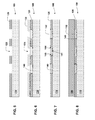
- FIGS. 1-25 show various embodiments of a SAW filter 100 , and processes for making the same.
- FIGS. 1-4 depict one embodiment of SAW filter 100 and a process for making the same.
- a piezoelectric substrate 110 is provided, which may comprise lithium niobate (LiNbO 3 ), among other piezoelectric substrates.
- a planar barrier layer 120 is provided above piezoelectric substrate 110 .
- planar barrier layer 120 may be SiO 2 , and may have a thickness of about 100 nm.
- Planar barrier layer 120 may be patterned using, e.g., lithography and etching, to form at least one trench 125 in planar barrier layer 120 .
- metal layer 130 is deposited above planar barrier layer 120 and piezoelectric substrate 110 .
- metal layer 130 may be copper (Cu), and may be deposited by, e.g., physical vapor deposition (PVD).
- PVD physical vapor deposition
- metal layer 130 may be polished using, e.g., chemical mechanical polishing (CMP) to form at least one metal conductor 132 .
- CMP chemical mechanical polishing
- barrier layer 120 acts as a polish stop, protecting piezoelectric substrate 110 .
- a layer of SiO 2 135 may be deposited over planar barrier layer 120 and metal conductor 130 .
- FIGS. 5-8 depict a further embodiment of SAW filter 100 .
- planar barrier layer 120 is deposited above piezoelectric substrate 110 and patterned to form trenches 125 , as discussed relative to FIG. 1 .
- a liner or diffusion barrier layer 140 is deposited above planar barrier layer 120 and piezoelectric substrate 110 by, e.g., PVD.
- the composition of diffusion barrier layer 140 may be any of TaN/Ta, TaSiN/Ta, WN/Ta, WN/Ru, or another composition.
- metal layer 130 may be deposited over diffusion barrier layer 140 .
- FIG. 5 planar barrier layer 120 is deposited above piezoelectric substrate 110 and patterned to form trenches 125 , as discussed relative to FIG. 1 .
- a liner or diffusion barrier layer 140 is deposited above planar barrier layer 120 and piezoelectric substrate 110 by, e.g., PVD.
- the composition of diffusion barrier layer 140 may be any of TaN/Ta, TaSiN/
- diffusion barrier layer 140 and metal layer 130 may be polished via, e.g., CMP to form at least one metal conductor 132 lined by diffusion barrier layer 140 .
- Diffusion barrier layer 140 lines both a horizontal surface 141 beneath metal conductor 132 as well as vertical surfaces 144 , 146 of metal conductor 132 as shown in FIG. 7 .
- a layer 135 of SiO 2 may be deposited over planar barrier layer 120 , metal conductor 132 , and diffusion barrier layer 140 .
- FIGS. 9-12 show a further embodiment of SAW filter 100 .
- planar barrier layer 120 is deposited over piezoelectric substrate 110 and patterned to form trenches 125 as discussed above.
- Planar barrier layer 120 may be SiO 2 , and may have a thickness of about 200 nm.
- Metal layer 130 is deposited over planar barrier layer 120 and piezoelectric substrate 110 by, e.g., PVD.
- Cap layer 150 which may be, e.g., SiN, may then be deposited over metal layer 130 by PVD or plasma-enhanced chemical vapor deposition (PECVD).
- PECVD plasma-enhanced chemical vapor deposition
- metal layer 130 and cap layer 150 may be polished using, e.g., CMP, using planar barrier layer 120 as a polish stop.
- metal layer 130 may be deposited such that a thickness 133 of metal layer 130 is less than a depth 134 of trench 125 , i.e., that metal layer 130 does not fill the full depth 134 of trench 125 .
- metal layer 130 and cap layer 150 may be deposited such that a collective thickness 136 of metal layer 130 and cap layer 150 may also be less than depth 134 of trench 125 , i.e., that together metal layer 130 and cap layer 150 do not fill trench 125 to depth 134 as shown in FIG. 10 .
- the thickness 133 of metal layer 130 , and therefore metal conductor 132 which is recessed in FIGS. 10-12 , may be controlled by adjusting the deposition of metal layer 130 rather than by polishing as in the embodiments of FIGS. 3 and 7 .
- cap layer 150 may be removed by etching, although in other embodiments it may not be removed.
- layer 135 of SiO 2 may be deposited over planar barrier layer 120 , metal conductor 132 , and, if present, cap layer 150 (not shown in FIG. 12 ).
- FIGS. 13-16 show a further embodiment of SAW filter 100 .
- planar barrier layer 120 is deposited over piezoelectric substrate 110 and patterned to form trenches 125 .
- planar barrier layer 120 may be SiO 2 .
- Metal conductors 132 are formed by depositing metal, which may be copper, over filter structure 100 , and polishing the metal using planar barrier layer 120 as a polish stop. Metal conductors 132 are thus buried in piezoelectric substrate 110 and planar barrier layer 120 as shown in FIG. 13 .
- a diffusion barrier layer 140 is deposited over metal conductors 132 .
- Diffusion barrier layer 140 may be, e.g., tantalum nitride (TaN).
- a second metal layer 160 which may be aluminum (Al), is then deposited above diffusion barrier layer 140 .
- Second metal layer 160 is then etched using, e.g., reactive ion etching using planar barrier layer 120 as an etch stop to protect piezoelectric substrate 110 .
- Second metal layer 160 may be self-aligned such that it is substantially horizontally aligned with diffusion barrier layer 140 , as shown in FIGS. 14-16 . In FIG.
- planar barrier layer 120 may then be removed by etching, although in other embodiments it may remain in place.
- metal conductor 132 , diffusion barrier layer 140 , and second metal layer 160 form stacked metal electrode 170 , which may provide high bandwidth/electromagnetic coupling, and a temperature coefficient of frequency of about 0.1.
- layer 135 of SiO 2 may be deposited over piezoelectric substrate 110 , planar barrier layer 120 if present, and stacked metal electrode 170 .
- FIGS. 17-20 show a further embodiment.
- planar barrier layer 120 is deposited over piezoelectric substrate 110 and patterned to form trenches 125 .
- planar barrier layer 120 may be SiO 2 .
- Metal conductors 132 are formed by depositing metal, which may be copper, over filter structure 100 , and polishing the metal using planar barrier layer 120 as a polish stop to protect piezoelectric substrate 110 .
- Metal conductors 132 are thus buried in piezoelectric substrate 110 and planar barrier layer 120 as shown in FIG. 17 .
- Diffusion barrier layer 142 is deposited over metal conductors 132 in a self aligned process such that metal conductor 132 and diffusion barrier layer 142 are substantially horizontally aligned.
- Diffusion barrier 142 may be, e.g., cobalt tungsten phosphate (CoWP).
- second metal layer 160 which may be aluminum (Al), is then deposited above diffusion barrier layer 142 .
- Second metal layer 160 is then etched using, e.g., reactive ion etching using planar barrier layer 120 as an etch stop.
- planar barrier layer 120 may then be removed by etching, although in other embodiments it may remain in place.
- metal conductor 132 , diffusion barrier 142 , and second metal layer 160 form stacked metal electrode 170 , which may provide high bandwidth/electromagnetic coupling, and a temperature coefficient of frequency of about 0.1.
- a layer 135 of SiO 2 may be deposited over piezoelectric substrate 110 , planar barrier layer 120 if present, and stacked metal electrode 170 .
- FIGS. 21-24 show a further embodiment including damascene stacked metal electrodes.
- planar barrier layer 120 which may be SiO 2
- trenches 125 are patterned as discussed above.
- Metal layer 130 is then deposited over planar barrier layer 120 and trenches 125 by e.g., PVD, followed by deposition of diffusion barrier layer 140 , which may be, e.g., TaN.
- SAW filter 100 is then polished as shown in FIG. 22 , resulting in metal conductors 132 which include metal lining both of the horizontal 151 and vertical 164 , 166 surfaces of trench 125 , and diffusion barrier lining both of the horizontal and vertical surfaces of metal conductor 132 .
- a recessed etch of metal layer 130 may be performed to form recessed conductors 132 .
- second metal layer 160 which may be aluminum (Al), may then be deposited and polished, forming self-aligned stacked metal electrodes 170 having a damascene configuration.
- second metal layer 160 may be deposited to a thickness equal to or greater than a depth 175 of lined trench 126 .
- the configuration of FIG. 23 may be achieved by polishing second metal layer 160 to the desired depth.
- second metal layer 160 may be deposited such that a collective thickness of metal conductor 132 , diffusion barrier layer 140 , and second metal layer 160 is less than or equal to a depth of trench 125 , as shown in FIG. 24 .
- the thickness of second metal layer 160 , and therefore stacked metal 170 may be controlled by adjusting the deposition of second metal layer 160 rather than by polishing, and may further be recessed in some embodiments as shown in FIG. 24 .
- planar barrier layer 120 may be removed.
Abstract
Description
Claims (13)
Priority Applications (6)
| Application Number | Priority Date | Filing Date | Title |
|---|---|---|---|
| US13/183,977 US8723392B2 (en) | 2011-07-15 | 2011-07-15 | Saw filter having planar barrier layer and method of making |
| GB1402779.1A GB2507693A (en) | 2011-07-15 | 2012-06-29 | Saw filter having planar barrier layer and method of making |
| DE112012002979.8T DE112012002979B4 (en) | 2011-07-15 | 2012-06-29 | Saw filter with even barrier layer and manufacturing process |
| CN201280035023.5A CN103650344B (en) | 2011-07-15 | 2012-06-29 | There is SAW wave filter and the manufacture method thereof of plane barrier layer |
| PCT/US2012/044908 WO2013012544A1 (en) | 2011-07-15 | 2012-06-29 | Saw filter having planar barrier layer and method of making |
| US13/775,338 US20130161283A1 (en) | 2011-07-15 | 2013-02-25 | Saw filter having planar barrier layer and method of making |
Applications Claiming Priority (1)
| Application Number | Priority Date | Filing Date | Title |
|---|---|---|---|
| US13/183,977 US8723392B2 (en) | 2011-07-15 | 2011-07-15 | Saw filter having planar barrier layer and method of making |
Related Child Applications (1)
| Application Number | Title | Priority Date | Filing Date |
|---|---|---|---|
| US13/775,338 Division US20130161283A1 (en) | 2011-07-15 | 2013-02-25 | Saw filter having planar barrier layer and method of making |
Publications (2)
| Publication Number | Publication Date |
|---|---|
| US20130015744A1 US20130015744A1 (en) | 2013-01-17 |
| US8723392B2 true US8723392B2 (en) | 2014-05-13 |
Family
ID=47518542
Family Applications (2)
| Application Number | Title | Priority Date | Filing Date |
|---|---|---|---|
| US13/183,977 Expired - Fee Related US8723392B2 (en) | 2011-07-15 | 2011-07-15 | Saw filter having planar barrier layer and method of making |
| US13/775,338 Abandoned US20130161283A1 (en) | 2011-07-15 | 2013-02-25 | Saw filter having planar barrier layer and method of making |
Family Applications After (1)
| Application Number | Title | Priority Date | Filing Date |
|---|---|---|---|
| US13/775,338 Abandoned US20130161283A1 (en) | 2011-07-15 | 2013-02-25 | Saw filter having planar barrier layer and method of making |
Country Status (5)
| Country | Link |
|---|---|
| US (2) | US8723392B2 (en) |
| CN (1) | CN103650344B (en) |
| DE (1) | DE112012002979B4 (en) |
| GB (1) | GB2507693A (en) |
| WO (1) | WO2013012544A1 (en) |
Families Citing this family (8)
| Publication number | Priority date | Publication date | Assignee | Title |
|---|---|---|---|---|
| US8896188B2 (en) * | 2012-04-11 | 2014-11-25 | Sand 9, Inc. | Resonator electrodes and related methods and apparatus |
| CN104009732B (en) * | 2014-06-23 | 2019-01-08 | 南通大学 | Artificial adjustable surface acoustic wave filter structure |
| JP6567661B2 (en) * | 2014-10-03 | 2019-08-28 | テクノロギアン トゥトキムスケスクス ヴェーテーテー オイ | Temperature compensated plate resonator |
| WO2017013946A1 (en) * | 2015-07-17 | 2017-01-26 | 株式会社村田製作所 | Elastic wave device |
| WO2018011697A1 (en) * | 2016-07-11 | 2018-01-18 | Epitronic Holdings Pte. Ltd. | Surface acoustic wave rfid sensor for hemodynamic wearables |
| CN112491380B (en) * | 2020-11-23 | 2023-10-20 | 广东广纳芯科技有限公司 | Method for manufacturing metal electrode of TC-SAW |
| CN112436816B (en) * | 2020-12-03 | 2024-04-09 | 广东广纳芯科技有限公司 | Temperature-compensated surface acoustic wave device and method of manufacturing the same |
| US20230223918A1 (en) * | 2022-01-13 | 2023-07-13 | RF360 Europe GmbH | Surface acoustic wave (saw) device with one or more intermediate layers for self-heating improvement |
Citations (28)
| Publication number | Priority date | Publication date | Assignee | Title |
|---|---|---|---|---|
| US4237433A (en) * | 1979-03-13 | 1980-12-02 | Sperry Corporation | Surface acoustic wave resonators with integrated internal coupler reflectors |
| US4879487A (en) * | 1987-05-26 | 1989-11-07 | Clarion Co., Ltd. | Surface-acoustic-wave device |
| US5343107A (en) | 1992-09-11 | 1994-08-30 | Sumitomo Electric Industries, Ltd. | Surface acoustic wave element and method of manufacturing the same |
| US5654127A (en) * | 1988-05-16 | 1997-08-05 | Elm Technology Corporation | Method of making a tester surface with high density probe points |
| US6004188A (en) | 1998-09-10 | 1999-12-21 | Chartered Semiconductor Manufacturing Ltd. | Method for forming copper damascene structures by using a dual CMP barrier layer |
| US6205658B1 (en) | 1998-11-26 | 2001-03-27 | Nec Corporation | Method for formation of metal wiring |
| US6376353B1 (en) | 2000-07-03 | 2002-04-23 | Chartered Semiconductor Manufacturing Ltd. | Aluminum and copper bimetallic bond pad scheme for copper damascene interconnects |
| US20020079987A1 (en) | 2000-12-21 | 2002-06-27 | Yip David S. | Recessed reflector single phase unidirectional transducer |
| US6555946B1 (en) | 2000-07-24 | 2003-04-29 | Motorola, Inc. | Acoustic wave device and process for forming the same |
| US20040076081A1 (en) * | 2001-02-16 | 2004-04-22 | Siegfried Menzel | Acoustic surface wave component |
| US6806796B2 (en) * | 2001-08-14 | 2004-10-19 | Murata Manfacturing Co., Ltd. | End-surface reflection type surface acoustic wave filter |
| US20040251792A1 (en) | 2003-05-26 | 2004-12-16 | Fujitsu Media Devices Limited & Fujitsu Limited | Surface acoustic wave element, and surface acoustic wave device including the same |
| US20060134834A1 (en) | 2001-11-16 | 2006-06-22 | Tdk Corporation | Packaging substrate and manufacturing method thereof, integrated circuit device and manufacturing method thereof, and SAW device |
| US7213314B2 (en) | 2002-07-03 | 2007-05-08 | Triquint, Inc. | Method of forming a surface acoustic wave (SAW) filter device |
| US20070120216A1 (en) | 2005-11-30 | 2007-05-31 | International Business Machines Corporation | Low cost bonding pad and method of fabricating same |
| US7259032B2 (en) | 2002-11-26 | 2007-08-21 | Murata Manufacturing Co., Ltd. | Hermetically sealing a package to include a barrier metal |
| US20070224706A1 (en) | 2006-03-27 | 2007-09-27 | Fujitsu Limited | Method of producing semiconductor device and semiconductor device |
| US7385334B1 (en) * | 2006-11-20 | 2008-06-10 | Sandia Corporation | Contour mode resonators with acoustic reflectors |
| US7446453B1 (en) | 2006-07-05 | 2008-11-04 | Triquint, Inc. | Surface acoustic wave devices using surface acoustic waves with strong piezoelectric coupling |
| US20090021109A1 (en) | 2005-03-22 | 2009-01-22 | Matsushita Electric Industrial Co., Ltd. | Under bump metal film, method for forming same, and surface acoustic wave device |
| US7629866B2 (en) | 2006-01-11 | 2009-12-08 | Murata Manufacturing Co., Ltd. | Method for manufacturing surface acoustic wave device and surface acoustic wave device |
| US20100019386A1 (en) | 2008-07-25 | 2010-01-28 | Oh Joon Seok | Electrical conductor line having a multilayer diffusion barrier for use in a semiconductor device and method for forming the same |
| US7723227B1 (en) | 2009-03-24 | 2010-05-25 | Micron Technology, Inc. | Methods of forming copper-comprising conductive lines in the fabrication of integrated circuitry |
| US20100244624A1 (en) | 2009-03-25 | 2010-09-30 | Fujitsu Limited | Acoustic wave device and method of producing the same |
| US20100320866A1 (en) * | 2006-10-12 | 2010-12-23 | Murata Manufacturing Co., Ltd. | Boundary acoustic wave device |
| US20110012695A1 (en) | 2009-07-15 | 2011-01-20 | Panasonic Corporation | Acoustic wave device and electronic apparatus using the same |
| US7915786B2 (en) | 2007-08-14 | 2011-03-29 | Taiyo Yuden Co., Ltd. | Elastic boundary wave device |
| US8344589B2 (en) * | 2009-08-10 | 2013-01-01 | Murata Manufacturing Co., Ltd. | Boundary acoustic wave device |
Family Cites Families (6)
| Publication number | Priority date | Publication date | Assignee | Title |
|---|---|---|---|---|
| US6359328B1 (en) * | 1998-12-31 | 2002-03-19 | Intel Corporation | Methods for making interconnects and diffusion barriers in integrated circuits |
| DE10216559B4 (en) * | 2002-04-09 | 2007-08-09 | Leibniz-Institut für Festkörper- und Werkstoffforschung e.V. | Acoustic surface acoustic wave device and method for its production |
| JP3841053B2 (en) * | 2002-07-24 | 2006-11-01 | 株式会社村田製作所 | Surface acoustic wave device and manufacturing method thereof |
| US7193323B2 (en) * | 2003-11-18 | 2007-03-20 | International Business Machines Corporation | Electroplated CoWP composite structures as copper barrier layers |
| WO2005083881A1 (en) * | 2004-03-02 | 2005-09-09 | Murata Manufacturing Co., Ltd. | Surface acoustic wave device |
| JP2006005190A (en) * | 2004-06-18 | 2006-01-05 | Renesas Technology Corp | Semiconductor device |
-
2011
- 2011-07-15 US US13/183,977 patent/US8723392B2/en not_active Expired - Fee Related
-
2012
- 2012-06-29 WO PCT/US2012/044908 patent/WO2013012544A1/en active Application Filing
- 2012-06-29 DE DE112012002979.8T patent/DE112012002979B4/en not_active Expired - Fee Related
- 2012-06-29 GB GB1402779.1A patent/GB2507693A/en not_active Withdrawn
- 2012-06-29 CN CN201280035023.5A patent/CN103650344B/en not_active Expired - Fee Related
-
2013
- 2013-02-25 US US13/775,338 patent/US20130161283A1/en not_active Abandoned
Patent Citations (29)
| Publication number | Priority date | Publication date | Assignee | Title |
|---|---|---|---|---|
| US4237433A (en) * | 1979-03-13 | 1980-12-02 | Sperry Corporation | Surface acoustic wave resonators with integrated internal coupler reflectors |
| US4879487A (en) * | 1987-05-26 | 1989-11-07 | Clarion Co., Ltd. | Surface-acoustic-wave device |
| US5654127A (en) * | 1988-05-16 | 1997-08-05 | Elm Technology Corporation | Method of making a tester surface with high density probe points |
| US5343107A (en) | 1992-09-11 | 1994-08-30 | Sumitomo Electric Industries, Ltd. | Surface acoustic wave element and method of manufacturing the same |
| US6004188A (en) | 1998-09-10 | 1999-12-21 | Chartered Semiconductor Manufacturing Ltd. | Method for forming copper damascene structures by using a dual CMP barrier layer |
| US6205658B1 (en) | 1998-11-26 | 2001-03-27 | Nec Corporation | Method for formation of metal wiring |
| US6376353B1 (en) | 2000-07-03 | 2002-04-23 | Chartered Semiconductor Manufacturing Ltd. | Aluminum and copper bimetallic bond pad scheme for copper damascene interconnects |
| US6555946B1 (en) | 2000-07-24 | 2003-04-29 | Motorola, Inc. | Acoustic wave device and process for forming the same |
| US20020079987A1 (en) | 2000-12-21 | 2002-06-27 | Yip David S. | Recessed reflector single phase unidirectional transducer |
| US20040076081A1 (en) * | 2001-02-16 | 2004-04-22 | Siegfried Menzel | Acoustic surface wave component |
| US6853115B2 (en) | 2001-02-16 | 2005-02-08 | Leibniz-Institut Fuer Festkoerper-Und Werkstoffforschung Dresden E.V. | Acoustic surface wave component |
| US6806796B2 (en) * | 2001-08-14 | 2004-10-19 | Murata Manfacturing Co., Ltd. | End-surface reflection type surface acoustic wave filter |
| US20060134834A1 (en) | 2001-11-16 | 2006-06-22 | Tdk Corporation | Packaging substrate and manufacturing method thereof, integrated circuit device and manufacturing method thereof, and SAW device |
| US7213314B2 (en) | 2002-07-03 | 2007-05-08 | Triquint, Inc. | Method of forming a surface acoustic wave (SAW) filter device |
| US7259032B2 (en) | 2002-11-26 | 2007-08-21 | Murata Manufacturing Co., Ltd. | Hermetically sealing a package to include a barrier metal |
| US20040251792A1 (en) | 2003-05-26 | 2004-12-16 | Fujitsu Media Devices Limited & Fujitsu Limited | Surface acoustic wave element, and surface acoustic wave device including the same |
| US20090021109A1 (en) | 2005-03-22 | 2009-01-22 | Matsushita Electric Industrial Co., Ltd. | Under bump metal film, method for forming same, and surface acoustic wave device |
| US20070120216A1 (en) | 2005-11-30 | 2007-05-31 | International Business Machines Corporation | Low cost bonding pad and method of fabricating same |
| US7629866B2 (en) | 2006-01-11 | 2009-12-08 | Murata Manufacturing Co., Ltd. | Method for manufacturing surface acoustic wave device and surface acoustic wave device |
| US20070224706A1 (en) | 2006-03-27 | 2007-09-27 | Fujitsu Limited | Method of producing semiconductor device and semiconductor device |
| US7446453B1 (en) | 2006-07-05 | 2008-11-04 | Triquint, Inc. | Surface acoustic wave devices using surface acoustic waves with strong piezoelectric coupling |
| US20100320866A1 (en) * | 2006-10-12 | 2010-12-23 | Murata Manufacturing Co., Ltd. | Boundary acoustic wave device |
| US7385334B1 (en) * | 2006-11-20 | 2008-06-10 | Sandia Corporation | Contour mode resonators with acoustic reflectors |
| US7915786B2 (en) | 2007-08-14 | 2011-03-29 | Taiyo Yuden Co., Ltd. | Elastic boundary wave device |
| US20100019386A1 (en) | 2008-07-25 | 2010-01-28 | Oh Joon Seok | Electrical conductor line having a multilayer diffusion barrier for use in a semiconductor device and method for forming the same |
| US7723227B1 (en) | 2009-03-24 | 2010-05-25 | Micron Technology, Inc. | Methods of forming copper-comprising conductive lines in the fabrication of integrated circuitry |
| US20100244624A1 (en) | 2009-03-25 | 2010-09-30 | Fujitsu Limited | Acoustic wave device and method of producing the same |
| US20110012695A1 (en) | 2009-07-15 | 2011-01-20 | Panasonic Corporation | Acoustic wave device and electronic apparatus using the same |
| US8344589B2 (en) * | 2009-08-10 | 2013-01-01 | Murata Manufacturing Co., Ltd. | Boundary acoustic wave device |
Non-Patent Citations (4)
| Title |
|---|
| Kimura et al., "High Q SAW Resonator Using Upper-Electrodes on Grooved-Electrodes in LiTaO3," 2010, pp. 1740-1743, IEEE. |
| Nakai et al., "Surface Acoustic Wave Duplexer Composed of SiO2 Film with Convex and Concave on Cu-electrodes/LiNbO3 Structure," 2008, pp. 1580-1583, Digital Object Identifier: 10.1109/ULTSYM.2008.0385, IEEE International Ultrasonics Symposium Proceedings. |
| Patent Cooperation Treaty, Notification of Transmittal of the International Search Report and the Written Opinion of the International Searching Authority, or the Declaration for PCT/US2012/044908 dated Oct. 2, 2012, 11 pages. |
| Reitz et al., "Damascene Technique Applied to Surface Acoustic Wave Devices," 2007, pp. 271-276, J. Vac. Science Technology, B 25(1), American Vacuum Society. |
Also Published As
| Publication number | Publication date |
|---|---|
| US20130161283A1 (en) | 2013-06-27 |
| US20130015744A1 (en) | 2013-01-17 |
| GB201402779D0 (en) | 2014-04-02 |
| GB2507693A (en) | 2014-05-07 |
| CN103650344B (en) | 2016-05-25 |
| CN103650344A (en) | 2014-03-19 |
| DE112012002979B4 (en) | 2017-12-28 |
| DE112012002979T5 (en) | 2014-04-30 |
| WO2013012544A1 (en) | 2013-01-24 |
Similar Documents
| Publication | Publication Date | Title |
|---|---|---|
| US8723392B2 (en) | Saw filter having planar barrier layer and method of making | |
| US10354949B2 (en) | Air gap structure and method | |
| US8680682B2 (en) | Barrier for through-silicon via | |
| CN108365829A (en) | The preparation method of monocrystalline piezoelectric rf-resonator and filter | |
| US11671067B2 (en) | Piezoelectric acoustic resonator manufactured with piezoelectric thin film transfer process | |
| US10490500B2 (en) | Metal line structure and method | |
| US20070254397A1 (en) | Method for manufacturing a patterned bottom electrode in a piezoelectric device | |
| US10189705B1 (en) | Monolithic integration of MEMS and IC devices | |
| US11895920B2 (en) | Methods of forming group III piezoelectric thin films via removal of portions of first sputtered material | |
| US20230327628A1 (en) | Piezoelectric acoustic resonator with dielectric protective layer manufactured with piezoelectric thin film transfer process | |
| TWI613783B (en) | Integrated circuit structure with metal crack stop and methods of forming same | |
| CN114900147B (en) | Bulk acoustic wave resonator and method for manufacturing the same | |
| TW201803067A (en) | Low capacitance through substrate via structures | |
| JP2003031649A (en) | Method for manufacturing semiconductor device | |
| CN111446939B (en) | Three-dimensional bulk acoustic wave resonator and method of manufacturing the same | |
| US11832521B2 (en) | Methods of forming group III-nitride single crystal piezoelectric thin films using ordered deposition and stress neutral template layers | |
| US8264088B2 (en) | Planarized passivation layer for semiconductor devices | |
| US11430695B2 (en) | Through silicon via fabrication | |
| CN104716029B (en) | The preparation method of semiconductor devices | |
| TW202042317A (en) | Method of manufacturing semiconductor device | |
| US9012325B2 (en) | Method of protecting sidewall surfaces of a semiconductor device | |
| US20140291856A1 (en) | Tsv layout structure and tsv interconnect structure, and fabrication methods thereof |
Legal Events
| Date | Code | Title | Description |
|---|---|---|---|
| AS | Assignment |
Owner name: INTERNATIONAL BUSINESS MACHINES CORPORATION, NEW Y Free format text: ASSIGNMENT OF ASSIGNORS INTEREST;ASSIGNORS:ADKISSON, JAMES W.;CANDRA, PANGLIJEN;DUNBAR, THOMAS J.;AND OTHERS;REEL/FRAME:026601/0066 Effective date: 20110714 |
|
| STCF | Information on status: patent grant |
Free format text: PATENTED CASE |
|
| AS | Assignment |
Owner name: GLOBALFOUNDRIES U.S. 2 LLC, NEW YORK Free format text: ASSIGNMENT OF ASSIGNORS INTEREST;ASSIGNOR:INTERNATIONAL BUSINESS MACHINES CORPORATION;REEL/FRAME:036550/0001 Effective date: 20150629 |
|
| AS | Assignment |
Owner name: GLOBALFOUNDRIES INC., CAYMAN ISLANDS Free format text: ASSIGNMENT OF ASSIGNORS INTEREST;ASSIGNORS:GLOBALFOUNDRIES U.S. 2 LLC;GLOBALFOUNDRIES U.S. INC.;REEL/FRAME:036779/0001 Effective date: 20150910 |
|
| MAFP | Maintenance fee payment |
Free format text: PAYMENT OF MAINTENANCE FEE, 4TH YEAR, LARGE ENTITY (ORIGINAL EVENT CODE: M1551) Year of fee payment: 4 |
|
| AS | Assignment |
Owner name: WILMINGTON TRUST, NATIONAL ASSOCIATION, DELAWARE Free format text: SECURITY AGREEMENT;ASSIGNOR:GLOBALFOUNDRIES INC.;REEL/FRAME:049490/0001 Effective date: 20181127 |
|
| AS | Assignment |
Owner name: GLOBALFOUNDRIES U.S. INC., CALIFORNIA Free format text: ASSIGNMENT OF ASSIGNORS INTEREST;ASSIGNOR:GLOBALFOUNDRIES INC.;REEL/FRAME:054633/0001 Effective date: 20201022 |
|
| AS | Assignment |
Owner name: GLOBALFOUNDRIES INC., CAYMAN ISLANDS Free format text: RELEASE BY SECURED PARTY;ASSIGNOR:WILMINGTON TRUST, NATIONAL ASSOCIATION;REEL/FRAME:054636/0001 Effective date: 20201117 |
|
| AS | Assignment |
Owner name: GLOBALFOUNDRIES U.S. INC., NEW YORK Free format text: RELEASE BY SECURED PARTY;ASSIGNOR:WILMINGTON TRUST, NATIONAL ASSOCIATION;REEL/FRAME:056987/0001 Effective date: 20201117 |
|
| FEPP | Fee payment procedure |
Free format text: MAINTENANCE FEE REMINDER MAILED (ORIGINAL EVENT CODE: REM.); ENTITY STATUS OF PATENT OWNER: LARGE ENTITY |
|
| LAPS | Lapse for failure to pay maintenance fees |
Free format text: PATENT EXPIRED FOR FAILURE TO PAY MAINTENANCE FEES (ORIGINAL EVENT CODE: EXP.); ENTITY STATUS OF PATENT OWNER: LARGE ENTITY |
|
| STCH | Information on status: patent discontinuation |
Free format text: PATENT EXPIRED DUE TO NONPAYMENT OF MAINTENANCE FEES UNDER 37 CFR 1.362 |
|
| FP | Lapsed due to failure to pay maintenance fee |
Effective date: 20220513 |