US8711919B2 - Systems and methods for adaptive blind mode equalization - Google Patents
Systems and methods for adaptive blind mode equalization Download PDFInfo
- Publication number
- US8711919B2 US8711919B2 US13/434,498 US201213434498A US8711919B2 US 8711919 B2 US8711919 B2 US 8711919B2 US 201213434498 A US201213434498 A US 201213434498A US 8711919 B2 US8711919 B2 US 8711919B2
- Authority
- US
- United States
- Prior art keywords
- equalizer
- vector
- output
- correction signal
- providing
- Prior art date
- Legal status (The legal status is an assumption and is not a legal conclusion. Google has not performed a legal analysis and makes no representation as to the accuracy of the status listed.)
- Expired - Fee Related
Links
Images
Classifications
-
- H—ELECTRICITY
- H04—ELECTRIC COMMUNICATION TECHNIQUE
- H04L—TRANSMISSION OF DIGITAL INFORMATION, e.g. TELEGRAPHIC COMMUNICATION
- H04L25/00—Baseband systems
- H04L25/02—Details ; arrangements for supplying electrical power along data transmission lines
- H04L25/03—Shaping networks in transmitter or receiver, e.g. adaptive shaping networks
- H04L25/03878—Line equalisers; line build-out devices
- H04L25/03885—Line equalisers; line build-out devices adaptive
-
- H—ELECTRICITY
- H04—ELECTRIC COMMUNICATION TECHNIQUE
- H04B—TRANSMISSION
- H04B1/00—Details of transmission systems, not covered by a single one of groups H04B3/00 - H04B13/00; Details of transmission systems not characterised by the medium used for transmission
- H04B1/06—Receivers
- H04B1/10—Means associated with receiver for limiting or suppressing noise or interference
- H04B1/1081—Reduction of multipath noise
-
- H—ELECTRICITY
- H04—ELECTRIC COMMUNICATION TECHNIQUE
- H04L—TRANSMISSION OF DIGITAL INFORMATION, e.g. TELEGRAPHIC COMMUNICATION
- H04L25/00—Baseband systems
- H04L25/02—Details ; arrangements for supplying electrical power along data transmission lines
- H04L25/03—Shaping networks in transmitter or receiver, e.g. adaptive shaping networks
- H04L25/03006—Arrangements for removing intersymbol interference
- H04L25/03012—Arrangements for removing intersymbol interference operating in the time domain
- H04L25/03019—Arrangements for removing intersymbol interference operating in the time domain adaptive, i.e. capable of adjustment during data reception
- H04L25/03057—Arrangements for removing intersymbol interference operating in the time domain adaptive, i.e. capable of adjustment during data reception with a recursive structure
- H04L25/0307—Arrangements for removing intersymbol interference operating in the time domain adaptive, i.e. capable of adjustment during data reception with a recursive structure using blind adaptation
-
- H—ELECTRICITY
- H04—ELECTRIC COMMUNICATION TECHNIQUE
- H04L—TRANSMISSION OF DIGITAL INFORMATION, e.g. TELEGRAPHIC COMMUNICATION
- H04L25/00—Baseband systems
- H04L25/02—Details ; arrangements for supplying electrical power along data transmission lines
- H04L25/03—Shaping networks in transmitter or receiver, e.g. adaptive shaping networks
- H04L25/03006—Arrangements for removing intersymbol interference
- H04L25/03178—Arrangements involving sequence estimation techniques
- H04L25/03248—Arrangements for operating in conjunction with other apparatus
- H04L25/03292—Arrangements for operating in conjunction with other apparatus with channel estimation circuitry
-
- H—ELECTRICITY
- H04—ELECTRIC COMMUNICATION TECHNIQUE
- H04L—TRANSMISSION OF DIGITAL INFORMATION, e.g. TELEGRAPHIC COMMUNICATION
- H04L27/00—Modulated-carrier systems
- H04L27/32—Carrier systems characterised by combinations of two or more of the types covered by groups H04L27/02, H04L27/10, H04L27/18 or H04L27/26
- H04L27/34—Amplitude- and phase-modulated carrier systems, e.g. quadrature-amplitude modulated carrier systems
- H04L27/3405—Modifications of the signal space to increase the efficiency of transmission, e.g. reduction of the bit error rate, bandwidth, or average power
- H04L27/3416—Modifications of the signal space to increase the efficiency of transmission, e.g. reduction of the bit error rate, bandwidth, or average power in which the information is carried by both the individual signal points and the subset to which the individual points belong, e.g. using coset coding, lattice coding, or related schemes
-
- H—ELECTRICITY
- H04—ELECTRIC COMMUNICATION TECHNIQUE
- H04L—TRANSMISSION OF DIGITAL INFORMATION, e.g. TELEGRAPHIC COMMUNICATION
- H04L27/00—Modulated-carrier systems
- H04L27/32—Carrier systems characterised by combinations of two or more of the types covered by groups H04L27/02, H04L27/10, H04L27/18 or H04L27/26
- H04L27/34—Amplitude- and phase-modulated carrier systems, e.g. quadrature-amplitude modulated carrier systems
- H04L27/38—Demodulator circuits; Receiver circuits
- H04L27/3845—Demodulator circuits; Receiver circuits using non - coherent demodulation, i.e. not using a phase synchronous carrier
-
- H—ELECTRICITY
- H04—ELECTRIC COMMUNICATION TECHNIQUE
- H04L—TRANSMISSION OF DIGITAL INFORMATION, e.g. TELEGRAPHIC COMMUNICATION
- H04L25/00—Baseband systems
- H04L25/02—Details ; arrangements for supplying electrical power along data transmission lines
- H04L25/0202—Channel estimation
- H04L25/0204—Channel estimation of multiple channels
Definitions
- Adaptive equalizers are employed to mitigate the ISI introduced by the time varying dispersive channels and possibly arising from other sources.
- a training sequence known to the receiver is transmitted that is used by adaptive equalizer for adjusting the equalizer parameter vector to a value that results in a relatively small residual ISI. After the training sequence, the data is transmitted during which period the equalizer continues to adapt to slow channel variations using decision directed method.
- the need for training sequence results in a significant reduction in capacity as for example, in GSM standard, a very significant part of each frame is used for the equalizer training sequence. Also, if during the decision-directed mode the equalizer deviates significantly due to burst of noise or interference, all the subsequent data will be erroneously received by the receiver until the loss of equalization is detected and the training sequence is retransmitted and so on.
- Lambert et. al. teach the estimation of the channel impulse response from the detected data in, “Forward/Inverse Blind Equalization,” 1995 Conference Record of the 28th Asilomar Conference on Signals, Systems and Computers, Vol. 2, 1995.
- CMA constant modulus algorithm
- the prior blind mode equalizers have a relatively long convergence period and are not universally applicable in terms of the channels to be equalized and in some cases methods such as the one based on polyspectra analysis are computationally very expensive.
- the CMA method is limited to only constant envelope modulation schemes such as M-phase shift keying (MPSK) and thus are not applicable to modulation schemes such as M-quadrature amplitude modulation (MQAM) and M-amplitude shift keying (MASK) modulation that are extensively used in wireless communication systems due to their desirable characteristics.
- MQAM M-quadrature amplitude modulation
- MASK M-amplitude shift keying
- the prior blind mode equalization techniques may involve local minima to which the algorithm may converge resulting in high residual ISI.
- blind mode adaptive equalizers that are robust and not converging to any local minima, have wide applicability without, for example, restriction of constant modulus signals, are relatively fast in convergence, and are computationally efficient.
- the equalizers of this invention possess these and various other benefits.
- various embodiments described herein are directed to methods and systems for blind mode adaptive equalizer system to recover the in general complex valued data symbols from a signal transmitted over time-varying dispersive wireless channels.
- various embodiments may utilize an architecture comprised of a channel gain normalizer comprised of a channel signal power estimator, a channel gain estimator and a parameter a estimator for providing nearly constant average power output and for adjusting the dominant tap of the normalized channel to close to 1, a blind mode equalizer with hierarchical structure (BMAEHS) comprised of a level 1 adaptive system and a level 2 adaptive system for the equalization of the normalized channel output, and an initial data recovery for recovery of the data symbols received during the initial convergence period of the BMAEHS and pre appending the recovered symbols to the output of the BMAEHS providing a continuous stream of all the equalized symbols.
- BMAEHS blind mode equalizer with hierarchical structure
- the level 1 adaptive system of the BMAEHS is further comprised of an equalizer filter providing the linear estimate of the data symbol, the decision device providing the detected data symbol, an adaptation block generating the equalizer parameter vector on the basis of a first correction signal generated within the adaptation block and a second correction signal inputted from the level 2 adaptive system.
- the cascade of the equalizer filter and the decision device is referred to as the equalizer.
- the first correction vector is based on the error between the input and output of the decision device. However, in the blind mode of adaptation, the first error may converge to a relatively small value resulting in a false convergence or convergence to one of the local minima that are implicitly present due to the nature of the manner of generation of the first error.
- the level 2 adaptive system estimates a modeling error incurred by the equalizer.
- the modeling error is generated by first obtaining an independent estimate of the channel impulse response based on the output of the decision device and the channel output and determining the modeling error as the deviation of the impulse response of the composite system comprised of the equalizer filter and the estimate of the channel impulse response from the ideal impulse comprised of all but one of its elements equal to 0.
- the equalizer tends to converge to a false minimum
- the magnitude of the modeling error gets large and the level 2 adaptive system generates the second correction signal to keep the modeling error small and thereby avoiding convergence to a false or local minimum.
- the channel gain estimator is to normalize the output of the channel so as to match the level of the normalized signal with the levels of the slicers present in the decision device, thereby resulting in increased convergence rate during the initial convergence phase of the algorithm. This is particularly important when the modulated signal contains at least part of the information encoded in the amplitude of the signal as, for example, is the case with the MQAM and MASK modulation schemes.
- the BMAEHS is additionally comprised of an orthogonalizer, wherein the two correction signals generated in level 1 and level 2 adaptive systems are first normalized to have an equal mean squared norms and wherein the orthogonalizer provides a composite orthogonalized correction signal vector to the equalizer.
- the process of orthogonalization results in introducing certain independence among the sequence of correction signal vectors.
- the orthogonalization may result in fast convergence speeds in blind mode similar to those in the equalizers with training sequence.
- the BMAEHS is replaced by a cascade of multiple equalizer stages with multiplicity m greater than 1 and with each equalizer stage selected to be one of the BMAEHS or the simpler blind mode adaptive equalizer (BMAE).
- the BMAEHS ensures convergence bringing the residual ISI to a relatively small error such that the next equalizer stage may employ a relatively simple LMS algorithm, for example.
- the equivalent length of the cascade equalizer is the sum of the lengths of the m stages, and the mean squared error in the estimation of the data symbol depends upon the total length of the equalizer, the cascaded architecture has the advantage or reduced computational requirements without a significant loss in convergence speed, as the computational requirement may vary more than linearly with the length of the equalizer,
- Various architectures of the invention use a linear equalizer or a decision feedback equalizer in the level 1 adaptive system.
- FFT implementation is used for the generation of the second correction signal resulting in a further significant reduction in the computational requirements.
- an adaptive communication receiver for the demodulation and detection of digitally modulated signals received over wireless communication channels exhibiting multipath and fading
- the receiver comprised of an RF front end, an RF to complex baseband converter, a band limiting matched filter, a channel gain normalizer, a blind mode adaptive equalizer with hierarchical structure, an initial data segment recovery circuit, a differential decoder, a complex baseband to data bit mapper, and an error correction code decoder and de-interleaver providing the information data at the output of the receiver without the requirements of any training sequence.
- the differential decoder in the adaptive receiver performs the function that is inverse to that of the encoder in the transmitter.
- the differential encoder is for providing protection against phase ambiguity with the number of phase ambiguities equal to the order of rotational symmetry of the signal constellation of the baseband symbols.
- the phase ambiguities may be introduced due to the blind mode of the equalization.
- the architecture for the differential encoder is comprised of a phase threshold device for providing the reference phase for the sector to which the baseband symbol belongs, a differential phase encoder, an adder to modify the output of the differential phase encoder by a difference phase, a complex exponential function block, and a multiplier to modulate the amplitude of the baseband symbol onto the output of the complex exponential function block, and applies to various modulation schemes.
- the architecture presented for the decoder is similar to that of the differential encoder and is for performing the function that is inverse to that of the encoder.
- an adaptive beam former system is described with the system comprised of an antenna array, a bank of RF front ends receiving signals from the antenna array elements and a bank of RF to baseband converters with their outputs inputted to the adaptive digital beam former that is further comprised of an adaptive combiner, a combiner gain normalizer, a decision device, and a multilevel adaptation block for receiving data symbols transmitted form a source in a blind mode without the need for any training sequence and without the restriction of a constant modulus on the transmitted data.
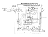
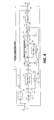
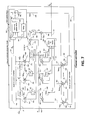
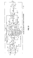
- FIG. 1 shows a block diagram of one embodiments of blind mode adaptive equalizer system.
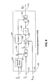
- FIG. 2 shows one embodiment of the digital communication system with blind mode adaptive equalizer system.
- FIG. 3A shows a block diagram one embodiment of differential encoder.
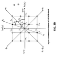
- FIG. 3B shows the signal constellation diagram of 16QAM signal.
- FIG. 4 shows a block diagram of one embodiment of differential decoder.
- FIG. 5 shows a block diagram of one embodiment of channel gain normalizer.
- FIG. 6 shows a block diagram of one embodiment of blind mode adaptive equalizer with hierarchical structure (BMAEHS) with linear equalizer.
- BMAEHS blind mode adaptive equalizer with hierarchical structure
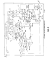
- FIG. 7 shows a block diagram of one embodiment of channel estimator.
- FIG. 8 shows a block diagram of one embodiment of correction signal generator for linear equalizer.
- FIG. 9 shows one embodiment of the FFT Implementation of the correction signal generator.
- FIG. 10 shows a block diagram of one embodiment of blind mode adaptive equalizer with hierarchical structure with decision feedback equalizer.
- FIG. 11 shows one embodiment of the correction signal generator for decision feedback equalizer.
- FIG. 12 shows a block diagram of one embodiment of blind mode adaptive equalizer with hierarchical structure and with orthogonalizer.
- FIG. 13 shows one embodiment of correction signal vector normalizer.
- FIG. 14 shows a block diagram of one embodiment of the cascaded equalizer.
- FIG. 15 shows a block diagram of one embodiment of block diagram of the adaptive digital beam former system
- FIG. 16 shows one embodiment of an example computer device.
- FIG. 1 shows a block diagram for one of the various embodiments of the invention.
- K 1 denoting some reference positive integer.
- a I,k and a Q,k denoting the real and imaginary components of a k taking possible values +A 0 and ⁇ A 0 for some constant A 0 >0.
- each of a I,k and a Q,k may take possible values from the set of N values given by ⁇ 1, ⁇ 3, . . . , ⁇ (N ⁇ 1) ⁇ A 0 .
- T denotes matrix transpose.
- the output of the discrete-time channel is given by the convolution of the input data symbol sequence a k with the channel impulse response h cT given in (2a).
- the output 3 of the discrete-time channel is modified in the adder 5 by the channel noise 4 n k+ K 1 c of variance 2 ⁇ n 2 generating the signal z k+ K 1 c .
- the noisy channel output signal 6 z k+ K 1 c given by (2b) is input to the blind mode adaptive equalizer system 80 .
- H denotes the matrix conjugate transpose operation and * denotes the complex conjugate operation.
- the noisy channel output signal 6 z k+ K 1 c is input to the channel gain normalizer block 7 .
- the channel gain normalizer estimates the average signal power at the output of the discrete-time channel and normalizes the noisy channel output signal 6 such that the signal power at the output of the channel gain normalize 7 remains equal to some desired value even in the presence of the time-varying impulse response of the discrete-time channel as is the case with the fading dispersive channels in digital communication systems.
- the output 8 of the channel gain normalize 7 is given by
- Equation (3) may alternatively be written in the form of (4).
- x k 0 is the channel state vector given by (2a).
- BMAEHS blind mode adaptive equalizer with hierarchical structure
- the equalizer filter 9 may be a linear or a decision feedback filter, or a more general nonlinear equalizer filter characterized by a time varying parameter vector 15 ⁇ k .
- the detected symbol 12 a k+M 1 d is fed back to the equalizer filter 9 via the delay block 13 that introduces a delay of one sample as shown in FIG. 1 .
- the output 12 b of the delay 13 is inputted to the equalizer filter 9 .
- the equalizer state vector 14 ⁇ k is also comprised of the various delayed versions of detected symbol 12 a k+M 1 d .
- the gain normalizer output also referred to as the normalized channel output 8 z k+K 1 , is input to the delay 31 that introduces a delay of K 1 samples in the input 38 and provides the delayed version 32 z k to the model error estimator and the correction signal generator (MEECGS) block 17 of the level 2 adaptive system 50 .
- the detected data symbol 12 at the output of the decision device 11 , and the equalizer parameter vector 15 ⁇ k are input to (MEECGS) block 17 .
- the MEECGS block 17 estimates the channel impulse response vector h T from the detected symbol 12 a k+M 1 d and the delayed normalized channel output 32 z k , determines any modeling error made by the level 1 adaptive system 40 and generates the correction signal 18 ⁇ k c 2 to mitigate such a modeling error.
- the estimate of the data symbols 12 a k+M 1 during the initial period of convergence of the BMAEHS of length N d has relatively high probability of error.
- the initial period of convergence N d is the time taken by the BMAEHS 60 to achieve some relatively small mean squared equalizer error measured after the first N 1 +1 samples at the output 8 of the channel gain normalize 7 are inputted to the BMAEHS 60 and may be selected to be about 100-200 samples.
- the data symbols during the initial convergence period are recovered by the initial data recovery block 75 of FIG. 1 .
- the output 8 of the channel gain normalize 7 z k+K 1 is inputted to the quantizer block 19 .
- the quantizer 19 may quantize the input samples to (n q +1) bits with n q denoting the number of magnitude bits at the quantizer output, so as to minimize the memory requirements for storing the initial segment of the channel gain normalizer output.
- the number of quantizer bits may be selected on the basis of the signal to noise power ratio expected at the noisy channel output signal 6 so that the variance of the quantization noise is relatively small compared to the variance of the channel noise.
- the signal to quantization noise power ratio is given approximately by 6(n q +1) dB and a value of n q equal to 3 may be adequate.
- the quantizer may be eliminated and the channel gain normalizer output 8 z k+K 1 may be directly inputted to the delay 21 .
- the output of the quantizer 20 z k+K 1 q is inputted to the delay 21 that introduces a delay of N d samples.
- the output of the delay 21 is inputted to the fixed equalizer 24 .
- the fixed equalizer is comprised of the cascade of the equalizer filter and the decision device blocks similar to the equalizer filter 9 and the decision device 11 blocks respectively of the BMAEHS 60 .
- the switch S 1 is closed and the fixed equalizer parameter vector 33 ⁇ k f is set equal to the equalizer parameter vector 15 ⁇ k at the time of closing the switch and remains fixed for k+K 1 >N I .
- the detected symbol 12 a k+M 1 d is input to the delay 29 that introduces a delay of N d samples.
- the output 27 of the delay 29 equal to a k+M 1 ⁇ N d d is connected to the position 3 of the switch S 2 26 .
- the position 1 of the switch S 2 26 is connected to the ground.
- the switch S 2 26 remains in position 1 and the output of the switch S 2 26 is equal to 0 during this period.
- the switch S 2 26 is connected to position 2 and the final detected data 30 a k+M 1 ⁇ N d d f is taken from the output of the fixed equalizer 24 .
- the output of the switch S 2 26 is taken from the output of the BMAEHS 60 .
- the output of the switch S 2 26 constitutes the final detected data symbol 30 a k+M 1 ⁇ N d d f .
- the recovery of the initial data segment may not be required and the initial data segment recovery block of FIG. 1 may not be present.
- the final detected symbol output is taken directly from the output of the BMAEHS.
- the detected symbol 12 a k+M 1 d may be inputted to the channel gain normalizer block 7 .
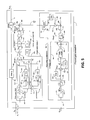
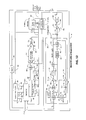
- FIG. 2 shows the block diagram of a digital communication system 101 embodying the blind mode adaptive equalizer system 80 of FIG. 1 .
- the information data sequence 110 d i possibly taking binary values 0 and 1 is input to the error correction code encoder and the interleaver block 111 .
- the error correction coding and the interleaving operations on the information data are performed to protect the information data 110 d i from the possible errors caused due to various channel noise, disturbances, and interference.
- the coded data bits sequence c i at the output 112 of the error correction code encoder and the interleaver block 111 may also be taking binary values.
- the sequence of baseband symbols 114 b k is input to the differential encoder block 115 .
- the differential encoder block 115 transforms the sequence of baseband symbols 114 b k into another complex valued sequence of data symbols 116 a k wherein the signal constellation of a k is same as that of the sequence b k .
- the signal constellation of a k is same as that of the sequence b k .
- both a I,k and a Q,k may take possible values A 0 and ⁇ A 0 .
- the differential encoder 115 protects the information data 110 against possible phase ambiguity introduced at the receiver.
- the phase ambiguity may arise, for example, in the generation of the reference carrier signal, not shown, using nonlinear processing of the received signal as by the use of a fourth power nonlinearity in the case of QPSK modulation.
- the band limiting filter 117 may be a square root raised cosine filter used to minimize the bandwidth required for the transmission of the modulated RF signal.
- R s is the symbol rate of the data symbols a k and r with 0 ⁇ r ⁇ 1 denotes the filter roll off factor as compared to a zero crossing bandwidth of the input data symbol sequence a k equal to R s .
- the band limited symbol sequence 118 u k is inputted to the complex baseband to RF converter block 119 that shifts the center frequency of the spectrum of the signal 118 u k to the RF or possibly an intermediate (IF) frequency.
- the complex baseband to RF converter block 119 may in general have several stages including the conversion to the RF or some intermediate frequency (IF), and digital to analog conversion.
- the RF signal 120 u RF (t) at the output of the complex baseband to RF converter block 119 is inputted to the RF back end block 121 that is comprised of the RF band pass filter, the power amplifier, and possibly conversion from IF to RF frequency.
- the amplified signal 122 u T (t) is connected to the transmit antenna 123 for transmission of the RF signal into the wireless channel that may exhibit multipath propagation and fading resulting in the introduction of the inter symbol interference (ISI) in the transmitted signal.
- ISI inter symbol interference
- the RF signal at the output of the wireless channel is received by the receive antenna 124 providing the received RF signal 125 ⁇ R (t) to the input of the RF front end block 126 of receiver 100 .
- the RF front end block may be comprised of a low noise amplifier (LNA), RF band pass filter, other amplifier stages, and possibly conversion from RF to IF and provides the amplified RF signal 127 ⁇ RF (t) at the output of the RF front end block.
- LNA low noise amplifier
- the receive antenna 124 and the RF front end block 126 may introduce additive noise including the thermal noise into the signal RF signal in the process of receiving and amplifying the RF signal at the output of the wireless channel.
- the amplified RF signal 127 is inputted to the RF to complex baseband converter block 128 that down converts the RF signal to the complex baseband signal 129 .
- the RF to complex baseband converter block 128 may be comprised of a RF to IF down converter, the IF to complex baseband converter and an analog to digital converter.
- the complex baseband signal 129 ⁇ k at the output of the RF to complex baseband converter block 128 is inputted to band limiting matched filter block 130 that may be comprised of a band limiting filter that is matched to the band limiting filter used at the transmitter and a down sampler.
- the band limiting filter 130 at the receiver is also the same square root raised cosine filter 117 at the transmitter.
- the design of the band limiting matched filter block 130 and various other preceding blocks both in the transmitter and receiver are well known to those skilled in the art of the field of this invention.
- the output 6 z k+ K 1 c with K 1 denoting some reference positive integer, of the band limiting matched filter block 130 is inputted to the blind mode adaptive equalizer system 80 .
- the blind mode adaptive equalizer system is comprised of the channel gain normalizer 7 , the blind mode adaptive equalizer with hierarchical structure (BMAEHS) 60 and the initial data segment recovery circuit 75 .
- the details of the blind mode adaptive equalizer system 80 are shown in FIG. 1 .
- the cascade of the various blocks comprised of the band limiting filter 117 , complex baseband to RF converter 119 , the RF back end 121 and the transmit antenna 123 , at the transmitter, wireless communication channel, and the receive antenna 124 , the RF front end 126 , RF to complex baseband converter 128 and the band limiting matched filter 130 at the receiver may be modeled by the cascade comprised of an equivalent discrete time channel 2 with input symbols a k+ K 1 with K 1 denoting some positive reference integer wherein a channel noise 4 n k+ K 1 is added to the output of the channel 2 as shown in FIG. 1 .
- the equivalent discrete time channel may have some unknown impulse response h c that models the combined response of all the blocks in the said cascade.
- the channel gain normalizer 7 estimates the average signal power at the output of the equivalent discrete-time channel and normalizes the noisy channel output such that the signal power at the output of the channel gain normalizer remains equal to some desired value even in the presence of the time-varying impulse response of the discrete-time channel as is the case with the fading dispersive channels in the digital communication system of the FIG. 2 .
- the BMAEHS 60 mitigates the impact of the inter symbol interference that may be caused by the multipath propagation in the wireless channel without requiring any knowledge of the channel impulse response or the need of any training sequence.
- the detected symbols during the initial convergence time of the BMAEHS may have relatively large distortion.
- the differential decoder block 131 performs an inverse operation to that performed in the differential encoder block 115 at the transmitter generating the sequence of the detected baseband symbols 132 b k+M 1 ⁇ N d d at the output.
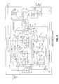
- FIG. 3A shows the block diagram of the differential encoder 115 unit of FIG. 2 for the modulated signal such as QAM, MPSK or ASK.
- the baseband symbol b k is inputted to the tan 2 ⁇ 1 ( ) block 203 that provides the four quadrant phase ⁇ b,k of the input b k at the output with taking values between 0 and 2 ⁇ .
- the phase ⁇ b,k is inputted to the phase threshold device 205 that provides the output 206 ⁇ r,k according to the decision function D p ( ) given by equation (6).
- S denotes the order of rotational symmetry of the signal constellation diagram of the baseband signal b k equal to the number of distinct phase rotations of the signal constellation diagram that leave the signal constellation unchanged and is equal to the number of phase ambiguities that may be introduced by the blind mode equalizer.
- FIG. 3B shows the signal constellation diagram of the 16 QAM signal that has order of rotational symmetry S equal to 4 with the possible phase ambiguities equal to 0, ⁇ /2, ⁇ , 3 ⁇ /2 as the rotation of the signal constellation diagram by any of the four values 0, ⁇ /2, ⁇ , 3 ⁇ /2 leaves the signal constellation unchanged.
- the range of the phase given by ⁇ t i ⁇ b,k ⁇ t i+1 defines the i th sector of the signal constellation diagram equal to the i th quadrant of the signal constellation diagram in FIG.
- the output of the phase threshold device 205 is equal to the reference phase ⁇ i for the i th sector if ⁇ b lies in the i th sector or quadrant.
- the output of the phase threshold device 205 base phase 206 ⁇ r,k is equal to one of the S possible values ⁇ 0 , . . . , ⁇ S-1
- the minimum reference phase ⁇ 0 is subtracted from the base phase 206 ⁇ r,k by the adder 209 .
- the output 215 ⁇ i,k of the adder 209 is inputted to the phase accumulator 210 comprised of the adder 216 , mod 2 ⁇ block 218 and delay 222 , provides the output 221 ⁇ c,k according to equation (2b).
- the mod 2 ⁇ operation is defined as
- ⁇ x ⁇ denotes the highest integer that is smaller than x for any real x.
- mod 2 ⁇ block 218 in FIG. 3A is to avoid possible numerical build up of the accumulator output phase 221 by keeping the accumulator output 221 within the range 0 to 2 ⁇ for all values of time k.
- the phase accumulator output 221 is inputted to the adder 224 that adds the phase ⁇ 0 providing the output 226 ⁇ p,k to the adder 227 .
- ⁇ 0 ⁇ /4 and ⁇ i,k takes possible values 0, ⁇ /2, ⁇ , 3 ⁇ /2.
- the output 221 ⁇ c,k of the phase accumulator can also have 0, ⁇ /2, ⁇ , 3 ⁇ /2 as the only possible values.
- the output 226 ⁇ p,k of the differential phase encoder 220 has ⁇ /4, 3 ⁇ /4, 5 ⁇ /4, 7 ⁇ /4 as the only possible values.
- the signal 206 ⁇ r,k is subtracted from the signal 204 ⁇ b,k by the adder 207 providing the output 208 ⁇ d,k to the adder 227 that adds 208 ⁇ d,k to the differential phase encoder output 226 ⁇ p,k providing the phase of the encoded signal 228 ⁇ a,k at the output.
- the baseband symbol b k is inputted to the absolute value block 201 that provides the absolute value 202
- the output 116 a k
- exp(j ⁇ a,k ); j ⁇ square root over ( ⁇ 1) ⁇ of the multiplier 232 is the differentially encoded data symbol a k .
- the process of differential encoding leaves the magnitude of the symbol unchanged with
- FIG. 3B illustrates the encoding for the 16QAM signal.
- the subscript k on various symbols has been dropped for clarity.
- ⁇ c,k ⁇ 1 is equal to ⁇ resulting in phase ⁇ c,k equal to ⁇ .
- the phase threshold device 205 D p ( ) is bypassed with the output 206 ⁇ r,k equal to the phase 204 ⁇ b,k and with the phase 208 ⁇ d,k equal to 0.
- FIG. 4 shows the block diagram of the differential decoder 131 unit of FIG. 2 .
- the detected data symbol a k d is inputted to the tan 2 ⁇ 1 ( ) lock 242 providing the phase ⁇ a,k of a k d , at the output 243 .
- the phase 243 ⁇ a,k is inputted to the phase threshold device 245 that provides the output phase 244 ⁇ o,k computed according to the decision function D p ( ) given by equation (6).
- the output of the phase threshold device 245 is inputted to the differential phase decoder 270 providing the phase ⁇ r,k at the output 259 . Referring to FIG.
- the detected data symbol 30 a k d is inputted to the absolute value block 240 providing the absolute value 241
- exp(j ⁇ b,k ); j ⁇ square root over ( ⁇ 1) ⁇ at the multiplier 262 output.
- the detected baseband symbols 132 are input to the complex baseband to data bit mapper 133 that maps the complex baseband symbols 132 into groups of m binary bits each based on the mapping used in the complex baseband modulator block 113 at the transmitter.
- the sequence of the detected coded data bits 134 ⁇ i at the output of the complex baseband to data bit mapper block 133 is inputted to the error correction code decoder and deinterleaver block 135 that performs inverse operations to those performed in the error correction code encoder and interleaver block 111 at the transmitter and provides the detected information data sequence 136 ⁇ circumflex over (d) ⁇ i at the output.
- the band limiting filter may intentionally introduce some ISI caused by selecting the symbol rate to be higher than the Nyquist rate so as to increase the channel capacity.
- the blind mode adaptive equalizer system 80 of FIGS. 1 , 2 will also mitigate the ISI arising both due to the intentionally introduced ISI and that arising from the wireless channel.
- FIG. 5 shows the block diagram of the channel gain normalizer 7 .
- the noisy channel output 6 is input to the norm square block 310 that provides ⁇ k 0
- the initial value of the accumulator output ⁇ ⁇ 1 a is set equal to 0, and ⁇ P , 0 ⁇ p ⁇ 1, is a constant that determines the effective period of accumulation in the limit as k 0 ⁇ and is approximately equal to 1/(1 ⁇ p ), for example, ⁇ P may be selected equal to 0.998.
- the average power estimate 342 P T,k 0 is input to the adder 343 that subtracts the estimate of the noise variance 344 ⁇ circumflex over ( ⁇ ) ⁇ n 2 from 342 P T,k 0 resulting in the estimate 345 P c,k 0 of the signal power at the discrete-time channel 2 output.
- the noise variance estimate 344 may be some a-priori estimate of the channel noise variance or may be set equal to 0.
- the desired signal power may be normalized by an arbitrary positive constant, for example by A 0 2 with A 0 simultaneously normalizing the threshold levels in (23)-(24) of the decision device 11 and the expected value E[
- the channel gain G k 0 is made available to the multiplier 353 .
- the initial convergence rate of the BMAEHS 60 may be increased by adjusting the channel gain G k by a factor ⁇ k that is derived on the basis of the statistics of the detected symbol a k d at the output 12 of the BMAEHS.
- ]; a k a I,k +ja Q,k , respectively with convergence, where E denotes the expected value operation.
- the detected symbol a k+M 1 d is inputted to the absolute value
- c
- the output 374 ⁇ k 374 of the switch S is inputted to the averaging block 395 that averages the input ⁇ k over consecutive periods of n s samples.
- the averaging period n s may be selected to be equal to 10.
- the averaging block is comprised of the delay 376 , adder 377 , delay 379 , down sampler 385 , and multiplier 382 . Referring to FIG.
- the output of switch S is inputted to the adder 377 and to the delay 376 that provides the delayed version ⁇ k ⁇ n s to the adder 377 .
- the output of the adder 377 ⁇ k s is input to the delay 379 providing output 380 ⁇ k ⁇ 1 s to the input of the adder 377 .
- the output of the adder 377 may be written as
- the output ⁇ k s of the adder 377 is inputted to the down sampler 385 that samples the input 378 at intervals of n s samples with the output 381 ⁇
- the multiplier 382 normalizes the input ⁇
- m ⁇
- c ] ⁇ ⁇ 1 may measure the deviation of the magnitude of the real and imaginary components of the BMAEHS 60 output from the expected values E[
- m is inputted to the multiplier 388 that multiplies e
- the output of the adder ⁇ 1 is inputted to the delay 391 .
- the output 394 ⁇ 1-1 of the delay 391 is inputted to the adder 390 that provides the output 392 ⁇ 1 according to ⁇
- ⁇
- the output 392 ⁇ 1 of the adder 390 is inputted to the up sampler block 393 that increases the sampling rate by a factor n s using sample hold.
- the output 396 ⁇ k 0 of the sampler block 393 is inputted to the multiplier 353 that adjusts the channel gain estimate G k 0 by a k 0 providing the output 354 G k 0 m to the divider 365 .
- the noisy channel output 6 z k 0 c is input to delay block 361 that introduces a delay of N p samples that is the number of samples required to provide a good initial estimate of G k 0 m and may be selected equal to 50.
- the parameter ⁇ k matches the amplitude of the real and imaginary components of the normalized channel output to the threshold levels of the slicers in the decision device, thereby also making the probability distribution of the detected data symbols a k d equal to the probability distribution of the data symbols a k .
- This can also be achieved in an alternative embodiment of the invention by making the dominant center element h 0 of the normalized channel impulse response h equal to 1.
- the parameter ⁇ k may be estimated in terms of the channel dispersion defined as
- ⁇ k may be estimated to be 1.
- the parameter ⁇ k may also be set to 1.
- the parameter may be estimated adaptively so as to make the dominant element of the normalized channel impulse response approach 1.
- ⁇ a is some small positive constant and ⁇ o may be set to 1.
- the equalizer filter in the equalizer filter block may be a linear, a decision feedback or a more general nonlinear equalizer filter based on the equalizer parameter vector ⁇ k that provides the linear estimate of the data symbol on the basis of the normalized channel output z k+K 1 .
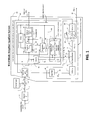
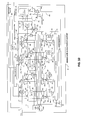
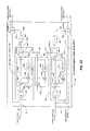
- FIG. 6 shows the block diagram of the BMAEHS 60 of FIG. 1 in one of the various embodiments of the invention.
- the equalizer filter 9 is a linear equalizer filter.
- the output of the channel gain normalizer block 8 also referred to as the normalized channel output z k+K 1 is input to a cascade of 2N 1 delay elements 401 providing the delayed versions 402 of z k+K 1 denoted by z k+K 1 ⁇ 1 , . . . , z k ⁇ N 1 +M 1 at their respective outputs.
- the normalized channel output and its various delayed versions 402 are input to the N wm multipliers 403 wm 1 , . . .
- the N wm multipliers 403 are inputted by the conjugates 406 of the components 405 of the equalizer parameter vector ⁇ ⁇ N 1 ,k , . . . , ⁇ 0,k , . . . , ⁇ N 1 ,k .
- the wm multipliers 403 wm 1 , . . . , wm N multiply the normalized channel output and its delayed versions 402 by the respective conjugates 406 of the components of the equalizer parameter vector ⁇ k generating the respective products 407 at the outputs of the wm multipliers 403 .
- the outputs of the wm multipliers 407 are inputted to the summer 408 providing a linear estimate 10 â k+M 1 of the data symbol at the output of the summer 408 .
- the linear estimate 10 â k+M 1 is input to the decision device 11 that generates the detected symbol 12 a k+M 1 d , at the output of the decision device 11 based on the decision function ⁇ ( ).
- the decision function may be given by (20).
- D ( â I,k +jâ Q,k ) D I ( â I,k )+ jD Q ( â Q,k ) (20)
- the functions ⁇ I ( ) and ⁇ Q ( ) may be the slicer functions.
- the two slicer functions ⁇ I (x) and ⁇ Q (x) with x real are identical and are given by (21).
- ) iA 0 ;V t i ⁇ 1 ⁇
- ⁇ V t i ;i 1,2 , . . . ,N/ 2 (23)
- the decision function described by (20) (24), for example, applies to the case where a k is obtained as a result of MQAM modulation in the digital communication system of FIG. 2 , with the number of points in the signal constellation M N 2 .
- other appropriate decision functions may be employed.
- the decision device may comprise of a normalizer that normalizes the complex data symbol by its magnitude with the normalized data symbol operated by the decision function in (20)-(24).
- the error signal 410 e k is input to the conjugate block 411 .
- the output of the conjugate block 412 e k * is multiplied by a positive scalar 413 ⁇ d in the multiplier 414 .
- the output of the multiplier 414 is input to the N weight correction multipliers 415 wcm 1 , . . .
- wcm N wherein it multiplies the normalized channel output z k+K 1 and its various delayed versions 401 z k+K 1 ⁇ 1 , . . . , z k ⁇ N 1 +M 1 generating the N components 419 of ⁇ d w k c 1 with the first correction vector w k c 1 given by (26).
- w k c 1 ⁇ k e k *;
- the second parameter correction vector 452 w k c 2 generated by the MEECGS for LEQ block 50 is multiplied by a positive scalar 453 ⁇ by the multiplier 454 .
- the multiplier output 455 is connected to the vector to scalar converter 460 that provides the N components 461 of the vector ⁇ w k c 2 given ⁇ w ⁇ N 1 ,k c 2 , . . . , ⁇ w o,k c 2 , . . . , ⁇ w N 1 ,k c 2 at the output of the vector to scalar converter 460 .
- the equalizer parameter components ⁇ ⁇ N 1 ,k , . . . , ⁇ 0,k , ⁇ N 1 ,k at the outputs of the N delay elements 421 are input to the wca adders 420 .
- the wca adders 420 add the equalizer parameter components 422 ⁇ ⁇ N 1 ,k , . . . , ⁇ 0,k , . . .
- the output 422 of the N wca adders 420 are connected to the N delay elements 421 .
- the outputs 405 of the N delay elements 421 are equal to the equalizer parameter vector components 405 ⁇ ⁇ N 1 ,k , . . . , ⁇ 0,k , . . . , ⁇ N 1 ,k that are inputted to the N conjugate blocks 404 .
- the detected symbol 12 a k+M 1 d is inputted to the channel estimator 440 .
- the normalized channel output 8 z k+K 1 is input to the delay block 435 that introduces a delay of K 1 samples providing the delayed version 436 z k to the input of the channel estimator 440 .
- the channel estimator 440 provides the estimate of the channel impulse response vector 442 ⁇ k at the output of the channel estimator.
- ⁇ N 1 ,k are input to the scalar to vector converter 430 that provides the equalizer vector 432 ⁇ k to the correction signal generator for LEQ 450 .
- the estimate of the channel impulse response vector 442 ⁇ k is input to the correction signal generator 450 that provides the second correction signal vector 452 w k c 2 to the multiplier 454 .
- the correction signal generator 450 convolves the estimate of the channel impulse response vector 442 ⁇ k T ; with the equalizer parameter vector 432 ⁇ k T to obtain the convolved vector ⁇ k T .
- the difference between the vector ⁇ k T obtained by convolving the estimate of the channel impulse response vector ⁇ k T with the equalizer parameter vector ⁇ k T , and the ideal impulse response vector
- a large deviation of the convolved response ⁇ k T from the ideal impulse response implies a relatively large modeling error.
- the correction signal generator block generates a correction signal 452 ⁇ k c 2 on the basis of the modeling error vector [ ⁇ K 1 ,K 1 ⁇ ⁇ k ] and inputs the correction signal 452 w k c 2 to the adaptation block 16 for adjusting the equalizer parameter vector ⁇ k+1 at time k+1.
- the first correction signal vector w k c 1 may be based on the minimization of the stochastic function
- the update algorithm in (27a) reduces to the decision directed version of the LMS algorithm.
- the first correction signal vector may be derived on the basis of the optimization of the objective function in (28)
- the algorithm in (30) may result in a faster convergence compared to that in (27).
- the vector ⁇ k q is obtained by replacing both the real and imaginary components of the various components of the vector ⁇ k with the 1 bit quantized versions.
- sgn(x) for x real is the signum function defined in (22), and Re(z) and Im(z) denote the real and imaginary components of z for any complex variable z.
- h i , ⁇ M 1 , . . . , 0, . . . , M 1 are the components of the channel impulse response vector h related to the vector h c via the channel gain G k m shown in FIG. 5 .
- an exponentially data weighted least squares algorithm for the estimate of the channel impulse response vector ⁇ k may be obtained by minimizing the optimization index l 1,k with respect to h
- P ⁇ 1 ⁇ 1 ⁇ I for some small positive scalars ⁇ and with I denoting the identity matrix.
- the RLS algorithm (36) is used for the estimation
- an exponentially data weighted Kalman filter algorithm may be used.
- the Kalman filter minimizes the conditional error variance in the estimate of the channel impulse response given by E[ ⁇ h ⁇ ⁇ ⁇ 2 /z 0 , z 1 , . . . , z k ], where E denotes the expected value operator.
- one of the class of quantized state algorithms may be used for the estimation of h .
- the quantized state algorithms possess advantages in terms of the computational requirements.
- x q is obtained from x by replacing both the real and imaginary components of each component of x by their respective signs taking values +1 or ⁇ 1.
- Multiplication of x q by the matrix P q in (38b) requires only additions instead of both additions and multiplications, thus significantly reducing the computational requirements.
- the channel input a k appearing in the state vector x k in (34)-(38) is replaced by the detected symbol a k d .
- the modified RLS algorithm (40a)-(40b) is used for the estimation of the channel impulse response h .
- the Kalman filter algorithms in (37) or the quantized state algorithm in (38) with the state vector x k replaced with the estimate ⁇ circumflex over (x) ⁇ k may be used for the estimation of the channel impulse response h .
- FIG. 7 shows the block diagram of the channel estimator block 440 of FIG. 6 .
- the detected symbol 12 a k+M 1 d from the output of the decision device 11 is input to a cascade of 2M 1 delay elements 510 generating the 2M 1 delayed versions 512 a k+M 1 ⁇ 1 d , . . . , a k ⁇ M 1 d at the outputs of the delay elements.
- the M hm multipliers 514 are inputted with the conjugates 518 of the M components 516 ⁇ ⁇ M 1 ,k ⁇ 1 , . . . , ⁇ 0,k ⁇ 1 , . . . , ⁇ M 1 ,k ⁇ 1 of the channel impulse response vector ⁇ k ⁇ 1 provided by the conjugate blocks 517 .
- the M hm multipliers 514 multiply the detected symbols a k+M 1 d , . . . , a k ⁇ M 1 d by the respective components ⁇ ⁇ M 1 ,k ⁇ 1 , . . . , ⁇ 0,k ⁇ 1 , . . .
- the outputs of the M hm multipliers 514 are inputted to the summer 575 that provides the sum of the inputs representing the predicted value 576 ⁇ circumflex over (z) ⁇ k of the normalized channel output z k at the summer output 576 .
- the error signal 579 e k h is inputted to the conjugate block 580 , the output of 581 of the conjugate block 580 is multiplied by a positive scalar ⁇ h in the multiplier 583 .
- the output 584 of the multiplier 583 is input to the M weight correction multipliers 526 hcm 1 , . . . , hcm N wherein e k h * multiplies the M components K ⁇ M 1 ,k , . . . , K 0,k , . . . , K M 1 ,k of the gain vector 548 K k provided by the vector to scalar converter 560 .
- the outputs of the hcm 1 , . . . , hcm M multipliers 526 are input to the N hca adders 518 hca 1 , . . . , hca M .
- the M hca adders 518 are inputted with the M components ⁇ ⁇ M 1 ,k ⁇ 1 , . . . , ⁇ 0,k ⁇ 1 , . . . , ⁇ M 1 ,k ⁇ 1 of the channel impulse response vector ⁇ k ⁇ 1 at the outputs of the M delay elements 520 and with the outputs 522 of the M hcm multipliers 526 .
- the hca adders 518 add the M channel impulse response vector components ⁇ ⁇ M 1 ,k ⁇ 1 , . . . , ⁇ 0,k ⁇ 1 , . . .
- the channel state vector 530 ⁇ circumflex over (x) ⁇ k is input to the gain update block 550 that provides the gain vector 548 K(k) to the vector to scalar converter 560 .
- the channel state vector 530 ⁇ circumflex over (x) ⁇ k and the matrix 545 P k ⁇ 1 are input to the matrix P k update block 542 that evaluates the updated matrix 543 P k according to equation (36b) and provides the updated matrix 543 P k to the delay 544 .
- the output 545 of the delay 544 equal to P k ⁇ 1 is inputted to the matrix P k update block 542 .
- the gain vector 548 K k is inputted to the vector to scalar converter 560 .
- the elements of the vector k are obtained by the discrete convolution of the sequences ⁇ h ⁇ M 1 . . . , h ⁇ 1 , h 0 , h 1 , . . . , h M 1 ⁇ and ⁇ w ⁇ N 1 , . . . , w ⁇ 1 , w 0 , w 1 , . . . , w N 1 ⁇ .
- the sequences are also represented as vectors h and w respectively with the similar notations for the other sequences.
- H 1 [ h - M 1 0 0 ... 0 h - M 1 + 1 h - M 1 0 ... 0 ... ... ... h M 1 ... h 0 ... h - M 1 ] ( 44 ⁇ a )
- H 2 [ h M 1 ... h 0 ... h - M 1 0 ⁇ ⁇ h M 1 ... h 0 ... h - M 1 + 1 ... ... ... 0 ⁇ ⁇ 0 ... 0 h M 1 ] ( 44 ⁇ b )
- H 3 [ 0 h M 1 ... h 0 ... h - M 1 00 ⁇ ⁇ ... ⁇ 0 ⁇ N - M - 1 0 0 h M 1 ... h 0 ... h - M 1 0 ⁇ ⁇ ... ⁇ 0 ... ... ... 00 ⁇ ⁇ ... ⁇ 0 0 ⁇
- the matrix H in (44d) can be appropriately modified for the case of N 1 ⁇ M 1 .
- the equalizer parameter vector w can be selected so that the impulse response of the composite system g T given by (42) is equal ⁇ K 1 ,K 1 to which is defined for any pair of positive integers K 1 , K 1 ′ as
- ⁇ _ K 1 , K 1 ′ [ 00 ⁇ ⁇ ... ⁇ ⁇ 0 ⁇ K 1 1 00 ⁇ ⁇ ... ⁇ ⁇ 0 ⁇ K 1 ′ ] T ( 45 )
- the equalizer parameter vector w may be selected so as to minimize some measure of the difference between g and the unit vectors ⁇ .
- the L 1 norm is given by
- ⁇ j - K 1 K 1 ⁇ ⁇ ( g j - ⁇ j ) ⁇ with ⁇ j denoting the jth component of the vector ⁇ .
- the L ⁇ norm is given by
- optimization function may be selected as
- ⁇ 1 and ⁇ 2 are some positive constants determining the relative weights assigned to J L 2 and J L 4 respectively. Differentiation of J L 4 with respect to the equalizer parameter w i yields
- n th power of any vector x for any real n is defined as taking the component wise n th power of the elements of the vector x ,
- FIG. 8 shows the block diagram of the correction signal generator 450 of FIG. 6 that generates the second correction signal vector 452 ⁇ k c 2 according to (51).
- the estimate of the channel impulse response vector 442 ⁇ k is input to the correction signal generator 450 .
- the output 638 of the conjugate block 635 is inputted to the matrix multiplier 640 .
- the matrix 622 ⁇ k is input to the transpose block 642 that provides the matrix 644 ⁇ k T at the output.
- the matrix 644 ⁇ k T is inputted to the matrix multiplier 640 that multiplies the matrix 644 ⁇ k T by 638 ( ⁇ k ⁇ ⁇ K 1 ,K 1 )* generating the second correction vector 452 w k c 2 at the matrix multiplier output.
- the vector ⁇ k in (51) and (55) can also be obtained by the convolution of the channel impulse response h with the equalizer parameter vector ⁇ k .
- the product 2 ⁇ 2 ⁇ w ⁇ 2 is the noise variance at the equalizer output and ⁇ 3 determines the relative weighting given to power of the residual inter symbol interference (ISI) I s .
- the ISI power is proportional to the summation in the first term on the right hand side of (61) and is given by
- 2 ⁇ ( ⁇ circumflex over ( g ) ⁇ k ⁇ ⁇ )*; k 0,1, (65b) In (65) the parameter ⁇ 0 with 0 ⁇ 0 ⁇ 1, is determined by the relative weight ⁇ 3 .
- ⁇ k and ⁇ k c are given by (61b).
- the convolution operation in the iterative algorithms (59), (60) and (65) can be performed equivalently in terms of the discrete Fourier transform (DFT) or the fast Fourier transform (FFT) operations.
- DFT discrete Fourier transform
- FFT fast Fourier transform
- the FFT operation results in a circular convolution, hence for proper convolution operation the individual vectors to be convolved are zero padded with an appropriate number of zeros.
- the FFT of h I can be related to the FFT of h if a zero is appended at the beginning of the vector h . Therefore, a vector h e of length (N+M+2) is defined by
- h _ e [ 0 ⁇ h - M 1 ⁇ ⁇ ... ⁇ ⁇ h - 1 ⁇ h 0 ⁇ h 1 ⁇ ⁇ ... ⁇ ⁇ h M 1 ⁇ 00 ⁇ ⁇ ... ⁇ ⁇ 0 ⁇ N + 1 ⁇ ] T ( 67 )
- a vector ⁇ k e of length (N+M+2) is defined as
- w _ ⁇ k e [ w ⁇ - N 1 ⁇ ⁇ ... ⁇ ⁇ w ⁇ - 1 ⁇ w ⁇ 0 ⁇ w ⁇ 1 ⁇ ⁇ ... ⁇ ⁇ w ⁇ N 1 ⁇ 00 ⁇ ⁇ ... ⁇ ⁇ 0 ⁇ M + 2 ] T ( 68 )
- the suffix k denoting the time index has been dropped from the elements of the vector ⁇ k e .
- Tr 1 comprised of deleting (M ⁇ 1) elements from each side of the vector in its argument on the left hand side of (75) is equivalent to deleting the last (M+2) elements from the vector on the right hand side of (74).
- Tr 2 [ 00 ⁇ ⁇ ... ⁇ ⁇ 0 ⁇ N 1 - M 1 ⁇ h M 1 ⁇ ⁇ ... ⁇ ⁇ h 1 ⁇ h 0 ⁇ h - 1 ⁇ ⁇ ... ⁇ ⁇ h - M 1 ⁇ 00 ⁇ ⁇ ... ⁇ ⁇ 0 ⁇ N 1 - M 1 ] T ( 77 )
- Tr 2 the truncation operation Tr 2 is comprised of discarding the last (M+2) elements from the vector in its argument
- w _ ⁇ k + 1 w _ ⁇ k - ⁇ ⁇ Tr 2 ⁇ ⁇ F - 1 ⁇ [ ( h _ eF ) * ⁇ • ⁇ [ g _ ⁇ k eF - ⁇ _ F + ⁇ ⁇ ⁇ g _ ⁇ k cF ] ] ⁇ * - ⁇ 0 ⁇ w _ ⁇ k * ( 78 ⁇ a )
- ⁇ k eF is given by (71)
- ⁇ F is the Fourier transform of ⁇ K 1 +1 ,K 1 +3 given by
- ⁇ _ K 1 + 1 , K 1 + 3 [ 00 ⁇ ⁇ ... ⁇ ⁇ 0 ⁇ K 1 + 1 1 00 ⁇ ⁇ ... ⁇ ⁇ 0 ⁇ K 1 + 3 ] T ( 78 ⁇ b ) and is equal to the (K 1 +2) th row of the matrix ⁇ K defined by (70b) with N replaced by (K+3).
- ⁇ k cF denotes the FFT of [0 ⁇ k cT 00] H .
- the second correction signal vector w k c 2 may be given by
- Tr 2 Tr 2 ⁇ ⁇ F - 1 ⁇ [ w _ ⁇ eF ⁇ • ⁇ ⁇ h _ ⁇ eF ⁇ 2 ] ⁇ * - h _ ⁇ k Ie + ( ⁇ 0 / ⁇ ) ⁇ w _ ⁇ k ⁇ * ( 79 )
- ⁇ eF is obtained from (69) after replacing h e by ⁇ k e
- Tr 2 is comprised of discarding the last (M+2) elements from the vector in its argument.
- FIG. 9 shows the FFT implementation of the correction signal generator 450 B of FIG. 6 .
- the equalizer parameter vector 432 ⁇ k is input to the vector to scalar converter 710 that provides the N components 712 ⁇ ⁇ N 1 ,k , . . . , ⁇ 0,k , . . . , ⁇ N 1 ,k of the vector ⁇ k at the output.
- the N components 712 ⁇ ⁇ N 1 ,k , . . . , ⁇ 0,k , . . . , ⁇ N 1 ,k along with (M+2) zeros are input to the (K+3) point FFT1 block 720 .
- the FFT1 block 720 evaluates the (K+3) point FFT transform of the inputs 712 , 714 and provides the (K+3) outputs 735 ⁇ 0,k eF , . . . , ⁇ k+2,k eF to the multipliers 736 ftm 1 , . . . , ftm K+3 .
- the estimate of the channel impulse response vector 442 ⁇ k is input to the vector to scalar converter 724 that provides the M outputs 726 to the inputs of the FFT2 block 730 .
- the other (N+2) inputs 727 , 728 of the FFT2 block 730 are set equal to 0.
- the (K+3) outputs 731 of the FFT2 block 730 ⁇ 0,k eF , . . . , ⁇ K+2 eF are input to the (K+3) modulus square blocks 732 msq 1 , . . . , msq K+3 .
- the outputs 733 of the (K+3) modulus square blocks 732 msq 1 , . . . , msq K+3 are connected to the inputs of the respective (K+3) multipliers 736 ftm 1 , . . . ,ftm K+3 .
- the (i+1) th ftm multiplier ftm i multiplies ⁇ i,k eF with
- 2 and provides the output 737 to the (i+1) th input of the (K+3) point IFFT block 740 for i 0, (K+2).
- the IFFT block 740 evaluates the (K+3) point IFFT of the (K+3) inputs 737 .
- the last (M+2) outputs 749 of the IFFT block 740 are discarded.
- the first 742 (N 1 ⁇ M 1 ) and the last 748 (N 1 ⁇ M 1 ) of the remaining N outputs of the IFFT block 740 denoted by ⁇ 0,k pe , . . . , ⁇ n 1 ⁇ M 1 ⁇ 1,k pe , ⁇ N 1 +M 1 +1,k pe , . . . , ⁇ N-1,k pe are inputted to the respective 2(N 1 ⁇ M 1 ) inputs of the scalar to vector converter 760 .
- ⁇ n 1 +M 1 ,k pe are inputted to the inputs of the M fta adders 746 fta 1 , . . . , fta M that subtract the complex conjugate 751 of the 726 ⁇ ⁇ M 1 ,k , . . . , ⁇ 0,k , . . . , ⁇ M 1 ,k respectively provided by the conjugate block 750 from the inputs 744 provided by the IFFT block 740 by the adders 746 .
- ⁇ M 1 ,k of the vector to scalar converter 734 are provided to the conjugate block 750 .
- the outputs of the M fta adders are inputted to the scalar to vector converter 760 that provides the vector 761
- w _ ⁇ k pc * Tr ⁇ ⁇ F - 1 [ w _ ⁇ k eF ⁇ • ⁇ ⁇ h _ ⁇ k ⁇ eF ⁇ 2 ] ⁇ - h _ ⁇ k Ie * to the conjugate block 762 .
- the output 764 ⁇ k pc of the conjugate block 762 is input to the adder 780 that adds ( ⁇ 0 / ⁇ ) ⁇ k * provided by the multiplier 766 to 764 ⁇ k pc with the result of the addition equal to the second correction signal vector 452 w k c 2 .
- the conjugate of the equalizer parameter vector 432 ⁇ k is inputted to the multiplier 765 .
- the second correction signal vector 452 w k c 2 is inputted to the adaptation block 16 of FIG. 6 .
- ⁇ and ⁇ 0 are small positive scalars and determine the relative weights assigned to the noise and ISI as in ((62)-(65).
- the equalizer filter 9 in the BMAEHS 60 of FIG. 1 may be selected as the decision feedback equalizer (DFE) filter.
- DFE decision feedback equalizer
- some of the components of the equalizer state vector ⁇ k are replaced by the detected symbols that are available at the instance of detecting the present symbol a k+M 1 d .
- the matrix H + is obtained by N+M 1 shifted versions of the channel impulse response vector h , appended with appropriate number of 0s on both sides of h , staring with the first row equal to the first row of the matrix H 1 + in (83b).
- N 2 is selected equal to M 1 .
- the second correction signal vector ⁇ k c 2 in (80a) is obtained by minimizing the norm of the vector with ( ⁇ k m ⁇ ⁇ ) with respect to the vectors ⁇ k + , and ⁇ k ⁇ .
- H k c [ H k + ⁇ O ( K 1 + 1 ) ⁇ M 1 I M 1 ] ( 84 ⁇ b )
- O (K 1 +1) ⁇ M 1 is the (K 1 +1) ⁇ M l matrix with all the elements equal to 0 and I M 1 is the (M 1 ⁇ M 1 ) identity matrix.
- the second correction signal vector w k c 2 may be written in the equivalent form in (86).
- w _ k c 2 [ H k + H ... O M 1 ⁇ ( K 1 + 1 ) I M 1 ] ⁇ ( g _ ⁇ k m - ⁇ _ K 1 , N 2 ) * ( 86 ⁇ a )
- g _ ⁇ k m H k + ⁇ w _ ⁇ k + + w _ ⁇ k - e ( 86 ⁇ b )
- g _ ⁇ k m [ ( g _ ⁇ k 1 ⁇ m ) T ⁇ ( g _ ⁇ k 2 ⁇ m ) T ] T ( 86 ⁇ c )
- w _ k c 2 [ H k + T ⁇ ( g _ ⁇ k m - ⁇ _ K 1 , N 2 ) g _ ⁇ k 2 ⁇ m ] * ( 86 ⁇ d )
- ⁇ k 1m and ⁇ k 2m are vectors of dimension (K 1 +1) and N 2 respectively.
- FIG. 10 shows the block diagram of the BMAEHS block 60 of FIG. 1 for one of the embodiments of the invention incorporating the case of the decision feedback equalizer.
- the normalized channel output 8 z k+K 1 is input to a cascade of N 1 delay elements 801 providing the delayed versions 802 of z k+K 1 denoted by z k+K 1 ⁇ 1 , . . . , z k+K 1 ⁇ N 1 at their respective outputs.
- the normalized channel output 8 and its N 1 various delayed versions 802 are input to the (N 1 +1) wm multipliers 803 wm 1 , . . . , wm N 1 +1 .
- the N wm multipliers 803 , 815 are inputted by the conjugates of the components of the equalizer parameter vector ⁇ ⁇ N 1 ,k , . . . , ⁇ 0,k , . . . , ⁇ N 2 ,k . provided by the conjugate blocks 804 , 816 that are inputted with the components 805 of the equalizer parameter vector ⁇ k .
- the (N 1 +1) wm multipliers 803 multiply the normalized channel output and its N 1 delayed versions 802 by the conjugates 806 of the first N 1 components of the equalizer parameter vector ⁇ k generating the respective products 807 at the outputs of the wm multipliers 803 .
- the outputs 807 of the (N 1 +1) wm multipliers are input to the summer 808 that provides a linear estimate 809 â k+M 1 of the data symbol at the output of the summer 808 .
- the linear estimate 809 â k+M 1 is input to the decision device 11 that generates the detected symbol 12 a k+M 1 d based on the decision function ⁇ ( ) given by (20)-(25).
- the detected symbol 12 a k+M 1 d is input to the cascade of N 2 delays 814 providing the N 2 delayed versions 812 of a K+m 1 d denoted by a k+m 1 ⁇ 1 , . . . ,a k+M 1 ⁇ N 2 d at their respective outputs.
- the N 2 delayed versions 812 of a k+M 1 d are input to the N 2 wm multipliers 815 wm N 1 +2 , . . . ,wm N and are multiplied by complex conjugates 817 of the last N 2 components 805 of the equalizer parameter vector ⁇ 1,k , . . .
- the outputs 818 of the N 2 wm multipliers 815 are input to the summer 808 that provides the linear estimate 809 â k+M 1 of the data symbol at the output.
- the components 802 , 812 z k+K 1 , . . . , z k+K 1 ⁇ N 1 , d k+M 1 ⁇ 1 d , . . . , a k+M 1 ⁇ N 2 d of the state vector ⁇ k are inputted to the wcm multipliers 820 wcm 1 , . .
- the output 826 of the conjugate block 825 is multiplied by the scalar ⁇ d in the multiplier 827 with the output 826 inputted to the N wcm multipliers 820 wcm 1 , . . . , wcm N .
- the detected symbol 12 a K+M 1 d is inputted to the channel estimator 440 .
- the normalized channel output 8 z k+K 1 is input to the delay block 435 that introduces a delay of K 1 samples providing the delayed version 436 z k to the input of the channel estimator 440 .
- the channel estimator 440 provides the estimate of the channel impulse response vector 442 ⁇ k at the output of the channel estimator.
- ⁇ N 2 ,k are input to the scalar to vector converter 840 that provides the equalizer vector 841 ⁇ k to the correction signal generator for DFE block 850 .
- the estimate of the channel impulse response vector 442 ⁇ k is input to the correction signal generator for DFE block 850 that provides the second correction signal vector 842 w k c 2 to the multiplier 843 .
- the correction signal generator for DFE 850 estimates the impulse response ⁇ k mT of the cascade of the channel and the equalizer. The difference between the vector ⁇ k mT and the ideal impulse response vector
- ⁇ _ K 1 , N 2 ⁇ T [ 00 ⁇ ⁇ ... ⁇ ⁇ 0 ⁇ K 1 ⁇ 1 00 ⁇ ⁇ ... ⁇ ⁇ 0 ⁇ N 2 ] may provide a measure of the modeling error incurred by the equalizer.
- a large deviation of the convolved response ⁇ k mT from the ideal impulse response implies a relatively large modeling error.
- the correction signal generator block 850 generates the second correction signal 842 w k c 2 on the basis of the modeling error vector [ ⁇ K 1 ,N 2 ⁇ ⁇ k ] and is given by (85)-(86).
- the second correction signal 842 w k c 2 is inputted to the adaptation block 16 B for adjusting the equalizer parameter vector ⁇ k+1 at time k+1.
- the decision feedback equalizer parameter algorithm implemented by the adaptation block 16 B of FIG. 10 is described by (80). Referring to FIG. 10 , the second correction signal 842 w k c 2 is multiplied by a positive scalar ⁇ providing the product to the vector to serial converter 845 .
- N wca adders 832 are inputted to the N wca adders 832 .
- the outputs of the N wca adders 832 constituting the components of the updated equalizer parameter vector ⁇ k+1 are inputted to the N delays 834 .
- the outputs of the N delays 834 are inputted to the N conjugate blocks 804 .
- FIG. 11 shows the block diagram of the correction signal generator for the decision feedback equalizer 850 of FIG. 10 .
- the vector 868 ⁇ k + is input to the vector to scalar converter 870 that provides the components 871 , 872 , 875 ⁇ ⁇ K 1 ,k + , . . . , ⁇ 0,k + , . . .
- the first K 1 components 871 ⁇ ⁇ K 1 ,k + , . . . , ⁇ ⁇ 1,k + of the vector ⁇ k + are input to the scalar to vector converter 880 .
- the component 872 ⁇ 0,k + subtracts the constant 1 in the adder 873 with the result of the subtraction 874 ( ⁇ 0,k + ⁇ 1) inputted to the scalar to vector converter 880 as shown in FIG. 11 .
- the vector 841 ⁇ k ⁇ is inputted to the vector to scalar converter 2 that provides the components 877 ⁇ 1,k , . . . , ⁇ N 2 ,k at the output of the vector to scalar converter 895 .
- the components 877 ⁇ 1,k , . . . , ⁇ N 2 ,k and the components 875 ⁇ 1,k + , . . . , ⁇ N 2 ,k + of the vector ⁇ k + are inputted to the adders 876 ga 1 , . . . , ga N2 .
- N 2 provides the sum 879 ( ⁇ i,k + + ⁇ i,k ) at the adder output.
- the outputs 879 of the N 2 ga adders 876 are input to the scalar to vector converter 882 that provides the vector 884 ⁇ k 2m at the output.
- the matrix 861 ⁇ k + , from the matrix ⁇ k + collator block is input to the transpose block 862 that provides the matrix 863 ⁇ k +T to the input of the matrix multiplier 886 .
- the matrix multiplier 886 provides the product 887 ⁇ k +T ( ⁇ k m ⁇ ⁇ k 1 ,N 2 ) at the matrix multiplier 886 output and makes the result available to the vector concatenator 2 .
- the vector ⁇ k 2m is inputted to the vector concatenator 2 that concatenates it with the vector ⁇ k +T ( ⁇ k m ⁇ ⁇ K 1 ,N 2 ) providing the concatenated vector 891 to the conjugate block 892 .
- the output 842 of the conjugate block 892 is equal to the second correction signal w k c 2 according to (86).
- the convergence rate of the equalizer parameter vector update algorithm in (27) to (31) may be significantly increased by the application of the orthogonalization procedure
- the sequence of the correction signal vectors is modified such that in the modified sequence, the correction signal vectors at successive time instances k are nearly orthogonal resulting in increased convergence rate.
- the BMAEHS block of FIG. 1 is modified by an orthogonalizer.
- FIG. 12 shows the block diagram of the BMAEHS block 70 incorporating the correction signal vector orthogonalizer that may replace the BMAEHS block 60 in FIG. 1 .
- the normalized channel output 8 z k+K 1 is input to the equalizer block 9 ( 800 ), the number in the paranthesis refers to the case of the embodiment of the invention with the decision feedback equalizer.
- the linear estimate â k+M 1 at the output of the equalizer filter is input to the decision device 11 that generates the detected symbol 902 a k+M 1 d based on the decision function ⁇ ( ).
- the complex conjugate of the error signal 904 e k made available by the conjugate block 905 and the equalizer state vector 907 ⁇ k provided by the equalizer 9 ( 800 ) are inputted to the matrix multiplier 910 .
- the matrix multiplier 901 generates the first correction signal vector 911 w k c 1 that that is made available to the correction signal vectors normalizer 915 . Referring to FIG.
- the MEECGS block 50 ( 810 ) provides the second correction signal vector 912 w k c 2 to the correction signal vectors normalizer 915 .
- the correction signal vectors normalize 915 normalizes the two correction signal vectors 911 , 912 by the square roots of the mean squared norms of the respective correction signal vectors and inputs the normalized correction signal vectors 916 ⁇ k 1 and 917 ⁇ k 2 to the adder 918 .
- the matrix Q ⁇ 1 may be set equal to ⁇ I N with ⁇ equal to some positive scalar and I N denting the N ⁇ N identity matrix.
- ⁇ J is an exponential data weighting coefficient with 0 ⁇ J ⁇ 1 and determines the rate at which the past values of 920 ⁇ k are discarded in the estimation of the matrix Q k as with the application of the matrix inversion lemma, the matrix Q k ⁇ 1 for relatively large value of k may be interpreted as a positive scalar times an estimate of the covariance of ⁇ k , with Q k ⁇ 1 ⁇ ((1 ⁇ J k )/(1 ⁇ J ))E[ ⁇ k ⁇ k H ] where E denotes the expected value operator.
- the normalized correction signal vector 920 ⁇ k is input to the matrix multiplier 921 wherein 920 ⁇ k is pre multiplied by the matrix 922 Q k ⁇ 1 .
- the matrix 922 Q k ⁇ 1 is made available to the matrix multiplier 921 by the output of the delay 944 .
- the output of the matrix multiplier 921 is input to the matrix multiplier 926 .
- the normalized correction signal vector 920 ⁇ k is input to the conjugate transpose block 924 that provides the row vector 929 ⁇ k H to the input of the matrix multiplier 926 .
- the matrix multiplier 921 output 923 equal to Q k ⁇ 1 ⁇ k is inputted to the matrix multiplier 934 and to the conjugate transpose block 937 .
- the matrix multiplier 926 output 927 equal to ⁇ k H Q k ⁇ 1 ⁇ k is input to the adder 928 that adds the constant ⁇ J to the input 927 .
- the output 931 of the adder 928 equal to ( ⁇ k H Q k ⁇ 1 ⁇ k + ⁇ J ) is input to the inverter 932 that makes the result 933 equal to 1/( ⁇ k H Q k ⁇ 1 ⁇ k + ⁇ J ) available to the input of the matrix multiplier 934 .
- the output 935 of the matrix multiplier 934 and the output of transpose block 937 equal to ⁇ k H Q k ⁇ 1 are inputted to the matrix multiplier 936 that provides the matrix product 939 Q k ⁇ 1 ⁇ k ⁇ k H Q k ⁇ 1 /( ⁇ k H Q k ⁇ 1 ⁇ k + ⁇ J ) at the output of the matrix multiplier 936 .
- the outputs of the delay 944 and that of the matrix multiplier 936 are input to the adder 940 that provides the difference between the two inputs at the output of the adder.
- the output 941 of the adder 940 is normalized by the constant ⁇ J in the multiplier 941 .
- the output 943 of the multiplier 941 constitutes the updated matrix 943 Q k that is input to the delay 944 .
- the output of the delay 944 equal to 922 Q k ⁇ 1 is input to the multiplier 921 .
- the normalized channel output 8 z k+K 1 is input to the delay block 435 that introduces a delay of K 1 samples providing the delayed version 436 z k to the input of the channel estimator 440 .
- the detected symbol 902 a k+M 1 d from the output of the decision device 11 is made available to the channel estimator 440 .
- the channel estimator 440 provides the estimate of the channel impulse response vector 442 ⁇ k at the output of the channel estimator and to the input of the correction signal generator 450 ( 850 ).
- the equalizer filter 9 ( 800 ) in FIG. 12 is the linear equalizer filter and the correction signal generator block is the same as the correction signal generator block for LEQ 450 of FIG.
- the correction signal generator 450 convolves the estimate of the channel impulse response vector 442 ⁇ k T with the equalizer parameter vector 950 ⁇ k T to obtain the convolved vector ⁇ k T .
- the difference between the vector ⁇ k T obtained by convolving the estimate of the channel impulse response vector with the equalizer parameter vector ⁇ k , and the ideal impulse response vector ⁇ K 1 ,K 2 may provide a measure of the modeling error incurred by the equalizer.
- a large deviation of the convolved response ⁇ k T from the ideal impulse response implies a relatively large modeling error.
- the correction signal generator block 450 generates the second correction signal vector 912 w k c 2 on the basis of the modeling error vector [ ⁇ K 1 ,K 2 ⁇ ⁇ k ].
- the second correction signal vector 912 w k c 2 is inputted to the correction signal vectors normalizer block 915 .
- the equalizer filter 9 ( 800 ) in FIG. 12 is the decision feedback equalizer filter 800 and the correction signal generator block 450 ( 850 ) is the same as the correction signal generator block DFE 850 of FIG. 10 for the BMAEHS with the decision feedback equalizer.
- the correction signal generator block 850 evaluates the second correction signal vector 912 w k c 2 and makes it available to the correction signal vectors normalize 915 .
- the orthogonalized correction signal vector 935 K k e available at the output of the orthogonalizer 955 is inputted to the multiplier 945 that multiplies the vector 935 K k e by a positive scalar ⁇ .
- the scalar ⁇ may be selected to be either a constant or may be a function of k.
- Such a time-varying ⁇ normalizes the matrix 943 Q k in (87a) effectively replacing Q k ⁇ 1 by ((1 ⁇ J )/(1 ⁇ J k ))Q k ⁇ 1 ⁇ E[ ⁇ k ⁇ k T ].
- the output 946 of the multiplier 945 equal to ⁇ K k e is inputted to the adder 947 that adds the input 947 ⁇ K k e to the other input 950 of the adder equal to ⁇ k made available from the output of the delay 949 .
- the vector 948 ⁇ k+1 is input to the delay 949 providing the delayed version of the input ⁇ k at the output of the delay.
- the equalizer parameter vector 950 ⁇ k is input to the correction signal generator 450 ( 850 ) and the vector to scale converter 991 .
- the vector to scalar converter 991 provides the components 992 ⁇ ⁇ N 1 ,k c 2 , . . . , ⁇ 0,k c 2 , . . .
- FIG. 13 shows the correction signal vectors normalizer 915 .
- the accumulator Acc 1 952 is comprised of an adder 954 , a delay 956 , and a multiplier 958 .
- the delay 956 is inputted with the accumulator output 955 p k a and provides the delayed version 957 p k ⁇ 1 a to the input of the multiplier 958 that multiplies the input 957 by ⁇ p and provides the product 959 to the adder 954 .
- the adder 954 sums the input 953 p k and the multiplier output 959 ⁇ c p k ⁇ 1 a providing the sum 955 p k a at the output of the adder. Referring to FIG.
- the signal 966 p k f is input the square root block 967 that makes the result 968 ⁇ square root over (p k f ) ⁇ available to the divider 970 .
- the second correction signal vector 912 w k c 2 is input the mean square 2 estimator 980 that is comprised of the norm square block 971 , the adder 974 , the delay 976 , the multiplier 978 , and the divider 981 .
- the operation of the mean square 2 estimator 980 is similar to that of the mean square 1 estimator 960 and provides the result 982 q k f evaluated according to (89c, d) to the square root block 983 that provides the output 984 ⁇ square root over (q k f ) ⁇ to the divider 985 .
- ⁇ 0 is some positive scalar.
- 2 ] with E denoting the expected value operator is in general dependent upon the size N of the equalizer parameter vector. Increasing N may result in the reduction of the equalizer total error variance, however it requires a higher computational complexity.
- the dominant term in the number of computations per iteration of the equalizer parameter update algorithm is proportional to N 2 .
- N the size of the equalizer parameter vector, for example, results in an increase in the number of computations by factor of four.
- the BMAEHS reduces the equalizer total error variance to a relatively small value even for a relatively small value of N, for example with N in the range of 10-20.
- the equalizer total error variance can be further reduced while keeping the total number of computations required per iteration to a minimum by adding a second equalizer in cascade with the BMAEHS.
- the linear estimate â k of the data symbol may be considered to be the output of an unknown equivalent channel with impulse response vector g k with the input to the equivalent channel equal to a k .
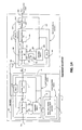
- FIG. 14 shows the block diagram of the cascaded equalizer 90 .
- the symbol a k required in the adaptation algorithm for the equalizer 2 1060 is replaced by the detected data symbol a k d provided by the BMAEHS.
- the symbol a k required in the adaptation algorithm for the equalizer 2 is replaced by the detected data symbol 2 a k d at the output of equalizer 2 .
- the detected data 2 a k d at the output of the equalizer 2 is expected to be more accurate than a k d .
- the performance of the cascaded equalizer may be considered to be equivalent to that of the single BMAEHS equalizer with equalizer parameter vector size N+N′ but with significantly much smaller computational requirements.
- the adaptation algorithm for the equalizer 2 may, for example, be selected to be the LMS, RLS or QS algorithm without the need for hierarchical structure of the algorithm.
- the stage 2 equalizer may also be a BMAEHS operating on the unknown channel with impulse response vector g k .
- the normalized channel output 8 z k+K 1 is input to the BMAEHS block 60 that provides the detected symbol 12 a k+M 1 d at the output.
- the detected data symbol 12 a k+M 1 d and the linear estimate of data symbol 10 â k+M 1 that is equal to 1008 2 z k+K 1 are inputted to the blind mode adaptive equalizer 2 1060 .
- the equalizer 2 1009 may be a decision feedback equalizer.
- the state vector 1014 of equalizer 2 1009 given by 2 ⁇ k [ 2 z k+M 1 , . . . , 2 z k+M 1 ⁇ N′ 1 , . . . , 2 z k+M 1 ⁇ N′+1 ] T is input to the adaptation block 2 1016 of the blind mode adaptive equalizer 2 1060 .
- the block diagram of the adaptation block 2 1016 of the blind mode adaptive equalizer 2 1060 is similar to that of adaptation block 16 given by FIG. 6 with the second correction signal vector w c 2 in the figure possibly set to 0.
- the iteration in (91a) is performed by the adaptation block 1016 for k> ⁇ 0.
- the convergence period N d is the time taken by the equalizer in the BMAEHS 60 to achieve some relatively small mean square error after the first N 1 samples of the normalized channel output is inputted into the equalizer and may be selected to be about 100-200 samples.
- the convergence period N′ d of the blind mode adaptive equalizer 2 1060 is similarly defined.
- the linear estimate 1010 of the data symbol â k+M 1 ⁇ N′ 1 is input to the decision device 1011 that provides the second detected data symbol 1012 2 a k+M 1 ⁇ N′ 1 d at the output of the device according to the decision function D( ) that may be given by (20)-(25).
- the detected data symbol 1012 2 a k+M 1 ⁇ N′ 1 d is connected to the input 2 of the switch S 4 1026 .
- the detected data symbol 12 a k+M 1 d from the BMAEHS 60 is inputted to the delay 1013 that provides a delayed version 1018 of the detected data symbol a k+M 1 ⁇ N′ 1 to the position 1 of the switch S 4 1026 .
- the output 1040 of the switch S 4 1026 is connected to the position 1 of the switch S 4 1026 for k+M 1 ⁇ N d +N′ 1 +N′ d and is in position 2 for k+M 1 ⁇ N d +N′ 1 +N′ d .
- the output 1040 a k+M 1 ⁇ N′ 1 of the switch S 4 1026 is the final detected output of the cascaded equalizer.
- the final detected symbol 1040 of the cascaded equalizer is equal to the delayed version 1018 of the detected symbol a k+M 1 ⁇ N′ 1 d from the BMAEHS 60 for k+M 1 ⁇ N d +N′ 1 +N′ d and is equal to the second detected data symbol 1012 2 a k+M 1 ⁇ N′ 1 d for k+M 1 ⁇ N d +N′ 1 +N′ d and is based on the combined equalization from both the stage 1 BMAEHS 60 and the stage 2 blind mode adaptive equalizer 2 1060 of the cascaded equalizer.
- the final detected symbol 1040 is inputted to the adaptation block 2 1016 and to the delay 1030 .
- the output 1032 of the delay is inputted to the equalizer filter 2 1009 .
- FIG. 15 shows the embodiment of the invention for the problem of adaptive digital beam former.
- a source transmitter 1210 inputs an RF signal obtained by the baseband to RF conversion, not shown, of the source data symbols a k to the transmit antenna 1215 for transmission.
- the transmitted RF signal is received by an array of N antennas 1202 a . . . n.
- the outputs 1222 of the antennas 1220 v R,1 (t), . . . , v R,N (t) are input to the N RF front end blocks 1225 a, . . . , n.
- the outputs 1226 of the N front end blocks v RF,1 (t), . . . , v RF,N (t) are inputted to the respective N RF to baseband complex converters 1230 a, . . . , n.
- the complex baseband signals 1232 v 1,k , . . . , v N,k are inputted to the adaptive digital beam former 1270 that provides the detected source data symbols a k d at the output.
- the complex baseband signals 1232 v 1,k , . . . , v N,k are inputted to the N multipliers 1235 a . . . n.
- n multiply the inputs by the respective weights ⁇ 1,k m , . . . , ⁇ N,k m made available by the multilevel adaptation block 1280 .
- the outputs 1236 of the multipliers z 1,k , . . . , z N,k are summed by the adder 1238 providing the signal 1239 s k at the output.
- the adder output 1239 s k is inputted to the combiner gain normalizer block 1250 providing the linear estimate of the data symbol 1252 â k to the decision device.
- the block diagram of the combiner gain normalizer block 1250 is similar to that of the channel gain normalizer 7 of FIG. 1 , except that the input z k c to the block 7 is replaced by the input 1239 s k .
- the decision device is similar to that given by the block 11 of FIG. 1 .
- the multilevel adaptation block 1280 generates the first correction signal vector w k c 1 to minimize the error between â k and a k d by minimizing the function
- I 1 ⁇ E ⁇ [ ⁇ a k d - a ⁇ k ⁇ 2 ] ( 92 )
- G k m is the modified gain estimate obtained by the combiner gain normalizer 1250
- v k [v 1,k , v 2,k , . . . , v N,k ] T
- ⁇ k b [ ⁇ 1,k b , . . . , ⁇ N,k b ] T is the beam former weight vector.
- the second correction signal vector w k c 2 is derived on the basis of the model error.
- In (97) g [g 1,k , g 2,k , . . . , g N,k ] T is a scalar gain times the antenna array direction vector and n k is the noise vector.
- K k is the Kalman gain matrix
- P k is the filter error covariance matrix
- R k denotes the covariance matrix of the noise vector n k appearing in (97)
- ⁇ is the exponential data weighting coefficient with 0 ⁇ 1.
- R k is an (N ⁇ N) matrix with possibly nonzero off diagonal elements when the noise n k is spatially correlated.
- P 0 selected to be a diagonal matrix
- R k a diagonal matrix
- P k from (101c) is also diagonal for all k>0.
- the robustness of the adaptive beam former may be further increased by simultaneously maximizing the signal to noise power ratio at the combiner output by maximizing the signal power at the output of the combiner while keeping the norm of the combiner weight vector ⁇ k close to 1. Equivalently the objective function I 3 given by (103) is minimized with respect to ⁇ k .
- I 3 1 2 ⁇ ⁇ ⁇ ( 1 - ⁇ w _ ⁇ k ⁇ 2 ) 2 - E ⁇ [ ⁇ w _ ⁇ T ⁇ v _ k ⁇ 2 ] ( 103 )
- ⁇ I 3 ⁇ w _ ⁇ k ⁇ ⁇ ( 1 - ⁇ w _ ⁇ k ⁇ 2 ) ⁇ w _ ⁇ k * - E ⁇ [ v _ k ⁇ a ⁇ * ] ( 104 )
- w k c 3 v k â* ⁇ ( 1 ⁇ ⁇ k ⁇ 2 ) ⁇ k * (105)
- ⁇ k+1 b ⁇ k+1 /G k m ;k
- the architecture of the beam former can also be applied to the problem of diversity combining.
- the level 1 adaptive system of FIG. 1 can be modified to include the constant modulus algorithm in those cases where the data symbol have constant modulus to provide additional robustness to the CMA based equalizers.
- the adaptive digital beam former architecture can be generalized to the case of broadband source wherein the various antenna gains and combiner weights are replaced by digital filters similar to the equalizer filter 9 of FIG. 1 .
- the equalizer architectures of the invention can be readily modified and applied to various fields where an equalizer or combiner architecture is applicable but without the requirements of any training sequences. Examples of such fields include radio astronomy, seismology, digital audio signal processing and so on.
- FIG. 1 may be implemented in many different embodiments of software, firmware, and/or hardware, for example, based on Field Programmable Gate Array (FPGA) chips or implemented in Application Specific Integrated Circuits (ASICS).
- the software and firmware code may be executed by a computer or computing device comprising a processor (e.g., a DSP or any other similar processing circuit) including, for example, the computing device 1600 described below.
- the processor may be in communication with memory or another computer readable medium comprising the software code.
- the software code or specialized control hardware that may be used to implement embodiments is not limiting.
- embodiments described herein may be implemented in computer software using any suitable computer software language type, using, for example, conventional or object-oriented techniques.
- Such software may be stored on any type of suitable computer-readable medium or media, such as, for example, a magnetic or optical storage medium.
- the software may be firmware stored at an EEPROM and/or other non-volatile memory associated a DSP or other similar processing circuit.
- the operation and behavior of the embodiments may be described without specific reference to specific software code or specialized hardware components. The absence of such specific references is feasible, because it is clearly understood that artisans of ordinary skill would be able to design software and control hardware to implement the embodiments based on the present description with no more than reasonable effort and without undue experimentation.
- FIG. 16 shows an example of a computing device 1600 according to one embodiment.
- the computing device 1600 is illustrated and described here in the context of a single computing device.
- any number of suitably configured computing devices can be used to implement a described embodiment.
- multiple communicatively linked computing devices may be used.
- One or more of these devices can be communicatively linked in any suitable way such as via one or more networks.
- One or more networks can include, without limitation: the Internet, one or more local area networks (LANs), one or more wide area networks (WANs) or any combination thereof.
- the computing device 1600 comprises one or more processor circuits or processing units 1602 , one or more memory circuits and/or storage circuit component(s) 1604 and one or more input/output (I/O) circuit devices 1606 .
- the computing device 1600 comprises a bus 1608 that allows the various circuit components and devices to communicate with one another.
- the bus 1608 represents one or more of any of several types of bus structures, including a memory bus or memory controller, a peripheral bus, an accelerated graphics port, and a processor or local bus using any of a variety of bus architectures.
- the bus 1608 may comprise wired and/or wireless buses.
- the processing unit 1602 may be responsible for executing various software programs such as system programs, applications programs, and/or program modules/blocks to provide computing and processing operations for the computing device 1600 .
- the processing unit 1602 may be responsible for performing various voice and data communications operations for the computing device 1600 such as transmitting and receiving voice and data information over one or more wired or wireless communications channels.
- the processing unit 1602 of the computing device 1600 is shown in the context of a single processor architecture, it may be appreciated that the computing device 1600 may use any suitable processor architecture and/or any suitable number of processors in accordance with the described embodiments. In one embodiment, the processing unit 1602 may be implemented using a single integrated processor.
- the processing unit 1602 may be implemented as a host central processing unit (CPU) using any suitable processor circuit or logic device (circuit), such as a as a general purpose processor.
- the processing unit 1602 also may be implemented as a chip multiprocessor (CMP), dedicated processor, embedded processor, media processor, input/output (I/O) processor, co-processor, microprocessor, controller, microcontroller, application specific integrated circuit (ASIC), field programmable gate array (FPGA), programmable logic device (PLD), or other processing device in accordance with the described embodiments.
- CMP chip multiprocessor
- dedicated processor dedicated processor
- embedded processor media processor
- I/O input/output
- co-processor co-processor
- microprocessor controller
- microcontroller application specific integrated circuit
- FPGA field programmable gate array
- PLD programmable logic device
- the processing unit 1602 may be coupled to the memory and/or storage component(s) 1604 through the bus 1608 .
- the bus 1608 may comprise any suitable interface and/or bus architecture for allowing the processing unit 1602 to access the memory and/or storage component(s) 1604 .
- the memory and/or storage component(s) 1604 may be shown as being separate from the processing unit 1602 for purposes of illustration, it is worthy to note that in various embodiments some portion or the entire memory and/or storage component(s) 1604 may be included on the same integrated circuit as the processing unit 1602 .
- some portion or the entire memory and/or storage component(s) 1604 may be disposed on an integrated circuit or other medium (e.g., hard disk drive) external to the integrated circuit of the processing unit 1602 .
- the computing device 1600 may comprise an expansion slot to support a multimedia and/or memory card, for example.
- the memory and/or storage component(s) 1604 represent one or more computer-readable media.
- the memory and/or storage component(s) 1604 may be implemented using any computer-readable media capable of storing data such as volatile or non-volatile memory, removable or non-removable memory, erasable or non-erasable memory, writeable or re-writeable memory, and so forth.
- the memory and/or storage component(s) 1604 may comprise volatile media (e.g., random access memory (RAM)) and/or nonvolatile media (e.g., read only memory (ROM), Flash memory, optical disks, magnetic disks and the like).
- volatile media e.g., random access memory (RAM)
- nonvolatile media e.g., read only memory (ROM), Flash memory, optical disks, magnetic disks and the like.
- the memory and/or storage component(s) 1604 may comprise fixed media (e.g., RAM, ROM, a fixed hard drive, etc.) as well as removable media (e.g., a Flash memory drive, a removable hard drive, an optical disk).
- Examples of computer-readable storage media may include, without limitation, RAM, dynamic RAM (DRAM), Double-Data-Rate DRAM (DDRAM), synchronous DRAM (SDRAM), static RAM (SRAM), read-only memory (ROM), programmable ROM (PROM), erasable programmable ROM (EPROM), electrically erasable programmable ROM (EEPROM), flash memory (e.g., NOR or NAND flash memory), content addressable memory (CAM), polymer memory (e.g., ferroelectric polymer memory), phase-change memory, ovonic memory, ferroelectric memory, silicon-oxide-nitride-oxide-silicon (SONOS) memory, magnetic or optical cards, or any other type of media suitable for storing information.
- RAM random access memory
- DRAM dynamic RAM
- DDRAM Double-Data-Rate DRAM
- SDRAM synchronous DRAM
- SRAM static RAM
- ROM read-only memory
- PROM programmable ROM
- EPROM erasable programmable ROM
- the one or more I/O devices 1606 allow a user to enter commands and information to the computing device 1600 , and also allow information to be presented to the user and/or other components or devices.
- input devices include data ports, analog to digital converters (ADCs), digital to analog converters (DACs), a keyboard, a cursor control device (e.g., a mouse), a microphone, a scanner and the like.
- output devices include data ports, ADC's, DAC's, a display device (e.g., a monitor or projector, speakers, a printer, a network card).
- the computing device 1600 may comprise an alphanumeric keypad coupled to the processing unit 1602 .
- the keypad may comprise, for example, a QWERTY key layout and an integrated number dial pad.
- the computing device 1600 may comprise a display coupled to the processing unit 1602 .
- the display may comprise any suitable visual interface for displaying content to a user of the computing device 1600 .
- the display may be implemented by a liquid crystal display (LCD) such as a touch-sensitive color (e.g., 76-bit color) thin-film transistor (TFT) LCD screen.
- LCD liquid crystal display
- TFT thin-film transistor
- the touch-sensitive LCD may be used with a stylus and/or a handwriting recognizer program.
- the processing unit 1602 may be arranged to provide processing or computing resources to the computing device 1600 .
- the processing unit 1602 may be responsible for executing various software programs including system programs such as operating system (OS) and application programs.
- System programs generally may assist in the running of the computing device 1600 and may be directly responsible for controlling, integrating, and managing the individual hardware components of the computer system.
- the OS may be implemented, for example, as a Microsoft® Windows OS, Symbian OSTM, Embedix OS, Linux OS, Binary Run-time Environment for Wireless (BREW) OS, JavaOS, or other suitable OS in accordance with the described embodiments.
- the computing device 1600 may comprise other system programs such as device drivers, programming tools, utility programs, software libraries, application programming interfaces (APIs), and so forth.
- APIs application programming interfaces
- a single component may be replaced by multiple components and multiple components may be replaced by a single component to perform a given function or functions. Except where such substitution would not be operative, such substitution is within the intended scope of the embodiments.
Abstract
Description
In (1) T denotes matrix transpose. The output of the discrete-time channel is given by the convolution of the input data symbol sequence ak with the channel impulse response
In (2a), H denotes the matrix conjugate transpose operation and * denotes the complex conjugate operation.
In (3) K1=
z k
In (4)
θr,k =D p(θb,k)=φi;φt
In (7) the mod 2π operation is defined as
ζk
In (9) the initial value of the accumulator output ζ−1 a is set equal to 0, and λP, 0<λp≦1, is a constant that determines the effective period of accumulation in the limit as k0→∞ and is approximately equal to 1/(1−λp), for example, λP may be selected equal to 0.998. Referring to
κk
|z| c =|z r |+j|z i |;z=z r +jz i ;j=√{square root over (−1)};z r ,z ireal (11)
of the
The output νk s of the
The output ν| a of the averaging
E[|a k|
For example, when both aI,k and aQ,k take possible values ±A0 and ±3A0 with equiprobable distribution, then
E[|a k|
α|=α|−1+μa e | m;|=1,2, . . . ;α0=1 (16)
αk=√{square root over ((1−d 2))} (18)
In equation (19) μa is some small positive constant and αo may be set to 1.
D(â I,k +jâ Q,k)=D I(â I,k)+jD Q(â Q,k) (20)
D I(x)=D I(x)=D m(|x|)sgn(x) (21)
D m(|x|)=iA 0 ;V t
D(â I,k +jâ Q,k)=sgn(â I,k)+jsgn(â Q,k) (25)
e k(a k+M
may provide a measure of the modeling error incurred by the
with respect to the equalizer parameter vector
R k=λ− [R k−1 −R k−1
With Rk in (30b) updated according to (29b). The algorithm in (30) may result in a faster convergence compared to that in (27).
R k q=λ−1 [R k−1 q −R k−1 q
The vector
ψk,i q =sgn(Re(ψk,i))+jsgn(Im(ψk,i));j=√{square root over (−1)};i=−N1, . . . , 0, . . . ,N 1 (31c)
In (31c) sgn(x) for x real is the signum function defined in (22), and Re(z) and Im(z) denote the real and imaginary components of z for any complex variable z.
z k =y k +n k; (32a)
where hi, −M1, . . . , 0, . . . , M1, are the components of the channel impulse response vector
In (33) the exponential data weighting coefficient λ is a constant taking values in the
The exponential data weighted least squares (LS) algorithm is obtained by setting the gradient in (34) equal to zero and is given by
In (35b) P−1 −1=εI for some small positive scalars ε and with I denoting the identity matrix. Alternatively, the use of the matrix inversion lemma yields the following recursive least squares (RLS) algorithm
P k=λ−1 [P k−1 −P k−1
In(36) the estimate
K k =P k−1
P k=λ−1 [P k11 −P k−1
The equations (37a)-(37c) may be initialized at k=0 with similar initialization as for the RLS algorithm of (36). Equations (37a) and (37b) may be combined into the following equivalent form
In equations (37b)-(37d), rk rk=2σ2 denotes the variance of the noise nk in (32a) equal to the noise nk c normalized by the modified channel gain Gk m.
P k q=λ−1 [P k−1 q −P k−1 q
where in (38)
Referring to
The resulting modified RLS algorithm is given by
P k=λ−1 [P k11 −P k−1
The elements of the vector k are obtained by the discrete convolution of the sequences {h−M
With N1>M1 as is usually the case, the K×N matrix H in (42) may be written in the following partitioned form
In (43) OM×(N−M) denotes M×(N−M) matrix with all its elements equal to zero and
For the case of non singular matrix H, this can be achieved by the selection of
However, for the more general case the equalizer parameter vector
J L
where ∥ ∥L
with δj denoting the jth component of the vector
Computationally the Euclidean norm L2 is most convenient and is given by
Equivalently the optimization function in (48) may be expressed in the following equivalent form
J 2=(H
The gradient of l2 with respect to the equalizer parameter vector
∂J 2 /∂
An iterative algorithm to minimize the objective function l2 is given by
with an appropriate initialization for
In (52) κ1 and κ2 are some positive constants determining the relative weights assigned to JL
From (53), the gradient vector of JL
In (54) the nth power of any vector
In (55b)
In (56) Ĥk is given by (44d) with hi replaced by its estimate ĥi,k for i=−M1, . . . , 0, . . . , M1. In various other embodiments of the invention, the second correction signal vector
An equivalent form for the update of the equalizer parameter vector
In (59) the operator Tr denotes the truncation of the vector to length N by deleting (M−1) elements from each side of the vector appearing in its argument. In (59b)
In various alternative embodiments of the invention, second correction signal vector
In (61a)
In (62) the product 2σ2∥
The power of the total distortion at the output of the equalizer is given by
and to minimize the total distortion σt 2, the constants κ1 and κ3 are related by κ1=E[|ak|2]κ3. With the modified optimization function in (62), the iterative algorithm in (60) is modified to
In (65) the parameter μ0 with 0≦μ0<1, is determined by the relative weight κ3. In various alternative embodiments of the invention, the second correction signal vector
In (66)
Similarly a vector
For the sake of notational simplification, the suffix k denoting the time index has been dropped from the elements of the vector
where in (69), the operator Φ denotes the (N+M+2) point discrete Fourier transform of its argument. For any vector
Where δN is the N×N matrix given by
with □ denoting the component wise multiplication, then the inverse discrete Fourier transform (IDFT) of
The inverse DFT of (
From (71)-(73) the IDFT of the product of
In (74) the symbol * on the right hand side of the equation denotes the elements that are irrelevant and the remaining elements are the same as the ones obtained by the conjugate of the convolution of
Tr 1(
The truncation operation Tr1 comprised of deleting (M−1) elements from each side of the vector in its argument on the left hand side of (75) is equivalent to deleting the last (M+2) elements from the vector on the right hand side of (74). From (74)-(75), a parameter update algorithm equivalent to (65a) for the case of κ=0 is given by
In (76) the truncation operation Tr2 is comprised of discarding the last (M+2) elements from the vector in its argument and in (77)
where
and is equal to the (K1+2)th row of the matrix ΓK defined by (70b) with N replaced by (K+3). In (78a)
In (79)
to the conjugate block 762. The
In (80) the dimension N of the equalizer parameter vector
In (82a) Ĥk + is an (M+N1)×(N1+1) matrix and is obtained from the matrix H+ with the elements hi of the matrix H+ replaced by the estimates ĥi,k for i=M1, . . . , 0, . . . , M1 and with the matrix H+ given by (83).
In (83b, c) 2M1 is assumed to be greater than N1. More generally the matrix H+ is obtained by N+M1 shifted versions of the channel impulse response vector
J L
with respect to the equalizer parameter vector
In (84b) O(K
With
In (86c)
may provide a measure of the modeling error incurred by the equalizer. A large deviation of the convolved response
K k e =Q k
Q k=λJ −1 [Q k−1 −Q k−1
The
p k a=λc p k−1 a +p k ;p −1 a =c 1 ;p k =∥
where λc with 0<λ≦1 is the exponential data weighting coefficient. The
κk=λcκk−1+1;κk=(1−λc)/(1−λc k) (89b)
The outputs of the accumulators Acc1 960 and
q k a=λc q k−1 a +q k ;q −1 a =c 2 ;q k =∥
p k f =p k a(1−λc)/(1−λc k);q k f =q k a(1−λc)/(1−λc k) (89d)
μd=μ0/√{square root over (p k f)};μ0/√{square root over (q k d)} (90)
with pk f and qk f evaluated according to (89). In (90) μ0 is some positive scalar.
where Gk m is the modified gain estimate obtained by the
|1 =E[|a k d −
where
From (95) the first correction signal vector wk c
w k c
In (97)
â k =
Thus ignoring the noise term in (8) the linear estimate of the data symbol âk will be equal to âk if
|2 =E[|1−
The gradient of I2 with respect to
Replacing ak by ak d in (97) results in the following exponentially data weighted Kalman filter algorithm for the estimate of
K k =P k−1 a k(|a k|2 P k−1 +λR k)−1 =P k a k R k −1 (101b)
P k=λ−1 [P k−1 −|a k|2 P k−1(|a k|2 P k−1 +λR k)−1 P k−1] (101c)
In (101)
Replacing
From (104), a third correction signal vector is given by
The update algorithm implemented by the
with the combiner gain Gk m inputted by
Claims (71)
Priority Applications (2)
| Application Number | Priority Date | Filing Date | Title |
|---|---|---|---|
| US13/434,498 US8711919B2 (en) | 2012-03-29 | 2012-03-29 | Systems and methods for adaptive blind mode equalization |
| US14/084,503 US9094253B2 (en) | 2012-03-29 | 2013-11-19 | Systems and methods for adaptive blind mode equalization |
Applications Claiming Priority (1)
| Application Number | Priority Date | Filing Date | Title |
|---|---|---|---|
| US13/434,498 US8711919B2 (en) | 2012-03-29 | 2012-03-29 | Systems and methods for adaptive blind mode equalization |
Related Child Applications (1)
| Application Number | Title | Priority Date | Filing Date |
|---|---|---|---|
| US14/084,503 Division US9094253B2 (en) | 2012-03-29 | 2013-11-19 | Systems and methods for adaptive blind mode equalization |
Publications (2)
| Publication Number | Publication Date |
|---|---|
| US20130259113A1 US20130259113A1 (en) | 2013-10-03 |
| US8711919B2 true US8711919B2 (en) | 2014-04-29 |
Family
ID=49235001
Family Applications (2)
| Application Number | Title | Priority Date | Filing Date |
|---|---|---|---|
| US13/434,498 Expired - Fee Related US8711919B2 (en) | 2012-03-29 | 2012-03-29 | Systems and methods for adaptive blind mode equalization |
| US14/084,503 Expired - Fee Related US9094253B2 (en) | 2012-03-29 | 2013-11-19 | Systems and methods for adaptive blind mode equalization |
Family Applications After (1)
| Application Number | Title | Priority Date | Filing Date |
|---|---|---|---|
| US14/084,503 Expired - Fee Related US9094253B2 (en) | 2012-03-29 | 2013-11-19 | Systems and methods for adaptive blind mode equalization |
Country Status (1)
| Country | Link |
|---|---|
| US (2) | US8711919B2 (en) |
Cited By (50)
| Publication number | Priority date | Publication date | Assignee | Title |
|---|---|---|---|---|
| US9053431B1 (en) | 2010-10-26 | 2015-06-09 | Michael Lamport Commons | Intelligent control with hierarchical stacked neural networks |
| US9288089B2 (en) | 2010-04-30 | 2016-03-15 | Ecole Polytechnique Federale De Lausanne (Epfl) | Orthogonal differential vector signaling |
| US9361223B1 (en) | 2012-05-14 | 2016-06-07 | Kandou Labs, S.A. | Storage method and apparatus for random access memory using codeword storage |
| US9362962B2 (en) | 2010-05-20 | 2016-06-07 | Kandou Labs, S.A. | Methods and systems for energy-efficient communications interface |
| US9424908B2 (en) | 2010-12-30 | 2016-08-23 | Kandou Labs, S.A. | Differential vector storage for dynamic random access memory |
| US9450791B2 (en) | 2010-05-20 | 2016-09-20 | Kandoub Lab, S.A. | Circuits for efficient detection of vector signaling codes for chip-to-chip communication |
| US9485057B2 (en) | 2010-05-20 | 2016-11-01 | Kandou Labs, S.A. | Vector signaling with reduced receiver complexity |
| US9544015B2 (en) | 2014-06-25 | 2017-01-10 | Kandou Labs, S.A. | Multilevel driver for high speed chip-to-chip communications |
| US9571306B2 (en) * | 2015-06-17 | 2017-02-14 | Mstar Semiconductor, Inc. | Device and method for eliminating channel effect |
| US9577664B2 (en) | 2010-05-20 | 2017-02-21 | Kandou Labs, S.A. | Efficient processing and detection of balanced codes |
| US9577815B1 (en) | 2015-10-29 | 2017-02-21 | Kandou Labs, S.A. | Clock data alignment system for vector signaling code communications link |
| US9607673B1 (en) | 2010-05-20 | 2017-03-28 | Kandou Labs S.A. | Methods and systems for pin-efficient memory controller interface using vector signaling codes for chip-to-chip communication |
| US9667379B2 (en) | 2010-06-04 | 2017-05-30 | Ecole Polytechnique Federale De Lausanne (Epfl) | Error control coding for orthogonal differential vector signaling |
| CN106797352A (en) * | 2014-07-10 | 2017-05-31 | 康杜实验室公司 | Noise eigen vector signaling code high |
| US9674014B2 (en) | 2014-10-22 | 2017-06-06 | Kandou Labs, S.A. | Method and apparatus for high speed chip-to-chip communications |
| US9686106B2 (en) | 2014-02-28 | 2017-06-20 | Kandou Labs, S.A. | Clock-embedded vector signaling codes |
| US9686107B2 (en) | 2010-05-20 | 2017-06-20 | Kandou Labs, S.A. | Methods and systems for chip-to-chip communication with reduced simultaneous switching noise |
| US9692381B2 (en) | 2014-05-16 | 2017-06-27 | Kandou Labs, S.A. | Symmetric linear equalization circuit with increased gain |
| US9825723B2 (en) | 2010-05-20 | 2017-11-21 | Kandou Labs, S.A. | Methods and systems for skew tolerance in and advanced detectors for vector signaling codes for chip-to-chip communication |
| US9832046B2 (en) | 2015-06-26 | 2017-11-28 | Kandou Labs, S.A. | High speed communications system |
| US9838017B2 (en) | 2010-05-20 | 2017-12-05 | Kandou Labs, S.A. | Methods and systems for high bandwidth chip-to-chip communcations interface |
| US9838234B2 (en) | 2014-08-01 | 2017-12-05 | Kandou Labs, S.A. | Orthogonal differential vector signaling codes with embedded clock |
| US9875440B1 (en) | 2010-10-26 | 2018-01-23 | Michael Lamport Commons | Intelligent control with hierarchical stacked neural networks |
| US9893911B2 (en) | 2014-07-21 | 2018-02-13 | Kandou Labs, S.A. | Multidrop data transfer |
| US9906358B1 (en) | 2016-08-31 | 2018-02-27 | Kandou Labs, S.A. | Lock detector for phase lock loop |
| US9985745B2 (en) | 2013-06-25 | 2018-05-29 | Kandou Labs, S.A. | Vector signaling with reduced receiver complexity |
| US10003424B2 (en) | 2014-07-17 | 2018-06-19 | Kandou Labs, S.A. | Bus reversible orthogonal differential vector signaling codes |
| US10003315B2 (en) | 2016-01-25 | 2018-06-19 | Kandou Labs S.A. | Voltage sampler driver with enhanced high-frequency gain |
| US10003454B2 (en) | 2016-04-22 | 2018-06-19 | Kandou Labs, S.A. | Sampler with low input kickback |
| US10056903B2 (en) | 2016-04-28 | 2018-08-21 | Kandou Labs, S.A. | Low power multilevel driver |
| US10057049B2 (en) | 2016-04-22 | 2018-08-21 | Kandou Labs, S.A. | High performance phase locked loop |
| US10055372B2 (en) | 2015-11-25 | 2018-08-21 | Kandou Labs, S.A. | Orthogonal differential vector signaling codes with embedded clock |
| US10091035B2 (en) | 2013-04-16 | 2018-10-02 | Kandou Labs, S.A. | Methods and systems for high bandwidth communications interface |
| US10116468B1 (en) | 2017-06-28 | 2018-10-30 | Kandou Labs, S.A. | Low power chip-to-chip bidirectional communications |
| US10153591B2 (en) | 2016-04-28 | 2018-12-11 | Kandou Labs, S.A. | Skew-resistant multi-wire channel |
| US10177812B2 (en) | 2014-01-31 | 2019-01-08 | Kandou Labs, S.A. | Methods and systems for reduction of nearest-neighbor crosstalk |
| US10200188B2 (en) | 2016-10-21 | 2019-02-05 | Kandou Labs, S.A. | Quadrature and duty cycle error correction in matrix phase lock loop |
| US10200218B2 (en) | 2016-10-24 | 2019-02-05 | Kandou Labs, S.A. | Multi-stage sampler with increased gain |
| US10203226B1 (en) | 2017-08-11 | 2019-02-12 | Kandou Labs, S.A. | Phase interpolation circuit |
| US10277431B2 (en) | 2016-09-16 | 2019-04-30 | Kandou Labs, S.A. | Phase rotation circuit for eye scope measurements |
| US10326623B1 (en) | 2017-12-08 | 2019-06-18 | Kandou Labs, S.A. | Methods and systems for providing multi-stage distributed decision feedback equalization |
| US10333749B2 (en) | 2014-05-13 | 2019-06-25 | Kandou Labs, S.A. | Vector signaling code with improved noise margin |
| US10333741B2 (en) | 2016-04-28 | 2019-06-25 | Kandou Labs, S.A. | Vector signaling codes for densely-routed wire groups |
| US10348436B2 (en) | 2014-02-02 | 2019-07-09 | Kandou Labs, S.A. | Method and apparatus for low power chip-to-chip communications with constrained ISI ratio |
| US10372665B2 (en) | 2016-10-24 | 2019-08-06 | Kandou Labs, S.A. | Multiphase data receiver with distributed DFE |
| US10554380B2 (en) | 2018-01-26 | 2020-02-04 | Kandou Labs, S.A. | Dynamically weighted exclusive or gate having weighted output segments for phase detection and phase interpolation |
| US10666297B2 (en) | 2017-04-14 | 2020-05-26 | Kandou Labs, S.A. | Pipelined forward error correction for vector signaling code channel |
| US10686583B2 (en) | 2017-07-04 | 2020-06-16 | Kandou Labs, S.A. | Method for measuring and correcting multi-wire skew |
| US10693587B2 (en) | 2017-07-10 | 2020-06-23 | Kandou Labs, S.A. | Multi-wire permuted forward error correction |
| US11356197B1 (en) | 2021-03-19 | 2022-06-07 | Kandou Labs SA | Error-tolerant forward error correction ordered set message decoder |
Families Citing this family (48)
| Publication number | Priority date | Publication date | Assignee | Title |
|---|---|---|---|---|
| US8670390B2 (en) * | 2000-11-22 | 2014-03-11 | Genghiscomm Holdings, LLC | Cooperative beam-forming in wireless networks |
| US11381285B1 (en) | 2004-08-02 | 2022-07-05 | Genghiscomm Holdings, LLC | Transmit pre-coding |
| US9479369B1 (en) | 2010-05-20 | 2016-10-25 | Kandou Labs, S.A. | Vector signaling codes with high pin-efficiency for chip-to-chip communication and storage |
| US9401828B2 (en) | 2010-05-20 | 2016-07-26 | Kandou Labs, S.A. | Methods and systems for low-power and pin-efficient communications with superposition signaling codes |
| US9596109B2 (en) | 2010-05-20 | 2017-03-14 | Kandou Labs, S.A. | Methods and systems for high bandwidth communications interface |
| US9450744B2 (en) | 2010-05-20 | 2016-09-20 | Kandou Lab, S.A. | Control loop management and vector signaling code communications links |
| CN102457459B (en) * | 2010-10-16 | 2016-06-08 | 中兴通讯股份有限公司 | A kind of complex carrier modulation method, Apparatus and system |
| WO2013115666A1 (en) * | 2012-01-30 | 2013-08-08 | Intel Corporation | Multi-mode frequency domain equalization with adaptation to varying channel conditions |
| US9252908B1 (en) | 2012-04-12 | 2016-02-02 | Tarana Wireless, Inc. | Non-line of sight wireless communication system and method |
| US9270304B2 (en) * | 2012-11-07 | 2016-02-23 | Datum Systems, Inc. | Method and apparatus for nonlinear-channel identification and estimation of nonlinear-distorted signals |
| US10499456B1 (en) | 2013-03-15 | 2019-12-03 | Tarana Wireless, Inc. | Distributed capacity base station architecture for broadband access with enhanced in-band GPS co-existence |
| US9785592B2 (en) * | 2014-01-22 | 2017-10-10 | Avago Technologies General Ip (Singapore) Pte. Ltd. | High density mapping for multiple converter samples in multiple lane interface |
| US10348394B1 (en) | 2014-03-14 | 2019-07-09 | Tarana Wireless, Inc. | System architecture and method for enhancing wireless networks with mini-satellites and pseudollites and adaptive antenna processing |
| US11240076B2 (en) | 2014-05-13 | 2022-02-01 | Kandou Labs, S.A. | Vector signaling code with improved noise margin |
| CN105337906B (en) * | 2014-07-24 | 2019-02-05 | 华为技术有限公司 | Channel estimation methods and device |
| US10383024B2 (en) * | 2015-03-10 | 2019-08-13 | Analog Devices, Inc. | System and method for efficient fronthaul communication for wireless communication |
| US9557760B1 (en) | 2015-10-28 | 2017-01-31 | Kandou Labs, S.A. | Enhanced phase interpolation circuit |
| TWI627846B (en) * | 2016-03-30 | 2018-06-21 | 晨星半導體股份有限公司 | Module of enhancing equalization, demodulation system and method of enhancing equalization |
| US10242749B2 (en) | 2016-04-22 | 2019-03-26 | Kandou Labs, S.A. | Calibration apparatus and method for sampler with adjustable high frequency gain |
| US10193716B2 (en) | 2016-04-28 | 2019-01-29 | Kandou Labs, S.A. | Clock data recovery with decision feedback equalization |
| US9985815B2 (en) * | 2016-08-25 | 2018-05-29 | Intel IP Corporation | Signal processing chain switching |
| CN106355908A (en) * | 2016-11-30 | 2017-01-25 | 深圳明创自控技术有限公司 | Intelligent control system for traffic lights based on cloud computing |
| CN106789457A (en) * | 2016-11-30 | 2017-05-31 | 深圳汇通智能化科技有限公司 | A kind of intelligent home control system based on Internet of Things |
| CN107070825B (en) * | 2017-04-07 | 2020-06-23 | 淮南联合大学 | Wavelet weighted multi-mode blind equalization method based on simulated annealing wolf pack optimization |
| US10693473B2 (en) | 2017-05-22 | 2020-06-23 | Kandou Labs, S.A. | Multi-modal data-driven clock recovery circuit |
| US10637705B1 (en) | 2017-05-25 | 2020-04-28 | Genghiscomm Holdings, LLC | Peak-to-average-power reduction for OFDM multiple access |
| US10425182B2 (en) | 2017-09-29 | 2019-09-24 | Futurewei Technologies, Inc. | Inter-band distortion and interference mitigation within communication systems |
| US10467177B2 (en) | 2017-12-08 | 2019-11-05 | Kandou Labs, S.A. | High speed memory interface |
| CN107967407B (en) * | 2017-12-19 | 2021-05-04 | 中国科学院上海天文台 | Radio astronomical data processing method |
| CN111684772B (en) | 2017-12-28 | 2023-06-16 | 康杜实验室公司 | Synchronous switching multiple-input demodulation comparator |
| US10950251B2 (en) * | 2018-03-05 | 2021-03-16 | Dts, Inc. | Coding of harmonic signals in transform-based audio codecs |
| US10374844B1 (en) * | 2018-03-08 | 2019-08-06 | Nxp B.V. | Signal-equalization with noise-whitening filter |
| US10615881B2 (en) * | 2018-03-23 | 2020-04-07 | Huawei Technologies Co., Ltd. | System and method for adaptive channel equalization in a time varying channel |
| EP3808044A1 (en) | 2018-06-12 | 2021-04-21 | Kandou Labs, S.A. | Passive multi-input comparator for orthogonal codes on a multi-wire bus |
| US10931249B2 (en) | 2018-06-12 | 2021-02-23 | Kandou Labs, S.A. | Amplifier with adjustable high-frequency gain using varactor diodes |
| KR102579595B1 (en) | 2018-09-10 | 2023-09-18 | 칸도우 랩스 에스에이 | Programmable continuous-time linear equalizer with stabilized high-frequency peaking to control the operating current of the slicer |
| CN111786669B (en) * | 2019-04-04 | 2023-09-12 | 智原微电子(苏州)有限公司 | Apparatus for adaptive control of decision feedback equalizer |
| US10608849B1 (en) | 2019-04-08 | 2020-03-31 | Kandou Labs, S.A. | Variable gain amplifier and sampler offset calibration without clock recovery |
| US10574487B1 (en) | 2019-04-08 | 2020-02-25 | Kandou Labs, S.A. | Sampler offset calibration during operation |
| US10721106B1 (en) | 2019-04-08 | 2020-07-21 | Kandou Labs, S.A. | Adaptive continuous time linear equalization and channel bandwidth control |
| US10680634B1 (en) | 2019-04-08 | 2020-06-09 | Kandou Labs, S.A. | Dynamic integration time adjustment of a clocked data sampler using a static analog calibration circuit |
| US11146439B2 (en) * | 2019-12-04 | 2021-10-12 | National Instruments Corporation | Robust carrier phase and frequency tracking for M-QAM demodulation |
| CN112787723B (en) * | 2020-12-29 | 2022-03-25 | 武汉邮电科学研究院有限公司 | Nonlinear encoder, encoding method and optical transmission system |
| US11303484B1 (en) | 2021-04-02 | 2022-04-12 | Kandou Labs SA | Continuous time linear equalization and bandwidth adaptation using asynchronous sampling |
| US11374800B1 (en) | 2021-04-14 | 2022-06-28 | Kandou Labs SA | Continuous time linear equalization and bandwidth adaptation using peak detector |
| US11456708B1 (en) | 2021-04-30 | 2022-09-27 | Kandou Labs SA | Reference generation circuit for maintaining temperature-tracked linearity in amplifier with adjustable high-frequency gain |
| CN113852383B (en) * | 2021-09-23 | 2022-08-09 | 上海航天电子通讯设备研究所 | Anti-interference processing system for VHF frequency band burst signals |
| US11831472B1 (en) | 2022-08-30 | 2023-11-28 | Kandou Labs SA | Pre-scaler for orthogonal differential vector signalling |
Citations (3)
| Publication number | Priority date | Publication date | Assignee | Title |
|---|---|---|---|---|
| US5918161A (en) | 1997-01-16 | 1999-06-29 | The United States Of America As Represented By The Administrator Of The National Aeronautics And Space Administration | Method and apparatus for reducing multipath signal error using deconvolution |
| US7421019B2 (en) * | 2004-06-18 | 2008-09-02 | Chung Shan Institute Of Science And Technology, Armaments Bureau, M.N.D. | Hierarchical adaptive equalizer and design method thereof |
| US20080260017A1 (en) | 2007-04-18 | 2008-10-23 | Mediatek Inc. | Selective slicing equalizer |
Family Cites Families (3)
| Publication number | Priority date | Publication date | Assignee | Title |
|---|---|---|---|---|
| US6275543B1 (en) * | 1996-10-11 | 2001-08-14 | Arraycomm, Inc. | Method for reference signal generation in the presence of frequency offsets in a communications station with spatial processing |
| KR100424496B1 (en) * | 2000-08-31 | 2004-03-26 | 삼성전자주식회사 | Method and apparatus for controlling equalizer using sync signal in digital vestigial sideband system |
| US7050419B2 (en) * | 2001-02-23 | 2006-05-23 | Terayon Communicaion Systems, Inc. | Head end receiver for digital data delivery systems using mixed mode SCDMA and TDMA multiplexing |
-
2012
- 2012-03-29 US US13/434,498 patent/US8711919B2/en not_active Expired - Fee Related
-
2013
- 2013-11-19 US US14/084,503 patent/US9094253B2/en not_active Expired - Fee Related
Patent Citations (3)
| Publication number | Priority date | Publication date | Assignee | Title |
|---|---|---|---|---|
| US5918161A (en) | 1997-01-16 | 1999-06-29 | The United States Of America As Represented By The Administrator Of The National Aeronautics And Space Administration | Method and apparatus for reducing multipath signal error using deconvolution |
| US7421019B2 (en) * | 2004-06-18 | 2008-09-02 | Chung Shan Institute Of Science And Technology, Armaments Bureau, M.N.D. | Hierarchical adaptive equalizer and design method thereof |
| US20080260017A1 (en) | 2007-04-18 | 2008-10-23 | Mediatek Inc. | Selective slicing equalizer |
Non-Patent Citations (18)
| Title |
|---|
| D. N. Godard, "Self Recovering Equalization and carrier Tracking in Two-Dimensional Data Communication Systems," IEEE Trans. On Communications, vol. com-28, Nov. 1980, pp. 1867-1875. |
| H.H. Zeng and L. Tong, "Blind Equalization Using the Constant Modulus Algorithm," Proceedings of ICSP, 96, pp. 400-403. |
| http://ens.ewi.tudelft.nl/Education/courses/et4147/sheets/cma-leus.pdf Constant Modulus Algorithm, T U Delft University, pp. 1-12. |
| http://ens.ewi.tudelft.nl/Education/courses/et4147/sheets/cma—leus.pdf Constant Modulus Algorithm, T U Delft University, pp. 1-12. |
| R. Kumar and J. B. Moore, "Adaptive Equalization via Fast Quantized State Methods," IEEE Transactions on Communications, vol. 29, Oct. 1981, pp. 1492 1501. |
| R. Kumar and J. B. Moore, "Detection Techniques in Least Squares Identification," Automatica, vol. 17, Nov. 1981, pp. 805 819. |
| R. Kumar and J. B. Moore, "State Inverse and Decorrelated State Stochastic Approximation," Automatica, vol. 16, May 1980, pp. 259 311. |
| R. Kumar and S. Jalali, "Super Fast and Efficient Channel Equalizer Architecture Based on Neural Network," IEEE International Conference on Aerospace Engineering, Big Sky, Montana, Mar. 2012, pp. 1-11. |
| R. Kumar, "Adaptive Algorithms for Antenna Array Signal Processing," Proceedings of the 31st Annual Conference on Information Sciences and Systems, John Hopkins University Baltimore, MD, Mar. 19-21, 1995, pp. 379-386. |
| R. Kumar, "Adaptive Algorithms for Antenna Array Signal Processing," U.S. Air Force Summer Research Program, 1993, Final Reports, pp. 5.1-5.31, Also on the website: http://www.dtic.mil/dtic/tr/fulltext/u2/a278695.pdf. |
| R. Kumar, "Convergence of Decision Directed Adaptive Equalizer," Proceedings of 22nd IEEE Conference on Decision and Control, San Antonio, Texas, Dec. 1983, pp. 1319 1324. |
| R. Kumar, "Multi Element Array Signal Reconstruction with Adaptive Least-Squares Algorithm," International Journal of Adaptive Control and Signal Processing, vol. 6, Dec. 1992, pp. 561-588. |
| R. R. Lopes and J.R. Barry, "Blind Iterative Channel Identification and Equalization," International Conference on Communication, Helsinki, Jun. 2001, pp. 2256-2260. |
| R.H. Lambert and C.L. Nikias, "Forward/Inverse Blind Equalization," 1994 Conference Record of the 28th Asilomar Conference on Signals, Systems and Computers, vol. 2, 1995. |
| S. Abrar, A. Zerguine and M. Deriche "Self-Orthogonalizing Soft Constraint Satisfaction Multi Modulus Blind Equalization Algorithms," Proc. IEEE International Conference on Acoustics Speech and Signal Processing, 2004, pp. II-853-II-856. |
| W. Chung and J.P. LeBlanc, "The Local Minima of Fractionally Spaced CMA Blind Equalizer Cost Function in the Presence of Channel Noise," Proc. IEEE International Conference on Acoustics Speech and Signal Processing, May 1998, pp. 3345-3348. |
| W. J. Weber, "Differential Encoding for Multiple Amplitude and Phase Shift Keying," IEEE Trans. On Communications, vol. com-26, Mar. 1978, pp. 385-391. |
| Y. Sato, "A Method for Self-Recovering Equalization for Multilevel Amplitude Modulation Systems," IEEE Trans. On Communications, vol. com-23, Jun. 1975, pp. 679-682. |
Cited By (79)
| Publication number | Priority date | Publication date | Assignee | Title |
|---|---|---|---|---|
| US10355756B2 (en) | 2010-04-30 | 2019-07-16 | ECOLE POLYTECHNIQUE FéDéRALE DE LAUSANNE | Orthogonal differential vector signaling |
| US9288089B2 (en) | 2010-04-30 | 2016-03-15 | Ecole Polytechnique Federale De Lausanne (Epfl) | Orthogonal differential vector signaling |
| US9825677B2 (en) | 2010-04-30 | 2017-11-21 | ECOLE POLYTECHNIQUE FéDéRALE DE LAUSANNE | Orthogonal differential vector signaling |
| US10468078B2 (en) | 2010-05-20 | 2019-11-05 | Kandou Labs, S.A. | Methods and systems for pin-efficient memory controller interface using vector signaling codes for chip-to-chip communication |
| US9825723B2 (en) | 2010-05-20 | 2017-11-21 | Kandou Labs, S.A. | Methods and systems for skew tolerance in and advanced detectors for vector signaling codes for chip-to-chip communication |
| US9450791B2 (en) | 2010-05-20 | 2016-09-20 | Kandoub Lab, S.A. | Circuits for efficient detection of vector signaling codes for chip-to-chip communication |
| US9485057B2 (en) | 2010-05-20 | 2016-11-01 | Kandou Labs, S.A. | Vector signaling with reduced receiver complexity |
| US10044452B2 (en) | 2010-05-20 | 2018-08-07 | Kandou Labs, S.A. | Methods and systems for skew tolerance in and advanced detectors for vector signaling codes for chip-to-chip communication |
| US9838017B2 (en) | 2010-05-20 | 2017-12-05 | Kandou Labs, S.A. | Methods and systems for high bandwidth chip-to-chip communcations interface |
| US9819522B2 (en) | 2010-05-20 | 2017-11-14 | Kandou Labs, S.A. | Circuits for efficient detection of vector signaling codes for chip-to-chip communication |
| US9577664B2 (en) | 2010-05-20 | 2017-02-21 | Kandou Labs, S.A. | Efficient processing and detection of balanced codes |
| US9692555B2 (en) | 2010-05-20 | 2017-06-27 | Kandou Labs, S.A. | Vector signaling with reduced receiver complexity |
| US9607673B1 (en) | 2010-05-20 | 2017-03-28 | Kandou Labs S.A. | Methods and systems for pin-efficient memory controller interface using vector signaling codes for chip-to-chip communication |
| US9686107B2 (en) | 2010-05-20 | 2017-06-20 | Kandou Labs, S.A. | Methods and systems for chip-to-chip communication with reduced simultaneous switching noise |
| US9362962B2 (en) | 2010-05-20 | 2016-06-07 | Kandou Labs, S.A. | Methods and systems for energy-efficient communications interface |
| US9667379B2 (en) | 2010-06-04 | 2017-05-30 | Ecole Polytechnique Federale De Lausanne (Epfl) | Error control coding for orthogonal differential vector signaling |
| US9053431B1 (en) | 2010-10-26 | 2015-06-09 | Michael Lamport Commons | Intelligent control with hierarchical stacked neural networks |
| US11868883B1 (en) | 2010-10-26 | 2024-01-09 | Michael Lamport Commons | Intelligent control with hierarchical stacked neural networks |
| US9875440B1 (en) | 2010-10-26 | 2018-01-23 | Michael Lamport Commons | Intelligent control with hierarchical stacked neural networks |
| US10510000B1 (en) | 2010-10-26 | 2019-12-17 | Michael Lamport Commons | Intelligent control with hierarchical stacked neural networks |
| US11514305B1 (en) | 2010-10-26 | 2022-11-29 | Michael Lamport Commons | Intelligent control with hierarchical stacked neural networks |
| US9424908B2 (en) | 2010-12-30 | 2016-08-23 | Kandou Labs, S.A. | Differential vector storage for dynamic random access memory |
| US10164809B2 (en) | 2010-12-30 | 2018-12-25 | Kandou Labs, S.A. | Circuits for efficient detection of vector signaling codes for chip-to-chip communication |
| US9361223B1 (en) | 2012-05-14 | 2016-06-07 | Kandou Labs, S.A. | Storage method and apparatus for random access memory using codeword storage |
| US9524106B1 (en) | 2012-05-14 | 2016-12-20 | Kandou Labs, S.A. | Storage method and apparatus for random access memory using codeword storage |
| US10091035B2 (en) | 2013-04-16 | 2018-10-02 | Kandou Labs, S.A. | Methods and systems for high bandwidth communications interface |
| US9985745B2 (en) | 2013-06-25 | 2018-05-29 | Kandou Labs, S.A. | Vector signaling with reduced receiver complexity |
| US10177812B2 (en) | 2014-01-31 | 2019-01-08 | Kandou Labs, S.A. | Methods and systems for reduction of nearest-neighbor crosstalk |
| US10348436B2 (en) | 2014-02-02 | 2019-07-09 | Kandou Labs, S.A. | Method and apparatus for low power chip-to-chip communications with constrained ISI ratio |
| US9686106B2 (en) | 2014-02-28 | 2017-06-20 | Kandou Labs, S.A. | Clock-embedded vector signaling codes |
| US10020966B2 (en) | 2014-02-28 | 2018-07-10 | Kandou Labs, S.A. | Vector signaling codes with high pin-efficiency for chip-to-chip communication and storage |
| US10333749B2 (en) | 2014-05-13 | 2019-06-25 | Kandou Labs, S.A. | Vector signaling code with improved noise margin |
| US9692381B2 (en) | 2014-05-16 | 2017-06-27 | Kandou Labs, S.A. | Symmetric linear equalization circuit with increased gain |
| US9544015B2 (en) | 2014-06-25 | 2017-01-10 | Kandou Labs, S.A. | Multilevel driver for high speed chip-to-chip communications |
| US10091033B2 (en) | 2014-06-25 | 2018-10-02 | Kandou Labs, S.A. | Multilevel driver for high speed chip-to-chip communications |
| US9917711B2 (en) | 2014-06-25 | 2018-03-13 | Kandou Labs, S.A. | Multilevel driver for high speed chip-to-chip communications |
| CN106797352B (en) * | 2014-07-10 | 2020-04-07 | 康杜实验室公司 | High signal-to-noise characteristic vector signaling code |
| CN106797352A (en) * | 2014-07-10 | 2017-05-31 | 康杜实验室公司 | Noise eigen vector signaling code high |
| US10320588B2 (en) | 2014-07-10 | 2019-06-11 | Kandou Labs, S.A. | Vector signaling codes with increased signal to noise characteristics |
| US10003424B2 (en) | 2014-07-17 | 2018-06-19 | Kandou Labs, S.A. | Bus reversible orthogonal differential vector signaling codes |
| US10404394B2 (en) | 2014-07-17 | 2019-09-03 | Kandou Labs, S.A. | Bus reversible orthogonal differential vector signaling codes |
| US10999106B2 (en) | 2014-07-21 | 2021-05-04 | Kandou Labs, S.A. | Multidrop data transfer |
| US10230549B2 (en) | 2014-07-21 | 2019-03-12 | Kandou Labs, S.A. | Multidrop data transfer |
| US9893911B2 (en) | 2014-07-21 | 2018-02-13 | Kandou Labs, S.A. | Multidrop data transfer |
| US9838234B2 (en) | 2014-08-01 | 2017-12-05 | Kandou Labs, S.A. | Orthogonal differential vector signaling codes with embedded clock |
| US10122561B2 (en) | 2014-08-01 | 2018-11-06 | Kandou Labs, S.A. | Orthogonal differential vector signaling codes with embedded clock |
| US9674014B2 (en) | 2014-10-22 | 2017-06-06 | Kandou Labs, S.A. | Method and apparatus for high speed chip-to-chip communications |
| US10243765B2 (en) | 2014-10-22 | 2019-03-26 | Kandou Labs, S.A. | Method and apparatus for high speed chip-to-chip communications |
| US9571306B2 (en) * | 2015-06-17 | 2017-02-14 | Mstar Semiconductor, Inc. | Device and method for eliminating channel effect |
| US10116472B2 (en) | 2015-06-26 | 2018-10-30 | Kandou Labs, S.A. | High speed communications system |
| US9832046B2 (en) | 2015-06-26 | 2017-11-28 | Kandou Labs, S.A. | High speed communications system |
| US9577815B1 (en) | 2015-10-29 | 2017-02-21 | Kandou Labs, S.A. | Clock data alignment system for vector signaling code communications link |
| US10324876B2 (en) | 2015-11-25 | 2019-06-18 | Kandou Labs, S.A. | Orthogonal differential vector signaling codes with embedded clock |
| US10055372B2 (en) | 2015-11-25 | 2018-08-21 | Kandou Labs, S.A. | Orthogonal differential vector signaling codes with embedded clock |
| US10003315B2 (en) | 2016-01-25 | 2018-06-19 | Kandou Labs S.A. | Voltage sampler driver with enhanced high-frequency gain |
| US10003454B2 (en) | 2016-04-22 | 2018-06-19 | Kandou Labs, S.A. | Sampler with low input kickback |
| US10057049B2 (en) | 2016-04-22 | 2018-08-21 | Kandou Labs, S.A. | High performance phase locked loop |
| US10153591B2 (en) | 2016-04-28 | 2018-12-11 | Kandou Labs, S.A. | Skew-resistant multi-wire channel |
| US10333741B2 (en) | 2016-04-28 | 2019-06-25 | Kandou Labs, S.A. | Vector signaling codes for densely-routed wire groups |
| US10056903B2 (en) | 2016-04-28 | 2018-08-21 | Kandou Labs, S.A. | Low power multilevel driver |
| US10355852B2 (en) | 2016-08-31 | 2019-07-16 | Kandou Labs, S.A. | Lock detector for phase lock loop |
| US9906358B1 (en) | 2016-08-31 | 2018-02-27 | Kandou Labs, S.A. | Lock detector for phase lock loop |
| US10277431B2 (en) | 2016-09-16 | 2019-04-30 | Kandou Labs, S.A. | Phase rotation circuit for eye scope measurements |
| US10200188B2 (en) | 2016-10-21 | 2019-02-05 | Kandou Labs, S.A. | Quadrature and duty cycle error correction in matrix phase lock loop |
| US10200218B2 (en) | 2016-10-24 | 2019-02-05 | Kandou Labs, S.A. | Multi-stage sampler with increased gain |
| US10372665B2 (en) | 2016-10-24 | 2019-08-06 | Kandou Labs, S.A. | Multiphase data receiver with distributed DFE |
| US11336302B2 (en) | 2017-04-14 | 2022-05-17 | Kandou Labs, S.A. | Pipelined forward error correction for vector signaling code channel |
| US10666297B2 (en) | 2017-04-14 | 2020-05-26 | Kandou Labs, S.A. | Pipelined forward error correction for vector signaling code channel |
| US11804855B2 (en) | 2017-04-14 | 2023-10-31 | Kandou Labs, S.A. | Pipelined forward error correction for vector signaling code channel |
| US10116468B1 (en) | 2017-06-28 | 2018-10-30 | Kandou Labs, S.A. | Low power chip-to-chip bidirectional communications |
| US10686583B2 (en) | 2017-07-04 | 2020-06-16 | Kandou Labs, S.A. | Method for measuring and correcting multi-wire skew |
| US10693587B2 (en) | 2017-07-10 | 2020-06-23 | Kandou Labs, S.A. | Multi-wire permuted forward error correction |
| US11368247B2 (en) | 2017-07-10 | 2022-06-21 | Kandou Labs, S.A. | Multi-wire permuted forward error correction |
| US11894926B2 (en) | 2017-07-10 | 2024-02-06 | Kandou Labs, S.A. | Interleaved forward error correction over multiple transport channels |
| US10203226B1 (en) | 2017-08-11 | 2019-02-12 | Kandou Labs, S.A. | Phase interpolation circuit |
| US10326623B1 (en) | 2017-12-08 | 2019-06-18 | Kandou Labs, S.A. | Methods and systems for providing multi-stage distributed decision feedback equalization |
| US10554380B2 (en) | 2018-01-26 | 2020-02-04 | Kandou Labs, S.A. | Dynamically weighted exclusive or gate having weighted output segments for phase detection and phase interpolation |
| US11356197B1 (en) | 2021-03-19 | 2022-06-07 | Kandou Labs SA | Error-tolerant forward error correction ordered set message decoder |
| US11658771B2 (en) | 2021-03-19 | 2023-05-23 | Kandou Labs SA | Error-tolerant forward error correction ordered set message decoder |
Also Published As
| Publication number | Publication date |
|---|---|
| US20130259113A1 (en) | 2013-10-03 |
| US20140140387A1 (en) | 2014-05-22 |
| US9094253B2 (en) | 2015-07-28 |
Similar Documents
| Publication | Publication Date | Title |
|---|---|---|
| US8711919B2 (en) | Systems and methods for adaptive blind mode equalization | |
| US7787556B2 (en) | Method and apparatus for signal detection and matrix decomposition | |
| JP6271042B2 (en) | System and method for recovering carrier phase in optical communications | |
| EP2375660B1 (en) | Symbol de-mapping methods in multiple-input multiple-output systems | |
| CN107431538B (en) | The method and receiver be decoded to optical signal | |
| US7457367B2 (en) | Detector and method for estimating data probability in a multi-channel receiver | |
| US8831149B2 (en) | Symbol estimation methods and apparatuses | |
| US8831082B2 (en) | Systems and methods for blind mode adaptive equalization with multiple algorithms | |
| US9804999B2 (en) | Signal/noise separation using FrFT rotational parameter obtained in relation to Wigner Distribution | |
| US8325588B2 (en) | Iterative reception method and iterative receiver | |
| US7848440B2 (en) | Multi-channel communication method and apparatus using plural Markov Chain Monte Carlo simulations | |
| US20070076805A1 (en) | Multicarrier receiver for multiple-input multiple-output wireless communication systems and method | |
| CN110311872B (en) | Underwater sound sparse channel estimation method, system, equipment and storage medium | |
| US8155234B2 (en) | Method for processing a data signal, data processing unit and computer program product | |
| US8824605B2 (en) | Receiving device, receiving method, receiving program, and processor | |
| US20080123764A1 (en) | Wireless communications apparatus | |
| US20080013444A1 (en) | Wireless communications apparatus | |
| Ling et al. | Enhanced channel estimation and symbol detection for high speed multi-input multi-output underwater acoustic communications | |
| WO2008032849A1 (en) | Wireless communication apparatus | |
| Yang et al. | Markov chain Monte Carlo-based separation of paired carrier multiple access signals | |
| EP2704384B1 (en) | Method for decoding a spatially multiplexed data signal using a maximum likelihood detection | |
| US6760374B1 (en) | Block decision feedback equalization method and apparatus | |
| US10819468B2 (en) | Stochastic linear detection | |
| US7974370B2 (en) | Parallel processing for single antenna interference cancellation | |
| Lassami et al. | Blind joint MIMO channel and data estimation based on regularized ML |
Legal Events
| Date | Code | Title | Description |
|---|---|---|---|
| STCF | Information on status: patent grant |
Free format text: PATENTED CASE |
|
| MAFP | Maintenance fee payment |
Free format text: PAYMENT OF MAINTENANCE FEE, 4TH YR, SMALL ENTITY (ORIGINAL EVENT CODE: M2551) Year of fee payment: 4 |
|
| FEPP | Fee payment procedure |
Free format text: MAINTENANCE FEE REMINDER MAILED (ORIGINAL EVENT CODE: REM.); ENTITY STATUS OF PATENT OWNER: SMALL ENTITY |
|
| LAPS | Lapse for failure to pay maintenance fees |
Free format text: PATENT EXPIRED FOR FAILURE TO PAY MAINTENANCE FEES (ORIGINAL EVENT CODE: EXP.); ENTITY STATUS OF PATENT OWNER: SMALL ENTITY |
|
| STCH | Information on status: patent discontinuation |
Free format text: PATENT EXPIRED DUE TO NONPAYMENT OF MAINTENANCE FEES UNDER 37 CFR 1.362 |
|
| FP | Lapsed due to failure to pay maintenance fee |
Effective date: 20220429 |