US8710632B2 - Compound semiconductor epitaxial structure and method for fabricating the same - Google Patents
Compound semiconductor epitaxial structure and method for fabricating the same Download PDFInfo
- Publication number
- US8710632B2 US8710632B2 US13/606,007 US201213606007A US8710632B2 US 8710632 B2 US8710632 B2 US 8710632B2 US 201213606007 A US201213606007 A US 201213606007A US 8710632 B2 US8710632 B2 US 8710632B2
- Authority
- US
- United States
- Prior art keywords
- compound
- epitaxial layer
- layer
- gas
- linearly
- Prior art date
- Legal status (The legal status is an assumption and is not a legal conclusion. Google has not performed a legal analysis and makes no representation as to the accuracy of the status listed.)
- Active
Links
- 150000001875 compounds Chemical class 0.000 title claims abstract description 108
- 239000004065 semiconductor Substances 0.000 title claims abstract description 65
- 238000000034 method Methods 0.000 title claims abstract description 51
- 239000000758 substrate Substances 0.000 claims abstract description 27
- 239000002184 metal Substances 0.000 claims abstract description 20
- 239000000463 material Substances 0.000 claims abstract description 15
- 238000005137 deposition process Methods 0.000 claims abstract description 9
- 239000007789 gas Substances 0.000 claims description 125
- 229910000577 Silicon-germanium Inorganic materials 0.000 claims description 70
- LEVVHYCKPQWKOP-UHFFFAOYSA-N [Si].[Ge] Chemical compound [Si].[Ge] LEVVHYCKPQWKOP-UHFFFAOYSA-N 0.000 claims description 70
- 229910052732 germanium Inorganic materials 0.000 claims description 35
- GNPVGFCGXDBREM-UHFFFAOYSA-N germanium atom Chemical compound [Ge] GNPVGFCGXDBREM-UHFFFAOYSA-N 0.000 claims description 35
- 229910000078 germane Inorganic materials 0.000 claims description 29
- VEXZGXHMUGYJMC-UHFFFAOYSA-N Hydrochloric acid Chemical compound Cl VEXZGXHMUGYJMC-UHFFFAOYSA-N 0.000 claims description 24
- IXCSERBJSXMMFS-UHFFFAOYSA-N hydrogen chloride Substances Cl.Cl IXCSERBJSXMMFS-UHFFFAOYSA-N 0.000 claims description 24
- 229910000041 hydrogen chloride Inorganic materials 0.000 claims description 24
- 230000003247 decreasing effect Effects 0.000 claims description 16
- ZOXJGFHDIHLPTG-UHFFFAOYSA-N Boron Chemical compound [B] ZOXJGFHDIHLPTG-UHFFFAOYSA-N 0.000 claims description 10
- 229910052796 boron Inorganic materials 0.000 claims description 10
- 238000000151 deposition Methods 0.000 description 19
- BLRPTPMANUNPDV-UHFFFAOYSA-N Silane Chemical compound [SiH4] BLRPTPMANUNPDV-UHFFFAOYSA-N 0.000 description 17
- 229910000077 silane Inorganic materials 0.000 description 17
- 230000005669 field effect Effects 0.000 description 16
- MROCJMGDEKINLD-UHFFFAOYSA-N dichlorosilane Chemical compound Cl[SiH2]Cl MROCJMGDEKINLD-UHFFFAOYSA-N 0.000 description 15
- PZPGRFITIJYNEJ-UHFFFAOYSA-N disilane Chemical compound [SiH3][SiH3] PZPGRFITIJYNEJ-UHFFFAOYSA-N 0.000 description 14
- 230000008021 deposition Effects 0.000 description 10
- 239000002019 doping agent Substances 0.000 description 6
- 238000011065 in-situ storage Methods 0.000 description 5
- 238000009826 distribution Methods 0.000 description 4
- 239000002243 precursor Substances 0.000 description 4
- 238000012360 testing method Methods 0.000 description 4
- XUIMIQQOPSSXEZ-UHFFFAOYSA-N Silicon Chemical compound [Si] XUIMIQQOPSSXEZ-UHFFFAOYSA-N 0.000 description 3
- 238000005229 chemical vapour deposition Methods 0.000 description 3
- 239000004020 conductor Substances 0.000 description 3
- 238000009792 diffusion process Methods 0.000 description 3
- 230000000694 effects Effects 0.000 description 3
- 229910052710 silicon Inorganic materials 0.000 description 3
- 239000010703 silicon Substances 0.000 description 3
- 238000004630 atomic force microscopy Methods 0.000 description 2
- 238000004140 cleaning Methods 0.000 description 2
- 230000032798 delamination Effects 0.000 description 2
- 239000000203 mixture Substances 0.000 description 2
- 238000012986 modification Methods 0.000 description 2
- 230000004048 modification Effects 0.000 description 2
- 238000012545 processing Methods 0.000 description 2
- 125000006850 spacer group Chemical group 0.000 description 2
- IJGRMHOSHXDMSA-UHFFFAOYSA-N Atomic nitrogen Chemical compound N#N IJGRMHOSHXDMSA-UHFFFAOYSA-N 0.000 description 1
- UFHFLCQGNIYNRP-UHFFFAOYSA-N Hydrogen Chemical compound [H][H] UFHFLCQGNIYNRP-UHFFFAOYSA-N 0.000 description 1
- 229910003818 SiH2Cl2 Inorganic materials 0.000 description 1
- 238000002441 X-ray diffraction Methods 0.000 description 1
- 238000005054 agglomeration Methods 0.000 description 1
- 230000002776 aggregation Effects 0.000 description 1
- 230000015572 biosynthetic process Effects 0.000 description 1
- 239000012159 carrier gas Substances 0.000 description 1
- 238000005352 clarification Methods 0.000 description 1
- 238000004891 communication Methods 0.000 description 1
- 229910001873 dinitrogen Inorganic materials 0.000 description 1
- 238000005530 etching Methods 0.000 description 1
- QUZPNFFHZPRKJD-UHFFFAOYSA-N germane Chemical compound [GeH4] QUZPNFFHZPRKJD-UHFFFAOYSA-N 0.000 description 1
- 229910052986 germanium hydride Inorganic materials 0.000 description 1
- 238000004519 manufacturing process Methods 0.000 description 1
- 229910021421 monocrystalline silicon Inorganic materials 0.000 description 1
- 238000005086 pumping Methods 0.000 description 1
- 238000010926 purge Methods 0.000 description 1
- 230000035939 shock Effects 0.000 description 1
- 229910021332 silicide Inorganic materials 0.000 description 1
- FVBUAEGBCNSCDD-UHFFFAOYSA-N silicide(4-) Chemical compound [Si-4] FVBUAEGBCNSCDD-UHFFFAOYSA-N 0.000 description 1
- 239000002210 silicon-based material Substances 0.000 description 1
Images


Classifications
-
- H—ELECTRICITY
- H01—ELECTRIC ELEMENTS
- H01L—SEMICONDUCTOR DEVICES NOT COVERED BY CLASS H10
- H01L21/00—Processes or apparatus adapted for the manufacture or treatment of semiconductor or solid state devices or of parts thereof
- H01L21/02—Manufacture or treatment of semiconductor devices or of parts thereof
- H01L21/02104—Forming layers
- H01L21/02365—Forming inorganic semiconducting materials on a substrate
- H01L21/02612—Formation types
- H01L21/02617—Deposition types
- H01L21/02636—Selective deposition, e.g. simultaneous growth of mono- and non-monocrystalline semiconductor materials
- H01L21/02639—Preparation of substrate for selective deposition
-
- C—CHEMISTRY; METALLURGY
- C30—CRYSTAL GROWTH
- C30B—SINGLE-CRYSTAL GROWTH; UNIDIRECTIONAL SOLIDIFICATION OF EUTECTIC MATERIAL OR UNIDIRECTIONAL DEMIXING OF EUTECTOID MATERIAL; REFINING BY ZONE-MELTING OF MATERIAL; PRODUCTION OF A HOMOGENEOUS POLYCRYSTALLINE MATERIAL WITH DEFINED STRUCTURE; SINGLE CRYSTALS OR HOMOGENEOUS POLYCRYSTALLINE MATERIAL WITH DEFINED STRUCTURE; AFTER-TREATMENT OF SINGLE CRYSTALS OR A HOMOGENEOUS POLYCRYSTALLINE MATERIAL WITH DEFINED STRUCTURE; APPARATUS THEREFOR
- C30B25/00—Single-crystal growth by chemical reaction of reactive gases, e.g. chemical vapour-deposition growth
- C30B25/02—Epitaxial-layer growth
- C30B25/16—Controlling or regulating
- C30B25/165—Controlling or regulating the flow of the reactive gases
-
- C—CHEMISTRY; METALLURGY
- C30—CRYSTAL GROWTH
- C30B—SINGLE-CRYSTAL GROWTH; UNIDIRECTIONAL SOLIDIFICATION OF EUTECTIC MATERIAL OR UNIDIRECTIONAL DEMIXING OF EUTECTOID MATERIAL; REFINING BY ZONE-MELTING OF MATERIAL; PRODUCTION OF A HOMOGENEOUS POLYCRYSTALLINE MATERIAL WITH DEFINED STRUCTURE; SINGLE CRYSTALS OR HOMOGENEOUS POLYCRYSTALLINE MATERIAL WITH DEFINED STRUCTURE; AFTER-TREATMENT OF SINGLE CRYSTALS OR A HOMOGENEOUS POLYCRYSTALLINE MATERIAL WITH DEFINED STRUCTURE; APPARATUS THEREFOR
- C30B29/00—Single crystals or homogeneous polycrystalline material with defined structure characterised by the material or by their shape
- C30B29/10—Inorganic compounds or compositions
- C30B29/52—Alloys
-
- H—ELECTRICITY
- H01—ELECTRIC ELEMENTS
- H01L—SEMICONDUCTOR DEVICES NOT COVERED BY CLASS H10
- H01L21/00—Processes or apparatus adapted for the manufacture or treatment of semiconductor or solid state devices or of parts thereof
- H01L21/02—Manufacture or treatment of semiconductor devices or of parts thereof
- H01L21/02104—Forming layers
- H01L21/02365—Forming inorganic semiconducting materials on a substrate
- H01L21/02367—Substrates
- H01L21/0237—Materials
- H01L21/02373—Group 14 semiconducting materials
- H01L21/02381—Silicon, silicon germanium, germanium
-
- H—ELECTRICITY
- H01—ELECTRIC ELEMENTS
- H01L—SEMICONDUCTOR DEVICES NOT COVERED BY CLASS H10
- H01L21/00—Processes or apparatus adapted for the manufacture or treatment of semiconductor or solid state devices or of parts thereof
- H01L21/02—Manufacture or treatment of semiconductor devices or of parts thereof
- H01L21/02104—Forming layers
- H01L21/02365—Forming inorganic semiconducting materials on a substrate
- H01L21/02436—Intermediate layers between substrates and deposited layers
- H01L21/02439—Materials
- H01L21/02441—Group 14 semiconducting materials
- H01L21/0245—Silicon, silicon germanium, germanium
-
- H—ELECTRICITY
- H01—ELECTRIC ELEMENTS
- H01L—SEMICONDUCTOR DEVICES NOT COVERED BY CLASS H10
- H01L21/00—Processes or apparatus adapted for the manufacture or treatment of semiconductor or solid state devices or of parts thereof
- H01L21/02—Manufacture or treatment of semiconductor devices or of parts thereof
- H01L21/02104—Forming layers
- H01L21/02365—Forming inorganic semiconducting materials on a substrate
- H01L21/02436—Intermediate layers between substrates and deposited layers
- H01L21/02494—Structure
- H01L21/02496—Layer structure
- H01L21/02505—Layer structure consisting of more than two layers
-
- H—ELECTRICITY
- H01—ELECTRIC ELEMENTS
- H01L—SEMICONDUCTOR DEVICES NOT COVERED BY CLASS H10
- H01L21/00—Processes or apparatus adapted for the manufacture or treatment of semiconductor or solid state devices or of parts thereof
- H01L21/02—Manufacture or treatment of semiconductor devices or of parts thereof
- H01L21/02104—Forming layers
- H01L21/02365—Forming inorganic semiconducting materials on a substrate
- H01L21/02436—Intermediate layers between substrates and deposited layers
- H01L21/02494—Structure
- H01L21/02496—Layer structure
- H01L21/0251—Graded layers
-
- H—ELECTRICITY
- H01—ELECTRIC ELEMENTS
- H01L—SEMICONDUCTOR DEVICES NOT COVERED BY CLASS H10
- H01L21/00—Processes or apparatus adapted for the manufacture or treatment of semiconductor or solid state devices or of parts thereof
- H01L21/02—Manufacture or treatment of semiconductor devices or of parts thereof
- H01L21/02104—Forming layers
- H01L21/02365—Forming inorganic semiconducting materials on a substrate
- H01L21/02518—Deposited layers
- H01L21/02521—Materials
- H01L21/02524—Group 14 semiconducting materials
- H01L21/02532—Silicon, silicon germanium, germanium
-
- H—ELECTRICITY
- H01—ELECTRIC ELEMENTS
- H01L—SEMICONDUCTOR DEVICES NOT COVERED BY CLASS H10
- H01L21/00—Processes or apparatus adapted for the manufacture or treatment of semiconductor or solid state devices or of parts thereof
- H01L21/02—Manufacture or treatment of semiconductor devices or of parts thereof
- H01L21/02104—Forming layers
- H01L21/02365—Forming inorganic semiconducting materials on a substrate
- H01L21/02518—Deposited layers
- H01L21/0257—Doping during depositing
- H01L21/02573—Conductivity type
- H01L21/02579—P-type
-
- H—ELECTRICITY
- H01—ELECTRIC ELEMENTS
- H01L—SEMICONDUCTOR DEVICES NOT COVERED BY CLASS H10
- H01L21/00—Processes or apparatus adapted for the manufacture or treatment of semiconductor or solid state devices or of parts thereof
- H01L21/02—Manufacture or treatment of semiconductor devices or of parts thereof
- H01L21/02104—Forming layers
- H01L21/02365—Forming inorganic semiconducting materials on a substrate
- H01L21/02612—Formation types
- H01L21/02617—Deposition types
- H01L21/0262—Reduction or decomposition of gaseous compounds, e.g. CVD
-
- H—ELECTRICITY
- H01—ELECTRIC ELEMENTS
- H01L—SEMICONDUCTOR DEVICES NOT COVERED BY CLASS H10
- H01L29/00—Semiconductor devices adapted for rectifying, amplifying, oscillating or switching, or capacitors or resistors with at least one potential-jump barrier or surface barrier, e.g. PN junction depletion layer or carrier concentration layer; Details of semiconductor bodies or of electrodes thereof ; Multistep manufacturing processes therefor
- H01L29/66—Types of semiconductor device ; Multistep manufacturing processes therefor
- H01L29/66007—Multistep manufacturing processes
- H01L29/66075—Multistep manufacturing processes of devices having semiconductor bodies comprising group 14 or group 13/15 materials
- H01L29/66227—Multistep manufacturing processes of devices having semiconductor bodies comprising group 14 or group 13/15 materials the devices being controllable only by the electric current supplied or the electric potential applied, to an electrode which does not carry the current to be rectified, amplified or switched, e.g. three-terminal devices
- H01L29/66409—Unipolar field-effect transistors
- H01L29/66477—Unipolar field-effect transistors with an insulated gate, i.e. MISFET
- H01L29/66568—Lateral single gate silicon transistors
- H01L29/66613—Lateral single gate silicon transistors with a gate recessing step, e.g. using local oxidation
- H01L29/66628—Lateral single gate silicon transistors with a gate recessing step, e.g. using local oxidation recessing the gate by forming single crystalline semiconductor material at the source or drain location
-
- H—ELECTRICITY
- H01—ELECTRIC ELEMENTS
- H01L—SEMICONDUCTOR DEVICES NOT COVERED BY CLASS H10
- H01L29/00—Semiconductor devices adapted for rectifying, amplifying, oscillating or switching, or capacitors or resistors with at least one potential-jump barrier or surface barrier, e.g. PN junction depletion layer or carrier concentration layer; Details of semiconductor bodies or of electrodes thereof ; Multistep manufacturing processes therefor
- H01L29/66—Types of semiconductor device ; Multistep manufacturing processes therefor
- H01L29/66007—Multistep manufacturing processes
- H01L29/66075—Multistep manufacturing processes of devices having semiconductor bodies comprising group 14 or group 13/15 materials
- H01L29/66227—Multistep manufacturing processes of devices having semiconductor bodies comprising group 14 or group 13/15 materials the devices being controllable only by the electric current supplied or the electric potential applied, to an electrode which does not carry the current to be rectified, amplified or switched, e.g. three-terminal devices
- H01L29/66409—Unipolar field-effect transistors
- H01L29/66477—Unipolar field-effect transistors with an insulated gate, i.e. MISFET
- H01L29/66568—Lateral single gate silicon transistors
- H01L29/66636—Lateral single gate silicon transistors with source or drain recessed by etching or first recessed by etching and then refilled
-
- H—ELECTRICITY
- H01—ELECTRIC ELEMENTS
- H01L—SEMICONDUCTOR DEVICES NOT COVERED BY CLASS H10
- H01L29/00—Semiconductor devices adapted for rectifying, amplifying, oscillating or switching, or capacitors or resistors with at least one potential-jump barrier or surface barrier, e.g. PN junction depletion layer or carrier concentration layer; Details of semiconductor bodies or of electrodes thereof ; Multistep manufacturing processes therefor
- H01L29/66—Types of semiconductor device ; Multistep manufacturing processes therefor
- H01L29/68—Types of semiconductor device ; Multistep manufacturing processes therefor controllable by only the electric current supplied, or only the electric potential applied, to an electrode which does not carry the current to be rectified, amplified or switched
- H01L29/76—Unipolar devices, e.g. field effect transistors
- H01L29/772—Field effect transistors
- H01L29/78—Field effect transistors with field effect produced by an insulated gate
- H01L29/7842—Field effect transistors with field effect produced by an insulated gate means for exerting mechanical stress on the crystal lattice of the channel region, e.g. using a flexible substrate
- H01L29/7848—Field effect transistors with field effect produced by an insulated gate means for exerting mechanical stress on the crystal lattice of the channel region, e.g. using a flexible substrate the means being located in the source/drain region, e.g. SiGe source and drain
Definitions
- the present invention relates to a semiconductor device and a method for fabricating the semiconductor device, and more particularly to a compound semiconductor epitaxial structure and a method for fabricating the compound semiconductor epitaxial structure.
- compound semiconductor epitaxial structures are widely used in a variety of semiconductor applications.
- the compound semiconductor epitaxial structure may be used in the fabrication of a metal-oxide-semiconductor field-effect transistor (MOSFET).
- MOSFET metal-oxide-semiconductor field-effect transistor
- the lattice constant of the silicon germanium epitaxial material is larger than that of the monocrystalline silicon substrate, a compressive stress may be applied to the channel region between the source region and the drain region in order to enhance the carrier mobility.
- the silicon germanium epitaxial material is conventionally used to form a silicon germanium epitaxial structure.
- the silicon germanium epitaxial structure serves as the major component of the source/drain regions of the transistor in order to enhance the device performance of the semiconductor device.
- the present invention provides a method for fabricating a compound semiconductor epitaxial structure.
- the method includes the following steps. Firstly, a first compound epitaxial layer is formed on a substrate. Then, a continuous epitaxial deposition process is performed to form a second compound epitaxial layer on the first compound epitaxial layer, so that the second compound epitaxial layer has a linearly-decreased concentration gradient of metal. Afterwards, a semiconductor material layer is formed on the second compound epitaxial layer.
- the first compound epitaxial layer has a metal concentration greater than or equal to an initial concentration of the linearly-decreased concentration gradient of metal.
- the flow rate of a metal-containing reactive gas is controlled to be linearly decreased.
- the formation of the second compound epitaxial layer further comprises steps of keeping the flow rates of the metal-containing reactive gas constant for a predetermined interval of time.
- the first compound epitaxial layer is a silicon germanium bulk layer
- the metal-containing reactive gas comprises a germane gas
- a mass flow controller is used to adjust the flow rates of the germane gas, a hydrogen chloride gas and a diborane gas, so that the flow rate of the germane gas is linearly decreased or is kept constant for a predetermined interval of time.
- the first compound epitaxial layer is further boron-doped.
- the method before the first compound epitaxial layer is formed, the method further includes a step of forming an undoped silicon germanium layer on the substrate.
- the undoped silicon germanium layer has a linearly-increased concentration gradient of germanium.
- a mass flow controller is used to adjust the flow rates of the germane gas and a hydrogen chloride gas, so that the flow rate of the germane gas is linearly increased or is kept constant for a predetermined interval of time.
- the step of forming the first compound epitaxial layer and the step of forming the second compound epitaxial layer are carried out at the same temperature.
- the present invention provides a compound semiconductor epitaxial structure.
- the compound semiconductor epitaxial structure includes a substrate, a first compound epitaxial layer, a second compound epitaxial layer, and a semiconductor material layer.
- the first compound epitaxial layer is formed on a substrate.
- the second compound epitaxial layer is formed on the first compound epitaxial layer, wherein the second compound epitaxial layer has a linearly-decreased concentration gradient of metal.
- the semiconductor material layer is formed on the second compound epitaxial layer.
- the first compound epitaxial layer has a metal concentration greater than or equal to an initial concentration of the linearly-decreased concentration gradient of metal.
- the first compound epitaxial layer is a silicon germanium bulk layer, which contains 40 wt % of germanium and is doped with 25 wt % of boron, wherein the second compound epitaxial layer has a linearly-decreased concentration gradient of germanium.
- the compound semiconductor epitaxial structure further includes an undoped silicon germanium layer, wherein the undoped silicon germanium layer is arranged between the substrate and the first compound epitaxial layer.
- the undoped silicon germanium layer has a linearly-increased concentration gradient of germanium.
- a top surface of the first compound epitaxial layer is higher than the substrate by a height difference.
- the height difference between the top surface of the first compound epitaxial layer and the substrate is in a range between 150 ⁇ and 170 ⁇ .
- the second compound epitaxial layer has a thickness smaller than 100 ⁇ .
- the thickness of the second compound epitaxial layer is in a range between 30 ⁇ and 100 ⁇ .
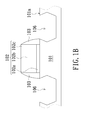
- FIGS. 1A-1E are schematic cross-sectional views illustrating a method for fabricating a metal-oxide-semiconductor field-effect transistor with a compound epitaxial structure according to an embodiment of the present invention
- FIG. 2 is a schematic cross-sectional view illustrating a comparison example of a metal-oxide-semiconductor field-effect transistor
- FIG. 3 is a schematic cross-sectional view illustrating another comparison example of a metal-oxide-semiconductor field-effect transistor
- FIG. 4 illustrates flow rates of the silane gas and the hydrogen chloride gas with respect to the operating time in some other embodiments
- FIG. 5 illustrates flow rates of the silane gas and the hydrogen chloride gas controlled in a stepped increase mode with the deposition time in some embodiments
- FIG. 6 illustrates flow rate of the diborane gas being linearly decreased with respect to the operating time during the process of depositing the liner layer in another embodiment
- FIG. 7 illustrates flow rate of the silane gas being kept constant in the present embodiment.
- the present invention provides a compound semiconductor epitaxial structure and a method for fabricating the compound semiconductor epitaxial structure.
- FIGS. 1A ⁇ 1E are schematic cross-sectional views illustrating the method for fabricating a metal-oxide-semiconductor field-effect transistor 10 with a compound epitaxial structure 100 according to the embodiment of the present invention.
- the method for fabricating the metal-oxide-semiconductor field-effect transistor 10 comprises the following steps. Firstly, as shown in FIG. 1A , a substrate 101 is provided, and a gate structure 102 is formed on a surface 101 a of the substrate 101 .
- the substrate 101 is a silicon wafer.
- the gate structure 102 comprises a gate dielectric layer 102 a and a gate conductor layer 102 b .
- the gate dielectric layer 102 a is formed on the surface 101 a of the substrate 101 .
- the gate conductor layer 102 b is formed on the gate dielectric layer 102 a .
- a spacer 103 is formed on a sidewall of the gate structure 102 .
- a gate cap layer 102 c is formed over the gate conductor layer 102 b.
- a trench structure 106 is formed in the substrate 101 .
- the trench structure 106 is located beside the gate structure 102 .
- the trench structure 106 is formed by performing an isotropic etching process to partially remove the substrate 101 at both sides of the spacer 103 .
- the depth of the trench structure 106 is in the range between 700 nm and 800 nm.
- the trench structure 106 is extended to the region under the space 103 .
- a pre-cleaning process is performed to clean the surface of the substrate 101 at the bottom of the trench structure 106 .
- a silicon germanium epitaxial layer 107 is formed in the trench structure 106 serving as the source/drain regions of the metal-oxide-semiconductor field-effect transistor 10 .
- the silicon germanium epitaxial layer 107 is formed by performing a chemical vapor deposition process.
- a germane gas (GeH 4 ), a dichlorosilane gas (SiH 2 Cl 2 ) and a diborane gas (B 2 H 6 ) is used as a (precursor) reactive gas, and a hydrogen gas (H 2 ), a nitrogen gas (N 2 ) or a hydrogen chloride gas (HCl) is served as a carrier gas. Consequently, a silicon germanium bulk layer containing 40 wt % or more of germanium and 25 wt % of boron dopant is deposited within the trench structure 106 .
- the silicon germanium epitaxial layer 107 is filled in the trench structure 106 and formed over the surface 101 a of the substrate 101 by a height difference H.
- the height difference H between the top surface of the silicon germanium epitaxial layer 107 and the surface 101 a of the substrate 101 is in the range between 150 ⁇ and 170 ⁇ .
- the content of germanium and the concentration of the boron dopant in the silicon germanium epitaxial layer 107 may be controlled by using a mass flow controller (MFC) to adjust the flow rates of the germane gas, the hydrogen chloride gas and the diborane gas.
- MFC mass flow controller
- the concentration and distribution of the boron dopant in the silicon germanium epitaxial layer 107 are correspondingly controlled. Consequently, the silicon germanium epitaxial layer 107 may contain 40 wt % of germanium and a linear gradient concentration of boron dopant varying with thickness thereof or otherwise contain a constant concentration of boron dopant.
- a silane gas (SiH 4 ) or a disilane gas (Si 2 H 6 ) is used as the reactive gas in the above chemical vapor deposition process in order to replace the dichlorosilane gas.
- an undoped silicon germanium layer 108 is formed on an inner surface of the trench structure 106 before the silicon germanium epitaxial layer 107 is formed.
- the arrangement of the undoped silicon germanium layer 108 can inhibit external diffusion of the boron dopant to prevent serious problems due to boron diffusion. Consequently, the electrical punch-through effect and the short channel effect resulting from boron diffusion, which is a serious problem, will be avoided.
- the method of forming the undoped silicon germanium layer 108 is similar to the method of forming the silicon germanium epitaxial layer 107 , except that the diborane gas is not used as the precursor reactive gas in forming the undoped silicon germanium layer 108 .
- the undoped silicon germanium layer 108 contains 25 wt % of germanium.
- a mass flow controller may be used to adjust the flow rates of the germane gas, the silane gas (the dichlorosilane gas or the disilane gas) and the hydrogen chloride gas during the process of forming the undoped silicon germanium layer 108 . That is, the flow rate of the germane gas is linearly increased with the deposition time. Consequently, the undoped silicon germanium layer 108 has a linearly-increased concentration gradient of germanium varying with thickness thereof.
- the mass flow controller is used to control the flow rate of the germane gas to be linearly increased from 0 sccm (initial condition) to 270 sccm within 600 seconds of the operating time.
- the flow rates of the silane gas (dichlorosilane gas or disilane gas) and the hydrogen chloride gas may be also linearly increased with the operating time (see FIG. 4 ) or kept constant from the beginning.
- the flow rates of the silane gas (dichlorosilane gas or disilane gas) and the hydrogen chloride gas are linearly increased from 0 sccm. Consequently, the germanium concentration of the undoped silicon germanium layer 108 is linearly increased from 0 wt % to 40 wt % as the thickness thereof is increased.
- the flow rate of the germane gas may be kept constant for a predetermined interval of time, and the linearly increased-constant flow rate pattern as described may be repeated as needed.
- the germane concentration distribution of the undoped silicon germanium layer 108 can be controlled in a stepped increase mode with the thickness thereof, so as to enhance its stress effect.
- the flow rates of the silane gas (dichlorosilane gas or disilane gas) and the hydrogen chloride gas may be also controlled in a stepped increase mode with the deposition time (see FIG. 5 ).
- the flow rates of the silane gas (dichlorosilane gas or disilane gas) and the hydrogen chloride gas may be kept constant from the beginning.
- the flow rates of the germane gas, the silane gas (dichlorosilane gas or disilane gas) and the hydrogen chloride gas and the time intervals may be adjusted according to the distribution of the germanium concentration predetermined by the operators.
- the process of depositing the undoped silicon germanium layer 108 may be continued by using the germane gas, the silane gas (dichlorosilane gas or disilane gas), the hydrogen chloride gas and the additional diborane gas as the precursor reactive gas to form the silicon germanium epitaxial layer 107 in situ.
- the liner layer 109 has a linearly-decreased concentration gradient of germanium varying with thickness thereof.
- the initial germanium concentration of the linearly-increased concentration gradient of germanium of the liner layer 109 is equal to or smaller than the germanium concentration of the silicon germanium epitaxial layer 107 (i.e. may be smaller than 40 wt %), and preferably is equal to the germanium concentration of the silicon germanium epitaxial layer 107 .
- the initial germanium concentration of the linearly-increased concentration gradient of germanium of the liner layer 109 is 25 wt %.
- the method of forming the liner layer 109 is substantially similar to the method of forming the silicon germanium epitaxial layer 107 , except that the germanium concentration distribution of the liner layer 109 is distinguished.
- the flow rate of the germane gas is linearly decreased with the deposition time.
- a silicon germanium epitaxial liner layer having a thickness of 30 ⁇ 100 ⁇ and a linearly-decreased concentration gradient of germanium varying with thickness of the silicon germanium epitaxial liner layer is formed.
- the flow rate of the germane gas is linearly decreased from 270 sccm (initial) to 0 sccm within 200 seconds of the operating time.
- the flow rates of the hydrogen chloride gas, the diborane gas and the silane gas may be also linearly decreased with the operating time or kept constant from the beginning.
- the flow rates of the hydrogen chloride gas, the diborane gas and the silane gas are linearly decreased along with the decreasing flow rate of the germane gas, such that, the growth rate of the liner layer 109 can be substantially kept constant, and the process can be controlled more easily.
- the flow rate of the diborane gas is linearly decreased from 60 sccm (initial) to 0 sccm within 200 seconds of the operating time (see FIG. 6 ). Consequently, the thickness of the liner layer 109 is substantially 80 ⁇ , and the germanium concentration of the liner layer 109 is linearly decreased from 25 wt % to 0 wt % as the thickness of the liner layer 109 is increased.
- the flow rate of the germane gas may be kept constant for a predetermined interval of time, and the linearly decreased-constant flow rate pattern as described may be repeated.
- the flow rate of the germane gas can be controlled in a stepped decrease mode with the deposition time.
- the flow rates of the diborane gas and the hydrogen chloride gas may be also controlled in a stepped decrease mode with the deposition time.
- the flow rates of the hydrogen chloride gas should be decreased or kept constant simultaneously with the variation of the flow rate of the germane gas.
- the flow rates of the silane gas (dichlorosilane gas or disilane gas) is kept constant from the beginning (see FIG. 7 ).
- the in-situ process indicates that the silicon germanium epitaxial layer 107 and the liner layer 109 are produced in the same reaction chamber or the same processing machine.
- the deposition temperature of forming the liner layer 109 is identical to the deposition temperature of forming the silicon germanium epitaxial layer 107 .
- the undoped silicon germanium layer 108 and the silicon germanium epitaxial layer 107 and the liner layer 109 may be produced in-situ in the same reaction chamber or the same processing machine.
- a cap layer 110 is formed on the liner layer 109 . Meanwhile, the compound semiconductor epitaxial structure 100 of the metal-oxide-semiconductor field-effect transistor 10 is produced.
- the cap layer 110 is formed by depositing a silicon material layer on the liner layer 109 .
- the thickness of the cap layer 110 substantially ranges from 50 ⁇ to 150 ⁇ .
- the process of depositing liner layer 109 may be continued by using the silane gas (dichlorosilane gas or disilane gas), the hydrogen chloride gas and the diborane gas as the precursor reactive gas to form the cap layer 110 in situ.
- the flow rates of the silane gas (dichlorosilane gas or disilane gas), the hydrogen chloride gas and the diborane gas, which continue form the end of the liner layer 109 depositing process, are kept constant to form the cap layer 110 .
- the compressive stress is readily relaxed.
- the liner layer 109 is a single-layered structure whose germanium concentration is linearly decreased with thickness thereof, the problem due to lattice mismatch between adjacent silicon germanium epitaxial liner layers will be eliminated. As a result, the stress relaxation problem of the silicon germanium epitaxial structure will be minimized.
- FIG. 2 is a schematic cross-sectional view illustrating a comparison example of a metal-oxide-semiconductor field-effect transistor 20 .
- FIG. 3 is a schematic cross-sectional view illustrating another comparison example of a metal-oxide-semiconductor field-effect transistor 30 .
- the metal-oxide-semiconductor field-effect transistors 20 and 30 are substantially similar to the metal-oxide-semiconductor field-effect transistor 10 as shown in FIG. 1E , except that the compound semiconductor epitaxial structures 200 and 300 are further distinguished from the compound semiconductor epitaxial structure 100 , in particular with respect to the material composition and concentration thereof, as follow.
- the silicon germanium epitaxial liner layer 109 has a linearly-decreased concentration gradient of germanium varying with thickness thereof.
- the silicon germanium epitaxial liner layer 209 is a single-layered structure having a fixed germanium concentration (e.g. 25 wt %).
- the compound semiconductor epitaxial structure 300 has a first silicon germanium epitaxial liner layer 309 a containing 30 wt % of germanium and a second silicon germanium epitaxial liner layer 309 b containing 8 wt % of germanium.
- identical components of the metal-oxide-semiconductor field-effect transistors 10 , 20 and 30 are designated by identical numeral references.
- the results of the strain and relaxation tests demonstrate that the relaxation percentages for the compound semiconductor epitaxial structures 100 , 200 and 300 are respectively 0.43%, 17.01% and 19.82% relative to the silicon germanium epitaxial structure without the liner layer. It is found that the liner layer 109 whose germanium concentration is linearly decreased with thickness thereof is effective in solving the delamination problem resulting from the lattice mismatch between the compound semiconductor epitaxial structure 100 and other material layers. Moreover, the stress relaxation problem of the silicon germanium epitaxial structure resulted from the multilayered silicon germanium epitaxial liner structure will be minimized.
- the liner layer 109 is produced by dynamically adjusting the concentration of the deposition gas and performing a single continuous epitaxial deposition process, the pre-cleaning and pumping & purging process necessary to be performed during the time period between individual processes of forming the silicon germanium epitaxial liner layers 309 a and 309 b as shown in FIG. 3 may be omitted.
- the method for fabricating the compound semiconductor epitaxial structure 100 according to the present invention is simplified.
- the method of the present invention is able to prevent abrupt temperature changes during the time period between individual processes, so that the thermal shock problem is eliminated.
- the embodiments of present invention provide a compound semiconductor epitaxial structure and a method for fabricating the compound semiconductor epitaxial structure. Firstly, a first compound epitaxial layer is formed in a substrate. Then, by dynamically adjusting the concentration of the deposition gas and performing a single continuous epitaxial deposition process, a second compound epitaxial layer is formed on the first compound epitaxial layer. Consequently, the second compound epitaxial layer has a linearly-decreased concentration gradient of metal. Then, a semiconductor material layer is formed on the second compound epitaxial layer. Since the interfacial lattice mismatch between the compound epitaxial layers is reduced, the stress relaxation problem of the compound epitaxial structure will be minimized and the device performance of the MOSFET will be enhanced.
- the material of forming the compound semiconductor epitaxial structure is not limited to the silicon germanium epitaxial material, and the application of the compound semiconductor epitaxial structure is not limited to the metal-oxide-semiconductor field-effect transistor.
- the compound semiconductor epitaxial structure can be applied by a fin field effect transistor (FINFET).
- FINFET fin field effect transistor
Abstract
Description
Claims (16)
Priority Applications (1)
| Application Number | Priority Date | Filing Date | Title |
|---|---|---|---|
| US13/606,007 US8710632B2 (en) | 2012-09-07 | 2012-09-07 | Compound semiconductor epitaxial structure and method for fabricating the same |
Applications Claiming Priority (1)
| Application Number | Priority Date | Filing Date | Title |
|---|---|---|---|
| US13/606,007 US8710632B2 (en) | 2012-09-07 | 2012-09-07 | Compound semiconductor epitaxial structure and method for fabricating the same |
Publications (2)
| Publication Number | Publication Date |
|---|---|
| US20140070377A1 US20140070377A1 (en) | 2014-03-13 |
| US8710632B2 true US8710632B2 (en) | 2014-04-29 |
Family
ID=50232434
Family Applications (1)
| Application Number | Title | Priority Date | Filing Date |
|---|---|---|---|
| US13/606,007 Active US8710632B2 (en) | 2012-09-07 | 2012-09-07 | Compound semiconductor epitaxial structure and method for fabricating the same |
Country Status (1)
| Country | Link |
|---|---|
| US (1) | US8710632B2 (en) |
Cited By (5)
| Publication number | Priority date | Publication date | Assignee | Title |
|---|---|---|---|---|
| US20150171209A1 (en) * | 2013-04-11 | 2015-06-18 | Boe Technology Group Co., Ltd. | Thin film layer and manufacturing method thereof, substrate for display and liquid crystal display |
| US9214551B2 (en) * | 2014-02-19 | 2015-12-15 | United Microelectronics Corp. | Method for fabricating semiconductor device, and semiconductor device made thereby |
| CN105448991A (en) * | 2014-09-01 | 2016-03-30 | 中芯国际集成电路制造(上海)有限公司 | Transistor and method of forming same |
| US20160254351A1 (en) * | 2015-02-26 | 2016-09-01 | Taiwan Semiconductor Manufacturing Company Ltd. | Ldd-free semiconductor structure and manufacturing method of the same |
| US20180166572A1 (en) * | 2014-07-10 | 2018-06-14 | Taiwan Semiconductor Manufacturing Company Ltd. | Method for manufacturing semiconductor structure |
Families Citing this family (18)
| Publication number | Priority date | Publication date | Assignee | Title |
|---|---|---|---|---|
| US8994104B2 (en) * | 1999-09-28 | 2015-03-31 | Intel Corporation | Contact resistance reduction employing germanium overlayer pre-contact metalization |
| US9484432B2 (en) | 2010-12-21 | 2016-11-01 | Intel Corporation | Contact resistance reduction employing germanium overlayer pre-contact metalization |
| US8901537B2 (en) | 2010-12-21 | 2014-12-02 | Intel Corporation | Transistors with high concentration of boron doped germanium |
| US8963258B2 (en) * | 2013-03-13 | 2015-02-24 | Taiwan Semiconductor Manufacturing Company | FinFET with bottom SiGe layer in source/drain |
| US9691898B2 (en) * | 2013-12-19 | 2017-06-27 | Taiwan Semiconductor Manufacturing Co., Ltd. | Germanium profile for channel strain |
| US9287398B2 (en) | 2014-02-14 | 2016-03-15 | Taiwan Semiconductor Manufacturing Co., Ltd. | Transistor strain-inducing scheme |
| US9276113B2 (en) * | 2014-03-10 | 2016-03-01 | International Business Corporation | Structure and method to make strained FinFET with improved junction capacitance and low leakage |
| KR102167519B1 (en) | 2014-03-21 | 2020-10-19 | 인텔 코포레이션 | Techniques for integration of ge-rich p-mos source/drain contacts |
| CN105280496B (en) * | 2014-06-05 | 2019-06-11 | 联华电子股份有限公司 | Semiconductor element and preparation method thereof with fin structure |
| US9269777B2 (en) * | 2014-07-23 | 2016-02-23 | Taiwan Semiconductor Manufacturing Company, Ltd. | Source/drain structures and methods of forming same |
| CN105405881B (en) * | 2014-08-20 | 2020-07-07 | 中国科学院微电子研究所 | Semiconductor device and method for manufacturing the same |
| CN105632927B (en) * | 2014-10-30 | 2018-09-07 | 中芯国际集成电路制造(上海)有限公司 | The forming method of PMOS transistor |
| EP3394896A4 (en) | 2015-12-24 | 2019-12-18 | Intel Corporation | Methods of forming doped source/drain contacts and structures formed thereby |
| US10141426B2 (en) * | 2016-02-08 | 2018-11-27 | International Business Macahines Corporation | Vertical transistor device |
| CN107369644B (en) * | 2016-05-12 | 2021-11-02 | 联华电子股份有限公司 | Semiconductor element and manufacturing method thereof |
| CN107403835B (en) * | 2016-05-19 | 2021-12-14 | 联芯集成电路制造(厦门)有限公司 | Semiconductor device and manufacturing process thereof |
| KR102403737B1 (en) * | 2018-05-23 | 2022-05-31 | 삼성전자주식회사 | Integrated circuit devices and method for manufacturing the same |
| US11081584B2 (en) * | 2018-10-30 | 2021-08-03 | Taiwan Semiconductor Manufacturing Co., Ltd. | Method of manufacturing semiconductor devices using a capping layer in forming gate electrode and semiconductor devices |
Citations (133)
| Publication number | Priority date | Publication date | Assignee | Title |
|---|---|---|---|---|
| US4891303A (en) | 1988-05-26 | 1990-01-02 | Texas Instruments Incorporated | Trilayer microlithographic process using a silicon-based resist as the middle layer |
| US5217910A (en) | 1990-11-05 | 1993-06-08 | Mitsubishi Denki Kabushiki Kaisha | Method of fabricating semiconductor device having sidewall spacers and oblique implantation |
| US5273930A (en) | 1992-09-03 | 1993-12-28 | Motorola, Inc. | Method of forming a non-selective silicon-germanium epitaxial film |
| US5356830A (en) | 1988-09-19 | 1994-10-18 | Kabushiki Kaisha Tobshiba | Semiconductor device and its manufacturing method |
| US5372957A (en) | 1993-07-22 | 1994-12-13 | Taiwan Semiconductor Manufacturing Company | Multiple tilted angle ion implantation MOSFET method |
| US5385630A (en) | 1993-06-29 | 1995-01-31 | Digital Equipment Corporation | Process for increasing sacrificial oxide etch rate to reduce field oxide loss |
| US5399506A (en) | 1992-08-13 | 1995-03-21 | Sony Corporation | Semiconductor fabricating process |
| US5625217A (en) | 1992-12-11 | 1997-04-29 | Intel Corporation | MOS transistor having a composite gate electrode and method of fabrication |
| US5777364A (en) | 1992-11-30 | 1998-07-07 | International Business Machines Corporation | Graded channel field effect transistor |
| US5783479A (en) | 1997-06-23 | 1998-07-21 | National Science Council | Structure and method for manufacturing improved FETs having T-shaped gates |
| US5960322A (en) | 1997-12-19 | 1999-09-28 | Advanced Micro Devices, Inc. | Suppression of boron segregation for shallow source and drain junctions in semiconductors |
| US6030874A (en) | 1997-01-21 | 2000-02-29 | Texas Instruments Incorporated | Doped polysilicon to retard boron diffusion into and through thin gate dielectrics |
| US6048756A (en) | 1997-07-31 | 2000-04-11 | Electronics And Telecommunications Research Institute | Method for making a silicon-on-insulator MOS transistor using a selective SiGe epitaxy |
| US6074954A (en) | 1998-08-31 | 2000-06-13 | Applied Materials, Inc | Process for control of the shape of the etch front in the etching of polysilicon |
| US6100171A (en) | 1998-03-03 | 2000-08-08 | Advanced Micro Devices, Inc. | Reduction of boron penetration by laser anneal removal of fluorine |
| US6110787A (en) | 1999-09-07 | 2000-08-29 | Chartered Semiconductor Manufacturing Ltd. | Method for fabricating a MOS device |
| US6165826A (en) | 1994-12-23 | 2000-12-26 | Intel Corporation | Transistor with low resistance tip and method of fabrication in a CMOS process |
| US6165881A (en) | 1998-10-23 | 2000-12-26 | Taiwan Semiconductor Manufacturing Company | Method of forming salicide poly gate with thin gate oxide and ultra narrow gate width |
| US6191052B1 (en) | 1999-01-25 | 2001-02-20 | Taiwan Semiconductor Manufacturing Company | Method for fabricating an ultra-shallow junction with low resistance using a screen oxide formed by poly re-oxidation in a nitrogen containing atmosphere |
| US6228730B1 (en) | 1999-04-28 | 2001-05-08 | United Microelectronics Corp. | Method of fabricating field effect transistor |
| US6274447B1 (en) | 1996-03-22 | 2001-08-14 | Seiko Epson Corporation | Semiconductor device comprising a MOS element and a fabrication method thereof |
| US6274894B1 (en) * | 1999-08-17 | 2001-08-14 | Advanced Micro Devices, Inc. | Low-bandgap source and drain formation for short-channel MOS transistors |
| US6355533B2 (en) | 1999-12-24 | 2002-03-12 | Hyundai Electronics Industries Co., Ltd. | Method for manufacturing semiconductor device |
| US6365476B1 (en) | 2000-10-27 | 2002-04-02 | Ultratech Stepper, Inc. | Laser thermal process for fabricating field-effect transistors |
| US6368926B1 (en) | 2000-03-13 | 2002-04-09 | Advanced Micro Devices, Inc. | Method of forming a semiconductor device with source/drain regions having a deep vertical junction |
| US6444591B1 (en) | 2000-09-30 | 2002-09-03 | Newport Fab, Llc | Method for reducing contamination prior to epitaxial growth and related structure |
| US20020160587A1 (en) | 2001-04-30 | 2002-10-31 | Basanth Jagannathan | Method to increase carbon and boron doping concentrations in Si and SiGe films |
| US20020182423A1 (en) | 2001-04-20 | 2002-12-05 | International Business Machines Corporation | Epitaxial and polycrystalline growth of Si1-x-yGexCy and Si1-yCy alloy layers on Si by UHV-CVD |
| US6537370B1 (en) | 1998-09-10 | 2003-03-25 | FRANCE TéLéCOM | Process for obtaining a layer of single-crystal germanium on a substrate of single-crystal silicon, and products obtained |
| US6544822B2 (en) | 2000-06-21 | 2003-04-08 | Hynix Semiconductor, Inc. | Method for fabricating MOSFET device |
| US6605498B1 (en) | 2002-03-29 | 2003-08-12 | Intel Corporation | Semiconductor transistor having a backfilled channel material |
| US6613695B2 (en) | 2000-11-24 | 2003-09-02 | Asm America, Inc. | Surface preparation prior to deposition |
| US6621131B2 (en) | 2001-11-01 | 2003-09-16 | Intel Corporation | Semiconductor transistor having a stressed channel |
| US6624068B2 (en) | 2001-08-24 | 2003-09-23 | Texas Instruments Incorporated | Polysilicon processing using an anti-reflective dual layer hardmask for 193 nm lithography |
| US20030181005A1 (en) | 2002-03-19 | 2003-09-25 | Kiyota Hachimine | Semiconductor device and a method of manufacturing the same |
| US6632718B1 (en) | 1998-07-15 | 2003-10-14 | Texas Instruments Incorporated | Disposable spacer technology for reduced cost CMOS processing |
| US20030203599A1 (en) | 2000-03-27 | 2003-10-30 | Matsushita Electric Industrial Co. , Ltd. | Semiconductor wafer and method for fabricating the same |
| US6642122B1 (en) | 2002-09-26 | 2003-11-04 | Advanced Micro Devices, Inc. | Dual laser anneal for graded halo profile |
| US6664156B1 (en) | 2002-07-31 | 2003-12-16 | Chartered Semiconductor Manufacturing, Ltd | Method for forming L-shaped spacers with precise width control |
| US6676764B2 (en) | 2001-04-30 | 2004-01-13 | Hynix Semiconductor Inc. | Method for cleaning a substrate in selective epitaxial growth process |
| US6703271B2 (en) | 2001-11-30 | 2004-03-09 | Taiwan Semiconductor Manufacturing Company | Complementary metal oxide semiconductor transistor technology using selective epitaxy of a strained silicon germanium layer |
| US20040045499A1 (en) | 2002-06-10 | 2004-03-11 | Amberwave Systems Corporation | Source and drain elements |
| US20040067631A1 (en) | 2002-10-03 | 2004-04-08 | Haowen Bu | Reduction of seed layer roughness for use in forming SiGe gate electrode |
| US6777275B1 (en) | 2000-11-15 | 2004-08-17 | Advanced Micro Devices, Inc. | Single anneal for dopant activation and silicide formation |
| US6806151B2 (en) | 2001-12-14 | 2004-10-19 | Texas Instruments Incorporated | Methods and apparatus for inducing stress in a semiconductor device |
| US6809402B1 (en) | 2002-08-14 | 2004-10-26 | Advanced Micro Devices, Inc. | Reflowable-doped HDP film |
| US20040227164A1 (en) | 2003-05-14 | 2004-11-18 | Samsung Electronics Co., Ltd. | MOS transistor with elevated source/drain structure and method of fabricating the same |
| US6858506B2 (en) | 2002-08-08 | 2005-02-22 | Macronix International Co., Ltd. | Method for fabricating locally strained channel |
| US6864135B2 (en) | 2002-10-31 | 2005-03-08 | Freescale Semiconductor, Inc. | Semiconductor fabrication process using transistor spacers of differing widths |
| US6869867B2 (en) | 1997-10-01 | 2005-03-22 | Kabushiki Kaisha Toshiba | Semiconductor device comprising metal silicide films formed to cover gate electrode and source-drain diffusion layers and method of manufacturing the same wherein the silicide on gate is thicker than on source-drain |
| US20050070076A1 (en) | 2001-10-26 | 2005-03-31 | Dion Michel Maurice | Method of depositing high-quality sige on sige substrates |
| US20050079692A1 (en) | 2003-10-10 | 2005-04-14 | Applied Materials, Inc. | Methods to fabricate MOSFET devices using selective deposition process |
| US20050082616A1 (en) | 2003-10-20 | 2005-04-21 | Huajie Chen | High performance stress-enhanced MOSFETs using Si:C and SiGe epitaxial source/drain and method of manufacture |
| US6887762B1 (en) | 1998-11-12 | 2005-05-03 | Intel Corporation | Method of fabricating a field effect transistor structure with abrupt source/drain junctions |
| US6887751B2 (en) | 2003-09-12 | 2005-05-03 | International Business Machines Corporation | MOSFET performance improvement using deformation in SOI structure |
| US6891192B2 (en) | 2003-08-04 | 2005-05-10 | International Business Machines Corporation | Structure and method of making strained semiconductor CMOS transistors having lattice-mismatched semiconductor regions underlying source and drain regions |
| US20050139231A1 (en) | 2003-12-31 | 2005-06-30 | Commissariat A L'energie Atomique | Method of wet cleaning a surface, especially of a material of the silicon-germanium type |
| US6930007B2 (en) | 2003-09-15 | 2005-08-16 | Texas Instruments Incorporated | Integration of pre-S/D anneal selective nitride/oxide composite cap for improving transistor performance |
| US6946350B2 (en) | 2003-12-31 | 2005-09-20 | Intel Corporation | Controlled faceting of source/drain regions |
| US6962856B2 (en) | 2002-07-19 | 2005-11-08 | Hynix Semiconductor, Inc. | Method for forming device isolation film of semiconductor device |
| US20050260830A1 (en) | 2004-03-25 | 2005-11-24 | Doo-Won Kwon | Methods of fabricating a semiconductor device using a dilute aqueous solution of an ammonia and peroxide mixture |
| US6972461B1 (en) | 2004-06-30 | 2005-12-06 | International Business Machines Corporation | Channel MOSFET with strained silicon channel on strained SiGe |
| US20050285193A1 (en) | 2004-06-28 | 2005-12-29 | Lee Sung-Young | Semiconductor device and method of manufacturing same |
| US20050287752A1 (en) | 2004-06-24 | 2005-12-29 | Applied Materials, Inc. | Methods for forming a transistor |
| US6991979B2 (en) | 2003-09-22 | 2006-01-31 | International Business Machines Corporation | Method for avoiding oxide undercut during pre-silicide clean for thin spacer FETs |
| US6991991B2 (en) | 2003-11-12 | 2006-01-31 | United Microelectronics Corp. | Method for preventing to form a spacer undercut in SEG pre-clean process |
| US20060051922A1 (en) | 2004-09-09 | 2006-03-09 | Taiwan Semiconductor Manufacturing Company, Ltd. | Strained silicon device manufacturing method |
| US20060057859A1 (en) | 2004-09-16 | 2006-03-16 | International Business Machines Corporation | Buffer layer for selective SiGe growth for uniform nucleation |
| US20060076627A1 (en) | 2004-10-12 | 2006-04-13 | International Business Machines Corporation | Ultra shallow junction formation by epitaxial interface limited diffusion |
| US20060088968A1 (en) | 2004-06-17 | 2006-04-27 | Samsung Electronics Co., Ltd. | Methods of fabricating a semiconductor device using a selective epitaxial growth technique |
| US7037773B2 (en) | 2004-03-29 | 2006-05-02 | United Microelectronics Corp. | Method of manufacturing metal-oxide-semiconductor transistor |
| US20060115949A1 (en) | 2004-12-01 | 2006-06-01 | Freescale Semiconductor, Inc. | Semiconductor fabrication process including source/drain recessing and filling |
| US7060579B2 (en) | 2004-07-29 | 2006-06-13 | Texas Instruments Incorporated | Increased drive current by isotropic recess etch |
| US7060576B2 (en) | 2003-10-24 | 2006-06-13 | Intel Corporation | Epitaxially deposited source/drain |
| US7112495B2 (en) | 2003-08-15 | 2006-09-26 | Taiwan Semiconductor Manufacturing Company, Ltd. | Structure and method of a strained channel transistor and a second semiconductor component in an integrated circuit |
| US7118952B2 (en) | 2004-07-14 | 2006-10-10 | Taiwan Semiconductor Manufacturing Co., Ltd. | Method of making transistor with strained source/drain |
| US20060228842A1 (en) | 2005-04-07 | 2006-10-12 | Freescale Semiconductor, Inc. | Transistor fabrication using double etch/refill process |
| US20060231826A1 (en) | 2005-04-18 | 2006-10-19 | Toshiba America Electronic Components, Inc. | Step-embedded SiGe structure for PFET mobility enhancement |
| US20060258126A1 (en) | 2003-02-04 | 2006-11-16 | Sumco Corporation | Semiconductor substrate, field-effect transistor, and their production methods |
| US20060281288A1 (en) | 2005-06-13 | 2006-12-14 | Fujitsu Limited | Semiconductor device fabrication method |
| US20060292779A1 (en) | 2004-09-29 | 2006-12-28 | International Business Machines Corporation | Structure and method for making strained channel field effect transistor using sacrificial spacer |
| US20060292783A1 (en) | 2005-02-28 | 2006-12-28 | Young-Eun Lee | CMOS transistor and method of manufacturing the same |
| US7169675B2 (en) | 2004-07-07 | 2007-01-30 | Chartered Semiconductor Manufacturing, Ltd | Material architecture for the fabrication of low temperature transistor |
| US20070023847A1 (en) | 2005-07-26 | 2007-02-01 | Samsung Electronics Co., Ltd. | Semiconductor device and method of manufacturing the same |
| US20070034906A1 (en) | 2005-08-10 | 2007-02-15 | Taiwan Semiconductor Manufacturing Company, Ltd. | MOS devices with reduced recess on substrate surface |
| US7183596B2 (en) | 2005-06-22 | 2007-02-27 | Taiwan Semiconductor Manufacturing Company, Ltd. | Composite gate structure in an integrated circuit |
| US20070049014A1 (en) | 2005-08-25 | 2007-03-01 | Ming-Tsung Chen | Method of performing salicide processes on MOS transistors |
| US20070072376A1 (en) | 2005-09-29 | 2007-03-29 | Semiconductor Manufacturing International (Shanghai) Corporation | Strained-induced mobility enhancement nano-device structure and integrated process architecture for CMOS technologies |
| US20070072353A1 (en) | 2005-09-23 | 2007-03-29 | Chih-Ning Wu | Method of fabricating strained-silicon transistors and strained-silicon CMOS transistors |
| US7202124B2 (en) | 2004-10-01 | 2007-04-10 | Massachusetts Institute Of Technology | Strained gettering layers for semiconductor processes |
| US7217627B2 (en) | 2003-09-18 | 2007-05-15 | Dongbu Electronics Co., Ltd. | Semiconductor devices having diffusion barrier regions and halo implant regions and methods of fabricating the same |
| US20070128783A1 (en) | 2005-12-06 | 2007-06-07 | Shyh-Fann Ting | Method for fabricating strained-silicon cmos transistors |
| US20070166929A1 (en) | 2006-01-18 | 2007-07-19 | Sumco Corporation | Method of producing semiconductor wafer |
| US7288822B1 (en) | 2006-04-07 | 2007-10-30 | United Microelectronics Corp. | Semiconductor structure and fabricating method thereof |
| US20070262396A1 (en) | 2006-04-25 | 2007-11-15 | International Business Machines Corporation | Transistors Having V-shape Source/Drain Metal Contacts |
| US7303999B1 (en) | 2005-12-13 | 2007-12-04 | Lam Research Corporation | Multi-step method for etching strain gate recesses |
| US20080014688A1 (en) | 2006-07-06 | 2008-01-17 | Voon-Yew Thean | Selective uniaxial stress modification for use with strained silicon on insulator integrated circuit |
| US7335959B2 (en) | 2005-01-06 | 2008-02-26 | Intel Corporation | Device with stepped source/drain region profile |
| US20080061366A1 (en) | 2006-09-11 | 2008-03-13 | United Microelectronics Corp. | Complementary metal-oxide-semiconductor device and fabricating method thereof |
| US20080067545A1 (en) | 2006-09-20 | 2008-03-20 | Samsung Electronics Co., Ltd | Semiconductor device including field effect transistor and method of forming the same |
| US20080076236A1 (en) | 2006-09-21 | 2008-03-27 | Jih-Shun Chiang | Method for forming silicon-germanium epitaxial layer |
| US20080085577A1 (en) | 2006-10-05 | 2008-04-10 | Hung-Lin Shih | Method of manufacturing complementary metal oxide semiconductor transistor |
| US20080116525A1 (en) | 2006-11-16 | 2008-05-22 | United Microelectronics Corp. | Complementary metal-oxide-semiconductor device |
| US20080124874A1 (en) | 2006-11-03 | 2008-05-29 | Samsung Electronics Co., Ltd. | Methods of Forming Field Effect Transistors Having Silicon-Germanium Source and Drain Regions |
| US20080128746A1 (en) | 2006-12-05 | 2008-06-05 | Yin-Pin Wang | Dual-SiGe epitaxy for MOS devices |
| US20080128765A1 (en) * | 2004-12-15 | 2008-06-05 | Chien-Hao Chen | MOSFET Device With Localized Stressor |
| US20080142886A1 (en) | 2006-12-18 | 2008-06-19 | Chin-I Liao | Treatment method of semiconductor, method for manufacturing mos, and mos structure |
| US20080157119A1 (en) * | 2006-12-29 | 2008-07-03 | Pang-Yen Tsai | Stack SiGe for short channel improvement |
| US7410859B1 (en) | 2005-11-07 | 2008-08-12 | Advanced Micro Devices, Inc. | Stressed MOS device and method for its fabrication |
| US20080220579A1 (en) | 2007-03-07 | 2008-09-11 | Advanced Micro Devices, Inc. | Stress enhanced mos transistor and methods for its fabrication |
| US20080233746A1 (en) | 2007-03-21 | 2008-09-25 | Hui-Ling Huang | Method for manufacturing mos transistors utilizing a hybrid hard mask |
| US20080233722A1 (en) | 2007-03-23 | 2008-09-25 | United Microelectronics Corp. | Method of forming selective area compound semiconductor epitaxial layer |
| US7462239B2 (en) | 2001-05-30 | 2008-12-09 | Asm America, Inc. | Low temperature load and bake |
| US20090039389A1 (en) | 2007-08-09 | 2009-02-12 | Chu-Yin Tseng | Method of fabricating metal oxide semiconductor transistor |
| US20090045456A1 (en) | 2007-08-13 | 2009-02-19 | United Microelectronics Corp. | Semiconductor device and method of fabricating the same |
| US7494858B2 (en) | 2005-06-30 | 2009-02-24 | Intel Corporation | Transistor with improved tip profile and method of manufacture thereof |
| US7494856B2 (en) | 2006-03-30 | 2009-02-24 | Freescale Semiconductor, Inc. | Semiconductor fabrication process using etch stop layer to optimize formation of source/drain stressor |
| US20090095992A1 (en) | 2006-12-22 | 2009-04-16 | Tomoya Sanuki | Semiconductor device including mos field effect transistor and method for manufacturing the semiconductor device |
| US20090117715A1 (en) | 2006-02-27 | 2009-05-07 | Fujitsu Limited | Semiconductor device fabricated by selective epitaxial growth method |
| US20090124056A1 (en) | 2007-11-12 | 2009-05-14 | United Microelectronics Corp. | Method of fabricating semiconductor device |
| US20090166625A1 (en) | 2007-12-28 | 2009-07-02 | United Microelectronics Corp. | Mos device structure |
| US20090184402A1 (en) | 2008-01-22 | 2009-07-23 | United Microelectronics Corp. | Method of fabricating a shallow trench isolation structure including forming a second liner covering the corner of the trench and first liner. |
| US20090186475A1 (en) | 2008-01-21 | 2009-07-23 | Shyh-Fann Ting | Method of manufacturing a MOS transistor |
| US7592231B2 (en) | 2006-08-01 | 2009-09-22 | United Microelectronics Corp. | MOS transistor and fabrication thereof |
| US20090246922A1 (en) | 2008-03-27 | 2009-10-01 | Meng-Yi Wu | Method of forming cmos transistor |
| US20090278170A1 (en) | 2008-05-07 | 2009-11-12 | Yun-Chi Yang | Semiconductor device and manufacturing method thereof |
| US20090302348A1 (en) | 2008-06-10 | 2009-12-10 | International Business Machines Corporation | Stress enhanced transistor devices and methods of making |
| US20100001317A1 (en) | 2008-07-03 | 2010-01-07 | Yi-Wei Chen | Cmos transistor and the method for manufacturing the same |
| US7667227B2 (en) | 2004-12-28 | 2010-02-23 | Fujitsu Microelectronics Limited | Semiconductor device and fabrication method thereof |
| US7691752B2 (en) | 2007-03-30 | 2010-04-06 | Intel Corporation | Methods of forming improved EPI fill on narrow isolation bounded source/drain regions and structures formed thereby |
| US20100093147A1 (en) | 2008-10-14 | 2010-04-15 | Chin-I Liao | Method for forming a semiconductor device |
| US7838370B2 (en) | 2006-12-27 | 2010-11-23 | Texas Instruments Incorporated | Highly selective liners for semiconductor fabrication |
| US20110254105A1 (en) * | 2010-04-16 | 2011-10-20 | Taiwan Semiconductor Manufacturing Company. Ltd. | Strained Semiconductor Device with Recessed Channel |
-
2012
- 2012-09-07 US US13/606,007 patent/US8710632B2/en active Active
Patent Citations (140)
| Publication number | Priority date | Publication date | Assignee | Title |
|---|---|---|---|---|
| US4891303A (en) | 1988-05-26 | 1990-01-02 | Texas Instruments Incorporated | Trilayer microlithographic process using a silicon-based resist as the middle layer |
| US5356830A (en) | 1988-09-19 | 1994-10-18 | Kabushiki Kaisha Tobshiba | Semiconductor device and its manufacturing method |
| US5217910A (en) | 1990-11-05 | 1993-06-08 | Mitsubishi Denki Kabushiki Kaisha | Method of fabricating semiconductor device having sidewall spacers and oblique implantation |
| US5399506A (en) | 1992-08-13 | 1995-03-21 | Sony Corporation | Semiconductor fabricating process |
| US5273930A (en) | 1992-09-03 | 1993-12-28 | Motorola, Inc. | Method of forming a non-selective silicon-germanium epitaxial film |
| US5777364A (en) | 1992-11-30 | 1998-07-07 | International Business Machines Corporation | Graded channel field effect transistor |
| US5625217A (en) | 1992-12-11 | 1997-04-29 | Intel Corporation | MOS transistor having a composite gate electrode and method of fabrication |
| US5783478A (en) | 1992-12-11 | 1998-07-21 | Intel Corporation | Method of frabricating a MOS transistor having a composite gate electrode |
| US5385630A (en) | 1993-06-29 | 1995-01-31 | Digital Equipment Corporation | Process for increasing sacrificial oxide etch rate to reduce field oxide loss |
| US5372957A (en) | 1993-07-22 | 1994-12-13 | Taiwan Semiconductor Manufacturing Company | Multiple tilted angle ion implantation MOSFET method |
| US6165826A (en) | 1994-12-23 | 2000-12-26 | Intel Corporation | Transistor with low resistance tip and method of fabrication in a CMOS process |
| US6274447B1 (en) | 1996-03-22 | 2001-08-14 | Seiko Epson Corporation | Semiconductor device comprising a MOS element and a fabrication method thereof |
| US6030874A (en) | 1997-01-21 | 2000-02-29 | Texas Instruments Incorporated | Doped polysilicon to retard boron diffusion into and through thin gate dielectrics |
| US5783479A (en) | 1997-06-23 | 1998-07-21 | National Science Council | Structure and method for manufacturing improved FETs having T-shaped gates |
| US6048756A (en) | 1997-07-31 | 2000-04-11 | Electronics And Telecommunications Research Institute | Method for making a silicon-on-insulator MOS transistor using a selective SiGe epitaxy |
| US6869867B2 (en) | 1997-10-01 | 2005-03-22 | Kabushiki Kaisha Toshiba | Semiconductor device comprising metal silicide films formed to cover gate electrode and source-drain diffusion layers and method of manufacturing the same wherein the silicide on gate is thicker than on source-drain |
| US5960322A (en) | 1997-12-19 | 1999-09-28 | Advanced Micro Devices, Inc. | Suppression of boron segregation for shallow source and drain junctions in semiconductors |
| US6100171A (en) | 1998-03-03 | 2000-08-08 | Advanced Micro Devices, Inc. | Reduction of boron penetration by laser anneal removal of fluorine |
| US6632718B1 (en) | 1998-07-15 | 2003-10-14 | Texas Instruments Incorporated | Disposable spacer technology for reduced cost CMOS processing |
| US6699763B2 (en) | 1998-07-15 | 2004-03-02 | Texas Instruments Incorporated | Disposable spacer technology for reduced cost CMOS processing |
| US6074954A (en) | 1998-08-31 | 2000-06-13 | Applied Materials, Inc | Process for control of the shape of the etch front in the etching of polysilicon |
| US6537370B1 (en) | 1998-09-10 | 2003-03-25 | FRANCE TéLéCOM | Process for obtaining a layer of single-crystal germanium on a substrate of single-crystal silicon, and products obtained |
| US6165881A (en) | 1998-10-23 | 2000-12-26 | Taiwan Semiconductor Manufacturing Company | Method of forming salicide poly gate with thin gate oxide and ultra narrow gate width |
| US6887762B1 (en) | 1998-11-12 | 2005-05-03 | Intel Corporation | Method of fabricating a field effect transistor structure with abrupt source/drain junctions |
| US6191052B1 (en) | 1999-01-25 | 2001-02-20 | Taiwan Semiconductor Manufacturing Company | Method for fabricating an ultra-shallow junction with low resistance using a screen oxide formed by poly re-oxidation in a nitrogen containing atmosphere |
| US6228730B1 (en) | 1999-04-28 | 2001-05-08 | United Microelectronics Corp. | Method of fabricating field effect transistor |
| US6274894B1 (en) * | 1999-08-17 | 2001-08-14 | Advanced Micro Devices, Inc. | Low-bandgap source and drain formation for short-channel MOS transistors |
| US6110787A (en) | 1999-09-07 | 2000-08-29 | Chartered Semiconductor Manufacturing Ltd. | Method for fabricating a MOS device |
| US6355533B2 (en) | 1999-12-24 | 2002-03-12 | Hyundai Electronics Industries Co., Ltd. | Method for manufacturing semiconductor device |
| US6368926B1 (en) | 2000-03-13 | 2002-04-09 | Advanced Micro Devices, Inc. | Method of forming a semiconductor device with source/drain regions having a deep vertical junction |
| US20030203599A1 (en) | 2000-03-27 | 2003-10-30 | Matsushita Electric Industrial Co. , Ltd. | Semiconductor wafer and method for fabricating the same |
| US6544822B2 (en) | 2000-06-21 | 2003-04-08 | Hynix Semiconductor, Inc. | Method for fabricating MOSFET device |
| US6444591B1 (en) | 2000-09-30 | 2002-09-03 | Newport Fab, Llc | Method for reducing contamination prior to epitaxial growth and related structure |
| US6365476B1 (en) | 2000-10-27 | 2002-04-02 | Ultratech Stepper, Inc. | Laser thermal process for fabricating field-effect transistors |
| US6777275B1 (en) | 2000-11-15 | 2004-08-17 | Advanced Micro Devices, Inc. | Single anneal for dopant activation and silicide formation |
| US6613695B2 (en) | 2000-11-24 | 2003-09-02 | Asm America, Inc. | Surface preparation prior to deposition |
| US20020182423A1 (en) | 2001-04-20 | 2002-12-05 | International Business Machines Corporation | Epitaxial and polycrystalline growth of Si1-x-yGexCy and Si1-yCy alloy layers on Si by UHV-CVD |
| US6676764B2 (en) | 2001-04-30 | 2004-01-13 | Hynix Semiconductor Inc. | Method for cleaning a substrate in selective epitaxial growth process |
| US20020160587A1 (en) | 2001-04-30 | 2002-10-31 | Basanth Jagannathan | Method to increase carbon and boron doping concentrations in Si and SiGe films |
| US7462239B2 (en) | 2001-05-30 | 2008-12-09 | Asm America, Inc. | Low temperature load and bake |
| US6624068B2 (en) | 2001-08-24 | 2003-09-23 | Texas Instruments Incorporated | Polysilicon processing using an anti-reflective dual layer hardmask for 193 nm lithography |
| US20050070076A1 (en) | 2001-10-26 | 2005-03-31 | Dion Michel Maurice | Method of depositing high-quality sige on sige substrates |
| US6861318B2 (en) | 2001-11-01 | 2005-03-01 | Intel Corporation | Semiconductor transistor having a stressed channel |
| US6621131B2 (en) | 2001-11-01 | 2003-09-16 | Intel Corporation | Semiconductor transistor having a stressed channel |
| US6703271B2 (en) | 2001-11-30 | 2004-03-09 | Taiwan Semiconductor Manufacturing Company | Complementary metal oxide semiconductor transistor technology using selective epitaxy of a strained silicon germanium layer |
| US6806151B2 (en) | 2001-12-14 | 2004-10-19 | Texas Instruments Incorporated | Methods and apparatus for inducing stress in a semiconductor device |
| US20030181005A1 (en) | 2002-03-19 | 2003-09-25 | Kiyota Hachimine | Semiconductor device and a method of manufacturing the same |
| US6605498B1 (en) | 2002-03-29 | 2003-08-12 | Intel Corporation | Semiconductor transistor having a backfilled channel material |
| US20040045499A1 (en) | 2002-06-10 | 2004-03-11 | Amberwave Systems Corporation | Source and drain elements |
| US6962856B2 (en) | 2002-07-19 | 2005-11-08 | Hynix Semiconductor, Inc. | Method for forming device isolation film of semiconductor device |
| US6664156B1 (en) | 2002-07-31 | 2003-12-16 | Chartered Semiconductor Manufacturing, Ltd | Method for forming L-shaped spacers with precise width control |
| US6858506B2 (en) | 2002-08-08 | 2005-02-22 | Macronix International Co., Ltd. | Method for fabricating locally strained channel |
| US6809402B1 (en) | 2002-08-14 | 2004-10-26 | Advanced Micro Devices, Inc. | Reflowable-doped HDP film |
| US6642122B1 (en) | 2002-09-26 | 2003-11-04 | Advanced Micro Devices, Inc. | Dual laser anneal for graded halo profile |
| US20040067631A1 (en) | 2002-10-03 | 2004-04-08 | Haowen Bu | Reduction of seed layer roughness for use in forming SiGe gate electrode |
| US6864135B2 (en) | 2002-10-31 | 2005-03-08 | Freescale Semiconductor, Inc. | Semiconductor fabrication process using transistor spacers of differing widths |
| US20060258126A1 (en) | 2003-02-04 | 2006-11-16 | Sumco Corporation | Semiconductor substrate, field-effect transistor, and their production methods |
| US20040227164A1 (en) | 2003-05-14 | 2004-11-18 | Samsung Electronics Co., Ltd. | MOS transistor with elevated source/drain structure and method of fabricating the same |
| US20060163558A1 (en) | 2003-05-14 | 2006-07-27 | Samsung Electronics, Co., Ltd. | MOS transistor with elevated source/drain structure |
| US6891192B2 (en) | 2003-08-04 | 2005-05-10 | International Business Machines Corporation | Structure and method of making strained semiconductor CMOS transistors having lattice-mismatched semiconductor regions underlying source and drain regions |
| US7112495B2 (en) | 2003-08-15 | 2006-09-26 | Taiwan Semiconductor Manufacturing Company, Ltd. | Structure and method of a strained channel transistor and a second semiconductor component in an integrated circuit |
| US6887751B2 (en) | 2003-09-12 | 2005-05-03 | International Business Machines Corporation | MOSFET performance improvement using deformation in SOI structure |
| US6930007B2 (en) | 2003-09-15 | 2005-08-16 | Texas Instruments Incorporated | Integration of pre-S/D anneal selective nitride/oxide composite cap for improving transistor performance |
| US7217627B2 (en) | 2003-09-18 | 2007-05-15 | Dongbu Electronics Co., Ltd. | Semiconductor devices having diffusion barrier regions and halo implant regions and methods of fabricating the same |
| US6991979B2 (en) | 2003-09-22 | 2006-01-31 | International Business Machines Corporation | Method for avoiding oxide undercut during pre-silicide clean for thin spacer FETs |
| US7132338B2 (en) | 2003-10-10 | 2006-11-07 | Applied Materials, Inc. | Methods to fabricate MOSFET devices using selective deposition process |
| US20070082451A1 (en) | 2003-10-10 | 2007-04-12 | Samoilov Arkadii V | Methods to fabricate mosfet devices using a selective deposition process |
| US20050079692A1 (en) | 2003-10-10 | 2005-04-14 | Applied Materials, Inc. | Methods to fabricate MOSFET devices using selective deposition process |
| US20050082616A1 (en) | 2003-10-20 | 2005-04-21 | Huajie Chen | High performance stress-enhanced MOSFETs using Si:C and SiGe epitaxial source/drain and method of manufacture |
| US7060576B2 (en) | 2003-10-24 | 2006-06-13 | Intel Corporation | Epitaxially deposited source/drain |
| US6991991B2 (en) | 2003-11-12 | 2006-01-31 | United Microelectronics Corp. | Method for preventing to form a spacer undercut in SEG pre-clean process |
| US6946350B2 (en) | 2003-12-31 | 2005-09-20 | Intel Corporation | Controlled faceting of source/drain regions |
| US20050139231A1 (en) | 2003-12-31 | 2005-06-30 | Commissariat A L'energie Atomique | Method of wet cleaning a surface, especially of a material of the silicon-germanium type |
| US20050260830A1 (en) | 2004-03-25 | 2005-11-24 | Doo-Won Kwon | Methods of fabricating a semiconductor device using a dilute aqueous solution of an ammonia and peroxide mixture |
| US7037773B2 (en) | 2004-03-29 | 2006-05-02 | United Microelectronics Corp. | Method of manufacturing metal-oxide-semiconductor transistor |
| US20060088968A1 (en) | 2004-06-17 | 2006-04-27 | Samsung Electronics Co., Ltd. | Methods of fabricating a semiconductor device using a selective epitaxial growth technique |
| US20050287752A1 (en) | 2004-06-24 | 2005-12-29 | Applied Materials, Inc. | Methods for forming a transistor |
| US20050285193A1 (en) | 2004-06-28 | 2005-12-29 | Lee Sung-Young | Semiconductor device and method of manufacturing same |
| US6972461B1 (en) | 2004-06-30 | 2005-12-06 | International Business Machines Corporation | Channel MOSFET with strained silicon channel on strained SiGe |
| US7169675B2 (en) | 2004-07-07 | 2007-01-30 | Chartered Semiconductor Manufacturing, Ltd | Material architecture for the fabrication of low temperature transistor |
| US7118952B2 (en) | 2004-07-14 | 2006-10-10 | Taiwan Semiconductor Manufacturing Co., Ltd. | Method of making transistor with strained source/drain |
| US7060579B2 (en) | 2004-07-29 | 2006-06-13 | Texas Instruments Incorporated | Increased drive current by isotropic recess etch |
| US20060051922A1 (en) | 2004-09-09 | 2006-03-09 | Taiwan Semiconductor Manufacturing Company, Ltd. | Strained silicon device manufacturing method |
| US20060057859A1 (en) | 2004-09-16 | 2006-03-16 | International Business Machines Corporation | Buffer layer for selective SiGe growth for uniform nucleation |
| US20060292779A1 (en) | 2004-09-29 | 2006-12-28 | International Business Machines Corporation | Structure and method for making strained channel field effect transistor using sacrificial spacer |
| US7202124B2 (en) | 2004-10-01 | 2007-04-10 | Massachusetts Institute Of Technology | Strained gettering layers for semiconductor processes |
| US20060076627A1 (en) | 2004-10-12 | 2006-04-13 | International Business Machines Corporation | Ultra shallow junction formation by epitaxial interface limited diffusion |
| US20060115949A1 (en) | 2004-12-01 | 2006-06-01 | Freescale Semiconductor, Inc. | Semiconductor fabrication process including source/drain recessing and filling |
| US20080128765A1 (en) * | 2004-12-15 | 2008-06-05 | Chien-Hao Chen | MOSFET Device With Localized Stressor |
| US7667227B2 (en) | 2004-12-28 | 2010-02-23 | Fujitsu Microelectronics Limited | Semiconductor device and fabrication method thereof |
| US7335959B2 (en) | 2005-01-06 | 2008-02-26 | Intel Corporation | Device with stepped source/drain region profile |
| US20060292783A1 (en) | 2005-02-28 | 2006-12-28 | Young-Eun Lee | CMOS transistor and method of manufacturing the same |
| US20060228842A1 (en) | 2005-04-07 | 2006-10-12 | Freescale Semiconductor, Inc. | Transistor fabrication using double etch/refill process |
| US20060231826A1 (en) | 2005-04-18 | 2006-10-19 | Toshiba America Electronic Components, Inc. | Step-embedded SiGe structure for PFET mobility enhancement |
| US20060281288A1 (en) | 2005-06-13 | 2006-12-14 | Fujitsu Limited | Semiconductor device fabrication method |
| US7183596B2 (en) | 2005-06-22 | 2007-02-27 | Taiwan Semiconductor Manufacturing Company, Ltd. | Composite gate structure in an integrated circuit |
| US7494858B2 (en) | 2005-06-30 | 2009-02-24 | Intel Corporation | Transistor with improved tip profile and method of manufacture thereof |
| US20070023847A1 (en) | 2005-07-26 | 2007-02-01 | Samsung Electronics Co., Ltd. | Semiconductor device and method of manufacturing the same |
| US20070034906A1 (en) | 2005-08-10 | 2007-02-15 | Taiwan Semiconductor Manufacturing Company, Ltd. | MOS devices with reduced recess on substrate surface |
| US20070049014A1 (en) | 2005-08-25 | 2007-03-01 | Ming-Tsung Chen | Method of performing salicide processes on MOS transistors |
| US20070072353A1 (en) | 2005-09-23 | 2007-03-29 | Chih-Ning Wu | Method of fabricating strained-silicon transistors and strained-silicon CMOS transistors |
| US7491615B2 (en) | 2005-09-23 | 2009-02-17 | United Microelectronics Corp. | Method of fabricating strained-silicon transistors and strained-silicon CMOS transistors |
| US20070072376A1 (en) | 2005-09-29 | 2007-03-29 | Semiconductor Manufacturing International (Shanghai) Corporation | Strained-induced mobility enhancement nano-device structure and integrated process architecture for CMOS technologies |
| US7410859B1 (en) | 2005-11-07 | 2008-08-12 | Advanced Micro Devices, Inc. | Stressed MOS device and method for its fabrication |
| US20070128783A1 (en) | 2005-12-06 | 2007-06-07 | Shyh-Fann Ting | Method for fabricating strained-silicon cmos transistors |
| US7303999B1 (en) | 2005-12-13 | 2007-12-04 | Lam Research Corporation | Multi-step method for etching strain gate recesses |
| US20070166929A1 (en) | 2006-01-18 | 2007-07-19 | Sumco Corporation | Method of producing semiconductor wafer |
| US20090117715A1 (en) | 2006-02-27 | 2009-05-07 | Fujitsu Limited | Semiconductor device fabricated by selective epitaxial growth method |
| US7494856B2 (en) | 2006-03-30 | 2009-02-24 | Freescale Semiconductor, Inc. | Semiconductor fabrication process using etch stop layer to optimize formation of source/drain stressor |
| US7288822B1 (en) | 2006-04-07 | 2007-10-30 | United Microelectronics Corp. | Semiconductor structure and fabricating method thereof |
| US20070262396A1 (en) | 2006-04-25 | 2007-11-15 | International Business Machines Corporation | Transistors Having V-shape Source/Drain Metal Contacts |
| US20080014688A1 (en) | 2006-07-06 | 2008-01-17 | Voon-Yew Thean | Selective uniaxial stress modification for use with strained silicon on insulator integrated circuit |
| US7592231B2 (en) | 2006-08-01 | 2009-09-22 | United Microelectronics Corp. | MOS transistor and fabrication thereof |
| US20080061366A1 (en) | 2006-09-11 | 2008-03-13 | United Microelectronics Corp. | Complementary metal-oxide-semiconductor device and fabricating method thereof |
| US20080067545A1 (en) | 2006-09-20 | 2008-03-20 | Samsung Electronics Co., Ltd | Semiconductor device including field effect transistor and method of forming the same |
| US20080076236A1 (en) | 2006-09-21 | 2008-03-27 | Jih-Shun Chiang | Method for forming silicon-germanium epitaxial layer |
| US20080085577A1 (en) | 2006-10-05 | 2008-04-10 | Hung-Lin Shih | Method of manufacturing complementary metal oxide semiconductor transistor |
| US20080124874A1 (en) | 2006-11-03 | 2008-05-29 | Samsung Electronics Co., Ltd. | Methods of Forming Field Effect Transistors Having Silicon-Germanium Source and Drain Regions |
| US20080116525A1 (en) | 2006-11-16 | 2008-05-22 | United Microelectronics Corp. | Complementary metal-oxide-semiconductor device |
| US20080128746A1 (en) | 2006-12-05 | 2008-06-05 | Yin-Pin Wang | Dual-SiGe epitaxy for MOS devices |
| US20080142886A1 (en) | 2006-12-18 | 2008-06-19 | Chin-I Liao | Treatment method of semiconductor, method for manufacturing mos, and mos structure |
| US20090095992A1 (en) | 2006-12-22 | 2009-04-16 | Tomoya Sanuki | Semiconductor device including mos field effect transistor and method for manufacturing the semiconductor device |
| US7838370B2 (en) | 2006-12-27 | 2010-11-23 | Texas Instruments Incorporated | Highly selective liners for semiconductor fabrication |
| US20080157119A1 (en) * | 2006-12-29 | 2008-07-03 | Pang-Yen Tsai | Stack SiGe for short channel improvement |
| US20080220579A1 (en) | 2007-03-07 | 2008-09-11 | Advanced Micro Devices, Inc. | Stress enhanced mos transistor and methods for its fabrication |
| US20080233746A1 (en) | 2007-03-21 | 2008-09-25 | Hui-Ling Huang | Method for manufacturing mos transistors utilizing a hybrid hard mask |
| US20080233722A1 (en) | 2007-03-23 | 2008-09-25 | United Microelectronics Corp. | Method of forming selective area compound semiconductor epitaxial layer |
| US7691752B2 (en) | 2007-03-30 | 2010-04-06 | Intel Corporation | Methods of forming improved EPI fill on narrow isolation bounded source/drain regions and structures formed thereby |
| US20090039389A1 (en) | 2007-08-09 | 2009-02-12 | Chu-Yin Tseng | Method of fabricating metal oxide semiconductor transistor |
| US20090045456A1 (en) | 2007-08-13 | 2009-02-19 | United Microelectronics Corp. | Semiconductor device and method of fabricating the same |
| US20090124056A1 (en) | 2007-11-12 | 2009-05-14 | United Microelectronics Corp. | Method of fabricating semiconductor device |
| US20090166625A1 (en) | 2007-12-28 | 2009-07-02 | United Microelectronics Corp. | Mos device structure |
| US20090186475A1 (en) | 2008-01-21 | 2009-07-23 | Shyh-Fann Ting | Method of manufacturing a MOS transistor |
| US20090184402A1 (en) | 2008-01-22 | 2009-07-23 | United Microelectronics Corp. | Method of fabricating a shallow trench isolation structure including forming a second liner covering the corner of the trench and first liner. |
| US20090246922A1 (en) | 2008-03-27 | 2009-10-01 | Meng-Yi Wu | Method of forming cmos transistor |
| US20090278170A1 (en) | 2008-05-07 | 2009-11-12 | Yun-Chi Yang | Semiconductor device and manufacturing method thereof |
| US20090302348A1 (en) | 2008-06-10 | 2009-12-10 | International Business Machines Corporation | Stress enhanced transistor devices and methods of making |
| US20100001317A1 (en) | 2008-07-03 | 2010-01-07 | Yi-Wei Chen | Cmos transistor and the method for manufacturing the same |
| US20100093147A1 (en) | 2008-10-14 | 2010-04-15 | Chin-I Liao | Method for forming a semiconductor device |
| US20110254105A1 (en) * | 2010-04-16 | 2011-10-20 | Taiwan Semiconductor Manufacturing Company. Ltd. | Strained Semiconductor Device with Recessed Channel |
Non-Patent Citations (3)
| Title |
|---|
| H. K. Chiu, T. L. Lin, Y. Hu, K. C. Leou, H. C. Lin, M. S. Tsai, and T. Y. Huang, Characterization of titanium nitride etch rate and selectivity to silicon dioxide in a Cl2 helicon-wave plasma, Journal of Vacuum Science & Technology A: Vacuum, Surfaces, and Films, Mar. 2001, p. 455-459, vol. 19, Issue 2, American Vacuum Society, Website. |
| Han, J.P., et al., Novel Enhanced Stressor with Graded Embedded SiGe Source/Drain for High Performance CMOS Devices, Electron Devices Meeting, 2006. IEDM '06. International, Dec. 11-13, 2006, pp. P.1-P.4, Conference Publications, San Francisco, CA. |
| U.S. Appl. No. 13/189,570, filed Jul. 25, 2011. |
Cited By (13)
| Publication number | Priority date | Publication date | Assignee | Title |
|---|---|---|---|---|
| US20150171209A1 (en) * | 2013-04-11 | 2015-06-18 | Boe Technology Group Co., Ltd. | Thin film layer and manufacturing method thereof, substrate for display and liquid crystal display |
| US9502571B2 (en) * | 2013-04-11 | 2016-11-22 | Boe Technology Group Co., Ltd. | Thin film layer and manufacturing method thereof, substrate for display and liquid crystal display |
| US9214551B2 (en) * | 2014-02-19 | 2015-12-15 | United Microelectronics Corp. | Method for fabricating semiconductor device, and semiconductor device made thereby |
| US10868175B2 (en) * | 2014-07-10 | 2020-12-15 | Taiwan Semiconductor Manufacturing Company Ltd. | Method for manufacturing semiconductor structure |
| US20180166572A1 (en) * | 2014-07-10 | 2018-06-14 | Taiwan Semiconductor Manufacturing Company Ltd. | Method for manufacturing semiconductor structure |
| CN105448991B (en) * | 2014-09-01 | 2019-05-28 | 中芯国际集成电路制造(上海)有限公司 | Transistor and forming method thereof |
| CN105448991A (en) * | 2014-09-01 | 2016-03-30 | 中芯国际集成电路制造(上海)有限公司 | Transistor and method of forming same |
| US20160254351A1 (en) * | 2015-02-26 | 2016-09-01 | Taiwan Semiconductor Manufacturing Company Ltd. | Ldd-free semiconductor structure and manufacturing method of the same |
| US20180286949A1 (en) * | 2015-02-26 | 2018-10-04 | Taiwan Semiconductor Manufacturing Company Ltd. | Ldd-free semiconductor structure and manufacturing method of the same |
| US10777641B2 (en) * | 2015-02-26 | 2020-09-15 | Taiwan Semiconductor Manufacturing Company Ltd | LDD-free semiconductor structure and manufacturing method of the same |
| US9991343B2 (en) * | 2015-02-26 | 2018-06-05 | Taiwan Semiconductor Manufacturing Company Ltd. | LDD-free semiconductor structure and manufacturing method of the same |
| US20210328016A1 (en) * | 2015-02-26 | 2021-10-21 | Taiwan Semiconductor Manufacturing Company Ltd. | Ldd-free semiconductor structure and manufacturing method of the same |
| US11764264B2 (en) * | 2015-02-26 | 2023-09-19 | Taiwan Semiconductor Manufacturing Company Ltd. | LDD-free semiconductor structure and manufacturing method of the same |
Also Published As
| Publication number | Publication date |
|---|---|
| US20140070377A1 (en) | 2014-03-13 |
Similar Documents
| Publication | Publication Date | Title |
|---|---|---|
| US8710632B2 (en) | Compound semiconductor epitaxial structure and method for fabricating the same | |
| US10535516B2 (en) | Method for depositing a semiconductor structure on a surface of a substrate and related semiconductor structures | |
| US7759199B2 (en) | Stressor for engineered strain on channel | |
| US8278176B2 (en) | Selective epitaxial formation of semiconductor films | |
| US7494884B2 (en) | SiGe selective growth without a hard mask | |
| US20130320429A1 (en) | Processes and structures for dopant profile control in epitaxial trench fill | |
| US7897495B2 (en) | Formation of epitaxial layer containing silicon and carbon | |
| US10115826B2 (en) | Semiconductor structure and the manufacturing method thereof | |
| US8361852B2 (en) | Methods of manufacturing CMOS transistors | |
| US8415236B2 (en) | Methods for reducing loading effects during film formation | |
| US9871137B2 (en) | Method for forming semiconductor device structure | |
| US20080138955A1 (en) | Formation of epitaxial layer containing silicon | |
| KR101576529B1 (en) | Semiconductor device with have silicon facet using wet etch and method for manufacturing same | |
| TWI765765B (en) | Semiconductor device including superlattice with oxygen and carbon monolayers and associated methods | |
| US20140106547A1 (en) | Epitaxy of high tensile silicon alloy for tensile strain applications | |
| US20150236158A1 (en) | Method for fabricating semiconductor device, and semiconductor device made thereby | |
| US8587026B2 (en) | Semiconductor device and manufacturing method thereof | |
| TWI546960B (en) | Compound semiconductor epitaxiel structur and method for fabricating the same | |
| CN109920837B (en) | Semiconductor device and method of forming the same |
Legal Events
| Date | Code | Title | Description |
|---|---|---|---|
| AS | Assignment |
Owner name: UNITED MICROELECTRONICS CORPORATION, TAIWAN Free format text: ASSIGNMENT OF ASSIGNORS INTEREST;ASSIGNORS:YU, TIEN-WEI;CHIEN, CHIN-CHENG;LAI, I-MING;AND OTHERS;SIGNING DATES FROM 20120830 TO 20120907;REEL/FRAME:028911/0962 |
|
| STCF | Information on status: patent grant |
Free format text: PATENTED CASE |
|
| MAFP | Maintenance fee payment |
Free format text: PAYMENT OF MAINTENANCE FEE, 4TH YEAR, LARGE ENTITY (ORIGINAL EVENT CODE: M1551) Year of fee payment: 4 |
|
| MAFP | Maintenance fee payment |
Free format text: PAYMENT OF MAINTENANCE FEE, 8TH YEAR, LARGE ENTITY (ORIGINAL EVENT CODE: M1552); ENTITY STATUS OF PATENT OWNER: LARGE ENTITY Year of fee payment: 8 |