US8709866B2 - Methods of forming integrated circuit packages - Google Patents
Methods of forming integrated circuit packages Download PDFInfo
- Publication number
- US8709866B2 US8709866B2 US13/963,866 US201313963866A US8709866B2 US 8709866 B2 US8709866 B2 US 8709866B2 US 201313963866 A US201313963866 A US 201313963866A US 8709866 B2 US8709866 B2 US 8709866B2
- Authority
- US
- United States
- Prior art keywords
- layers
- balls
- electrically conductive
- conductive
- bond pad
- Prior art date
- Legal status (The legal status is an assumption and is not a legal conclusion. Google has not performed a legal analysis and makes no representation as to the accuracy of the status listed.)
- Active
Links
Images


Classifications
-
- H—ELECTRICITY
- H01—ELECTRIC ELEMENTS
- H01L—SEMICONDUCTOR DEVICES NOT COVERED BY CLASS H10
- H01L24/00—Arrangements for connecting or disconnecting semiconductor or solid-state bodies; Methods or apparatus related thereto
- H01L24/80—Methods for connecting semiconductor or other solid state bodies using means for bonding being attached to, or being formed on, the surface to be connected
- H01L24/81—Methods for connecting semiconductor or other solid state bodies using means for bonding being attached to, or being formed on, the surface to be connected using a bump connector
-
- H—ELECTRICITY
- H01—ELECTRIC ELEMENTS
- H01L—SEMICONDUCTOR DEVICES NOT COVERED BY CLASS H10
- H01L24/00—Arrangements for connecting or disconnecting semiconductor or solid-state bodies; Methods or apparatus related thereto
- H01L24/01—Means for bonding being attached to, or being formed on, the surface to be connected, e.g. chip-to-package, die-attach, "first-level" interconnects; Manufacturing methods related thereto
- H01L24/02—Bonding areas ; Manufacturing methods related thereto
- H01L24/04—Structure, shape, material or disposition of the bonding areas prior to the connecting process
- H01L24/05—Structure, shape, material or disposition of the bonding areas prior to the connecting process of an individual bonding area
-
- H—ELECTRICITY
- H01—ELECTRIC ELEMENTS
- H01L—SEMICONDUCTOR DEVICES NOT COVERED BY CLASS H10
- H01L24/00—Arrangements for connecting or disconnecting semiconductor or solid-state bodies; Methods or apparatus related thereto
- H01L24/01—Means for bonding being attached to, or being formed on, the surface to be connected, e.g. chip-to-package, die-attach, "first-level" interconnects; Manufacturing methods related thereto
- H01L24/10—Bump connectors ; Manufacturing methods related thereto
- H01L24/12—Structure, shape, material or disposition of the bump connectors prior to the connecting process
- H01L24/13—Structure, shape, material or disposition of the bump connectors prior to the connecting process of an individual bump connector
-
- H—ELECTRICITY
- H01—ELECTRIC ELEMENTS
- H01L—SEMICONDUCTOR DEVICES NOT COVERED BY CLASS H10
- H01L2224/00—Indexing scheme for arrangements for connecting or disconnecting semiconductor or solid-state bodies and methods related thereto as covered by H01L24/00
- H01L2224/01—Means for bonding being attached to, or being formed on, the surface to be connected, e.g. chip-to-package, die-attach, "first-level" interconnects; Manufacturing methods related thereto
- H01L2224/02—Bonding areas; Manufacturing methods related thereto
- H01L2224/04—Structure, shape, material or disposition of the bonding areas prior to the connecting process
- H01L2224/0401—Bonding areas specifically adapted for bump connectors, e.g. under bump metallisation [UBM]
-
- H—ELECTRICITY
- H01—ELECTRIC ELEMENTS
- H01L—SEMICONDUCTOR DEVICES NOT COVERED BY CLASS H10
- H01L2224/00—Indexing scheme for arrangements for connecting or disconnecting semiconductor or solid-state bodies and methods related thereto as covered by H01L24/00
- H01L2224/01—Means for bonding being attached to, or being formed on, the surface to be connected, e.g. chip-to-package, die-attach, "first-level" interconnects; Manufacturing methods related thereto
- H01L2224/02—Bonding areas; Manufacturing methods related thereto
- H01L2224/04—Structure, shape, material or disposition of the bonding areas prior to the connecting process
- H01L2224/05—Structure, shape, material or disposition of the bonding areas prior to the connecting process of an individual bonding area
- H01L2224/05001—Internal layers
- H01L2224/05099—Material
- H01L2224/051—Material with a principal constituent of the material being a metal or a metalloid, e.g. boron [B], silicon [Si], germanium [Ge], arsenic [As], antimony [Sb], tellurium [Te] and polonium [Po], and alloys thereof
- H01L2224/05117—Material with a principal constituent of the material being a metal or a metalloid, e.g. boron [B], silicon [Si], germanium [Ge], arsenic [As], antimony [Sb], tellurium [Te] and polonium [Po], and alloys thereof the principal constituent melting at a temperature of greater than or equal to 400°C and less than 950°C
- H01L2224/05124—Aluminium [Al] as principal constituent
-
- H—ELECTRICITY
- H01—ELECTRIC ELEMENTS
- H01L—SEMICONDUCTOR DEVICES NOT COVERED BY CLASS H10
- H01L2224/00—Indexing scheme for arrangements for connecting or disconnecting semiconductor or solid-state bodies and methods related thereto as covered by H01L24/00
- H01L2224/01—Means for bonding being attached to, or being formed on, the surface to be connected, e.g. chip-to-package, die-attach, "first-level" interconnects; Manufacturing methods related thereto
- H01L2224/02—Bonding areas; Manufacturing methods related thereto
- H01L2224/04—Structure, shape, material or disposition of the bonding areas prior to the connecting process
- H01L2224/05—Structure, shape, material or disposition of the bonding areas prior to the connecting process of an individual bonding area
- H01L2224/05001—Internal layers
- H01L2224/05099—Material
- H01L2224/051—Material with a principal constituent of the material being a metal or a metalloid, e.g. boron [B], silicon [Si], germanium [Ge], arsenic [As], antimony [Sb], tellurium [Te] and polonium [Po], and alloys thereof
- H01L2224/05138—Material with a principal constituent of the material being a metal or a metalloid, e.g. boron [B], silicon [Si], germanium [Ge], arsenic [As], antimony [Sb], tellurium [Te] and polonium [Po], and alloys thereof the principal constituent melting at a temperature of greater than or equal to 950°C and less than 1550°C
- H01L2224/05147—Copper [Cu] as principal constituent
-
- H—ELECTRICITY
- H01—ELECTRIC ELEMENTS
- H01L—SEMICONDUCTOR DEVICES NOT COVERED BY CLASS H10
- H01L2224/00—Indexing scheme for arrangements for connecting or disconnecting semiconductor or solid-state bodies and methods related thereto as covered by H01L24/00
- H01L2224/01—Means for bonding being attached to, or being formed on, the surface to be connected, e.g. chip-to-package, die-attach, "first-level" interconnects; Manufacturing methods related thereto
- H01L2224/02—Bonding areas; Manufacturing methods related thereto
- H01L2224/04—Structure, shape, material or disposition of the bonding areas prior to the connecting process
- H01L2224/05—Structure, shape, material or disposition of the bonding areas prior to the connecting process of an individual bonding area
- H01L2224/05001—Internal layers
- H01L2224/05099—Material
- H01L2224/051—Material with a principal constituent of the material being a metal or a metalloid, e.g. boron [B], silicon [Si], germanium [Ge], arsenic [As], antimony [Sb], tellurium [Te] and polonium [Po], and alloys thereof
- H01L2224/05138—Material with a principal constituent of the material being a metal or a metalloid, e.g. boron [B], silicon [Si], germanium [Ge], arsenic [As], antimony [Sb], tellurium [Te] and polonium [Po], and alloys thereof the principal constituent melting at a temperature of greater than or equal to 950°C and less than 1550°C
- H01L2224/05155—Nickel [Ni] as principal constituent
-
- H—ELECTRICITY
- H01—ELECTRIC ELEMENTS
- H01L—SEMICONDUCTOR DEVICES NOT COVERED BY CLASS H10
- H01L2224/00—Indexing scheme for arrangements for connecting or disconnecting semiconductor or solid-state bodies and methods related thereto as covered by H01L24/00
- H01L2224/01—Means for bonding being attached to, or being formed on, the surface to be connected, e.g. chip-to-package, die-attach, "first-level" interconnects; Manufacturing methods related thereto
- H01L2224/02—Bonding areas; Manufacturing methods related thereto
- H01L2224/04—Structure, shape, material or disposition of the bonding areas prior to the connecting process
- H01L2224/05—Structure, shape, material or disposition of the bonding areas prior to the connecting process of an individual bonding area
- H01L2224/05001—Internal layers
- H01L2224/05099—Material
- H01L2224/051—Material with a principal constituent of the material being a metal or a metalloid, e.g. boron [B], silicon [Si], germanium [Ge], arsenic [As], antimony [Sb], tellurium [Te] and polonium [Po], and alloys thereof
- H01L2224/05163—Material with a principal constituent of the material being a metal or a metalloid, e.g. boron [B], silicon [Si], germanium [Ge], arsenic [As], antimony [Sb], tellurium [Te] and polonium [Po], and alloys thereof the principal constituent melting at a temperature of greater than 1550°C
- H01L2224/05166—Titanium [Ti] as principal constituent
-
- H—ELECTRICITY
- H01—ELECTRIC ELEMENTS
- H01L—SEMICONDUCTOR DEVICES NOT COVERED BY CLASS H10
- H01L2224/00—Indexing scheme for arrangements for connecting or disconnecting semiconductor or solid-state bodies and methods related thereto as covered by H01L24/00
- H01L2224/01—Means for bonding being attached to, or being formed on, the surface to be connected, e.g. chip-to-package, die-attach, "first-level" interconnects; Manufacturing methods related thereto
- H01L2224/02—Bonding areas; Manufacturing methods related thereto
- H01L2224/04—Structure, shape, material or disposition of the bonding areas prior to the connecting process
- H01L2224/05—Structure, shape, material or disposition of the bonding areas prior to the connecting process of an individual bonding area
- H01L2224/05001—Internal layers
- H01L2224/05099—Material
- H01L2224/051—Material with a principal constituent of the material being a metal or a metalloid, e.g. boron [B], silicon [Si], germanium [Ge], arsenic [As], antimony [Sb], tellurium [Te] and polonium [Po], and alloys thereof
- H01L2224/05163—Material with a principal constituent of the material being a metal or a metalloid, e.g. boron [B], silicon [Si], germanium [Ge], arsenic [As], antimony [Sb], tellurium [Te] and polonium [Po], and alloys thereof the principal constituent melting at a temperature of greater than 1550°C
- H01L2224/05169—Platinum [Pt] as principal constituent
-
- H—ELECTRICITY
- H01—ELECTRIC ELEMENTS
- H01L—SEMICONDUCTOR DEVICES NOT COVERED BY CLASS H10
- H01L2224/00—Indexing scheme for arrangements for connecting or disconnecting semiconductor or solid-state bodies and methods related thereto as covered by H01L24/00
- H01L2224/01—Means for bonding being attached to, or being formed on, the surface to be connected, e.g. chip-to-package, die-attach, "first-level" interconnects; Manufacturing methods related thereto
- H01L2224/02—Bonding areas; Manufacturing methods related thereto
- H01L2224/04—Structure, shape, material or disposition of the bonding areas prior to the connecting process
- H01L2224/05—Structure, shape, material or disposition of the bonding areas prior to the connecting process of an individual bonding area
- H01L2224/05001—Internal layers
- H01L2224/05099—Material
- H01L2224/051—Material with a principal constituent of the material being a metal or a metalloid, e.g. boron [B], silicon [Si], germanium [Ge], arsenic [As], antimony [Sb], tellurium [Te] and polonium [Po], and alloys thereof
- H01L2224/05163—Material with a principal constituent of the material being a metal or a metalloid, e.g. boron [B], silicon [Si], germanium [Ge], arsenic [As], antimony [Sb], tellurium [Te] and polonium [Po], and alloys thereof the principal constituent melting at a temperature of greater than 1550°C
- H01L2224/05171—Chromium [Cr] as principal constituent
-
- H—ELECTRICITY
- H01—ELECTRIC ELEMENTS
- H01L—SEMICONDUCTOR DEVICES NOT COVERED BY CLASS H10
- H01L2224/00—Indexing scheme for arrangements for connecting or disconnecting semiconductor or solid-state bodies and methods related thereto as covered by H01L24/00
- H01L2224/01—Means for bonding being attached to, or being formed on, the surface to be connected, e.g. chip-to-package, die-attach, "first-level" interconnects; Manufacturing methods related thereto
- H01L2224/02—Bonding areas; Manufacturing methods related thereto
- H01L2224/04—Structure, shape, material or disposition of the bonding areas prior to the connecting process
- H01L2224/05—Structure, shape, material or disposition of the bonding areas prior to the connecting process of an individual bonding area
- H01L2224/05001—Internal layers
- H01L2224/05099—Material
- H01L2224/051—Material with a principal constituent of the material being a metal or a metalloid, e.g. boron [B], silicon [Si], germanium [Ge], arsenic [As], antimony [Sb], tellurium [Te] and polonium [Po], and alloys thereof
- H01L2224/05163—Material with a principal constituent of the material being a metal or a metalloid, e.g. boron [B], silicon [Si], germanium [Ge], arsenic [As], antimony [Sb], tellurium [Te] and polonium [Po], and alloys thereof the principal constituent melting at a temperature of greater than 1550°C
- H01L2224/05181—Tantalum [Ta] as principal constituent
-
- H—ELECTRICITY
- H01—ELECTRIC ELEMENTS
- H01L—SEMICONDUCTOR DEVICES NOT COVERED BY CLASS H10
- H01L2224/00—Indexing scheme for arrangements for connecting or disconnecting semiconductor or solid-state bodies and methods related thereto as covered by H01L24/00
- H01L2224/01—Means for bonding being attached to, or being formed on, the surface to be connected, e.g. chip-to-package, die-attach, "first-level" interconnects; Manufacturing methods related thereto
- H01L2224/02—Bonding areas; Manufacturing methods related thereto
- H01L2224/04—Structure, shape, material or disposition of the bonding areas prior to the connecting process
- H01L2224/05—Structure, shape, material or disposition of the bonding areas prior to the connecting process of an individual bonding area
- H01L2224/05001—Internal layers
- H01L2224/05099—Material
- H01L2224/051—Material with a principal constituent of the material being a metal or a metalloid, e.g. boron [B], silicon [Si], germanium [Ge], arsenic [As], antimony [Sb], tellurium [Te] and polonium [Po], and alloys thereof
- H01L2224/05163—Material with a principal constituent of the material being a metal or a metalloid, e.g. boron [B], silicon [Si], germanium [Ge], arsenic [As], antimony [Sb], tellurium [Te] and polonium [Po], and alloys thereof the principal constituent melting at a temperature of greater than 1550°C
- H01L2224/05184—Tungsten [W] as principal constituent
-
- H—ELECTRICITY
- H01—ELECTRIC ELEMENTS
- H01L—SEMICONDUCTOR DEVICES NOT COVERED BY CLASS H10
- H01L2224/00—Indexing scheme for arrangements for connecting or disconnecting semiconductor or solid-state bodies and methods related thereto as covered by H01L24/00
- H01L2224/01—Means for bonding being attached to, or being formed on, the surface to be connected, e.g. chip-to-package, die-attach, "first-level" interconnects; Manufacturing methods related thereto
- H01L2224/02—Bonding areas; Manufacturing methods related thereto
- H01L2224/04—Structure, shape, material or disposition of the bonding areas prior to the connecting process
- H01L2224/05—Structure, shape, material or disposition of the bonding areas prior to the connecting process of an individual bonding area
- H01L2224/0554—External layer
- H01L2224/05599—Material
- H01L2224/056—Material with a principal constituent of the material being a metal or a metalloid, e.g. boron [B], silicon [Si], germanium [Ge], arsenic [As], antimony [Sb], tellurium [Te] and polonium [Po], and alloys thereof
- H01L2224/05638—Material with a principal constituent of the material being a metal or a metalloid, e.g. boron [B], silicon [Si], germanium [Ge], arsenic [As], antimony [Sb], tellurium [Te] and polonium [Po], and alloys thereof the principal constituent melting at a temperature of greater than or equal to 950°C and less than 1550°C
- H01L2224/05639—Silver [Ag] as principal constituent
-
- H—ELECTRICITY
- H01—ELECTRIC ELEMENTS
- H01L—SEMICONDUCTOR DEVICES NOT COVERED BY CLASS H10
- H01L2224/00—Indexing scheme for arrangements for connecting or disconnecting semiconductor or solid-state bodies and methods related thereto as covered by H01L24/00
- H01L2224/01—Means for bonding being attached to, or being formed on, the surface to be connected, e.g. chip-to-package, die-attach, "first-level" interconnects; Manufacturing methods related thereto
- H01L2224/02—Bonding areas; Manufacturing methods related thereto
- H01L2224/04—Structure, shape, material or disposition of the bonding areas prior to the connecting process
- H01L2224/05—Structure, shape, material or disposition of the bonding areas prior to the connecting process of an individual bonding area
- H01L2224/0554—External layer
- H01L2224/05599—Material
- H01L2224/056—Material with a principal constituent of the material being a metal or a metalloid, e.g. boron [B], silicon [Si], germanium [Ge], arsenic [As], antimony [Sb], tellurium [Te] and polonium [Po], and alloys thereof
- H01L2224/05638—Material with a principal constituent of the material being a metal or a metalloid, e.g. boron [B], silicon [Si], germanium [Ge], arsenic [As], antimony [Sb], tellurium [Te] and polonium [Po], and alloys thereof the principal constituent melting at a temperature of greater than or equal to 950°C and less than 1550°C
- H01L2224/05644—Gold [Au] as principal constituent
-
- H—ELECTRICITY
- H01—ELECTRIC ELEMENTS
- H01L—SEMICONDUCTOR DEVICES NOT COVERED BY CLASS H10
- H01L2224/00—Indexing scheme for arrangements for connecting or disconnecting semiconductor or solid-state bodies and methods related thereto as covered by H01L24/00
- H01L2224/01—Means for bonding being attached to, or being formed on, the surface to be connected, e.g. chip-to-package, die-attach, "first-level" interconnects; Manufacturing methods related thereto
- H01L2224/02—Bonding areas; Manufacturing methods related thereto
- H01L2224/04—Structure, shape, material or disposition of the bonding areas prior to the connecting process
- H01L2224/05—Structure, shape, material or disposition of the bonding areas prior to the connecting process of an individual bonding area
- H01L2224/0554—External layer
- H01L2224/05599—Material
- H01L2224/056—Material with a principal constituent of the material being a metal or a metalloid, e.g. boron [B], silicon [Si], germanium [Ge], arsenic [As], antimony [Sb], tellurium [Te] and polonium [Po], and alloys thereof
- H01L2224/05638—Material with a principal constituent of the material being a metal or a metalloid, e.g. boron [B], silicon [Si], germanium [Ge], arsenic [As], antimony [Sb], tellurium [Te] and polonium [Po], and alloys thereof the principal constituent melting at a temperature of greater than or equal to 950°C and less than 1550°C
- H01L2224/05647—Copper [Cu] as principal constituent
-
- H—ELECTRICITY
- H01—ELECTRIC ELEMENTS
- H01L—SEMICONDUCTOR DEVICES NOT COVERED BY CLASS H10
- H01L2224/00—Indexing scheme for arrangements for connecting or disconnecting semiconductor or solid-state bodies and methods related thereto as covered by H01L24/00
- H01L2224/01—Means for bonding being attached to, or being formed on, the surface to be connected, e.g. chip-to-package, die-attach, "first-level" interconnects; Manufacturing methods related thereto
- H01L2224/02—Bonding areas; Manufacturing methods related thereto
- H01L2224/04—Structure, shape, material or disposition of the bonding areas prior to the connecting process
- H01L2224/05—Structure, shape, material or disposition of the bonding areas prior to the connecting process of an individual bonding area
- H01L2224/0554—External layer
- H01L2224/05599—Material
- H01L2224/056—Material with a principal constituent of the material being a metal or a metalloid, e.g. boron [B], silicon [Si], germanium [Ge], arsenic [As], antimony [Sb], tellurium [Te] and polonium [Po], and alloys thereof
- H01L2224/05663—Material with a principal constituent of the material being a metal or a metalloid, e.g. boron [B], silicon [Si], germanium [Ge], arsenic [As], antimony [Sb], tellurium [Te] and polonium [Po], and alloys thereof the principal constituent melting at a temperature of greater than 1550°C
- H01L2224/05664—Palladium [Pd] as principal constituent
-
- H—ELECTRICITY
- H01—ELECTRIC ELEMENTS
- H01L—SEMICONDUCTOR DEVICES NOT COVERED BY CLASS H10
- H01L2224/00—Indexing scheme for arrangements for connecting or disconnecting semiconductor or solid-state bodies and methods related thereto as covered by H01L24/00
- H01L2224/01—Means for bonding being attached to, or being formed on, the surface to be connected, e.g. chip-to-package, die-attach, "first-level" interconnects; Manufacturing methods related thereto
- H01L2224/10—Bump connectors; Manufacturing methods related thereto
- H01L2224/12—Structure, shape, material or disposition of the bump connectors prior to the connecting process
- H01L2224/13—Structure, shape, material or disposition of the bump connectors prior to the connecting process of an individual bump connector
- H01L2224/13001—Core members of the bump connector
- H01L2224/13099—Material
-
- H—ELECTRICITY
- H01—ELECTRIC ELEMENTS
- H01L—SEMICONDUCTOR DEVICES NOT COVERED BY CLASS H10
- H01L2224/00—Indexing scheme for arrangements for connecting or disconnecting semiconductor or solid-state bodies and methods related thereto as covered by H01L24/00
- H01L2224/80—Methods for connecting semiconductor or other solid state bodies using means for bonding being attached to, or being formed on, the surface to be connected
- H01L2224/81—Methods for connecting semiconductor or other solid state bodies using means for bonding being attached to, or being formed on, the surface to be connected using a bump connector
- H01L2224/8119—Arrangement of the bump connectors prior to mounting
- H01L2224/81193—Arrangement of the bump connectors prior to mounting wherein the bump connectors are disposed on both the semiconductor or solid-state body and another item or body to be connected to the semiconductor or solid-state body
-
- H—ELECTRICITY
- H01—ELECTRIC ELEMENTS
- H01L—SEMICONDUCTOR DEVICES NOT COVERED BY CLASS H10
- H01L2224/00—Indexing scheme for arrangements for connecting or disconnecting semiconductor or solid-state bodies and methods related thereto as covered by H01L24/00
- H01L2224/80—Methods for connecting semiconductor or other solid state bodies using means for bonding being attached to, or being formed on, the surface to be connected
- H01L2224/81—Methods for connecting semiconductor or other solid state bodies using means for bonding being attached to, or being formed on, the surface to be connected using a bump connector
- H01L2224/812—Applying energy for connecting
- H01L2224/81201—Compression bonding
- H01L2224/81205—Ultrasonic bonding
-
- H—ELECTRICITY
- H01—ELECTRIC ELEMENTS
- H01L—SEMICONDUCTOR DEVICES NOT COVERED BY CLASS H10
- H01L2224/00—Indexing scheme for arrangements for connecting or disconnecting semiconductor or solid-state bodies and methods related thereto as covered by H01L24/00
- H01L2224/80—Methods for connecting semiconductor or other solid state bodies using means for bonding being attached to, or being formed on, the surface to be connected
- H01L2224/81—Methods for connecting semiconductor or other solid state bodies using means for bonding being attached to, or being formed on, the surface to be connected using a bump connector
- H01L2224/818—Bonding techniques
- H01L2224/81801—Soldering or alloying
-
- H—ELECTRICITY
- H01—ELECTRIC ELEMENTS
- H01L—SEMICONDUCTOR DEVICES NOT COVERED BY CLASS H10
- H01L2224/00—Indexing scheme for arrangements for connecting or disconnecting semiconductor or solid-state bodies and methods related thereto as covered by H01L24/00
- H01L2224/80—Methods for connecting semiconductor or other solid state bodies using means for bonding being attached to, or being formed on, the surface to be connected
- H01L2224/81—Methods for connecting semiconductor or other solid state bodies using means for bonding being attached to, or being formed on, the surface to be connected using a bump connector
- H01L2224/818—Bonding techniques
- H01L2224/81894—Direct bonding, i.e. joining surfaces by means of intermolecular attracting interactions at their interfaces, e.g. covalent bonds, van der Waals forces
-
- H—ELECTRICITY
- H01—ELECTRIC ELEMENTS
- H01L—SEMICONDUCTOR DEVICES NOT COVERED BY CLASS H10
- H01L24/00—Arrangements for connecting or disconnecting semiconductor or solid-state bodies; Methods or apparatus related thereto
- H01L24/01—Means for bonding being attached to, or being formed on, the surface to be connected, e.g. chip-to-package, die-attach, "first-level" interconnects; Manufacturing methods related thereto
- H01L24/02—Bonding areas ; Manufacturing methods related thereto
- H01L24/03—Manufacturing methods
-
- H—ELECTRICITY
- H01—ELECTRIC ELEMENTS
- H01L—SEMICONDUCTOR DEVICES NOT COVERED BY CLASS H10
- H01L24/00—Arrangements for connecting or disconnecting semiconductor or solid-state bodies; Methods or apparatus related thereto
- H01L24/01—Means for bonding being attached to, or being formed on, the surface to be connected, e.g. chip-to-package, die-attach, "first-level" interconnects; Manufacturing methods related thereto
- H01L24/10—Bump connectors ; Manufacturing methods related thereto
- H01L24/15—Structure, shape, material or disposition of the bump connectors after the connecting process
- H01L24/16—Structure, shape, material or disposition of the bump connectors after the connecting process of an individual bump connector
-
- H—ELECTRICITY
- H01—ELECTRIC ELEMENTS
- H01L—SEMICONDUCTOR DEVICES NOT COVERED BY CLASS H10
- H01L2924/00—Indexing scheme for arrangements or methods for connecting or disconnecting semiconductor or solid-state bodies as covered by H01L24/00
- H01L2924/01—Chemical elements
- H01L2924/01005—Boron [B]
-
- H—ELECTRICITY
- H01—ELECTRIC ELEMENTS
- H01L—SEMICONDUCTOR DEVICES NOT COVERED BY CLASS H10
- H01L2924/00—Indexing scheme for arrangements or methods for connecting or disconnecting semiconductor or solid-state bodies as covered by H01L24/00
- H01L2924/01—Chemical elements
- H01L2924/01006—Carbon [C]
-
- H—ELECTRICITY
- H01—ELECTRIC ELEMENTS
- H01L—SEMICONDUCTOR DEVICES NOT COVERED BY CLASS H10
- H01L2924/00—Indexing scheme for arrangements or methods for connecting or disconnecting semiconductor or solid-state bodies as covered by H01L24/00
- H01L2924/01—Chemical elements
- H01L2924/01011—Sodium [Na]
-
- H—ELECTRICITY
- H01—ELECTRIC ELEMENTS
- H01L—SEMICONDUCTOR DEVICES NOT COVERED BY CLASS H10
- H01L2924/00—Indexing scheme for arrangements or methods for connecting or disconnecting semiconductor or solid-state bodies as covered by H01L24/00
- H01L2924/01—Chemical elements
- H01L2924/01013—Aluminum [Al]
-
- H—ELECTRICITY
- H01—ELECTRIC ELEMENTS
- H01L—SEMICONDUCTOR DEVICES NOT COVERED BY CLASS H10
- H01L2924/00—Indexing scheme for arrangements or methods for connecting or disconnecting semiconductor or solid-state bodies as covered by H01L24/00
- H01L2924/01—Chemical elements
- H01L2924/01015—Phosphorus [P]
-
- H—ELECTRICITY
- H01—ELECTRIC ELEMENTS
- H01L—SEMICONDUCTOR DEVICES NOT COVERED BY CLASS H10
- H01L2924/00—Indexing scheme for arrangements or methods for connecting or disconnecting semiconductor or solid-state bodies as covered by H01L24/00
- H01L2924/01—Chemical elements
- H01L2924/01022—Titanium [Ti]
-
- H—ELECTRICITY
- H01—ELECTRIC ELEMENTS
- H01L—SEMICONDUCTOR DEVICES NOT COVERED BY CLASS H10
- H01L2924/00—Indexing scheme for arrangements or methods for connecting or disconnecting semiconductor or solid-state bodies as covered by H01L24/00
- H01L2924/01—Chemical elements
- H01L2924/01023—Vanadium [V]
-
- H—ELECTRICITY
- H01—ELECTRIC ELEMENTS
- H01L—SEMICONDUCTOR DEVICES NOT COVERED BY CLASS H10
- H01L2924/00—Indexing scheme for arrangements or methods for connecting or disconnecting semiconductor or solid-state bodies as covered by H01L24/00
- H01L2924/01—Chemical elements
- H01L2924/01024—Chromium [Cr]
-
- H—ELECTRICITY
- H01—ELECTRIC ELEMENTS
- H01L—SEMICONDUCTOR DEVICES NOT COVERED BY CLASS H10
- H01L2924/00—Indexing scheme for arrangements or methods for connecting or disconnecting semiconductor or solid-state bodies as covered by H01L24/00
- H01L2924/01—Chemical elements
- H01L2924/01027—Cobalt [Co]
-
- H—ELECTRICITY
- H01—ELECTRIC ELEMENTS
- H01L—SEMICONDUCTOR DEVICES NOT COVERED BY CLASS H10
- H01L2924/00—Indexing scheme for arrangements or methods for connecting or disconnecting semiconductor or solid-state bodies as covered by H01L24/00
- H01L2924/01—Chemical elements
- H01L2924/01029—Copper [Cu]
-
- H—ELECTRICITY
- H01—ELECTRIC ELEMENTS
- H01L—SEMICONDUCTOR DEVICES NOT COVERED BY CLASS H10
- H01L2924/00—Indexing scheme for arrangements or methods for connecting or disconnecting semiconductor or solid-state bodies as covered by H01L24/00
- H01L2924/01—Chemical elements
- H01L2924/0103—Zinc [Zn]
-
- H—ELECTRICITY
- H01—ELECTRIC ELEMENTS
- H01L—SEMICONDUCTOR DEVICES NOT COVERED BY CLASS H10
- H01L2924/00—Indexing scheme for arrangements or methods for connecting or disconnecting semiconductor or solid-state bodies as covered by H01L24/00
- H01L2924/01—Chemical elements
- H01L2924/01046—Palladium [Pd]
-
- H—ELECTRICITY
- H01—ELECTRIC ELEMENTS
- H01L—SEMICONDUCTOR DEVICES NOT COVERED BY CLASS H10
- H01L2924/00—Indexing scheme for arrangements or methods for connecting or disconnecting semiconductor or solid-state bodies as covered by H01L24/00
- H01L2924/01—Chemical elements
- H01L2924/01047—Silver [Ag]
-
- H—ELECTRICITY
- H01—ELECTRIC ELEMENTS
- H01L—SEMICONDUCTOR DEVICES NOT COVERED BY CLASS H10
- H01L2924/00—Indexing scheme for arrangements or methods for connecting or disconnecting semiconductor or solid-state bodies as covered by H01L24/00
- H01L2924/01—Chemical elements
- H01L2924/01049—Indium [In]
-
- H—ELECTRICITY
- H01—ELECTRIC ELEMENTS
- H01L—SEMICONDUCTOR DEVICES NOT COVERED BY CLASS H10
- H01L2924/00—Indexing scheme for arrangements or methods for connecting or disconnecting semiconductor or solid-state bodies as covered by H01L24/00
- H01L2924/01—Chemical elements
- H01L2924/0105—Tin [Sn]
-
- H—ELECTRICITY
- H01—ELECTRIC ELEMENTS
- H01L—SEMICONDUCTOR DEVICES NOT COVERED BY CLASS H10
- H01L2924/00—Indexing scheme for arrangements or methods for connecting or disconnecting semiconductor or solid-state bodies as covered by H01L24/00
- H01L2924/01—Chemical elements
- H01L2924/01073—Tantalum [Ta]
-
- H—ELECTRICITY
- H01—ELECTRIC ELEMENTS
- H01L—SEMICONDUCTOR DEVICES NOT COVERED BY CLASS H10
- H01L2924/00—Indexing scheme for arrangements or methods for connecting or disconnecting semiconductor or solid-state bodies as covered by H01L24/00
- H01L2924/01—Chemical elements
- H01L2924/01074—Tungsten [W]
-
- H—ELECTRICITY
- H01—ELECTRIC ELEMENTS
- H01L—SEMICONDUCTOR DEVICES NOT COVERED BY CLASS H10
- H01L2924/00—Indexing scheme for arrangements or methods for connecting or disconnecting semiconductor or solid-state bodies as covered by H01L24/00
- H01L2924/01—Chemical elements
- H01L2924/01078—Platinum [Pt]
-
- H—ELECTRICITY
- H01—ELECTRIC ELEMENTS
- H01L—SEMICONDUCTOR DEVICES NOT COVERED BY CLASS H10
- H01L2924/00—Indexing scheme for arrangements or methods for connecting or disconnecting semiconductor or solid-state bodies as covered by H01L24/00
- H01L2924/01—Chemical elements
- H01L2924/01079—Gold [Au]
-
- H—ELECTRICITY
- H01—ELECTRIC ELEMENTS
- H01L—SEMICONDUCTOR DEVICES NOT COVERED BY CLASS H10
- H01L2924/00—Indexing scheme for arrangements or methods for connecting or disconnecting semiconductor or solid-state bodies as covered by H01L24/00
- H01L2924/013—Alloys
- H01L2924/014—Solder alloys
-
- H—ELECTRICITY
- H01—ELECTRIC ELEMENTS
- H01L—SEMICONDUCTOR DEVICES NOT COVERED BY CLASS H10
- H01L2924/00—Indexing scheme for arrangements or methods for connecting or disconnecting semiconductor or solid-state bodies as covered by H01L24/00
- H01L2924/10—Details of semiconductor or other solid state devices to be connected
- H01L2924/11—Device type
- H01L2924/14—Integrated circuits
Definitions
- Integrated circuit packages methods of forming integrated circuit packages, and methods of assembling integrated circuit packages.
- Integrated circuit packages may be formed as flip chip assemblies. Specifically, a semiconductor die may be bonded face-down (“flipped”) onto an interposer. An example prior art process for forming a flip chip assembly is described with reference to FIGS. 1 and 2 .
- FIG. 1 shows a semiconductor die 10 in face-down orientation, and shows an interposer 12 beneath the die.
- the semiconductor die 10 comprises a base 14 supporting a plurality of bond pad regions 16 .
- the base 14 may comprise a semiconductor material (for instance, monocrystalline silicon) supporting any of numerous integrated circuit components, including, for example, memory components, logic components, sensor components, wiring, etc.
- the various components are not shown in order to simplify the drawing.
- Bond pad regions 16 provide electrical connection from integrated circuit components associated with base 14 to circuitry external of the base.
- the bond pad regions may comprise, consist essentially of, or consist of aluminum or copper.
- the bond pad regions are shown to have outer surfaces 17 , and electrical interconnect material 18 is shown bonded to such outer surfaces.
- the electrical interconnect material may comprise, consist essentially of, or consist of gold, and may be balls (as shown) bonded to the bond pad regions, or may be pieces of wire bonded to the bond pad regions.
- the bond pad regions 16 may be distributed in numerous orientations across a surface of die 10 .
- the bond pad regions may be so-called inner bond pad regions along a central portion of the die surface, may be so-called outer bond pad regions along non-central portions of the die surface and connected to the inner bond pad regions by redistribution layers, or maybe a combination of inner bond pad regions and outer bond pad regions.
- Interposer 12 comprises a board 20 and electrical interconnects 22 supported on an upper surface of the board.
- the interposer also comprises electrical interconnects 24 supported on a lower surface of the board.
- Various wiring may extend through the board to connect various electrical interconnects 22 with various electrical interconnects 24 .
- the electrical interconnects 22 are ultimately bonded to semiconductor die 10 to form an integrated circuit package comprising the die and interposer, and the electrical interconnects 24 are ultimately utilized for electrical connection of the package to other circuitry.
- Electrical interconnects 22 may comprise, consist essentially of, or consist of gold. Electrical interconnects 24 may comprise any suitable electrically conductive materials or combinations of materials, and may, for example, comprise materials suitable for bonding to solder.
- FIG. 2 shows the interposer 12 bonded to the semiconductor die 10 .
- the bonding may comprise gold-to-gold bonding between gold-containing interconnects 22 and gold-containing interconnects 18 .
- the gold-to-gold bonding is accomplished by pressing interconnects 18 and 22 together while subjecting the interconnects to ultrasonic energy and thermal energy (so-called thermosonic bonding).
- An underfill 30 is provided in a gap between die 10 and interposer 12 .
- the underfill may comprise a film or paste, and may, for example, comprise non-conductive paste (NCP), anisotropic conductive paste (ACP), anisotropic conductive film (ACF) or organic solderability preservative (OSP).
- NCP non-conductive paste
- ACP anisotropic conductive paste
- ACF anisotropic conductive film
- OSP organic solderability preservative
- a problem that can occur is that the bonding between interconnects 18 and 22 may subject bond pad regions 16 to sufficient pressure to cause cracking 32 (only some of which is labeled in FIG. 2 ) or other defects within the bond pad regions.
- Another problem that may occur is that the thermosonic energy of the thermosonic bonding may cause cratering or other defects in the bond pad regions.
- Yet another problem that may occur is that the bonding of interconnects 18 to the bond pad regions 16 to form the semiconductor die construction of FIG. 1 may induce defects within regions 16 .
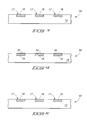
- FIG. 1 is a view of a semiconductor die and interposer at a stage of a prior art process for assembling an integrated circuit package.
- FIG. 2 is a view of the semiconductor die and interposer of FIG. 1 shown at a prior art processing stage subsequent to that of FIG. 1 .
- FIGS. 3-9 illustrates a process for preparing a semiconductor die for assembly into an integrated circuit package.
- FIGS. 10 and 11 illustrate a process for assembling an integrated circuit package comprising the semiconductor die of FIGS. 3-9 and an interposer.
- FIG. 12 shows a portion of an integrated circuit package comprising a bond between a bond pad region and an interconnect of an interposer in accordance with an embodiment.
- Some embodiments include methods of providing materials across bond pads to protect the pads during subsequent thermosonic bonding. Such materials may prevent, or at least substantially reduce, one or more of the problems discussed above in the “Background” section of this disclosure.
- An example embodiment for forming an integrated circuit package is described with reference to FIGS. 3-11 .
- FIG. 3 such illustrates a semiconductor die 50 comprising the base 14 and bond pad regions 16 discussed above with reference to the prior art semiconductor die 10 of FIG. 1 .
- the base may, as discussed above regarding FIG. 1 , comprise integrated circuitry containing memory, logic, sensors, etc.
- the bond pad regions 16 are shown to have outermost surfaces 17 .
- the bond pad regions may comprise, consist essentially of, or consist of aluminum or copper; and accordingly the outermost surfaces may comprise, consist essentially of, or consist of aluminum or copper. If the bond pad regions contain aluminum, a thin oxide of aluminum (not shown) may extend across the uppermost surfaces 17 at the processing stage of FIG. 3 .
- zinc-containing layers 52 are formed over bond pad regions 16 .
- the zinc-containing layers may be formed by first cleaning the bond pad regions with acid (for example, one or both of sulfuric acid and hydrofluoric acid) and/or base (for example, sodium hydroxide). Such cleaning forms a fresh surface for deposition of zinc, and may remove oxide. Subsequently, the surface may be exposed to zincate (in other words, to a zinc-containing solution, which may be, for example, cyanide-based, acid-based or alkaline-based) to deposit thin layers of zinc (which may be monolayers) across the surfaces of the bond pad regions.
- acid for example, one or both of sulfuric acid and hydrofluoric acid
- base for example, sodium hydroxide
- Such cleaning forms a fresh surface for deposition of zinc, and may remove oxide.
- the surface may be exposed to zincate (in other words, to a zinc-containing solution, which may be, for example, cyanide-based, acid-based or alkaline-based) to deposit thin layers
- the layers of zinc initially formed across the bond pad region surfaces may have relatively large grain sizes, and may be utilized as sacrificial layers to prepare the surfaces for subsequent deposition of zinc-containing layers with a smaller grain sizes. Accordingly, the first zinc-containing layers may be removed with an acid (for example, nitric acid) to again expose surfaces 17 of bond pad regions 16 ( FIG. 5 ), and then second zinc-containing layers 54 ( FIG. 6 ) may be formed by another exposure of the bond pad region surfaces to zincate.
- an acid for example, nitric acid
- the zinc-containing layers 54 are formed directly against the conductive material (for example, aluminum or copper) of the bond pad regions in the shown embodiment of FIG. 6 .
- Zinc-containing layers 54 may be considered examples of adhesion layers for adhering subsequently-formed layers (for instance, the layers 56 discussed below with reference to FIG. 7 ) to the bond pad regions.
- the zinc-containing layers are examples of adhesion layers, and other materials may be utilized for adhesion layers in other embodiments.
- zinc-containing layers work well for aluminum-containing surfaces, but may not work satisfactorily for copper-containing surfaces.
- palladium-containing adhesion layers may be utilized when the bond pad regions comprise copper.
- the bond pad regions may comprise materials other than copper or aluminum, and the adhesion layers may comprises materials other than, or in addition to, one or both of zinc and palladium.
- metal-containing layers 56 are formed over and directly against the adhesion layers 54 .
- the metal-containing layers may comprise one or more of Co, Cr, Ni, Pt, Ta, Ti, V and W; and may be doped with one or both of boron and phosphorous.
- layers 56 may comprise nickel deposited utilizing electroless deposition methodology.
- layers 56 may consist essentially of, or consist of such nickel; and in other embodiments layers 56 may consist essentially of, or consist of such nickel doped with phosphorous (the phosphorus may be present at a concentration of from about 7 atomic percent to about 11 atomic percent).
- electrically conductive layers 58 are formed over and directly against electrically conductive layers 56 , and balls 18 are formed directly against the conductive layers 58 .
- the electrically conductive layers 58 may, for example, comprise, consist essentially of, or consist of one or more of Ag, Au, Cu and Pd. Such materials may be formed by immersion methodologies, and may be doped with phosphorous or boron. For instance, the layers 58 may comprise Pd doped with phosphorous to a phosphorous concentration of from about 7 atomic percent to about 11 atomic percent.
- layers 56 may comprise, consist essentially of, or consist of nickel or nickel doped with phosphorus; and layers 58 may comprise, consist essentially of, or consist of gold.
- the layers 56 and 58 may together comprise a thickness of from about 0.1 micron to about 10 microns.
- the balls 18 utilized in FIG. 8 may comprise any of various electrically conductive materials, including, for example, copper or gold.
- the balls may thus comprise conventional compositions of the type described in the “Background” section of this disclosure, or may comprise non-conventional compositions.
- the balls will not comprise solder, and specifically will not comprise indium or tin.
- Layers 54 , 56 and 58 form electrically conductive stacks over bond pad regions 16 .
- the stacks extend across the entire upper surfaces of the bond pad regions, and may be considered protective electrically conductive caps formed across the bond pad regions.
- electrically conductive caps are shown to comprise only the three layers 54 , 56 and 58 in the embodiment of FIGS. 3-8 , in other embodiments one or more additional layers may be inserted between adhesion layer 54 and conductive layer 56 , and/or between conductive layer 56 and conductive layer 58 .
- the conductive stacks may comprise Ni/Pd/Au (with layers 56 and 58 being Ni and Au, respectively, and the layer of Pd being provided between them).
- conductive layers 58 are outward of conductive layers 56 relative to bond pad regions 16 ; the layers 56 may be referred to as inner conductive layers, and the layers 58 as outer conductive layers, in some embodiments.
- the layers 58 are shown to comprise outermost surfaces 59 .
- Balls 18 are bonded to the outermost surfaces 59 of layers 58 .
- the bonding of the balls to layers 58 may be accomplished with any suitable methodology, such as, for example, thermosonic bonding.
- Balls 18 may comprise, consist essentially of, or consist of copper or gold; and in some embodiments the outermost surfaces 59 may comprise, consist essentially of, or consist of copper or gold.
- deformable material 60 is formed across base 14 , across balls 18 , and across surfaces 59 of layers 58 .
- Deformable material 60 is ultimately utilized as an underfill material of a flip chip construction comprising semiconductor die 50 , and may, for example, comprise one or more of a non-conductive film, non-conductive paste, anisotropically conductive film (so-called z-axis film), anisotropically conductive paste (so-called z-axis paste), and organic solderability preservative (OSP).
- semiconductor die 50 is inverted and provided proximate another structure separate from the die, with such other structure corresponding to an interposer 12 of the type described above with reference to prior art FIGS. 1 and 2 .
- the interposer comprises the base 20 and interconnects 22 and 24 described above.
- the interconnects 22 may comprise, consist essentially of, or consist of copper, silver, palladium or gold; and comprise outer conductive surfaces 23 .
- the interconnects 22 may be considered to correspond to electrically conductive projections or bumps in some embodiments.
- die 50 is shown inverted in the embodiment of FIG. 10 , in other embodiments die 50 may remain in the orientation of FIG. 9 and interposer 12 may be inverted.
- underfill 60 is shown formed across a surface of the die, in other embodiments some or all of the underfill may be formed across surfaces associated with interposer 12 at the processing stage of FIG. 10 . For instance, if material 60 comprises OSP, such may be provided across outermost surfaces of interconnects 22 at the processing stage of FIG. 10 . In yet other embodiments, the underfill may be omitted, or provided at a processing stage subsequent to that of FIG. 10 .
- balls 18 are shown bonded to conductive layers 58 , in other embodiments the balls may be instead bonded to the interposer at the processing stage of FIG. 10 .
- interconnects 22 may be bonded to the balls utilizing vibrational and/or thermal energy.
- the vibrational energy may be provided to comprise a frequency of at least about one kilohertz, and the thermal energy may correspond to a temperature of at least about room temperature.
- the bonding may comprise thermosonic bonding at a temperature of from about room temperature (about 22° C.) to about 300° C.
- the bonding may be accomplished with the same combination of vibrational and/or thermal energy discussed above, but will bond the balls to surfaces 59 .
- balls 18 may be omitted, and the vibrational and/or thermal energy may be utilized to directly bond surfaces 23 of projections 22 to surfaces 59 of layers 58 .
- FIG. 11 shows surface 23 of interconnect 22 being planar, surface 59 of outer conductive layer 58 also being planar, and balls 18 being bonded to the planar surfaces. Such leaves gaps adjacent locations where the balls contact the planar surfaces, as shown in FIG. 12 .
- FIG. 12 shows a portion of an integrated circuit package 100 comprising the various structures and layers described above with reference to FIGS. 3-11 , but comprising a gap 102 identified between a surface of a ball 18 and a portion of surface 59 of outer conductive layer 58 .
- z-axis conductive material for example, anisotropically conductive film or paste
- underfill 60 so that the material 60 compressed between the surfaces of the ball and outer conductive layer 58 within gap 102 becomes conductive along the axis of compression (in other words, along a shown axis 110 extending within the gap between surface 59 and the ball).
- the conductivity of material 60 within the gap may then provide improved electrical connection between conductive layer 58 and interconnect 22 relative to that which would occur in the absence of conductivity of material 60 .
- Gaps similar to gap 52 are along all locations where planar surfaces 23 and 59 join to balls 18 .
Abstract
Description
Claims (9)
Priority Applications (1)
| Application Number | Priority Date | Filing Date | Title |
|---|---|---|---|
| US13/963,866 US8709866B2 (en) | 2007-05-17 | 2013-08-09 | Methods of forming integrated circuit packages |
Applications Claiming Priority (6)
| Application Number | Priority Date | Filing Date | Title |
|---|---|---|---|
| SG200703582 | 2007-05-17 | ||
| SG200703582-7A SG148056A1 (en) | 2007-05-17 | 2007-05-17 | Integrated circuit packages, methods of forming integrated circuit packages, and methods of assembling intgrated circuit packages |
| US11/770,451 US7700406B2 (en) | 2007-05-17 | 2007-06-28 | Methods of assembling integrated circuit packages |
| US12/715,293 US7977157B2 (en) | 2007-05-17 | 2010-03-01 | Methods of forming integrated circuit packages, and methods of assembling integrated circuit packages |
| US13/154,540 US8531031B2 (en) | 2007-05-17 | 2011-06-07 | Integrated circuit packages |
| US13/963,866 US8709866B2 (en) | 2007-05-17 | 2013-08-09 | Methods of forming integrated circuit packages |
Related Parent Applications (1)
| Application Number | Title | Priority Date | Filing Date |
|---|---|---|---|
| US13/154,540 Division US8531031B2 (en) | 2007-05-17 | 2011-06-07 | Integrated circuit packages |
Publications (2)
| Publication Number | Publication Date |
|---|---|
| US20130330882A1 US20130330882A1 (en) | 2013-12-12 |
| US8709866B2 true US8709866B2 (en) | 2014-04-29 |
Family
ID=40026686
Family Applications (4)
| Application Number | Title | Priority Date | Filing Date |
|---|---|---|---|
| US11/770,451 Active 2028-01-24 US7700406B2 (en) | 2007-05-17 | 2007-06-28 | Methods of assembling integrated circuit packages |
| US12/715,293 Active US7977157B2 (en) | 2007-05-17 | 2010-03-01 | Methods of forming integrated circuit packages, and methods of assembling integrated circuit packages |
| US13/154,540 Active 2028-02-29 US8531031B2 (en) | 2007-05-17 | 2011-06-07 | Integrated circuit packages |
| US13/963,866 Active US8709866B2 (en) | 2007-05-17 | 2013-08-09 | Methods of forming integrated circuit packages |
Family Applications Before (3)
| Application Number | Title | Priority Date | Filing Date |
|---|---|---|---|
| US11/770,451 Active 2028-01-24 US7700406B2 (en) | 2007-05-17 | 2007-06-28 | Methods of assembling integrated circuit packages |
| US12/715,293 Active US7977157B2 (en) | 2007-05-17 | 2010-03-01 | Methods of forming integrated circuit packages, and methods of assembling integrated circuit packages |
| US13/154,540 Active 2028-02-29 US8531031B2 (en) | 2007-05-17 | 2011-06-07 | Integrated circuit packages |
Country Status (4)
| Country | Link |
|---|---|
| US (4) | US7700406B2 (en) |
| SG (1) | SG148056A1 (en) |
| TW (1) | TW200913095A (en) |
| WO (1) | WO2008144153A1 (en) |
Cited By (1)
| Publication number | Priority date | Publication date | Assignee | Title |
|---|---|---|---|---|
| US10107662B2 (en) | 2015-01-30 | 2018-10-23 | Honeywell International Inc. | Sensor assembly |
Families Citing this family (9)
| Publication number | Priority date | Publication date | Assignee | Title |
|---|---|---|---|---|
| SG148056A1 (en) | 2007-05-17 | 2008-12-31 | Micron Technology Inc | Integrated circuit packages, methods of forming integrated circuit packages, and methods of assembling intgrated circuit packages |
| KR101041146B1 (en) * | 2009-09-02 | 2011-06-13 | 삼성모바일디스플레이주식회사 | Display device |
| CN102473650B (en) * | 2009-09-09 | 2014-09-24 | 株式会社日立制作所 | Connecting material, semiconductor device and method for manufacturing semiconductor device |
| US8394672B2 (en) * | 2010-08-14 | 2013-03-12 | Advanced Micro Devices, Inc. | Method of manufacturing and assembling semiconductor chips with offset pads |
| US8877630B1 (en) * | 2013-11-12 | 2014-11-04 | Chipmos Technologies Inc. | Semiconductor structure having a silver alloy bump body and manufacturing method thereof |
| US9368340B2 (en) * | 2014-06-02 | 2016-06-14 | Lam Research Corporation | Metallization of the wafer edge for optimized electroplating performance on resistive substrates |
| DE102017210585B3 (en) * | 2017-06-23 | 2018-09-27 | Robert Bosch Gmbh | Bondpad layer system, gas sensor and method for producing a gas sensor |
| US10629334B2 (en) * | 2017-09-20 | 2020-04-21 | Texas Instruments Incorporated | Nanostructure barrier for copper wire bonding |
| US10943880B2 (en) | 2019-05-16 | 2021-03-09 | Advanced Micro Devices, Inc. | Semiconductor chip with reduced pitch conductive pillars |
Citations (33)
| Publication number | Priority date | Publication date | Assignee | Title |
|---|---|---|---|---|
| GB2284928A (en) | 1993-12-17 | 1995-06-21 | Michael Lawrence Mcgeary | Laminated interconnect tape |
| US5804876A (en) | 1993-12-13 | 1998-09-08 | Micron Communications Inc. | Electronic circuit bonding interconnect component and flip chip interconnect bond |
| US6107109A (en) | 1997-12-18 | 2000-08-22 | Micron Technology, Inc. | Method for fabricating a semiconductor interconnect with laser machined electrical paths through substrate |
| US6270363B1 (en) | 1999-05-18 | 2001-08-07 | International Business Machines Corporation | Z-axis compressible polymer with fine metal matrix suspension |
| US6281046B1 (en) | 2000-04-25 | 2001-08-28 | Atmel Corporation | Method of forming an integrated circuit package at a wafer level |
| US20020100694A1 (en) | 2000-08-17 | 2002-08-01 | Morin Louis Charles | Electroplated aluminum parts and process of production |
| US6506672B1 (en) | 1999-06-30 | 2003-01-14 | University Of Maryland, College Park | Re-metallized aluminum bond pad, and method for making the same |
| US6556030B1 (en) | 1999-09-01 | 2003-04-29 | Micron Technology, Inc. | Method of forming an electrical contact |
| US20030094481A1 (en) | 2001-11-16 | 2003-05-22 | Matsushita Electric Industrial Co., Ltd. | Bump bonding method and apparatue |
| US20030127747A1 (en) | 2001-12-26 | 2003-07-10 | Ryoichi Kajiwara | Semiconductor device and manufacturing method thereof |
| US20030139004A1 (en) | 2001-03-12 | 2003-07-24 | Koji Yoshida | Method of manufacturing semiconductor device |
| US20040035840A1 (en) | 2002-08-23 | 2004-02-26 | Michel Koopmans | Component installation, removal, and replacement apparatus and method |
| US20040126928A1 (en) | 2000-06-02 | 2004-07-01 | Kinsman Larry D. | Method for fabricating a chip scale package using wafer level processing and devices resulting therefrom |
| US20040152292A1 (en) | 2002-09-19 | 2004-08-05 | Stephen Babinetz | Method and apparatus for forming bumps for semiconductor interconnections using a wire bonding machine |
| US20040164421A1 (en) | 2002-05-17 | 2004-08-26 | Tellkamp John P. | Metallic strain-absorbing layer for improved fatigue resistance of solder-attached devices |
| US20040229425A1 (en) | 2001-03-06 | 2004-11-18 | Katsumi Yamaguchi | Semiconductor device and bump formation method |
| US20050017372A1 (en) | 2003-07-22 | 2005-01-27 | Lua Edmund Koon Tian | Semiconductor substrates including I/O redistribution using wire bonds and anisotropically conductive film, methods of fabrication and assemblies including same |
| DE10343180A1 (en) | 2003-09-18 | 2005-04-14 | Robert Bosch Gmbh | Method for producing a high-temperature-resistant gold wire connection |
| US20050104207A1 (en) * | 2003-07-01 | 2005-05-19 | Dean Timothy B. | Corrosion-resistant bond pad and integrated device |
| US20050151268A1 (en) | 2004-01-08 | 2005-07-14 | Boyd William D. | Wafer-level assembly method for chip-size devices having flipped chips |
| US20050236709A1 (en) | 2002-08-27 | 2005-10-27 | Eng Meow K | Multiple chip semiconductor package and method of fabricating same |
| US20050285279A1 (en) * | 1999-07-30 | 2005-12-29 | Tongbi Jiang | Method and structure for manufacturing improved yield semiconductor packaged devices |
| US20060009029A1 (en) * | 2004-07-06 | 2006-01-12 | Agency For Science, Technology And Research | Wafer level through-hole plugging using mechanical forming technique |
| US20060012024A1 (en) | 2000-10-13 | 2006-01-19 | Bridge Semiconductor Corporation | Semiconductor chip assembly with metal containment wall and solder terminal |
| US20060092079A1 (en) | 2004-10-01 | 2006-05-04 | De Rochemont L P | Ceramic antenna module and methods of manufacture thereof |
| US7112471B2 (en) | 2002-08-28 | 2006-09-26 | Micron Technology, Inc. | Leadless packaging for image sensor devices and methods of assembly |
| US20060228825A1 (en) | 2005-04-08 | 2006-10-12 | Micron Technology, Inc. | Method and system for fabricating semiconductor components with through wire interconnects |
| WO2006124295A2 (en) | 2005-05-19 | 2006-11-23 | Micron Technology Inc. | Backside method and system for fabricating semiconductor components with conductive interconnects |
| US20070013067A1 (en) | 1999-01-29 | 2007-01-18 | Kazuto Nishida | Electronic component mounting method and apparatus |
| US20070020814A1 (en) | 2004-06-14 | 2007-01-25 | Hembree David R | Methods of underfilling and encapsulating semiconductor assemblies with materials having selected properties using stereolithography |
| US7427557B2 (en) | 2004-03-10 | 2008-09-23 | Unitive International Limited | Methods of forming bumps using barrier layers as etch masks |
| WO2008144153A1 (en) | 2007-05-17 | 2008-11-27 | Micron Technology, Inc. | Integrated circuit packages, methods of forming integrated circuit packages, and methods of assembling integrated circuit packages |
| US7671459B2 (en) | 2006-02-08 | 2010-03-02 | Micron Technologies, Inc. | Microelectronic devices, stacked microelectronic devices, and methods for manufacturing such devices |
Family Cites Families (3)
| Publication number | Priority date | Publication date | Assignee | Title |
|---|---|---|---|---|
| US6750551B1 (en) * | 1999-12-28 | 2004-06-15 | Intel Corporation | Direct BGA attachment without solder reflow |
| US6555412B1 (en) * | 1999-12-10 | 2003-04-29 | Micron Technology, Inc. | Packaged semiconductor chip and method of making same |
| JPWO2006064863A1 (en) * | 2004-12-17 | 2008-06-12 | イビデン株式会社 | Printed wiring board |
-
2007
- 2007-05-17 SG SG200703582-7A patent/SG148056A1/en unknown
- 2007-06-28 US US11/770,451 patent/US7700406B2/en active Active
-
2008
- 2008-04-22 WO PCT/US2008/061169 patent/WO2008144153A1/en active Application Filing
- 2008-05-12 TW TW097117471A patent/TW200913095A/en unknown
-
2010
- 2010-03-01 US US12/715,293 patent/US7977157B2/en active Active
-
2011
- 2011-06-07 US US13/154,540 patent/US8531031B2/en active Active
-
2013
- 2013-08-09 US US13/963,866 patent/US8709866B2/en active Active
Patent Citations (38)
| Publication number | Priority date | Publication date | Assignee | Title |
|---|---|---|---|---|
| US5804876A (en) | 1993-12-13 | 1998-09-08 | Micron Communications Inc. | Electronic circuit bonding interconnect component and flip chip interconnect bond |
| US6114239A (en) | 1993-12-13 | 2000-09-05 | Micron Communications, Inc. | Electronic circuit bonding interconnect component and flip chip interconnect bond |
| GB2284928A (en) | 1993-12-17 | 1995-06-21 | Michael Lawrence Mcgeary | Laminated interconnect tape |
| US6107109A (en) | 1997-12-18 | 2000-08-22 | Micron Technology, Inc. | Method for fabricating a semiconductor interconnect with laser machined electrical paths through substrate |
| US20070013067A1 (en) | 1999-01-29 | 2007-01-18 | Kazuto Nishida | Electronic component mounting method and apparatus |
| US6270363B1 (en) | 1999-05-18 | 2001-08-07 | International Business Machines Corporation | Z-axis compressible polymer with fine metal matrix suspension |
| US6506672B1 (en) | 1999-06-30 | 2003-01-14 | University Of Maryland, College Park | Re-metallized aluminum bond pad, and method for making the same |
| US20050285279A1 (en) * | 1999-07-30 | 2005-12-29 | Tongbi Jiang | Method and structure for manufacturing improved yield semiconductor packaged devices |
| US6556030B1 (en) | 1999-09-01 | 2003-04-29 | Micron Technology, Inc. | Method of forming an electrical contact |
| US6281046B1 (en) | 2000-04-25 | 2001-08-28 | Atmel Corporation | Method of forming an integrated circuit package at a wafer level |
| US20040126928A1 (en) | 2000-06-02 | 2004-07-01 | Kinsman Larry D. | Method for fabricating a chip scale package using wafer level processing and devices resulting therefrom |
| US20020100694A1 (en) | 2000-08-17 | 2002-08-01 | Morin Louis Charles | Electroplated aluminum parts and process of production |
| US20060012024A1 (en) | 2000-10-13 | 2006-01-19 | Bridge Semiconductor Corporation | Semiconductor chip assembly with metal containment wall and solder terminal |
| US20060014316A1 (en) | 2000-10-13 | 2006-01-19 | Bridge Semiconductor Corporation | Method of making a semiconductor chip assemby with a metal containment wall and a solder terminal |
| US20040229425A1 (en) | 2001-03-06 | 2004-11-18 | Katsumi Yamaguchi | Semiconductor device and bump formation method |
| US20030139004A1 (en) | 2001-03-12 | 2003-07-24 | Koji Yoshida | Method of manufacturing semiconductor device |
| US20030094481A1 (en) | 2001-11-16 | 2003-05-22 | Matsushita Electric Industrial Co., Ltd. | Bump bonding method and apparatue |
| US20030127747A1 (en) | 2001-12-26 | 2003-07-10 | Ryoichi Kajiwara | Semiconductor device and manufacturing method thereof |
| US20040164421A1 (en) | 2002-05-17 | 2004-08-26 | Tellkamp John P. | Metallic strain-absorbing layer for improved fatigue resistance of solder-attached devices |
| US20040035840A1 (en) | 2002-08-23 | 2004-02-26 | Michel Koopmans | Component installation, removal, and replacement apparatus and method |
| US20050236709A1 (en) | 2002-08-27 | 2005-10-27 | Eng Meow K | Multiple chip semiconductor package and method of fabricating same |
| US7112471B2 (en) | 2002-08-28 | 2006-09-26 | Micron Technology, Inc. | Leadless packaging for image sensor devices and methods of assembly |
| US20040152292A1 (en) | 2002-09-19 | 2004-08-05 | Stephen Babinetz | Method and apparatus for forming bumps for semiconductor interconnections using a wire bonding machine |
| US20050104207A1 (en) * | 2003-07-01 | 2005-05-19 | Dean Timothy B. | Corrosion-resistant bond pad and integrated device |
| US20050017372A1 (en) | 2003-07-22 | 2005-01-27 | Lua Edmund Koon Tian | Semiconductor substrates including I/O redistribution using wire bonds and anisotropically conductive film, methods of fabrication and assemblies including same |
| DE10343180A1 (en) | 2003-09-18 | 2005-04-14 | Robert Bosch Gmbh | Method for producing a high-temperature-resistant gold wire connection |
| US20050151268A1 (en) | 2004-01-08 | 2005-07-14 | Boyd William D. | Wafer-level assembly method for chip-size devices having flipped chips |
| US20080308931A1 (en) | 2004-03-10 | 2008-12-18 | Unitive International Limited | Electronic Structures Including Barrier Layers Defining Lips |
| US7427557B2 (en) | 2004-03-10 | 2008-09-23 | Unitive International Limited | Methods of forming bumps using barrier layers as etch masks |
| US20070020814A1 (en) | 2004-06-14 | 2007-01-25 | Hembree David R | Methods of underfilling and encapsulating semiconductor assemblies with materials having selected properties using stereolithography |
| US20060009029A1 (en) * | 2004-07-06 | 2006-01-12 | Agency For Science, Technology And Research | Wafer level through-hole plugging using mechanical forming technique |
| US20060092079A1 (en) | 2004-10-01 | 2006-05-04 | De Rochemont L P | Ceramic antenna module and methods of manufacture thereof |
| WO2006110266A2 (en) | 2005-04-08 | 2006-10-19 | Micron Technology, Inc. | Method and system for fabricating semiconductor components with through wire interconnects |
| US20060228825A1 (en) | 2005-04-08 | 2006-10-12 | Micron Technology, Inc. | Method and system for fabricating semiconductor components with through wire interconnects |
| US20060261446A1 (en) | 2005-05-19 | 2006-11-23 | Micron Technology, Inc. | Backside method and system for fabricating semiconductor components with conductive interconnects |
| WO2006124295A2 (en) | 2005-05-19 | 2006-11-23 | Micron Technology Inc. | Backside method and system for fabricating semiconductor components with conductive interconnects |
| US7671459B2 (en) | 2006-02-08 | 2010-03-02 | Micron Technologies, Inc. | Microelectronic devices, stacked microelectronic devices, and methods for manufacturing such devices |
| WO2008144153A1 (en) | 2007-05-17 | 2008-11-27 | Micron Technology, Inc. | Integrated circuit packages, methods of forming integrated circuit packages, and methods of assembling integrated circuit packages |
Non-Patent Citations (14)
| Title |
|---|
| Cheah, L.K., et al. "Thermosonic Flip Chip Assembly" Flip Chips Dot Com, Tutorial 9-Jun. 2007; reprinted Feb. 18, 2007; 7 pages. |
| Cheah, L.K., et al. "Thermosonic Flip Chip Assembly" Flip Chips Dot Com, Tutorial 9—Jun. 2007; reprinted Feb. 18, 2007; 7 pages. |
| Flip-Chip Assembly; http://www.siliconfareast.com/flipchipassy.htm; reprinted Feb. 16, 2007 2 pages. |
| Lee et al., "Thermosonic Bonding of Lead-Free Solder with Metal Bump for Flip-Chip Bonding", accepted (Aug. 18, 2004), Springer Boston, vol. 34, No. 1, 2005, pp. 96-102. |
| Riley, George A "Introduction to Flip Chip: What, Why How" . Flip Chips Dot Com, Tutorial 1-Oct. 2000 5 pages |
| Riley, George A "Introduction to Flip Chip: What, Why How" . Flip Chips Dot Com, Tutorial 1—Oct. 2000 5 pages |
| Riley, George A. "Electroless Nickel-Gold Flip Chip" Flip Chips Dot Com, Tutorial 7-Apr. 2001; reprinted Feb. 16, 2007; 4 pages. |
| Riley, George A. "Electroless Nickel-Gold Flip Chip" Flip Chips Dot Com, Tutorial 7—Apr. 2001; reprinted Feb. 16, 2007; 4 pages. |
| Riley, George A. "Stud Bump Flip Chip" Flip Chips Dot Com, Tutorial 3-Dec. 2000; 5 pages. |
| Riley, George A. "Stud Bump Flip Chip" Flip Chips Dot Com, Tutorial 3—Dec. 2000; 5 pages. |
| Riley, George A. "Under Bump Metallization (UBM)" Flip Chips Dot Com, Tutorial 11-Sep. 2001; reprinted Feb. 16, 2007; 3 pages. |
| Riley, George A. "Under Bump Metallization (UBM)" Flip Chips Dot Com, Tutorial 11—Sep. 2001; reprinted Feb. 16, 2007; 3 pages. |
| Roth Laurie, S. et al. "Stud Bump Bonding:" http://ap.pennet.com/Article/Article-Display.cfm reprinted Feb. 13, 2007 6 pages. |
| Roth Laurie, S. et al. "Stud Bump Bonding:" http://ap.pennet.com/Article/Article—Display.cfm reprinted Feb. 13, 2007 6 pages. |
Cited By (1)
| Publication number | Priority date | Publication date | Assignee | Title |
|---|---|---|---|---|
| US10107662B2 (en) | 2015-01-30 | 2018-10-23 | Honeywell International Inc. | Sensor assembly |
Also Published As
| Publication number | Publication date |
|---|---|
| SG148056A1 (en) | 2008-12-31 |
| US7977157B2 (en) | 2011-07-12 |
| US8531031B2 (en) | 2013-09-10 |
| TW200913095A (en) | 2009-03-16 |
| US7700406B2 (en) | 2010-04-20 |
| WO2008144153A1 (en) | 2008-11-27 |
| US20080284000A1 (en) | 2008-11-20 |
| US20100151630A1 (en) | 2010-06-17 |
| US20110233745A1 (en) | 2011-09-29 |
| US20130330882A1 (en) | 2013-12-12 |
Similar Documents
| Publication | Publication Date | Title |
|---|---|---|
| US8709866B2 (en) | Methods of forming integrated circuit packages | |
| JP5624649B2 (en) | Fusible input / output interconnect system and method for flip chip packaging with stud bumps attached to a substrate | |
| JP4742844B2 (en) | Manufacturing method of semiconductor device | |
| JP3735526B2 (en) | Semiconductor device and manufacturing method thereof | |
| US6346469B1 (en) | Semiconductor device and a process for forming the semiconductor device | |
| US7969004B2 (en) | Semiconductor device, method for mounting semiconductor device, and mounting structure of semiconductor device | |
| TW201128752A (en) | Integrated circuit packages and fabrication method thereof | |
| JP2009524927A (en) | Semiconductor chip on which solder bump is formed and method for manufacturing solder bump | |
| CN101295692B (en) | Semiconductor device | |
| JP2009283484A (en) | Semiconductor device, method for mounting semiconductor device, and mounting structure of semiconductor device | |
| US9013042B2 (en) | Interconnection structure for semiconductor package | |
| TWM397591U (en) | Bumping structure | |
| US7325716B2 (en) | Dense intermetallic compound layer | |
| CN101194361A (en) | Layer sequence and method of manufacturing a layer sequence | |
| US8110931B2 (en) | Wafer and semiconductor package | |
| JP2012190939A (en) | Semiconductor device and manufacturing method of the same | |
| US9601374B2 (en) | Semiconductor die assembly | |
| JP2004014854A (en) | Semiconductor device | |
| US20150247244A1 (en) | Thin nib or cob capping layer for non-noble metallic bonding landing pads | |
| JP2813409B2 (en) | Connection method of semiconductor chip | |
| US20090091036A1 (en) | Wafer structure with a buffer layer | |
| US9589877B2 (en) | Semiconductor device and method for manufacturing the same | |
| JP4668608B2 (en) | Semiconductor chip, semiconductor device using the same, and semiconductor chip manufacturing method | |
| TWI436465B (en) | Wire bonding structure, method for bonding a wire and method for manufacturing a semiconductor package | |
| TWI450347B (en) | Wire bonding structure |
Legal Events
| Date | Code | Title | Description |
|---|---|---|---|
| FEPP | Fee payment procedure |
Free format text: PAYOR NUMBER ASSIGNED (ORIGINAL EVENT CODE: ASPN); ENTITY STATUS OF PATENT OWNER: LARGE ENTITY |
|
| STCF | Information on status: patent grant |
Free format text: PATENTED CASE |
|
| AS | Assignment |
Owner name: U.S. BANK NATIONAL ASSOCIATION, AS COLLATERAL AGENT, CALIFORNIA Free format text: SECURITY INTEREST;ASSIGNOR:MICRON TECHNOLOGY, INC.;REEL/FRAME:038669/0001 Effective date: 20160426 Owner name: U.S. BANK NATIONAL ASSOCIATION, AS COLLATERAL AGEN Free format text: SECURITY INTEREST;ASSIGNOR:MICRON TECHNOLOGY, INC.;REEL/FRAME:038669/0001 Effective date: 20160426 |
|
| AS | Assignment |
Owner name: MORGAN STANLEY SENIOR FUNDING, INC., AS COLLATERAL AGENT, MARYLAND Free format text: PATENT SECURITY AGREEMENT;ASSIGNOR:MICRON TECHNOLOGY, INC.;REEL/FRAME:038954/0001 Effective date: 20160426 Owner name: MORGAN STANLEY SENIOR FUNDING, INC., AS COLLATERAL Free format text: PATENT SECURITY AGREEMENT;ASSIGNOR:MICRON TECHNOLOGY, INC.;REEL/FRAME:038954/0001 Effective date: 20160426 |
|
| AS | Assignment |
Owner name: U.S. BANK NATIONAL ASSOCIATION, AS COLLATERAL AGENT, CALIFORNIA Free format text: CORRECTIVE ASSIGNMENT TO CORRECT THE REPLACE ERRONEOUSLY FILED PATENT #7358718 WITH THE CORRECT PATENT #7358178 PREVIOUSLY RECORDED ON REEL 038669 FRAME 0001. ASSIGNOR(S) HEREBY CONFIRMS THE SECURITY INTEREST;ASSIGNOR:MICRON TECHNOLOGY, INC.;REEL/FRAME:043079/0001 Effective date: 20160426 Owner name: U.S. BANK NATIONAL ASSOCIATION, AS COLLATERAL AGEN Free format text: CORRECTIVE ASSIGNMENT TO CORRECT THE REPLACE ERRONEOUSLY FILED PATENT #7358718 WITH THE CORRECT PATENT #7358178 PREVIOUSLY RECORDED ON REEL 038669 FRAME 0001. ASSIGNOR(S) HEREBY CONFIRMS THE SECURITY INTEREST;ASSIGNOR:MICRON TECHNOLOGY, INC.;REEL/FRAME:043079/0001 Effective date: 20160426 |
|
| MAFP | Maintenance fee payment |
Free format text: PAYMENT OF MAINTENANCE FEE, 4TH YEAR, LARGE ENTITY (ORIGINAL EVENT CODE: M1551) Year of fee payment: 4 |
|
| AS | Assignment |
Owner name: JPMORGAN CHASE BANK, N.A., AS COLLATERAL AGENT, ILLINOIS Free format text: SECURITY INTEREST;ASSIGNORS:MICRON TECHNOLOGY, INC.;MICRON SEMICONDUCTOR PRODUCTS, INC.;REEL/FRAME:047540/0001 Effective date: 20180703 Owner name: JPMORGAN CHASE BANK, N.A., AS COLLATERAL AGENT, IL Free format text: SECURITY INTEREST;ASSIGNORS:MICRON TECHNOLOGY, INC.;MICRON SEMICONDUCTOR PRODUCTS, INC.;REEL/FRAME:047540/0001 Effective date: 20180703 |
|
| AS | Assignment |
Owner name: MICRON TECHNOLOGY, INC., IDAHO Free format text: RELEASE BY SECURED PARTY;ASSIGNOR:U.S. BANK NATIONAL ASSOCIATION, AS COLLATERAL AGENT;REEL/FRAME:047243/0001 Effective date: 20180629 |
|
| AS | Assignment |
Owner name: MICRON TECHNOLOGY, INC., IDAHO Free format text: RELEASE BY SECURED PARTY;ASSIGNOR:MORGAN STANLEY SENIOR FUNDING, INC., AS COLLATERAL AGENT;REEL/FRAME:050937/0001 Effective date: 20190731 |
|
| AS | Assignment |
Owner name: MICRON SEMICONDUCTOR PRODUCTS, INC., IDAHO Free format text: RELEASE BY SECURED PARTY;ASSIGNOR:JPMORGAN CHASE BANK, N.A., AS COLLATERAL AGENT;REEL/FRAME:051028/0001 Effective date: 20190731 Owner name: MICRON TECHNOLOGY, INC., IDAHO Free format text: RELEASE BY SECURED PARTY;ASSIGNOR:JPMORGAN CHASE BANK, N.A., AS COLLATERAL AGENT;REEL/FRAME:051028/0001 Effective date: 20190731 |
|
| MAFP | Maintenance fee payment |
Free format text: PAYMENT OF MAINTENANCE FEE, 8TH YEAR, LARGE ENTITY (ORIGINAL EVENT CODE: M1552); ENTITY STATUS OF PATENT OWNER: LARGE ENTITY Year of fee payment: 8 |