US8703540B2 - Chip-scale semiconductor die packaging method - Google Patents
Chip-scale semiconductor die packaging method Download PDFInfo
- Publication number
- US8703540B2 US8703540B2 US13/742,252 US201313742252A US8703540B2 US 8703540 B2 US8703540 B2 US 8703540B2 US 201313742252 A US201313742252 A US 201313742252A US 8703540 B2 US8703540 B2 US 8703540B2
- Authority
- US
- United States
- Prior art keywords
- chip
- die
- substrate
- scale frame
- coupling
- Prior art date
- Legal status (The legal status is an assumption and is not a legal conclusion. Google has not performed a legal analysis and makes no representation as to the accuracy of the status listed.)
- Expired - Fee Related
Links
Images


Classifications
-
- H—ELECTRICITY
- H01—ELECTRIC ELEMENTS
- H01L—SEMICONDUCTOR DEVICES NOT COVERED BY CLASS H10
- H01L21/00—Processes or apparatus adapted for the manufacture or treatment of semiconductor or solid state devices or of parts thereof
- H01L21/02—Manufacture or treatment of semiconductor devices or of parts thereof
- H01L21/04—Manufacture or treatment of semiconductor devices or of parts thereof the devices having at least one potential-jump barrier or surface barrier, e.g. PN junction, depletion layer or carrier concentration layer
- H01L21/50—Assembly of semiconductor devices using processes or apparatus not provided for in a single one of the subgroups H01L21/06 - H01L21/326, e.g. sealing of a cap to a base of a container
-
- H—ELECTRICITY
- H01—ELECTRIC ELEMENTS
- H01L—SEMICONDUCTOR DEVICES NOT COVERED BY CLASS H10
- H01L23/00—Details of semiconductor or other solid state devices
- H01L23/02—Containers; Seals
- H01L23/04—Containers; Seals characterised by the shape of the container or parts, e.g. caps, walls
-
- H—ELECTRICITY
- H01—ELECTRIC ELEMENTS
- H01L—SEMICONDUCTOR DEVICES NOT COVERED BY CLASS H10
- H01L23/00—Details of semiconductor or other solid state devices
- H01L23/12—Mountings, e.g. non-detachable insulating substrates
- H01L23/13—Mountings, e.g. non-detachable insulating substrates characterised by the shape
-
- H—ELECTRICITY
- H01—ELECTRIC ELEMENTS
- H01L—SEMICONDUCTOR DEVICES NOT COVERED BY CLASS H10
- H01L23/00—Details of semiconductor or other solid state devices
- H01L23/34—Arrangements for cooling, heating, ventilating or temperature compensation ; Temperature sensing arrangements
- H01L23/36—Selection of materials, or shaping, to facilitate cooling or heating, e.g. heatsinks
- H01L23/367—Cooling facilitated by shape of device
- H01L23/3675—Cooling facilitated by shape of device characterised by the shape of the housing
-
- H—ELECTRICITY
- H01—ELECTRIC ELEMENTS
- H01L—SEMICONDUCTOR DEVICES NOT COVERED BY CLASS H10
- H01L23/00—Details of semiconductor or other solid state devices
- H01L23/48—Arrangements for conducting electric current to or from the solid state body in operation, e.g. leads, terminal arrangements ; Selection of materials therefor
- H01L23/488—Arrangements for conducting electric current to or from the solid state body in operation, e.g. leads, terminal arrangements ; Selection of materials therefor consisting of soldered or bonded constructions
- H01L23/492—Bases or plates or solder therefor
-
- H—ELECTRICITY
- H01—ELECTRIC ELEMENTS
- H01L—SEMICONDUCTOR DEVICES NOT COVERED BY CLASS H10
- H01L25/00—Assemblies consisting of a plurality of individual semiconductor or other solid state devices ; Multistep manufacturing processes thereof
- H01L25/03—Assemblies consisting of a plurality of individual semiconductor or other solid state devices ; Multistep manufacturing processes thereof all the devices being of a type provided for in the same subgroup of groups H01L27/00 - H01L33/00, or in a single subclass of H10K, H10N, e.g. assemblies of rectifier diodes
- H01L25/04—Assemblies consisting of a plurality of individual semiconductor or other solid state devices ; Multistep manufacturing processes thereof all the devices being of a type provided for in the same subgroup of groups H01L27/00 - H01L33/00, or in a single subclass of H10K, H10N, e.g. assemblies of rectifier diodes the devices not having separate containers
- H01L25/065—Assemblies consisting of a plurality of individual semiconductor or other solid state devices ; Multistep manufacturing processes thereof all the devices being of a type provided for in the same subgroup of groups H01L27/00 - H01L33/00, or in a single subclass of H10K, H10N, e.g. assemblies of rectifier diodes the devices not having separate containers the devices being of a type provided for in group H01L27/00
- H01L25/0652—Assemblies consisting of a plurality of individual semiconductor or other solid state devices ; Multistep manufacturing processes thereof all the devices being of a type provided for in the same subgroup of groups H01L27/00 - H01L33/00, or in a single subclass of H10K, H10N, e.g. assemblies of rectifier diodes the devices not having separate containers the devices being of a type provided for in group H01L27/00 the devices being arranged next and on each other, i.e. mixed assemblies
-
- H—ELECTRICITY
- H01—ELECTRIC ELEMENTS
- H01L—SEMICONDUCTOR DEVICES NOT COVERED BY CLASS H10
- H01L2224/00—Indexing scheme for arrangements for connecting or disconnecting semiconductor or solid-state bodies and methods related thereto as covered by H01L24/00
- H01L2224/01—Means for bonding being attached to, or being formed on, the surface to be connected, e.g. chip-to-package, die-attach, "first-level" interconnects; Manufacturing methods related thereto
- H01L2224/02—Bonding areas; Manufacturing methods related thereto
- H01L2224/04—Structure, shape, material or disposition of the bonding areas prior to the connecting process
- H01L2224/05—Structure, shape, material or disposition of the bonding areas prior to the connecting process of an individual bonding area
- H01L2224/0554—External layer
- H01L2224/0555—Shape
- H01L2224/05552—Shape in top view
- H01L2224/05554—Shape in top view being square
-
- H—ELECTRICITY
- H01—ELECTRIC ELEMENTS
- H01L—SEMICONDUCTOR DEVICES NOT COVERED BY CLASS H10
- H01L2224/00—Indexing scheme for arrangements for connecting or disconnecting semiconductor or solid-state bodies and methods related thereto as covered by H01L24/00
- H01L2224/01—Means for bonding being attached to, or being formed on, the surface to be connected, e.g. chip-to-package, die-attach, "first-level" interconnects; Manufacturing methods related thereto
- H01L2224/10—Bump connectors; Manufacturing methods related thereto
- H01L2224/15—Structure, shape, material or disposition of the bump connectors after the connecting process
- H01L2224/16—Structure, shape, material or disposition of the bump connectors after the connecting process of an individual bump connector
- H01L2224/161—Disposition
- H01L2224/16151—Disposition the bump connector connecting between a semiconductor or solid-state body and an item not being a semiconductor or solid-state body, e.g. chip-to-substrate, chip-to-passive
- H01L2224/16221—Disposition the bump connector connecting between a semiconductor or solid-state body and an item not being a semiconductor or solid-state body, e.g. chip-to-substrate, chip-to-passive the body and the item being stacked
- H01L2224/16225—Disposition the bump connector connecting between a semiconductor or solid-state body and an item not being a semiconductor or solid-state body, e.g. chip-to-substrate, chip-to-passive the body and the item being stacked the item being non-metallic, e.g. insulating substrate with or without metallisation
- H01L2224/16235—Disposition the bump connector connecting between a semiconductor or solid-state body and an item not being a semiconductor or solid-state body, e.g. chip-to-substrate, chip-to-passive the body and the item being stacked the item being non-metallic, e.g. insulating substrate with or without metallisation the bump connector connecting to a via metallisation of the item
-
- H—ELECTRICITY
- H01—ELECTRIC ELEMENTS
- H01L—SEMICONDUCTOR DEVICES NOT COVERED BY CLASS H10
- H01L2224/00—Indexing scheme for arrangements for connecting or disconnecting semiconductor or solid-state bodies and methods related thereto as covered by H01L24/00
- H01L2224/01—Means for bonding being attached to, or being formed on, the surface to be connected, e.g. chip-to-package, die-attach, "first-level" interconnects; Manufacturing methods related thereto
- H01L2224/26—Layer connectors, e.g. plate connectors, solder or adhesive layers; Manufacturing methods related thereto
- H01L2224/28—Structure, shape, material or disposition of the layer connectors prior to the connecting process
- H01L2224/29—Structure, shape, material or disposition of the layer connectors prior to the connecting process of an individual layer connector
- H01L2224/29001—Core members of the layer connector
- H01L2224/29099—Material
- H01L2224/29198—Material with a principal constituent of the material being a combination of two or more materials in the form of a matrix with a filler, i.e. being a hybrid material, e.g. segmented structures, foams
- H01L2224/29199—Material of the matrix
- H01L2224/2929—Material of the matrix with a principal constituent of the material being a polymer, e.g. polyester, phenolic based polymer, epoxy
-
- H—ELECTRICITY
- H01—ELECTRIC ELEMENTS
- H01L—SEMICONDUCTOR DEVICES NOT COVERED BY CLASS H10
- H01L2224/00—Indexing scheme for arrangements for connecting or disconnecting semiconductor or solid-state bodies and methods related thereto as covered by H01L24/00
- H01L2224/01—Means for bonding being attached to, or being formed on, the surface to be connected, e.g. chip-to-package, die-attach, "first-level" interconnects; Manufacturing methods related thereto
- H01L2224/26—Layer connectors, e.g. plate connectors, solder or adhesive layers; Manufacturing methods related thereto
- H01L2224/28—Structure, shape, material or disposition of the layer connectors prior to the connecting process
- H01L2224/29—Structure, shape, material or disposition of the layer connectors prior to the connecting process of an individual layer connector
- H01L2224/29001—Core members of the layer connector
- H01L2224/29099—Material
- H01L2224/29198—Material with a principal constituent of the material being a combination of two or more materials in the form of a matrix with a filler, i.e. being a hybrid material, e.g. segmented structures, foams
- H01L2224/29298—Fillers
- H01L2224/29299—Base material
- H01L2224/293—Base material with a principal constituent of the material being a metal or a metalloid, e.g. boron [B], silicon [Si], germanium [Ge], arsenic [As], antimony [Sb], tellurium [Te] and polonium [Po], and alloys thereof
- H01L2224/29301—Base material with a principal constituent of the material being a metal or a metalloid, e.g. boron [B], silicon [Si], germanium [Ge], arsenic [As], antimony [Sb], tellurium [Te] and polonium [Po], and alloys thereof the principal constituent melting at a temperature of less than 400°C
- H01L2224/29311—Tin [Sn] as principal constituent
-
- H—ELECTRICITY
- H01—ELECTRIC ELEMENTS
- H01L—SEMICONDUCTOR DEVICES NOT COVERED BY CLASS H10
- H01L2224/00—Indexing scheme for arrangements for connecting or disconnecting semiconductor or solid-state bodies and methods related thereto as covered by H01L24/00
- H01L2224/01—Means for bonding being attached to, or being formed on, the surface to be connected, e.g. chip-to-package, die-attach, "first-level" interconnects; Manufacturing methods related thereto
- H01L2224/26—Layer connectors, e.g. plate connectors, solder or adhesive layers; Manufacturing methods related thereto
- H01L2224/28—Structure, shape, material or disposition of the layer connectors prior to the connecting process
- H01L2224/29—Structure, shape, material or disposition of the layer connectors prior to the connecting process of an individual layer connector
- H01L2224/29001—Core members of the layer connector
- H01L2224/29099—Material
- H01L2224/29198—Material with a principal constituent of the material being a combination of two or more materials in the form of a matrix with a filler, i.e. being a hybrid material, e.g. segmented structures, foams
- H01L2224/29298—Fillers
- H01L2224/29299—Base material
- H01L2224/293—Base material with a principal constituent of the material being a metal or a metalloid, e.g. boron [B], silicon [Si], germanium [Ge], arsenic [As], antimony [Sb], tellurium [Te] and polonium [Po], and alloys thereof
- H01L2224/29317—Base material with a principal constituent of the material being a metal or a metalloid, e.g. boron [B], silicon [Si], germanium [Ge], arsenic [As], antimony [Sb], tellurium [Te] and polonium [Po], and alloys thereof the principal constituent melting at a temperature of greater than or equal to 400°C and less than 950°C
- H01L2224/29324—Aluminium [Al] as principal constituent
-
- H—ELECTRICITY
- H01—ELECTRIC ELEMENTS
- H01L—SEMICONDUCTOR DEVICES NOT COVERED BY CLASS H10
- H01L2224/00—Indexing scheme for arrangements for connecting or disconnecting semiconductor or solid-state bodies and methods related thereto as covered by H01L24/00
- H01L2224/01—Means for bonding being attached to, or being formed on, the surface to be connected, e.g. chip-to-package, die-attach, "first-level" interconnects; Manufacturing methods related thereto
- H01L2224/26—Layer connectors, e.g. plate connectors, solder or adhesive layers; Manufacturing methods related thereto
- H01L2224/28—Structure, shape, material or disposition of the layer connectors prior to the connecting process
- H01L2224/29—Structure, shape, material or disposition of the layer connectors prior to the connecting process of an individual layer connector
- H01L2224/29001—Core members of the layer connector
- H01L2224/29099—Material
- H01L2224/29198—Material with a principal constituent of the material being a combination of two or more materials in the form of a matrix with a filler, i.e. being a hybrid material, e.g. segmented structures, foams
- H01L2224/29298—Fillers
- H01L2224/29299—Base material
- H01L2224/293—Base material with a principal constituent of the material being a metal or a metalloid, e.g. boron [B], silicon [Si], germanium [Ge], arsenic [As], antimony [Sb], tellurium [Te] and polonium [Po], and alloys thereof
- H01L2224/29338—Base material with a principal constituent of the material being a metal or a metalloid, e.g. boron [B], silicon [Si], germanium [Ge], arsenic [As], antimony [Sb], tellurium [Te] and polonium [Po], and alloys thereof the principal constituent melting at a temperature of greater than or equal to 950°C and less than 1550°C
- H01L2224/29347—Copper [Cu] as principal constituent
-
- H—ELECTRICITY
- H01—ELECTRIC ELEMENTS
- H01L—SEMICONDUCTOR DEVICES NOT COVERED BY CLASS H10
- H01L2224/00—Indexing scheme for arrangements for connecting or disconnecting semiconductor or solid-state bodies and methods related thereto as covered by H01L24/00
- H01L2224/01—Means for bonding being attached to, or being formed on, the surface to be connected, e.g. chip-to-package, die-attach, "first-level" interconnects; Manufacturing methods related thereto
- H01L2224/26—Layer connectors, e.g. plate connectors, solder or adhesive layers; Manufacturing methods related thereto
- H01L2224/31—Structure, shape, material or disposition of the layer connectors after the connecting process
- H01L2224/32—Structure, shape, material or disposition of the layer connectors after the connecting process of an individual layer connector
- H01L2224/321—Disposition
- H01L2224/32151—Disposition the layer connector connecting between a semiconductor or solid-state body and an item not being a semiconductor or solid-state body, e.g. chip-to-substrate, chip-to-passive
- H01L2224/32221—Disposition the layer connector connecting between a semiconductor or solid-state body and an item not being a semiconductor or solid-state body, e.g. chip-to-substrate, chip-to-passive the body and the item being stacked
- H01L2224/32225—Disposition the layer connector connecting between a semiconductor or solid-state body and an item not being a semiconductor or solid-state body, e.g. chip-to-substrate, chip-to-passive the body and the item being stacked the item being non-metallic, e.g. insulating substrate with or without metallisation
-
- H—ELECTRICITY
- H01—ELECTRIC ELEMENTS
- H01L—SEMICONDUCTOR DEVICES NOT COVERED BY CLASS H10
- H01L2224/00—Indexing scheme for arrangements for connecting or disconnecting semiconductor or solid-state bodies and methods related thereto as covered by H01L24/00
- H01L2224/01—Means for bonding being attached to, or being formed on, the surface to be connected, e.g. chip-to-package, die-attach, "first-level" interconnects; Manufacturing methods related thereto
- H01L2224/26—Layer connectors, e.g. plate connectors, solder or adhesive layers; Manufacturing methods related thereto
- H01L2224/31—Structure, shape, material or disposition of the layer connectors after the connecting process
- H01L2224/32—Structure, shape, material or disposition of the layer connectors after the connecting process of an individual layer connector
- H01L2224/321—Disposition
- H01L2224/32151—Disposition the layer connector connecting between a semiconductor or solid-state body and an item not being a semiconductor or solid-state body, e.g. chip-to-substrate, chip-to-passive
- H01L2224/32221—Disposition the layer connector connecting between a semiconductor or solid-state body and an item not being a semiconductor or solid-state body, e.g. chip-to-substrate, chip-to-passive the body and the item being stacked
- H01L2224/32245—Disposition the layer connector connecting between a semiconductor or solid-state body and an item not being a semiconductor or solid-state body, e.g. chip-to-substrate, chip-to-passive the body and the item being stacked the item being metallic
-
- H—ELECTRICITY
- H01—ELECTRIC ELEMENTS
- H01L—SEMICONDUCTOR DEVICES NOT COVERED BY CLASS H10
- H01L2224/00—Indexing scheme for arrangements for connecting or disconnecting semiconductor or solid-state bodies and methods related thereto as covered by H01L24/00
- H01L2224/01—Means for bonding being attached to, or being formed on, the surface to be connected, e.g. chip-to-package, die-attach, "first-level" interconnects; Manufacturing methods related thereto
- H01L2224/42—Wire connectors; Manufacturing methods related thereto
- H01L2224/47—Structure, shape, material or disposition of the wire connectors after the connecting process
- H01L2224/48—Structure, shape, material or disposition of the wire connectors after the connecting process of an individual wire connector
- H01L2224/4805—Shape
- H01L2224/4809—Loop shape
- H01L2224/48091—Arched
-
- H—ELECTRICITY
- H01—ELECTRIC ELEMENTS
- H01L—SEMICONDUCTOR DEVICES NOT COVERED BY CLASS H10
- H01L2224/00—Indexing scheme for arrangements for connecting or disconnecting semiconductor or solid-state bodies and methods related thereto as covered by H01L24/00
- H01L2224/01—Means for bonding being attached to, or being formed on, the surface to be connected, e.g. chip-to-package, die-attach, "first-level" interconnects; Manufacturing methods related thereto
- H01L2224/42—Wire connectors; Manufacturing methods related thereto
- H01L2224/47—Structure, shape, material or disposition of the wire connectors after the connecting process
- H01L2224/48—Structure, shape, material or disposition of the wire connectors after the connecting process of an individual wire connector
- H01L2224/481—Disposition
- H01L2224/48151—Connecting between a semiconductor or solid-state body and an item not being a semiconductor or solid-state body, e.g. chip-to-substrate, chip-to-passive
- H01L2224/48221—Connecting between a semiconductor or solid-state body and an item not being a semiconductor or solid-state body, e.g. chip-to-substrate, chip-to-passive the body and the item being stacked
- H01L2224/48225—Connecting between a semiconductor or solid-state body and an item not being a semiconductor or solid-state body, e.g. chip-to-substrate, chip-to-passive the body and the item being stacked the item being non-metallic, e.g. insulating substrate with or without metallisation
- H01L2224/48227—Connecting between a semiconductor or solid-state body and an item not being a semiconductor or solid-state body, e.g. chip-to-substrate, chip-to-passive the body and the item being stacked the item being non-metallic, e.g. insulating substrate with or without metallisation connecting the wire to a bond pad of the item
-
- H—ELECTRICITY
- H01—ELECTRIC ELEMENTS
- H01L—SEMICONDUCTOR DEVICES NOT COVERED BY CLASS H10
- H01L2224/00—Indexing scheme for arrangements for connecting or disconnecting semiconductor or solid-state bodies and methods related thereto as covered by H01L24/00
- H01L2224/01—Means for bonding being attached to, or being formed on, the surface to be connected, e.g. chip-to-package, die-attach, "first-level" interconnects; Manufacturing methods related thereto
- H01L2224/42—Wire connectors; Manufacturing methods related thereto
- H01L2224/47—Structure, shape, material or disposition of the wire connectors after the connecting process
- H01L2224/49—Structure, shape, material or disposition of the wire connectors after the connecting process of a plurality of wire connectors
- H01L2224/491—Disposition
- H01L2224/4912—Layout
- H01L2224/49171—Fan-out arrangements
-
- H—ELECTRICITY
- H01—ELECTRIC ELEMENTS
- H01L—SEMICONDUCTOR DEVICES NOT COVERED BY CLASS H10
- H01L2224/00—Indexing scheme for arrangements for connecting or disconnecting semiconductor or solid-state bodies and methods related thereto as covered by H01L24/00
- H01L2224/73—Means for bonding being of different types provided for in two or more of groups H01L2224/10, H01L2224/18, H01L2224/26, H01L2224/34, H01L2224/42, H01L2224/50, H01L2224/63, H01L2224/71
- H01L2224/732—Location after the connecting process
- H01L2224/73201—Location after the connecting process on the same surface
- H01L2224/73203—Bump and layer connectors
- H01L2224/73204—Bump and layer connectors the bump connector being embedded into the layer connector
-
- H—ELECTRICITY
- H01—ELECTRIC ELEMENTS
- H01L—SEMICONDUCTOR DEVICES NOT COVERED BY CLASS H10
- H01L2224/00—Indexing scheme for arrangements for connecting or disconnecting semiconductor or solid-state bodies and methods related thereto as covered by H01L24/00
- H01L2224/73—Means for bonding being of different types provided for in two or more of groups H01L2224/10, H01L2224/18, H01L2224/26, H01L2224/34, H01L2224/42, H01L2224/50, H01L2224/63, H01L2224/71
- H01L2224/732—Location after the connecting process
- H01L2224/73251—Location after the connecting process on different surfaces
- H01L2224/73253—Bump and layer connectors
-
- H—ELECTRICITY
- H01—ELECTRIC ELEMENTS
- H01L—SEMICONDUCTOR DEVICES NOT COVERED BY CLASS H10
- H01L2224/00—Indexing scheme for arrangements for connecting or disconnecting semiconductor or solid-state bodies and methods related thereto as covered by H01L24/00
- H01L2224/73—Means for bonding being of different types provided for in two or more of groups H01L2224/10, H01L2224/18, H01L2224/26, H01L2224/34, H01L2224/42, H01L2224/50, H01L2224/63, H01L2224/71
- H01L2224/732—Location after the connecting process
- H01L2224/73251—Location after the connecting process on different surfaces
- H01L2224/73265—Layer and wire connectors
-
- H—ELECTRICITY
- H01—ELECTRIC ELEMENTS
- H01L—SEMICONDUCTOR DEVICES NOT COVERED BY CLASS H10
- H01L2225/00—Details relating to assemblies covered by the group H01L25/00 but not provided for in its subgroups
- H01L2225/03—All the devices being of a type provided for in the same subgroup of groups H01L27/00 - H01L33/648 and H10K99/00
- H01L2225/04—All the devices being of a type provided for in the same subgroup of groups H01L27/00 - H01L33/648 and H10K99/00 the devices not having separate containers
- H01L2225/065—All the devices being of a type provided for in the same subgroup of groups H01L27/00 - H01L33/648 and H10K99/00 the devices not having separate containers the devices being of a type provided for in group H01L27/00
- H01L2225/06503—Stacked arrangements of devices
- H01L2225/0651—Wire or wire-like electrical connections from device to substrate
-
- H—ELECTRICITY
- H01—ELECTRIC ELEMENTS
- H01L—SEMICONDUCTOR DEVICES NOT COVERED BY CLASS H10
- H01L2225/00—Details relating to assemblies covered by the group H01L25/00 but not provided for in its subgroups
- H01L2225/03—All the devices being of a type provided for in the same subgroup of groups H01L27/00 - H01L33/648 and H10K99/00
- H01L2225/04—All the devices being of a type provided for in the same subgroup of groups H01L27/00 - H01L33/648 and H10K99/00 the devices not having separate containers
- H01L2225/065—All the devices being of a type provided for in the same subgroup of groups H01L27/00 - H01L33/648 and H10K99/00 the devices not having separate containers the devices being of a type provided for in group H01L27/00
- H01L2225/06503—Stacked arrangements of devices
- H01L2225/06517—Bump or bump-like direct electrical connections from device to substrate
-
- H—ELECTRICITY
- H01—ELECTRIC ELEMENTS
- H01L—SEMICONDUCTOR DEVICES NOT COVERED BY CLASS H10
- H01L2225/00—Details relating to assemblies covered by the group H01L25/00 but not provided for in its subgroups
- H01L2225/03—All the devices being of a type provided for in the same subgroup of groups H01L27/00 - H01L33/648 and H10K99/00
- H01L2225/04—All the devices being of a type provided for in the same subgroup of groups H01L27/00 - H01L33/648 and H10K99/00 the devices not having separate containers
- H01L2225/065—All the devices being of a type provided for in the same subgroup of groups H01L27/00 - H01L33/648 and H10K99/00 the devices not having separate containers the devices being of a type provided for in group H01L27/00
- H01L2225/06503—Stacked arrangements of devices
- H01L2225/06589—Thermal management, e.g. cooling
-
- H—ELECTRICITY
- H01—ELECTRIC ELEMENTS
- H01L—SEMICONDUCTOR DEVICES NOT COVERED BY CLASS H10
- H01L23/00—Details of semiconductor or other solid state devices
- H01L23/02—Containers; Seals
- H01L23/04—Containers; Seals characterised by the shape of the container or parts, e.g. caps, walls
- H01L23/053—Containers; Seals characterised by the shape of the container or parts, e.g. caps, walls the container being a hollow construction and having an insulating or insulated base as a mounting for the semiconductor body
- H01L23/055—Containers; Seals characterised by the shape of the container or parts, e.g. caps, walls the container being a hollow construction and having an insulating or insulated base as a mounting for the semiconductor body the leads having a passage through the base
-
- H—ELECTRICITY
- H01—ELECTRIC ELEMENTS
- H01L—SEMICONDUCTOR DEVICES NOT COVERED BY CLASS H10
- H01L23/00—Details of semiconductor or other solid state devices
- H01L23/552—Protection against radiation, e.g. light or electromagnetic waves
-
- H—ELECTRICITY
- H01—ELECTRIC ELEMENTS
- H01L—SEMICONDUCTOR DEVICES NOT COVERED BY CLASS H10
- H01L24/00—Arrangements for connecting or disconnecting semiconductor or solid-state bodies; Methods or apparatus related thereto
- H01L24/01—Means for bonding being attached to, or being formed on, the surface to be connected, e.g. chip-to-package, die-attach, "first-level" interconnects; Manufacturing methods related thereto
- H01L24/10—Bump connectors ; Manufacturing methods related thereto
- H01L24/15—Structure, shape, material or disposition of the bump connectors after the connecting process
- H01L24/16—Structure, shape, material or disposition of the bump connectors after the connecting process of an individual bump connector
-
- H—ELECTRICITY
- H01—ELECTRIC ELEMENTS
- H01L—SEMICONDUCTOR DEVICES NOT COVERED BY CLASS H10
- H01L24/00—Arrangements for connecting or disconnecting semiconductor or solid-state bodies; Methods or apparatus related thereto
- H01L24/01—Means for bonding being attached to, or being formed on, the surface to be connected, e.g. chip-to-package, die-attach, "first-level" interconnects; Manufacturing methods related thereto
- H01L24/26—Layer connectors, e.g. plate connectors, solder or adhesive layers; Manufacturing methods related thereto
- H01L24/31—Structure, shape, material or disposition of the layer connectors after the connecting process
- H01L24/32—Structure, shape, material or disposition of the layer connectors after the connecting process of an individual layer connector
-
- H—ELECTRICITY
- H01—ELECTRIC ELEMENTS
- H01L—SEMICONDUCTOR DEVICES NOT COVERED BY CLASS H10
- H01L24/00—Arrangements for connecting or disconnecting semiconductor or solid-state bodies; Methods or apparatus related thereto
- H01L24/01—Means for bonding being attached to, or being formed on, the surface to be connected, e.g. chip-to-package, die-attach, "first-level" interconnects; Manufacturing methods related thereto
- H01L24/42—Wire connectors; Manufacturing methods related thereto
- H01L24/47—Structure, shape, material or disposition of the wire connectors after the connecting process
- H01L24/48—Structure, shape, material or disposition of the wire connectors after the connecting process of an individual wire connector
-
- H—ELECTRICITY
- H01—ELECTRIC ELEMENTS
- H01L—SEMICONDUCTOR DEVICES NOT COVERED BY CLASS H10
- H01L24/00—Arrangements for connecting or disconnecting semiconductor or solid-state bodies; Methods or apparatus related thereto
- H01L24/01—Means for bonding being attached to, or being formed on, the surface to be connected, e.g. chip-to-package, die-attach, "first-level" interconnects; Manufacturing methods related thereto
- H01L24/42—Wire connectors; Manufacturing methods related thereto
- H01L24/47—Structure, shape, material or disposition of the wire connectors after the connecting process
- H01L24/49—Structure, shape, material or disposition of the wire connectors after the connecting process of a plurality of wire connectors
-
- H—ELECTRICITY
- H01—ELECTRIC ELEMENTS
- H01L—SEMICONDUCTOR DEVICES NOT COVERED BY CLASS H10
- H01L24/00—Arrangements for connecting or disconnecting semiconductor or solid-state bodies; Methods or apparatus related thereto
- H01L24/73—Means for bonding being of different types provided for in two or more of groups H01L24/10, H01L24/18, H01L24/26, H01L24/34, H01L24/42, H01L24/50, H01L24/63, H01L24/71
-
- H—ELECTRICITY
- H01—ELECTRIC ELEMENTS
- H01L—SEMICONDUCTOR DEVICES NOT COVERED BY CLASS H10
- H01L2924/00—Indexing scheme for arrangements or methods for connecting or disconnecting semiconductor or solid-state bodies as covered by H01L24/00
- H01L2924/0001—Technical content checked by a classifier
- H01L2924/00014—Technical content checked by a classifier the subject-matter covered by the group, the symbol of which is combined with the symbol of this group, being disclosed without further technical details
-
- H—ELECTRICITY
- H01—ELECTRIC ELEMENTS
- H01L—SEMICONDUCTOR DEVICES NOT COVERED BY CLASS H10
- H01L2924/00—Indexing scheme for arrangements or methods for connecting or disconnecting semiconductor or solid-state bodies as covered by H01L24/00
- H01L2924/095—Indexing scheme for arrangements or methods for connecting or disconnecting semiconductor or solid-state bodies as covered by H01L24/00 with a principal constituent of the material being a combination of two or more materials provided in the groups H01L2924/013 - H01L2924/0715
- H01L2924/097—Glass-ceramics, e.g. devitrified glass
- H01L2924/09701—Low temperature co-fired ceramic [LTCC]
-
- H—ELECTRICITY
- H01—ELECTRIC ELEMENTS
- H01L—SEMICONDUCTOR DEVICES NOT COVERED BY CLASS H10
- H01L2924/00—Indexing scheme for arrangements or methods for connecting or disconnecting semiconductor or solid-state bodies as covered by H01L24/00
- H01L2924/10—Details of semiconductor or other solid state devices to be connected
- H01L2924/102—Material of the semiconductor or solid state bodies
- H01L2924/1025—Semiconducting materials
- H01L2924/10251—Elemental semiconductors, i.e. Group IV
- H01L2924/10253—Silicon [Si]
-
- H—ELECTRICITY
- H01—ELECTRIC ELEMENTS
- H01L—SEMICONDUCTOR DEVICES NOT COVERED BY CLASS H10
- H01L2924/00—Indexing scheme for arrangements or methods for connecting or disconnecting semiconductor or solid-state bodies as covered by H01L24/00
- H01L2924/10—Details of semiconductor or other solid state devices to be connected
- H01L2924/102—Material of the semiconductor or solid state bodies
- H01L2924/1025—Semiconducting materials
- H01L2924/1026—Compound semiconductors
- H01L2924/1027—IV
- H01L2924/10271—Silicon-germanium [SiGe]
-
- H—ELECTRICITY
- H01—ELECTRIC ELEMENTS
- H01L—SEMICONDUCTOR DEVICES NOT COVERED BY CLASS H10
- H01L2924/00—Indexing scheme for arrangements or methods for connecting or disconnecting semiconductor or solid-state bodies as covered by H01L24/00
- H01L2924/10—Details of semiconductor or other solid state devices to be connected
- H01L2924/102—Material of the semiconductor or solid state bodies
- H01L2924/1025—Semiconducting materials
- H01L2924/1026—Compound semiconductors
- H01L2924/1032—III-V
- H01L2924/10329—Gallium arsenide [GaAs]
-
- H—ELECTRICITY
- H01—ELECTRIC ELEMENTS
- H01L—SEMICONDUCTOR DEVICES NOT COVERED BY CLASS H10
- H01L2924/00—Indexing scheme for arrangements or methods for connecting or disconnecting semiconductor or solid-state bodies as covered by H01L24/00
- H01L2924/10—Details of semiconductor or other solid state devices to be connected
- H01L2924/102—Material of the semiconductor or solid state bodies
- H01L2924/1025—Semiconducting materials
- H01L2924/1026—Compound semiconductors
- H01L2924/1032—III-V
- H01L2924/10335—Indium phosphide [InP]
-
- H—ELECTRICITY
- H01—ELECTRIC ELEMENTS
- H01L—SEMICONDUCTOR DEVICES NOT COVERED BY CLASS H10
- H01L2924/00—Indexing scheme for arrangements or methods for connecting or disconnecting semiconductor or solid-state bodies as covered by H01L24/00
- H01L2924/10—Details of semiconductor or other solid state devices to be connected
- H01L2924/102—Material of the semiconductor or solid state bodies
- H01L2924/1025—Semiconducting materials
- H01L2924/1026—Compound semiconductors
- H01L2924/1032—III-V
- H01L2924/10338—Indium gallium phosphide [InGaP]
-
- H—ELECTRICITY
- H01—ELECTRIC ELEMENTS
- H01L—SEMICONDUCTOR DEVICES NOT COVERED BY CLASS H10
- H01L2924/00—Indexing scheme for arrangements or methods for connecting or disconnecting semiconductor or solid-state bodies as covered by H01L24/00
- H01L2924/10—Details of semiconductor or other solid state devices to be connected
- H01L2924/11—Device type
- H01L2924/12—Passive devices, e.g. 2 terminal devices
- H01L2924/1204—Optical Diode
- H01L2924/12041—LED
-
- H—ELECTRICITY
- H01—ELECTRIC ELEMENTS
- H01L—SEMICONDUCTOR DEVICES NOT COVERED BY CLASS H10
- H01L2924/00—Indexing scheme for arrangements or methods for connecting or disconnecting semiconductor or solid-state bodies as covered by H01L24/00
- H01L2924/10—Details of semiconductor or other solid state devices to be connected
- H01L2924/11—Device type
- H01L2924/13—Discrete devices, e.g. 3 terminal devices
- H01L2924/1304—Transistor
- H01L2924/1305—Bipolar Junction Transistor [BJT]
-
- H—ELECTRICITY
- H01—ELECTRIC ELEMENTS
- H01L—SEMICONDUCTOR DEVICES NOT COVERED BY CLASS H10
- H01L2924/00—Indexing scheme for arrangements or methods for connecting or disconnecting semiconductor or solid-state bodies as covered by H01L24/00
- H01L2924/10—Details of semiconductor or other solid state devices to be connected
- H01L2924/11—Device type
- H01L2924/14—Integrated circuits
-
- H—ELECTRICITY
- H01—ELECTRIC ELEMENTS
- H01L—SEMICONDUCTOR DEVICES NOT COVERED BY CLASS H10
- H01L2924/00—Indexing scheme for arrangements or methods for connecting or disconnecting semiconductor or solid-state bodies as covered by H01L24/00
- H01L2924/15—Details of package parts other than the semiconductor or other solid state devices to be connected
- H01L2924/151—Die mounting substrate
- H01L2924/1517—Multilayer substrate
- H01L2924/15172—Fan-out arrangement of the internal vias
- H01L2924/15174—Fan-out arrangement of the internal vias in different layers of the multilayer substrate
-
- H—ELECTRICITY
- H01—ELECTRIC ELEMENTS
- H01L—SEMICONDUCTOR DEVICES NOT COVERED BY CLASS H10
- H01L2924/00—Indexing scheme for arrangements or methods for connecting or disconnecting semiconductor or solid-state bodies as covered by H01L24/00
- H01L2924/15—Details of package parts other than the semiconductor or other solid state devices to be connected
- H01L2924/151—Die mounting substrate
- H01L2924/1517—Multilayer substrate
- H01L2924/15182—Fan-in arrangement of the internal vias
- H01L2924/15184—Fan-in arrangement of the internal vias in different layers of the multilayer substrate
-
- H—ELECTRICITY
- H01—ELECTRIC ELEMENTS
- H01L—SEMICONDUCTOR DEVICES NOT COVERED BY CLASS H10
- H01L2924/00—Indexing scheme for arrangements or methods for connecting or disconnecting semiconductor or solid-state bodies as covered by H01L24/00
- H01L2924/15—Details of package parts other than the semiconductor or other solid state devices to be connected
- H01L2924/151—Die mounting substrate
- H01L2924/1517—Multilayer substrate
- H01L2924/15192—Resurf arrangement of the internal vias
-
- H—ELECTRICITY
- H01—ELECTRIC ELEMENTS
- H01L—SEMICONDUCTOR DEVICES NOT COVERED BY CLASS H10
- H01L2924/00—Indexing scheme for arrangements or methods for connecting or disconnecting semiconductor or solid-state bodies as covered by H01L24/00
- H01L2924/15—Details of package parts other than the semiconductor or other solid state devices to be connected
- H01L2924/151—Die mounting substrate
- H01L2924/153—Connection portion
- H01L2924/1531—Connection portion the connection portion being formed only on the surface of the substrate opposite to the die mounting surface
- H01L2924/15311—Connection portion the connection portion being formed only on the surface of the substrate opposite to the die mounting surface being a ball array, e.g. BGA
-
- H—ELECTRICITY
- H01—ELECTRIC ELEMENTS
- H01L—SEMICONDUCTOR DEVICES NOT COVERED BY CLASS H10
- H01L2924/00—Indexing scheme for arrangements or methods for connecting or disconnecting semiconductor or solid-state bodies as covered by H01L24/00
- H01L2924/15—Details of package parts other than the semiconductor or other solid state devices to be connected
- H01L2924/151—Die mounting substrate
- H01L2924/153—Connection portion
- H01L2924/1532—Connection portion the connection portion being formed on the die mounting surface of the substrate
-
- H—ELECTRICITY
- H01—ELECTRIC ELEMENTS
- H01L—SEMICONDUCTOR DEVICES NOT COVERED BY CLASS H10
- H01L2924/00—Indexing scheme for arrangements or methods for connecting or disconnecting semiconductor or solid-state bodies as covered by H01L24/00
- H01L2924/15—Details of package parts other than the semiconductor or other solid state devices to be connected
- H01L2924/161—Cap
- H01L2924/1615—Shape
- H01L2924/16152—Cap comprising a cavity for hosting the device, e.g. U-shaped cap
-
- H—ELECTRICITY
- H01—ELECTRIC ELEMENTS
- H01L—SEMICONDUCTOR DEVICES NOT COVERED BY CLASS H10
- H01L2924/00—Indexing scheme for arrangements or methods for connecting or disconnecting semiconductor or solid-state bodies as covered by H01L24/00
- H01L2924/15—Details of package parts other than the semiconductor or other solid state devices to be connected
- H01L2924/161—Cap
- H01L2924/1615—Shape
- H01L2924/16196—Cap forming a cavity, e.g. being a curved metal foil
-
- H—ELECTRICITY
- H01—ELECTRIC ELEMENTS
- H01L—SEMICONDUCTOR DEVICES NOT COVERED BY CLASS H10
- H01L2924/00—Indexing scheme for arrangements or methods for connecting or disconnecting semiconductor or solid-state bodies as covered by H01L24/00
- H01L2924/15—Details of package parts other than the semiconductor or other solid state devices to be connected
- H01L2924/161—Cap
- H01L2924/162—Disposition
- H01L2924/16251—Connecting to an item not being a semiconductor or solid-state body, e.g. cap-to-substrate
-
- H—ELECTRICITY
- H01—ELECTRIC ELEMENTS
- H01L—SEMICONDUCTOR DEVICES NOT COVERED BY CLASS H10
- H01L2924/00—Indexing scheme for arrangements or methods for connecting or disconnecting semiconductor or solid-state bodies as covered by H01L24/00
- H01L2924/15—Details of package parts other than the semiconductor or other solid state devices to be connected
- H01L2924/161—Cap
- H01L2924/166—Material
- H01L2924/167—Material with a principal constituent of the material being a metal or a metalloid, e.g. boron [B], silicon [Si], germanium [Ge], arsenic [As], antimony [Sb], tellurium [Te] and polonium [Po], and alloys thereof
-
- H—ELECTRICITY
- H01—ELECTRIC ELEMENTS
- H01L—SEMICONDUCTOR DEVICES NOT COVERED BY CLASS H10
- H01L2924/00—Indexing scheme for arrangements or methods for connecting or disconnecting semiconductor or solid-state bodies as covered by H01L24/00
- H01L2924/15—Details of package parts other than the semiconductor or other solid state devices to be connected
- H01L2924/161—Cap
- H01L2924/166—Material
- H01L2924/16786—Material with a principal constituent of the material being a non metallic, non metalloid inorganic material
- H01L2924/16787—Ceramics, e.g. crystalline carbides, nitrides or oxides
-
- H—ELECTRICITY
- H01—ELECTRIC ELEMENTS
- H01L—SEMICONDUCTOR DEVICES NOT COVERED BY CLASS H10
- H01L2924/00—Indexing scheme for arrangements or methods for connecting or disconnecting semiconductor or solid-state bodies as covered by H01L24/00
- H01L2924/15—Details of package parts other than the semiconductor or other solid state devices to be connected
- H01L2924/161—Cap
- H01L2924/166—Material
- H01L2924/1679—Material with a principal constituent of the material being a polymer, e.g. polyester, phenolic based polymer, epoxy
-
- H—ELECTRICITY
- H01—ELECTRIC ELEMENTS
- H01L—SEMICONDUCTOR DEVICES NOT COVERED BY CLASS H10
- H01L2924/00—Indexing scheme for arrangements or methods for connecting or disconnecting semiconductor or solid-state bodies as covered by H01L24/00
- H01L2924/19—Details of hybrid assemblies other than the semiconductor or other solid state devices to be connected
- H01L2924/1901—Structure
- H01L2924/1904—Component type
- H01L2924/19041—Component type being a capacitor
-
- H—ELECTRICITY
- H01—ELECTRIC ELEMENTS
- H01L—SEMICONDUCTOR DEVICES NOT COVERED BY CLASS H10
- H01L2924/00—Indexing scheme for arrangements or methods for connecting or disconnecting semiconductor or solid-state bodies as covered by H01L24/00
- H01L2924/30—Technical effects
- H01L2924/301—Electrical effects
- H01L2924/3025—Electromagnetic shielding
Definitions
- a silicon germanium (SiGe) die is bonded to a substrate by the circuit side surface of the die.
- a heat sink is attached to the opposite side for heat dissipation. Because the die is “flipped” from its conventional “circuit-side up” position, this technique is sometimes called a “flip-chip” configuration.
- One operational problem faced by a flip-chip configuration is that when the flip-chip is placed in the same chip assembly with another die that is not in a flip-chip configuration, the two dies generally cannot share a common heat sink. Because one chip is in a “straight up” configuration while the other is in a flip-chip configuration, their heat is dissipated in different directions, thereby making it harder to dissipate the heat by the same heat sink. Such a problem may arise, for example, in a multi-mode chip assembly, wherein the flip-chip may be a silicon germanium die and the “straight up” die may be an indium phosphide or gallium arsenide die that is typically not flipped due to brittleness.
- a better chip assembly is needed to meet the increased performance requirements.
- a method of packaging one or more semiconductor dies may comprise one or more of the following: providing a first die having a circuit surface and a connecting surface, providing a chip-scale frame having an inside surface and an outside surface, the chip-scale frame having a well region having an opening in the inside surface, coupling the first die to a wall of the well region using a first coupling mechanism for electrical and mechanical coupling, providing a substrate having a top surface and a bottom surface, coupling the inside surface of the chip-scale frame with the top surface of the substrate by a second coupling mechanism, wherein a gap is provided between the circuit surface of the first die and the top surface of the substrate, coupling a heat sink to the outside surface of the chip-scale frame using a third coupling mechanism, and attaching a lid to the chip-scale frame to form a substantially airtight chamber around the first die, the lid being positioned in a gap between the circuit surface of the first die and the top surface of the substrate.
- FIG. 1 is a block diagram depicting an example of a semiconductor die in a flip-chip configuration in accordance with certain configurations of the present disclosure.
- FIG. 2 is a block diagram of an example of a chip-scale package assembly, in accordance with certain configurations of the present disclosure.
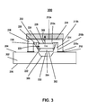
- FIG. 3 is a block diagram of an example of a chip-scale package assembly having a substrate with relief, in accordance with certain configurations of the present disclosure.
- FIG. 4 is a block diagram depicting an example of pin-out of a chip-scale package assembly, in accordance with certain configurations of the present disclosure.
- FIG. 5 is a block diagram of an example of a mixed-mode chip assembly having one die in a flip-chip configuration and another die in a chip-scale package, in accordance with certain configurations of the present disclosure.
- FIG. 6 is a flow chart illustrating exemplary operations of a process of packaging a semiconductor die, in accordance with certain configurations of the present disclosure.
- FIG. 7 is a flow chart illustrating exemplary operations of a process of packaging multiple semiconductor dies, in accordance with certain configurations of the present disclosure.
- the present disclosure provides a multi-chip package method to meet the increased performance requirements (e.g., higher clock speeds and integration of more functions in the same semiconductor package) due to the need to perform high-speed digital communication.
- an OC-768 compliant optical transceiver may require transmission/reception of data traffic at 38,486.016 Mbit/s.
- a microelectronics implementation of such a transceiver may comprise silicon germanium (SiGe) for circuit integration and speed (e.g., data processing functions) and indium phosphide (InP) or gallium arsenide (GaAs) for high voltage swing and speed (e.g., output line driver).
- the present disclosure provides configurations for packaging such dies in a single chip assembly (“mixed-mode packaging”).
- the mixed-mode packaging may be configured to share a same heat sink.
- the present disclosure provides a chip-scale package assembly wherein a die may be coupled to a first surface of a chip-scale frame in a well region and the chip-scale frame is coupled to a second substrate, thereby positioning the die in a space formed by the well region and the second substrate.
- the chip-scale frame may be a well-understood, inexpensive substrate. This choice of the chip-scale frame may facilitate easy testing and yielding of the chip-scale package.
- a lid may be positioned over the die to form a substantially airtight chamber (hermitically sealed) enclosing the die.
- such configurations may protect the die from exposure to gases emitted by adhesives (e.g., hydrogen emission by epoxy adhesive) used in the chip assembly.
- adhesives e.g., hydrogen emission by epoxy adhesive
- the hermitic sealing of the die may make it possible to use inexpensive adhesives for a chip assembly containing a chip-scale package.
- the present disclosure provides a mixed-mode configuration, comprising a flip-chip die configuration and a chip-scale package, both positioned to use a common heat sink.
- the mixed-mode configuration may provide sufficient environmental isolation for the die in the chip-scale package to forego expensive multi-chip hermetic sealing,
- chip-scale package configurations of the present disclosure may allow dense placement of external connectors, such as ball grid array connectors.
- chip-scale package configurations of the present disclosure may lend themselves to a more predictable circuit behavior because unlike a flip-chip configuration in which the integrated circuits on a die are in close proximity to an underfill material with possibly unknown, not-well-controlled, or undesirable electrical characteristics, the integrated circuits on a die in a chip-scale package may be in contact with air or another non-reacting gas, having well-known, well-controlled, and desirable electrical characteristics and composition.
- various configurations described in the present disclosure may be implemented on a silicon, silicon-germanium (SiGe), gallium arsenide (GaAs), indium phosphide (InP) or indium gallium phosphide (InGaP) or any other suitable semiconductor material.
- SiGe silicon-germanium
- GaAs gallium arsenide
- InP indium phosphide
- InGaP indium gallium phosphide
- FIG. 1 is a block diagram depicting a chip assembly 100 having a flip-chip package configuration in accordance with certain configurations of the present disclosure.
- a semiconductor die 102 may be coupled to a substrate 104 having a top surface 118 and a bottom surface 116 , via a coupling mechanism 106 .
- the semiconductor die 102 has a circuit surface 108 , where integrated circuits are located, and a connecting surface 110 , for adhering the die 102 to another component.
- the coupling mechanism 106 may include, for example, (i) solder joints 106 b for electrically coupling electrical contacts 106 a of the die 102 to electrical contacts 106 c of the substrate 104 and (ii) a material known as “underfill” 106 d for filling the space between the solder joints 106 b .
- the coupling mechanism 106 may bond the circuit surface 108 to the top surface 118 of the substrate 104 .
- the connecting surface 110 of the die 102 may be coupled to a substantially planar heat sink 112 , using, for example, an adhesive layer 134 comprising a well-known adhesive material such as epoxy.
- the adhesive material may include a heat transferring material to provide good heat dissipation from the die 102 through the heat sink 112 .
- the heat generated by the integrated circuits 103 located at surface 108 generally may travel upwards, in the direction of arrow 120 , and may be dissipated by the heat sink 112 .
- the bottom surface 116 may have electrical contacts 193 that are coupled to external connectors, such as ball grid array connectors 114 a , to carry electrical signals to/from the die 102 via interconnects 192 in the substrate 104 .
- a flip-chip configuration may be useful for a die comprising a relatively sturdy material such as SiGe or another Si-based material; however, a flip-chip configuration is less desirable, due to durability concerns, for a relatively brittle material such as InP, GaAs, or another III-V semiconductor compound.
- a III-V semiconductor compound may include one or more materials from group III of the periodic table B, Al, Ga, In, Ti) and one or more materials from group V of the periodic table (e.g., P, As, Sb,
- a chip assembly includes a die in the flip-chip configuration and another die not in the flip-chip configuration, the two dies do not conduct heat in the same direction. Therefore, it may not be possible to use a common substantially planar heat sink.
- FIG. 2 is a block diagram of a chip-scale package assembly, in accordance with certain configurations of the present disclosure.
- a chip-scale package assembly 200 may comprise a substrate 202 having a top surface 204 and a bottom surface 206 .
- the top surface 204 and the bottom surface 206 may be planar and may be substantially parallel to each other.
- the substrate 202 may be positioned so that during operation of the chip-scale package assembly 200 , the top surface 204 and the bottom surface 206 are substantially horizontal.
- a chip-scale frame 208 may be positioned on top of the substrate 202 .
- the top surface 204 of the substrate 202 may include contacts 291 for electrically coupling with the chip-scale frame 208 , and the bottom surface 206 may also include contacts 293 for electrically coupling to connectors such as ball grid array connectors 114 b .
- the substrate 202 may include conductive paths such as interconnects 292 between the contacts 291 and the contacts 293 .
- the chip-scale frame 208 may have a generally box-like, rectangular shape.
- the chip-scale frame 208 may have an inside surface 210 (including, for example, 210 a , 210 h and 210 c ) and an outside surface 212 (including, for example, 212 a and 212 b ).
- the inside surface 210 a , 210 b , 210 c and the outside surface 212 a , 212 b may be planar and substantially parallel to each other.
- the inside surface 210 a is parallel to the outside surface 212 a (or the middle portion 212 m of the outside surface 212 a ), the inside surface 210 b is parallel to the outside surface 212 b , and the inside surface 210 c is parallel to the outside surface 212 a (or the outer portion 212 n of the outside surface 212 a ).
- the inside surface 210 of the chip-scale frame may provide a well region 214 with an opening 216 .
- the opening 216 may be rectangular or square in shape
- the well region 214 may be shaped like a rectangular prism with four walls (not shown) forming four sides of the well region 214 .
- other shapes of the opening 216 and the well region 214 are possible.
- the inside surface 210 c may be coupled to the substrate 202 using a coupling mechanism 218 that includes, for example, soldering materials.
- the inside surface 210 c may include electrical contacts 295
- the portion of the substrate 202 , which mates with the inside surface 210 c may also include electrical contacts 291 .
- the coupling mechanism 218 may include (i) solder bumps 218 a for electrically coupling the electrical contacts 295 on the inside surface 210 c to the electrical contacts 291 on the substrate 202 and (ii) an underfill 218 b for filling the gaps between the solder bumps.
- the solder bumps may be used for electrical and/or mechanical coupling, and the underfill may be used for mechanical attachment of the chip-scale frame 208 to the substrate 202 .
- the use of underfill is optional (e.g., not a required element of the attachment method; for example, underfill is not required for a chip-scale packaging (CSP) attachment).
- CSP chip-scale packaging
- a die 220 having a circuit surface 222 and a connecting surface 224 may be housed in the well region 214 by coupling to a wall 226 (e.g., coupling to the bottom surface of the well region 214 , as depicted in FIG. 2 ) of the chip-scale frame 208 using a coupling mechanism 228 .
- the circuit surface 222 and the connecting surface 224 may both be generally planar and parallel to each other.
- the circuit surface 222 and the connecting surface 224 may be on opposite surfaces of the die 220 and face opposite directions (e.g., the circuit surface 222 facing the substrate 202 , and the connecting surface facing a heat sink 232 ).
- the circuit surface 222 may comprise microelectronics (electronic circuits) 203 implemented on the die 220 .
- the die 220 may be coupled to any surface of the well region 214 , but advantageously may be coupled to the bottom (wall 226 ) of the well region 214 , so that during operation, the circuit surface 222 is in a substantially horizontal position. Such positioning of the circuit surface 222 may advantageously help transfer of heat through the die 220 to the heat sink 232 via the chip-scale frame 208 .
- a heat sink may be made of a metal or a highly thermally conductive material.
- the die 220 may be positioned inside the well region 214 leaving a gap 230 between the circuit surface 222 of the die 220 and the top surface 204 of the substrate 202 .
- the gap 230 may be filled by a sealing material (not shown in FIG. 2 ).
- the sealing material may protect microelectronics on the circuit surface 222 as well as be of known electrical characteristics to ensure predictable operation of the microelectronics on the circuit surface 222 .
- the size of the die 220 may be selected to be smaller than the size of the well bottom (wall 226 ) to leave sufficient space to allow placement of connectors (e.g., wire bonds) as further described below.
- both the die 220 and the wall 226 may be shaped similarly having edges parallel to each other (e.g., both rectangular or both square).
- heat generated by microelectronics on the circuit surface 222 may travel through the chip-scale frame 208 towards the outside surface 212 a .
- a heat sink 232 may be coupled to the outside surface 212 a of the chip-scale frame 208 to allow dissipation of heat generated by operation of the integrated circuits on the die 220 .
- the heat sink 232 may be coupled to the outside surface 212 a using an adhesive (e.g., epoxy). In one aspect, it may be advantageous to use a heat-conducting adhesive.
- an adhesive including one or more metals such as a silver-filled adhesive may be provided to adhere the heat sink 232 to the outside surface 212 a and withstand differential thermal expansion between the heat sink 232 and the chip-scale frame 208 .
- an adhesive including one or more metals such as copper or aluminum may be provided to adhere the heat sink 232 to the outside surface 212 a and withstand differential thermal expansion between the heat sink 232 and the chip-scale frame 208 .
- solder bonding may be used to attach the heat sink 232 to the outside surface 212 a enabling a higher thermal conductivity than may be achieved by typical adhesives.
- one or more openings may be provided in the chip-scale frame 208 to allow access from outside.
- the opening(s) may be used to fill the well region 214 with a non-reacting gas or material, or may be used to create vacuum in the well region 214 .
- the coupling mechanism 228 may include two mechanisms: (i) a first coupling mechanism for physically securing the die 220 to the chip-scale frame 208 and (ii) a second coupling mechanism for providing electrical coupling between the contacts 297 on the die 220 and the contacts 294 on the chip-scale frame 208 .
- the die 220 may be secured to the chip-scale frame 208 using an adhesive (e.g., epoxy).
- an adhesive e.g., epoxy
- it may be advantageous to use a thermally-conductive adhesive e.g., an adhesive including one or more metals such as copper, aluminum, tin etc.
- the die 220 may be glued directly onto the chip-scale frame 208 using an epoxy adhesive.
- solder bonding may be used to attach the die 220 to the chip-scale frame 208 .
- the connecting surface 224 is attached to the wall 226 .
- a surface of the die 220 e.g., 224 or another surface
- the second coupling mechanism may include wire bonds 236 for coupling the electrical contacts 297 on the circuit surface 222 with the electrical contacts 294 on the wall 226 (e.g., wire-bonding 236 ).
- the circuit surface 222 faces the substrate 202 .
- conductive paths such as interconnects or wiring 290 may be provided in the chip-scale frame 208 between the electrical contacts 294 on the wall 226 and the electrical contacts 295 on the inside surface 210 c.
- wire bonds are more flexible (e.g., more pliable, bendable, deformable, compliant, resilient, yielding) than solder bumps, and for certain configurations (e.g., for dies that are relative brittle), it may be more advantageous to utilize wire bonds between a die and a chip-scale frame.
- electrical signals from the die 220 may travel from the die 220 to the connectors 114 b of a chip-scale package assembly via, for example, contacts 297 on the die 220 , wire bonds 236 , contacts 294 on the wall 226 of the chip-scale frame 208 , conductive paths 290 , contacts 295 on the inside surface 210 c , the coupling mechanism 218 solder bumps 218 a ), contacts 291 on the top surface 204 , conductive paths 292 , contacts 293 on the bottom surface 206 , and ball grid array connectors 114 b . Electrical signals from the connectors 114 b to the die 220 may travel the same or similar paths in reverse direction.
- the die 220 may comprise InP or GaAs semiconductor material.
- the substrate 202 may comprise layers of high temperature co-fired ceramic (HTCC) material.
- the chip-scale frame 208 may comprise a material such as a ceramic material, bismaleimide triazine (BT), an organic laminate, HTCC, low temperature co-fired ceramic (LTCC), or another suitable substrate material.
- the substrate 202 and the chip-scale frame 208 may both be made of the same material, thereby improving operational performance and durability by having a material with the same coefficient of thermal expansion on both sides of the coupling mechanism 218 .
- a coupling mechanism between a die and a chip-scale frame may include (i) solder bumps (e.g., controlled collapse chip connectors (C4)) for electrically coupling the electrical contacts of the die to the electrical contacts of the chip-scale frame and (ii) an underfill for filling the gaps between the solder bumps.
- solder bumps e.g., controlled collapse chip connectors (C4)
- C4 controlled collapse chip connectors
- an underfill for filling the gaps between the solder bumps.
- a circuit surface of the die that has the electrical contacts of the die
- a contact surface e.g., wall 226 in FIG. 2
- the circuit surface of the die may be physically attached to the contact surface of the chip-scale frame using the solder bumps and underfill; and the electrical contacts on the circuit surface of the die may be electrically coupled to the electrical contacts of the chip-scale frame using the solder bumps.
- a connecting surface of the die may be the same as the circuit surface of the die.
- FIG. 3 is a block diagram of a chip-scale package assembly having a substrate with a relief and a lid, in accordance with certain configurations of the present disclosure.
- a lid 302 may be attached to the chip-scale frame 208 at the wall 226 .
- the lid 302 may be positioned in the gap 230 in the well region 214 to form an airtight (hermitically sealed) chamber 304 around the die 220 .
- the lid 302 may comprise a surface that is substantially flat and parallel to the circuit surface 222 .
- the lid 302 may comprise, for example, ceramic such as alumina, metal such as Kovar, or liquid crystal polymer (LCP).
- a relief 306 may be provided in the substrate 202 .
- white FIG. 3 depicts both a relief 306 and a lid 302 , these features may be provided independently of each other and be present either alone or together in various configurations.
- the relief 306 may be provided to accommodate the lid 302 that would have otherwise been obstructed by the top surface 204 of the substrate 202 .
- heat produced by the die 220 may be dissipated in the direction 308 by the heat sink 232 .
- the relief 306 may be fabricated by removing portions of layers of the substrate 202 during the fabrication process.
- FIG. 4 is a block diagram depicting exemplary pin-out of a die of a chip-scale package assembly, as seen from a substrate side, in accordance with certain configurations of the present disclosure.
- the illustrated configuration shows the contacts 297 of the die 220 in the well region 214 bonded out, using connectors 402 (e.g., wire bonds 236 ), to a plurality of contacts 294 such as connecting pads 404 on the chip-package frame 208 .
- the connecting pads 404 may be metal pads.
- the connecting pads 404 may in turn be electrically coupled to the contacts/connectors (e.g., 291 , 293 , 114 b ) on the substrate 202 , making them available for connection to external electronics.
- the connectors 402 may be appropriately chosen to minimize mechanical abrasion of/stress on the die 220 during the attachment of the connectors 402 and thermal stress during the operation of the die 220 .
- the chip-scale packaging may achieve a “flip-chip” configuration for a die comprising a brittle material such as InP or GaAs, in that, for example, a circuit surface including the circuits or electrical contacts of a die (e.g., 220 ) may face a substrate (e.g., 202 ) without having to adhere a die's circuit surface to the substrate (or to a surface of a rigid component).
- this may allow the use of a known, high yield process to couple the die to a substrate using wire bonding, as needed. Because the die may operate effectively in a “flip-chip” position, the heat generated by the integrated circuits on the die may escape in the upward direction, making it possible to dissipate the heat by placing a heat sink on top of the chip-scale package.
- FIG. 5 is a block diagram of a mixed-mode chip assembly 500 having one die in a flip-chip configuration and another die in a chip-scale package, in accordance with certain configurations of the present disclosure.
- a die 102 in a flip-chip configuration
- die 220 in a chip-scale package
- one or more integrated circuits on die 102 may be coupled to one or more integrated circuits on die 220 (via connectors 250 in the substrate 202 and via connectors in the chip-scale frame 208 ) to pass electrical signals between the die 102 and the die 220 .
- the connectors 250 may comprise electrical interconnects in the substrate 202 .
- the configuration illustrated in FIG. 5 shows two dies, other configurations comprising more than two dies are also possible (e.g., multi-chip modules).
- configurations comprising more than two dies in a mixed-mode assembly one or more dies in a flip-chip configuration and one or more dies in a chip-scale package may be present.
- connectors 250 may or may not be present between each pair of the dies on such a multi-die configuration,
- the dies 102 and 220 may generate heat that may be transferred in the direction of arrows 252 and 254 , respectively.
- the heat sink 232 may be positioned to simultaneously dissipate heat generated by operation of the dies 102 and 220 .
- the heat sink 232 may generally have a fiat plate-like shape with an upper surface 504 facing away from the dies 102 and 220 and a lower surface 506 facing the dies 102 and 220 .
- the outside surface 212 a of the chip-scale frame 208 and the connecting surface 110 of the die 102 are not at the same level, and the lower surface 506 of the heat sink 232 has a step 502 dividing the lower surface 506 in into two substantially planar parts, each part leveled to couple with the respective die (e.g., coupled to the die 102 , or coupled to the die 220 via the chip-scale flame 208 ).
- the lower surface 506 may in general comprise multiple levels to take into account different die/package elevations.
- the multiple levels of the lower surface 506 may be coupled to each other via a joint-shaped-like step (as depicted in FIG. 5 ), a ramp, a rolling joint, or another suitable joint.
- the heat sink 232 may be attached at its lower surface 506 to the outside surface 212 a and the connecting surface 110 using an adhesive material that is a good heat conductor to facilitate heat transfer from the dies 102 and 220 to the heat sink 232 .
- the adhesive material used to adhere the outside surface 212 a . to the heat sink 232 may be different from the adhesive material used to adhere the connecting surface 110 to the heat sink 232 (e.g., different adhesive materials to match the coefficients of thermal expansion of different materials of the outside surface 212 a and the connecting surface 110 ).
- the bottom surface 206 of the substrate 202 may be coupled to ball grid array connectors 114 c to facilitate coupling of the integrated circuits on dies 102 and 220 to outside electronics.
- other well-known connection methods may be employed to conduct electrical signals to/from the dies 102 , 220 utilizing another surface of the substrate 202 (e.g., vertical surface 508 ).
- Such connectors may include, for example, coaxial connectors, GPO or GPPO connectors, solder joints, leadless contacts, or other suitable connectors.
- the die 102 is electrically insulated from the heat sink 232 .
- the connecting surface 110 of the die 102 is electrically coupled to the heat sink 232 , in which case the adhesive layer 134 is electrically conductive.
- the bulk of the die 102 (which may be referred to as the substrate of the die 102 ) may be used for ground or power (e.g., Vcc or Vdd), and the connecting surface 110 may couple the ground or power path of the die 102 to the heat sink 232 .
- a heat sink is thermally conductive.
- a heat sink is thermally and electrically conductive.
- the substrate 202 is an insulator that includes electrically conductive paths (e.g., contacts, interconnects and connectors).
- the chip-scale frame 208 is an insulator that includes electrically conductive paths (e.g., contacts, interconnects and connectors).
- two dies in a chip assembly are made of the same material (e.g., silicon) but from two different processes, and only one of the dies supports a flip-chip bumping process.
- FIG. 6 is a flow chart of an exemplary process for creating a semiconductor package, in accordance with certain configurations of the present disclosure.
- a first die e.g., 220 in FIG. 2 or 3
- the circuit surface may comprise integrated circuits, and the connecting surface may be configured for adhesion to another surface.
- a circuit surface is different from a connecting surface.
- a circuit surface may be on the same surface as a connecting surface.
- the first die may comprise, for example, a semiconductor material such as silicon germanium (SiGe), indium phosphide (InP) or gallium arsenide (GaAs).
- a chip-scale frame (e.g., 208 ), having an inside surface and an outside surface, may be provided.
- the chip-scale frame may have a well region having an opening within the inside surface.
- the chip-scale frame may comprise a material such as HTCC, LTCC, a ceramic material, bismaleimide triazine (BT), or an organic laminate.
- the first die may be coupled to a wall of the well region using a coupling mechanism.
- the coupling mechanism may comprise, for example, attaching the first die to the wall.
- the coupling mechanism may further include coupling the electrical contacts on the circuit surface with contacts on the chip-scale frame.
- the first die may be positioned to have a gap between the circuit surface and a substrate (e.g., 202 ).
- a substrate may be provided for mounting the first die and the chip-scale frame.
- the substrate may have a top surface and a bottom surface.
- the substrate may be made of a material such as HTCC.
- an inside surface of the chip-scale frame may be coupled with the top surface of the substrate by a coupling mechanism.
- This coupling mechanism may include, for example, soldering materials.
- a heat sink e.g., 232
- This coupling mechanism may include, for example, an adhesive material that is a good conductor of heat to facilitate heat transfer from the first die to the heat sink
- operation 612 may be performed prior to operation 608 or 610 .
- a lid (e.g., 302 ) may be attached to the chip-scale frame, the lid being positioned in a gap between a circuit surface of the first die and the top surface of the substrate, the lid forming a substantially airtight chamber around the first die.
- the airtight chamber may be filled with a non-reacting gas such an inert gas (e.g., xenon), to protect the integrated circuits on the die from exposure to vapors from epoxy material and/or other soldering material used in the chip assembly and from other gaseous emissions from the substrate or other components of a chip-scale package assembly.
- the operation of attaching the lid may be performed prior to operation 608 or prior to coupling the chip-scale package assembly (including 208 and 220 ) to the substrate in operation 610 . It should be noted that some of the operations described with respect to FIG. 6 may be performed in different order or performed simultaneously.
- the process of mixed-mode packaging may include attaching at least two dies to a substrate (see, e.g., FIG. 5 ).
- a first assembly including a first die attached to a chip-scale frame (with or without a lid) may be provided.
- a second die may be provided.
- the first assembly and the second die may be attached to a substrate using a coupling mechanism, including both electrical and mechanical coupling. For example, solder bumps (e.g., 218 a.
- solder bumps e.g., 106 b
- solder bumps e.g., 106 b
- an underfill material may be provided between the first assembly and the substrate and between the second die and the substrate.
- the first assembly and the second die are attached to the substrate simultaneously in one step.
- either the first assembly or the second die is attached to the substrate first, and then the other one is attached to the substrate subsequently.
- a heat sink e.g., 232
- solder bumps may be referred to as solder joints or solder balls.
- the second die may be attached to the substrate in a flip-chip configuration.
- the second die may be electrically coupled to external connectors (e.g., ( 14 c ) of the substrate via interconnects (e.g., 292 ), electrically coupled to the first die via interconnects (e.g., 250 ) embedded in the substrate, and mechanically attached to the heat sink
- the second die may comprise, for example, SiGe material.
- the connectors or interconnects (e.g., 250 ) may be shielded to minimize radiative interference with each other and/or electronic circuitry on the first die and the second die.
- a plurality of connectors such as ball grid array (BGA) connectors (e.g., 114 c ), may be attached to the bottom surface of the substrate (e.g., 202 ) to facilitate connection to external circuits.
- the connectors may be attached to another surface (e.g., on a side of the substrate 202 other than the top surface 204 or the bottom surface 206 of the substrate) and may be of another well-known type (e.g., GPPO connectors).
- the lower surface (e.g., 506 ) of the heat sink (e.g., 232 ) may be suitably leveled to achieve close thermal coupling of the heat sink and the first assembly and close thermal coupling of the heat sink and the second die.
- the mixed-mode packaging described above may also be used to package multiple dies of the same type (or different type in some examples) on a substrate.
- more than one chip-scale package may be packaged together and placed on one substrate in a multi-chip module.
- each chip-scale package may include a chip-scale frame, one or more dies, and optionally a heat sink.
- the chip-scale packages may be connected by connectors embedded in a substrate.
- such mixed-mode packaging may provide operational advantages such as being able to use an inexpensive process to mount a die on a substrate, being able to isolate integrated circuits on a circuit surface from exposure to emissions from chemicals in the package and electromagnetic interference from other circuits or connectors, being able to use the entire bottom surface of the substrate for placing ball grid arrays, and being able to share, among multiple dies, a common heat sink advantageously placed in the direction of heat dissipation.
- a package including one or more semiconductor dies may be hermitically sealed.
- each of the dies may be hermitically sealed individually and separately, or multiple dies may be hermitically sealed together. These dies may be mounted on the same substrate and share the same heat sink. This provides an inexpensive manufacturing process over traditional methods.
- a chip assembly comprising:
- the substrate comprises high temperature co-fired ceramic (HTCC), and wherein the chip-scale frame comprises HTCC, a ceramic material, bismaleimide triazine (BT), or an organic laminate.
- HTCC high temperature co-fired ceramic
- BT bismaleimide triazine
- a method of packaging one or more semiconductor dies comprising:
- the substrate comprises high temperature co-fired ceramic (HTCC) and the chip-scale frame comprises HTCC or a ceramic material or bismaleimide triazine (BT) or an organic laminate.
- HTCC high temperature co-fired ceramic
- BT bismaleimide triazine
- the first die comprises indium phosphide (InP) or gallium arsenide (GaAs).
- connection may refer to being directly connected or coupled.
- connection may refer to being indirectly connected or coupled.
- an integrated circuit may refer to a circuit comprising at least one transistor. In another example, an integrated circuit may refer to a circuit comprising a plurality of transistors. In yet another example, an integrated circuit may refer to a circuit comprising more than a hundred transistors. In one example, an integrated circuit may refer to a circuit comprising one or more bipolar junction transistors, one or more field effect transistors, and/or one or more other components. In one example, a circuit may include one or more of a passive component (e.g., a resistor, a capacitor) and/or an active component (e.g., a transistor).
- a passive component e.g., a resistor, a capacitor
- an active component e.g., a transistor
- a chip-scale package may be a package that includes a die.
- a chip-scale package may include one or more dies, attached to a substrate and wire-bonded.
- a chip-scale package may include a die attached to a substrate using an epoxy material and wire bonds, and may further include a lid covering the die and hermitically sealing the die.
- a chip-scale package may comprise a substrate made of a dielectric material and a chip bonded to the substrate and electrically coupled to the substrate using a well-known method such as wire- bonding.
- wire bonds are not limited to traditional wire bonds (e,g., ball bonds and wedge bonds).
- wire bonds may refer to flexible connectors.
- wire bonds may refer to connectors that are flexible enough so that they do not break away during the manufacturing of a package (e.g., while the die is being attached to its substrate or to its chip-scale frame).
- wire bonds may refer to connectors that are sufficiently flexible so that they do not break away during the normal operation of the package subjected to temperature variance.
- a phrase such as an “aspect” does not imply that such aspect is essential to the subject technology or that such aspect applies to all configurations of the subject technology.
- a disclosure relating to an aspect may apply to all configurations, or one or more configurations.
- An aspect may provide one or more examples.
- a phrase such as an aspect may refer to one or more aspects and vice versa.
- a phrase such as a “configuration” does not imply that such configuration is essential to the subject technology or that such configuration applies to all configurations of the subject technology.
- a disclosure relating to a configuration may apply to all configurations, or one or more configurations.
- a configuration may provide one or more examples.
- a phrase such a configuration may refer to one or more configurations and vice versa.
Abstract
Description
-
- a substrate having a top surface and a bottom surface;
- a first die having a circuit surface and a connecting surface, the circuit surface comprising one or more integrated circuits;
- a chip-scale frame having an inside surface, an outside surface, and a well region, the well region having an opening within the inside surface, the well region having a wall, the well region housing the first die, the first die attached to the wall by a first coupling mechanism, the inside surface coupled to the top surface of the substrate by a second coupling mechanism; and
- a heat sink coupled to the outside surface of the chip-scale frame using a third coupling mechanism.
-
- a second die having a second circuit surface and a second connecting surface, the second circuit surface comprising one or more integrated circuits, contacts on the second circuit surface coupled to contacts on the top surface of the substrate for electrical communication, a circuit on the second die coupled to a circuit on the first die for electrical communication via connectors embedded in the substrate and via connectors embedded in the chip-scale frame, the second connecting surface attached to the heat sink for at least thermal conduction, the second die disposed between the heat sink and the substrate,
- wherein the first die and the chip-scale frame are disposed laterally adjacent to the second die, the first die is disposed between the chip-scale frame and the substrate, the chip-scale frame is disposed between the heat sink and the substrate, the circuit surface faces toward the substrate, the connecting surface faces toward the heat sink, contacts on the circuit surface are coupled to contacts on the wall using wire bonds, and the connecting surface is attached to the wall using an adhesive,
- wherein the second coupling mechanism comprises solder joints for electrical communication, and the third coupling mechanism comprises an adhesive that is at least thermally conductive.
-
- a second die in a flip-chip configuration attached to the substrate and coupled to the first die for electrical communication via connectors embedded in the substrate, the second die further coupled to the heat sink.
-
- a lid attached to the chip-scale frame, the lid being positioned in a gap between the circuit surface of the first die and the top surface of the substrate, the lid forming a substantially airtight chamber around the first die.
-
- providing a first die having a circuit surface and a connecting surface;
- providing a chip-scale frame having an inside surface and an outside surface, the chip-scale frame having a well region having an opening in the inside surface;
- coupling the first die to a wall of the well region using a first coupling mechanism for electrical and mechanical coupling;
- providing a substrate having a top surface and a bottom surface;
- coupling the inside surface of the chip-scale frame with the top surface of the substrate by a second coupling mechanism, wherein a gap is provided between the circuit surface of the first die and the top surface of the substrate; and
- coupling a heat sink to the outside surface of the chip-scale frame using a third coupling mechanism.
-
- providing a second die having a second circuit surface and a second connecting surface, the second circuit surface comprising one or more integrated circuits;
- coupling contacts on the second circuit surface to contacts on the top surface of the substrate for electrical communication;
- coupling the second connecting surface to the heat sink for at least thermal conduction, the second die disposed between the heat sink and the substrate,
- wherein the first die and the chip-scale frame are disposed laterally adjacent to the second die, the first die is disposed between the chip-scale frame and the substrate, the chip-scale frame is disposed between the heat sink and the substrate, the circuit surface faces toward the substrate, the connecting surface faces toward the heat sink, contacts on the circuit surface are coupled to contacts on the wall using wire bonds, and the connecting surface is attached to the wall using an adhesive,
- wherein the second coupling mechanism comprises solder joints for electrical communication, the third coupling mechanism comprises an adhesive that is at least thermally conductive, and a circuit on the second die is coupled to a circuit on the first die for electrical communication via connectors embedded in the substrate and via connectors embedded in the chip-scale frame.
-
- attaching a second die in a flip-chip configuration to the substrate, wherein the second die is coupled to the first die for electrical communication via connectors embedded in the substrate and via connectors embedded in the chip-scale frame; and
- coupling the second die to the heat sink.
-
- attaching a lid to the chip-scale frame, the lid being positioned in a gap between the circuit surface of the first die and the top surface of the substrate, the lid forming a substantially airtight chamber around the first die.
Claims (6)
Priority Applications (1)
| Application Number | Priority Date | Filing Date | Title |
|---|---|---|---|
| US13/742,252 US8703540B2 (en) | 2009-12-10 | 2013-01-15 | Chip-scale semiconductor die packaging method |
Applications Claiming Priority (3)
| Application Number | Priority Date | Filing Date | Title |
|---|---|---|---|
| US12/635,677 US8093714B2 (en) | 2009-12-10 | 2009-12-10 | Chip assembly with chip-scale packaging |
| US13/347,543 US8367469B2 (en) | 2009-12-10 | 2012-01-10 | Chip-scale semiconductor die packaging method |
| US13/742,252 US8703540B2 (en) | 2009-12-10 | 2013-01-15 | Chip-scale semiconductor die packaging method |
Related Parent Applications (1)
| Application Number | Title | Priority Date | Filing Date |
|---|---|---|---|
| US13/347,543 Continuation US8367469B2 (en) | 2009-12-10 | 2012-01-10 | Chip-scale semiconductor die packaging method |
Publications (2)
| Publication Number | Publication Date |
|---|---|
| US20130130441A1 US20130130441A1 (en) | 2013-05-23 |
| US8703540B2 true US8703540B2 (en) | 2014-04-22 |
Family
ID=44141992
Family Applications (3)
| Application Number | Title | Priority Date | Filing Date |
|---|---|---|---|
| US12/635,677 Expired - Fee Related US8093714B2 (en) | 2009-12-10 | 2009-12-10 | Chip assembly with chip-scale packaging |
| US13/347,543 Active US8367469B2 (en) | 2009-12-10 | 2012-01-10 | Chip-scale semiconductor die packaging method |
| US13/742,252 Expired - Fee Related US8703540B2 (en) | 2009-12-10 | 2013-01-15 | Chip-scale semiconductor die packaging method |
Family Applications Before (2)
| Application Number | Title | Priority Date | Filing Date |
|---|---|---|---|
| US12/635,677 Expired - Fee Related US8093714B2 (en) | 2009-12-10 | 2009-12-10 | Chip assembly with chip-scale packaging |
| US13/347,543 Active US8367469B2 (en) | 2009-12-10 | 2012-01-10 | Chip-scale semiconductor die packaging method |
Country Status (3)
| Country | Link |
|---|---|
| US (3) | US8093714B2 (en) |
| EP (1) | EP2510544A4 (en) |
| WO (1) | WO2011071780A1 (en) |
Families Citing this family (21)
| Publication number | Priority date | Publication date | Assignee | Title |
|---|---|---|---|---|
| US8093714B2 (en) | 2009-12-10 | 2012-01-10 | Semtech Corporation | Chip assembly with chip-scale packaging |
| TWI405279B (en) * | 2010-07-23 | 2013-08-11 | Global Unichip Corp | Packaging of semiconductor components |
| US8637981B2 (en) * | 2011-03-30 | 2014-01-28 | International Rectifier Corporation | Dual compartment semiconductor package with temperature sensor |
| US9006889B2 (en) | 2011-11-11 | 2015-04-14 | Skyworks Solutions, Inc. | Flip chip packages with improved thermal performance |
| US9312817B2 (en) | 2012-07-20 | 2016-04-12 | Freescale Semiconductor, Inc. | Semiconductor package design providing reduced electromagnetic coupling between circuit components |
| EP2750182A1 (en) * | 2012-12-28 | 2014-07-02 | Services Pétroliers Schlumberger | Electronic device sealing for a downhole tool |
| JP6056490B2 (en) * | 2013-01-15 | 2017-01-11 | 株式会社ソシオネクスト | Semiconductor device and manufacturing method thereof |
| CN203377255U (en) * | 2013-06-27 | 2014-01-01 | 比亚迪股份有限公司 | LED radiating bracket |
| US9240390B2 (en) * | 2013-06-27 | 2016-01-19 | Freescale Semiconductor, Inc. | Semiconductor packages having wire bond wall to reduce coupling |
| US9269700B2 (en) | 2014-03-31 | 2016-02-23 | Micron Technology, Inc. | Stacked semiconductor die assemblies with improved thermal performance and associated systems and methods |
| JP2016115727A (en) * | 2014-12-11 | 2016-06-23 | 株式会社東芝 | Semiconductor device |
| US9472484B2 (en) * | 2015-02-17 | 2016-10-18 | Avago Technologies General Ip (Singapore) Pte. Ltd. | Semiconductor structure having thermal backside core |
| US10199356B2 (en) | 2017-02-24 | 2019-02-05 | Micron Technology, Inc. | Semiconductor device assembles with electrically functional heat transfer structures |
| US10861803B1 (en) * | 2017-03-17 | 2020-12-08 | Scientific Components Corporation | Low cost millimeter wave integrated LTCC package and method of manufacturing |
| US10090282B1 (en) * | 2017-06-13 | 2018-10-02 | Micron Technology, Inc. | Semiconductor device assemblies with lids including circuit elements |
| JP6652144B2 (en) * | 2018-01-25 | 2020-02-19 | 日本電気株式会社 | Electronic parts, manufacturing method of electronic parts, mechanical parts |
| CN109411370B (en) * | 2018-09-20 | 2020-09-18 | 西安空间无线电技术研究所 | HTCC system-level packaging structure and packaging method of flip chip |
| CN109920766B (en) * | 2019-03-08 | 2020-12-11 | 中国科学院微电子研究所 | Large-size chip system-in-package structure with heat dissipation structure and manufacturing method thereof |
| US11948855B1 (en) | 2019-09-27 | 2024-04-02 | Rockwell Collins, Inc. | Integrated circuit (IC) package with cantilever multi-chip module (MCM) heat spreader |
| US11037853B1 (en) * | 2019-12-17 | 2021-06-15 | Advanced Semiconductor Engineering, Inc. | Semiconductor package structure and method of manufacturing the same |
| CN113066730B (en) * | 2021-03-25 | 2022-06-10 | 深圳市尚鼎芯科技有限公司 | High-current MOSFET packaging process based on microporous silicon ceramic |
Citations (15)
| Publication number | Priority date | Publication date | Assignee | Title |
|---|---|---|---|---|
| US5444296A (en) * | 1993-11-22 | 1995-08-22 | Sun Microsystems, Inc. | Ball grid array packages for high speed applications |
| US5900675A (en) | 1997-04-21 | 1999-05-04 | International Business Machines Corporation | Organic controlled collapse chip connector (C4) ball grid array (BGA) chip carrier with dual thermal expansion rates |
| US5940271A (en) | 1997-05-02 | 1999-08-17 | Lsi Logic Corporation | Stiffener with integrated heat sink attachment |
| US6072700A (en) * | 1997-06-30 | 2000-06-06 | Hyundai Electronics Industries Co., Ltd. | Ball grid array package |
| US6340842B1 (en) | 1998-04-02 | 2002-01-22 | Oki Electric Industry Co., Ltd. | Semiconductor device in a recess of a semiconductor plate |
| US20020036541A1 (en) | 2000-09-22 | 2002-03-28 | Buer Kenneth V. | Mmic folded power amplifier |
| US20020043658A1 (en) | 1999-08-30 | 2002-04-18 | Mess Leonard E. | Apparatus and methods of packaging and testing die |
| US20070117270A1 (en) | 2005-03-30 | 2007-05-24 | Renavikar Mukul P | Integrated heat spreader with intermetallic layer and method for making |
| US7271028B1 (en) | 1999-12-15 | 2007-09-18 | Benedict G Pace | High density electronic interconnection |
| US20080179758A1 (en) | 2007-01-25 | 2008-07-31 | Raytheon Company | Stacked integrated circuit assembly |
| US20080258278A1 (en) | 2002-04-29 | 2008-10-23 | Mary Jean Ramos | Partially patterned lead frames and methods of making and using the same in semiconductor packaging |
| CN101303983A (en) | 2007-05-11 | 2008-11-12 | 矽品精密工业股份有限公司 | Heat radiation type semiconductor encapsulation structure and manufacturing method thereof |
| US20090115048A1 (en) | 2004-06-21 | 2009-05-07 | Broadcom Corporation | Multipiece Apparatus for Thermal and Electromagnetic Interference (EMI) Shielding Enhancement in Die-Up Array Packages and Method of Making the Same |
| US20090244812A1 (en) * | 2008-04-01 | 2009-10-01 | Avx Corporation | Hermetically Sealed Capacitor Assembly |
| WO2011071780A1 (en) | 2009-12-10 | 2011-06-16 | Semtech Corporation | Chip assembly with chip-scale packaging |
Family Cites Families (2)
| Publication number | Priority date | Publication date | Assignee | Title |
|---|---|---|---|---|
| US20020079572A1 (en) * | 2000-12-22 | 2002-06-27 | Khan Reza-Ur Rahman | Enhanced die-up ball grid array and method for making the same |
| TW571406B (en) * | 2002-08-23 | 2004-01-11 | Via Tech Inc | High performance thermally enhanced package and method of fabricating the same |
-
2009
- 2009-12-10 US US12/635,677 patent/US8093714B2/en not_active Expired - Fee Related
-
2010
- 2010-12-03 WO PCT/US2010/058965 patent/WO2011071780A1/en active Application Filing
- 2010-12-03 EP EP10836458.9A patent/EP2510544A4/en not_active Ceased
-
2012
- 2012-01-10 US US13/347,543 patent/US8367469B2/en active Active
-
2013
- 2013-01-15 US US13/742,252 patent/US8703540B2/en not_active Expired - Fee Related
Patent Citations (15)
| Publication number | Priority date | Publication date | Assignee | Title |
|---|---|---|---|---|
| US5444296A (en) * | 1993-11-22 | 1995-08-22 | Sun Microsystems, Inc. | Ball grid array packages for high speed applications |
| US5900675A (en) | 1997-04-21 | 1999-05-04 | International Business Machines Corporation | Organic controlled collapse chip connector (C4) ball grid array (BGA) chip carrier with dual thermal expansion rates |
| US5940271A (en) | 1997-05-02 | 1999-08-17 | Lsi Logic Corporation | Stiffener with integrated heat sink attachment |
| US6072700A (en) * | 1997-06-30 | 2000-06-06 | Hyundai Electronics Industries Co., Ltd. | Ball grid array package |
| US6340842B1 (en) | 1998-04-02 | 2002-01-22 | Oki Electric Industry Co., Ltd. | Semiconductor device in a recess of a semiconductor plate |
| US20020043658A1 (en) | 1999-08-30 | 2002-04-18 | Mess Leonard E. | Apparatus and methods of packaging and testing die |
| US7271028B1 (en) | 1999-12-15 | 2007-09-18 | Benedict G Pace | High density electronic interconnection |
| US20020036541A1 (en) | 2000-09-22 | 2002-03-28 | Buer Kenneth V. | Mmic folded power amplifier |
| US20080258278A1 (en) | 2002-04-29 | 2008-10-23 | Mary Jean Ramos | Partially patterned lead frames and methods of making and using the same in semiconductor packaging |
| US20090115048A1 (en) | 2004-06-21 | 2009-05-07 | Broadcom Corporation | Multipiece Apparatus for Thermal and Electromagnetic Interference (EMI) Shielding Enhancement in Die-Up Array Packages and Method of Making the Same |
| US20070117270A1 (en) | 2005-03-30 | 2007-05-24 | Renavikar Mukul P | Integrated heat spreader with intermetallic layer and method for making |
| US20080179758A1 (en) | 2007-01-25 | 2008-07-31 | Raytheon Company | Stacked integrated circuit assembly |
| CN101303983A (en) | 2007-05-11 | 2008-11-12 | 矽品精密工业股份有限公司 | Heat radiation type semiconductor encapsulation structure and manufacturing method thereof |
| US20090244812A1 (en) * | 2008-04-01 | 2009-10-01 | Avx Corporation | Hermetically Sealed Capacitor Assembly |
| WO2011071780A1 (en) | 2009-12-10 | 2011-06-16 | Semtech Corporation | Chip assembly with chip-scale packaging |
Also Published As
| Publication number | Publication date |
|---|---|
| US20130130441A1 (en) | 2013-05-23 |
| EP2510544A4 (en) | 2014-01-22 |
| US8093714B2 (en) | 2012-01-10 |
| US20110140260A1 (en) | 2011-06-16 |
| EP2510544A1 (en) | 2012-10-17 |
| US8367469B2 (en) | 2013-02-05 |
| US20120115279A1 (en) | 2012-05-10 |
| WO2011071780A1 (en) | 2011-06-16 |
Similar Documents
| Publication | Publication Date | Title |
|---|---|---|
| US8703540B2 (en) | Chip-scale semiconductor die packaging method | |
| US7445955B2 (en) | Multichip module package and fabrication method | |
| US8802475B2 (en) | Method of fabricating a 3D integrated electronic device structure including increased thermal dissipation capabilities | |
| US6951773B2 (en) | Chip packaging structure and manufacturing process thereof | |
| US6084308A (en) | Chip-on-chip integrated circuit package and method for making the same | |
| KR100903063B1 (en) | Low profile ball grid array bga package with exposed die and method of making same | |
| US20090014856A1 (en) | Microbump seal | |
| US7696055B2 (en) | Method for manufacturing passive device and semiconductor package using thin metal piece | |
| US20020044423A1 (en) | Method and apparatus for mounting and packaging electronic components | |
| JP2008533700A (en) | Nested integrated circuit package on package system | |
| TW200901433A (en) | Stackable package by using internal stacking modules | |
| TWI785515B (en) | Semiconductor packages and apparatus having the same | |
| KR20150116844A (en) | Package-on-package structures | |
| US20030034557A1 (en) | Chip carrier for a semiconductor chip module | |
| WO2021195942A1 (en) | Photoelectric co-packaging integrated device | |
| JPH0677361A (en) | Multi-chip module | |
| US20040212097A1 (en) | Flip chip package | |
| JPH0744243B2 (en) | Semiconductor integrated circuit module | |
| US11869858B2 (en) | Packaging high-frequency microwave circuits using hot via die attach with interposer | |
| Yu et al. | Integrated Circuit Package Types | |
| JP3267671B2 (en) | Semiconductor device | |
| JPH09275169A (en) | Semiconductor device mounting structure | |
| KR20010094494A (en) | Silicon chip package and method for fabricating silicon chip package | |
| JPH0722575A (en) | Semiconductor device | |
| JPH05251599A (en) | Semiconductor chip module and its manufacture |
Legal Events
| Date | Code | Title | Description |
|---|---|---|---|
| AS | Assignment |
Owner name: HSBC BANK USA, NATIONAL ASSOCIATION, CALIFORNIA Free format text: SECURITY INTEREST;ASSIGNOR:SEMTECH CORPORATION;REEL/FRAME:035732/0347 Effective date: 20150513 |
|
| AS | Assignment |
Owner name: HSBC BANK USA, NATIONAL ASSOCIATION, AS ADMINISTRATIVE AGENT, CALIFORNIA Free format text: SECURITY INTEREST;ASSIGNORS:SEMTECH CORPORATION;SEMTECH NEW YORK CORPORATION;SIERRA MONOLITHICS, INC.;AND OTHERS;SIGNING DATES FROM 20151115 TO 20161115;REEL/FRAME:040646/0799 Owner name: HSBC BANK USA, NATIONAL ASSOCIATION, AS ADMINISTRA Free format text: SECURITY INTEREST;ASSIGNORS:SEMTECH CORPORATION;SEMTECH NEW YORK CORPORATION;SIERRA MONOLITHICS, INC.;AND OTHERS;SIGNING DATES FROM 20151115 TO 20161115;REEL/FRAME:040646/0799 |
|
| FEPP | Fee payment procedure |
Free format text: MAINTENANCE FEE REMINDER MAILED (ORIGINAL EVENT CODE: REM.) |
|
| LAPS | Lapse for failure to pay maintenance fees |
Free format text: PATENT EXPIRED FOR FAILURE TO PAY MAINTENANCE FEES (ORIGINAL EVENT CODE: EXP.) |
|
| STCH | Information on status: patent discontinuation |
Free format text: PATENT EXPIRED DUE TO NONPAYMENT OF MAINTENANCE FEES UNDER 37 CFR 1.362 |
|
| FP | Lapsed due to failure to pay maintenance fee |
Effective date: 20180422 |
|
| AS | Assignment |
Owner name: JPMORGAN CHASE BANK, N.A., AS SUCCESSOR AGENT, ILLINOIS Free format text: ASSIGNMENT OF PATENT SECURITY INTEREST PREVIOUSLY RECORDED AT REEL/FRAME (040646/0799);ASSIGNOR:HSBC BANK USA, NATIONAL ASSOCIATION, AS RESIGNING AGENT;REEL/FRAME:062781/0544 Effective date: 20230210 |