US8680534B2 - Vertical light emitting diodes (LED) having metal substrate and spin coated phosphor layer for producing white light - Google Patents
Vertical light emitting diodes (LED) having metal substrate and spin coated phosphor layer for producing white light Download PDFInfo
- Publication number
- US8680534B2 US8680534B2 US13/227,335 US201113227335A US8680534B2 US 8680534 B2 US8680534 B2 US 8680534B2 US 201113227335 A US201113227335 A US 201113227335A US 8680534 B2 US8680534 B2 US 8680534B2
- Authority
- US
- United States
- Prior art keywords
- led
- layer
- light
- phosphor layer
- spin coated
- Prior art date
- Legal status (The legal status is an assumption and is not a legal conclusion. Google has not performed a legal analysis and makes no representation as to the accuracy of the status listed.)
- Active
Links
Images


Classifications
-
- H—ELECTRICITY
- H01—ELECTRIC ELEMENTS
- H01L—SEMICONDUCTOR DEVICES NOT COVERED BY CLASS H10
- H01L33/00—Semiconductor devices with at least one potential-jump barrier or surface barrier specially adapted for light emission; Processes or apparatus specially adapted for the manufacture or treatment thereof or of parts thereof; Details thereof
- H01L33/005—Processes
- H01L33/0093—Wafer bonding; Removal of the growth substrate
-
- H—ELECTRICITY
- H01—ELECTRIC ELEMENTS
- H01L—SEMICONDUCTOR DEVICES NOT COVERED BY CLASS H10
- H01L33/00—Semiconductor devices with at least one potential-jump barrier or surface barrier specially adapted for light emission; Processes or apparatus specially adapted for the manufacture or treatment thereof or of parts thereof; Details thereof
- H01L33/48—Semiconductor devices with at least one potential-jump barrier or surface barrier specially adapted for light emission; Processes or apparatus specially adapted for the manufacture or treatment thereof or of parts thereof; Details thereof characterised by the semiconductor body packages
- H01L33/50—Wavelength conversion elements
- H01L33/508—Wavelength conversion elements having a non-uniform spatial arrangement or non-uniform concentration, e.g. patterned wavelength conversion layer, wavelength conversion layer with a concentration gradient of the wavelength conversion material
-
- H—ELECTRICITY
- H01—ELECTRIC ELEMENTS
- H01L—SEMICONDUCTOR DEVICES NOT COVERED BY CLASS H10
- H01L2224/00—Indexing scheme for arrangements for connecting or disconnecting semiconductor or solid-state bodies and methods related thereto as covered by H01L24/00
- H01L2224/01—Means for bonding being attached to, or being formed on, the surface to be connected, e.g. chip-to-package, die-attach, "first-level" interconnects; Manufacturing methods related thereto
- H01L2224/42—Wire connectors; Manufacturing methods related thereto
- H01L2224/47—Structure, shape, material or disposition of the wire connectors after the connecting process
- H01L2224/48—Structure, shape, material or disposition of the wire connectors after the connecting process of an individual wire connector
- H01L2224/4805—Shape
- H01L2224/4809—Loop shape
- H01L2224/48091—Arched
-
- H—ELECTRICITY
- H01—ELECTRIC ELEMENTS
- H01L—SEMICONDUCTOR DEVICES NOT COVERED BY CLASS H10
- H01L2224/00—Indexing scheme for arrangements for connecting or disconnecting semiconductor or solid-state bodies and methods related thereto as covered by H01L24/00
- H01L2224/01—Means for bonding being attached to, or being formed on, the surface to be connected, e.g. chip-to-package, die-attach, "first-level" interconnects; Manufacturing methods related thereto
- H01L2224/42—Wire connectors; Manufacturing methods related thereto
- H01L2224/47—Structure, shape, material or disposition of the wire connectors after the connecting process
- H01L2224/48—Structure, shape, material or disposition of the wire connectors after the connecting process of an individual wire connector
- H01L2224/481—Disposition
- H01L2224/48151—Connecting between a semiconductor or solid-state body and an item not being a semiconductor or solid-state body, e.g. chip-to-substrate, chip-to-passive
- H01L2224/48221—Connecting between a semiconductor or solid-state body and an item not being a semiconductor or solid-state body, e.g. chip-to-substrate, chip-to-passive the body and the item being stacked
- H01L2224/48245—Connecting between a semiconductor or solid-state body and an item not being a semiconductor or solid-state body, e.g. chip-to-substrate, chip-to-passive the body and the item being stacked the item being metallic
- H01L2224/48247—Connecting between a semiconductor or solid-state body and an item not being a semiconductor or solid-state body, e.g. chip-to-substrate, chip-to-passive the body and the item being stacked the item being metallic connecting the wire to a bond pad of the item
-
- H—ELECTRICITY
- H01—ELECTRIC ELEMENTS
- H01L—SEMICONDUCTOR DEVICES NOT COVERED BY CLASS H10
- H01L2224/00—Indexing scheme for arrangements for connecting or disconnecting semiconductor or solid-state bodies and methods related thereto as covered by H01L24/00
- H01L2224/01—Means for bonding being attached to, or being formed on, the surface to be connected, e.g. chip-to-package, die-attach, "first-level" interconnects; Manufacturing methods related thereto
- H01L2224/42—Wire connectors; Manufacturing methods related thereto
- H01L2224/47—Structure, shape, material or disposition of the wire connectors after the connecting process
- H01L2224/48—Structure, shape, material or disposition of the wire connectors after the connecting process of an individual wire connector
- H01L2224/481—Disposition
- H01L2224/48151—Connecting between a semiconductor or solid-state body and an item not being a semiconductor or solid-state body, e.g. chip-to-substrate, chip-to-passive
- H01L2224/48221—Connecting between a semiconductor or solid-state body and an item not being a semiconductor or solid-state body, e.g. chip-to-substrate, chip-to-passive the body and the item being stacked
- H01L2224/48245—Connecting between a semiconductor or solid-state body and an item not being a semiconductor or solid-state body, e.g. chip-to-substrate, chip-to-passive the body and the item being stacked the item being metallic
- H01L2224/48257—Connecting between a semiconductor or solid-state body and an item not being a semiconductor or solid-state body, e.g. chip-to-substrate, chip-to-passive the body and the item being stacked the item being metallic connecting the wire to a die pad of the item
-
- H—ELECTRICITY
- H01—ELECTRIC ELEMENTS
- H01L—SEMICONDUCTOR DEVICES NOT COVERED BY CLASS H10
- H01L2224/00—Indexing scheme for arrangements for connecting or disconnecting semiconductor or solid-state bodies and methods related thereto as covered by H01L24/00
- H01L2224/01—Means for bonding being attached to, or being formed on, the surface to be connected, e.g. chip-to-package, die-attach, "first-level" interconnects; Manufacturing methods related thereto
- H01L2224/42—Wire connectors; Manufacturing methods related thereto
- H01L2224/47—Structure, shape, material or disposition of the wire connectors after the connecting process
- H01L2224/48—Structure, shape, material or disposition of the wire connectors after the connecting process of an individual wire connector
- H01L2224/484—Connecting portions
- H01L2224/48463—Connecting portions the connecting portion on the bonding area of the semiconductor or solid-state body being a ball bond
-
- H—ELECTRICITY
- H01—ELECTRIC ELEMENTS
- H01L—SEMICONDUCTOR DEVICES NOT COVERED BY CLASS H10
- H01L2224/00—Indexing scheme for arrangements for connecting or disconnecting semiconductor or solid-state bodies and methods related thereto as covered by H01L24/00
- H01L2224/01—Means for bonding being attached to, or being formed on, the surface to be connected, e.g. chip-to-package, die-attach, "first-level" interconnects; Manufacturing methods related thereto
- H01L2224/42—Wire connectors; Manufacturing methods related thereto
- H01L2224/47—Structure, shape, material or disposition of the wire connectors after the connecting process
- H01L2224/49—Structure, shape, material or disposition of the wire connectors after the connecting process of a plurality of wire connectors
- H01L2224/491—Disposition
- H01L2224/4918—Disposition being disposed on at least two different sides of the body, e.g. dual array
-
- H—ELECTRICITY
- H01—ELECTRIC ELEMENTS
- H01L—SEMICONDUCTOR DEVICES NOT COVERED BY CLASS H10
- H01L2224/00—Indexing scheme for arrangements for connecting or disconnecting semiconductor or solid-state bodies and methods related thereto as covered by H01L24/00
- H01L2224/80—Methods for connecting semiconductor or other solid state bodies using means for bonding being attached to, or being formed on, the surface to be connected
- H01L2224/85—Methods for connecting semiconductor or other solid state bodies using means for bonding being attached to, or being formed on, the surface to be connected using a wire connector
- H01L2224/85909—Post-treatment of the connector or wire bonding area
- H01L2224/8592—Applying permanent coating, e.g. protective coating
-
- H—ELECTRICITY
- H01—ELECTRIC ELEMENTS
- H01L—SEMICONDUCTOR DEVICES NOT COVERED BY CLASS H10
- H01L2924/00—Indexing scheme for arrangements or methods for connecting or disconnecting semiconductor or solid-state bodies as covered by H01L24/00
- H01L2924/15—Details of package parts other than the semiconductor or other solid state devices to be connected
- H01L2924/181—Encapsulation
-
- H—ELECTRICITY
- H01—ELECTRIC ELEMENTS
- H01L—SEMICONDUCTOR DEVICES NOT COVERED BY CLASS H10
- H01L33/00—Semiconductor devices with at least one potential-jump barrier or surface barrier specially adapted for light emission; Processes or apparatus specially adapted for the manufacture or treatment thereof or of parts thereof; Details thereof
- H01L33/02—Semiconductor devices with at least one potential-jump barrier or surface barrier specially adapted for light emission; Processes or apparatus specially adapted for the manufacture or treatment thereof or of parts thereof; Details thereof characterised by the semiconductor bodies
- H01L33/20—Semiconductor devices with at least one potential-jump barrier or surface barrier specially adapted for light emission; Processes or apparatus specially adapted for the manufacture or treatment thereof or of parts thereof; Details thereof characterised by the semiconductor bodies with a particular shape, e.g. curved or truncated substrate
- H01L33/22—Roughened surfaces, e.g. at the interface between epitaxial layers
-
- H—ELECTRICITY
- H01—ELECTRIC ELEMENTS
- H01L—SEMICONDUCTOR DEVICES NOT COVERED BY CLASS H10
- H01L33/00—Semiconductor devices with at least one potential-jump barrier or surface barrier specially adapted for light emission; Processes or apparatus specially adapted for the manufacture or treatment thereof or of parts thereof; Details thereof
- H01L33/44—Semiconductor devices with at least one potential-jump barrier or surface barrier specially adapted for light emission; Processes or apparatus specially adapted for the manufacture or treatment thereof or of parts thereof; Details thereof characterised by the coatings, e.g. passivation layer or anti-reflective coating
-
- H—ELECTRICITY
- H01—ELECTRIC ELEMENTS
- H01L—SEMICONDUCTOR DEVICES NOT COVERED BY CLASS H10
- H01L33/00—Semiconductor devices with at least one potential-jump barrier or surface barrier specially adapted for light emission; Processes or apparatus specially adapted for the manufacture or treatment thereof or of parts thereof; Details thereof
- H01L33/48—Semiconductor devices with at least one potential-jump barrier or surface barrier specially adapted for light emission; Processes or apparatus specially adapted for the manufacture or treatment thereof or of parts thereof; Details thereof characterised by the semiconductor body packages
- H01L33/64—Heat extraction or cooling elements
- H01L33/641—Heat extraction or cooling elements characterized by the materials
Definitions
- Embodiments of the present invention generally relate to light-emitting diodes (LEDs) and methods for fabricating the same.
- LED light emitting diode
- LCD light crystal displays
- making a light source for white light may involve arranging three light emitting components of red (R), green (G), and blue (B) near each other while diffusing and mixing the light emitted by them.
- R red
- G green
- B blue
- white light of the desired tone cannot be generated due to variations in the tone, luminance, and other factors of the light emitting component.
- the LEDs are made of different materials, electric power required for forward biasing differs from one light emitting diode to another, making it necessary to apply different voltages to different light emitting components, which leads to complex drive circuitry.
- the light emitting components are semiconductor light emitting components
- color tone is subject to variation due to differences in temperature characteristics, chronological changes, and operating environment. Unevenness in color may also be caused by failure to uniformly mix the light emitted by the light emitting components.
- LEDs are effective as light emitting devices for generating individual colors, but a satisfactory light source capable of emitting white light by using LEDs has not been obtained so far.
- U.S. Pat. No. 5,998,925 discloses a white light emitting diode having a light emitting component that uses a semiconductor as a light emitting layer and a phosphor, which absorbs part of the light emitted by the light emitting component and emits light of a wavelength different from that of the absorbed light.
- the light emitting layer of the light emitting component is a nitride compound semiconductor, and the phosphor contains garnet fluorescent material activated with cerium—which contains at least one element selected from the group consisting of Y, Lu, Sc, La, Gd, and Sm and at least one element selected from the group consisting of Al, Ga, and In—and is subject to less deterioration of its emission characteristics, even when used with high luminance for a long period of time.
- FIG. 1 shows an LED as disclosed in the '925 patent.
- This LED is a lead-type LED having a mount lead 2 and an inner lead 4 , wherein a light emitting component 8 is installed on a cup 6 of the mount lead 2 , and the cup 6 is filled with a coating resin 14 that contains a specified phosphor to cover the light emitting component 8 and is molded in resin.
- An n-electrode and a p-electrode of the light emitting component 8 are connected to the mount lead 2 and the inner lead 4 , respectively, by means of wires 12 .
- part of the light emitted by the light emitting component (LED chip) 8 (hereinafter referred to as LED light) excites the phosphor contained in the coating resin 14 to generate fluorescent light having a wavelength different from that of LED light, so that the fluorescent light emitted by the phosphor and the LED light that is output without contributing to the excitation of the phosphor are mixed and output.
- the LED also outputs light having a wavelength different from that of the LED light emitted by the light emitting component 8 .
- FIG. 2 shows a chip embodiment as disclosed in the '925 patent.
- the chip-type LED 26 is installed in a recess of a casing 22 , which is filled with a coating material containing a specified phosphor to form a coating 28 .
- the light emitting component 26 is fixed by using an epoxy resin or the like which contains Ag, for example, and an n-electrode and a p-electrode of the light emitting component 26 are connected to metal terminals 20 installed on the casing 22 by means of conductive wires 24 .
- the chip-type LED constituted as described above, similar to the lead-type LED of FIG.
- fluorescent light emitted by the phosphor and LED light that is transmitted without being absorbed by the phosphor are mixed and output, so that the LED outputs light having a wavelength different from that of LED light emitted by the light emitting component 26 .
- This type of conventional LED suffers from a color ring when used for emitting white light, whereby the color of the emitted light is bluer towards the middle and tends toward yellow at the edges near the casing 22 .
- U.S. Pat. No. 6,642,652 discloses a light source that includes a light emitting device—such as a III-nitride LED where Group 3 (III) includes such elements as Al, Ga, and In—covered with a luminescent material structure, such as a single layer or multiple layers of phosphor. Any variations in the thickness of the luminescent material structure are less than or equal to 10% of the average thickness of the luminescent material structure. In some embodiments, the thickness of the luminescent material structure is less than 10% of a cross-sectional dimension of the light emitting device. In some embodiments, the luminescent material structure is the only luminescent material through which light emitted from the light emitting device passes. In some embodiments, the luminescent material structure is between about 15 and about 100 microns thick. The luminescent material structure is selectively deposited on the light emitting device, for example, by stenciling or electrophoretic deposition.
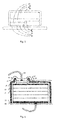
- FIG. 3 An LED coated with phosphor according to the '652 patent is illustrated in FIG. 3 .
- This LED includes an n-type region 44 formed on a substrate 42 , such as sapphire, SiC, or a III-nitride material.
- An active region 46 is formed on the n-type region 44
- a p-type region 36 is formed on the active region 46 .
- the n-type region 44 , the active region 46 , and the p-type region 36 are typically multilayer structures. Portions of the p-type region 36 , the active region 46 , and the n-type region 44 are etched away to expose a portion of n-type region 44 .
- a p-type contact 34 is deposited on the p-type region 36
- an n-type contact 38 is deposited on the exposed portion of the n-type region 44 .
- the LED is then flipped over and mounted to a sub-mount 30 by a material 32 , such as solder.
- the luminescent material structure 40 such as phosphor, is deposited using electrophoresis to surround the LED at the individual die level.
- U.S. Pat. No. 6,744,196 discloses thin film LED devices composed of LED chips that emit light at a first wavelength and a tinted thin film layer over the LED chip that changes the color of the emitted light.
- a blue-light emitting LED chip can be used to produce white light.
- the tinted thin film layer beneficially consists of ZnSe, CeO 2 , Al 2 O 3 , or Y 2 O 3 Ce that is deposited using a chemical vapor deposition (CVD) process, such as metal organic chemical vapor deposition (MOCVD), atomic layer chemical vapor deposition (ALD), plasma enhanced MOCVD, plasma enhanced ALD, and/or photo enhanced CVD. As shown in FIG.
- MOCVD metal organic chemical vapor deposition
- ALD atomic layer chemical vapor deposition
- plasma enhanced MOCVD plasma enhanced ALD
- photo enhanced CVD photo enhanced CVD
- an n-contact 50 is positioned below a reflective layer 52 .
- a tinted layer (a phosphor layer) 53 is positioned above the reflective layer 52 .
- a first passivation layer 54 is formed, and a p-type semi-transparent contact 56 is formed.
- a second passivation layer 58 is formed above the first passivation layer 54 and contact 56 .
- a conductive wire 60 is connected to a p-pad 62 , which is positioned above the p-lead 64 .
- a vertical light emitting diode includes a metal substrate; a p-electrode coupled to the metal substrate; a p-GaN portion coupled to the p-electrode; an active region coupled to the p-GaN portion; an n-GaN portion coupled to the active region; and a phosphor layer coupled to the n-GaN portion.
- Implementations of the above LED can include one or more of the following.
- the metal substrate with a mirror layer is formed on top of the p-GaN portion; using laser lift-off (LLO), selective wet etching, or chemical mechanical polishing, the sapphire carrier is removed.
- the p-contact can also be a light reflector.
- the phosphor layer can be spin-coated or screen printing with a phosphor powder or paste.
- the phosphor layer is patterned using a masking material 101 such as photo resist and dry etched using a fluorine-containing plasma; then a metal layer (e.g., comprising Cr/Ni) is applied to form a contact with n-GaN using various techniques such as PVD, ebeam evaporation, or CVD; the metal bond pad 98 is formed as a contact with n-GaN after the resist 101 is removed and lift-off the unwanted areas of metal 99 to form bond pad 98 . This is called resist lift-off techniques.
- the phosphor layer and the bond pad cover the exposed n-GaN surface 80 .
- the above LED wafer surface with exposed n-GaN portion 80 layer is a substantially smooth, planar surface for subsequent processing.
- the method lowers the cost of producing white LED by coating the phosphor on the blue LEDs at the wafer level directly on top of exposed n-GaN surface, as compared to conventionally coating one LED die at a time.
- the method reduces the amount of phosphor indicated for each die by covering only the exposed n-GaN surface.
- the LEDs do not require wafer bonding or gluing, and the complex and lengthy one-at-a-time wafer bonding/gluing process is replaced by a less complex deposition process such as physical vapor deposition (PVD), chemical vapor deposition (CVD), plasma enhanced CVD (PECVD), evaporation, ion beam deposition, electro chemical deposition, electroless chemical deposition, plasma spray, or ink jet deposition.
- PVD physical vapor deposition
- CVD chemical vapor deposition
- PECVD plasma enhanced CVD
- evaporation ion beam deposition
- electro chemical deposition electroless chemical deposition
- plasma spray or ink jet deposition.
- the metal substrate can dissipate more heat than the sapphire substrate, so more current can be used to drive the LED.
- the resulting LED can replace the conventional LED at a smaller size. For the same LED size, the light output from the vertical LED is significantly higher than the conventional LED for the same drive current.
- FIGS. 1-4 show various prior art light-emitting diodes (LEDs).
- FIG. 5 shows a first embodiment of a vertical LED (VLED) in accordance with one embodiment of the invention.
- FIG. 6 shows the LED of FIG. 5 with a phosphor coating thereon, in accordance with one embodiment of the invention.
- FIG. 7 shows a patterned phosphor coating with a photoresist masking layer, in accordance with one embodiment of the invention.
- FIG. 8 shows a metal contact layer deposited on the patterned phosphor coating of FIG. 7 , in accordance with one embodiment of the invention.
- FIG. 9 shows patterned metal bond pads and a phosphor coating covering the LED wafer, in accordance with one embodiment of the invention.
- FIG. 10 shows a plurality of phosphor-coated LEDs, in accordance with one embodiment of the invention.
- FIG. 5 shows an exemplary structure of one embodiment of a vertical-LED wafer.
- Each LED includes a metal substrate 70 made from a laser lift-off process.
- a p-electrode 72 is positioned above the metal substrate 70 .
- a light reflector and p-contact 74 and a p-GaN portion 76 are positioned above the p-electrode 72 .
- An active region 78 (including a multi-quantum well (MQW)) is formed, and an n-GaN portion 82 is formed above the active region 78 .
- the n-GaN has an exposed surface 80 .
- MQW multi-quantum well
- the LED is formed by depositing a multilayer epitaxial structure above a carrier substrate such as sapphire; depositing at least one metal layer above the multilayer epitaxial structure to form a metal substrate 70 ; and removing the carrier substrate to leave the metal substrate 70 .
- the one or more metal layers can be deposited using electro chemical deposition, electroless chemical deposition, chemical vapor deposition (CVD), metal organic CVD (MOCVD), plasma enhanced CVD (PECVD), atomic layer deposition (ALD), physical vapor deposition (PVD), evaporation, or plasma spray, or any combination of these techniques.
- the metal substrate 70 can be single or multi-layered.
- the one or more metal layers may comprise any of various suitable metals, such as at least one of silver (Ag), aluminum (Al), titanium tungsten (TiW), tungsten (W), molybdenum (Mo), tantalum (Ta), tantalum nitride (TaN), or alloys thereof.
- Ag/Pt or Ag/Pd or Ag/Cr is used as a mirror layer
- nickel (Ni) is used as a barrier for gold (Au) as a seed layer for copper (Cu) plating, which is used as the bulk substrate.
- the mirror layer (comprising Ag, Al, Pt, Ti, or Cr, for example) is deposited, and then a barrier layer comprising any of various suitable materials (such as TiN, TaN, TiWN, TiW with oxygen) is formed above the mirror layer before electro or electroless chemical deposition of a metal, such as Ni or Cu.
- a barrier layer comprising any of various suitable materials (such as TiN, TaN, TiWN, TiW with oxygen) is formed above the mirror layer before electro or electroless chemical deposition of a metal, such as Ni or Cu.
- a seed layer is deposited using CVD, MOCVD, PVD, ALD, or evaporation process; some of the seed materials for copper are tungsten (W), Au, Cu, or Ni, among others.
- the metal layers may have the same or different composition and may be deposited using various deposition techniques.
- the carrier substrate removal can be done using laser, etching, grinding/lapping, chemical mechanical polishing, or wet etching, among others.
- the sapphire substrate can be removed using laser lift-off (LLO) technique.
- the multilayer epitaxial layer can have a reflective metal layer coupled to the metal plating layer.
- a passivation layer 81 is passivating the sidewall of the LED dies and may be coupled to the reflective metal layer (which may function as the p-contact 74 ), p-electrode 72 , p-GaN portion 76 , MQW (e.g., the active region 78 ), and n-GaN portion 82 .
- a p-GaN layer may be coupled to the passivation layer, an n-GaN layer may be coupled to the MQW layer, and an n-electrode may be coupled to the n-GaN layer.
- the metal plating layer may function as a p-electrode or may have a p-electrode coupled thereto.
- FIG. 6 shows phosphor coating 90 on the vertical LED (VLED). Since the LED wafer is substantially smooth and planar, the wafer-level phosphor coating is uniform and parallel to the emitting LED surface 80 . Therefore, color rings do not exist on the LED's field pattern because the blue light emitted from the active layers travels the same distance or light paths through the phosphor layer.
- the LED thickness (GaN layer total thickness is about 2 ⁇ m to 8 ⁇ m) is much smaller than the emitting surface of the n-GaN portion 82 (typically greater than 50 ⁇ m). Light is mainly emitted from the top surface, and a few photons are emitted from the sidewall to minimize issues arising from uneven thickness of the phosphor layer 90 .
- the phosphor layer 90 can be formed using a spin coater.
- the phosphor layer 90 can be coated by the spin-coater spinning between 500 to 30000 rpm to control the layer thickness on the n-side-up vertical-LED wafer.
- other methods such as screen printing, roller method, or dipping method can be used.
- the spin coat method is preferably used.
- the coated film is dried. The drying method is not limited as long as moisture of the film is evaporated. Thus, various methods using a heater, dried air, or surface treatment such as a radiant heat lamp can be used. Alternatively, the coated film may be dried by leaving it in a room temperature environment for a long time.
- a phosphor powder composition is prepared.
- a dispersing agent is dispersed in purified water, and the dispersion is stirred with a homomixer and placed in the purified water in which the dispersing agent has been dispersed, and the mixture is stirred.
- water can be used as a dispersing medium.
- the phosphor powder composition may contain alcohol as a dispersing agent or a retaining agent, and ammonium bi-chromate may be used as a photosensitive polymer.
- the phosphor powders may be surface-treated on their manufacturing process, for improving the dispersing property and adhesion thereof.
- the phosphor coating material is composed by the phosphor elements mixed in organic chemicals such as alcohol, aerosol, binder material or resin epoxy to tune the viscosity of the coating material.
- the thickness can be tuned by the material viscosity and spin rate reproducibly to change the resulting CIE coordination of the white light LEDs.
- a photoresist layer 101 is applied and exposed with a contact pattern, and then the phosphor layer 90 is etched.
- the etching can include a dry etching method.
- FIG. 7 shows patterned phosphor layer with a masking photo resist masking layer.
- a patterned phosphor layer 96 is formed on the exposed n-GaN surface 80 .
- the patterned phosphor layer 96 can be patterned using a dry etching process. In the dry etching process, a photoresistive mask is placed over the phosphor thin films, and the thin films are exposed to a corrosive gas within an electric field.
- the mask can include photoresistive strips corresponding to the dimensions of the phosphor segments.
- the result of the etching is a plurality of openings for a contact opening for later depositing a contact metal layer 99 such as Ni/Cr (Ni is in contact with n-GaN).
- a contact metal layer 99 such as Ni/Cr (Ni is in contact with n-GaN) is deposited on top of the photoresist masking layer, coupled with phosphor layer 96 and in contact with n-GaN 80 .
- Metal layer 99 can be deposited using CVD, PVD, or ebeam evaporation.
- a bonding pad 98 is formed above the patterned phosphor layer 96 to form an n-pad.
- the bond pad metal 98 is formed by lift-off techniques during the removal of the photoresist masking layer 101 using an aqueous solution such as diluted KOH.
- the process for phosphor coating and bonding pad can be exchanged, wherein the n-GaN contact metal 99 is patterned, dry etched and protected first by a photoresist masking layer before the phosphor layer 96 is applied and patterned by lift-off technique during the removal of the photoresist masking layer protecting the bond pad 98 using an aqueous solution, such as diluted KOH.
- FIG. 10 shows a plurality of white LED chips.
- the phosphor-coated LED wafer is diced into white chips (i.e., individual LED dies), which can be packaged directly without phosphor addition at the chip level.
- the phosphor coating is integrated into the n-side-up vertical LED of wafer-level process. Then the white-light wafer is diced into separated white-LED chips by laser or saw.
- a single phosphor layer is described above, multiple phosphor layers can be used.
- a red photosensitive phosphor powder composition (phosphor slurry) can be applied to the entire surface, exposed to light and developed.
- a green photosensitive phosphor powder composition (phosphor slurry) can be applied to the entire surface, exposed to light and developed, and then a blue photosensitive phosphor powder composition (phosphor slurry) is applied to the entire surface, exposed to light and developed.
Abstract
Description
Claims (12)
Priority Applications (3)
| Application Number | Priority Date | Filing Date | Title |
|---|---|---|---|
| US13/227,335 US8680534B2 (en) | 2005-01-11 | 2011-09-07 | Vertical light emitting diodes (LED) having metal substrate and spin coated phosphor layer for producing white light |
| PCT/CN2012/001040 WO2013033969A1 (en) | 2011-09-07 | 2012-08-03 | Systems and methods for producing white-light light emitting diodes |
| US13/893,401 US20130240834A1 (en) | 2005-01-11 | 2013-05-14 | Method for fabricating vertical light emitting diode (vled) dice with wavelength conversion layers |
Applications Claiming Priority (4)
| Application Number | Priority Date | Filing Date | Title |
|---|---|---|---|
| US11/032,853 US7195944B2 (en) | 2005-01-11 | 2005-01-11 | Systems and methods for producing white-light emitting diodes |
| US11/530,128 US8012774B2 (en) | 2005-01-11 | 2006-09-08 | Coating process for a light-emitting diode (LED) |
| US13/191,235 US20110284866A1 (en) | 2005-01-11 | 2011-07-26 | Light-emitting diode (led) structure having a wavelength-converting layer and method of producing |
| US13/227,335 US8680534B2 (en) | 2005-01-11 | 2011-09-07 | Vertical light emitting diodes (LED) having metal substrate and spin coated phosphor layer for producing white light |
Related Parent Applications (1)
| Application Number | Title | Priority Date | Filing Date |
|---|---|---|---|
| US13/191,235 Continuation-In-Part US20110284866A1 (en) | 2005-01-11 | 2011-07-26 | Light-emitting diode (led) structure having a wavelength-converting layer and method of producing |
Related Child Applications (1)
| Application Number | Title | Priority Date | Filing Date |
|---|---|---|---|
| US13/893,401 Continuation-In-Part US20130240834A1 (en) | 2005-01-11 | 2013-05-14 | Method for fabricating vertical light emitting diode (vled) dice with wavelength conversion layers |
Publications (2)
| Publication Number | Publication Date |
|---|---|
| US20120032184A1 US20120032184A1 (en) | 2012-02-09 |
| US8680534B2 true US8680534B2 (en) | 2014-03-25 |
Family
ID=47831477
Family Applications (1)
| Application Number | Title | Priority Date | Filing Date |
|---|---|---|---|
| US13/227,335 Active US8680534B2 (en) | 2005-01-11 | 2011-09-07 | Vertical light emitting diodes (LED) having metal substrate and spin coated phosphor layer for producing white light |
Country Status (2)
| Country | Link |
|---|---|
| US (1) | US8680534B2 (en) |
| WO (1) | WO2013033969A1 (en) |
Families Citing this family (9)
| Publication number | Priority date | Publication date | Assignee | Title |
|---|---|---|---|---|
| US8680534B2 (en) * | 2005-01-11 | 2014-03-25 | Semileds Corporation | Vertical light emitting diodes (LED) having metal substrate and spin coated phosphor layer for producing white light |
| KR101371511B1 (en) * | 2007-10-04 | 2014-03-11 | 엘지이노텍 주식회사 | Light emitting device having vertical topology |
| US20090309114A1 (en) * | 2008-01-16 | 2009-12-17 | Luminus Devices, Inc. | Wavelength converting light-emitting devices and methods of making the same |
| CN103915557B (en) * | 2012-02-27 | 2016-04-06 | 义乌市运拓光电科技有限公司 | A kind of high power LED lamp using ceramic heat-dissipating |
| CN103515488A (en) * | 2012-06-25 | 2014-01-15 | 杭州华普永明光电股份有限公司 | Making process of LED chip and LED chip |
| AU2013396206B2 (en) * | 2013-06-28 | 2019-11-14 | Amgen Inc. | Methods for treating homozygous familial hypercholesterolemia |
| JP6398323B2 (en) | 2014-05-25 | 2018-10-03 | 日亜化学工業株式会社 | Manufacturing method of semiconductor light emitting device |
| CN109923681B (en) * | 2016-12-12 | 2021-06-11 | 歌尔股份有限公司 | Display device manufacturing method, display device, and electronic apparatus |
| JP6639463B2 (en) * | 2017-12-21 | 2020-02-05 | アムジエン・インコーポレーテツド | Methods of treating homozygous familial hypercholesterolemia |
Citations (37)
| Publication number | Priority date | Publication date | Assignee | Title |
|---|---|---|---|---|
| US5959316A (en) | 1998-09-01 | 1999-09-28 | Hewlett-Packard Company | Multiple encapsulation of phosphor-LED devices |
| US5998925A (en) | 1996-07-29 | 1999-12-07 | Nichia Kagaku Kogyo Kabushiki Kaisha | Light emitting device having a nitride compound semiconductor and a phosphor containing a garnet fluorescent material |
| US6071795A (en) | 1998-01-23 | 2000-06-06 | The Regents Of The University Of California | Separation of thin films from transparent substrates by selective optical processing |
| US6221683B1 (en) | 1997-05-27 | 2001-04-24 | Osram Opto Semiconductor Gmbh & Co. Ohg | Method for producing a light-emitting component |
| US20020074558A1 (en) * | 2000-12-04 | 2002-06-20 | Toshio Hata | Nitride type compound semiconductor light emitting element |
| US20020076904A1 (en) | 2000-12-20 | 2002-06-20 | Imler William R. | Separation method for gallium nitride devices on lattice-mismatched substrates |
| US6417019B1 (en) | 2001-04-04 | 2002-07-09 | Lumileds Lighting, U.S., Llc | Phosphor converted light emitting diode |
| US20020089058A1 (en) | 1999-06-17 | 2002-07-11 | Harry Hedler | Electronic component with flexible bonding pads and method of producing such a component |
| US20020185965A1 (en) | 2001-06-11 | 2002-12-12 | Lumileds Lighting, U.S., Llc | Phosphor-converted light emitting device |
| US6501102B2 (en) | 1999-09-27 | 2002-12-31 | Lumileds Lighting, U.S., Llc | Light emitting diode (LED) device that produces white light by performing phosphor conversion on all of the primary radiation emitted by the light emitting structure of the LED device |
| US6504181B2 (en) | 1999-12-21 | 2003-01-07 | Kabushiki Kaisha Toshiba | Semiconductor light emitting element and manufacturing method thereof |
| US6576488B2 (en) * | 2001-06-11 | 2003-06-10 | Lumileds Lighting U.S., Llc | Using electrophoresis to produce a conformally coated phosphor-converted light emitting semiconductor |
| US6641448B2 (en) | 2001-11-09 | 2003-11-04 | Lite-On Technology Corporation | Manufacturing method for white light source |
| US6658041B2 (en) | 2002-03-20 | 2003-12-02 | Agilent Technologies, Inc. | Wafer bonded vertical cavity surface emitting laser systems |
| US20040077114A1 (en) | 1999-02-05 | 2004-04-22 | Coman Carrie Carter | III-nitride light emitting devices fabricated by substrate removal |
| US6734466B2 (en) | 2002-03-05 | 2004-05-11 | Agilent Technologies, Inc. | Coated phosphor filler and a method of forming the coated phosphor filler |
| WO2004040661A2 (en) | 2002-10-30 | 2004-05-13 | Osram Opto Semiconductors Gmbh | Method for producing a light source provided with electroluminescent diodes and comprising a luminescence conversion element |
| US6744196B1 (en) | 2002-12-11 | 2004-06-01 | Oriol, Inc. | Thin film LED |
| US6744071B2 (en) | 2002-01-28 | 2004-06-01 | Nichia Corporation | Nitride semiconductor element with a supporting substrate |
| US20040135158A1 (en) | 2003-01-03 | 2004-07-15 | Supernova Optoelectronics Corp. | Method for manufacturing of a vertical light emitting device structure |
| US6770542B2 (en) | 2001-12-20 | 2004-08-03 | Osram Opto Semiconductors Gmbh | Method for fabricating semiconductor layers |
| US20040188696A1 (en) | 2003-03-28 | 2004-09-30 | Gelcore, Llc | LED power package |
| US20040235210A1 (en) | 2003-05-22 | 2004-11-25 | Matsushita Electric Industrial Co. Ltd. | Method for fabricating semiconductor devices |
| US20040245543A1 (en) | 2003-06-04 | 2004-12-09 | Yoo Myung Cheol | Method of fabricating vertical structure compound semiconductor devices |
| US20050057145A1 (en) * | 2003-09-17 | 2005-03-17 | Nan Ya Plastics Corporation | Method for producing white light emission by means of secondary light excitation and its product |
| WO2005029573A1 (en) | 2003-09-19 | 2005-03-31 | Tinggi Technologies Private Limited | Fabrication of semiconductor devices |
| WO2005029572A1 (en) | 2003-09-19 | 2005-03-31 | Tinggi Technologies Private Limited | Fabrication of conductive metal layer on semiconductor devices |
| US20050093008A1 (en) | 2003-10-31 | 2005-05-05 | Toyoda Gosei Co., Ltd. | Light emitting element and light emitting device |
| US20050173692A1 (en) | 2002-12-27 | 2005-08-11 | Park Young H. | Vertical GaN light emitting diode and method for manufacturing the same |
| US20060061259A1 (en) | 2004-09-23 | 2006-03-23 | Negley Gerald H | Semiconductor light emitting devices including patternable films comprising transparent silicone and phosphor, and methods of manufacturing same |
| US20060091409A1 (en) | 2004-10-28 | 2006-05-04 | John Epler | Package-integrated thin film LED |
| US7045956B2 (en) | 2002-05-06 | 2006-05-16 | Osram Opto Semiconductors Gmbh | Light emitting diode with wavelength conversion |
| US7301175B2 (en) * | 2001-10-12 | 2007-11-27 | Nichia Corporation | Light emitting apparatus and method of manufacturing the same |
| US7385349B2 (en) * | 2004-01-07 | 2008-06-10 | Koito Manufacturing Co., Ltd. | Light emitting module and lighting unit for vehicle |
| US7646033B2 (en) * | 2005-01-11 | 2010-01-12 | Semileds Corporation | Systems and methods for producing white-light light emitting diodes |
| US8018774B2 (en) | 2008-10-24 | 2011-09-13 | Samsung Electronics Co., Ltd. | Method of operating nonvolatile memory device and memory system |
| US20110284866A1 (en) | 2005-01-11 | 2011-11-24 | Tran Chuong A | Light-emitting diode (led) structure having a wavelength-converting layer and method of producing |
Family Cites Families (2)
| Publication number | Priority date | Publication date | Assignee | Title |
|---|---|---|---|---|
| US8680534B2 (en) * | 2005-01-11 | 2014-03-25 | Semileds Corporation | Vertical light emitting diodes (LED) having metal substrate and spin coated phosphor layer for producing white light |
| CN101728462A (en) * | 2008-10-17 | 2010-06-09 | 先进开发光电股份有限公司 | Multi-wavelength light-emitting diode and production method thereof |
-
2011
- 2011-09-07 US US13/227,335 patent/US8680534B2/en active Active
-
2012
- 2012-08-03 WO PCT/CN2012/001040 patent/WO2013033969A1/en active Application Filing
Patent Citations (40)
| Publication number | Priority date | Publication date | Assignee | Title |
|---|---|---|---|---|
| US5998925A (en) | 1996-07-29 | 1999-12-07 | Nichia Kagaku Kogyo Kabushiki Kaisha | Light emitting device having a nitride compound semiconductor and a phosphor containing a garnet fluorescent material |
| US6221683B1 (en) | 1997-05-27 | 2001-04-24 | Osram Opto Semiconductor Gmbh & Co. Ohg | Method for producing a light-emitting component |
| US6071795A (en) | 1998-01-23 | 2000-06-06 | The Regents Of The University Of California | Separation of thin films from transparent substrates by selective optical processing |
| US5959316A (en) | 1998-09-01 | 1999-09-28 | Hewlett-Packard Company | Multiple encapsulation of phosphor-LED devices |
| US6800500B2 (en) | 1999-02-05 | 2004-10-05 | Lumileds Lighting U.S., Llc | III-nitride light emitting devices fabricated by substrate removal |
| US20040077114A1 (en) | 1999-02-05 | 2004-04-22 | Coman Carrie Carter | III-nitride light emitting devices fabricated by substrate removal |
| US20020089058A1 (en) | 1999-06-17 | 2002-07-11 | Harry Hedler | Electronic component with flexible bonding pads and method of producing such a component |
| US6501102B2 (en) | 1999-09-27 | 2002-12-31 | Lumileds Lighting, U.S., Llc | Light emitting diode (LED) device that produces white light by performing phosphor conversion on all of the primary radiation emitted by the light emitting structure of the LED device |
| US6504181B2 (en) | 1999-12-21 | 2003-01-07 | Kabushiki Kaisha Toshiba | Semiconductor light emitting element and manufacturing method thereof |
| US20020074558A1 (en) * | 2000-12-04 | 2002-06-20 | Toshio Hata | Nitride type compound semiconductor light emitting element |
| US20020076904A1 (en) | 2000-12-20 | 2002-06-20 | Imler William R. | Separation method for gallium nitride devices on lattice-mismatched substrates |
| US6417019B1 (en) | 2001-04-04 | 2002-07-09 | Lumileds Lighting, U.S., Llc | Phosphor converted light emitting diode |
| US6642652B2 (en) | 2001-06-11 | 2003-11-04 | Lumileds Lighting U.S., Llc | Phosphor-converted light emitting device |
| US6576488B2 (en) * | 2001-06-11 | 2003-06-10 | Lumileds Lighting U.S., Llc | Using electrophoresis to produce a conformally coated phosphor-converted light emitting semiconductor |
| US20020185965A1 (en) | 2001-06-11 | 2002-12-12 | Lumileds Lighting, U.S., Llc | Phosphor-converted light emitting device |
| US7301175B2 (en) * | 2001-10-12 | 2007-11-27 | Nichia Corporation | Light emitting apparatus and method of manufacturing the same |
| US6641448B2 (en) | 2001-11-09 | 2003-11-04 | Lite-On Technology Corporation | Manufacturing method for white light source |
| US6770542B2 (en) | 2001-12-20 | 2004-08-03 | Osram Opto Semiconductors Gmbh | Method for fabricating semiconductor layers |
| US6744071B2 (en) | 2002-01-28 | 2004-06-01 | Nichia Corporation | Nitride semiconductor element with a supporting substrate |
| US6734466B2 (en) | 2002-03-05 | 2004-05-11 | Agilent Technologies, Inc. | Coated phosphor filler and a method of forming the coated phosphor filler |
| US6658041B2 (en) | 2002-03-20 | 2003-12-02 | Agilent Technologies, Inc. | Wafer bonded vertical cavity surface emitting laser systems |
| US7045956B2 (en) | 2002-05-06 | 2006-05-16 | Osram Opto Semiconductors Gmbh | Light emitting diode with wavelength conversion |
| WO2004040661A2 (en) | 2002-10-30 | 2004-05-13 | Osram Opto Semiconductors Gmbh | Method for producing a light source provided with electroluminescent diodes and comprising a luminescence conversion element |
| US20060003477A1 (en) | 2002-10-30 | 2006-01-05 | Bert Braune | Method for producing a light source provided with electroluminescent diodes and comprising a luminescence conversion element |
| US6744196B1 (en) | 2002-12-11 | 2004-06-01 | Oriol, Inc. | Thin film LED |
| US20050173692A1 (en) | 2002-12-27 | 2005-08-11 | Park Young H. | Vertical GaN light emitting diode and method for manufacturing the same |
| US20040135158A1 (en) | 2003-01-03 | 2004-07-15 | Supernova Optoelectronics Corp. | Method for manufacturing of a vertical light emitting device structure |
| US20040188696A1 (en) | 2003-03-28 | 2004-09-30 | Gelcore, Llc | LED power package |
| US20040235210A1 (en) | 2003-05-22 | 2004-11-25 | Matsushita Electric Industrial Co. Ltd. | Method for fabricating semiconductor devices |
| US20040245543A1 (en) | 2003-06-04 | 2004-12-09 | Yoo Myung Cheol | Method of fabricating vertical structure compound semiconductor devices |
| US20050057145A1 (en) * | 2003-09-17 | 2005-03-17 | Nan Ya Plastics Corporation | Method for producing white light emission by means of secondary light excitation and its product |
| WO2005029573A1 (en) | 2003-09-19 | 2005-03-31 | Tinggi Technologies Private Limited | Fabrication of semiconductor devices |
| WO2005029572A1 (en) | 2003-09-19 | 2005-03-31 | Tinggi Technologies Private Limited | Fabrication of conductive metal layer on semiconductor devices |
| US20050093008A1 (en) | 2003-10-31 | 2005-05-05 | Toyoda Gosei Co., Ltd. | Light emitting element and light emitting device |
| US7385349B2 (en) * | 2004-01-07 | 2008-06-10 | Koito Manufacturing Co., Ltd. | Light emitting module and lighting unit for vehicle |
| US20060061259A1 (en) | 2004-09-23 | 2006-03-23 | Negley Gerald H | Semiconductor light emitting devices including patternable films comprising transparent silicone and phosphor, and methods of manufacturing same |
| US20060091409A1 (en) | 2004-10-28 | 2006-05-04 | John Epler | Package-integrated thin film LED |
| US7646033B2 (en) * | 2005-01-11 | 2010-01-12 | Semileds Corporation | Systems and methods for producing white-light light emitting diodes |
| US20110284866A1 (en) | 2005-01-11 | 2011-11-24 | Tran Chuong A | Light-emitting diode (led) structure having a wavelength-converting layer and method of producing |
| US8018774B2 (en) | 2008-10-24 | 2011-09-13 | Samsung Electronics Co., Ltd. | Method of operating nonvolatile memory device and memory system |
Non-Patent Citations (3)
| Title |
|---|
| Final Office Action in U.S. Appl. No. 13/191,235 dated Apr. 10, 2013, pp. 1-8. |
| Non-Final Office Action in U.S. Appl. No. 13/191,235 dated Nov. 20, 2012, pp. 1-9. |
| PCT International Search Report for International Application No. PCT/US06/00357 dated Oct. 2, 2007. |
Also Published As
| Publication number | Publication date |
|---|---|
| US20120032184A1 (en) | 2012-02-09 |
| WO2013033969A1 (en) | 2013-03-14 |
Similar Documents
| Publication | Publication Date | Title |
|---|---|---|
| US7646033B2 (en) | Systems and methods for producing white-light light emitting diodes | |
| US7195944B2 (en) | Systems and methods for producing white-light emitting diodes | |
| US8680534B2 (en) | Vertical light emitting diodes (LED) having metal substrate and spin coated phosphor layer for producing white light | |
| US8012774B2 (en) | Coating process for a light-emitting diode (LED) | |
| US11056627B2 (en) | Light emitting device | |
| KR102135624B1 (en) | Light emitting diode and led module having the same | |
| US8207552B2 (en) | Thin film light emitting diode | |
| US6744196B1 (en) | Thin film LED | |
| JP7315665B2 (en) | light emitting diode package | |
| US20080036362A1 (en) | Light-Emitting Device, Light-Emitting Module, Display Unit, Lighting Unit and Method for Manufacturing Light-Emitting Device | |
| US20110284866A1 (en) | Light-emitting diode (led) structure having a wavelength-converting layer and method of producing | |
| US10074775B2 (en) | Light emitting element and light emitting device | |
| KR20060131591A (en) | Light emitting diode device using conductive interconnection part | |
| US20130240834A1 (en) | Method for fabricating vertical light emitting diode (vled) dice with wavelength conversion layers | |
| KR102149911B1 (en) | Light emitting diode and led module having the same |
Legal Events
| Date | Code | Title | Description |
|---|---|---|---|
| AS | Assignment |
Owner name: SEMILEDS CORPORATION, CALIFORNIA Free format text: ASSIGNMENT OF ASSIGNORS INTEREST;ASSIGNORS:TRAN, CHUONG A.;DOAN, TRUNG T.;SIGNING DATES FROM 20121001 TO 20121012;REEL/FRAME:029117/0566 |
|
| FEPP | Fee payment procedure |
Free format text: PAYOR NUMBER ASSIGNED (ORIGINAL EVENT CODE: ASPN); ENTITY STATUS OF PATENT OWNER: SMALL ENTITY |
|
| STCF | Information on status: patent grant |
Free format text: PATENTED CASE |
|
| FEPP | Fee payment procedure |
Free format text: PAT HOLDER CLAIMS SMALL ENTITY STATUS, ENTITY STATUS SET TO SMALL (ORIGINAL EVENT CODE: LTOS); ENTITY STATUS OF PATENT OWNER: SMALL ENTITY |
|
| MAFP | Maintenance fee payment |
Free format text: PAYMENT OF MAINTENANCE FEE, 4TH YR, SMALL ENTITY (ORIGINAL EVENT CODE: M2551) Year of fee payment: 4 |
|
| MAFP | Maintenance fee payment |
Free format text: PAYMENT OF MAINTENANCE FEE, 8TH YR, SMALL ENTITY (ORIGINAL EVENT CODE: M2552); ENTITY STATUS OF PATENT OWNER: SMALL ENTITY Year of fee payment: 8 |