US8680458B2 - Data transmission through optical vias - Google Patents
Data transmission through optical vias Download PDFInfo
- Publication number
- US8680458B2 US8680458B2 US13/002,043 US201013002043A US8680458B2 US 8680458 B2 US8680458 B2 US 8680458B2 US 201013002043 A US201013002043 A US 201013002043A US 8680458 B2 US8680458 B2 US 8680458B2
- Authority
- US
- United States
- Prior art keywords
- circuit board
- multilayer circuit
- layer
- optical
- vias
- Prior art date
- Legal status (The legal status is an assumption and is not a legal conclusion. Google has not performed a legal analysis and makes no representation as to the accuracy of the status listed.)
- Expired - Fee Related
Links
- 230000003287 optical effect Effects 0.000 title claims abstract description 113
- 230000005540 biological transmission Effects 0.000 title claims abstract description 29
- 238000000034 method Methods 0.000 claims description 41
- 238000004519 manufacturing process Methods 0.000 claims description 36
- 230000008878 coupling Effects 0.000 claims description 13
- 238000010168 coupling process Methods 0.000 claims description 13
- 238000005859 coupling reaction Methods 0.000 claims description 13
- 239000012535 impurity Substances 0.000 claims description 12
- 238000000151 deposition Methods 0.000 claims description 11
- 239000002184 metal Substances 0.000 claims description 11
- 229910052751 metal Inorganic materials 0.000 claims description 11
- XOLBLPGZBRYERU-UHFFFAOYSA-N tin dioxide Chemical compound O=[Sn]=O XOLBLPGZBRYERU-UHFFFAOYSA-N 0.000 claims description 8
- 238000005553 drilling Methods 0.000 claims description 7
- 239000007769 metal material Substances 0.000 claims description 7
- 238000005530 etching Methods 0.000 claims description 6
- 238000002513 implantation Methods 0.000 claims description 5
- BOTDANWDWHJENH-UHFFFAOYSA-N Tetraethyl orthosilicate Chemical compound CCO[Si](OCC)(OCC)OCC BOTDANWDWHJENH-UHFFFAOYSA-N 0.000 claims description 4
- WFKWXMTUELFFGS-UHFFFAOYSA-N tungsten Chemical compound [W] WFKWXMTUELFFGS-UHFFFAOYSA-N 0.000 claims description 3
- 229910052721 tungsten Inorganic materials 0.000 claims description 3
- 239000010937 tungsten Substances 0.000 claims description 3
- 238000000059 patterning Methods 0.000 claims description 2
- 230000004044 response Effects 0.000 claims description 2
- XLOMVQKBTHCTTD-UHFFFAOYSA-N Zinc monoxide Chemical compound [Zn]=O XLOMVQKBTHCTTD-UHFFFAOYSA-N 0.000 claims 4
- AMGQUBHHOARCQH-UHFFFAOYSA-N indium;oxotin Chemical compound [In].[Sn]=O AMGQUBHHOARCQH-UHFFFAOYSA-N 0.000 claims 2
- 238000005516 engineering process Methods 0.000 abstract description 7
- 238000004891 communication Methods 0.000 description 30
- 238000003860 storage Methods 0.000 description 14
- 238000010586 diagram Methods 0.000 description 13
- 230000008569 process Effects 0.000 description 12
- 238000013461 design Methods 0.000 description 7
- 239000000463 material Substances 0.000 description 7
- 239000000126 substance Substances 0.000 description 6
- 239000004593 Epoxy Substances 0.000 description 5
- 238000013459 approach Methods 0.000 description 5
- 238000004590 computer program Methods 0.000 description 5
- 239000004020 conductor Substances 0.000 description 5
- 230000008021 deposition Effects 0.000 description 4
- 238000012545 processing Methods 0.000 description 4
- 239000000956 alloy Substances 0.000 description 3
- 230000006870 function Effects 0.000 description 3
- 239000011521 glass Substances 0.000 description 3
- 230000001965 increasing effect Effects 0.000 description 3
- 239000000758 substrate Substances 0.000 description 3
- 229920000742 Cotton Polymers 0.000 description 2
- VEXZGXHMUGYJMC-UHFFFAOYSA-N Hydrochloric acid Chemical compound Cl VEXZGXHMUGYJMC-UHFFFAOYSA-N 0.000 description 2
- ROOXNKNUYICQNP-UHFFFAOYSA-N ammonium persulfate Chemical compound [NH4+].[NH4+].[O-]S(=O)(=O)OOS([O-])(=O)=O ROOXNKNUYICQNP-UHFFFAOYSA-N 0.000 description 2
- 238000003486 chemical etching Methods 0.000 description 2
- 238000010276 construction Methods 0.000 description 2
- 239000003989 dielectric material Substances 0.000 description 2
- 230000005496 eutectics Effects 0.000 description 2
- 239000000835 fiber Substances 0.000 description 2
- 230000001939 inductive effect Effects 0.000 description 2
- 230000003993 interaction Effects 0.000 description 2
- 229910001092 metal group alloy Inorganic materials 0.000 description 2
- 238000001465 metallisation Methods 0.000 description 2
- 230000000116 mitigating effect Effects 0.000 description 2
- 238000012986 modification Methods 0.000 description 2
- 230000004048 modification Effects 0.000 description 2
- 230000006855 networking Effects 0.000 description 2
- 230000002093 peripheral effect Effects 0.000 description 2
- 229910000679 solder Inorganic materials 0.000 description 2
- RYGMFSIKBFXOCR-UHFFFAOYSA-N Copper Chemical compound [Cu] RYGMFSIKBFXOCR-UHFFFAOYSA-N 0.000 description 1
- 229910021578 Iron(III) chloride Inorganic materials 0.000 description 1
- 230000009471 action Effects 0.000 description 1
- 239000000853 adhesive Substances 0.000 description 1
- 230000001070 adhesive effect Effects 0.000 description 1
- 229910045601 alloy Inorganic materials 0.000 description 1
- 229910001870 ammonium persulfate Inorganic materials 0.000 description 1
- 238000003491 array Methods 0.000 description 1
- 230000008901 benefit Effects 0.000 description 1
- 230000015572 biosynthetic process Effects 0.000 description 1
- 238000006243 chemical reaction Methods 0.000 description 1
- 229910052802 copper Inorganic materials 0.000 description 1
- 239000010949 copper Substances 0.000 description 1
- 238000009826 distribution Methods 0.000 description 1
- 239000011888 foil Substances 0.000 description 1
- PCHJSUWPFVWCPO-UHFFFAOYSA-N gold Chemical compound [Au] PCHJSUWPFVWCPO-UHFFFAOYSA-N 0.000 description 1
- 239000010931 gold Substances 0.000 description 1
- 229910052737 gold Inorganic materials 0.000 description 1
- 239000007943 implant Substances 0.000 description 1
- RBTARNINKXHZNM-UHFFFAOYSA-K iron trichloride Chemical compound Cl[Fe](Cl)Cl RBTARNINKXHZNM-UHFFFAOYSA-K 0.000 description 1
- 238000003475 lamination Methods 0.000 description 1
- 238000001459 lithography Methods 0.000 description 1
- 238000010297 mechanical methods and process Methods 0.000 description 1
- 230000007246 mechanism Effects 0.000 description 1
- 150000002739 metals Chemical class 0.000 description 1
- 239000003607 modifier Substances 0.000 description 1
- 230000037361 pathway Effects 0.000 description 1
- ISWSIDIOOBJBQZ-UHFFFAOYSA-N phenol group Chemical group C1(=CC=CC=C1)O ISWSIDIOOBJBQZ-UHFFFAOYSA-N 0.000 description 1
- 238000007747 plating Methods 0.000 description 1
- 150000003071 polychlorinated biphenyls Chemical class 0.000 description 1
- 229920001343 polytetrafluoroethylene Polymers 0.000 description 1
- 238000007639 printing Methods 0.000 description 1
- 239000004065 semiconductor Substances 0.000 description 1
- 238000007493 shaping process Methods 0.000 description 1
- 238000005476 soldering Methods 0.000 description 1
- 238000004544 sputter deposition Methods 0.000 description 1
- 230000003068 static effect Effects 0.000 description 1
- 238000012546 transfer Methods 0.000 description 1
- 230000007723 transport mechanism Effects 0.000 description 1
Images


Classifications
-
- H—ELECTRICITY
- H01—ELECTRIC ELEMENTS
- H01L—SEMICONDUCTOR DEVICES NOT COVERED BY CLASS H10
- H01L31/00—Semiconductor devices sensitive to infrared radiation, light, electromagnetic radiation of shorter wavelength or corpuscular radiation and specially adapted either for the conversion of the energy of such radiation into electrical energy or for the control of electrical energy by such radiation; Processes or apparatus specially adapted for the manufacture or treatment thereof or of parts thereof; Details thereof
- H01L31/12—Semiconductor devices sensitive to infrared radiation, light, electromagnetic radiation of shorter wavelength or corpuscular radiation and specially adapted either for the conversion of the energy of such radiation into electrical energy or for the control of electrical energy by such radiation; Processes or apparatus specially adapted for the manufacture or treatment thereof or of parts thereof; Details thereof structurally associated with, e.g. formed in or on a common substrate with, one or more electric light sources, e.g. electroluminescent light sources, and electrically or optically coupled thereto
- H01L31/16—Semiconductor devices sensitive to infrared radiation, light, electromagnetic radiation of shorter wavelength or corpuscular radiation and specially adapted either for the conversion of the energy of such radiation into electrical energy or for the control of electrical energy by such radiation; Processes or apparatus specially adapted for the manufacture or treatment thereof or of parts thereof; Details thereof structurally associated with, e.g. formed in or on a common substrate with, one or more electric light sources, e.g. electroluminescent light sources, and electrically or optically coupled thereto the semiconductor device sensitive to radiation being controlled by the light source or sources
- H01L31/167—Semiconductor devices sensitive to infrared radiation, light, electromagnetic radiation of shorter wavelength or corpuscular radiation and specially adapted either for the conversion of the energy of such radiation into electrical energy or for the control of electrical energy by such radiation; Processes or apparatus specially adapted for the manufacture or treatment thereof or of parts thereof; Details thereof structurally associated with, e.g. formed in or on a common substrate with, one or more electric light sources, e.g. electroluminescent light sources, and electrically or optically coupled thereto the semiconductor device sensitive to radiation being controlled by the light source or sources the light sources and the devices sensitive to radiation all being semiconductor devices characterised by at least one potential or surface barrier
- H01L31/173—Semiconductor devices sensitive to infrared radiation, light, electromagnetic radiation of shorter wavelength or corpuscular radiation and specially adapted either for the conversion of the energy of such radiation into electrical energy or for the control of electrical energy by such radiation; Processes or apparatus specially adapted for the manufacture or treatment thereof or of parts thereof; Details thereof structurally associated with, e.g. formed in or on a common substrate with, one or more electric light sources, e.g. electroluminescent light sources, and electrically or optically coupled thereto the semiconductor device sensitive to radiation being controlled by the light source or sources the light sources and the devices sensitive to radiation all being semiconductor devices characterised by at least one potential or surface barrier formed in, or on, a common substrate
-
- G—PHYSICS
- G02—OPTICS
- G02B—OPTICAL ELEMENTS, SYSTEMS OR APPARATUS
- G02B6/00—Light guides; Structural details of arrangements comprising light guides and other optical elements, e.g. couplings
- G02B6/24—Coupling light guides
- G02B6/42—Coupling light guides with opto-electronic elements
- G02B6/43—Arrangements comprising a plurality of opto-electronic elements and associated optical interconnections
-
- H—ELECTRICITY
- H01—ELECTRIC ELEMENTS
- H01L—SEMICONDUCTOR DEVICES NOT COVERED BY CLASS H10
- H01L31/00—Semiconductor devices sensitive to infrared radiation, light, electromagnetic radiation of shorter wavelength or corpuscular radiation and specially adapted either for the conversion of the energy of such radiation into electrical energy or for the control of electrical energy by such radiation; Processes or apparatus specially adapted for the manufacture or treatment thereof or of parts thereof; Details thereof
- H01L31/02—Details
- H01L31/0224—Electrodes
- H01L31/022408—Electrodes for devices characterised by at least one potential jump barrier or surface barrier
-
- H—ELECTRICITY
- H01—ELECTRIC ELEMENTS
- H01L—SEMICONDUCTOR DEVICES NOT COVERED BY CLASS H10
- H01L31/00—Semiconductor devices sensitive to infrared radiation, light, electromagnetic radiation of shorter wavelength or corpuscular radiation and specially adapted either for the conversion of the energy of such radiation into electrical energy or for the control of electrical energy by such radiation; Processes or apparatus specially adapted for the manufacture or treatment thereof or of parts thereof; Details thereof
- H01L31/0248—Semiconductor devices sensitive to infrared radiation, light, electromagnetic radiation of shorter wavelength or corpuscular radiation and specially adapted either for the conversion of the energy of such radiation into electrical energy or for the control of electrical energy by such radiation; Processes or apparatus specially adapted for the manufacture or treatment thereof or of parts thereof; Details thereof characterised by their semiconductor bodies
- H01L31/0256—Semiconductor devices sensitive to infrared radiation, light, electromagnetic radiation of shorter wavelength or corpuscular radiation and specially adapted either for the conversion of the energy of such radiation into electrical energy or for the control of electrical energy by such radiation; Processes or apparatus specially adapted for the manufacture or treatment thereof or of parts thereof; Details thereof characterised by their semiconductor bodies characterised by the material
- H01L31/0264—Inorganic materials
- H01L31/032—Inorganic materials including, apart from doping materials or other impurities, only compounds not provided for in groups H01L31/0272 - H01L31/0312
-
- H—ELECTRICITY
- H01—ELECTRIC ELEMENTS
- H01L—SEMICONDUCTOR DEVICES NOT COVERED BY CLASS H10
- H01L31/00—Semiconductor devices sensitive to infrared radiation, light, electromagnetic radiation of shorter wavelength or corpuscular radiation and specially adapted either for the conversion of the energy of such radiation into electrical energy or for the control of electrical energy by such radiation; Processes or apparatus specially adapted for the manufacture or treatment thereof or of parts thereof; Details thereof
- H01L31/08—Semiconductor devices sensitive to infrared radiation, light, electromagnetic radiation of shorter wavelength or corpuscular radiation and specially adapted either for the conversion of the energy of such radiation into electrical energy or for the control of electrical energy by such radiation; Processes or apparatus specially adapted for the manufacture or treatment thereof or of parts thereof; Details thereof in which radiation controls flow of current through the device, e.g. photoresistors
- H01L31/10—Semiconductor devices sensitive to infrared radiation, light, electromagnetic radiation of shorter wavelength or corpuscular radiation and specially adapted either for the conversion of the energy of such radiation into electrical energy or for the control of electrical energy by such radiation; Processes or apparatus specially adapted for the manufacture or treatment thereof or of parts thereof; Details thereof in which radiation controls flow of current through the device, e.g. photoresistors characterised by at least one potential-jump barrier or surface barrier, e.g. phototransistors
- H01L31/101—Devices sensitive to infrared, visible or ultraviolet radiation
- H01L31/102—Devices sensitive to infrared, visible or ultraviolet radiation characterised by only one potential barrier or surface barrier
- H01L31/103—Devices sensitive to infrared, visible or ultraviolet radiation characterised by only one potential barrier or surface barrier the potential barrier being of the PN homojunction type
-
- H—ELECTRICITY
- H01—ELECTRIC ELEMENTS
- H01L—SEMICONDUCTOR DEVICES NOT COVERED BY CLASS H10
- H01L31/00—Semiconductor devices sensitive to infrared radiation, light, electromagnetic radiation of shorter wavelength or corpuscular radiation and specially adapted either for the conversion of the energy of such radiation into electrical energy or for the control of electrical energy by such radiation; Processes or apparatus specially adapted for the manufacture or treatment thereof or of parts thereof; Details thereof
- H01L31/08—Semiconductor devices sensitive to infrared radiation, light, electromagnetic radiation of shorter wavelength or corpuscular radiation and specially adapted either for the conversion of the energy of such radiation into electrical energy or for the control of electrical energy by such radiation; Processes or apparatus specially adapted for the manufacture or treatment thereof or of parts thereof; Details thereof in which radiation controls flow of current through the device, e.g. photoresistors
- H01L31/10—Semiconductor devices sensitive to infrared radiation, light, electromagnetic radiation of shorter wavelength or corpuscular radiation and specially adapted either for the conversion of the energy of such radiation into electrical energy or for the control of electrical energy by such radiation; Processes or apparatus specially adapted for the manufacture or treatment thereof or of parts thereof; Details thereof in which radiation controls flow of current through the device, e.g. photoresistors characterised by at least one potential-jump barrier or surface barrier, e.g. phototransistors
- H01L31/101—Devices sensitive to infrared, visible or ultraviolet radiation
- H01L31/102—Devices sensitive to infrared, visible or ultraviolet radiation characterised by only one potential barrier or surface barrier
- H01L31/105—Devices sensitive to infrared, visible or ultraviolet radiation characterised by only one potential barrier or surface barrier the potential barrier being of the PIN type
-
- H—ELECTRICITY
- H01—ELECTRIC ELEMENTS
- H01L—SEMICONDUCTOR DEVICES NOT COVERED BY CLASS H10
- H01L31/00—Semiconductor devices sensitive to infrared radiation, light, electromagnetic radiation of shorter wavelength or corpuscular radiation and specially adapted either for the conversion of the energy of such radiation into electrical energy or for the control of electrical energy by such radiation; Processes or apparatus specially adapted for the manufacture or treatment thereof or of parts thereof; Details thereof
- H01L31/08—Semiconductor devices sensitive to infrared radiation, light, electromagnetic radiation of shorter wavelength or corpuscular radiation and specially adapted either for the conversion of the energy of such radiation into electrical energy or for the control of electrical energy by such radiation; Processes or apparatus specially adapted for the manufacture or treatment thereof or of parts thereof; Details thereof in which radiation controls flow of current through the device, e.g. photoresistors
- H01L31/10—Semiconductor devices sensitive to infrared radiation, light, electromagnetic radiation of shorter wavelength or corpuscular radiation and specially adapted either for the conversion of the energy of such radiation into electrical energy or for the control of electrical energy by such radiation; Processes or apparatus specially adapted for the manufacture or treatment thereof or of parts thereof; Details thereof in which radiation controls flow of current through the device, e.g. photoresistors characterised by at least one potential-jump barrier or surface barrier, e.g. phototransistors
- H01L31/101—Devices sensitive to infrared, visible or ultraviolet radiation
- H01L31/102—Devices sensitive to infrared, visible or ultraviolet radiation characterised by only one potential barrier or surface barrier
- H01L31/107—Devices sensitive to infrared, visible or ultraviolet radiation characterised by only one potential barrier or surface barrier the potential barrier working in avalanche mode, e.g. avalanche photodiode
-
- H—ELECTRICITY
- H01—ELECTRIC ELEMENTS
- H01L—SEMICONDUCTOR DEVICES NOT COVERED BY CLASS H10
- H01L31/00—Semiconductor devices sensitive to infrared radiation, light, electromagnetic radiation of shorter wavelength or corpuscular radiation and specially adapted either for the conversion of the energy of such radiation into electrical energy or for the control of electrical energy by such radiation; Processes or apparatus specially adapted for the manufacture or treatment thereof or of parts thereof; Details thereof
- H01L31/18—Processes or apparatus specially adapted for the manufacture or treatment of these devices or of parts thereof
-
- H—ELECTRICITY
- H01—ELECTRIC ELEMENTS
- H01L—SEMICONDUCTOR DEVICES NOT COVERED BY CLASS H10
- H01L33/00—Semiconductor devices with at least one potential-jump barrier or surface barrier specially adapted for light emission; Processes or apparatus specially adapted for the manufacture or treatment thereof or of parts thereof; Details thereof
- H01L33/02—Semiconductor devices with at least one potential-jump barrier or surface barrier specially adapted for light emission; Processes or apparatus specially adapted for the manufacture or treatment thereof or of parts thereof; Details thereof characterised by the semiconductor bodies
- H01L33/26—Materials of the light emitting region
-
- H—ELECTRICITY
- H01—ELECTRIC ELEMENTS
- H01L—SEMICONDUCTOR DEVICES NOT COVERED BY CLASS H10
- H01L33/00—Semiconductor devices with at least one potential-jump barrier or surface barrier specially adapted for light emission; Processes or apparatus specially adapted for the manufacture or treatment thereof or of parts thereof; Details thereof
- H01L33/48—Semiconductor devices with at least one potential-jump barrier or surface barrier specially adapted for light emission; Processes or apparatus specially adapted for the manufacture or treatment thereof or of parts thereof; Details thereof characterised by the semiconductor body packages
- H01L33/58—Optical field-shaping elements
-
- H—ELECTRICITY
- H05—ELECTRIC TECHNIQUES NOT OTHERWISE PROVIDED FOR
- H05K—PRINTED CIRCUITS; CASINGS OR CONSTRUCTIONAL DETAILS OF ELECTRIC APPARATUS; MANUFACTURE OF ASSEMBLAGES OF ELECTRICAL COMPONENTS
- H05K1/00—Printed circuits
- H05K1/02—Details
- H05K1/0274—Optical details, e.g. printed circuits comprising integral optical means
-
- H—ELECTRICITY
- H05—ELECTRIC TECHNIQUES NOT OTHERWISE PROVIDED FOR
- H05K—PRINTED CIRCUITS; CASINGS OR CONSTRUCTIONAL DETAILS OF ELECTRIC APPARATUS; MANUFACTURE OF ASSEMBLAGES OF ELECTRICAL COMPONENTS
- H05K2201/00—Indexing scheme relating to printed circuits covered by H05K1/00
- H05K2201/10—Details of components or other objects attached to or integrated in a printed circuit board
- H05K2201/10007—Types of components
- H05K2201/10106—Light emitting diode [LED]
-
- H—ELECTRICITY
- H05—ELECTRIC TECHNIQUES NOT OTHERWISE PROVIDED FOR
- H05K—PRINTED CIRCUITS; CASINGS OR CONSTRUCTIONAL DETAILS OF ELECTRIC APPARATUS; MANUFACTURE OF ASSEMBLAGES OF ELECTRICAL COMPONENTS
- H05K2201/00—Indexing scheme relating to printed circuits covered by H05K1/00
- H05K2201/10—Details of components or other objects attached to or integrated in a printed circuit board
- H05K2201/10007—Types of components
- H05K2201/10121—Optical component, e.g. opto-electronic component
-
- H—ELECTRICITY
- H05—ELECTRIC TECHNIQUES NOT OTHERWISE PROVIDED FOR
- H05K—PRINTED CIRCUITS; CASINGS OR CONSTRUCTIONAL DETAILS OF ELECTRIC APPARATUS; MANUFACTURE OF ASSEMBLAGES OF ELECTRICAL COMPONENTS
- H05K3/00—Apparatus or processes for manufacturing printed circuits
- H05K3/46—Manufacturing multilayer circuits
Definitions
- inter-chip communication on circuit boards involves higher and higher data rates.
- Increased data rates are, however, associated with high currents, which in turn are major challenges for noise mitigation and power dissipation in circuit design.
- Parallel communications is one mitigation approach, but at a cost of large circuit board area.
- Other approaches for higher data rates include using flip-chip or chip-level via technologies, which are associated with reliability, cost, and flexibility concerns.
- Increasing on-board communication bandwidth is especially challenging in multiprocessor systems.
- the present disclosure generally describes technologies related to multilayer circuit boards with optical vias for data transmission between the layers.
- Some example multilayer circuit boards described herein may include a circuit board with two or more conductive layers separated by a dielectric layer.
- An optical via can be configured to provide an optical transmission path between the two or more layers of the circuit board.
- Other example multilayer circuit boards may include a photo-emitter component coupled to one end of the optical via and configured to convert incident electrical signals to optical signals.
- the multilayer circuit boards may also include a photo-detector component coupled to another end of the optical via and configured to convert the optical signals to received electrical signals.
- the present disclosure also generally describes methods for manufacturing a multilayer circuit board with optical vias for data transmission between the layers. Some example methods may include creating one or more regions of the multilayer circuit board for optical vias and depositing a transparent conducting oxide (TCO) layer on a top layer of the multilayer circuit board. Other example methods may include creating p-n junctions about the regions for the optical vias and creating electrical connections to the p-n junctions acting as light emitting diodes (LEDs).
- TCO transparent conducting oxide
- An example apparatus may include a memory with instructions stored thereon and a processor coupled to the memory and configured to execute the instructions. When the instructions are executed, the apparatus can create one or more regions for optical vias in the multilayer circuit board for data transmission between electrical components located on top and bottom layers of the multilayer circuit board.
- the apparatus may deposit a transparent conducting oxide (TCO) layer on the top and bottom layers of the multilayer circuit board and create p-n junctions about the regions for the optical via locations at the top and bottom layers by implanting the TCO layer with n-type impurities.
- the apparatus may create electrical couplings to the p-n junctions, where the p-n junctions are effective to act as either light emitting diodes (LEDs) or photodiodes.
- LEDs light emitting diodes
- FIG. 1 illustrates an example multilayer circuit board with electrical vias connecting one or more layers of the board
- FIG. 2 illustrates example multilayer circuit board according to at least some embodiments with optical vias providing optical connection between top and bottom layers of the board;
- FIG. 3 illustrates another example multilayer circuit board according to at least some embodiments with optical vias providing optical connection between different layers of the board;
- FIG. 4 illustrates three different phases in manufacturing a multilayer circuit board with optical vias
- FIG. 5 illustrates two more phases in manufacturing of a multilayer circuit board with optical vias
- FIG. 6 illustrates a general purpose computing device, which may be used to control manufacturing of a multilayer circuit board with optical vias for data transmission;
- FIG. 7 illustrates a special purpose processor, which may be used to control manufacturing of a multilayer circuit board with optical vias for data transmission;
- FIG. 8 is a flow diagram illustrating an example method that may be performed by a computing device, such as computer 600 in FIG. 6 or special purpose processor 710 in FIG. 7 ; and
- FIG. 9 illustrates a block diagram of an example computer program product, all arranged in accordance with at least some embodiments described herein.
- This disclosure is generally drawn, inter alia, to methods, apparatus, systems, devices, and/or computer program products related to multilayer circuit boards with optical vias for data transmission, methods of manufacturing such circuit boards, and apparatuses for manufacturing such circuit boards.
- technologies generally described herein relate to multilayer circuit boards with optical vias for data transmission between the layers.
- One or more regions may be created on a multilayer circuit board for optical vias.
- a transparent conducting oxide (TCO) layer can be deposited on a top and/or bottom layer of the circuit board.
- P-N junctions can be created over the TCO layer about the one or more regions to form optical vias as photo-emitting and/or photo-detecting components.
- the photo-emitting and/or photo-detecting components may be coupled to electronic components on the multilayer circuit boardphoto-emitterphoto-detector.
- FIG. 1 illustrates an example multilayer circuit board with optical vias coupling optical signals between one or more layers of the board, arranged in accordance with at least some examples described herein.
- a multilayer circuit board shown in diagram 100 is an example of a printed circuit board (PCB).
- PCBs can be used to mechanically support and electrically connect electronic components using conductive pathways or signal traces formed on non-conductive substrates.
- a printed circuit board with electronic components e.g. components 110 , 112
- PCA printed circuit assembly
- PCBA printed circuit board assembly
- the multilayer circuit board may comprise two or more conducting layers 102 , each conductive layer typically being made of a thin metal foil such as copper or similar metals.
- the conducting layers 102 can be separated by insulating layers 104 made from a dielectric material.
- the dielectric material may include, but is not limited to, polytetrafluoroethylene (Teflon), phenolic cotton paper (FR-2), cotton paper and epoxy (FR-3), woven glass and epoxy (FR-4), etc.
- Electronic components ( 110 ) may be coupled to traces on top or bottom layers of the multilayer circuit board or coupled to the traces ( 112 ), which may be implemented as any signal path like metal deposited signal traces, wires ( 112 ) or lead-frames, etc.
- the electronic components ( 110 ) can be coupled via an adhesive such as an epoxy.
- the electronic components ( 110 ) can be coupled via a metal alloy material such as solder.
- the electronic components ( 110 ) can be coupled by a eutectic attachment process that may use one or more metal or metal alloy materials.
- Eutectic attachment processes heat the substrate and the die to a point, where the metal (e.g., gold) back of the die is adhered to the surface of the substrate by applying ultrasonic energy.
- Other methods of affixing the electronic components may include employing epoxy (conductive or non-conductive epoxy) or similar approaches.
- the traces ( 112 ), which can be formed through chemical etching, laser shaping, or comparable methods like sputtering, plating, printing (e.g., hybrids) provide electrical couplings between the components.
- the electrical couplings between the components can be represented as a three-dimensional layout.
- additional trace layouts may be designed into one or more inner conductive layers.
- the traces on the conductive layers may be categorized as signal traces, power traces, or ground traces. Power and ground traces can be utilized to provide supply voltage/current to the various electronic components ( 110 ). In some designs, a substantial portion of or an entire inner conductive layer may be used as a power or ground plane. Interconnectivity between the conductive layers can be provided through vias that are formed through one or more layers.
- a via is typically a hole that is formed, e.g. drilled or etched, through the layers of the circuit board, which may subsequently be filled with conductive material (e.g. metal, solder, etc.) to couple those layers together (i.e. to form a conductive circuit path between the layers).
- Some vias may be through the entire multilayer circuit board ( 106 ), while other vias may be limited to a portion of the layers ( 108 ).
- Examples drilled holes may include mechanical or laser drilled holes, while examples of etched hole formation may involve the use of various chemicals like ferric chloride, ammonium persulfate, hydrochloric acid, or similar chemicals.
- FIG. 2 illustrates an example multilayer circuit board according to at least some embodiments with optical vias providing optical connection between top and bottom layers of the board, arranged in accordance with at least some embodiments described herein.
- Double-sided circuit boards with electronic components on either side of the board are commonly used. As mentioned previously, increasingly higher density components such as microprocessors are used in electronic devices raising the need for bandwidth in data communication between those components.
- a multilayer circuit board 200 with high performance components e.g. components 210 or 230
- Optical vias 206 may be formed in the board by chemical etching, mechanical drilling, laser drilling, or similar methods and filled with a material suitable for transmission of light (e.g. glass).
- a material suitable for transmission of light e.g. glass.
- the optical vias 206 connect the top and bottom conductive layers.
- Photo-emitting/photo-detecting component pairs may be formed at opposite ends of the optical vias 206 for transmission and reception of optical signals.
- the photo emitting/detecting components convert electrical signals provided through traces on either top or bottom layer, or through wire-connection (e.g. component 216 ) to optical signals and vice versa.
- Components 220 , 218 , 226 , and 228 represent electronic parts that may be used to control the signals to and from the photo emitting/detecting components (e.g. adjusting amplitude, frequency, etc. of the signals, digital-analog or analog-digital conversion, and comparable operations).
- FIG. 3 illustrates another example multilayer circuit board that is arranged according to at least some embodiments described herein, where optical vias are configured to provide optical connections between different layers of the board.
- Multilayer circuit board 300 of FIG. 3 is similar to the multilayer circuit board 200 of FIG. 2 , where similarly numbered elements are formed in a likewise manner and/or perform similar tasks (e.g. optical vias 206 ).
- multilayer circuit board 300 includes optical via 340 with photo emitting/detecting components 332 , 336 at each end of the optical via. While component 332 and associated electronic control component 334 are on the top layer, photo emitting or detecting component 336 is formed in an inner non-conductive layer of the multilayer circuit board 300 along with the associated control component 338 .
- a transparent conductive oxide (TCO) layer may be deposited on the inner layer, p-n junction created through implantation with impurities, and the photo emitting or detecting component 336 formed where the optical via 340 ends.
- control component 338 may be formed in the inner dielectric layer. Resistance or capacitance controlled dielectric layers are well known and used in the art. Control component 338 may be a resistive or semi-conductor component.
- optical via 340 may provide optical data communication between the top layer and connections for other components on the inner layer.
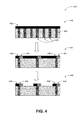
- FIG. 4 illustrates three different phases in manufacturing a multilayer circuit board with optical vias, arranged in accordance with at least some embodiments described herein.
- a circuit board according to embodiments may be manufactured in a variety of ways through sequential or parallel production steps.
- Diagram 400 of FIG. 4 and diagram 500 of FIG. 5 illustrate one example sequence of production steps. Of course, embodiments may be implemented employing other sequences, additional or fewer steps, and/or additional or fewer materials.
- Multilayer circuit board 442 may be at a stage of PCB manufacturing, where optical vias 406 can be formed in the circuit board through chemical, mechanical, or thermal methods.
- a conformal layer of a transparent conducting oxide ( 452 ) may be deposited on the top layer using lithography or similar techniques.
- the TCO layer may be formed using SnO 2 , ZnO, ITO, or similar materials.
- Multilayer circuit board 444 represents a subsequent phase of manufacturing, where the TCO layer 452 can be implanted with impurities creating p-n junctions 454 over the optical vias. Alternatively, the p-n junctions may be created inside the vias (at each end).
- the p-n junctions may be isolated to form diodes (photo emitting or detecting). While one side of the multilayer circuit board is shown in the diagrams, the process may be performed for both sides (top and bottom) simultaneously or sequentially such that corresponding photo-emitter/detector diode pairs are formed on both ends of each optical via.
- FIG. 5 illustrates two more phases in manufacturing of a multilayer circuit board with optical vias, in accordance with at least some embodiments of the present disclosure.
- Multilayer circuit board 562 of diagram 500 illustrates a subsequent phase of manufacturing, where planar dielectric layer is deposited over the top layer and the p-n junctions. The planarization may be accomplished by chemical or mechanical methods.
- electrical vias 574 may be drilled or etched in the dielectric layer 572 such that a connection is provided to each side ( 440 , 442 ) of the p-n junctions.
- the vias may be subsequently filled with a conductive material (e.g. a metal such as tungsten) for the electrical connection.
- FIG. 6 illustrates a general purpose computing device, which may be used to control manufacturing of a multilayer circuit board with optical vias for data transmission arranged in accordance with at least some embodiments of the present disclosure.
- Computer 600 includes a processor 610 , memory 620 , and one or more drives 630 .
- the drives 630 and their associated computer storage media such as removable storage media 634 (e.g., CD-ROM, DVD-ROM) and non-removable storage media 632 (e.g. a hard drive disk), may provide storage of computer readable instructions, data structures, program modules and other data for the computer 600 .
- Drives 630 may include an operating system 640 , application programs 650 , program modules 660 , and database 680 .
- Computer 600 further may include user input devices 690 through which a user may enter commands and data.
- Input devices 690 may include an electronic digitizer, a microphone 696 , a keyboard 694 , and a pointing device such as a mouse device 692 , trackball device or touch pad device.
- Other input devices may include a joystick device, game pad device, satellite dish, scanner device, or the like.
- Application programs 650 may include an optical via circuit board manufacturing application 652 , which may control automated circuit board production systems.
- Optical via circuit board manufacturing application 652 may provide instructions to different circuit board production modules for various phases of production such as etching, drilling, lamination, metallization, and comparable steps.
- User feedback through one of the input devices or in form of computer-readable instructions may be used to determine layout, materials, and other parameters of the circuit board design.
- Computers such as computer 600 may also include other peripheral output devices such as speakers 676 , printer 674 , and display 672 , which may be coupled through an output peripheral interface 670 or the like.
- Computer storage media includes, but is not limited to, RAM, ROM, EEPROM, flash memory or other memory technology, CD-ROM, digital versatile disks (DVD) or other optical storage, magnetic cassettes, magnetic tape, magnetic disk storage or other magnetic storage devices, or any other medium which may be used to store the desired information and which may be accessed by computer 600 . Any such computer storage media may be part of computer 600 .
- Computer 600 may operate in a networked environment using logical connections to one or more computers, such as a remote computer connected to network interface 606 .
- the remote computer may be a personal computer, a server, a router, a network PC, a peer device or other common network node, and can include many or all of the elements described above relative to computer 600 .
- Networking environments are commonplace in offices, enterprise-wide area networks (WAN), local area networks (LAN), intranets and world-wide networks such as the Internet.
- computer 600 may comprise the controller machine from which data is being migrated to multilayer circuit board manufacturing systems such as automatic drill systems, etching systems, etc., and the remote computer may comprise controllers of the systems.
- source and destination machines need not be coupled together by a network(s) 608 or any other means, but instead, data may be migrated via any media capable of being written by the source platform and read by the destination platform or platforms.
- computer 600 may be coupled to the LAN through network interface 606 or an adapter.
- the network(s) may comprise any topology employing servers, clients, switches, routers, modems, Internet service providers (ISPs), and any appropriate communication media (e.g., wired or wireless communications).
- a system may have a static or dynamic network topology.
- the network(s) may include a secure network such as an enterprise network (e.g., a LAN, WAN, or WLAN), an unsecure network such as a wireless open network (e.g., IEEE 802.11 wireless networks), or a world-wide network such (e.g., the Internet).
- the network(s) may also comprise a plurality of distinct networks that are adapted to operate together.
- the network(s) are adapted to provide communication between the nodes described herein.
- the network(s) may include wireless media such as acoustic, RF, infrared and other wireless media.
- the network communication link may be one example of a communication media.
- Communication media may typically be embodied by computer readable instructions, data structures, program modules, or other data in a modulated data signal, such as a carrier wave or other transport mechanism, and may include any information delivery media.
- a “modulated data signal” may be a signal that has one or more of its characteristics set or changed in such a manner as to encode information in the signal.
- communication media may include wired media such as a wired network or direct-wired connection, and wireless media such as acoustic, radio frequency (RF), microwave, infrared (IR) and other wireless media.
- RF radio frequency
- IR infrared
- the term computer readable media as used herein may include both storage media and communication media.
- Computer 600 may be implemented as a portion of a small-form factor portable (or mobile) electronic device such as a portable computing device, a mobile computing device, an application specific device, or a hybrid device that include any of the above functions.
- Computer 600 may also be implemented as a personal computer including both laptop computer and non-laptop computer configurations.
- computer 600 may be implemented as a networked system or as part of a general purpose or specialized server.
- FIG. 7 illustrates a special purpose processor, which may be used to control manufacturing of a multilayer circuit board with optical vias for data transmission, arranged in accordance with at least some embodiments of the present disclosure.
- Processor 710 of diagram 700 may be part of an automated circuit board manufacturing system communicatively coupled to one or more modules responsible for different phases of multilayer circuit board manufacturing process.
- Processor 710 may include a number of control modules configured to control different aspects of manufacturing a multilayer circuit board with optical vias according to some embodiments.
- deposition control module 730 may be configured to manage deposition of a transparent conducting oxide (TCO) layer on the top and bottom layers of the multilayer circuit board, in which p-n junctions may be formed as photo-emitter or photo-detector components over the vias for optical communication.
- Deposition control module 730 may be further configured to manage deposition of a dielectric layer over the patterned TCO layer such that electrical connections to the p-n junctions may be created through vias in the dielectric layer for connecting the p-n junctions to the electronic components on the circuit board.
- Implantation control module 740 may be configured to control implantation of the TCO layer with n-type or p-type impurities to create the p-n junctions.
- Etching control module 750 may be configured to manage chemical removal of optical via regions and/or conductive material on top and/or bottom conductive layers for forming the traces.
- Mechanical planarization control module 760 may be configured to control planarization of the TCO layer and/or the dielectric layer prior to filling of the optical vias with optically conducting material (e.g. glass) and the electrical vias with conductive material (e.g. metal).
- Metallization control module 770 may be configured to manage filling of the electrical vias with metallic material (pure metal or alloy).
- Memory 720 may be configured to store instructions for the control modules of processor 710 , which may be implemented as hardware, software, or combination of hardware and software.
- Processor 710 may be configured to communicate through electrical couplings or through networked communications (e.g., network(s) 790 ) with other computing devices and/or data stores such as storage facility 780 .
- networked communications e.g., network(s) 790
- Example embodiments may also include methods. These methods can be implemented in any number of ways, including the structures described herein. One such way is by machine operations, of devices of the type described in the present disclosure. Another optional way is for one or more of the individual operations of the methods to be performed in conjunction with one or more human operators performing some of the operations while other operations are performed by machines. These human operators need not be collocated with each other, but each can be only with a machine that performs a portion of the program. In other examples, the human interaction can be automated such as by pre-selected criteria that are machine automated.
- FIG. 8 is a flow diagram illustrating an example method that may be performed by a computing device, such as computer 600 in FIG. 6 or special purpose processor 710 in FIG. 7 .
- the operations described in blocks 822 through 836 may be stored as computer-executable instructions in a computer-readable medium such as drives 640 of computer 600 or memory 720 of processor 710 .
- a process of manufacturing a multilayer circuit board with optical vias for data transmission may begin with operation 822 , “CREATE REGIONS FOR OPTICAL VIA(S) IN MULTILAYER CIRCUIT BOARD.”
- holes may be drilled through mechanical, chemical, or other methods (e.g. laser drilling) on a multilayer circuit board for optical vias such as vias 206 in FIG. 2 .
- Operation 822 may be followed by operation 824 .
- TCO DEPOSIT TRANSPARENT CONDUCTING OXIDE (TCO) ON TOP LAYER” following operation 822 , a layer of TCO (layer 452 of FIG. 4 ) may be deposited on the top layer of the circuit board. According to other embodiments, the same operation may be repeated for the bottom layer of the multilayer circuit board. Operation 824 may be followed by operation 826 .
- n- or p-type impurities are impregnated into the TCO layer.
- p-n junctions are formed on the top (or bottom) layer of the multilayer circuit board about the optical vias 206 .
- the p-n junctions may be formed over the vias 206 or within the vias by injecting the material into the vias. Operation 826 may be followed by operation 828 .
- the p-n junctions are isolated into photo emitting or photo detecting diodes (or diode pairs) such as diodes 214 , 216 , 222 , 224 of FIG. 2 .
- photo emitting/detecting diode pairs may be used to transfer data between the electronic components with high bandwidth. Operation 828 may be followed by operation 830 .
- a layer of dielectric (layer 572 of FIG. 5 ) may be deposited on the top layer of the circuit board and the p-n junctions. Operation 830 may be followed by operation 832 .
- the dielectric layer may be planarized. Operation 832 may be followed by operation 834 .
- electrical connections can be created for the p-n junctions (or photo emitting/detecting diodes).
- the electrical connections may be created by drilling (or etching) vias 574 in the dielectric layer and metallizing those vias. Operation 834 may be followed by operation 836 .
- the multilayer circuit board may be populated with electronic components and connections established (e.g. soldering stage).
- data communication between the components may be at least partially accomplished through optical communication increasing bandwidth capacity while reducing supply current and noise compared to conventional components.
- Manufacturing a multilayer circuit board with optical vias may be implemented by similar processes with fewer or additional operations. In some examples, the operations may be performed in a different order. In some other examples, various operations may be eliminated. In still other examples, various operations may be divided into additional operations, or combined together into fewer operations.
- FIG. 9 illustrates a block diagram of an example computer program product, all arranged in accordance with at least some embodiments described herein.
- computer program product 900 may include a signal bearing medium 902 that may also include machine readable instructions 904 that, when executed by, for example, a processor, may provide the functionality described above with respect to FIG. 6 and FIG. 7 .
- the control modules 730 through 770 may undertake one or more of the tasks shown in FIG. 9 in response to instructions 904 conveyed to processor 710 by medium 702 to perform actions associated with manufacturing a multilayer circuit board with optical vias as described herein.
- Some of those instructions may include creating optical via regions, creating p-n junctions over the optical vias, and/or creating electrical connections to the p-n junctions (e.g. diodes).
- signal bearing medium 902 depicted in FIG. 9 may encompass a computer-readable medium 906 , such as, but not limited to, a hard disk drive, a Compact Disc (CD), a Digital Video Disk (DVD), a digital tape, memory, etc.
- signal bearing medium 902 may encompass a recordable medium 908 , such as, but not limited to, memory, read/write (R/W) CDs, R/W DVDs, etc.
- signal bearing medium 902 may encompass a communications medium 910 , such as, but not limited to, a digital and/or an analog communication medium (e.g., a fiber optic cable, a waveguide, a wired communications link, a wireless communication link, etc.).
- program product 900 may be conveyed to one or more modules of the processor 710 by an RF signal bearing medium 902 , where the signal bearing medium 902 is conveyed by a wireless communications medium 910 (e.g., a wireless communications medium conforming with the IEEE 802.11 standard).
- a wireless communications medium 910 e.g., a wireless communications medium conforming with the IEEE 802.11 standard.
- the present disclosure presents a multilayer circuit board with optical vias for data transmission between two or more layers according to some embodiments.
- the circuit board may include a circuit board 300 with two or more conductive layers 202 separated by a dielectric layer 204 , an optical via 214 for providing an optical transmission path between the two or more layers of the circuit board 300 , a photo-emitter component 216 coupled to one end of the optical via 214 and converting incident electrical signals to optical signals, and a photo-detector component 224 coupled to another end of the optical via 214 and converting the optical signals to received electrical signals.
- the photo-emitter component 216 may be either a light emitting diode (LED) or a laser diode.
- the photo-emitter component 216 may include a p-n junction formed in a transparent conducting oxide layer 452 deposited on a top layer of the circuit board 300 .
- the transparent conducting oxide layer 452 may include SnO 2 , ZnO, or ITO.
- the photo-detector component 224 may include one or more of a p-n junction photodiode, a p-i-n photodiode, an avalanche photodiode, and/or a metal-semiconductor-metal (MSM) photo-detector.
- MSM metal-semiconductor-metal
- the multilayer circuit board may further include an electrical component 220 electrically coupled to the photo-emitter component 216 and another electrical component 226 electrically coupled to the photo-detector component 224 .
- the optical via 214 may correspond to one member of an array of optical vias associated with the multilayer circuit board.
- the circuit board may include a number of conductive layers, where at least one of the optical vias may provide data transmission between a top conductive layer and an inner conductive layer.
- the present disclosure also describes a method for manufacturing a multilayer circuit board with optical vias for data transmission between two or more layers of the multilayer circuit board.
- the method may include creating one or more regions of the multilayer circuit board ( 822 ) for optical vias, depositing a transparent conducting oxide (TCO) layer on a top layer of the multilayer circuit board ( 824 ), creating p-n junctions about the regions for the optical vias ( 828 ), and creating electrical connections to the p-n junctions acting as light emitting diodes (LEDs) ( 834 ).
- TCO transparent conducting oxide
- the method may include depositing a transparent conducting oxide (TCO) layer 452 on a bottom layer of the multilayer circuit board, creating p-n junctions about the one or more regions for the optical vias ( 828 ), and creating electrical couplings to the p-n junctions acting as photodiodes ( 834 ).
- Creating the p-n junctions may include implanting the TCO layer with n-type impurities ( 826 ) and patterning the TCO layer to form the LEDs about the regions for the optical vias ( 828 ).
- creating the electrical connections to the p-n junctions may include depositing a dielectric layer over the patterned TCO layer ( 830 ) while leaving one or more regions for vias over the p-n junctions, planarizing the dielectric layer ( 832 ), and filling the vias with a metallic material to provide electrical connections to the LEDs ( 834 ).
- Electrical components may be placed on one or more of the top and/or bottom layers of the multilayer circuit board ( 836 ), and a p-n junction 336 may be formed in an inner layer of the multilayer circuit board, where an optical via 340 is used to couple a top layer of the multilayer circuit board 300 and the inner layer of the multilayer circuit board 300 .
- the present disclosure further describes an apparatus for controlling manufacturing of a multilayer circuit board 300 with optical vias 214 for data transmission between two or more layers of the multilayer circuit board 300 .
- the apparatus may include a memory with instructions stored thereon and a processor coupled to the memory and for executing the instructions.
- the instructions may cause the apparatus to create one or more regions for optical vias in the multilayer circuit board for data transmission between electrical components located on top and bottom layers of the multilayer circuit board ( 822 ), deposit a transparent conducting oxide (TCO) layer on the top and bottom layers of the multilayer circuit board ( 824 ), create p-n junctions about the regions for the optical via locations at the top and bottom layers ( 828 ) by implanting the TCO layer with n-type impurities ( 826 ), and create electrical couplings to the p-n junctions, where the p-n junctions are effective to act as either light emitting diodes (LEDs) or photodiodes ( 834 ).
- TCO transparent conducting oxide
- the apparatus may deposit a dielectric layer over the patterned TCO layer ( 830 ), planarize the dielectric layer ( 832 ), create one or more regions for vias over the p-n junctions, and fill the vias with a metallic material 574 to provide electrical connections to the LEDs ( 834 ).
- the apparatus may also place electrical components on the top and bottom layers of the multilayer circuit board ( 836 ) and couple at least some of the electrical components to the p-n junctions acting as LEDs and photodiodes.
- the dielectric layer 572 may be from tetraethyl orthosilicate (TEOS), and the metallic material 574 from tungsten.
- TEOS tetraethyl orthosilicate
- the vias and the optical vias may be formed in the respective regions for the vias and optical vias by one or more of etching and/or drilling.
- the implementer may opt for a mainly hardware and/or firmware vehicle; if flexibility is paramount, the implementer may opt for a mainly software implementation; or, yet again alternatively, the implementer may opt for some combination of hardware, software, and/or firmware.
- a signal bearing medium examples include, but are not limited to, the following: a recordable type medium such as a floppy disk, a hard disk drive, a Compact Disc (CD), a Digital Video Disk (DVD), a digital tape, a computer memory, etc.; and a transmission type medium such as a digital and/or an analog communication medium (e.g., a fiber optic cable, a waveguide, a wired communications link, a wireless communication link, etc.).
- a typical data processing system generally includes one or more of a system unit housing, a video display device, a memory such as volatile and non-volatile memory, processors such as microprocessors and digital signal processors, computational entities such as operating systems, drivers, graphical user interfaces, and applications programs, one or more interaction devices, such as a touch pad or screen, and/or control systems including feedback loops and control modules (e.g., adjusting manufacturing parameters of various phases of multilayer circuit board production).
- processors such as microprocessors and digital signal processors
- computational entities such as operating systems, drivers, graphical user interfaces, and applications programs
- interaction devices such as a touch pad or screen
- control systems including feedback loops and control modules (e.g., adjusting manufacturing parameters of various phases of multilayer circuit board production).
- a typical data processing system may be implemented utilizing any suitable commercially available components, such as those typically found in data computing/communication and/or network computing/communication systems.
- the herein described subject matter sometimes illustrates different components contained within, or connected with, different other components. It is to be understood that such depicted architectures are merely exemplary, and that in fact many other architectures may be implemented which achieve the same functionality. In a conceptual sense, any arrangement of components to achieve the same functionality is effectively “associated” such that the desired functionality is achieved. Hence, any two components herein combined to achieve a particular functionality may be seen as “associated with” each other such that the desired functionality is achieved, irrespective of architectures or intermediate components.
- any two components so associated may also be viewed as being “operably connected”, or “operably coupled”, to each other to achieve the desired functionality, and any two components capable of being so associated may also be viewed as being “operably couplable”, to each other to achieve the desired functionality.
- operably couplable include but are not limited to physically connectable and/or physically interacting components and/or wirelessly interactable and/or wirelessly interacting components and/or logically interacting and/or logically interactable components.
- a range includes each individual member.
- a group having 1-3 cells refers to groups having 1, 2, or 3 cells.
- a group having 1-5 cells refers to groups having 1, 2, 3, 4, or 5 cells, and so forth.
Abstract
Description
Claims (18)
Priority Applications (1)
| Application Number | Priority Date | Filing Date | Title |
|---|---|---|---|
| US14/169,145 US8933390B2 (en) | 2010-10-07 | 2014-01-30 | Data transmission through optical vias |
Applications Claiming Priority (1)
| Application Number | Priority Date | Filing Date | Title |
|---|---|---|---|
| PCT/US2010/051778 WO2012047220A1 (en) | 2010-10-07 | 2010-10-07 | Data transmission through optical vias |
Related Child Applications (1)
| Application Number | Title | Priority Date | Filing Date |
|---|---|---|---|
| US14/169,145 Continuation US8933390B2 (en) | 2010-10-07 | 2014-01-30 | Data transmission through optical vias |
Publications (2)
| Publication Number | Publication Date |
|---|---|
| US20130181110A1 US20130181110A1 (en) | 2013-07-18 |
| US8680458B2 true US8680458B2 (en) | 2014-03-25 |
Family
ID=45928006
Family Applications (2)
| Application Number | Title | Priority Date | Filing Date |
|---|---|---|---|
| US13/002,043 Expired - Fee Related US8680458B2 (en) | 2010-10-07 | 2010-10-07 | Data transmission through optical vias |
| US14/169,145 Expired - Fee Related US8933390B2 (en) | 2010-10-07 | 2014-01-30 | Data transmission through optical vias |
Family Applications After (1)
| Application Number | Title | Priority Date | Filing Date |
|---|---|---|---|
| US14/169,145 Expired - Fee Related US8933390B2 (en) | 2010-10-07 | 2014-01-30 | Data transmission through optical vias |
Country Status (2)
| Country | Link |
|---|---|
| US (2) | US8680458B2 (en) |
| WO (1) | WO2012047220A1 (en) |
Cited By (1)
| Publication number | Priority date | Publication date | Assignee | Title |
|---|---|---|---|---|
| US20140270627A1 (en) * | 2013-03-15 | 2014-09-18 | Compass Electro-Optical Systems Ltd. | Eo device for processing data signals |
Families Citing this family (6)
| Publication number | Priority date | Publication date | Assignee | Title |
|---|---|---|---|---|
| CN106132118B (en) * | 2016-07-13 | 2019-01-15 | 南京宏睿普林微波技术股份有限公司 | A kind of complex media method of manufacturing circuit board of multilayer dielectricity circuit |
| WO2018044257A1 (en) * | 2016-08-29 | 2018-03-08 | Intel Corporation | Resistive random access memory devices |
| WO2018044255A1 (en) * | 2016-08-29 | 2018-03-08 | Intel Corporation | Resistive random access memory devices |
| US11079408B2 (en) * | 2018-05-18 | 2021-08-03 | Tektronix, Inc. | Resistive test-probe tips |
| US10803396B2 (en) | 2018-06-19 | 2020-10-13 | Intel Corporation | Quantum circuit assemblies with Josephson junctions utilizing resistive switching materials |
| JP2023022422A (en) * | 2021-08-03 | 2023-02-15 | 日本メクトロン株式会社 | Method for manufacturing printed circuit board with electronic component, and printed circuit board with electronic component |
Citations (21)
| Publication number | Priority date | Publication date | Assignee | Title |
|---|---|---|---|---|
| GB2275576A (en) | 1993-02-26 | 1994-08-31 | Int Computers Ltd | Electronic circuit assembly with optically transmissive vias |
| US5564642A (en) | 1994-06-14 | 1996-10-15 | Agfa Geavert | Device for winding strips of photographic film |
| US5652811A (en) * | 1996-03-06 | 1997-07-29 | The United States Of America As Represented By The Secretary Of The Air Force | Semiconductor on fiber optic substrate (SOFOS) |
| US20040156576A1 (en) | 2003-02-11 | 2004-08-12 | Windover Lisa A. | Optical via to pass signals through a printed circuit board |
| US7095920B1 (en) | 2003-02-11 | 2006-08-22 | Little Optics Inc | Broadband optical via |
| US20070007584A1 (en) * | 2005-07-06 | 2007-01-11 | Samsung Electro-Mechanics Co., Ltd. | Nitride semiconductor light emitting diode and method of manufacturing the same |
| US7416979B2 (en) | 2001-07-25 | 2008-08-26 | Applied Materials, Inc. | Deposition methods for barrier and tungsten materials |
| US7471856B2 (en) | 2004-07-08 | 2008-12-30 | Dow Corning Corporation | Short reach optical interconnect |
| US7474825B1 (en) | 2008-03-03 | 2009-01-06 | International Business Machines Corporation | Circular grating resonator with integrated electro-optical modulation |
| US7486847B1 (en) | 2008-03-31 | 2009-02-03 | International Business Machines Corporation | Chip carrier package with optical vias |
| US7539376B2 (en) | 2002-11-27 | 2009-05-26 | International Business Machines Corporation | Optically connectable circuit board with optical component(s) mounted thereon |
| US7538358B2 (en) | 2003-10-15 | 2009-05-26 | Xloom Communications, Ltd. | Electro-optical circuitry having integrated connector and methods for the production thereof |
| US7583879B2 (en) | 2005-08-19 | 2009-09-01 | Infinera Corporation | Coupled optical waveguide resonators with heaters for thermo-optic control of wavelength and compound filter shape |
| US7616889B2 (en) | 2003-10-30 | 2009-11-10 | International Business Machines Corporation | Byte-wide optical backplane switching method |
| US7639912B2 (en) | 2007-01-31 | 2009-12-29 | Hewlett-Packard Development Company, L.P. | Apparatus and method for subterranean distribution of optical signals |
| US7639903B2 (en) | 2007-10-15 | 2009-12-29 | Hewlett-Packard Development Company, L.P. | Daisy chain optical interconnect |
| US20100024871A1 (en) | 2008-07-31 | 2010-02-04 | Min-Seok Oh | Photovoltaic device and method of manufacturing the same |
| US20100025362A1 (en) | 2008-05-02 | 2010-02-04 | Micron Technology, Inc. | Method of Forming Capacitors |
| US7658552B2 (en) | 2008-06-28 | 2010-02-09 | Kotura, Inc. | Interface between light source and optical component |
| US7704897B2 (en) | 2008-02-22 | 2010-04-27 | Applied Materials, Inc. | HDP-CVD SiON films for gap-fill |
| US7724759B2 (en) | 2002-11-27 | 2010-05-25 | International Business Machines Corporation | Method for the asynchronous arbitration of a high frequency bus in a long latency environment |
Family Cites Families (2)
| Publication number | Priority date | Publication date | Assignee | Title |
|---|---|---|---|---|
| WO1994006052A1 (en) * | 1992-09-10 | 1994-03-17 | Fujitsu Limited | Optical circuit system and its constituents |
| US5864642A (en) * | 1997-02-10 | 1999-01-26 | Motorola, Inc. | Electro-optic device board |
-
2010
- 2010-10-07 WO PCT/US2010/051778 patent/WO2012047220A1/en active Application Filing
- 2010-10-07 US US13/002,043 patent/US8680458B2/en not_active Expired - Fee Related
-
2014
- 2014-01-30 US US14/169,145 patent/US8933390B2/en not_active Expired - Fee Related
Patent Citations (25)
| Publication number | Priority date | Publication date | Assignee | Title |
|---|---|---|---|---|
| GB2275576A (en) | 1993-02-26 | 1994-08-31 | Int Computers Ltd | Electronic circuit assembly with optically transmissive vias |
| US5564642A (en) | 1994-06-14 | 1996-10-15 | Agfa Geavert | Device for winding strips of photographic film |
| US5652811A (en) * | 1996-03-06 | 1997-07-29 | The United States Of America As Represented By The Secretary Of The Air Force | Semiconductor on fiber optic substrate (SOFOS) |
| US7416979B2 (en) | 2001-07-25 | 2008-08-26 | Applied Materials, Inc. | Deposition methods for barrier and tungsten materials |
| US7724759B2 (en) | 2002-11-27 | 2010-05-25 | International Business Machines Corporation | Method for the asynchronous arbitration of a high frequency bus in a long latency environment |
| US7551453B2 (en) | 2002-11-27 | 2009-06-23 | International Business Machines Corporation | Optically connectable circuit board with optical component(s) mounted thereon |
| US7539376B2 (en) | 2002-11-27 | 2009-05-26 | International Business Machines Corporation | Optically connectable circuit board with optical component(s) mounted thereon |
| US7263248B2 (en) | 2003-02-11 | 2007-08-28 | Avago Technologies Fiber Ip (Singapore) Pte. Ltd. | Optical via to pass signals through a printed circuit board |
| US20070258676A1 (en) | 2003-02-11 | 2007-11-08 | Windover Lisa A | Optical via to pass signals through a printed circuit board |
| US20040156576A1 (en) | 2003-02-11 | 2004-08-12 | Windover Lisa A. | Optical via to pass signals through a printed circuit board |
| US7546007B2 (en) | 2003-02-11 | 2009-06-09 | Infinera Corporation | Broadband optical via |
| US7095920B1 (en) | 2003-02-11 | 2006-08-22 | Little Optics Inc | Broadband optical via |
| US7538358B2 (en) | 2003-10-15 | 2009-05-26 | Xloom Communications, Ltd. | Electro-optical circuitry having integrated connector and methods for the production thereof |
| US7616889B2 (en) | 2003-10-30 | 2009-11-10 | International Business Machines Corporation | Byte-wide optical backplane switching method |
| US7471856B2 (en) | 2004-07-08 | 2008-12-30 | Dow Corning Corporation | Short reach optical interconnect |
| US20070007584A1 (en) * | 2005-07-06 | 2007-01-11 | Samsung Electro-Mechanics Co., Ltd. | Nitride semiconductor light emitting diode and method of manufacturing the same |
| US7583879B2 (en) | 2005-08-19 | 2009-09-01 | Infinera Corporation | Coupled optical waveguide resonators with heaters for thermo-optic control of wavelength and compound filter shape |
| US7639912B2 (en) | 2007-01-31 | 2009-12-29 | Hewlett-Packard Development Company, L.P. | Apparatus and method for subterranean distribution of optical signals |
| US7639903B2 (en) | 2007-10-15 | 2009-12-29 | Hewlett-Packard Development Company, L.P. | Daisy chain optical interconnect |
| US7704897B2 (en) | 2008-02-22 | 2010-04-27 | Applied Materials, Inc. | HDP-CVD SiON films for gap-fill |
| US7474825B1 (en) | 2008-03-03 | 2009-01-06 | International Business Machines Corporation | Circular grating resonator with integrated electro-optical modulation |
| US7486847B1 (en) | 2008-03-31 | 2009-02-03 | International Business Machines Corporation | Chip carrier package with optical vias |
| US20100025362A1 (en) | 2008-05-02 | 2010-02-04 | Micron Technology, Inc. | Method of Forming Capacitors |
| US7658552B2 (en) | 2008-06-28 | 2010-02-09 | Kotura, Inc. | Interface between light source and optical component |
| US20100024871A1 (en) | 2008-07-31 | 2010-02-04 | Min-Seok Oh | Photovoltaic device and method of manufacturing the same |
Non-Patent Citations (8)
| Title |
|---|
| Claudio Favi and Edoardo Charbon, Techniques for Fully Integrated Intra-/Inter-Chip Optical Communication, Proceedings of the 45th annual Design Automation Conference, Anaheim, California, 2008, pp: 343-344. |
| International Preliminary Report on Patentability issued on Apr. 9, 2013. |
| International Search Report and Written Opinion dated Dec. 16, 2010 in PCT/US2010/051778. |
| Morioka, Y. et al., "An Approach to Slurry Characterization for CMP," vol. 11, pp. 153-155, 2004 http://www.nittahaas.com/technology/pdf/200421.pdf. |
| TimeDomain CDV, Inc. "Plasma-Enhanced Deposition from TEOS and Oxygen" accessed from http://www.timedomaincvd.com/CVD-Fundamentals/films/PECVD-TEOS.html; Retrieved on Nov. 4, 2012. |
| TimeDomain CDV, Inc. "Plasma-Enhanced Deposition from TEOS and Oxygen" accessed from http://www.timedomaincvd.com/CVD—Fundamentals/films/PECVD—TEOS.html; Retrieved on Nov. 4, 2012. |
| Wang et al., Session DD: P-Type Doping and Electroluminescence in ZnO Band Edge Electroluminescence from N+-Implanted Bulk ZnO, Department of Chemical Engineering, University of Florida, Gainesville, FL 3261, Pennsylvania State University, University Park, PA, Jun. 30, 2006. |
| Zhou et al., Indium Tin Oxide (ITO) Deposition, Patterning and Schottky Contact Fabrication, A thesis submitted in partial fulfillment of the requirements for the degree of Master of Science in Microelectric Engineering, Department of Microelectric Engineering, College of Engineering, Rochester, New York Dec. 2005, 89 pages. |
Cited By (2)
| Publication number | Priority date | Publication date | Assignee | Title |
|---|---|---|---|---|
| US20140270627A1 (en) * | 2013-03-15 | 2014-09-18 | Compass Electro-Optical Systems Ltd. | Eo device for processing data signals |
| US9304272B2 (en) * | 2013-03-15 | 2016-04-05 | Compass Electro Optical Systems Ltd. | EO device for processing data signals |
Also Published As
| Publication number | Publication date |
|---|---|
| US8933390B2 (en) | 2015-01-13 |
| US20130181110A1 (en) | 2013-07-18 |
| US20140145189A1 (en) | 2014-05-29 |
| WO2012047220A1 (en) | 2012-04-12 |
Similar Documents
| Publication | Publication Date | Title |
|---|---|---|
| US8933390B2 (en) | Data transmission through optical vias | |
| US9490240B2 (en) | Film interposer for integrated circuit devices | |
| US8324722B2 (en) | Packaging device for matrix-arrayed semiconductor light-emitting elements of high power and high directivity | |
| CN108364926B (en) | With hierarchical interconnections bridge interconnection of structures | |
| JP5224845B2 (en) | Semiconductor device manufacturing method and semiconductor device | |
| CN103915402A (en) | Photoelectric module structure | |
| CN101346039B (en) | Novel via structure for improving signal integrity | |
| US11107770B1 (en) | Integrated electrical/optical interface with two-tiered packaging | |
| CN104220910A (en) | Interchip communication using embedded dielectric and metal waveguides | |
| US8295058B2 (en) | Structure for enhancing reference return current conduction | |
| US20150282317A1 (en) | Edge contacts of circuit boards, and related apparatus and methods | |
| US20200350234A1 (en) | Functional stiffener that enables land grid array interconnections and power decoupling | |
| JP2013197479A (en) | Tosa module package | |
| CN102593313A (en) | Package carrier and method for manufacturing the same | |
| JP5277874B2 (en) | Opto-electric hybrid board and electronic equipment | |
| US7450793B2 (en) | Semiconductor device integrated with opto-electric component and method for fabricating the same | |
| CN104425286A (en) | IC carrier plate, semiconductor device having the same and manufacturing method of the IC carrier plate | |
| CN103762205B (en) | Multifunctional base plate based on PCB technology and manufacturing method thereof | |
| JP2020500430A (en) | Consistency drive device for multibeam optoelectronic arrays | |
| KR101259308B1 (en) | Heterostructure containing ic and led and method for fabricating the same | |
| CN105578711A (en) | Wiring board | |
| CN102436042A (en) | Flexible-coupling high-speed photoelectric device | |
| JP4496825B2 (en) | Semiconductor device and manufacturing method thereof | |
| CN212628597U (en) | PCB structure of via hole under optimization BGA | |
| WO2012040743A2 (en) | Electrolytic gold or gold palladium surface finish application in coreless substrate processing |
Legal Events
| Date | Code | Title | Description |
|---|---|---|---|
| AS | Assignment |
Owner name: H&C SCIENTIFIC RESOURCES INTERNATIONAL, COLORADO Free format text: ASSIGNMENT OF ASSIGNORS INTEREST;ASSIGNOR:SIEVERS, MICHAEL RAY;REEL/FRAME:025611/0432 Effective date: 20101006 |
|
| AS | Assignment |
Owner name: EMPIRE TECHNOLOGY DEVELOPMENT, LLC, DELAWARE Free format text: ASSIGNMENT OF ASSIGNORS INTEREST;ASSIGNOR:H&C SCIENTIFIC RESOURCES INTERNATIONAL, LLC;REEL/FRAME:025703/0803 Effective date: 20110119 Owner name: EMPIRE TECHNOLOGY DEVELOPMENT, LLC, DELAWARE Free format text: ASSIGNMENT OF ASSIGNORS INTEREST;ASSIGNOR:H&C SCIENTIFIC RESOURCES INTERNATIONAL, LLC;REEL/FRAME:025703/0722 Effective date: 20110119 Owner name: H&C SCIENTIFIC RESOURCES INTERNATIONAL, LLC, COLOR Free format text: ASSIGNMENT OF ASSIGNORS INTEREST;ASSIGNOR:SIEVERS, MICHAEL RAY;REEL/FRAME:025703/0754 Effective date: 20110119 Owner name: H&C SCIENTIFIC RESOURCES INTERNATIONAL, LLC, COLOR Free format text: ASSIGNMENT OF ASSIGNORS INTEREST;ASSIGNOR:SIEVERS, MICHAEL RAY;REEL/FRAME:025703/0711 Effective date: 20110119 |
|
| STCF | Information on status: patent grant |
Free format text: PATENTED CASE |
|
| CC | Certificate of correction | ||
| MAFP | Maintenance fee payment |
Free format text: PAYMENT OF MAINTENANCE FEE, 4TH YEAR, LARGE ENTITY (ORIGINAL EVENT CODE: M1551) Year of fee payment: 4 |
|
| AS | Assignment |
Owner name: CRESTLINE DIRECT FINANCE, L.P., TEXAS Free format text: SECURITY INTEREST;ASSIGNOR:EMPIRE TECHNOLOGY DEVELOPMENT LLC;REEL/FRAME:048373/0217 Effective date: 20181228 |
|
| FEPP | Fee payment procedure |
Free format text: MAINTENANCE FEE REMINDER MAILED (ORIGINAL EVENT CODE: REM.); ENTITY STATUS OF PATENT OWNER: LARGE ENTITY |
|
| LAPS | Lapse for failure to pay maintenance fees |
Free format text: PATENT EXPIRED FOR FAILURE TO PAY MAINTENANCE FEES (ORIGINAL EVENT CODE: EXP.); ENTITY STATUS OF PATENT OWNER: LARGE ENTITY |
|
| STCH | Information on status: patent discontinuation |
Free format text: PATENT EXPIRED DUE TO NONPAYMENT OF MAINTENANCE FEES UNDER 37 CFR 1.362 |
|
| FP | Lapsed due to failure to pay maintenance fee |
Effective date: 20220325 |