US8665629B2 - Condensed memory cell structure using a FinFET - Google Patents
Condensed memory cell structure using a FinFET Download PDFInfo
- Publication number
- US8665629B2 US8665629B2 US11/864,575 US86457507A US8665629B2 US 8665629 B2 US8665629 B2 US 8665629B2 US 86457507 A US86457507 A US 86457507A US 8665629 B2 US8665629 B2 US 8665629B2
- Authority
- US
- United States
- Prior art keywords
- memory element
- source
- select transistor
- drain
- resistivity changing
- Prior art date
- Legal status (The legal status is an assumption and is not a legal conclusion. Google has not performed a legal analysis and makes no representation as to the accuracy of the status listed.)
- Active, expires
Links
- 230000015654 memory Effects 0.000 title claims abstract description 296
- 239000000758 substrate Substances 0.000 claims abstract description 52
- 229910052799 carbon Inorganic materials 0.000 claims description 33
- OKTJSMMVPCPJKN-UHFFFAOYSA-N Carbon Chemical compound [C] OKTJSMMVPCPJKN-UHFFFAOYSA-N 0.000 claims description 32
- 125000006850 spacer group Chemical group 0.000 claims description 29
- 229910000314 transition metal oxide Inorganic materials 0.000 claims description 7
- 230000008878 coupling Effects 0.000 claims description 3
- 238000010168 coupling process Methods 0.000 claims description 3
- 238000005859 coupling reaction Methods 0.000 claims description 3
- 230000003993 interaction Effects 0.000 claims description 3
- 238000000034 method Methods 0.000 abstract description 80
- 238000004519 manufacturing process Methods 0.000 abstract description 11
- 239000010410 layer Substances 0.000 description 77
- 239000000463 material Substances 0.000 description 65
- 108091006146 Channels Proteins 0.000 description 41
- 230000008569 process Effects 0.000 description 34
- 238000000151 deposition Methods 0.000 description 24
- 229910052710 silicon Inorganic materials 0.000 description 23
- XUIMIQQOPSSXEZ-UHFFFAOYSA-N Silicon Chemical compound [Si] XUIMIQQOPSSXEZ-UHFFFAOYSA-N 0.000 description 21
- 239000010703 silicon Substances 0.000 description 21
- 238000002425 crystallisation Methods 0.000 description 20
- 230000008025 crystallization Effects 0.000 description 20
- 238000005530 etching Methods 0.000 description 20
- 238000005516 engineering process Methods 0.000 description 18
- 230000015572 biosynthetic process Effects 0.000 description 12
- 239000003989 dielectric material Substances 0.000 description 11
- 150000004767 nitrides Chemical class 0.000 description 11
- 239000004020 conductor Substances 0.000 description 10
- 239000002019 doping agent Substances 0.000 description 10
- 229910052751 metal Inorganic materials 0.000 description 10
- 239000002184 metal Substances 0.000 description 10
- 238000003860 storage Methods 0.000 description 10
- 230000008859 change Effects 0.000 description 9
- 229910003481 amorphous carbon Inorganic materials 0.000 description 7
- 239000011810 insulating material Substances 0.000 description 7
- 238000002955 isolation Methods 0.000 description 7
- 230000005415 magnetization Effects 0.000 description 7
- 229910052698 phosphorus Inorganic materials 0.000 description 7
- 229910052787 antimony Inorganic materials 0.000 description 6
- 229910052785 arsenic Inorganic materials 0.000 description 6
- 229910052796 boron Inorganic materials 0.000 description 6
- 238000001465 metallisation Methods 0.000 description 6
- ZOXJGFHDIHLPTG-UHFFFAOYSA-N Boron Chemical compound [B] ZOXJGFHDIHLPTG-UHFFFAOYSA-N 0.000 description 5
- OAICVXFJPJFONN-UHFFFAOYSA-N Phosphorus Chemical compound [P] OAICVXFJPJFONN-UHFFFAOYSA-N 0.000 description 5
- WATWJIUSRGPENY-UHFFFAOYSA-N antimony atom Chemical compound [Sb] WATWJIUSRGPENY-UHFFFAOYSA-N 0.000 description 5
- RQNWIZPPADIBDY-UHFFFAOYSA-N arsenic atom Chemical compound [As] RQNWIZPPADIBDY-UHFFFAOYSA-N 0.000 description 5
- 230000000694 effects Effects 0.000 description 5
- 238000000059 patterning Methods 0.000 description 5
- 239000011574 phosphorus Substances 0.000 description 5
- 238000012545 processing Methods 0.000 description 5
- PNEYBMLMFCGWSK-UHFFFAOYSA-N aluminium oxide Inorganic materials [O-2].[O-2].[O-2].[Al+3].[Al+3] PNEYBMLMFCGWSK-UHFFFAOYSA-N 0.000 description 4
- 229910052593 corundum Inorganic materials 0.000 description 4
- 230000008021 deposition Effects 0.000 description 4
- 238000010438 heat treatment Methods 0.000 description 4
- 239000012212 insulator Substances 0.000 description 4
- 238000005468 ion implantation Methods 0.000 description 4
- 239000007769 metal material Substances 0.000 description 4
- 229910001845 yogo sapphire Inorganic materials 0.000 description 4
- 229910045601 alloy Inorganic materials 0.000 description 3
- 239000000956 alloy Substances 0.000 description 3
- 238000005229 chemical vapour deposition Methods 0.000 description 3
- 230000002860 competitive effect Effects 0.000 description 3
- 238000009826 distribution Methods 0.000 description 3
- 238000002513 implantation Methods 0.000 description 3
- 230000003647 oxidation Effects 0.000 description 3
- 238000007254 oxidation reaction Methods 0.000 description 3
- 229910003321 CoFe Inorganic materials 0.000 description 2
- 229910001030 Iron–nickel alloy Inorganic materials 0.000 description 2
- 229910019041 PtMn Inorganic materials 0.000 description 2
- 239000002194 amorphous carbon material Substances 0.000 description 2
- 230000002457 bidirectional effect Effects 0.000 description 2
- 239000003575 carbonaceous material Substances 0.000 description 2
- 229910052804 chromium Inorganic materials 0.000 description 2
- 238000004891 communication Methods 0.000 description 2
- 238000013461 design Methods 0.000 description 2
- 238000010586 diagram Methods 0.000 description 2
- 229910052735 hafnium Inorganic materials 0.000 description 2
- 238000002347 injection Methods 0.000 description 2
- 239000007924 injection Substances 0.000 description 2
- 239000011229 interlayer Substances 0.000 description 2
- 238000001459 lithography Methods 0.000 description 2
- 230000008018 melting Effects 0.000 description 2
- 238000002844 melting Methods 0.000 description 2
- 239000000203 mixture Substances 0.000 description 2
- 238000012986 modification Methods 0.000 description 2
- 230000004048 modification Effects 0.000 description 2
- 229910052750 molybdenum Inorganic materials 0.000 description 2
- 229910052758 niobium Inorganic materials 0.000 description 2
- 229910052760 oxygen Inorganic materials 0.000 description 2
- 229910021420 polycrystalline silicon Inorganic materials 0.000 description 2
- 229920005591 polysilicon Polymers 0.000 description 2
- 239000004065 semiconductor Substances 0.000 description 2
- 229910021332 silicide Inorganic materials 0.000 description 2
- FVBUAEGBCNSCDD-UHFFFAOYSA-N silicide(4-) Chemical compound [Si-4] FVBUAEGBCNSCDD-UHFFFAOYSA-N 0.000 description 2
- 229910052717 sulfur Inorganic materials 0.000 description 2
- 229910052715 tantalum Inorganic materials 0.000 description 2
- 229910052719 titanium Inorganic materials 0.000 description 2
- 229910052721 tungsten Inorganic materials 0.000 description 2
- 229910052720 vanadium Inorganic materials 0.000 description 2
- 229910052726 zirconium Inorganic materials 0.000 description 2
- 229910000763 AgInSbTe Inorganic materials 0.000 description 1
- 229910005542 GaSb Inorganic materials 0.000 description 1
- 229910005872 GeSb Inorganic materials 0.000 description 1
- 229910000618 GeSbTe Inorganic materials 0.000 description 1
- 229910005900 GeTe Inorganic materials 0.000 description 1
- 108090000699 N-Type Calcium Channels Proteins 0.000 description 1
- 102000004129 N-Type Calcium Channels Human genes 0.000 description 1
- 108010075750 P-Type Calcium Channels Proteins 0.000 description 1
- 229910018321 SbTe Inorganic materials 0.000 description 1
- 229910010037 TiAlN Inorganic materials 0.000 description 1
- 229910008482 TiSiN Inorganic materials 0.000 description 1
- 230000004913 activation Effects 0.000 description 1
- 229910052782 aluminium Inorganic materials 0.000 description 1
- 238000013459 approach Methods 0.000 description 1
- 238000003491 array Methods 0.000 description 1
- 229910052797 bismuth Inorganic materials 0.000 description 1
- 125000004432 carbon atom Chemical group C* 0.000 description 1
- 229910052798 chalcogen Inorganic materials 0.000 description 1
- -1 chalcogenide compound Chemical class 0.000 description 1
- 150000004770 chalcogenides Chemical class 0.000 description 1
- 150000001787 chalcogens Chemical class 0.000 description 1
- 238000006243 chemical reaction Methods 0.000 description 1
- 238000007796 conventional method Methods 0.000 description 1
- 239000012777 electrically insulating material Substances 0.000 description 1
- 238000007667 floating Methods 0.000 description 1
- 229910052732 germanium Inorganic materials 0.000 description 1
- 229910052738 indium Inorganic materials 0.000 description 1
- WPYVAWXEWQSOGY-UHFFFAOYSA-N indium antimonide Chemical compound [Sb]#[In] WPYVAWXEWQSOGY-UHFFFAOYSA-N 0.000 description 1
- QRXWMOHMRWLFEY-UHFFFAOYSA-N isoniazide Chemical compound NNC(=O)C1=CC=NC=C1 QRXWMOHMRWLFEY-UHFFFAOYSA-N 0.000 description 1
- 229910052745 lead Inorganic materials 0.000 description 1
- 238000005259 measurement Methods 0.000 description 1
- 229910052757 nitrogen Inorganic materials 0.000 description 1
- 230000008520 organization Effects 0.000 description 1
- 230000000737 periodic effect Effects 0.000 description 1
- 230000002093 peripheral effect Effects 0.000 description 1
- 239000012782 phase change material Substances 0.000 description 1
- 229910052711 selenium Inorganic materials 0.000 description 1
- 238000000926 separation method Methods 0.000 description 1
- 229910052718 tin Inorganic materials 0.000 description 1
Images


Classifications
-
- H—ELECTRICITY
- H01—ELECTRIC ELEMENTS
- H01L—SEMICONDUCTOR DEVICES NOT COVERED BY CLASS H10
- H01L29/00—Semiconductor devices adapted for rectifying, amplifying, oscillating or switching, or capacitors or resistors with at least one potential-jump barrier or surface barrier, e.g. PN junction depletion layer or carrier concentration layer; Details of semiconductor bodies or of electrodes thereof ; Multistep manufacturing processes therefor
- H01L29/66—Types of semiconductor device ; Multistep manufacturing processes therefor
- H01L29/66007—Multistep manufacturing processes
- H01L29/66075—Multistep manufacturing processes of devices having semiconductor bodies comprising group 14 or group 13/15 materials
- H01L29/66227—Multistep manufacturing processes of devices having semiconductor bodies comprising group 14 or group 13/15 materials the devices being controllable only by the electric current supplied or the electric potential applied, to an electrode which does not carry the current to be rectified, amplified or switched, e.g. three-terminal devices
- H01L29/66409—Unipolar field-effect transistors
- H01L29/66477—Unipolar field-effect transistors with an insulated gate, i.e. MISFET
- H01L29/66787—Unipolar field-effect transistors with an insulated gate, i.e. MISFET with a gate at the side of the channel
- H01L29/66795—Unipolar field-effect transistors with an insulated gate, i.e. MISFET with a gate at the side of the channel with a horizontal current flow in a vertical sidewall of a semiconductor body, e.g. FinFET, MuGFET
-
- H—ELECTRICITY
- H10—SEMICONDUCTOR DEVICES; ELECTRIC SOLID-STATE DEVICES NOT OTHERWISE PROVIDED FOR
- H10B—ELECTRONIC MEMORY DEVICES
- H10B61/00—Magnetic memory devices, e.g. magnetoresistive RAM [MRAM] devices
- H10B61/20—Magnetic memory devices, e.g. magnetoresistive RAM [MRAM] devices comprising components having three or more electrodes, e.g. transistors
- H10B61/22—Magnetic memory devices, e.g. magnetoresistive RAM [MRAM] devices comprising components having three or more electrodes, e.g. transistors of the field-effect transistor [FET] type
-
- H—ELECTRICITY
- H10—SEMICONDUCTOR DEVICES; ELECTRIC SOLID-STATE DEVICES NOT OTHERWISE PROVIDED FOR
- H10B—ELECTRONIC MEMORY DEVICES
- H10B63/00—Resistance change memory devices, e.g. resistive RAM [ReRAM] devices
- H10B63/30—Resistance change memory devices, e.g. resistive RAM [ReRAM] devices comprising selection components having three or more electrodes, e.g. transistors
-
- H—ELECTRICITY
- H01—ELECTRIC ELEMENTS
- H01L—SEMICONDUCTOR DEVICES NOT COVERED BY CLASS H10
- H01L29/00—Semiconductor devices adapted for rectifying, amplifying, oscillating or switching, or capacitors or resistors with at least one potential-jump barrier or surface barrier, e.g. PN junction depletion layer or carrier concentration layer; Details of semiconductor bodies or of electrodes thereof ; Multistep manufacturing processes therefor
- H01L29/66—Types of semiconductor device ; Multistep manufacturing processes therefor
- H01L29/68—Types of semiconductor device ; Multistep manufacturing processes therefor controllable by only the electric current supplied, or only the electric potential applied, to an electrode which does not carry the current to be rectified, amplified or switched
- H01L29/76—Unipolar devices, e.g. field effect transistors
- H01L29/772—Field effect transistors
- H01L29/78—Field effect transistors with field effect produced by an insulated gate
- H01L29/785—Field effect transistors with field effect produced by an insulated gate having a channel with a horizontal current flow in a vertical sidewall of a semiconductor body, e.g. FinFET, MuGFET
Definitions
- Non-volatile memory which retains its stored data even when power is not present, may be used.
- non-volatile memory is typically used in digital cameras, portable audio players, wireless communication devices, personal digital assistants, and peripheral devices, as well as for storing firmware in computers and other devices.
- Non-volatile memory technologies include flash memory, magnetoresistive random access memory (MRAM), phase change random access memory (PCRAM), and conductive bridging random access memory (CBRAM). Due to the great demand for memory devices, researchers are continually improving memory technology and developing new types of memory, including new types of non-volatile memory.
- MRAM magnetoresistive random access memory
- PCRAM phase change random access memory
- CBRAM conductive bridging random access memory
- FIG. 1 shows a portion of a conventional magnetoresistive memory (MRAM) device
- FIG. 2 show a conventional phase changing (PCRAM) memory element
- FIG. 3 shows a block diagram of a memory device using resistivity changing memory elements
- FIGS. 4A and 4B illustrate the operation of a carbon memory cell
- FIGS. 5A and 5B show schematic representations of a memory cell including a resistivity changing memory element and a select transistor
- FIG. 6 shows the layout of a conventional thermal select MRAM cell
- FIGS. 7A and 7B illustrate a FinFET of a type that may be suitable for use with some embodiments of the invention
- FIGS. 8A-8C show an example integrated circuit memory device according to an embodiment of the invention.
- FIGS. 9A and 9B are graphs of estimated FinFET height vs. write current, in accordance with an embodiment of the invention.
- FIGS. 10A-10L show various steps in a front-end-of-line (FEOL) process for manufacturing an integrated circuit memory device according to an embodiment of the invention
- FIGS. 11A-11M show steps in a FEOL process for manufacturing an integrated circuit memory device according to another embodiment of the invention.
- FIGS. 12A-12C show an integrated circuit memory device in which two FinFETs are used to drive the switching current of a resistivity changing memory element, in accordance with an embodiment of the invention
- FIGS. 13A-13I show steps in a back-end-of-line (BEOL) process for manufacturing an integrated circuit memory device in accordance with an embodiment of the invention.
- FIGS. 14A and 14B show a memory module that may include an integrated circuit memory device according to an embodiment of the invention.
- FIG. 1 shows a perspective view of an MRAM array 100 having bit lines 102 disposed in an orthogonal direction to word lines 104 in adjacent metallization layers.
- Magnetoresistive memory elements 106 are electrically coupled to the bit lines 102 and word lines 104 , and are positioned between the bit lines 102 and word lines 104 at locations where a bit line 102 crosses a word line 104 .
- the magnetoresistive memory elements 106 may include a free layer 108 , a tunnel layer 110 , and a fixed layer 112 .
- the free layer 108 and fixed layer 112 may each include a plurality of magnetic metal layers (not shown). These magnetic metal layers may, for example, include eight to twelve layers of materials such as PtMn, CoFe, Ru, and NiFe.
- the tunnel layer 110 may include a dielectric, such as Al 2 O 3 .
- the fixed layer 112 may be magnetized in a fixed direction, while the direction of magnetization of the free layer 108 may be switched, changing the resistance of the magnetoresistive memory element 106 .
- One bit of digital information may be stored in a magnetoresistive memory element 106 by running a current in the appropriate direction through the bit line 102 and the word line 104 that intersect at the selected magnetoresistive memory element 106 , creating a sufficient magnetic field to set the direction of magnetization of the free layer 108 .
- Information may be read from a magnetoresistive memory element 106 by applying a voltage across the memory element, and measuring the resistance.
- the measured resistance may be low, representing a value of “0” for the bit. If the direction of magnetization of the free layer 108 is anti-parallel to the direction of magnetization of the fixed layer 112 , then the resistance may be high, representing a value of “1”.
- thermal select MRAM devices switching of the free layer is facilitated by using a heating current to heat the free layer to a temperature that permits its direction of magnetization to be more easily switched. This can be used, for example, to prevent inadvertent switching of nearby cells in a densely-packed MRAM array.
- thermal select MRAM cells may include a transistor, as well as a magnetoresistive memory element. The transistor may be used to select the cell, and to drive the current that is used for heating the cell.
- a word line may be used to select a cell by being electrically connected to the gate of the transistor, so that a heating current flows through the cell from the bit line when the transistor is selected.
- the select transistor may also be used for selecting the read current path to read out the cell resistance.
- Such a select transistor may also be used in spin-injection MRAM memory cells, or other types of MRAM cells. Other variations that include a variety of components in the design of a memory cell also are possible.
- FIG. 1 represents only a small portion of an actual MRAM device.
- a 1 Mb MRAM device i.e., an MRAM device storing approximately one million bits of data
- phase change random access memory is known as phase change random access memory (PCRAM).
- the resistivity changing memory elements used in PCRAM are phase changing memory elements that include a phase changing material.
- the phase changing material can be switched between at least two different crystallization states (i.e., the phase changing material may adopt at least two different degrees of crystallization), wherein each crystallization state may be used to represent a memory state.
- the crystallization state having a high degree of crystallization is also referred to as a “crystalline state”
- crystallization state having a low degree of crystallization is also referred to as an “amorphous state”.
- Different crystallization states can be distinguished from each other by their differing electrical properties, and in particular by their different resistances.
- a crystallization state having a high degree of crystallization generally has a lower resistance than a crystallization state having a low degree of crystallization (disordered atomic structure).
- the phase changing material can adopt two crystallization states (an “amorphous state” and a “crystalline state”), however it will be understood that additional intermediate states also may be used.
- Phase changing memory elements may change from the amorphous state to the crystalline state (and vice versa) due to temperature changes of the phase changing material. These temperature changes may be caused using different approaches. For example, a current may be driven through the phase changing material (or a voltage may be applied across the phase changing material). Alternatively, a current or a voltage may be fed to a resistive heater which is disposed adjacent to the phase changing material. To determine the memory state of a resistivity changing memory element, a sensing current may routed through the phase changing material (or a sensing voltage may be applied across the phase changing material), thereby sensing the resistivity of the resistivity changing memory element, which represents the memory state of the memory element.
- FIG. 2 illustrates a cross-sectional view of an exemplary phase changing memory element 200 (active-in-via type).
- the phase changing memory element 200 includes a first electrode 202 , a phase changing material 204 , a second electrode 206 , and an insulating material 208 .
- the phase changing material 204 is laterally enclosed by the insulating material 208 .
- a selection device such as a transistor, a diode, or another active device, may be coupled to the first electrode 202 or to the second electrode 206 to control the application of a current or a voltage to the phase changing material 204 via the first electrode 202 and/or the second electrode 206 .
- a current pulse and/or voltage pulse may be applied to the phase changing material 204 , wherein the pulse parameters are chosen such that the phase changing material 204 is heated above its crystallization temperature, while keeping the temperature below the melting temperature of the phase changing material 204 .
- a current pulse and/or voltage pulse may be applied to the phase changing material 204 , wherein the pulse parameters are chosen such that the phase changing material 204 is quickly heated above its melting temperature, and is quickly cooled.
- the phase changing material 204 may include a variety of materials. According to one embodiment, the phase changing material 204 may include or consist of a chalcogenide alloy that includes one or more elements from group VI of the periodic table. According to another embodiment, the phase changing material 204 may include or consist of a chalcogenide compound material, such as GeSbTe, SbTe, GeTe or AgInSbTe. According to a further embodiment, the phase changing material 204 may include or consist of chalcogen free material, such as GeSb, GaSb, InSb, or GeGaInSb. According to still another embodiment, the phase changing material 204 may include or consist of any suitable material including one or more of the elements Ge, Sb, Te, Ga, Bi, Pb, Sn, Si, P, O, As, In, Se, and S.
- At least one of the first electrode 202 and the second electrode 206 may include or consist of Ti, V, Cr, Zr, Nb, Mo, Hf, Ta, W, or mixtures or alloys thereof.
- at least one of the first electrode 202 and the second electrode 206 may include or consist of Ti, V, Cr, Zr, Nb, Mo, Hf, Ta, W and two or more elements selected from the group consisting of B, C, N, O, Al, Si, P, S, and/or mixtures and alloys thereof. Examples of such materials include TiCN, TiAlN, TiSiN, W—Al 2 O 3 and Cr—Al 2 O 3 .
- FIG. 3 illustrates a block diagram of a memory device 300 including a write pulse generator 302 , a distribution circuit 304 , phase changing memory elements 306 a - 306 d , collectively 306 (for example phase changing memory elements 200 as shown in FIG. 2 ), and a sense amplifier 308 .
- the write pulse generator 302 generates current pulses or voltage pulses that are supplied to the phase changing memory elements 306 via the distribution circuit 304 , thereby programming the memory states of the phase changing memory elements 306 .
- the distribution circuit 304 includes a plurality of transistors that supply direct current pulses or direct voltage pulses to the phase changing memory elements 306 or to heaters (not shown) disposed adjacent to the phase changing memory elements 306 .
- the phase changing material of the phase changing memory elements 306 may be changed from the amorphous state to the crystalline state (or vice versa) under the influence of a temperature change. More generally, the phase changing material may be changed from a first degree of crystallization to a second degree of crystallization (or vice versa) under the influence of a temperature change. For example, a bit value “ 0 ” may be assigned to the first (low) degree of crystallization, and a bit value “ 1 ” may be assigned to the second (high) degree of crystallization. Since different degrees of crystallization imply different electrical resistances, the sense amplifier 308 is capable of determining the memory state of one of the phase changing memory elements 306 in dependence on the resistance of the phase changing material.
- the phase changing memory elements 306 may be capable of storing multiple bits of data, i.e. the phase changing material may be programmed to more than two resistance values. For example, if a phase changing memory element 306 is programmed to one of three possible resistance levels, 1.5 bits of data per memory element can be stored. If the phase changing memory element is programmed to one of four possible resistance levels, two bits of data per memory element can be stored, and so on.
- FIG. 3 may also be applied in a similar manner to other types of resistivity changing memory elements like programmable metallization cells (PMCs), magnetoresistive memory elements (e.g., MRAMs) or organic memory elements (e.g., ORAMs).
- PMCs programmable metallization cells
- MRAMs magnetoresistive memory elements
- ORAMs organic memory elements
- resistivity changing memory element may be formed using carbon as a resistivity changing material.
- amorphous carbon that is rich is sp 3 -hybridized carbon (i.e., tetrahedrally bonded carbon) has a high resistivity
- amorphous carbon that is rich in sp 2 -hybridized carbon i.e., trigonally bonded carbon
- This difference in resistivity can be used in a resistivity changing memory cell.
- a carbon memory element may be formed in a manner similar to that described above with reference to phase changing memory elements.
- a temperature-induced change between an sp 3 -rich state and an sp 2 -rich state may be used to change the resistivity of an amorphous carbon material.
- These differing resistivities may be used to represent different memory states. For example, a high resistance sp 3 -rich state can be used to represent a “0”, and a low resistance sp 2 -rich state can be used to represent a “1”. It will be understood that intermediate resistance states may be used to represent multiple bits, as discussed above.
- a first temperature causes a change of high resistivity sp 3 -rich amorphous carbon to relatively low resistivity sp 2 -rich amorphous carbon.
- This conversion can be reversed by application of a second temperature, which is typically higher than the first temperature.
- these temperatures may be provided, for example, by applying a current and/or voltage pulse to the carbon material.
- the temperatures can be provided by using a resistive heater that is disposed adjacent to the carbon material.
- resistivity changes in amorphous carbon can be used to store information is by field-strength induced growth of a conductive path in an insulating amorphous carbon film.
- applying voltage or current pulses may cause the formation of a conductive sp 2 filament in insulating sp 3 -rich amorphous carbon.
- FIGS. 4A and 4B The operation of this type of resistive carbon memory is illustrated in FIGS. 4A and 4B .
- FIG. 4A shows a carbon memory element 400 that includes a top contact 402 , a carbon storage layer 404 including an insulating amorphous carbon material rich in sp 3 -hybridized carbon atoms, and a bottom contact 406 .
- a current (or voltage) may be forced through the carbon storage layer 404 , an sp 2 filament 450 can be formed in the sp 3 -rich carbon storage layer 404 , changing the resistivity of the memory element.
- Application of a current (or voltage) pulse with higher energy may destroy the sp 2 filament 450 , increasing the resistance of the carbon storage layer 404 .
- these changes in the resistance of the carbon storage layer 404 can be used to store information, with, for example, a high resistance state representing a “0” and a low resistance state representing a “1”.
- intermediate degrees of filament formation or formation of multiple filaments in the sp 3 -rich carbon film may be used to provide multiple varying resistivity levels, which may be used to represent multiple bits of information in a carbon memory element.
- alternating layers of sp 3 -rich carbon and sp 2 -rich carbon may be used to enhance the formation of conductive filaments through the sp 3 -rich layers, reducing the current and/or voltage that may be used to write a value to this type of carbon memory.
- Similar methods of forming a conductive path through an insulating material are used, for example, in conductive bridging (CBRAM) memory devices and in transition metal oxide (TMO) memory devices.
- Resistivity changing memory elements such as the phase changing memory elements, carbon memory elements, magnetoresistive memory elements, and other resistivity changing memory elements discussed above may be used as part of a memory cell, along with a transistor, diode, or other active component for selecting the memory cell.
- FIG. 5A shows a schematic representation of such a memory cell that uses a resistivity changing memory element.
- the memory cell 500 includes a select transistor 502 and a resistivity changing memory element 504 .
- the select transistor 502 includes a source 506 that is connected to a bit line 508 , a drain 510 that is connected to the memory element 504 , and a gate 512 that is connected to a word line 514 .
- the resistivity changing memory element 504 also is connected to a common line 516 , which may be connected to ground, or to other circuitry, such as circuitry (not shown) for determining the resistance of the memory cell 500 , for use in reading. Alternatively, in some configurations, circuitry (not shown) for determining the state of the memory cell 500 during reading may be connected to the bit line 508 . It should be noted that as used herein the terms connected and coupled are intended to include both direct and indirect connection and coupling, respectively.
- the word line 514 is used to select the memory cell 500 , and a current (or voltage) pulse on the bit line 508 is applied to the resistivity changing memory element 504 , changing the resistance of the resistivity changing memory element 504 .
- the word line 514 is used to select the cell 500
- the bit line 508 is used to apply a reading voltage (or current) across the resistivity changing memory element 504 to determine the resistance of the resistivity changing memory element 504 .
- the memory cell 500 may be referred to as a 1T1J cell, because it uses one transistor, and one memory “junction” (the resistivity changing memory element 504 ).
- a memory device will include an array of many such cells.
- FIG. 5B an alternative arrangement for a 1T1J memory cell 550 is shown, in which a select transistor 552 and a resistivity changing memory element 554 have been repositioned with respect to the configuration shown in FIG. 5A .
- the resistivity changing memory element 554 is connected to a bit line 558 , and to a source 556 of the select transistor 552 .
- a drain 560 of the select transistor 552 is connected to a common line 566 , which may be connected to ground, or to other circuitry (not shown), as discussed above.
- a gate 562 of the select transistor 552 is controlled by a word line 564 . It will further be understood that although transistors will be described as having particular “source” and “drain” regions, the source and drain regions may be reversed (i.e., “source” regions being replaced with “drain” regions and “drain” regions being replaced with “source” regions) without substantially altering the principles of the various embodiments of the invention.
- resistivity changing memory technologies described above use relatively high write currents compared to DRAM and other conventional memory technologies.
- Such high write currents are used, for example, to heat the phase change material in PCRAM devices, to heat the magnetoresistive memory element in thermal select MRAM devices, or to generate a field sufficient to form a conductive path in a carbon memory device or CBRAM memory device.
- Such high write currents may have an effect on memory cell size, due to contacts and the amount of current that can be driven by a transistor. Because the amount of current that can be driven is limited by the transistor dimensions, to drive a large write current for a resistivity changing memory device, a relatively large transistor is typically needed.
- FIG. 6 shows the layout for a conventional thermal select MRAM cell 600 using a 65 nm CMOS technology.
- the MRAM cell 600 includes a transistor 602 having a source region 604 , a drain region 606 , and a gate 608 .
- a bit line 610 is electrically connected to a magnetoresistive memory element 612 , which is connected through a via 614 to the source region 604 of the transistor 602 .
- the drain region 606 of the transistor 602 is electrically connected to a ground line through a ground via connection 616 .
- a word line 618 is electrically connected to the gate 608 of the transistor 602 , so that a current may flow through the magnetoresistive memory element 612 and the transistor 602 when an activation voltage is applied on the word line 618 .
- An isolation region 620 surrounds the transistor 602 , electrically isolating the cell from other adjacent cells.
- cell density is improved by sharing the drain region 606 and ground via connection 616 between the transistors of two adjacent cells.
- the size of the drain region 606 and half of the size of the ground via connection 616 are included in the size of the cell 600 .
- the overall width of the memory cell 600 , W cell is approximately 300 nm.
- the length of the cell, L cell is approximately 325 nm. In terms of the minimum feature size, F, of 65 nm, W cell is 4.6 F, and L cell is 5 F. This gives an overall cell area of 23 F 2 .
- a FinFET in which the effective channel length of the transistor depends on the height of a “fin” which is surrounded by a dielectric gate oxide layer and gate, rather than the width of the transistor, may be used to drive a relatively high current while achieving a cell size below 10 F 2 in a 65 nm node technology.
- FIGS. 7A-7B illustrate a FinFET of a type that may be suitable for use with some embodiments of the invention.
- FIG. 7A shows a view of an example FinFET structure 700 , including three FinFET transistors.
- the FinFET structure 700 is formed on a substrate 705 .
- a transistor 701 of the FinFET structure 700 includes a source region 702 , with a source contact 706 , and a drain region 704 , with a drain contact 708 .
- the source region 702 and drain region 704 are separated by a gate 710 , which surrounds a “fin” (not shown, since it is hidden by the gate) that extends in a direction substantially parallel to a top surface of the substrate 705 , between the source regions 702 and drain regions 704 .
- the transistor channel (not shown) runs through this fin, in a direction substantially parallel to the surface of the substrate 705 , so that the effective channel length of the gate is twice the height of the fin, plus the width of the fin.
- An isolation region 712 which is filled with an interlayer dielectric (ILD) material or other suitable electrically insulating material, separates the transistor 701 from adjacent transistors.
- ILD interlayer dielectric
- FIG. 7B shows a cross-section through the gate 710 of the FinFET structure 700 shown in FIG. 7A .
- the gate 710 surrounds a dielectric gate oxide layer 750 of the transistor 701 .
- the gate oxide layer 750 surround three sides of a channel portion of a fin 752 that extends between the source region (not shown) from the drain region (not shown).
- the effective channel length for such a FinFET is related to the height of the fin 752 .
- the FinFET structure 700 is formed on the substrate 705 .
- FIGS. 8A-C illustrate an example integrated circuit memory device according to an embodiment of the invention.
- FIG. 8A shows a cross section of an integrated circuit resistivity changing memory device 800 (in this embodiment, a thermal select MRAM device) constructed using FinFETs.
- the memory device 800 includes magnetoresistive memory elements 802 , connected (through source vias 820 and source contacts 824 ) between bit line 804 and source regions 806 of FinFETs 808 .
- the asymmetric arrangement of the magnetoresistive memory elements 802 shown in FIG. 8A is intended to provide separation between adjacent magnetoresistive memory elements 802 , to avoid magnetic interference between them. Such an asymmetric arrangement may not be present in some embodiments, and may have substantially no effect in embodiments that use other types of resistivity changing memory elements, such as phase changing memory elements or carbon memory elements.
- a drain region 810 is shared by adjacent FinFETs, and is electrically connected (through a drain contact 826 and drain via 822 ) to a common line 812 , which may be connected to ground.
- Gates 814 also serve as word lines, and surround gate oxide layers 816 of the FinFETs 808 , such as is described above, with reference to FIG. 7 .
- additional lines 818 including spacers 819 are used for aligning source vias 820 and drain via 822 .
- Adjacent pairs of FinFETs are separated by isolation regions 828 in a substrate 830 .
- FIG. 8B shows a layout of memory cells in the integrated circuit memory device 800 , in accordance with an embodiment of the invention.
- the area of a cell 850 includes half of the area of the shared drain region 810 , the area of the source region 806 , the width of the gate 814 , and half of the area of the isolation region 828 that separates the cell 850 from adjacent pairs of cells.
- the width of the cell can be reduced as compared to (for example) the width of the conventional cell layout described above with reference to FIG. 6 .
- the fin height should be in the range of approximately 240 to 314 nm.
- the length of the gate crossing the active area of the transistor is no longer limiting on the current that the transistor can drive, so the width of the cell may depend on other factors, such as the contact width and minimum feature size. Accordingly, the width of the cell shown in FIG.
- W cell may be approximately 130 nm, while the length of the cell, L cell , may be approximately 218 nm. With a node size of 65 nm, this means that the cell has a width of approximately 2 F, and a length of approximately 3.34 F, giving an area of approximately 6.68 F 2 —well below the 10 F 2 area that is needed to be competitive with many other memory technologies, such as DRAM.
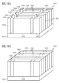
- FIG. 8C a three-dimensional view of the integrated circuit memory device 800 is shown, including both front-end-of-line (FEOL) structures, such as the gates 814 gate oxide layers 816 , and back-end-of-line (BEOL) structures, such as bit lines 804 and magnetoresistive memory elements 802 .
- FEOL front-end-of-line
- BEOL back-end-of-line
- bit lines 804 and magnetoresistive memory elements 802 bit lines 804 and magnetoresistive memory elements 802 .
- the area of a single cell 870 is outlined, and gate oxide layers 816 are shown surrounding channel portions of fin structures 872 .
- FIG. 9A shows a graph of estimated FinFET height (W eff ) in nm, against the write current in ⁇ A. As can be seen, assuming that the magnetoresistive memory element has a resistance of approximately 1 k ⁇ , and a write current of approximately 220 ⁇ A, the estimated FinFET height would be approximately 350 nm.
- FIG. 9B shows a similar graph, assuming overdrive of the FinFET. Under overdrive conditions, the gate and source/drain voltages are higher than those assumed in FIG. 9A , allowing a higher write current for the FinFET.
- a height of approximately 240 nm may be used for a magnetoresistive memory element having a resistance of approximately 2 k ⁇ , and a write current of approximately 226 ⁇ A.
- a FinFET height of approximately 240 nm to approximately 314 nm may be used in some embodiments.
- FIGS. 10A-10L show steps in the FEOL process for manufacturing an integrated circuit including a FinFET structure for use with a resistivity changing memory cell, such as is described above, in accordance with an embodiment of the invention.
- the FinFET is formed on a silicon-on-insulator (SOI) substrate.
- SOI silicon-on-insulator
- Such a process may provide a relatively high fin, permitting a relatively high drive current.
- forming the cell structure on SOI may provide effects such as a reduced capacitance for AC performance, facilitation of bidirectional bias, and a somewhat simplified process compared to, for example, formation of the FinFET on a bulk silicon substrate.
- forming the FinFET on SOI also may lead to floating body effects in some embodiments.
- FIG. 10A shows a first step in an example embodiment of an FEOL process of forming an integrated circuit including a resistivity changing memory device 1000 using FinFETs.
- trenches 1002 are formed in a silicon layer disposed above a buried oxide layer 1004 , to form elongated structures 1006 . It will be understood that the patterning and etching of the trenches 1002 in the silicon layer may be carried out using conventional lithographic and/or etching techniques.
- deep channel doping/counter doping are used to establish either p-type or n-type conductivity in the elongated structures 1006 .
- Conventional doping techniques such as ion implantation, using convention dopants, such as boron for p-type conductivity, or phosphorus, arsenic, and/or antimony for n-type conductivity, may be used, though use of other known or later discovered doping techniques and/or dopant materials also is possible.
- FIG. 10B shows the results of the next step, in which the trenches are filled with an oxide material 1008 to form isolation structures separating the elongated structures 1006 .
- the oxide material may be applied using conventional deposition techniques.
- the oxide material 1008 is then planarized, using, for example, chemical-mechanical planarization (CMP) techniques.
- CMP chemical-mechanical planarization
- a top pad oxide layer 1010 is formed.
- the top pad oxide layer may be formed by a conventional oxidation technique.
- a nitride layer 1012 may then be deposited, as shown in FIG. 10D .
- FIG. 10E shows the results of the next step, in which the nitride layer 1012 is etched according to a gate pattern, to expose portions of the device 1000 in which a gate will be formed.
- This patterning and etching may be performed, for example, using conventional lithography and etching techniques.
- the oxide has been etched from the gate pattern areas, where the nitride was removed in the previous step. This results in the formation of trenches 1014 , adjacent to the elongated structures 1006 .
- FIG. 10G shows the results of the next step, in which gate oxides 1016 have been formed around fin structures 1015 of the elongated structures 1006 in the areas of the gate patterns to form the channels for the transistors.
- the gate oxides 1016 may be formed by conventional oxidation techniques.
- the areas of the gate patterns are filled with a conductive gate material, such as doped polysilicon. Filling these areas forms gate structures 1018 that surround the fin structures 1015 and gate oxides 1016 , to complete formation of the gates for the FinFETs.
- a conductive gate material such as doped polysilicon.
- Conventional deposition techniques may be used to deposit the gate material.
- CMP techniques may be used to planarize the gate structures 1018 .
- the gate structures 1018 also serve as word lines for selecting particular memory cells for reading or writing.
- FIG. 10I shows the results of the next step, in which the nitride layer 1012 has been removed. This may be accomplished, for example, using conventional etching techniques.
- sidewall spacers 1020 are formed around a portion of the gate structures 1018 .
- the sidewall spacers 1020 are formed using conventional semiconductor processing techniques.
- the sidewall spacers 1020 may be formed by depositing an insulating material such as an oxide, nitride or oxynitride of silicon, and then using anisotropic etching to form the sidewall spacers 1020 from the deposited material.
- the sidewall spacers 1020 may be used in some embodiments for aligning contacts (not shown) and vias (not shown).
- the source regions 1022 and drain regions 1024 are doped for either n-type or p-type conductivity. If the fin structures 1015 are doped for n-type conductivity, then the source regions 1022 and drain regions 1024 may be doped for p-type conductivity. If the fin structures 1015 are doped for p-type conductivity, then the source regions 1022 and drain regions 1024 may be doped for n-type conductivity.
- the doping of the source regions 1022 and drain regions 1024 may be carried out using conventional doping techniques, such as ion implantation, using convention dopants, such as boron for p-type conductivity, or phosphorus, arsenic, and/or antimony for n-type conductivity, though other appropriate dopant materials may be used.
- conventional dopants such as boron for p-type conductivity, or phosphorus, arsenic, and/or antimony for n-type conductivity, though other appropriate dopant materials may be used.
- salicidation is used to form source contacts 1026 and drain contacts 1028 .
- other salicidation methods or methods of forming contacts for the FinFETs also may be used.
- a BEOL process in which vias, metal bit lines and common lines, and the magnetoresistive memory elements are fabricated may be used to complete the memory device. Such a BEOL process, in accordance with another embodiment of the invention, will be described in greater detail below.
- FIGS. 11A-11M show steps in the FEOL process for manufacturing a FinFET structure for use with a resistivity changing memory cell on bulk silicon, rather than on SOI.
- This embodiment may provide compatibility with other bulk technologies for memory chips.
- use of bulk silicon may involve a slightly more complex process, including two-step etches that may limit the achievable fin height in a FinFET.
- a device produced on bulk silicon may have somewhat higher junction capacitance and overlap capacitance due to bidirectional bias.
- FIG. 11A a first step in an embodiment of an FEOL process of forming a resistivity changing memory device 1100 using FinFETs is shown.
- trenches are formed in a bulk silicon layer 1102 to form elongated structures 1104 .
- the patterning and etching of the trenches in the silicon layer 1102 may be carried out using conventional lithographic and/or etching techniques.
- a channel stop implantation process is used to form a channel stop layer 1106 .
- the channel stop implantation process may employ conventional implantation techniques, using conventional dopants, such as boron for the formation of a p-type channel stop layer, or phosphorus, arsenic and/or antimony for an n-type channel stop layer.
- conventional dopants such as boron for the formation of a p-type channel stop layer, or phosphorus, arsenic and/or antimony for an n-type channel stop layer.
- the channel stop layer 1106 may be formed by other techniques, which may use other dopant materials.
- FIG. 11C shows the results of the next step, in which the trenches between the elongated structures 1104 are filled with an oxide material 1108 to form isolation structures separating the elongated structures 1104 .
- the oxide material 1108 may be applied using conventional deposition techniques.
- the oxide material 1108 may then be planarized, using, for example, chemical-mechanical planarization (CMP) techniques.
- CMP chemical-mechanical planarization
- a top pad oxide layer 1110 is formed.
- the top pad oxide layer 1110 may be formed using a conventional oxide growth technique.
- a nitride layer 1112 may then be deposited, as shown in FIG. 11E .
- FIG. 11F shows the results of the next step, in which the nitride layer 1112 is etched according to a gate pattern, to expose portions of the device 1100 in which a gate will be formed.
- This patterning and etching may be performed, for example, using conventional lithography and etching techniques.
- the oxide has been etched from the gate pattern areas where the nitride was removed in the previous step. This results in the formation of trenches 1114 , adjacent to fin structures 1115 formed from portions of the elongated structures 1104 . The fin structures 1115 will form the channel portions of the transistors. As can be seen, some of the oxide material 1108 remains in the trenches 1114 .
- channel doping/counterdoping can be carried out, in which the exposed channel areas (i.e., the fin structures 1115 ).
- Conventional doping techniques such as ion implantation, using convention dopants, such as boron for p-type conductivity, or phosphorus, arsenic, and/or antimony for n-type conductivity, may be used, though use of other known or later discovered doping techniques and/or dopant materials also is possible.
- FIG. 11H shows the results of the next step, in which gate oxides 1116 have been formed around the fin structures 1104 in the areas of the gate patterns.
- the gate oxides 1116 may be formed by conventional oxidation techniques.
- the areas of the gate patterns are filled with a conductive gate material, such as doped polysilicon. Filling these areas forms gate structures 1118 that surround the fin structures 1115 and gate oxides 1116 , to complete formation of the gates for the FinFETs.
- a conductive gate material such as doped polysilicon.
- Conventional deposition techniques may be used to deposit the gate material.
- CMP techniques may be used to planarize the gate structures 1118 .
- the gate structures 1118 also serve as word lines for selecting particular memory cells for reading or writing.
- FIG. 11J shows the results of the next step, in which the nitride layer 1112 has been removed. This may be accomplished, for example, using conventional etching techniques.
- sidewall spacers 1120 are formed around a portion of the gate structures 1118 .
- the sidewall spacers 1120 are formed using conventional semiconductor processing techniques.
- the sidewall spacers 1120 may be formed by depositing an insulating material such as an oxide, nitride or oxynitride of silicon, and then using etching to form the sidewall spacers 1120 from the deposited material.
- the sidewall spacers 1120 may be used in some embodiments for aligning contacts (not shown) and vias (not shown).
- the source regions 1122 and drain regions 1124 are doped for either n-type or p-type conductivity. If the portions of the fin structures 1115 that are surrounded by the gate oxides 1116 and gate structures 1118 are doped for n-type conductivity, then the source regions 1122 and drain regions 1124 may be doped for p-type conductivity. If the portions of the fin structures 1115 that are surrounded by the gate oxides 1116 and gate structures 1118 are doped for p-type conductivity, then the source regions 1122 and drain regions 1124 may be doped for n-type conductivity.
- the doping of the source regions 1122 and drain regions 1124 may be carried out using conventional doping techniques, such as ion implantation, using convention dopants, such as boron for p-type conductivity, or phosphorus, arsenic, and/or antimony for n-type conductivity, though other appropriate dopant materials may be used.
- conventional dopants such as boron for p-type conductivity, or phosphorus, arsenic, and/or antimony for n-type conductivity, though other appropriate dopant materials may be used.
- a salicidation process is used to form source contacts 1126 and drain contacts 1128 .
- This generally involves depositing a metal over the areas of silicon where the contacts are to be formed, and then reacting the metal with the silicon to form a silicide at a high temperature, during an anneal or sinter process.
- other salicidation methods or methods of forming contacts for the FinFETs also may be used.
- a BEOL process similar to that illustrated below, in which vias, metal bit lines and common lines, and the magnetoresistive memory elements are fabricated may be used to complete the memory device.
- the amount of current that can be driven by a single FinFET may not be sufficient for switching some types of high-current memory technologies, such as some types of resistivity changing memories.
- some types of MRAM, PCRAM, and carbon memory devices may require high switching currents that may be difficult to drive with a single FinFET.
- two or more FinFETs may be used to drive the needed switching current.
- some such embodiments may have a cell size below 10 F 2 , permitting memory devices to be constructed that have densities similar to those that may be achieved using low switching current technologies, such as DRAM.
- FIGS. 12A-C show an embodiment of an integrated circuit MRAM device in which two FinFETs are used to drive the switching current.
- a cell 1202 of the integrated circuit memory device 1200 includes a magnetoresistive memory elements 1204 , connected through a source via 1242 and a source contact 1244 between a bit line 1206 and a source region 1208 of a first FinFET 1210 and a second FinFET 1212 .
- a first drain region 1214 is shared by an adjacent FinFET, and is electrically connected through a first drain contact 1216 a first drain via 1218 to a first common line 1220 , which may be connected to ground.
- a second drain region 1222 (which is also shared by an adjacent FinFET) is electrically connected through a second drain contact 1224 and a second drain via 1226 to a second common line 1228 , which may be connected to ground.
- a first gate 1230 and a second gate 1232 also serve as word lines, and surround a first gate oxide layer 1234 and a second gate oxide layer 1236 of the first FinFET 1210 and the second FinFET 1212 , respectively.
- additional lines 1238 including spacers 1240 are used for aligning the source via 1242 and the first and second drain vias 1218 and 1226 .
- the first FinFET 1210 and second FinFET 1212 are formed in a substrate 1246 .
- both the first gate 1230 and the second gate 1232 are activated (using the word lines associated with the gates), permitting current to be driven through both the first FinFET 1210 and the second FinFET 1212 . It is noted that the drain regions 1214 and 1222 are shared with other neighboring FinFETs that belong to other adjacent memory cells. This concept will be used throughout below without further indication.
- FIG. 12B shows a layout of memory cells in the integrated circuit memory device 1200 , in accordance with an embodiment of the invention.
- the length of the cell 1202 includes half of the length of the shared first and second drain regions 1214 and 1222 , the length of the source region 1208 , and the width of the first and second gates 1230 and 1232 .
- the width of the cell 1202 includes the width of the active areas of the cell 1202 , as well as the width (half on either side of the cell 1202 ) of an isolation region 1252 .
- the width of the transistor is no longer limiting on the current that the transistor can drive, so the width of the cell may depend on other factors, such as the contact width and minimum feature size. Accordingly, the width of the cell shown in FIG. 8B , W cell , may be approximately 130 nm, while the length of the cell, L cell , may be approximately 320 nm. With a node size of 65 nm, this means that the cell has a width of approximately 2 F, and a length of approximately 4.92 F, giving an area of approximately 9.84 F 2 , which is below the 10 F 2 area that is needed to provide a density that is competitive with many other memory technologies, such as DRAM.
- FIG. 12C a three-dimensional view of the integrated circuit memory device 1200 is shown, including both FEOL and BEOL structures. In this view, the area of a single cell 1270 is outlined. Arrows in the image show the flow of current through the two FinFETs of the cell 1270 .
- FIGS. 13A-13I a BEOL process for manufacturing a memory device using two FinFETs, in accordance with an embodiment of the invention.
- the resistivity changing memory device is an MRAM device. It will, however, be understood that a similar process could be used for the manufacture of other memory devices, including resistivity changing memory devices, that may use a relatively high switching current.
- FIG. 13A shows a partially manufactured memory device 1300 at the start of the BEOL process.
- the memory device 1300 already includes FinFETs 1302 and 1304 , including a source region 1306 , a source contact 1308 , a first drain region 1310 , a first drain contact 1312 , a second drain region 1314 , a second drain contact 1316 , a first gate 1318 , and a second gate 1319 , all formed on a substrate 1301 (bulk silicon in this embodiment, though SOI or other types of substrate are also possible).
- the first gate 1318 and second gate 1319 also serve as word lines.
- FIG. 13B shows the next step in the process of manufacturing the memory device 1300 .
- extra lines 1320 are formed.
- the extra lines 1320 may be used only for the purpose of forming self-aligned vias in a subsequent step, while in other embodiments, the extra lines 1320 may be used for carrying electrical signals.
- sidewall spacers 1322 are formed around the extra lines 1320 .
- these sidewall spacers 1322 will be used for forming self-aligned vias in a subsequent step.
- the sidewall spacers 1322 may be formed by depositing an insulating material such as an oxide, nitride or oxynitride of silicon, and then using etching to form the sidewall spacers 1322 from the deposited material.
- the sidewall spacers may be formed from an insulating material different than the dielectric material deposited in the previous step, so that the sidewall spacers may be etched without having a substantial effect on the underlying dielectric material.
- FIG. 13D shows a next step, in which an inter-layer dielectric (ILD) material (not shown) is deposited and, in some embodiments, planarized.
- ILD inter-layer dielectric
- Conventional deposition techniques such as chemical vapor deposition (CVD)
- CVD chemical vapor deposition
- CMP planarization techniques
- Deep vias including a source via 1324 and drain vias 1326 are formed in alignment with the source contact 1308 , and the first and second drain contacts 1312 and 1316 . Holes for these vias may be formed by conventional lithographic and etching techniques. In some embodiments, the extra lines 1320 and spacers 1322 are used to align the vias. The vias are then filled with a conductive material, such as a metal material, and planarized. This may be accomplished using conventional deposition and planarization techniques. In some embodiments, filling the vias is done as part of the metallization step described below with reference to FIG. 13E .
- an M1 metallization layer is formed, including common lines 1330 .
- the common lines 1330 may be formed of a conductive material, such as a metal material, and are electrically connected to the drain vias 1326 . In some embodiments, the common lines 1330 may be electrically connected to ground.
- the conductive material may be deposited using conventional deposition techniques, and patterned using, for example, conventional lithographic and etching techniques.
- FIG. 13F a next step is shown, in which a further layer of an ILD material (not shown) is deposited and, in some embodiments, planarized.
- a further layer of an ILD material (not shown) is deposited and, in some embodiments, planarized.
- Conventional deposition techniques, such as CVD, and conventional planarization techniques, such as CMP may be used to deposit and planarize the ILD material, though other techniques may be used.
- a second via 1332 is formed in the layer of ILD material, aligned with and electrically connected to the source via 1324 .
- a hole for the second via 1332 may be formed by conventional lithographic and etching techniques.
- the second via 1332 may be filled with a conductive material, such as a metal material, and planarized. This may be accomplished using conventional deposition and planarization techniques. In some embodiments, filling the second via 1332 may be part of the step of forming the memory element connector, as described below with reference to FIG. 13G .
- a memory element connector 1334 is formed.
- the memory element bottom connector 1334 is formed of a conductive material, such as a metal, and is electrically connected to the second via 1332 .
- the memory element connector 1334 may be formed by depositing and patterning the conductive material using conventional techniques.
- FIG. 13H shows a next step, in which a memory element 1336 , such as a resistivity changing memory element is formed.
- the memory element 1336 includes a magnetoresistive memory element, though other types of memory elements may be used.
- a magnetoresistive memory element numerous magnetic metal layers of materials such as PtMn, CoFe, Ru, and NiFe may be deposited to form a free layer (not shown) and a fixed layer (not shown).
- a tunnel layer (not shown), including a dielectric material such as MgO or Al 2 O 3 may be formed between the free layer and the fixed layer.
- materials for ohmic heating may be deposited for use in a thermal select magnetoresistive memory element. It will be understood that other methods of forming a magnetoresistive memory element, a resistivity changing memory element, or other high switching current memory element may be used in accordance with various embodiments of the invention.
- bit line 1338 is formed in an M2 metallization layer.
- the bit line 1338 is formed of a conductive material, such as a metal material.
- the conductive material may be deposited using conventional deposition techniques, and patterned using, for example, conventional lithographic and etching techniques.
- an additional top contact electrode (not shown) is used to provide an electrical contact between the bit line 1338 and memory element 1336 .
- Formation of the bit line 1338 completes the formation of the memory device 1300 , though in some embodiments, additional layers and devices may be formed on an integrated circuit above the memory device 1300 . It will be understood that the BEOL process described with reference to FIGS. 13A-13I could be used, with slight modifications, with the single FinFET embodiments shown above in FIGS. 10A-10L and FIGS. 11A-11M , or with other single or multi FinFET embodiments of the invention.
- Memory cells formed using a FinFET in accordance with an embodiment of the invention may be used in memory devices that contain large numbers of such cells. These cells may, for example, be organized into an array of memory cells having numerous rows and columns of cells, each of which stores more than one bit of information. Memory devices of this sort may be used in a variety of applications or systems. As shown in FIGS. 14A and 14B , in some embodiments, memory devices such as those described herein may be used in modules. In FIG. 14A , a memory module 1400 is shown, on which one or more memory devices 1404 are arranged on a substrate 1402 . Each memory device 1404 may include numerous memory cells in accordance with an embodiment of the invention.
- the memory module 1400 may also include one or more electronic devices 1406 , which may include memory, processing circuitry, control circuitry, addressing circuitry, bus interconnection circuitry, or other circuitry or electronic devices that may be combined on a module with a memory device 1404 . Additionally, the memory module 1400 includes multiple electrical connections 1408 , which may be used to connect the memory module 1400 to other electronic components, including other modules. For example, the memory module 1400 may be plugged into a larger circuit board, including PC main boards, video adapters, cell phone circuit boards or portable video or audio players, among others.
- a stackable memory module 1452 may include one or more memory devices 1456 , arranged on a stackable substrate 1454 . Each of the memory devices 1456 includes memory cells that employ memory elements in accordance with an embodiment of the invention.
- the stackable memory module 1452 also may include one or more electronic devices 1458 , which may include memory, processing circuitry, control circuitry, addressing circuitry, bus interconnection circuitry, or other circuitry or electronic devices that may be combined on a module with a memory device 1456 .
- Electrical connections 1460 are used to connect the stackable memory module 1452 with other modules in the stack 1450 , or with other electronic devices.
- Other modules in the stack 1450 may include additional stackable memory modules, similar to the stackable memory module 1452 described above, or other types of stackable modules, such as stackable processing modules, control modules, communication modules, or other modules containing electronic components.
- one embodiment provides an integrated circuit including a memory cell including a resistivity changing memory element and a first select transistor electrically coupled to the resistivity changing memory element, wherein the first select transistor includes a FinFET including a source, a drain, and a fin structure formed above a surface of a substrate between the source and the drain.
- the fin structure includes a channel area extending in a direction substantially parallel to the surface of the substrate, wherein a dielectric layer is formed around at least a portion of the channel area such that an effective channel width of the first select transistor depends at least in part on a height of the fin structure.
- a maximum switching current of the resistivity changing memory element depends at least in part on the height of the fin structure.
- the substrate includes a silicon-on-insulator substrate. In other embodiments, the substrate includes a bulk silicon substrate.
- the resistivity changing memory element includes a magnetoresistive memory element.
- the magnetoresistive memory element is positioned to decrease magnetic interaction with magnetoresistive memory elements of adjacent memory cells.
- the resistivity changing memory element includes a phase changing memory element. In some embodiments, the resistivity changing memory element includes a carbon memory element. In some embodiments, the resistivity changing memory element includes a conductive bridging memory element.
- the memory cell has an area less than 10 F 2 , where F is the minimum feature size on the integrated circuit.
- the memory cell further includes a second select transistor electrically coupled to the resistivity changing memory element, the second select transistor including a FinFET.
- the first select transistor and the second select transistor share one of the source and the drain.
- a maximum switching current for the resistivity changing memory element depends on a maximum current driven by the first select transistor and a maximum current driven by the second select transistor.
- a method of manufacturing an integrated circuit including providing a substrate; forming a first FinFET above a surface of the substrate, the first FinFET including a source, a drain, and a fin structure disposed between the source and the drain, the fin structure including a channel area extending in a direction substantially parallel to the surface of the substrate, wherein a dielectric layer is formed around at least a portion of the channel area such that an effective channel width of the first FinFET depends at least in part on a height of the fin structure; and forming a resistivity changing memory element electrically coupled to the first FinFET.
- the method further includes depositing a first dielectric material above the substrate; forming first and second lines above the dielectric material; forming sidewall spacers adjacent to the first and second lines; and using the sidewall spacers to align a via with at least one of the source region and the drain region.
- forming sidewall spacers includes depositing a second dielectric material, different from the first dielectric material, and etching the second dielectric material to form the sidewall spacers.
- forming the first FinFET includes etching a trench to define an elongated structure; doping a first portion of the elongated structure to form the source; doping a second portion of the elongated structure to form the drain, such that the remaining portion of the elongated structure forms the fin structure extending between the source and the drain to form the channel area; forming the dielectric layer around at least a portion of the channel area; and depositing a conductive material in at least a portion of the trench surrounding the dielectric layer to form a gate.
- providing a substrate includes providing a silicon on insulator substrate. In other embodiments, providing a substrate includes providing a bulk silicon substrate.
- the method further includes forming a second FinFET above the surface of the substrate, the second FinFET electrically coupled to the resistivity changing memory element.
- forming the second FinFET includes forming the second FinFET such that the Second FinFET shares one of the source and the drain with the first FinFET.
- forming a resistivity changing memory element includes forming a magnetoresistive memory element. In some of these embodiments, forming a magnetoresistive memory element includes positioning the magnetoresistive memory element in an asymmetric pattern with respect to adjacent magnetoresistive memory elements to decrease magnetic interaction with said adjacent magnetoresistive memory elements.
- forming a resistivity changing memory element includes forming a phase changing memory element. In some embodiments, forming a resistivity changing memory element includes forming a carbon memory element. In some embodiments, forming a resistivity changing memory element includes forming a conductive bridging memory element. In some embodiments, forming a resistivity changing memory element includes forming a transition metal oxide memory element.
- the first select transistor includes a FinFET including a first source/drain area, a second source/drain area, and a fin structure formed above a surface of the substrate between the first source/drain area and the second source/drain area.
- the fin structure includes a channel area extending in a direction substantially parallel to the surface of the substrate, wherein a dielectric layer is formed around at least a portion of the channel area such that an effective channel width of the first select transistor depends at least in part on a height of the fin structure, and a gate formed surrounding the dielectric layer, the gate controlling a flow of current through the channel area.
- the integrated circuit further includes a bit line electrically coupled to the first source/drain area of the first select transistor, a word line electrically coupled to the gate of the first select transistor, and a common line electrically coupled to the second source/drain area of the first select transistor.
- the bit line is electrically coupled to the first source/drain area of the first select transistor through a self-aligned via.
- the common line is electrically coupled to the second source/drain area of the first select transistor through a self-aligned via.
- the integrated circuit further includes an extra line surrounded by sidewall spacers, the extra line and sidewall spacers used for alignment of a self-aligned via.
- a maximum switching current of the resistivity changing memory element depends at least in part on the height of the fin structure.
- the substrate includes a silicon-on-insulator substrate. In other embodiments, the substrate includes a bulk silicon substrate.
- the resistivity changing memory element includes one of a magnetoresistive memory element, a phase changing memory element, a carbon memory element, and a conductive bridging memory element.
- the integrated circuit further includes a second select transistor electrically coupled to the resistivity changing memory element, the second select transistor including a FinFET.
- a maximum switching current for the resistivity changing memory element depends on a maximum current driven by the first select transistor and a maximum current driven by the second select transistor.
- Another embodiment of the invention provides a method of manufacturing an integrated circuit, including providing a substrate, and performing a front-end-of-line (FEOL) process in which a first FinFET is formed above a surface of the substrate.
- the first FinFET includes a source, a drain, and a fin structure disposed between the source and the drain, the fin structure including a channel area extending in a direction substantially parallel to the surface of the substrate.
- a dielectric layer is formed around at least a portion of the channel area such that an effective channel width of the first FinFET depends at least in part on a height of the fin structure.
- the method further includes performing a back-end-of-line (BEOL) process in which a resistivity changing memory element is formed, the resistivity changing memory element electrically coupled to the first FinFET.
- BEOL back-end-of-line
- performing a FEOL process further includes forming a second FinFET above the surface of the substrate.
- forming the second FinFET includes forming the second FinFET such that the Second FinFET shares one of the source and the drain with the first FinFET.
- performing a BEOL process further includes forming a via that electrically connects the second FinFET to the resistivity changing memory device.
- performing a FEOL process includes etching a trench to define an elongated structure; doping a first portion of the elongated structure to form the source; doping a second portion of the elongated structure to form the drain, such that the remaining portion of the elongated structure forms the fin structure extending between the source and the drain to form the channel area; forming the dielectric layer around at least a portion of the channel area; and depositing a conductive material in at least a portion of the trench surrounding the dielectric layer to form a gate.
- performing a BEOL process includes depositing a first dielectric material above the substrate; forming first and second lines above the dielectric material; forming sidewall spacers adjacent to the first and second lines; and using the sidewall spacers to align a via with at least one of the source region and the drain region.
- performing a back-end-of-line (BEOL) process in which a resistivity changing memory element is formed includes forming one of a magnetoresistive memory element, a phase changing memory element, a carbon memory element, a conductive bridging memory element, and a transition metal oxide memory element.
- an integrated circuit including resistivity changing memory means for storing information using a change in resistivity of the resistivity changing memory means; and a first select transistor electrically coupled to the resistivity changing memory means, wherein the first select transistor includes a FinFET including a source, a drain, and a fin structure formed above a surface of a substrate between the source and the drain, the fin structure including a channel area extending in a direction substantially parallel to the surface of the substrate, wherein a dielectric layer is formed around at least a portion of the channel area such that an effective channel width of the first select transistor depends at least in part on a height of the fin structure.
- the integrated circuit further includes a second select transistor electrically coupled to the resistivity changing memory means, the second select transistor including a FinFET.
- a memory module including a plurality of integrated circuits, wherein the integrated circuits include a memory cell including a resistivity changing memory element and a first select transistor electrically coupled to the resistivity changing memory element.
- the first select transistor includes a FinFET including a source, a drain, and a fin structure formed above a surface of a substrate between the source and the drain, the fin structure including a channel area extending in a direction substantially parallel to the surface of the substrate.
- a dielectric layer is formed around at least a portion of the channel area such that an effective channel width of the first select transistor depends at least in part on a height of the fin structure.
- a maximum switching current of the resistivity changing memory element depends at least in part on the height of the fin structure.
- the memory cell has an area less than 10 F 2 , where F is the minimum feature size on the integrated circuit.
- the memory cell further includes a second select transistor electrically coupled to the resistivity changing memory element, the second select transistor including a FinFET.
- the resistivity changing memory element includes one of a magnetoresistive memory element, a phase changing memory element, a carbon memory element, a conductive bridging memory element, and a transition metal oxide memory element.
- the memory module is stackable.
Abstract
Description
Claims (14)
Priority Applications (2)
| Application Number | Priority Date | Filing Date | Title |
|---|---|---|---|
| US11/864,575 US8665629B2 (en) | 2007-09-28 | 2007-09-28 | Condensed memory cell structure using a FinFET |
| EP08015079.0A EP2043156B1 (en) | 2007-09-28 | 2008-08-27 | Condensed memory cell structure using a FinFET |
Applications Claiming Priority (1)
| Application Number | Priority Date | Filing Date | Title |
|---|---|---|---|
| US11/864,575 US8665629B2 (en) | 2007-09-28 | 2007-09-28 | Condensed memory cell structure using a FinFET |
Publications (2)
| Publication Number | Publication Date |
|---|---|
| US20090085121A1 US20090085121A1 (en) | 2009-04-02 |
| US8665629B2 true US8665629B2 (en) | 2014-03-04 |
Family
ID=40193863
Family Applications (1)
| Application Number | Title | Priority Date | Filing Date |
|---|---|---|---|
| US11/864,575 Active 2031-12-13 US8665629B2 (en) | 2007-09-28 | 2007-09-28 | Condensed memory cell structure using a FinFET |
Country Status (2)
| Country | Link |
|---|---|
| US (1) | US8665629B2 (en) |
| EP (1) | EP2043156B1 (en) |
Cited By (12)
| Publication number | Priority date | Publication date | Assignee | Title |
|---|---|---|---|---|
| US20140043894A1 (en) * | 2012-08-09 | 2014-02-13 | Micron Technology, Inc. | Memory cells having a plurality of resistance variable materials |
| US20140353801A1 (en) * | 2013-05-31 | 2014-12-04 | Globalfoundries Inc. | Device isolation in finfet cmos |
| US20150028425A1 (en) * | 2013-07-26 | 2015-01-29 | SK Hynix Inc. | Three dimensional semiconductor device having lateral channel and method of manufacturing the same |
| US9123575B1 (en) * | 2014-07-21 | 2015-09-01 | Avalanche Technology, Inc. | Semiconductor memory device having increased separation between memory elements |
| US9418994B1 (en) * | 2015-03-26 | 2016-08-16 | Taiwan Semiconductor Manufacturing Co., Ltd | Fin field effect transistor (FinFET) device structure |
| US9548448B1 (en) * | 2015-11-12 | 2017-01-17 | Avalanche Technology, Inc. | Memory device with increased separation between memory elements |
| US9601567B1 (en) * | 2015-10-30 | 2017-03-21 | Taiwan Semiconductor Manufacturing Co., Ltd. | Multiple Fin FET structures having an insulating separation plug |
| US10312149B1 (en) | 2015-03-26 | 2019-06-04 | Taiwan Semiconductor Manufacturing Co., Ltd | Fin field effect transistor (FinFET) device structure and method for forming the same |
| US10553643B2 (en) * | 2018-06-28 | 2020-02-04 | Microsemi Soc Corp. | Circuit and layout for resistive random-access memory arrays having two bit lines per column |
| US10553646B2 (en) * | 2018-06-28 | 2020-02-04 | Microsemi Soc Corp. | Circuit and layout for resistive random-access memory arrays |
| US10622407B1 (en) | 2019-07-15 | 2020-04-14 | United Microelectronics Corp. | Magnetic memory cell and fabrication method thereof |
| US10840447B2 (en) | 2019-03-12 | 2020-11-17 | International Business Machines Corporation | Fabrication of phase change memory cell in integrated circuit |
Families Citing this family (39)
| Publication number | Priority date | Publication date | Assignee | Title |
|---|---|---|---|---|
| US20060250918A1 (en) | 2005-05-06 | 2006-11-09 | Chih-Chin Hsu | High frequency modulation of a light beam in optical recording |
| US7768812B2 (en) | 2008-01-15 | 2010-08-03 | Micron Technology, Inc. | Memory cells, memory cell programming methods, memory cell reading methods, memory cell operating methods, and memory devices |
| US8034655B2 (en) | 2008-04-08 | 2011-10-11 | Micron Technology, Inc. | Non-volatile resistive oxide memory cells, non-volatile resistive oxide memory arrays, and methods of forming non-volatile resistive oxide memory cells and memory arrays |
| US7723180B2 (en) | 2008-04-11 | 2010-05-25 | Sandisk 3D Llc | Multilevel nonvolatile memory device containing a carbon storage material and methods of making and using same |
| US7830698B2 (en) | 2008-04-11 | 2010-11-09 | Sandisk 3D Llc | Multilevel nonvolatile memory device containing a carbon storage material and methods of making and using same |
| US7859887B2 (en) | 2008-04-11 | 2010-12-28 | Sandisk 3D Llc | Multilevel nonvolatile memory device containing a carbon storage material and methods of making and using same |
| US7812335B2 (en) | 2008-04-11 | 2010-10-12 | Sandisk 3D Llc | Sidewall structured switchable resistor cell |
| US8048474B2 (en) | 2008-04-11 | 2011-11-01 | Sandisk 3D Llc | Method of making nonvolatile memory cell containing carbon resistivity switching as a storage element by low temperature processing |
| WO2009126489A1 (en) * | 2008-04-11 | 2009-10-15 | Sandisk 3D Llc | Multilevel nonvolatile memory device containing a carbon storage material and methods of making and using same |
| US8211743B2 (en) | 2008-05-02 | 2012-07-03 | Micron Technology, Inc. | Methods of forming non-volatile memory cells having multi-resistive state material between conductive electrodes |
| US8134137B2 (en) | 2008-06-18 | 2012-03-13 | Micron Technology, Inc. | Memory device constructions, memory cell forming methods, and semiconductor construction forming methods |
| US9343665B2 (en) * | 2008-07-02 | 2016-05-17 | Micron Technology, Inc. | Methods of forming a non-volatile resistive oxide memory cell and methods of forming a non-volatile resistive oxide memory array |
| JP2010040630A (en) * | 2008-08-01 | 2010-02-18 | Toshiba Corp | Semiconductor device |
| KR101052875B1 (en) * | 2008-12-30 | 2011-07-29 | 주식회사 하이닉스반도체 | Method of manufacturing resistive RAM device |
| US8350316B2 (en) * | 2009-05-22 | 2013-01-08 | Macronix International Co., Ltd. | Phase change memory cells having vertical channel access transistor and memory plane |
| US8427859B2 (en) | 2010-04-22 | 2013-04-23 | Micron Technology, Inc. | Arrays of vertically stacked tiers of non-volatile cross point memory cells, methods of forming arrays of vertically stacked tiers of non-volatile cross point memory cells, and methods of reading a data value stored by an array of vertically stacked tiers of non-volatile cross point memory cells |
| US8411477B2 (en) | 2010-04-22 | 2013-04-02 | Micron Technology, Inc. | Arrays of vertically stacked tiers of non-volatile cross point memory cells, methods of forming arrays of vertically stacked tiers of non-volatile cross point memory cells, and methods of reading a data value stored by an array of vertically stacked tiers of non-volatile cross point memory cells |
| US8289763B2 (en) | 2010-06-07 | 2012-10-16 | Micron Technology, Inc. | Memory arrays |
| US8351242B2 (en) | 2010-09-29 | 2013-01-08 | Micron Technology, Inc. | Electronic devices, memory devices and memory arrays |
| US8759809B2 (en) | 2010-10-21 | 2014-06-24 | Micron Technology, Inc. | Integrated circuitry comprising nonvolatile memory cells having platelike electrode and ion conductive material layer |
| US8526213B2 (en) | 2010-11-01 | 2013-09-03 | Micron Technology, Inc. | Memory cells, methods of programming memory cells, and methods of forming memory cells |
| US8796661B2 (en) | 2010-11-01 | 2014-08-05 | Micron Technology, Inc. | Nonvolatile memory cells and methods of forming nonvolatile memory cell |
| US9454997B2 (en) | 2010-12-02 | 2016-09-27 | Micron Technology, Inc. | Array of nonvolatile memory cells having at least five memory cells per unit cell, having a plurality of the unit cells which individually comprise three elevational regions of programmable material, and/or having a continuous volume having a combination of a plurality of vertically oriented memory cells and a plurality of horizontally oriented memory cells; array of vertically stacked tiers of nonvolatile memory cells |
| US8431458B2 (en) | 2010-12-27 | 2013-04-30 | Micron Technology, Inc. | Methods of forming a nonvolatile memory cell and methods of forming an array of nonvolatile memory cells |
| JP5426581B2 (en) | 2011-01-14 | 2014-02-26 | 株式会社東芝 | Semiconductor memory device |
| US8791447B2 (en) | 2011-01-20 | 2014-07-29 | Micron Technology, Inc. | Arrays of nonvolatile memory cells and methods of forming arrays of nonvolatile memory cells |
| US8488365B2 (en) | 2011-02-24 | 2013-07-16 | Micron Technology, Inc. | Memory cells |
| US8537592B2 (en) | 2011-04-15 | 2013-09-17 | Micron Technology, Inc. | Arrays of nonvolatile memory cells and methods of forming arrays of nonvolatile memory cells |
| US8664729B2 (en) * | 2011-12-14 | 2014-03-04 | Taiwan Semiconductor Manufacturing Company, Ltd. | Methods and apparatus for reduced gate resistance finFET |
| EP2608210B1 (en) | 2011-12-23 | 2019-04-17 | IMEC vzw | Stacked RRAM array with integrated transistor selector |
| US9702763B2 (en) * | 2013-06-17 | 2017-07-11 | Taiwan Semiconductor Manufacturing Company, Ltd. | Thermal sensor |
| KR102072410B1 (en) | 2013-08-07 | 2020-02-03 | 삼성전자 주식회사 | Semiconductor device and fabricated method thereof |
| US9601495B2 (en) * | 2015-07-30 | 2017-03-21 | Globalfoundries Inc. | Three-dimensional semiconductor device with co-fabricated adjacent capacitor |
| US10181496B1 (en) * | 2016-04-29 | 2019-01-15 | Adesto Technologies Corporation | Programmable impedance memory device and related methods |
| CN108075038A (en) * | 2016-11-11 | 2018-05-25 | 中芯国际集成电路制造(上海)有限公司 | Dynamic RAM and forming method thereof |
| US11011517B2 (en) | 2019-01-02 | 2021-05-18 | International Business Machines Corporation | Semiconductor structure including first FinFET devices for low power applications and second FinFET devices for high power applications |
| CN111834364B (en) * | 2019-04-19 | 2023-08-29 | 华邦电子股份有限公司 | Dynamic random access memory |
| US11121174B2 (en) * | 2019-11-21 | 2021-09-14 | International Business Machines Corporation | MRAM integration into the MOL for fast 1T1M cells |
| US11568121B2 (en) * | 2020-06-19 | 2023-01-31 | Taiwan Semiconductor Manufacturing Company, Ltd. | FinFET semiconductor device grouping |
Citations (14)
| Publication number | Priority date | Publication date | Assignee | Title |
|---|---|---|---|---|
| US5640343A (en) * | 1996-03-18 | 1997-06-17 | International Business Machines Corporation | Magnetic memory array using magnetic tunnel junction devices in the memory cells |
| US6097625A (en) * | 1998-07-16 | 2000-08-01 | International Business Machines Corporation | Magnetic random access memory (MRAM) array with magnetic tunnel junction (MTJ) cells and remote diodes |
| US6940747B1 (en) * | 2004-05-26 | 2005-09-06 | Hewlett-Packard Development Company, L.P. | Magnetic memory device |
| US7002195B2 (en) * | 2003-05-13 | 2006-02-21 | Samsung Electronics Co., Ltd. | Magnetic random access memory (MRAM) cells having split sub-digit lines |
| US20060067112A1 (en) * | 2004-09-30 | 2006-03-30 | Richard Ferrant | Resistive memory cell random access memory device and method of fabrication |
| US20060077737A1 (en) * | 2004-07-14 | 2006-04-13 | Renesas Technology Corp. | Non-volatile semiconductor memory device |
| US7309885B2 (en) * | 2004-10-08 | 2007-12-18 | Samsung Electronics Co., Ltd. | PRAMs having a plurality of active regions located vertically in sequence and methods of forming the same |
| US7345899B2 (en) * | 2006-04-07 | 2008-03-18 | Infineon Technologies Ag | Memory having storage locations within a common volume of phase change material |
| US7397689B2 (en) * | 2006-08-09 | 2008-07-08 | Micron Technology, Inc. | Resistive memory device |
| US7474555B2 (en) * | 2006-03-17 | 2009-01-06 | Thomas Nirschl | Integrated circuit including resistivity changing material element |
| US20090014706A1 (en) * | 2007-07-13 | 2009-01-15 | Macronix International Co., Ltd. | 4f2 self align fin bottom electrodes fet drive phase change memory |
| US7606055B2 (en) * | 2006-05-18 | 2009-10-20 | Micron Technology, Inc. | Memory architecture and cell design employing two access transistors |
| US7723786B2 (en) * | 2007-04-11 | 2010-05-25 | Ronald Kakoschke | Apparatus of memory array using FinFETs |
| US20130148409A1 (en) * | 2011-02-14 | 2013-06-13 | Shine C. Chung | Circuit and system of using finfet for building programmable resistive devices |
Family Cites Families (3)
| Publication number | Priority date | Publication date | Assignee | Title |
|---|---|---|---|---|
| JP2005277189A (en) * | 2004-03-25 | 2005-10-06 | Renesas Technology Corp | Magnetic storage device |
| TWI295506B (en) * | 2005-02-03 | 2008-04-01 | Samsung Electronics Co Ltd | Semiconductor device having transistor with vertical gate electrode and method of fabricating the same |
| KR100657964B1 (en) * | 2005-07-22 | 2006-12-14 | 삼성전자주식회사 | Semiconductor device and random access memory having a single gate electrode corresponding a pair of fin-type channel regions |
-
2007
- 2007-09-28 US US11/864,575 patent/US8665629B2/en active Active
-
2008
- 2008-08-27 EP EP08015079.0A patent/EP2043156B1/en active Active
Patent Citations (16)
| Publication number | Priority date | Publication date | Assignee | Title |
|---|---|---|---|---|
| US5640343A (en) * | 1996-03-18 | 1997-06-17 | International Business Machines Corporation | Magnetic memory array using magnetic tunnel junction devices in the memory cells |
| US6097625A (en) * | 1998-07-16 | 2000-08-01 | International Business Machines Corporation | Magnetic random access memory (MRAM) array with magnetic tunnel junction (MTJ) cells and remote diodes |
| US7002195B2 (en) * | 2003-05-13 | 2006-02-21 | Samsung Electronics Co., Ltd. | Magnetic random access memory (MRAM) cells having split sub-digit lines |
| US6940747B1 (en) * | 2004-05-26 | 2005-09-06 | Hewlett-Packard Development Company, L.P. | Magnetic memory device |
| US20060077737A1 (en) * | 2004-07-14 | 2006-04-13 | Renesas Technology Corp. | Non-volatile semiconductor memory device |
| US7286394B2 (en) * | 2004-07-14 | 2007-10-23 | Renesas Technology Corp. | Non-volatile semiconductor memory device allowing concurrent data writing and data reading |
| US20060067112A1 (en) * | 2004-09-30 | 2006-03-30 | Richard Ferrant | Resistive memory cell random access memory device and method of fabrication |
| US7212432B2 (en) | 2004-09-30 | 2007-05-01 | Infineon Technologies Ag | Resistive memory cell random access memory device and method of fabrication |
| US7309885B2 (en) * | 2004-10-08 | 2007-12-18 | Samsung Electronics Co., Ltd. | PRAMs having a plurality of active regions located vertically in sequence and methods of forming the same |
| US7474555B2 (en) * | 2006-03-17 | 2009-01-06 | Thomas Nirschl | Integrated circuit including resistivity changing material element |
| US7345899B2 (en) * | 2006-04-07 | 2008-03-18 | Infineon Technologies Ag | Memory having storage locations within a common volume of phase change material |
| US7606055B2 (en) * | 2006-05-18 | 2009-10-20 | Micron Technology, Inc. | Memory architecture and cell design employing two access transistors |
| US7397689B2 (en) * | 2006-08-09 | 2008-07-08 | Micron Technology, Inc. | Resistive memory device |
| US7723786B2 (en) * | 2007-04-11 | 2010-05-25 | Ronald Kakoschke | Apparatus of memory array using FinFETs |
| US20090014706A1 (en) * | 2007-07-13 | 2009-01-15 | Macronix International Co., Ltd. | 4f2 self align fin bottom electrodes fet drive phase change memory |
| US20130148409A1 (en) * | 2011-02-14 | 2013-06-13 | Shine C. Chung | Circuit and system of using finfet for building programmable resistive devices |
Cited By (22)
| Publication number | Priority date | Publication date | Assignee | Title |
|---|---|---|---|---|
| US9679641B2 (en) | 2012-08-09 | 2017-06-13 | Micron Technology, Inc. | Memory cells having a plurality of resistance variable materials |
| US8964448B2 (en) * | 2012-08-09 | 2015-02-24 | Micron Technology, Inc. | Memory cells having a plurality of resistance variable materials |
| US20140043894A1 (en) * | 2012-08-09 | 2014-02-13 | Micron Technology, Inc. | Memory cells having a plurality of resistance variable materials |
| US10460798B2 (en) | 2012-08-09 | 2019-10-29 | Micron Technology, Inc. | Memory cells having a plurality of resistance variable materials |
| US9449683B2 (en) | 2012-08-09 | 2016-09-20 | Micron Technology, Inc. | Memory cells having a plurality of resistance variable materials |
| US10102905B2 (en) | 2012-08-09 | 2018-10-16 | Micron Technology, Inc. | Memory cells having a plurality of resistance variable materials |
| US20140353801A1 (en) * | 2013-05-31 | 2014-12-04 | Globalfoundries Inc. | Device isolation in finfet cmos |
| US8963259B2 (en) * | 2013-05-31 | 2015-02-24 | Globalfoundries Inc. | Device isolation in finFET CMOS |
| US20150028425A1 (en) * | 2013-07-26 | 2015-01-29 | SK Hynix Inc. | Three dimensional semiconductor device having lateral channel and method of manufacturing the same |
| US9129984B2 (en) * | 2013-07-26 | 2015-09-08 | SK Hynix Inc. | Three dimensional semiconductor device having lateral channel and method of manufacturing the same |
| US9123575B1 (en) * | 2014-07-21 | 2015-09-01 | Avalanche Technology, Inc. | Semiconductor memory device having increased separation between memory elements |
| US9818648B2 (en) | 2015-03-26 | 2017-11-14 | Taiwan Semiconductor Manufacturing Co., Ltd. | Method for forming Fin field effect transistor (FinFET) device structure |
| US10312149B1 (en) | 2015-03-26 | 2019-06-04 | Taiwan Semiconductor Manufacturing Co., Ltd | Fin field effect transistor (FinFET) device structure and method for forming the same |
| US9418994B1 (en) * | 2015-03-26 | 2016-08-16 | Taiwan Semiconductor Manufacturing Co., Ltd | Fin field effect transistor (FinFET) device structure |
| US9601567B1 (en) * | 2015-10-30 | 2017-03-21 | Taiwan Semiconductor Manufacturing Co., Ltd. | Multiple Fin FET structures having an insulating separation plug |
| US9548448B1 (en) * | 2015-11-12 | 2017-01-17 | Avalanche Technology, Inc. | Memory device with increased separation between memory elements |
| US10553643B2 (en) * | 2018-06-28 | 2020-02-04 | Microsemi Soc Corp. | Circuit and layout for resistive random-access memory arrays having two bit lines per column |
| US10553646B2 (en) * | 2018-06-28 | 2020-02-04 | Microsemi Soc Corp. | Circuit and layout for resistive random-access memory arrays |
| US10840447B2 (en) | 2019-03-12 | 2020-11-17 | International Business Machines Corporation | Fabrication of phase change memory cell in integrated circuit |
| US11647681B2 (en) | 2019-03-12 | 2023-05-09 | International Business Machines Corporation | Fabrication of phase change memory cell in integrated circuit |
| US10622407B1 (en) | 2019-07-15 | 2020-04-14 | United Microelectronics Corp. | Magnetic memory cell and fabrication method thereof |
| US10930704B2 (en) | 2019-07-15 | 2021-02-23 | United Microelectronics Corp. | Magnetic memory cell |
Also Published As
| Publication number | Publication date |
|---|---|
| US20090085121A1 (en) | 2009-04-02 |
| EP2043156A2 (en) | 2009-04-01 |
| EP2043156B1 (en) | 2014-04-23 |
| EP2043156A3 (en) | 2012-08-15 |
Similar Documents
| Publication | Publication Date | Title |
|---|---|---|
| US8665629B2 (en) | Condensed memory cell structure using a FinFET | |
| CN107104122B (en) | Memory device | |
| CN107644934B (en) | Memory device | |
| US9129830B2 (en) | Three-dimensional semiconductor memory devices having double cross point array and methods of fabricating the same | |
| US9443907B2 (en) | Vertical bit line wide band gap TFT decoder | |
| US7768016B2 (en) | Carbon diode array for resistivity changing memories | |
| US9165933B2 (en) | Vertical bit line TFT decoder for high voltage operation | |
| TWI520272B (en) | Three dimensional memory array architecture | |
| JP5542550B2 (en) | Resistance change memory | |
| US7855435B2 (en) | Integrated circuit, method of manufacturing an integrated circuit, and memory module | |
| US7817464B2 (en) | Phase change memory cell employing a GeBiTe layer as a phase change material layer, phase change memory device including the same, electronic system including the same and method of fabricating the same | |
| US20170244026A1 (en) | Variable resistance memory device and method of manufacturing the same | |
| US9196356B2 (en) | Stackable non-volatile memory | |
| US20100238711A1 (en) | Resistance-change memory | |
| CN103165638A (en) | Stack type semiconductor memory device | |
| CN103633108A (en) | 3-dimensional stack memory device | |
| US10256190B2 (en) | Variable resistance memory devices | |
| TWI703578B (en) | Memory device including ovonic threshold switch adjusing threshold voltage thereof | |
| US20190181335A1 (en) | Phase changeable memory device and semiconductor integrated circuit device including the same | |
| KR102602498B1 (en) | Memory cell device with thin-film transistor selector and methods for forming the same | |
| US9218875B2 (en) | Resistive non-volatile memory | |
| TWI806071B (en) | Memory structure and method of forming memory structure | |
| US20090146131A1 (en) | Integrated Circuit, and Method for Manufacturing an Integrated Circuit | |
| US20090267042A1 (en) | Integrated Circuit and Method of Manufacturing an Integrated Circuit | |
| EP4007000A1 (en) | Semiconductor apparatus |
Legal Events
| Date | Code | Title | Description |
|---|---|---|---|
| AS | Assignment |
Owner name: QIMONDA AG, GERMANY Free format text: ASSIGNMENT OF ASSIGNORS INTEREST;ASSIGNORS:PARK, HUMAN;KLOSTERMANN, ULRICH;LEUSCHNER, RAINER;REEL/FRAME:020402/0330;SIGNING DATES FROM 20071124 TO 20071217 Owner name: ALTIS SEMICONDUCTOR, SNC, FRANCE Free format text: ASSIGNMENT OF ASSIGNORS INTEREST;ASSIGNORS:PARK, HUMAN;KLOSTERMANN, ULRICH;LEUSCHNER, RAINER;REEL/FRAME:020402/0330;SIGNING DATES FROM 20071124 TO 20071217 Owner name: ALTIS SEMICONDUCTOR, SNC, FRANCE Free format text: ASSIGNMENT OF ASSIGNORS INTEREST;ASSIGNORS:PARK, HUMAN;KLOSTERMANN, ULRICH;LEUSCHNER, RAINER;SIGNING DATES FROM 20071124 TO 20071217;REEL/FRAME:020402/0330 Owner name: QIMONDA AG, GERMANY Free format text: ASSIGNMENT OF ASSIGNORS INTEREST;ASSIGNORS:PARK, HUMAN;KLOSTERMANN, ULRICH;LEUSCHNER, RAINER;SIGNING DATES FROM 20071124 TO 20071217;REEL/FRAME:020402/0330 |
|
| FEPP | Fee payment procedure |
Free format text: PAYOR NUMBER ASSIGNED (ORIGINAL EVENT CODE: ASPN); ENTITY STATUS OF PATENT OWNER: LARGE ENTITY |
|
| STCF | Information on status: patent grant |
Free format text: PATENTED CASE |
|
| AS | Assignment |
Owner name: INFINEON TECHNOLOGIES AG, GERMANY Free format text: ASSIGNMENT OF ASSIGNORS INTEREST;ASSIGNOR:QIMONDA AG;REEL/FRAME:035623/0001 Effective date: 20141009 |
|
| AS | Assignment |
Owner name: SAMSUNG ELECTRONICS CO., LTD., KOREA, REPUBLIC OF Free format text: CONFIRMATORY PATENT ASSIGNMENT;ASSIGNOR:INFINEON TECHNOLOGIES AG;REEL/FRAME:038238/0955 Effective date: 20151130 |
|
| MAFP | Maintenance fee payment |
Free format text: PAYMENT OF MAINTENANCE FEE, 4TH YEAR, LARGE ENTITY (ORIGINAL EVENT CODE: M1551) Year of fee payment: 4 |
|
| MAFP | Maintenance fee payment |
Free format text: PAYMENT OF MAINTENANCE FEE, 8TH YEAR, LARGE ENTITY (ORIGINAL EVENT CODE: M1552); ENTITY STATUS OF PATENT OWNER: LARGE ENTITY Year of fee payment: 8 |