US8643147B2 - Seal ring structure with improved cracking protection and reduced problems - Google Patents
Seal ring structure with improved cracking protection and reduced problems Download PDFInfo
- Publication number
- US8643147B2 US8643147B2 US11/933,931 US93393107A US8643147B2 US 8643147 B2 US8643147 B2 US 8643147B2 US 93393107 A US93393107 A US 93393107A US 8643147 B2 US8643147 B2 US 8643147B2
- Authority
- US
- United States
- Prior art keywords
- dielectric layer
- metal line
- via bar
- vias
- integrated circuit
- Prior art date
- Legal status (The legal status is an assumption and is not a legal conclusion. Google has not performed a legal analysis and makes no representation as to the accuracy of the status listed.)
- Active, expires
Links
Images


Classifications
-
- H—ELECTRICITY
- H01—ELECTRIC ELEMENTS
- H01L—SEMICONDUCTOR DEVICES NOT COVERED BY CLASS H10
- H01L23/00—Details of semiconductor or other solid state devices
- H01L23/562—Protection against mechanical damage
-
- H—ELECTRICITY
- H01—ELECTRIC ELEMENTS
- H01L—SEMICONDUCTOR DEVICES NOT COVERED BY CLASS H10
- H01L23/00—Details of semiconductor or other solid state devices
- H01L23/58—Structural electrical arrangements for semiconductor devices not otherwise provided for, e.g. in combination with batteries
- H01L23/585—Structural electrical arrangements for semiconductor devices not otherwise provided for, e.g. in combination with batteries comprising conductive layers or plates or strips or rods or rings
-
- H—ELECTRICITY
- H01—ELECTRIC ELEMENTS
- H01L—SEMICONDUCTOR DEVICES NOT COVERED BY CLASS H10
- H01L2924/00—Indexing scheme for arrangements or methods for connecting or disconnecting semiconductor or solid-state bodies as covered by H01L24/00
- H01L2924/0001—Technical content checked by a classifier
- H01L2924/0002—Not covered by any one of groups H01L24/00, H01L24/00 and H01L2224/00
Definitions
- This invention relates to integrated circuits, and more particularly to structures and formation methods of seal rings.
- Seal ring formation is an important part in the back-end of semiconductor processes. Seal rings are stress protection structures around integrated circuits, protecting the internal circuit inside semiconductor chips from damage caused by the sawing of the semiconductor chips from wafers.
- FIG. 1 is a schematic view of a part of seal ring 10 , which is formed on an inner side of scribe line 12 , sometimes also referred to as dicing line 12 .
- scribe line 12 sometimes also referred to as dicing line 12 .
- circuit region typically, there is a circuit region (not shown) on the left-hand side of the drawing.
- Seal ring 10 includes interconnected metal components, which are formed of metal lines 14 and conductive vias 18 , both formed in dielectric layers 16 . Metal lines 14 and vias 18 are physically connected. Moreover, passivation film 20 is formed over a top layer of seal ring 10 .
- seal ring 10 and passivation film 20 Because of the provision of seal ring 10 and passivation film 20 , the circuit region on the inner side of seal ring 10 is protected from influences of external environments, which may cause cracking in the semiconductor chips, thus it is possible to ensure stability of properties of the semiconductor device over a long period of time.
- seal rings may be electrically grounded.
- vias 18 are preferably interconnected, forming a continuous via bar, as shown in FIG. 2 .
- seal ring 10 A further function of seal ring 10 is to protect the integrated circuits on the inner side of seal ring 10 from moisture-induced degradation.
- Dielectric layers 16 are typically formed of porous low-k dielectric materials, moisture can easily penetrate through low-k dielectric layer 16 to reach the integrated circuits. Since seal ring 10 is formed of metal, it blocks the moisture penetration path and may substantially eliminate any moisture penetration.
- the continuous via bars 18 can protect cracking from extending into circuit regions, the conventional seal rings suffer drawbacks.
- the cracks may propagate through the interface 22 between passivation film 20 and the underlying layer into the circuit regions. New structures and formation methods are thus needed.
- an integrated circuit structure includes a lower dielectric layer; an upper dielectric layer over the lower dielectric layer; and a seal ring.
- the seal ring includes an upper metal line in the upper dielectric layer; a continuous via bar underlying and abutting the upper metal line, wherein the continuous via bar has a width substantially the same as a width of the upper metal line; a lower metal line in the lower dielectric layer; and a via bar underlying and abutting the lower metal line.
- the via bar has a width substantially less than a half of a width of the lower metal line.
- an integrated circuit structure includes a semiconductor chip including a plurality of dielectric layers, wherein the plurality of dielectric layers include a plurality of low-k dielectric layers; and a top dielectric layer over the plurality of low-k dielectric layers.
- the top dielectric layer has a k value greater than k values of the plurality of low-k dielectric layers.
- the integrated circuit structure further includes a seal ring adjacent edges of the semiconductor chip, wherein the seal ring includes a first top metal line in the top dielectric layer; a first continuous via bar underlying and abutting the first top metal line, wherein the first continuous via bar has a width substantially the same as a width of the first top metal line; a plurality of metal lines substantially aligned to each other, wherein each of the plurality of metal lines is in one of the plurality of low-k dielectric layers; and a plurality of vias underlying and abutting each of the plurality of metal lines.
- the plurality of vias include a first and a second via bar, each forming a ring; and a low-k dielectric material between the first and the second via bar.
- an integrated circuit structure includes a lower dielectric layer; an upper dielectric layer over the lower dielectric layer, wherein the upper dielectric layer has a greater k value than the lower dielectric layer; and a seal ring.
- the seal ring includes an upper metal line in the upper dielectric layer; a continuous via bar underlying and abutting the upper metal line, wherein the continuous via bar has a width substantially the same as a width of the upper metal line; a lower metal line in the lower dielectric layer; and a plurality of vias underlying and abutting the lower metal line.
- the plurality of vias includes a via bar having a width substantially less than a half of a width of the lower metal line; and a plurality of discrete vias spaced apart from each other, wherein the plurality of discrete vias forms a line parallel to the via bar.
- the crack-propagation occurring due to die sawing is reduced, and the etching problem due to forming large via openings in low-k dielectric materials is solved.
- FIGS. 1 and 2 illustrate conventional seal rings
- FIGS. 3A through 4B and FIG. 6 are cross-sectional views of dual-passivation embodiments of the present invention, wherein a trench is formed close to two seal rings;
- FIG. 5 is a cross-sectional view of an embodiment of the present invention, wherein only one seal ring is formed with a trench formed nearby;
- FIGS. 7 through 8B are cross-sectional views of single-passivation embodiments of the present invention, wherein two seal rings are formed with a trench formed nearby;
- FIGS. 9A and 9B are cross-sectional views of single-passivation embodiments of the present invention, wherein a top surface of a top dielectric layer is recessed to be lower than the top surfaces of top metal lines;
- FIGS. 10A and 10B illustrate seal rings having hybrid layouts in higher layers and lower layers, wherein the higher layers include continuous via bars, and the lower layers include thinner via bars and discrete vias;
- FIGS. 11A and 11B illustrate seal rings having hybrid layouts in the higher layers and the lower layers, wherein the higher layers include continuous via bars, and the lower layers include thinner via bars;
- FIG. 12 illustrates seal rings having hybrid layouts in the higher layers and the lower layers, wherein the higher layers include continuous via bars, and the lower layers include thinner via bars interconnected by via buttresses.
- FIG. 3A illustrates a first embodiment of the present invention.
- a portion of a semiconductor wafer includes semiconductor substrate 30 , which is preferably formed of silicon or other group III, group IV, and/or group V elements.
- semiconductor substrate 30 is lightly doped with a p-type impurity.
- Heavily doped p-type (p+) regions 32 are formed at the top surface of semiconductor substrate 30 .
- Inter-layer dielectric (ILD) 34 is formed over substrate 30 .
- ILD 34 may be formed of phosphoboronsilicate glass (PBSG) or other commonly used materials.
- PBSG phosphoboronsilicate glass
- contacts 36 are formed in ILD 34 , and are electrically connected to p+ regions 32 . Contacts 36 are connected to an electrical ground (not shown).
- a scribe line boundary 40 is illustrated, wherein scribe line 38 is to the left of scribe line boundary 40 , and a semiconductor chip is to the right of scribe line boundary 40 .
- first seal ring 42 (alternatively referred to as a sacrificial seal ring), which is closer to scribe line 38 , is preferably narrower than the second seal ring 44 (a main seal ring).
- Each of the seal rings 42 and 44 includes a plurality of metal lines 46 and vias 48 formed in low-k dielectric layers 50 .
- the dielectric constants (k values) of low-k dielectric layers 50 are preferably lower than 3.0, and more preferably lower than about 2.5, hence are also referred to as extreme low-k (ELK) dielectric layers 50 throughout the description.
- the bottom metal lines 46 may be formed using a single damascene process, while upper metal lines 46 may be formed using dual damascene processes along with the underlying vias 48 .
- top dielectric layer 52 is formed, in which metal lines 54 and 58 and vias 56 and 60 are formed.
- the top dielectric layer 52 may be formed of un-doped silicate glass (USG) in order to improve the mechanical property and prevent moisture penetration, and hence is referred to as USG 52 throughout the description, although it may be formed of other materials.
- metal lines 46 , 54 , and 58 and vias 48 , 56 , and 60 comprise copper or copper alloys.
- Passivation layer Pass- 1 preferably comprises dielectric materials such as oxides or nitrides.
- Seal ring 44 further includes an aluminum ring (alternatively referred to as aluminum pad, or AP throughout the description) over, and physically connected to, metal line 58 .
- Aluminum ring AP includes a portion over passivation layer Pass- 1 , and a portion penetrating passivation layer Pass- 1 .
- a second passivation layer Pass- 2 is formed over passivation layer Pass- 1 and aluminum ring AP.
- Passivation layers Pass- 1 and Pass- 2 may be formed of oxides, nitrides, and combinations thereof, and may be formed of the same or different materials.
- vias 48 , 56 , and 60 are via bars, and their widths are preferably greater than about 70% of the widths of overlying metal lines 46 , 54 , and 58 , respectively.
- such type of via bars are referred to as continuous via bars since they are similar to a collection of thinner via bars abutted to each other in a continuous way.
- widths W 1 and W 2 are substantially equal to each other.
- each of the vias 48 , 56 , and 60 is a via bar group including two or more parallel thin via bars. (refer to via bar group 56 in FIG. 9B as an example).
- seal rings 42 and 44 are rings formed close to the edges of the respective semiconductor chip.
- metal lines 46 , 54 , and 58 , vias 48 , 56 , and 60 , and aluminum ring AP each form a ring, and each of the rings has four edges, each proximates the respective edges of the semiconductor chip, and their distances to the scribe lines of the respective sides are preferably about 10 ⁇ m or less.
- metal lines 46 , 54 , and 58 , vias 48 , 56 , and 60 , and aluminum ring AP preferably have tapered profiles with tilted edges, and thus metal lines 46 , 54 , and 58 having tilt angle ⁇ and vias 48 , 56 , and 60 having tilt angle ⁇ .
- a tapered metal line ( 46 , 54 , or 58 ), a tapered via (48, 56, or 56) and/or aluminum ring AP will have a top width greater than a bottom width, as is illustrated by top width W′ and bottom width W′′.
- Tilt angles ⁇ and ⁇ are preferably between about 84 degrees and about 87 degrees. More preferably, tilt angles ⁇ and ⁇ are about 86 degrees.
- metal lines 46 , 54 , and 58 , vias 48 , 56 , and 60 , and aluminum ring AP are more effective in imparting stresses downward. Accordingly, the stress generated by die sawing is more likely to be absorbed by the seal rings, which are robust.
- the formation of the tilted edges of metal lines 46 , 54 , and 58 , vias 48 , 56 , and 60 , and aluminum ring AP may be achieved by adjusting process conditions, such as increasing the percentages of etching gases like C 4 F 8 , CHF, reducing the percentages of oxygen and nitrogen containing gases, and/or reducing bias power, etc.
- FIG. 3B illustrates another embodiment of the present invention, wherein metal lines 46 , 54 , and 58 , vias 48 , 56 , and 60 , and aluminum ring AP have substantially vertical edges.
- metal lines 46 , 54 , and 58 , vias 48 , 56 , and 60 , and aluminum ring AP may each have substantially vertical edges, which are shown in solid lines, or tilted edges, which are shown in dashed lines.
- seal ring 42 is formed adjacent to, and preferably substantially adjoining, scribe line 38 .
- trench 66 is formed over sacrificial seal ring 42 . If viewed from top, trench 66 also forms a trench ring having four edges, each proximate a respective edge of the semiconductor chip.
- the bottom 68 of trench 66 is preferably at least level with the interface 64 . More preferably, bottom 68 extends below interface 64 , for example, for greater than about 200 ⁇ . However, a layer of Pass- 1 material needs to remain on metal line 54 to prevent metal line 54 from being exposed.
- trench 66 An advantageous feature of trench 66 is that if a crack occurs during die sawing and propagates along interface 64 , the crack will be stopped by trench 66 . Even if the crack propagates across trench 66 , if at all, the stress of the crack is substantially released by trench 66 , and seal ring 44 will effectively prevent any further propagation of the crack. This provides double insurance for the crack prevention. It is appreciated that any crack occurring at a level higher than bottom 68 of trench 66 will be stopped, including those occurring in passivation layer Pass- 2 . Trench 66 preferably has width W 3 of greater about 2 ⁇ m.
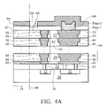
- FIG. 4A illustrates a second embodiment of the present invention, wherein seal ring 42 is formed away from scribe line 38 .
- Trench 66 includes at least a portion horizontally between seal ring 42 and scribe line 38 . Further, the entire trench 66 may be between seal ring 42 and scribe line 38 . In this case, the bottom 68 of trench 66 may extend below the interface 62 , wherein the corresponding position of bottom 68 is illustrated using a dashed line. Alternatively, bottom 68 may be substantially leveled to interface 64 or between interfaces 62 and 64 . If, however, trench 66 includes a portion directly over seal ring 42 , the bottom 68 is preferably higher than interface 62 , so that at least one thin passivation layer Pass- 1 remains over metal line 54 .
- Trench 66 may be located anywhere between scribe line 38 and main seal ring 44 .
- FIG. 4B illustrates an alternative embodiment, wherein trench 66 is between seal rings 42 and 44 .
- bottom 68 of trench 66 may also be below interface 62 , or at other positions as shown in dashed lines.
- the cracks propagated along interface 62 may be stopped.
- FIG. 5 illustrates a third embodiment of the present invention, wherein no sacrificial seal ring is formed.
- Seal ring 44 is spaced apart from scribe line 38 .
- the distance D is at least great enough to accommodate trench 66 .
- distance D is greater than about 2 ⁇ m.
- Trench 66 is formed substantially adjoining, but outside of scribe line 38 , and it is preferable that in the die sawing, the kerf will not cut through trench 66 .
- the bottom 68 of trench 66 is preferably at least level to interface 64 , and more preferably between interfaces 62 and 64 , and even more preferably lower than interface 62 .
- Bottom 68 may even extend lower than metal line 58 , but higher than the top low-k dielectric layer 50 .
- the dashed lines illustrate several possible positions of bottoms 68 .
- cracks propagated in USG 52 or above will be stopped by trench 66 , and seal ring 44 provides an additional protection.
- FIG. 6 illustrates a fourth embodiment of the present invention, wherein aluminum ring AP is formed over seal ring 42 instead of seal ring 44 .
- trench 66 may be formed anywhere between scribe line 38 and the right boundary of seal ring 44 .
- Several exemplary positions of trench 66 and bottom 68 are illustrated with dashed lines. Again, depending on the position of trench 66 , the bottom 68 may be within passivation layers Pass- 2 , Pass- 1 , USG 52 or at their interfaces.
- FIGS. 7 through 9B illustrate single-passivation schemes, in which only one passivation layer is formed. Accordingly, no aluminum pad APs are formed.
- This type of seal ring may be used in direct-bump-on copper applications.
- passivation layer Pass- 1 is formed over USG 52 and metal lines 54 and 58 .
- Trench 66 is preferably formed between seal ring 42 and scribe line 38 . Accordingly, cracks are blocked before they reach seal ring 42 .
- trench 66 may be formed anywhere between scribe line 38 and the right edge (inner edge) of seal ring 44 .
- the bottom 68 of trench 66 may be at different positions, as illustrated by dashed lines.
- via 56 comprises at least two, and may be more, thin via bars 70 instead of a single wide via bar.
- Thin via bars 70 may be separated by the same dielectric material for forming dielectric layer 52 , preferably USG.
- Each of the via bars 70 also forms a ring.
- the width W 4 of via bars 70 is preferably less than about 0.4 ⁇ m. Also, width W 4 is preferably less than about 20 percent of the width W 2 of metal line 54 . It is realized that after the die saw, and in subsequent under-bump metallurgy (UBM) etching process, if the acid is in contact with metal line 54 , metal line 54 may be etched.
- UBM under-bump metallurgy
- trench 66 may be formed directly over seal ring 42 with a part or an entirety of metal line 54 exposed through trench 66 .
- the bottom 68 of trench 66 is lower than the top surface of metal line 54 , with a difference D of greater than about 200 ⁇ .
- the overlap of trench 66 and metal line 54 blocks the crack path along interface 62 , and any other paths above interface 62 .
- trench 66 is located with at least one portion between seal ring 42 and scribe line 38 . Alternatively, the entire trench 66 may be between scribe line 38 and seal ring 42 . Again, the bottom 68 of trench 66 is preferably leveled to interface 62 , and more preferably below interface 62 , with difference D′ of greater than about 200 ⁇ . FIG. 8B also illustrates other possible locations of trenches 66 and bottoms 68 .
- FIG. 9A illustrates yet another embodiment having the single-passivation scheme.
- USG 52 is formed after the formation of metal lines 46 and vias 48 in dielectric layers 50 .
- Metal lines 54 and 58 and vias 56 and 60 are then formed by forming openings in USG 52 , filling the openings, and performing a chemical mechanical polish to remove excess filling materials, leaving metal lines 54 and 58 and vias 56 and 60 .
- a dry etching or wet etching is then performed to recess the top surface 62 of USG 52 .
- the recessing distance D′ is preferably greater than about 200 ⁇ .
- a crack is propagated along interface 62 , it will encounter the protruding portion of metal line 54 , and will be stopped.
- trench 66 is further formed between scribe line 38 and seal ring 42 .
- the bottom 68 of trench 66 is preferably at least lower then the top surface of metal line 54 , and more preferably level with interface 62 .
- the bottom 68 may also be anywhere lower than interface 62 but higher than the bottom surface of USG 52 .
- via 56 includes at least two thin via bars 70 , which are essentially the same as in FIGS. 8A and 8B . Therefore, even if the crack caused by the die saw results in the exposure of metal line 54 through trench 66 , thin via bars 70 will protect seal ring 42 from being etched in the subsequent UBM etching.
- the interfaces 62 may be recessed using essentially the same method as shown in FIGS. 9A and 9B . Accordingly, trenches 66 and the recessing of the interfaces 62 are combined so that cracks are even less likely to penetrate into integrated circuits.
- trench 66 may be filled with either a underfill or a molding compound, depending on the packing process.
- seal rings 42 and 44 each includes metal lines 46 and 54 / 58 , and continuous via bars 48 and 56 / 60 .
- the continuous via bars 48 and 56 / 60 preferably have widths greater than about 70% of the widths of the overlying metal lines 46 and 54 / 58 , and may even be close to, or substantially equal to, the widths of respective metal lines 46 and 54 / 58 .
- the smaller width of the via openings cause etching difficulty, particularly for 90 nm technology and below.
- FIGS. 10A through 12 may be combined with the embodiments discussed in preceding paragraphs in order to achieve stronger seal ring structures and a better crack-prevention ability without causing significant process difficulty.
- metal lines 46 , 54 , and 58 in FIGS. 10A through 12 may have tilted edges, similar to the embodiment shown in FIG. 3A .
- seal rings 42 and 44 each includes portions in top dielectric layers 52 and portions in low-k dielectric layers 50 .
- top dielectric layers 52 are preferably formed of USG, although they can be formed of other materials that are denser, and mechanically stronger, than the low-k dielectric materials in low-k dielectric layers 50 .
- vias 60 are preferably continuous via bars having width W 6 greater than about 70 percent of the width W 5 of the respective overlying metal lines 58 . Width W 6 may even be substantially equal to the width W 5 of the respective overlying metal lines 58 .
- FIG. 10B illustrates a top view of the embodiment shown in FIG. 10A , wherein the cross-sectional view is taken along line A-A′ in FIG. 10A .
- the vias connecting two layers of seal ring 42 includes via bar 80 and vias 82 (referred to as discrete vias hereinafter).
- Via bar 80 forms a ring extending along the perimeter of the respective semiconductor chip.
- Discrete vias 82 form a line parallel to via bar 80 .
- the line formed of discrete vias 82 extends along the four edges of the respective semiconductor chip, and also has a ring-like shape.
- Seal ring 44 includes via bars 84 and discrete vias 86 .
- discrete vias 86 form an array, and the array extends along the edges of the respective semiconductor chip to form a ring-like structure.
- one of the via bars 84 is on an inner side of vias 86 , and the other is on an outer side (the side close to the edge of the respective semiconductor chip) of discrete vias 86 .
- via bars 84 may be formed between discrete vias 86 .
- additional via bars which are similar to via bars 84 , may be inserted between discrete vias 86 .
- Discrete vias 82 and 86 each may have a width W 9 equal to a length L 9 .
- the length L 9 and width W 9 are different, but are comparable, with a ratio of length to width being less than about 2. It is realized that if the width of seal ring 42 is great enough, more discrete vias 82 may be added to form a via array similar to discrete vias 86 .
- the etching difficulty resulting from etching large dielectric areas for via openings is reduced.
- FIGS. 11A and 11B respectfully illustrate a cross-sectional view and a top view of a variation of the embodiment shown in FIGS. 10A and 10B , wherein seal rings 42 and 44 only include via bars in low-k dielectric layers 50 .
- metal lines 58 and continuous via bars 60 which are formed in top dielectric layers 50 , are essentially the same as shown in FIG. 10A .
- via bars 80 and 84 each forming a ring, connect the respective overlying and underlying metal lines 46 .
- Each of the via bars 80 and 84 has a width substantially less than a half of the width of the overlying/underlying metal lines 46 .
- Low-k dielectric materials fill the spaces between via bars 80 and the spaces between via bars 84 .
- there are two via bars 80 each connected to an edge portion of metal lines 46 .
- the optimum number of via bars 80 and 84 depends on the width of the metal lines 46 , and may be determined by experiments to satisfy both the requirement for improving the mechanical strength of seal ring 44 , and the requirement for improving the formation of via openings.
- FIGS. 11A and 11B may be reinforced, as shown in FIG. 12 .
- the cross-sectional view of this embodiment is similar to what is shown in FIG. 11A .
- metal lines 58 and continuous via bars 60 are essentially the same as shown in FIGS. 10A and 10B .
- via bars 80 and 84 are formed to connect the respective overlying and underlying metal lines 46 .
- FIG. 12 is a top view, which shows via buttresses 88 formed between via bars 80 and 84 . Via buttresses 88 are formed simultaneously as, and are seamlessly connected to, via bars 80 and 84 .
- a ratio of width W 7 of via buttresses 88 to width W 8 of via bars 84 is between about 0.8 and about 0.9, and more preferably equal to about one.
- a ratio of distance D 1 between via buttresses 88 to distance D 2 between via bars 80 (and/or via bars 84 ) is preferably between about 4 and about 5.
- FIG. 12 Please note that if a cross-sectional view is taken along a plane crossing line B-B′ in FIG. 12 , the cross-sectional view is similar to what is shown in FIG. 11A . However, if a cross-sectional view is taken along a plane crossing line C-C′ in FIG. 12 , via buttresses 88 and via bars 80 and 84 will appear like a continuous via bar as shown in FIGS. 3A and 3B .
- a semiconductor chip may have only one dielectric layer 52 . Accordingly, it is preferable that only the dielectric layer 52 includes continuous via bars, while the underlying low-k dielectric layers all include thinner via bars, which may be combined with discrete vias or via buttresses. In other embodiments, the schemes having discrete vias or via buttresses, and continuous via bars may be used in any of the top electric layers 52 and low-k dielectric layers 50 , in any combination.
- the embodiments of the present invention have improved ability for preventing cracks from propagating into circuit regions.
- the enhanced protection schemes provide two-fold protection, one with a trench and one with a solid seal ring. Accordingly, the likelihood of the cracks propagating into circuit regions is significantly reduced.
Abstract
Description
Claims (13)
Priority Applications (2)
| Application Number | Priority Date | Filing Date | Title |
|---|---|---|---|
| US11/933,931 US8643147B2 (en) | 2007-11-01 | 2007-11-01 | Seal ring structure with improved cracking protection and reduced problems |
| CN2008100863015A CN101425483B (en) | 2007-11-01 | 2008-03-25 | Integrated circuit structure |
Applications Claiming Priority (1)
| Application Number | Priority Date | Filing Date | Title |
|---|---|---|---|
| US11/933,931 US8643147B2 (en) | 2007-11-01 | 2007-11-01 | Seal ring structure with improved cracking protection and reduced problems |
Publications (2)
| Publication Number | Publication Date |
|---|---|
| US20090115024A1 US20090115024A1 (en) | 2009-05-07 |
| US8643147B2 true US8643147B2 (en) | 2014-02-04 |
Family
ID=40587260
Family Applications (1)
| Application Number | Title | Priority Date | Filing Date |
|---|---|---|---|
| US11/933,931 Active 2029-05-15 US8643147B2 (en) | 2007-11-01 | 2007-11-01 | Seal ring structure with improved cracking protection and reduced problems |
Country Status (2)
| Country | Link |
|---|---|
| US (1) | US8643147B2 (en) |
| CN (1) | CN101425483B (en) |
Cited By (3)
| Publication number | Priority date | Publication date | Assignee | Title |
|---|---|---|---|---|
| US20150137388A1 (en) * | 2013-11-21 | 2015-05-21 | Eun-ji Kim | Semiconductor devices |
| US11004805B2 (en) * | 2019-08-16 | 2021-05-11 | Winbond Electronics Corp. | Semiconductor device and method of fabricating same including two seal rings |
| US11251144B2 (en) * | 2016-11-14 | 2022-02-15 | Samsung Electronics Co., Ltd. | Semiconductor chip |
Families Citing this family (28)
| Publication number | Priority date | Publication date | Assignee | Title |
|---|---|---|---|---|
| US8624346B2 (en) | 2005-10-11 | 2014-01-07 | Taiwan Semiconductor Manufacturing Company, Ltd. | Exclusion zone for stress-sensitive circuit design |
| KR100995558B1 (en) * | 2007-03-22 | 2010-11-22 | 후지쯔 세미컨덕터 가부시키가이샤 | Semiconductor device and method of producing semiconductor device |
| US7952167B2 (en) | 2007-04-27 | 2011-05-31 | Taiwan Semiconductor Manufacturing Company, Ltd. | Scribe line layout design |
| US8125052B2 (en) * | 2007-05-14 | 2012-02-28 | Taiwan Semiconductor Manufacturing Co., Ltd. | Seal ring structure with improved cracking protection |
| JP5106933B2 (en) * | 2007-07-04 | 2012-12-26 | ラピスセミコンダクタ株式会社 | Semiconductor device |
| US8643147B2 (en) | 2007-11-01 | 2014-02-04 | Taiwan Semiconductor Manufacturing Company, Ltd. | Seal ring structure with improved cracking protection and reduced problems |
| US8334582B2 (en) * | 2008-06-26 | 2012-12-18 | Taiwan Semiconductor Manufacturing Company, Ltd. | Protective seal ring for preventing die-saw induced stress |
| US7906836B2 (en) | 2008-11-14 | 2011-03-15 | Taiwan Semiconductor Manufacturing Company, Ltd. | Heat spreader structures in scribe lines |
| US8368180B2 (en) * | 2009-02-18 | 2013-02-05 | Taiwan Semiconductor Manufacturing Company, Ltd. | Scribe line metal structure |
| US20110006389A1 (en) * | 2009-07-08 | 2011-01-13 | Lsi Corporation | Suppressing fractures in diced integrated circuits |
| US8124448B2 (en) * | 2009-09-18 | 2012-02-28 | Advanced Micro Devices, Inc. | Semiconductor chip with crack deflection structure |
| US8436472B2 (en) * | 2010-02-09 | 2013-05-07 | Taiwan Semiconductor Manufacturing Company, Ltd. | Corner stress release structure design for increasing circuit routing areas |
| DE102010029528A1 (en) * | 2010-05-31 | 2011-12-01 | GLOBALFOUNDRIES Dresden Module One Ltd. Liability Company & Co. KG | Semiconductor device having a chip border with a gradual density of structure |
| ITMI20101415A1 (en) * | 2010-07-29 | 2012-01-30 | St Microelectronics Srl | TRACEABLE INTEGRATED CIRCUITS AND RELATED PRODUCTION METHOD |
| US8710630B2 (en) * | 2011-07-11 | 2014-04-29 | Taiwan Semiconductor Manufacturing Company, Ltd. | Mechanisms for marking the orientation of a sawed die |
| US8587090B2 (en) | 2011-07-29 | 2013-11-19 | Mediatek Inc. | Die seal ring structure |
| US9478505B2 (en) | 2012-04-12 | 2016-10-25 | Taiwan Semiconductor Manufacturing Co., Ltd. | Guard ring design structure for semiconductor devices |
| CN107359139B (en) * | 2012-07-19 | 2019-11-12 | 瑞萨电子株式会社 | Semiconductor device |
| JP5968711B2 (en) * | 2012-07-25 | 2016-08-10 | ルネサスエレクトロニクス株式会社 | Semiconductor device and manufacturing method of semiconductor device |
| JP6132525B2 (en) * | 2012-11-30 | 2017-05-24 | ルネサスエレクトロニクス株式会社 | Semiconductor device and manufacturing method thereof |
| TWI495074B (en) | 2012-11-30 | 2015-08-01 | Ind Tech Res Inst | Stress relief structure |
| US20170256506A1 (en) * | 2013-01-11 | 2017-09-07 | Renesas Electronics Corporation | Semiconductor device |
| CN105845665B (en) * | 2015-01-16 | 2018-10-23 | 中芯国际集成电路制造(上海)有限公司 | A kind of semiconductor devices and preparation method thereof and electronic device |
| US9589903B2 (en) | 2015-03-16 | 2017-03-07 | Taiwan Semiconductor Manufacturing Company, Ltd. | Eliminate sawing-induced peeling through forming trenches |
| CN106356383B (en) * | 2015-07-17 | 2020-02-07 | 中芯国际集成电路制造(上海)有限公司 | Semiconductor structure, semiconductor device, chip structure and forming method thereof |
| CN107316817B (en) * | 2016-04-26 | 2020-08-25 | 中芯国际集成电路制造(上海)有限公司 | Package and method of manufacturing the same |
| US11640934B2 (en) * | 2018-03-30 | 2023-05-02 | Intel Corporation | Lithographically defined vertical interconnect access (VIA) in dielectric pockets in a package substrate |
| US11348881B2 (en) * | 2019-10-01 | 2022-05-31 | Taiwan Semiconductor Manufacturing Company, Ltd. | Device crack-stop structure to prevent damage due to dicing crack |
Citations (101)
| Publication number | Priority date | Publication date | Assignee | Title |
|---|---|---|---|---|
| US4364078A (en) | 1978-08-15 | 1982-12-14 | Synertek | Edge barrier of polysilicon and metal for integrated circuit chips |
| US4835592A (en) | 1986-03-05 | 1989-05-30 | Ixys Corporation | Semiconductor wafer with dice having briding metal structure and method of manufacturing same |
| US5047711A (en) | 1989-08-23 | 1991-09-10 | Silicon Connections Corporation | Wafer-level burn-in testing of integrated circuits |
| US5096855A (en) | 1988-05-23 | 1992-03-17 | U.S. Philips Corporation | Method of dicing semiconductor wafers which produces shards less than 10 microns in size |
| US5136364A (en) | 1991-06-12 | 1992-08-04 | National Semiconductor Corporation | Semiconductor die sealing |
| US5206181A (en) | 1991-06-03 | 1993-04-27 | Motorola, Inc. | Method for manufacturing a semiconductor device with a slotted metal test pad to prevent lift-off during wafer scribing |
| US5239191A (en) | 1990-01-19 | 1993-08-24 | Kabushiki Kaisha Toshiba | Semiconductor wafer |
| US5285082A (en) | 1989-11-08 | 1994-02-08 | U.S. Philips Corporation | Integrated test circuits having pads provided along scribe lines |
| US5371411A (en) | 1980-09-01 | 1994-12-06 | Hitachi, Ltd. | Resin molded type semiconductor device having a conductor film |
| US5391920A (en) | 1991-07-09 | 1995-02-21 | Yamaha Corporation | Semiconductor device having peripheral metal wiring |
| US5559362A (en) | 1993-10-27 | 1996-09-24 | Nec Corporation | Semiconductor device having double metal connection layers connected to each other and to the substrate in the scribe line area |
| US5751065A (en) | 1993-08-05 | 1998-05-12 | Lucent Technologies Inc. | Integrated circuit with active devices under bond pads |
| US5831330A (en) | 1996-06-28 | 1998-11-03 | Winbond Electronics Corp. | Die seal structure for a semiconductor integrated circuit |
| US5834829A (en) | 1996-09-05 | 1998-11-10 | International Business Machines Corporation | Energy relieving crack stop |
| US5892284A (en) | 1997-04-21 | 1999-04-06 | Nec Corporation | Semiconductor integrated circuit |
| US6022791A (en) | 1997-10-15 | 2000-02-08 | International Business Machines Corporation | Chip crack stop |
| US6114766A (en) | 1997-12-18 | 2000-09-05 | Advanced Micro Devices, Inc. | Integrated circuit with metal features presenting a larger landing area for vias |
| US6121677A (en) | 1997-12-31 | 2000-09-19 | Samsung Electronics Co. | Reduced size integrated circuits and methods using test pads located in scribe regions of integrated circuits wafers |
| US20010005617A1 (en) | 1999-12-21 | 2001-06-28 | Robert Feurle | Dicing configuration for separating a semiconductor component from a semiconductor wafer |
| US20010005604A1 (en) | 1999-12-22 | 2001-06-28 | Samsung Electronics Co., Ltd. | Fuse area structure including protection film on sidewall of fuse opening in semiconductor device and method of forming the same |
| US20010008296A1 (en) | 1999-07-15 | 2001-07-19 | Tito Gelsomini | Integrated circuit wireless tagging |
| US6284657B1 (en) | 2000-02-25 | 2001-09-04 | Chartered Semiconductor Manufacturing Ltd. | Non-metallic barrier formation for copper damascene type interconnects |
| US20010019848A1 (en) | 1999-05-07 | 2001-09-06 | Misewich James A. | Process for fabrication of an all-epitaxial-oxide transistor |
| US6300223B1 (en) | 1996-12-12 | 2001-10-09 | Winbond Electronics Corp. | Method of forming die seal structures having substrate trenches |
| US20020024115A1 (en) | 1998-02-06 | 2002-02-28 | Ibnabdeljalil M?Apos;Hamed | Sacrificial structures for arresting insulator cracks in semiconductor devices |
| US6358839B1 (en) | 2000-05-26 | 2002-03-19 | Taiwan Semiconductor Manufacturing Company | Solution to black diamond film delamination problem |
| US6372409B1 (en) | 1999-05-07 | 2002-04-16 | Taiwan Semiconductor Manufacturing Company, Ltd | Bonds pads equipped with heat dissipating rings and method for forming |
| US6384463B1 (en) | 1998-09-03 | 2002-05-07 | Telefonaktiebolaget Lm Ericsson (Publ) | High voltage shield |
| US20020130394A1 (en) | 2001-01-17 | 2002-09-19 | Yoshihiko Toyoda | Semiconductor device and manufacturing method thereof |
| US6492716B1 (en) | 2001-04-30 | 2002-12-10 | Zeevo, Inc. | Seal ring structure for IC containing integrated digital/RF/analog circuits and functions |
| US6495918B1 (en) | 2000-09-05 | 2002-12-17 | Infineon Technologies Ag | Chip crack stop design for semiconductor chips |
| US20030003677A1 (en) | 2001-06-27 | 2003-01-02 | Canon Kabushiki Kaisha | Alignment method, exposure apparatus and device fabrication method |
| US6521975B1 (en) | 1999-05-20 | 2003-02-18 | Texas Instruments Incorporated | Scribe street seals in semiconductor devices and method of fabrication |
| US6566736B1 (en) | 2001-11-30 | 2003-05-20 | Advanced Micro Devices, Inc. | Die seal for semiconductor device moisture protection |
| US20040084777A1 (en) | 2002-10-30 | 2004-05-06 | Fujitsu Limited | Semiconductor device and method for fabricating the same |
| US20040119164A1 (en) | 2002-08-15 | 2004-06-24 | Nobuyuki Kurashima | Semiconductor device and its manufacturing method |
| US20040150070A1 (en) | 2003-02-03 | 2004-08-05 | Nec Electronics Corporation | Semiconductor device and method for manufacturing the same |
| US20040150073A1 (en) | 2003-01-30 | 2004-08-05 | Nec Electronics Corporation | Semiconductor device having superior resistance to moisture |
| US6796024B2 (en) | 1999-12-13 | 2004-09-28 | Fujitsu Limited | Method for making semiconductor device |
| US6806168B2 (en) | 2002-11-27 | 2004-10-19 | Intel Corporation | Healing of micro-cracks in an on-chip dielectric |
| CN1542505A (en) | 2003-11-05 | 2004-11-03 | 友达光电股份有限公司 | Display assembly and assembling method thereof |
| US20050009300A1 (en) | 2000-06-06 | 2005-01-13 | Stmicroelectronics S.R.L. | Electronic semiconductor device having a thermal spreader |
| US20050017363A1 (en) | 2003-07-25 | 2005-01-27 | Kang-Cheng Lin | Semiconductor device with anchor type seal ring |
| US20050026397A1 (en) | 2003-07-28 | 2005-02-03 | International Business Machines Corporation | Crack stop for low k dielectrics |
| US6861755B2 (en) | 2002-10-30 | 2005-03-01 | Fujitsu Limited | Semiconductor device |
| US20050046015A1 (en) | 2003-08-28 | 2005-03-03 | St Assembly Test Services Ltd. | Array-molded package heat spreader and fabrication method therefor |
| US6876946B2 (en) | 1993-01-21 | 2005-04-05 | Nikon Corporation | Alignment method and apparatus therefor |
| US6876062B2 (en) | 2002-06-27 | 2005-04-05 | Taiwan Semiconductor Manufacturing Co., Ltd | Seal ring and die corner stress relief pattern design to protect against moisture and metallic impurities |
| US20050098893A1 (en) * | 2003-11-10 | 2005-05-12 | Matsushita Electric Industrial Co., Ltd. | Semiconductor device and method for fabricating the same |
| US20050148115A1 (en) | 2000-02-10 | 2005-07-07 | Williams Vernon M. | Programmed material consolidation methods for fabricating heat sinks |
| US20050151239A1 (en) * | 2004-01-14 | 2005-07-14 | Taiwan Semiconductor Manufacturing Co., Ltd. | Integrated circuit devices, edge seals therefor |
| US6939736B2 (en) | 2003-07-31 | 2005-09-06 | Texas Instruments Incorporated | Ideal operational amplifier layout techniques for reducing package stress and configurations therefor |
| US20050230005A1 (en) | 2003-06-25 | 2005-10-20 | Taiwan Semiconductor Manufacturing Co., Ltd. | Test pad for reducing die sawing damage |
| US20050236672A1 (en) | 2004-04-22 | 2005-10-27 | Nec Electronics Corporation | MOS type semiconductor device having electrostatic discharge protection arrangement |
| CN1701418A (en) | 2003-04-30 | 2005-11-23 | 富士通株式会社 | Semiconductor device producing method, semiconductor wafer and semiconductor device |
| US20050280120A1 (en) | 2004-06-21 | 2005-12-22 | Renesas Technology Corp. | Semiconductor device |
| US20060001144A1 (en) | 2004-06-30 | 2006-01-05 | Uehling Trent S | Scribe street structure for backend interconnect semiconductor wafer integration |
| US20060012012A1 (en) | 2004-07-15 | 2006-01-19 | Ping-Wei Wang | Semiconductor device with crack prevention ring and method of manufacture thereof |
| US20060022195A1 (en) | 2004-08-01 | 2006-02-02 | Kun-Chih Wang | Scribe line structure |
| US20060055002A1 (en) | 2004-09-13 | 2006-03-16 | Taiwan Semiconductor Manufacturing Co. | Methods for enhancing die saw and packaging reliability |
| US20060088984A1 (en) | 2004-10-21 | 2006-04-27 | Intel Corporation | Laser ablation method |
| US20060103025A1 (en) | 2004-11-15 | 2006-05-18 | Renesas Technology Corp. | Semiconductor device including sealing ring |
| US20060125090A1 (en) | 2004-04-22 | 2006-06-15 | Taiwan Semiconductor Manufacturing Co., Ltd. | Heat dissipation structure and method thereof |
| US20060172457A1 (en) | 2005-02-02 | 2006-08-03 | Siliconware Precision Industries Co., Ltd. | Chip-stacked semiconductor package and method for fabricating the same |
| US7087452B2 (en) | 2003-04-22 | 2006-08-08 | Intel Corporation | Edge arrangements for integrated circuit chips |
| US20060192265A1 (en) * | 2005-02-25 | 2006-08-31 | Yu-Hao Hsu | System-on-chip with shield rings for shielding functional blocks therein from electromagnetic interference |
| US7126255B2 (en) | 2004-04-05 | 2006-10-24 | Ngk Insulators, Ltd. | Piezoelectric/electrostrictive film-type device |
| US7126225B2 (en) | 2003-04-15 | 2006-10-24 | Taiwan Semiconductor Manufacturing Company, Ltd. | Apparatus and method for manufacturing a semiconductor wafer with reduced delamination and peeling |
| US7129565B2 (en) | 2002-03-15 | 2006-10-31 | Fujitsu Limited | Semiconductor device, method of manufacturing the same, and phase shift mask |
| US7135384B2 (en) | 2003-02-28 | 2006-11-14 | Kabushiki Kaisha Toshiba | Semiconductor wafer dividing method and apparatus |
| US7138700B2 (en) | 2003-04-01 | 2006-11-21 | Nec Electronics Corporation | Semiconductor device with guard ring for preventing water from entering circuit region from outside |
| US7138297B2 (en) | 2003-01-14 | 2006-11-21 | Kabushiki Kaisha Toshiba | Method of dividing a semiconductor wafer utilizing a laser dicing technique |
| US7145211B2 (en) | 2004-07-13 | 2006-12-05 | Micrel, Incorporated | Seal ring for mixed circuitry semiconductor devices |
| US20070018331A1 (en) | 2005-07-25 | 2007-01-25 | Taiwan Semiconductor Manufacturing Company, Ltd. | Dummy structures extending from seal ring into active circuit area of integrated circuit chip |
| US20070018279A1 (en) | 2005-07-21 | 2007-01-25 | Taiwan Semiconductor Manufacturing Co. | Protection layer for preventing laser damage on semiconductor devices |
| US20070031996A1 (en) | 2003-04-26 | 2007-02-08 | Chopin Sheila F | Packaged integrated circuit having a heat spreader and method therefor |
| US20070090547A1 (en) | 2005-10-11 | 2007-04-26 | Taiwan Semiconductor Manufacturing Company, Ltd. | Exclusion zone for stress-sensitive circuit design |
| US20070090447A1 (en) | 2005-10-25 | 2007-04-26 | Renesas Technology Corp. | Semiconductor device and method of manufacture thereof |
| US7235834B2 (en) | 2004-09-02 | 2007-06-26 | Seiko Epson Corporation | Ferroelectric memory and its manufacturing method |
| US20070158788A1 (en) * | 2006-01-12 | 2007-07-12 | Taiwan Semiconductor Manufacturing Co., Ltd. | Die seal structure for reducing stress induced during die saw process |
| US7259445B2 (en) | 2002-09-30 | 2007-08-21 | Advanced Interconnect Technologies Limited | Thermal enhanced package for block mold assembly |
| US7291874B2 (en) | 2004-12-14 | 2007-11-06 | Arima Optoelectronics Corp. | Laser dicing apparatus for a gallium arsenide wafer and method thereof |
| US20070262435A1 (en) | 2006-04-27 | 2007-11-15 | Atmel Corporation | Three-dimensional packaging scheme for package types utilizing a sacrificial metal base |
| US20080054263A1 (en) | 2006-09-04 | 2008-03-06 | Samsung Electronics Co., Ltd. | Semiconductor device and method of fabricating the same |
| US20080067672A1 (en) | 2006-09-14 | 2008-03-20 | Fujitsu Limited | Semiconductor device and method for fabricating the same |
| US7387950B1 (en) | 2006-12-17 | 2008-06-17 | United Microelectronics Corp. | Method for forming a metal structure |
| US20080157284A1 (en) | 2006-12-29 | 2008-07-03 | Nicole Meier Chang | Guard ring extension to prevent reliability failures |
| US7407835B2 (en) | 2001-12-14 | 2008-08-05 | Taiwan Semiconductor Manufacturing Company | Localized slots for stress relieve in copper |
| US20080213938A1 (en) | 2007-03-01 | 2008-09-04 | Ching-Hung Kao | Method for fabricating a cmos image sensor |
| US20080265378A1 (en) | 2007-04-27 | 2008-10-30 | Hsin-Hui Lee | Scribe line layout design |
| US20080283969A1 (en) | 2007-05-14 | 2008-11-20 | Jeng Shin-Puu | Seal Ring Structure with Improved Cracking Protection |
| US20080299708A1 (en) | 2004-09-24 | 2008-12-04 | Matsushita Electric Industrial Co., Ltd. | Electronic device and method for fabricating the same |
| US20090115025A1 (en) | 2007-11-07 | 2009-05-07 | Oh-Jin Jung | Semiconductor device and method for manufacturing the same |
| US20090115024A1 (en) | 2007-11-01 | 2009-05-07 | Jeng Shin-Puu | Seal ring structure with improved cracking protection and reduced problems |
| US20090302445A1 (en) | 2008-06-09 | 2009-12-10 | Stats Chippac, Ltd. | Method and Apparatus for Thermally Enhanced Semiconductor Package |
| US20090315184A1 (en) | 2008-05-26 | 2009-12-24 | Oki Semiconductor Co., Ltd. | Semiconductor Device |
| US20090321890A1 (en) | 2008-06-26 | 2009-12-31 | Jeng Shin-Puu | Protective Seal Ring for Preventing Die-Saw Induced Stress |
| US7646078B2 (en) | 2007-01-17 | 2010-01-12 | Taiwan Semiconductor Manufacturing Company, Ltd. | Die saw crack stopper |
| US20100123219A1 (en) | 2008-11-14 | 2010-05-20 | Hsien-Wei Chen | Heat Spreader Structures in Scribe Lines |
| US20100207251A1 (en) | 2009-02-18 | 2010-08-19 | Chen-Hua Yu | Scribe Line Metal Structure |
| US7888794B2 (en) | 2008-02-18 | 2011-02-15 | Infineon Technologies Ag | Semiconductor device and method |
Family Cites Families (6)
| Publication number | Priority date | Publication date | Assignee | Title |
|---|---|---|---|---|
| US96855A (en) * | 1869-11-16 | Geoegb wellhouse | ||
| US6393825B1 (en) * | 2000-01-25 | 2002-05-28 | General Electric Company | System for pressure modulation of turbine sidewall cavities |
| US20040119184A1 (en) * | 2002-12-23 | 2004-06-24 | Lear Corporation | Method for foaming in place headliner structures |
| US6841466B1 (en) * | 2003-09-26 | 2005-01-11 | Taiwan Semiconductor Manufacturing Company | Method of selectively making copper using plating technology |
| US7219832B2 (en) * | 2004-06-17 | 2007-05-22 | First Data Corporation | ATM machine and methods with currency conversion capabilities |
| CN100481455C (en) * | 2005-12-22 | 2009-04-22 | 中芯国际集成电路制造(上海)有限公司 | Seal ring structure with incomplete contact through hole stack |
-
2007
- 2007-11-01 US US11/933,931 patent/US8643147B2/en active Active
-
2008
- 2008-03-25 CN CN2008100863015A patent/CN101425483B/en active Active
Patent Citations (126)
| Publication number | Priority date | Publication date | Assignee | Title |
|---|---|---|---|---|
| US4364078A (en) | 1978-08-15 | 1982-12-14 | Synertek | Edge barrier of polysilicon and metal for integrated circuit chips |
| US5371411A (en) | 1980-09-01 | 1994-12-06 | Hitachi, Ltd. | Resin molded type semiconductor device having a conductor film |
| US4835592A (en) | 1986-03-05 | 1989-05-30 | Ixys Corporation | Semiconductor wafer with dice having briding metal structure and method of manufacturing same |
| US5096855A (en) | 1988-05-23 | 1992-03-17 | U.S. Philips Corporation | Method of dicing semiconductor wafers which produces shards less than 10 microns in size |
| US5047711A (en) | 1989-08-23 | 1991-09-10 | Silicon Connections Corporation | Wafer-level burn-in testing of integrated circuits |
| US5285082A (en) | 1989-11-08 | 1994-02-08 | U.S. Philips Corporation | Integrated test circuits having pads provided along scribe lines |
| US5239191A (en) | 1990-01-19 | 1993-08-24 | Kabushiki Kaisha Toshiba | Semiconductor wafer |
| US5206181A (en) | 1991-06-03 | 1993-04-27 | Motorola, Inc. | Method for manufacturing a semiconductor device with a slotted metal test pad to prevent lift-off during wafer scribing |
| US5136364A (en) | 1991-06-12 | 1992-08-04 | National Semiconductor Corporation | Semiconductor die sealing |
| US5391920A (en) | 1991-07-09 | 1995-02-21 | Yamaha Corporation | Semiconductor device having peripheral metal wiring |
| US6876946B2 (en) | 1993-01-21 | 2005-04-05 | Nikon Corporation | Alignment method and apparatus therefor |
| US5751065A (en) | 1993-08-05 | 1998-05-12 | Lucent Technologies Inc. | Integrated circuit with active devices under bond pads |
| US5559362A (en) | 1993-10-27 | 1996-09-24 | Nec Corporation | Semiconductor device having double metal connection layers connected to each other and to the substrate in the scribe line area |
| US5831330A (en) | 1996-06-28 | 1998-11-03 | Winbond Electronics Corp. | Die seal structure for a semiconductor integrated circuit |
| US5834829A (en) | 1996-09-05 | 1998-11-10 | International Business Machines Corporation | Energy relieving crack stop |
| US6300223B1 (en) | 1996-12-12 | 2001-10-09 | Winbond Electronics Corp. | Method of forming die seal structures having substrate trenches |
| US5892284A (en) | 1997-04-21 | 1999-04-06 | Nec Corporation | Semiconductor integrated circuit |
| US6022791A (en) | 1997-10-15 | 2000-02-08 | International Business Machines Corporation | Chip crack stop |
| US6114766A (en) | 1997-12-18 | 2000-09-05 | Advanced Micro Devices, Inc. | Integrated circuit with metal features presenting a larger landing area for vias |
| US6121677A (en) | 1997-12-31 | 2000-09-19 | Samsung Electronics Co. | Reduced size integrated circuits and methods using test pads located in scribe regions of integrated circuits wafers |
| US6365958B1 (en) | 1998-02-06 | 2002-04-02 | Texas Instruments Incorporated | Sacrificial structures for arresting insulator cracks in semiconductor devices |
| US20020024115A1 (en) | 1998-02-06 | 2002-02-28 | Ibnabdeljalil M?Apos;Hamed | Sacrificial structures for arresting insulator cracks in semiconductor devices |
| US6384463B1 (en) | 1998-09-03 | 2002-05-07 | Telefonaktiebolaget Lm Ericsson (Publ) | High voltage shield |
| US6350622B2 (en) | 1999-05-07 | 2002-02-26 | International Business Machines Corporation | Process for fabrication of an all-epitaxial-oxide transistor |
| US20010019848A1 (en) | 1999-05-07 | 2001-09-06 | Misewich James A. | Process for fabrication of an all-epitaxial-oxide transistor |
| US6372409B1 (en) | 1999-05-07 | 2002-04-16 | Taiwan Semiconductor Manufacturing Company, Ltd | Bonds pads equipped with heat dissipating rings and method for forming |
| US6841455B2 (en) | 1999-05-20 | 2005-01-11 | Texas Instruments Incorporated | Scribe street seals in semiconductor devices and method of fabrication |
| US6521975B1 (en) | 1999-05-20 | 2003-02-18 | Texas Instruments Incorporated | Scribe street seals in semiconductor devices and method of fabrication |
| US20010008296A1 (en) | 1999-07-15 | 2001-07-19 | Tito Gelsomini | Integrated circuit wireless tagging |
| US6796024B2 (en) | 1999-12-13 | 2004-09-28 | Fujitsu Limited | Method for making semiconductor device |
| US20010005617A1 (en) | 1999-12-21 | 2001-06-28 | Robert Feurle | Dicing configuration for separating a semiconductor component from a semiconductor wafer |
| US20010005604A1 (en) | 1999-12-22 | 2001-06-28 | Samsung Electronics Co., Ltd. | Fuse area structure including protection film on sidewall of fuse opening in semiconductor device and method of forming the same |
| US20050148115A1 (en) | 2000-02-10 | 2005-07-07 | Williams Vernon M. | Programmed material consolidation methods for fabricating heat sinks |
| US6284657B1 (en) | 2000-02-25 | 2001-09-04 | Chartered Semiconductor Manufacturing Ltd. | Non-metallic barrier formation for copper damascene type interconnects |
| US6483173B2 (en) | 2000-05-26 | 2002-11-19 | Taiwan Semiconductor Manufacturing Company | Solution to black diamond film delamination problem |
| US6358839B1 (en) | 2000-05-26 | 2002-03-19 | Taiwan Semiconductor Manufacturing Company | Solution to black diamond film delamination problem |
| US20050009300A1 (en) | 2000-06-06 | 2005-01-13 | Stmicroelectronics S.R.L. | Electronic semiconductor device having a thermal spreader |
| US6495918B1 (en) | 2000-09-05 | 2002-12-17 | Infineon Technologies Ag | Chip crack stop design for semiconductor chips |
| US20020130394A1 (en) | 2001-01-17 | 2002-09-19 | Yoshihiko Toyoda | Semiconductor device and manufacturing method thereof |
| US6605861B2 (en) | 2001-01-17 | 2003-08-12 | Mitsubishi Denki Kabushiki Kaisha | Semiconductor device |
| US6492716B1 (en) | 2001-04-30 | 2002-12-10 | Zeevo, Inc. | Seal ring structure for IC containing integrated digital/RF/analog circuits and functions |
| US6963389B2 (en) | 2001-06-27 | 2005-11-08 | Canon Kabushiki Kaisha | Alignment method, exposure apparatus and device fabrication method |
| US20030003677A1 (en) | 2001-06-27 | 2003-01-02 | Canon Kabushiki Kaisha | Alignment method, exposure apparatus and device fabrication method |
| US6566736B1 (en) | 2001-11-30 | 2003-05-20 | Advanced Micro Devices, Inc. | Die seal for semiconductor device moisture protection |
| US7407835B2 (en) | 2001-12-14 | 2008-08-05 | Taiwan Semiconductor Manufacturing Company | Localized slots for stress relieve in copper |
| US7129565B2 (en) | 2002-03-15 | 2006-10-31 | Fujitsu Limited | Semiconductor device, method of manufacturing the same, and phase shift mask |
| US6876062B2 (en) | 2002-06-27 | 2005-04-05 | Taiwan Semiconductor Manufacturing Co., Ltd | Seal ring and die corner stress relief pattern design to protect against moisture and metallic impurities |
| US7042099B2 (en) | 2002-08-15 | 2006-05-09 | Kabushiki Kaisha Toshiba | Semiconductor device containing a dummy wire |
| US20040119164A1 (en) | 2002-08-15 | 2004-06-24 | Nobuyuki Kurashima | Semiconductor device and its manufacturing method |
| US7259445B2 (en) | 2002-09-30 | 2007-08-21 | Advanced Interconnect Technologies Limited | Thermal enhanced package for block mold assembly |
| US6861755B2 (en) | 2002-10-30 | 2005-03-01 | Fujitsu Limited | Semiconductor device |
| US20040084777A1 (en) | 2002-10-30 | 2004-05-06 | Fujitsu Limited | Semiconductor device and method for fabricating the same |
| US6806168B2 (en) | 2002-11-27 | 2004-10-19 | Intel Corporation | Healing of micro-cracks in an on-chip dielectric |
| US7138297B2 (en) | 2003-01-14 | 2006-11-21 | Kabushiki Kaisha Toshiba | Method of dividing a semiconductor wafer utilizing a laser dicing technique |
| US6876064B2 (en) | 2003-01-30 | 2005-04-05 | Nec Electronics Corporation | Semiconductor device having superior resistance to moisture |
| US20040150073A1 (en) | 2003-01-30 | 2004-08-05 | Nec Electronics Corporation | Semiconductor device having superior resistance to moisture |
| US20040150070A1 (en) | 2003-02-03 | 2004-08-05 | Nec Electronics Corporation | Semiconductor device and method for manufacturing the same |
| US6998712B2 (en) * | 2003-02-03 | 2006-02-14 | Nec Electronics Corporation | Semiconductor device and method for manufacturing the same |
| US7135384B2 (en) | 2003-02-28 | 2006-11-14 | Kabushiki Kaisha Toshiba | Semiconductor wafer dividing method and apparatus |
| US7138700B2 (en) | 2003-04-01 | 2006-11-21 | Nec Electronics Corporation | Semiconductor device with guard ring for preventing water from entering circuit region from outside |
| US7126225B2 (en) | 2003-04-15 | 2006-10-24 | Taiwan Semiconductor Manufacturing Company, Ltd. | Apparatus and method for manufacturing a semiconductor wafer with reduced delamination and peeling |
| US7294937B2 (en) | 2003-04-15 | 2007-11-13 | Taiwan Semiconductor Manufacturing Company, Ltd. | Apparatus and method for manufacturing a semiconductor wafer with reduced delamination and peeling |
| US7087452B2 (en) | 2003-04-22 | 2006-08-08 | Intel Corporation | Edge arrangements for integrated circuit chips |
| US20070031996A1 (en) | 2003-04-26 | 2007-02-08 | Chopin Sheila F | Packaged integrated circuit having a heat spreader and method therefor |
| CN1701418A (en) | 2003-04-30 | 2005-11-23 | 富士通株式会社 | Semiconductor device producing method, semiconductor wafer and semiconductor device |
| US20050269702A1 (en) | 2003-04-30 | 2005-12-08 | Fujitsu Limited | Method for fabricating semiconductor device capable of scribing chips with high yield |
| US20050230005A1 (en) | 2003-06-25 | 2005-10-20 | Taiwan Semiconductor Manufacturing Co., Ltd. | Test pad for reducing die sawing damage |
| US6861754B2 (en) | 2003-07-25 | 2005-03-01 | Taiwan Semiconductor Manufacturing Company Ltd. | Semiconductor device with anchor type seal ring |
| US20050017363A1 (en) | 2003-07-25 | 2005-01-27 | Kang-Cheng Lin | Semiconductor device with anchor type seal ring |
| US20050026397A1 (en) | 2003-07-28 | 2005-02-03 | International Business Machines Corporation | Crack stop for low k dielectrics |
| CN1830079A (en) | 2003-07-28 | 2006-09-06 | 国际商业机器公司 | Crack stop for low K dielectrics |
| US7335577B2 (en) | 2003-07-28 | 2008-02-26 | International Business Machines Corporation | Crack stop for low K dielectrics |
| US6939736B2 (en) | 2003-07-31 | 2005-09-06 | Texas Instruments Incorporated | Ideal operational amplifier layout techniques for reducing package stress and configurations therefor |
| US20050046015A1 (en) | 2003-08-28 | 2005-03-03 | St Assembly Test Services Ltd. | Array-molded package heat spreader and fabrication method therefor |
| CN1542505A (en) | 2003-11-05 | 2004-11-03 | 友达光电股份有限公司 | Display assembly and assembling method thereof |
| US7453128B2 (en) | 2003-11-10 | 2008-11-18 | Panasonic Corporation | Semiconductor device and method for fabricating the same |
| US20050098893A1 (en) * | 2003-11-10 | 2005-05-12 | Matsushita Electric Industrial Co., Ltd. | Semiconductor device and method for fabricating the same |
| US20050151239A1 (en) * | 2004-01-14 | 2005-07-14 | Taiwan Semiconductor Manufacturing Co., Ltd. | Integrated circuit devices, edge seals therefor |
| US7235864B2 (en) | 2004-01-14 | 2007-06-26 | Taiwan Semiconductor Manufacturing Co., Ltd. | Integrated circuit devices, edge seals therefor |
| US7126255B2 (en) | 2004-04-05 | 2006-10-24 | Ngk Insulators, Ltd. | Piezoelectric/electrostrictive film-type device |
| US20060125090A1 (en) | 2004-04-22 | 2006-06-15 | Taiwan Semiconductor Manufacturing Co., Ltd. | Heat dissipation structure and method thereof |
| US20050236672A1 (en) | 2004-04-22 | 2005-10-27 | Nec Electronics Corporation | MOS type semiconductor device having electrostatic discharge protection arrangement |
| US7400028B2 (en) | 2004-06-21 | 2008-07-15 | Renesas Technology Corp. | Semiconductor device |
| US20050280120A1 (en) | 2004-06-21 | 2005-12-22 | Renesas Technology Corp. | Semiconductor device |
| US7129566B2 (en) | 2004-06-30 | 2006-10-31 | Freescale Semiconductor, Inc. | Scribe street structure for backend interconnect semiconductor wafer integration |
| US20060001144A1 (en) | 2004-06-30 | 2006-01-05 | Uehling Trent S | Scribe street structure for backend interconnect semiconductor wafer integration |
| US7145211B2 (en) | 2004-07-13 | 2006-12-05 | Micrel, Incorporated | Seal ring for mixed circuitry semiconductor devices |
| US20060012012A1 (en) | 2004-07-15 | 2006-01-19 | Ping-Wei Wang | Semiconductor device with crack prevention ring and method of manufacture thereof |
| US20060022195A1 (en) | 2004-08-01 | 2006-02-02 | Kun-Chih Wang | Scribe line structure |
| US7235834B2 (en) | 2004-09-02 | 2007-06-26 | Seiko Epson Corporation | Ferroelectric memory and its manufacturing method |
| US20060055007A1 (en) | 2004-09-13 | 2006-03-16 | Taiwan Semiconductor Manufacturing Co., Ltd. | Seal ring structure for integrated circuit chips |
| CN1770432A (en) | 2004-09-13 | 2006-05-10 | 台湾积体电路制造股份有限公司 | Seal ring structure for integrated circuit chips |
| US20060055002A1 (en) | 2004-09-13 | 2006-03-16 | Taiwan Semiconductor Manufacturing Co. | Methods for enhancing die saw and packaging reliability |
| US20080299708A1 (en) | 2004-09-24 | 2008-12-04 | Matsushita Electric Industrial Co., Ltd. | Electronic device and method for fabricating the same |
| US20060088984A1 (en) | 2004-10-21 | 2006-04-27 | Intel Corporation | Laser ablation method |
| US20060103025A1 (en) | 2004-11-15 | 2006-05-18 | Renesas Technology Corp. | Semiconductor device including sealing ring |
| US7291874B2 (en) | 2004-12-14 | 2007-11-06 | Arima Optoelectronics Corp. | Laser dicing apparatus for a gallium arsenide wafer and method thereof |
| US20060172457A1 (en) | 2005-02-02 | 2006-08-03 | Siliconware Precision Industries Co., Ltd. | Chip-stacked semiconductor package and method for fabricating the same |
| US20060192265A1 (en) * | 2005-02-25 | 2006-08-31 | Yu-Hao Hsu | System-on-chip with shield rings for shielding functional blocks therein from electromagnetic interference |
| US20070018279A1 (en) | 2005-07-21 | 2007-01-25 | Taiwan Semiconductor Manufacturing Co. | Protection layer for preventing laser damage on semiconductor devices |
| US20070018331A1 (en) | 2005-07-25 | 2007-01-25 | Taiwan Semiconductor Manufacturing Company, Ltd. | Dummy structures extending from seal ring into active circuit area of integrated circuit chip |
| US20070090547A1 (en) | 2005-10-11 | 2007-04-26 | Taiwan Semiconductor Manufacturing Company, Ltd. | Exclusion zone for stress-sensitive circuit design |
| CN1956173A (en) | 2005-10-25 | 2007-05-02 | 株式会社瑞萨科技 | Semiconductor device and method of manufacture thereof |
| US20070090447A1 (en) | 2005-10-25 | 2007-04-26 | Renesas Technology Corp. | Semiconductor device and method of manufacture thereof |
| US20070158788A1 (en) * | 2006-01-12 | 2007-07-12 | Taiwan Semiconductor Manufacturing Co., Ltd. | Die seal structure for reducing stress induced during die saw process |
| US7456507B2 (en) | 2006-01-12 | 2008-11-25 | Taiwan Semiconductor Manufacturing Co., Ltd. | Die seal structure for reducing stress induced during die saw process |
| US20070262435A1 (en) | 2006-04-27 | 2007-11-15 | Atmel Corporation | Three-dimensional packaging scheme for package types utilizing a sacrificial metal base |
| US20080054263A1 (en) | 2006-09-04 | 2008-03-06 | Samsung Electronics Co., Ltd. | Semiconductor device and method of fabricating the same |
| US7763887B2 (en) | 2006-09-04 | 2010-07-27 | Samsung Electronics Co., Ltd. | Semiconductor device and method of fabricating the same |
| US20080067672A1 (en) | 2006-09-14 | 2008-03-20 | Fujitsu Limited | Semiconductor device and method for fabricating the same |
| US7387950B1 (en) | 2006-12-17 | 2008-06-17 | United Microelectronics Corp. | Method for forming a metal structure |
| US20080157284A1 (en) | 2006-12-29 | 2008-07-03 | Nicole Meier Chang | Guard ring extension to prevent reliability failures |
| US7566915B2 (en) | 2006-12-29 | 2009-07-28 | Intel Corporation | Guard ring extension to prevent reliability failures |
| US7646078B2 (en) | 2007-01-17 | 2010-01-12 | Taiwan Semiconductor Manufacturing Company, Ltd. | Die saw crack stopper |
| US20080213938A1 (en) | 2007-03-01 | 2008-09-04 | Ching-Hung Kao | Method for fabricating a cmos image sensor |
| US20080265378A1 (en) | 2007-04-27 | 2008-10-30 | Hsin-Hui Lee | Scribe line layout design |
| US20080283969A1 (en) | 2007-05-14 | 2008-11-20 | Jeng Shin-Puu | Seal Ring Structure with Improved Cracking Protection |
| US8125052B2 (en) * | 2007-05-14 | 2012-02-28 | Taiwan Semiconductor Manufacturing Co., Ltd. | Seal ring structure with improved cracking protection |
| US20090115024A1 (en) | 2007-11-01 | 2009-05-07 | Jeng Shin-Puu | Seal ring structure with improved cracking protection and reduced problems |
| US20090115025A1 (en) | 2007-11-07 | 2009-05-07 | Oh-Jin Jung | Semiconductor device and method for manufacturing the same |
| US7888794B2 (en) | 2008-02-18 | 2011-02-15 | Infineon Technologies Ag | Semiconductor device and method |
| US20090315184A1 (en) | 2008-05-26 | 2009-12-24 | Oki Semiconductor Co., Ltd. | Semiconductor Device |
| US20090302445A1 (en) | 2008-06-09 | 2009-12-10 | Stats Chippac, Ltd. | Method and Apparatus for Thermally Enhanced Semiconductor Package |
| US20090321890A1 (en) | 2008-06-26 | 2009-12-31 | Jeng Shin-Puu | Protective Seal Ring for Preventing Die-Saw Induced Stress |
| US20100123219A1 (en) | 2008-11-14 | 2010-05-20 | Hsien-Wei Chen | Heat Spreader Structures in Scribe Lines |
| US20100207251A1 (en) | 2009-02-18 | 2010-08-19 | Chen-Hua Yu | Scribe Line Metal Structure |
Non-Patent Citations (4)
| Title |
|---|
| "Motorola MC7457RX1000NB Microprocessor", Sample Prep Delamination, Motorola Chipworks, Mar. 15, 2005, 1 page, Figure 3.1.3 Die Seal. |
| "Motorola MC7457RX1000NB Microprocessor," Sample Prep Delamination, Motorola Chipworks, Mar. 15, 2005, 1 page, Figure 3.1.3 Die Seal. |
| Pidin, S., et al., "MOSFET Current Drive Optimization Using Silicon Nitride Capping Layer for 65-nm Technology Node," 2004 Symposium on VLSI Technology Digest of Technical Papers, IEEE, Jul. 2004, pp. 54-55. |
| Pidin, S., et al., "MOSFET Current Drive Optimization Using Silicon Nitride Capping Layer for 65-nm Technology Node," 2004 Symposium onVLSI Technology Digest of Technical Papers, IEEE, Jul. 2004, pp. 54-55. |
Cited By (4)
| Publication number | Priority date | Publication date | Assignee | Title |
|---|---|---|---|---|
| US20150137388A1 (en) * | 2013-11-21 | 2015-05-21 | Eun-ji Kim | Semiconductor devices |
| US11251144B2 (en) * | 2016-11-14 | 2022-02-15 | Samsung Electronics Co., Ltd. | Semiconductor chip |
| US11798906B2 (en) | 2016-11-14 | 2023-10-24 | Samsung Electronics Co., Ltd. | Semiconductor chip |
| US11004805B2 (en) * | 2019-08-16 | 2021-05-11 | Winbond Electronics Corp. | Semiconductor device and method of fabricating same including two seal rings |
Also Published As
| Publication number | Publication date |
|---|---|
| CN101425483A (en) | 2009-05-06 |
| CN101425483B (en) | 2011-11-30 |
| US20090115024A1 (en) | 2009-05-07 |
Similar Documents
| Publication | Publication Date | Title |
|---|---|---|
| US8643147B2 (en) | Seal ring structure with improved cracking protection and reduced problems | |
| US8125052B2 (en) | Seal ring structure with improved cracking protection | |
| US8334582B2 (en) | Protective seal ring for preventing die-saw induced stress | |
| US10672720B2 (en) | Semiconductor device and method of producing semiconductor device | |
| US9673154B2 (en) | Semiconductor device | |
| US8674508B2 (en) | Seal ring structures with reduced moisture-induced reliability degradation | |
| US9105706B2 (en) | Semiconductor device fabrication method capable of scribing chips with high yield | |
| US7605448B2 (en) | Semiconductor device with seal ring | |
| US11848285B2 (en) | Semiconductor chip including buried dielectric pattern at edge region, semiconductor package including the same, and method of fabricating the same | |
| US11791203B2 (en) | Semiconductor device including metal interconnections having sidewall spacers thereon, and method for fabricating the same | |
| US20230036280A1 (en) | Seal Ring Structure and Method of Fabricating the Same | |
| US20230238335A1 (en) | Semiconductor chip including a chip guard | |
| KR20230167794A (en) | Semiconductor device and method of manufacturing the same | |
| CN116631954A (en) | Die seal ring structure |
Legal Events
| Date | Code | Title | Description |
|---|---|---|---|
| AS | Assignment |
Owner name: TAIWAN SEMICONDUCTOR MANUFACTURING COMPANY, LTD., Free format text: ASSIGNMENT OF ASSIGNORS INTEREST;ASSIGNORS:JENG, SHIN-PUU;HSU, SHIH-HSUN;HOU, SHANG-YUN;AND OTHERS;REEL/FRAME:020058/0268;SIGNING DATES FROM 20071026 TO 20071030 Owner name: TAIWAN SEMICONDUCTOR MANUFACTURING COMPANY, LTD., Free format text: ASSIGNMENT OF ASSIGNORS INTEREST;ASSIGNORS:JENG, SHIN-PUU;HSU, SHIH-HSUN;HOU, SHANG-YUN;AND OTHERS;SIGNING DATES FROM 20071026 TO 20071030;REEL/FRAME:020058/0268 |
|
| AS | Assignment |
Owner name: TAIWAN SEMICONDUCTOR MANUFACTURING COMPANY, LTD., Free format text: CORRECTIVE ASSIGNMENT TO CORRECT THE ADD 5TH INVENTOR'S NAME CHEN-HUA YU. PREVIOUSLY RECORDED ON REEL 020058 FRAME 0268;ASSIGNORS:JENG, SHIN-PUU;HSU, SHI-HSUN;HOU, SHANG-YUN;AND OTHERS;REEL/FRAME:020070/0907;SIGNING DATES FROM 20071026 TO 20071030 Owner name: TAIWAN SEMICONDUCTOR MANUFACTURING COMPANY, LTD., Free format text: CORRECTIVE ASSIGNMENT TO CORRECT THE ADD 5TH INVENTOR'S NAME CHEN-HUA YU. PREVIOUSLY RECORDED ON REEL 020058 FRAME 0268. ASSIGNOR(S) HEREBY CONFIRMS THE ASSIGNMENT;ASSIGNORS:JENG, SHIN-PUU;HSU, SHI-HSUN;HOU, SHANG-YUN;AND OTHERS;SIGNING DATES FROM 20071026 TO 20071030;REEL/FRAME:020070/0907 |
|
| STCF | Information on status: patent grant |
Free format text: PATENTED CASE |
|
| FPAY | Fee payment |
Year of fee payment: 4 |
|
| MAFP | Maintenance fee payment |
Free format text: PAYMENT OF MAINTENANCE FEE, 8TH YEAR, LARGE ENTITY (ORIGINAL EVENT CODE: M1552); ENTITY STATUS OF PATENT OWNER: LARGE ENTITY Year of fee payment: 8 |