US8631267B2 - Adjustable byte lane offset for memory module to reduce skew - Google Patents
Adjustable byte lane offset for memory module to reduce skew Download PDFInfo
- Publication number
- US8631267B2 US8631267B2 US13/281,643 US201113281643A US8631267B2 US 8631267 B2 US8631267 B2 US 8631267B2 US 201113281643 A US201113281643 A US 201113281643A US 8631267 B2 US8631267 B2 US 8631267B2
- Authority
- US
- United States
- Prior art keywords
- data
- circuits
- circuit
- delay
- data paths
- Prior art date
- Legal status (The legal status is an assumption and is not a legal conclusion. Google has not performed a legal analysis and makes no representation as to the accuracy of the status listed.)
- Active
Links
Images


Classifications
-
- G—PHYSICS
- G06—COMPUTING; CALCULATING OR COUNTING
- G06F—ELECTRIC DIGITAL DATA PROCESSING
- G06F1/00—Details not covered by groups G06F3/00 - G06F13/00 and G06F21/00
- G06F1/04—Generating or distributing clock signals or signals derived directly therefrom
- G06F1/10—Distribution of clock signals, e.g. skew
-
- G—PHYSICS
- G06—COMPUTING; CALCULATING OR COUNTING
- G06F—ELECTRIC DIGITAL DATA PROCESSING
- G06F13/00—Interconnection of, or transfer of information or other signals between, memories, input/output devices or central processing units
- G06F13/38—Information transfer, e.g. on bus
- G06F13/42—Bus transfer protocol, e.g. handshake; Synchronisation
- G06F13/4204—Bus transfer protocol, e.g. handshake; Synchronisation on a parallel bus
- G06F13/4234—Bus transfer protocol, e.g. handshake; Synchronisation on a parallel bus being a memory bus
-
- G—PHYSICS
- G11—INFORMATION STORAGE
- G11C—STATIC STORES
- G11C5/00—Details of stores covered by group G11C11/00
- G11C5/06—Arrangements for interconnecting storage elements electrically, e.g. by wiring
- G11C5/063—Voltage and signal distribution in integrated semi-conductor memory access lines, e.g. word-line, bit-line, cross-over resistance, propagation delay
-
- G—PHYSICS
- G11—INFORMATION STORAGE
- G11C—STATIC STORES
- G11C7/00—Arrangements for writing information into, or reading information out from, a digital store
- G11C7/10—Input/output [I/O] data interface arrangements, e.g. I/O data control circuits, I/O data buffers
- G11C7/1051—Data output circuits, e.g. read-out amplifiers, data output buffers, data output registers, data output level conversion circuits
- G11C7/1066—Output synchronization
-
- G—PHYSICS
- G11—INFORMATION STORAGE
- G11C—STATIC STORES
- G11C7/00—Arrangements for writing information into, or reading information out from, a digital store
- G11C7/22—Read-write [R-W] timing or clocking circuits; Read-write [R-W] control signal generators or management
-
- G—PHYSICS
- G06—COMPUTING; CALCULATING OR COUNTING
- G06F—ELECTRIC DIGITAL DATA PROCESSING
- G06F1/00—Details not covered by groups G06F3/00 - G06F13/00 and G06F21/00
- G06F1/04—Generating or distributing clock signals or signals derived directly therefrom
- G06F1/12—Synchronisation of different clock signals provided by a plurality of clock generators
Definitions
- Embodiments of this invention relate to improving the skew in a byte lane in a memory module.
- Memory modules e.g., Single In-Line Memory Modules (SIMMs)), Dual In-Line Memory Modules (DIMMs), and Small Outline DIMMs (SODIMMs)
- SIMMs Single In-Line Memory Modules
- DIMMs Dual In-Line Memory Modules
- SODIMMs Small Outline DIMMs
- Such memory chips are usually DRAM memory chips, and more typically synchronous DRAMs (e.g., DDRx DRAMs).
- DDRx DRAMs synchronous DRAMs
- the modules can hold large amounts of data, and thus are useful in computing applications.
- data is retrieved from the module by a call from some master device that needs access to the data, e.g., a microprocessor, which typically calls for eight bits of data (i.e., a “byte”) at one time.
- a memory module 10 typically mounts to a system (such as mother board 12 ) by way of a connector 18 , as shown in cross-section in FIG. 1B .
- the module 10 is a SODIMM module.
- SODIMM modules are useful in applications such as notebook computers because of their low profiles. This low profile is facilitated by the use of a 90-degree connector 18 , which allows the module 10 to be positioned parallel to the mother board 12 when mounted in the connector 18 .
- the particular memory module 10 illustrated has memory chips 16 on the top ( 16 t ) and bottom ( 16 b ) of a PCB 14 .
- the PCB 14 further contains contacts 20 at one edge of the PCB 14 . These contacts 20 connect to pins on the memory chips 16 t and 16 b (not shown) via circuit traces in the PCB 14 (not shown).
- the contacts 20 like the memory chips, appear on the top ( 20 t ) and bottom ( 20 b ) of the PCB 14 .
- such contacts are tinned or gold plated to ensure good electrical connection with the connector 18 as discussed further below.
- the contacts 20 further connect to conductors 22 molded inside of the plastic connector body 18 .
- These conductors 22 are in turn connected to traces on the mother board 12 (not shown) and ultimately to other electrical components on the mother board 12 , such as a microprocessor (not shown). Because the conductors 22 communicate with both the top 20 t and bottom 20 b contacts, the conductors 22 within the connector 18 body will also be split into top ( 22 t ) and bottom ( 22 b ) conductors.
- This difference in length has a small, but potentially critical, effect on the timing of the signals that pass through the conductors 22 .
- a microprocessor on the mother board 12 calls to the memory module to provide a byte of data (from outputs DQ 0 -DQ 7 ).
- These signals (e.g., in a DDRx DRAM module) appear on opposite sides of the memory module 10 , as shown in FIG. 1C .
- the first four bits, DQ 0 -DQ 3 , or “nibble” of data corresponding to pins 5 , 7 , 15 and 17 on the module are output on the bottom contacts 20 b of the module.
- data from these module outputs will typically be called for at the same time, i.e., on a byte basis.
- the length difference inside the connector will cause the data corresponding to the nibble DQ 0 -DQ 3 to arrive at the mother board 12 slightly before nibble DQ 4 -DQ 7 , e.g., perhaps on the order of 50 picoseconds or so. That is to say, a 50 ps “skew” is introduced in the byte lane. While this delay is relatively small, it can represent a significant portion of the data valid window on a memory module containing high speed memory chips (e.g., 20% of the data valid window on a DDR3 DRAM module).
- FIG. 2 shows the timing of the signals comprising the byte lane as they reach the mother board 12 .
- the data is accompanied by a data valid signal, DQS, which is also sent by the module 10 when the byte is called for.
- DQS represents a signal which indicates to the calling entity, e.g., the microprocessor, when the data called for is valid.
- the DQS signal as to this particular byte, is also provided on the top contact 20 t of the module 10 .
- the DQS signal arrives at the motherboard when nibble DQ 4 -DQ 7 also arrives, as they are all provided through the top contacts 20 t of the module and the top conductors 22 t of the connector 18 .
- nibble DQ 0 -DQ 3 outputs to the bottom contacts 20 b of the module 10 , and thus arrives earlier by virtue of its shorter path through conductors 22 b in the connector 18 .
- the result of this skew is that the DQS signal doesn't exactly accurately indicate to the microprocessor when valid data is necessarily present for the entirety of the byte lane.
- such lengthening of trace lengths essentially tailors the mother board for a particular connector, rendering the motherboard non-optimal if other types of connectors are to be used.
- the 0-degree connector 18 of FIG. 3 This connectors orients the module 10 perpendicularly to the mother board 12 when mounted, as would be typical in a desktop computer.
- the conductors 22 inside of the connector 18 are of the same length.
- the 0-degree connector 18 of FIG. 3 does not cause the same skew problem between nibbles in the byte lane as does the 90-degree connector 18 of FIG. 1B . Therefore, if the trace lengths on the mother board 12 are optimized for a particular type of connector, the use of other connectors would be non-optimal. Hence, adjustment of trace lengths does not make for a universal solution.
- One such external factor can comprise the use of a connector with internal conductors of different lengths that adds skew to the integrated circuit's or module's byte lane, which otherwise is called and desired to be provided synchronously in parallel to its destination (e.g., a mother board or microprocessor).
- an on-chip delay is added to the data out paths of those bits in the byte lane which otherwise would arrive early to their destinations.
- Such on-chip delay is provided delay circuits preferably positioned directly before the output buffers/bond pads of the integrated circuit or the integrated circuits on the module.
- the delay circuits are programmable to allow the integrated circuit or module to be freely tailored to environments having different skew considerations, such as different styles of connectors.
- FIG. 1A illustrates a perspective view of a prior art memory module.
- FIG. 1B illustrates a cross-section of the module of FIG. 1A mounted to a mother board by a 90-degree connector.
- FIG. 1C illustrates a table showing the pin outs on the module of FIG. 1A for exemplary bits in a byte lane.
- FIG. 2 illustrates timing signals for bits in a byte lane to show the problem of skew within the byte lane, and resulting skew with a data valid signal.
- FIG. 3 illustrates the module of FIG. 1A mounted to a mother board by a 0-degree connector.
- FIGS. 4A and 4B illustrate embodiment in delay circuits are selectively provided in the data output paths to provide a compensating skew in a byte lane of data.
- FIG. 4C illustrates an embodiment similar to FIG. 4A in which programmable delay circuits are used.
- FIG. 5A illustrates a delay circuit useable in the context of FIGS. 4A and 4B .
- FIGS. 5B-5E illustrates programmable delay circuits useable in the context of FIG. 4C .
- the problem of skew of data within the byte lane of a memory module is solved by introducing an on-chip delay to certain output signals within the memory chips themselves.
- This on-chip delay is designed, in one embodiment, to compensate for skew that would otherwise be provided the connector (e.g., a 90-degree connector) used to connect the module to the mother board.
- the on-chip delay technique disclosed herein can be used in broader manners and different contexts.
- the on-chip delay technique can be used to compensate for skews appearing on any parallel stream of data, and is not limited to addressing skew within a byte lane per se.
- the on-chip delay technique can also be used to compensate for skews related to the use of external factors other than connectors, including skews introduced by other devices external to the memory chips.
- the technique can also be used with respect to skews internal to the chips themselves. While particularly useful in the context of memory chips, and more specifically memory modules, the techniques are adaptable to other technologies as well, such as microprocessor and multi-chip modules more generally.
- the technique has further pertinence to individual integrated circuits not comprising portions of a module.
- the on-chip delay technique provides a broad solution to many different potential problems of skew.
- such on-chip delays can be made programmable, as explained further below.
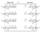
- FIG. 4A Shown are eight memory chips 50 0 - 50 7 together representing a byte lane of data (DQ 0 -DQ 7 ) from the memory module PCB on which the chips 50 x are mounted (not shown for clarity). Depicted for each chip 50 x is the data out path, which comprises an internal data out signal 52 , a standard output buffer 56 , a bond pad 58 , and a bond wire 60 that ultimately connects to the lead frame of the package in which the chips 50 x are positioned (not shown), and ultimately to the various contacts 20 ( FIGS. 1A-B ) on the module 10 .
- the data out path which comprises an internal data out signal 52 , a standard output buffer 56 , a bond pad 58 , and a bond wire 60 that ultimately connects to the lead frame of the package in which the chips 50 x are positioned (not shown), and ultimately to the various contacts 20 ( FIGS. 1A-B ) on the module 10 .
- each of the eight DQ signals on the module 10 is derived from one bit of each of the eight memory chips 50 x . That is to say, it is assume that x1 DRAMs are used. Of course, this need not be the case, and the various data paths comprising the module's byte lane may be integrated on one or more memory chips. For example, each of the nibbles may be provided by four separate outputs on two different memory chips 55 x (shown in dotted lines). More typically, in current-day DDR DRAMs modules, the eight data paths comprising a particular byte lane are all intergraded on one DRAM memory chip 57 , as shown in FIG. 4B .
- FIG. 4B illustrates the utility of the disclosed technique even when a call for data is made to a single integrated circuit).
- the delay circuit 54 can be placed anywhere along the data path, including earlier “up stream” in the chip. Note that this delay circuit 54 does not appear in the later nibble in FIG. 4A or 4 B. Accordingly, when the microprocessor for example calls for data from the byte lane, the earlier nibble will be delayed by the delay circuits 54 by 50 ps, just as the later nibble will be delayed by virtue of the additional length of the top conductors 22 t ( FIG.
- the byte will arrive at the mother board with no or reduced skew.
- This allows the data valid window to be set around the arrival of data at the microprocessor with greater accuracy and buffer, without the need to lengthen any circuit traces on the mother board.
- the data valid signal, DQS may also be delayed if necessary, more specifically if it were provided on the bottom side of the module, although this is unnecessary in the example discussed earlier (see FIG. 2 ).
- FIG. 5A shows a simple way in which the on-chip delay circuit 54 can be fabricated. As shown, delay is introduced simply by providing a series of inverters 62 . Each inverter 62 provides some amount of delay to the internal data out signal 52 . Typically, this delay for a CMOS inverter is on the order of 10-20 ps for current CMOS technologies, and can be easily scaled by adjusting the gate lengths and widths of the NMOS and PMOS transistors which make up the inverter.
- delay circuit 54 of FIG. 5A Even further preferable to the delay circuit 54 of FIG. 5A are delay circuits that are programmable. As applied to the byte lane data skew problem discussed above, programmability is desirable to provide greater flexibility in the type of connectors 18 ( FIG. 1B ) with which the modules can be used. As noted in the Background section, a given module 10 can be used with varying types of connectors 18 , such as 90-degree ( FIG. 1B ) or 0-degree connectors ( FIG. 3 ), and thus a fixed delay circuit 54 would not be optimal were it desired to use the module with either of these types of connector.
- FIG. 4C illustrates the use of programmable delay circuits 54 .
- each output comprising a bit in the byte lane has a delay circuit 54 in its data out path.
- the effect is the same as that shown in FIGS. 4A and 4B , except that now that chips 50 x , 55 x , or 57 can be made uniformly, and then later programmed to address the unique problems of skew present in the byte lane.
- FIG. 5B illustrates a programmable delay circuit 54 .
- inverters 62 are used as the basic delay element, with antifuses (AF) 64 spanning every two inverters 62 .
- the antifuses 64 act as open circuits, and hence a delay of eight inverter stages (e.g., 120 ps) would be introduced if none of the antifuses 64 are programmed; six stages if one of the antifuses are programmed; four stages if two of the antifuses are programmed; two stages if three of the antifuses are programmed; and no delay if all of the antifuses are programmed.
- FIG. 5C achieves this same programming ability, with the need to only program one antifuse to effect a delay between zero to eight inverter stages. As antifuses and methods for programming them are well known in the semiconductor art, the circuitry used to do so is not shown.
- Fuses could also be used, as illustrated in FIGS. 5D and 5E .
- the fuses 66 act as short circuits, and hence no delay would be introduced if none of the fuses 66 are programmed in FIG. 5D ; two inverter stages of delay if one of the fuses are programmed; four stages if two of the fuses are programmed; six stages if three of the fuses are programmed; and eight stages if all of the fuses are programmed.
- FIG. 5E achieves this same programming ability, with the need to only program one fuse to effect a delay between zero to eight inverter stages.
- the fuses 66 may be either programmable by signal (i.e., by the application of a voltage across the fuse), or by light (e.g., by laser ablation).
- a mode register contains various settings used to tailor the operation of the chip.
- the mode register can be programmed using special test modes, usually by activating otherwise standard control signals on the chips or the module in unique sequences. Using such a standard technique, the delay value for each of the delay circuit can be easily programmed. Such programming could occur at the chip level (i.e., before the chips are mounted to a PCB), or at the board level (i.e., after mounting to the module PCB).
- serially-connected inverters 62 is only one way of creating a delayed signal on the earlier nibble.
- many different types of fixed, one-time programmable, or freely programmable delay circuits can be used to achieve the goal of delaying the internal data out signal 52 .
- other logic gates can be used, varying capacitances can be provided to achieve a desired granularity in the delay on the internal data out signal, etc.
- a “mother board” need be only another board for communicating with the memory module. While such a board would typically contain a system microprocessor were the memory module to be used in a traditional computer configuration, this is not strictly necessary. Any board capable of calling the memory module could comprise the mother board, regardless of its configuration and function.
Abstract
Description
Claims (45)
Priority Applications (2)
| Application Number | Priority Date | Filing Date | Title |
|---|---|---|---|
| US13/281,643 US8631267B2 (en) | 2005-05-09 | 2011-10-26 | Adjustable byte lane offset for memory module to reduce skew |
| US14/153,552 US20140129869A1 (en) | 2005-05-09 | 2014-01-13 | Adjustable Byte Lane Offset For Memory Module to Reduce Skew |
Applications Claiming Priority (3)
| Application Number | Priority Date | Filing Date | Title |
|---|---|---|---|
| US11/124,744 US7457978B2 (en) | 2005-05-09 | 2005-05-09 | Adjustable byte lane offset for memory module to reduce skew |
| US12/265,265 US8065551B2 (en) | 2005-05-09 | 2008-11-05 | Adjustable byte lane offset for memory module to reduce skew |
| US13/281,643 US8631267B2 (en) | 2005-05-09 | 2011-10-26 | Adjustable byte lane offset for memory module to reduce skew |
Related Parent Applications (2)
| Application Number | Title | Priority Date | Filing Date |
|---|---|---|---|
| US11/124,744 Continuation US7457978B2 (en) | 2005-05-09 | 2005-05-09 | Adjustable byte lane offset for memory module to reduce skew |
| US12/265,265 Continuation US8065551B2 (en) | 2005-05-09 | 2008-11-05 | Adjustable byte lane offset for memory module to reduce skew |
Related Child Applications (1)
| Application Number | Title | Priority Date | Filing Date |
|---|---|---|---|
| US14/153,552 Continuation US20140129869A1 (en) | 2005-05-09 | 2014-01-13 | Adjustable Byte Lane Offset For Memory Module to Reduce Skew |
Publications (2)
| Publication Number | Publication Date |
|---|---|
| US20120047388A1 US20120047388A1 (en) | 2012-02-23 |
| US8631267B2 true US8631267B2 (en) | 2014-01-14 |
Family
ID=37395343
Family Applications (4)
| Application Number | Title | Priority Date | Filing Date |
|---|---|---|---|
| US11/124,744 Active 2026-06-15 US7457978B2 (en) | 2005-05-09 | 2005-05-09 | Adjustable byte lane offset for memory module to reduce skew |
| US12/265,265 Active 2026-06-22 US8065551B2 (en) | 2005-05-09 | 2008-11-05 | Adjustable byte lane offset for memory module to reduce skew |
| US13/281,643 Active US8631267B2 (en) | 2005-05-09 | 2011-10-26 | Adjustable byte lane offset for memory module to reduce skew |
| US14/153,552 Abandoned US20140129869A1 (en) | 2005-05-09 | 2014-01-13 | Adjustable Byte Lane Offset For Memory Module to Reduce Skew |
Family Applications Before (2)
| Application Number | Title | Priority Date | Filing Date |
|---|---|---|---|
| US11/124,744 Active 2026-06-15 US7457978B2 (en) | 2005-05-09 | 2005-05-09 | Adjustable byte lane offset for memory module to reduce skew |
| US12/265,265 Active 2026-06-22 US8065551B2 (en) | 2005-05-09 | 2008-11-05 | Adjustable byte lane offset for memory module to reduce skew |
Family Applications After (1)
| Application Number | Title | Priority Date | Filing Date |
|---|---|---|---|
| US14/153,552 Abandoned US20140129869A1 (en) | 2005-05-09 | 2014-01-13 | Adjustable Byte Lane Offset For Memory Module to Reduce Skew |
Country Status (1)
| Country | Link |
|---|---|
| US (4) | US7457978B2 (en) |
Cited By (2)
| Publication number | Priority date | Publication date | Assignee | Title |
|---|---|---|---|---|
| US9640278B1 (en) | 2015-12-10 | 2017-05-02 | Integrated Device Technology, Inc. | Testability/manufacturing method to adjust output skew timing |
| US9666263B2 (en) | 2015-10-07 | 2017-05-30 | Samsung Electronics Co., Ltd. | DIMM SSD SoC DRAM byte lane skewing |
Families Citing this family (17)
| Publication number | Priority date | Publication date | Assignee | Title |
|---|---|---|---|---|
| US9286198B2 (en) | 2005-04-21 | 2016-03-15 | Violin Memory | Method and system for storage of data in non-volatile media |
| US9582449B2 (en) | 2005-04-21 | 2017-02-28 | Violin Memory, Inc. | Interconnection system |
| US9384818B2 (en) | 2005-04-21 | 2016-07-05 | Violin Memory | Memory power management |
| US8112655B2 (en) | 2005-04-21 | 2012-02-07 | Violin Memory, Inc. | Mesosynchronous data bus apparatus and method of data transmission |
| CA2597692A1 (en) | 2005-04-21 | 2006-11-02 | Violin Memory, Inc. | Interconnection system |
| US8452929B2 (en) | 2005-04-21 | 2013-05-28 | Violin Memory Inc. | Method and system for storage of data in non-volatile media |
| US7457978B2 (en) | 2005-05-09 | 2008-11-25 | Micron Technology, Inc. | Adjustable byte lane offset for memory module to reduce skew |
| US8028186B2 (en) | 2006-10-23 | 2011-09-27 | Violin Memory, Inc. | Skew management in an interconnection system |
| US7873857B2 (en) * | 2007-01-18 | 2011-01-18 | Qimonda Ag | Multi-component module fly-by output alignment arrangement and method |
| US8717057B2 (en) * | 2008-06-27 | 2014-05-06 | Qualcomm Incorporated | Integrated tester chip using die packaging technologies |
| KR20120133151A (en) * | 2011-05-30 | 2012-12-10 | 삼성전자주식회사 | Display Driver Integrated Circuit having zigzag-type spreading output driving scheme, Display Device including the same and Method for driving the display device |
| US9158330B1 (en) * | 2011-11-15 | 2015-10-13 | Marvell Israel (M.I.S.L) Ltd. | Apparatus and method to compensate for data skew for multiple memory devices and adjust delay for individual data lines based on an optimized critical window |
| EP3058571A1 (en) | 2013-10-15 | 2016-08-24 | Rambus Inc. | Load reduced memory module |
| WO2015124255A1 (en) * | 2014-02-21 | 2015-08-27 | Merck Patent Gmbh | Materials for organic electroluminescent devices |
| KR20180085192A (en) * | 2017-01-18 | 2018-07-26 | 에스케이하이닉스 주식회사 | System including hot plug module and memory module |
| US10395702B1 (en) * | 2018-05-11 | 2019-08-27 | Micron Technology, Inc. | Memory device with a clocking mechanism |
| US11714707B2 (en) * | 2021-04-15 | 2023-08-01 | Dell Products L.P. | DDR5 crosstalk mitigation through agressor misalignment |
Citations (36)
| Publication number | Priority date | Publication date | Assignee | Title |
|---|---|---|---|---|
| US5406518A (en) | 1994-02-08 | 1995-04-11 | Industrial Technology Research Institute | Variable length delay circuit utilizing an integrated memory device with multiple-input and multiple-output configuration |
| US5703815A (en) | 1995-03-24 | 1997-12-30 | Nec Corporation | High-speed semiconductor memory system |
| US5727021A (en) | 1996-04-03 | 1998-03-10 | Teradyne, Inc. | Apparatus and method for providing a programmable delay with low fixed delay |
| US5946712A (en) | 1997-06-04 | 1999-08-31 | Oak Technology, Inc. | Apparatus and method for reading data from synchronous memory |
| US6031847A (en) | 1997-07-01 | 2000-02-29 | Silicon Graphics, Inc | Method and system for deskewing parallel bus channels |
| US6150863A (en) | 1998-04-01 | 2000-11-21 | Xilinx, Inc. | User-controlled delay circuit for a programmable logic device |
| US6167528A (en) | 1995-12-21 | 2000-12-26 | Cypress Semiconductor | Programmably timed storage element for integrated circuit input/output |
| US20020091958A1 (en) | 2001-01-05 | 2002-07-11 | Micron Technology, Inc. | Method and apparatus for improving output skew |
| US6464540B1 (en) | 1998-06-19 | 2002-10-15 | Nec Corporation | Connector unit having signal paths substantially equal to one another in delay time of signals transmitted therethrough |
| US6484299B1 (en) | 2000-07-07 | 2002-11-19 | Micron Technology, Inc. | Method and apparatus for PCB array with compensated signal propagation |
| US20020174313A1 (en) | 2001-05-16 | 2002-11-21 | Justus Kuhn | Method of matching different signal propagation times between a controller and at least two processing units, and a computer system |
| US20020181214A1 (en) | 2001-05-31 | 2002-12-05 | Levy Paul S. | Module having integrated circuit packages coupled to multiple sides with package types selected based on inductance of leads to couple the module to another component |
| US20020199126A1 (en) | 2001-06-26 | 2002-12-26 | Volk Andrew M. | Method and system for reducing the effects of simultaneously switching outputs |
| US20030046618A1 (en) | 2001-08-29 | 2003-03-06 | Collins Hansel A. | Relative dynamic skew compensation of parallel data lines |
| US20030112827A1 (en) | 2001-12-13 | 2003-06-19 | International Business Machines Corporation | Method and apparatus for deskewing parallel serial data channels using asynchronous elastic buffers |
| US6629222B1 (en) | 1999-07-13 | 2003-09-30 | Micron Technology Inc. | Apparatus for synchronizing strobe and data signals received from a RAM |
| US6708238B1 (en) | 2001-01-19 | 2004-03-16 | Sun Microsystems, Inc. | Input/output cell with a programmable delay element |
| US6763444B2 (en) | 2001-05-08 | 2004-07-13 | Micron Technology, Inc. | Read/write timing calibration of a memory array using a row or a redundant row |
| US6832277B2 (en) | 2001-08-02 | 2004-12-14 | Sun Microsystems, Inc. | Method and apparatus for transmitting data that utilizes delay elements to reduce capacitive coupling |
| US20050005184A1 (en) | 2003-03-26 | 2005-01-06 | Lindt Paul Georg | Method for measuring and compensating skews of data transmission lines |
| US20050047187A1 (en) | 2003-08-29 | 2005-03-03 | Min-Sang Park | Integrated circuit memory devices reducing propagation delay differences between signals transmitted to separate spaced-apart memory blocks therein |
| US20050057987A1 (en) | 2003-09-11 | 2005-03-17 | Matsushita Electric Industrial Co., Ltd. | Semiconductor device |
| US20050057978A1 (en) | 2001-11-26 | 2005-03-17 | Stubbs Eric T. | Per-bit set-up and hold time adjustment for double-data rate synchronous DRAM |
| US6887336B2 (en) | 2001-08-30 | 2005-05-03 | Micron Technology, Inc. | Method for fabricating a CMP pad having isolated pockets of continuous porosity |
| US20050226061A1 (en) | 2004-03-30 | 2005-10-13 | Ki-Chon Park | Semiconductor memory device with reduced skew on data line |
| US6963989B1 (en) | 2000-05-22 | 2005-11-08 | Micron Technology, Inc. | Method and apparatus for adjusting data hold timing of an output circuit |
| US6968436B2 (en) | 2000-10-03 | 2005-11-22 | Fujitsu Limited | Memory controller that controls supply timing of read data |
| US6998892B1 (en) | 2002-02-13 | 2006-02-14 | Rambus Inc. | Method and apparatus for accommodating delay variations among multiple signals |
| US7039822B2 (en) | 2003-02-27 | 2006-05-02 | Promos Technologies Inc. | Integrated circuit memory architecture with selectively offset data and address delays to minimize skew and provide synchronization of signals at the input/output section |
| US7051225B2 (en) | 2002-05-22 | 2006-05-23 | Elpida Memory Inc. | Memory system, module and register |
| US7079446B2 (en) | 2004-05-21 | 2006-07-18 | Integrated Device Technology, Inc. | DRAM interface circuits having enhanced skew, slew rate and impedance control |
| US20060164909A1 (en) | 2005-01-24 | 2006-07-27 | International Business Machines Corporation | System, method and storage medium for providing programmable delay chains for a memory system |
| US7089509B2 (en) | 2002-12-23 | 2006-08-08 | Sun Microsystems, Inc. | Controlling the propagation of a control signal by means of variable I/O delay compensation using a programmable delay circuit and detection sequence |
| US7193910B2 (en) | 2000-08-25 | 2007-03-20 | Micron Technology, Inc. | Adjustable timing circuit of an integrated circuit |
| US7281950B2 (en) | 2004-09-29 | 2007-10-16 | Fci Americas Technology, Inc. | High speed connectors that minimize signal skew and crosstalk |
| US7457978B2 (en) | 2005-05-09 | 2008-11-25 | Micron Technology, Inc. | Adjustable byte lane offset for memory module to reduce skew |
Family Cites Families (7)
| Publication number | Priority date | Publication date | Assignee | Title |
|---|---|---|---|---|
| US5272664A (en) * | 1993-04-21 | 1993-12-21 | Silicon Graphics, Inc. | High memory capacity DRAM SIMM |
| US6745275B2 (en) * | 2000-01-25 | 2004-06-01 | Via Technologies, Inc. | Feedback system for accomodating different memory module loading |
| WO2002025296A2 (en) * | 2000-09-22 | 2002-03-28 | Don Mccord | Method and system for wafer and device-level testing of an integrated circuit |
| US6466008B1 (en) * | 2000-10-06 | 2002-10-15 | Hewlett-Packard Company | Method for matching the lengths of signal traces |
| US6751113B2 (en) * | 2002-03-07 | 2004-06-15 | Netlist, Inc. | Arrangement of integrated circuits in a memory module |
| US7003686B2 (en) * | 2002-05-20 | 2006-02-21 | Hitachi Ltd. | Interface circuit |
| JP4290537B2 (en) * | 2003-11-26 | 2009-07-08 | 株式会社ルネサステクノロジ | Semiconductor device |
-
2005
- 2005-05-09 US US11/124,744 patent/US7457978B2/en active Active
-
2008
- 2008-11-05 US US12/265,265 patent/US8065551B2/en active Active
-
2011
- 2011-10-26 US US13/281,643 patent/US8631267B2/en active Active
-
2014
- 2014-01-13 US US14/153,552 patent/US20140129869A1/en not_active Abandoned
Patent Citations (42)
| Publication number | Priority date | Publication date | Assignee | Title |
|---|---|---|---|---|
| US5406518A (en) | 1994-02-08 | 1995-04-11 | Industrial Technology Research Institute | Variable length delay circuit utilizing an integrated memory device with multiple-input and multiple-output configuration |
| US5703815A (en) | 1995-03-24 | 1997-12-30 | Nec Corporation | High-speed semiconductor memory system |
| US6167528A (en) | 1995-12-21 | 2000-12-26 | Cypress Semiconductor | Programmably timed storage element for integrated circuit input/output |
| US5727021A (en) | 1996-04-03 | 1998-03-10 | Teradyne, Inc. | Apparatus and method for providing a programmable delay with low fixed delay |
| US5946712A (en) | 1997-06-04 | 1999-08-31 | Oak Technology, Inc. | Apparatus and method for reading data from synchronous memory |
| US6031847A (en) | 1997-07-01 | 2000-02-29 | Silicon Graphics, Inc | Method and system for deskewing parallel bus channels |
| US6150863A (en) | 1998-04-01 | 2000-11-21 | Xilinx, Inc. | User-controlled delay circuit for a programmable logic device |
| US6464540B1 (en) | 1998-06-19 | 2002-10-15 | Nec Corporation | Connector unit having signal paths substantially equal to one another in delay time of signals transmitted therethrough |
| US6629222B1 (en) | 1999-07-13 | 2003-09-30 | Micron Technology Inc. | Apparatus for synchronizing strobe and data signals received from a RAM |
| US6963989B1 (en) | 2000-05-22 | 2005-11-08 | Micron Technology, Inc. | Method and apparatus for adjusting data hold timing of an output circuit |
| US6484299B1 (en) | 2000-07-07 | 2002-11-19 | Micron Technology, Inc. | Method and apparatus for PCB array with compensated signal propagation |
| US7193910B2 (en) | 2000-08-25 | 2007-03-20 | Micron Technology, Inc. | Adjustable timing circuit of an integrated circuit |
| US6968436B2 (en) | 2000-10-03 | 2005-11-22 | Fujitsu Limited | Memory controller that controls supply timing of read data |
| US20020091958A1 (en) | 2001-01-05 | 2002-07-11 | Micron Technology, Inc. | Method and apparatus for improving output skew |
| US6889336B2 (en) | 2001-01-05 | 2005-05-03 | Micron Technology, Inc. | Apparatus for improving output skew for synchronous integrate circuits has delay circuit for generating unique clock signal by applying programmable delay to delayed clock signal |
| US7272742B2 (en) | 2001-01-05 | 2007-09-18 | Micron Technology, Inc. | Method and apparatus for improving output skew for synchronous integrated circuits |
| US6708238B1 (en) | 2001-01-19 | 2004-03-16 | Sun Microsystems, Inc. | Input/output cell with a programmable delay element |
| US6763444B2 (en) | 2001-05-08 | 2004-07-13 | Micron Technology, Inc. | Read/write timing calibration of a memory array using a row or a redundant row |
| US20020174313A1 (en) | 2001-05-16 | 2002-11-21 | Justus Kuhn | Method of matching different signal propagation times between a controller and at least two processing units, and a computer system |
| US20020181214A1 (en) | 2001-05-31 | 2002-12-05 | Levy Paul S. | Module having integrated circuit packages coupled to multiple sides with package types selected based on inductance of leads to couple the module to another component |
| US20020199126A1 (en) | 2001-06-26 | 2002-12-26 | Volk Andrew M. | Method and system for reducing the effects of simultaneously switching outputs |
| US6971040B2 (en) | 2001-06-26 | 2005-11-29 | Intel Corporation | Method and system for reducing the effects of simultaneously switching outputs |
| US6832277B2 (en) | 2001-08-02 | 2004-12-14 | Sun Microsystems, Inc. | Method and apparatus for transmitting data that utilizes delay elements to reduce capacitive coupling |
| US20030046618A1 (en) | 2001-08-29 | 2003-03-06 | Collins Hansel A. | Relative dynamic skew compensation of parallel data lines |
| US6887336B2 (en) | 2001-08-30 | 2005-05-03 | Micron Technology, Inc. | Method for fabricating a CMP pad having isolated pockets of continuous porosity |
| US20050057978A1 (en) | 2001-11-26 | 2005-03-17 | Stubbs Eric T. | Per-bit set-up and hold time adjustment for double-data rate synchronous DRAM |
| US20030112827A1 (en) | 2001-12-13 | 2003-06-19 | International Business Machines Corporation | Method and apparatus for deskewing parallel serial data channels using asynchronous elastic buffers |
| US6998892B1 (en) | 2002-02-13 | 2006-02-14 | Rambus Inc. | Method and apparatus for accommodating delay variations among multiple signals |
| US7051225B2 (en) | 2002-05-22 | 2006-05-23 | Elpida Memory Inc. | Memory system, module and register |
| US7089509B2 (en) | 2002-12-23 | 2006-08-08 | Sun Microsystems, Inc. | Controlling the propagation of a control signal by means of variable I/O delay compensation using a programmable delay circuit and detection sequence |
| US7039822B2 (en) | 2003-02-27 | 2006-05-02 | Promos Technologies Inc. | Integrated circuit memory architecture with selectively offset data and address delays to minimize skew and provide synchronization of signals at the input/output section |
| US20050005184A1 (en) | 2003-03-26 | 2005-01-06 | Lindt Paul Georg | Method for measuring and compensating skews of data transmission lines |
| US7110276B2 (en) | 2003-08-29 | 2006-09-19 | Samsung Electronics Co., Ltd. | Integrated circuit memory devices reducing propagation delay differences between signals transmitted to separate spaced-apart memory blocks therein |
| US20050047187A1 (en) | 2003-08-29 | 2005-03-03 | Min-Sang Park | Integrated circuit memory devices reducing propagation delay differences between signals transmitted to separate spaced-apart memory blocks therein |
| US20050057987A1 (en) | 2003-09-11 | 2005-03-17 | Matsushita Electric Industrial Co., Ltd. | Semiconductor device |
| US20050226061A1 (en) | 2004-03-30 | 2005-10-13 | Ki-Chon Park | Semiconductor memory device with reduced skew on data line |
| US7079446B2 (en) | 2004-05-21 | 2006-07-18 | Integrated Device Technology, Inc. | DRAM interface circuits having enhanced skew, slew rate and impedance control |
| US7281950B2 (en) | 2004-09-29 | 2007-10-16 | Fci Americas Technology, Inc. | High speed connectors that minimize signal skew and crosstalk |
| US20060164909A1 (en) | 2005-01-24 | 2006-07-27 | International Business Machines Corporation | System, method and storage medium for providing programmable delay chains for a memory system |
| US7457978B2 (en) | 2005-05-09 | 2008-11-25 | Micron Technology, Inc. | Adjustable byte lane offset for memory module to reduce skew |
| US20090055675A1 (en) | 2005-05-09 | 2009-02-26 | Micron Technology, Inc. | Adjustable Byte Lane Offset For Memory Module To Reduce Skew |
| US8065551B2 (en) | 2005-05-09 | 2011-11-22 | Micron Technology, Inc. | Adjustable byte lane offset for memory module to reduce skew |
Non-Patent Citations (9)
Cited By (2)
| Publication number | Priority date | Publication date | Assignee | Title |
|---|---|---|---|---|
| US9666263B2 (en) | 2015-10-07 | 2017-05-30 | Samsung Electronics Co., Ltd. | DIMM SSD SoC DRAM byte lane skewing |
| US9640278B1 (en) | 2015-12-10 | 2017-05-02 | Integrated Device Technology, Inc. | Testability/manufacturing method to adjust output skew timing |
Also Published As
| Publication number | Publication date |
|---|---|
| US7457978B2 (en) | 2008-11-25 |
| US8065551B2 (en) | 2011-11-22 |
| US20090055675A1 (en) | 2009-02-26 |
| US20120047388A1 (en) | 2012-02-23 |
| US20140129869A1 (en) | 2014-05-08 |
| US20060253721A1 (en) | 2006-11-09 |
Similar Documents
| Publication | Publication Date | Title |
|---|---|---|
| US8631267B2 (en) | Adjustable byte lane offset for memory module to reduce skew | |
| US20200349991A1 (en) | Memory control component with inter-rank skew tolerance | |
| US6347394B1 (en) | Buffering circuit embedded in an integrated circuit device module used for buffering clocks and other input signals | |
| US6446158B1 (en) | Memory system using FET switches to select memory banks | |
| US7426145B2 (en) | Synchronous semiconductor memory device having on-die termination circuit and on-die termination method | |
| US7634677B2 (en) | Circuit and method for outputting aligned strobe signal and parallel data signal | |
| US6653877B2 (en) | Semiconductor device capable of internally adjusting delayed amount of a clock signal | |
| WO1999046687A1 (en) | Data transmitter | |
| US7323789B2 (en) | Multiple chip package and IC chips | |
| US20080285375A1 (en) | Semiconductor device, module including the semiconductor device, and system including the module | |
| US7539826B2 (en) | System, device, and method for improved mirror mode operation of a semiconductor memory device | |
| US7068064B1 (en) | Memory module with dynamic termination using bus switches timed by memory clock and chip select | |
| US7894260B2 (en) | Synchronous semiconductor memory device having on-die termination circuit and on-die termination method | |
| US20060215467A1 (en) | Method of increasing data setup and hold margin in case of non-symmetrical PVT | |
| US6376869B1 (en) | Semiconductor device | |
| KR100586572B1 (en) | Improved high speed data capture circuit for a digital device | |
| US6556051B2 (en) | Apparatus for providing both supports including synchronous dynamic random access memory (SDRAM) module and double data rate (DDR) DRAM module | |
| KR100546271B1 (en) | Semiconductor devices | |
| US6448849B1 (en) | Semiconductor devices including a switch mounted thereon and a module loaded with the same | |
| JPH1011971A (en) | Semiconductor memory device | |
| KR20020005828A (en) | Generation circuit of input data for command decoding circuit, for improving setup/hold margin |
Legal Events
| Date | Code | Title | Description |
|---|---|---|---|
| AS | Assignment |
Owner name: MICRON TECHNOLOGY, INC., IDAHO Free format text: ASSIGNMENT OF ASSIGNORS INTEREST;ASSIGNOR:JOHNSON, CHRISTOPHER S.;REEL/FRAME:027123/0339 Effective date: 20050505 |
|
| FEPP | Fee payment procedure |
Free format text: PAYOR NUMBER ASSIGNED (ORIGINAL EVENT CODE: ASPN); ENTITY STATUS OF PATENT OWNER: LARGE ENTITY |
|
| STCF | Information on status: patent grant |
Free format text: PATENTED CASE |
|
| AS | Assignment |
Owner name: U.S. BANK NATIONAL ASSOCIATION, AS COLLATERAL AGENT, CALIFORNIA Free format text: SECURITY INTEREST;ASSIGNOR:MICRON TECHNOLOGY, INC.;REEL/FRAME:038669/0001 Effective date: 20160426 Owner name: U.S. BANK NATIONAL ASSOCIATION, AS COLLATERAL AGEN Free format text: SECURITY INTEREST;ASSIGNOR:MICRON TECHNOLOGY, INC.;REEL/FRAME:038669/0001 Effective date: 20160426 |
|
| AS | Assignment |
Owner name: MORGAN STANLEY SENIOR FUNDING, INC., AS COLLATERAL AGENT, MARYLAND Free format text: PATENT SECURITY AGREEMENT;ASSIGNOR:MICRON TECHNOLOGY, INC.;REEL/FRAME:038954/0001 Effective date: 20160426 Owner name: MORGAN STANLEY SENIOR FUNDING, INC., AS COLLATERAL Free format text: PATENT SECURITY AGREEMENT;ASSIGNOR:MICRON TECHNOLOGY, INC.;REEL/FRAME:038954/0001 Effective date: 20160426 |
|
| AS | Assignment |
Owner name: U.S. BANK NATIONAL ASSOCIATION, AS COLLATERAL AGENT, CALIFORNIA Free format text: CORRECTIVE ASSIGNMENT TO CORRECT THE REPLACE ERRONEOUSLY FILED PATENT #7358718 WITH THE CORRECT PATENT #7358178 PREVIOUSLY RECORDED ON REEL 038669 FRAME 0001. ASSIGNOR(S) HEREBY CONFIRMS THE SECURITY INTEREST;ASSIGNOR:MICRON TECHNOLOGY, INC.;REEL/FRAME:043079/0001 Effective date: 20160426 Owner name: U.S. BANK NATIONAL ASSOCIATION, AS COLLATERAL AGEN Free format text: CORRECTIVE ASSIGNMENT TO CORRECT THE REPLACE ERRONEOUSLY FILED PATENT #7358718 WITH THE CORRECT PATENT #7358178 PREVIOUSLY RECORDED ON REEL 038669 FRAME 0001. ASSIGNOR(S) HEREBY CONFIRMS THE SECURITY INTEREST;ASSIGNOR:MICRON TECHNOLOGY, INC.;REEL/FRAME:043079/0001 Effective date: 20160426 |
|
| FPAY | Fee payment |
Year of fee payment: 4 |
|
| AS | Assignment |
Owner name: JPMORGAN CHASE BANK, N.A., AS COLLATERAL AGENT, ILLINOIS Free format text: SECURITY INTEREST;ASSIGNORS:MICRON TECHNOLOGY, INC.;MICRON SEMICONDUCTOR PRODUCTS, INC.;REEL/FRAME:047540/0001 Effective date: 20180703 Owner name: JPMORGAN CHASE BANK, N.A., AS COLLATERAL AGENT, IL Free format text: SECURITY INTEREST;ASSIGNORS:MICRON TECHNOLOGY, INC.;MICRON SEMICONDUCTOR PRODUCTS, INC.;REEL/FRAME:047540/0001 Effective date: 20180703 |
|
| AS | Assignment |
Owner name: MICRON TECHNOLOGY, INC., IDAHO Free format text: RELEASE BY SECURED PARTY;ASSIGNOR:U.S. BANK NATIONAL ASSOCIATION, AS COLLATERAL AGENT;REEL/FRAME:047243/0001 Effective date: 20180629 |
|
| AS | Assignment |
Owner name: MICRON TECHNOLOGY, INC., IDAHO Free format text: RELEASE BY SECURED PARTY;ASSIGNOR:MORGAN STANLEY SENIOR FUNDING, INC., AS COLLATERAL AGENT;REEL/FRAME:050937/0001 Effective date: 20190731 |
|
| AS | Assignment |
Owner name: MICRON TECHNOLOGY, INC., IDAHO Free format text: RELEASE BY SECURED PARTY;ASSIGNOR:JPMORGAN CHASE BANK, N.A., AS COLLATERAL AGENT;REEL/FRAME:051028/0001 Effective date: 20190731 Owner name: MICRON SEMICONDUCTOR PRODUCTS, INC., IDAHO Free format text: RELEASE BY SECURED PARTY;ASSIGNOR:JPMORGAN CHASE BANK, N.A., AS COLLATERAL AGENT;REEL/FRAME:051028/0001 Effective date: 20190731 |
|
| MAFP | Maintenance fee payment |
Free format text: PAYMENT OF MAINTENANCE FEE, 8TH YEAR, LARGE ENTITY (ORIGINAL EVENT CODE: M1552); ENTITY STATUS OF PATENT OWNER: LARGE ENTITY Year of fee payment: 8 |