US8623700B1 - Inter-chip communication - Google Patents
Inter-chip communication Download PDFInfo
- Publication number
- US8623700B1 US8623700B1 US11/599,283 US59928306A US8623700B1 US 8623700 B1 US8623700 B1 US 8623700B1 US 59928306 A US59928306 A US 59928306A US 8623700 B1 US8623700 B1 US 8623700B1
- Authority
- US
- United States
- Prior art keywords
- microchip
- interconnect
- nodules
- microchips
- interconnect nodules
- Prior art date
- Legal status (The legal status is an assumption and is not a legal conclusion. Google has not performed a legal analysis and makes no representation as to the accuracy of the status listed.)
- Active, expires
Links
- 238000004891 communication Methods 0.000 title claims description 30
- 238000004806 packaging method and process Methods 0.000 claims abstract description 105
- 238000000034 method Methods 0.000 claims abstract description 73
- 239000004065 semiconductor Substances 0.000 claims description 40
- 238000004519 manufacturing process Methods 0.000 claims description 20
- 239000004020 conductor Substances 0.000 claims description 16
- 238000003466 welding Methods 0.000 claims description 14
- 125000006850 spacer group Chemical group 0.000 claims description 9
- 238000000151 deposition Methods 0.000 claims description 7
- 230000013011 mating Effects 0.000 claims description 2
- 239000011800 void material Substances 0.000 claims 6
- 235000012431 wafers Nutrition 0.000 description 64
- 239000002184 metal Substances 0.000 description 26
- 229910052751 metal Inorganic materials 0.000 description 26
- 230000008569 process Effects 0.000 description 26
- 239000000463 material Substances 0.000 description 17
- 238000005516 engineering process Methods 0.000 description 15
- 230000010354 integration Effects 0.000 description 13
- 230000003287 optical effect Effects 0.000 description 10
- 238000000708 deep reactive-ion etching Methods 0.000 description 9
- 238000005530 etching Methods 0.000 description 9
- 239000011295 pitch Substances 0.000 description 9
- 238000013459 approach Methods 0.000 description 8
- XUIMIQQOPSSXEZ-UHFFFAOYSA-N Silicon Chemical compound [Si] XUIMIQQOPSSXEZ-UHFFFAOYSA-N 0.000 description 7
- 230000008901 benefit Effects 0.000 description 7
- 230000033001 locomotion Effects 0.000 description 7
- 238000001000 micrograph Methods 0.000 description 7
- 229910052710 silicon Inorganic materials 0.000 description 7
- 239000010703 silicon Substances 0.000 description 7
- 239000000126 substance Substances 0.000 description 7
- 239000000758 substrate Substances 0.000 description 7
- 239000011248 coating agent Substances 0.000 description 6
- 238000000576 coating method Methods 0.000 description 6
- 238000010586 diagram Methods 0.000 description 6
- 230000008030 elimination Effects 0.000 description 6
- 238000003379 elimination reaction Methods 0.000 description 6
- 238000013461 design Methods 0.000 description 5
- 230000006870 function Effects 0.000 description 5
- 238000005498 polishing Methods 0.000 description 5
- 230000009467 reduction Effects 0.000 description 5
- 238000000926 separation method Methods 0.000 description 5
- RYGMFSIKBFXOCR-UHFFFAOYSA-N Copper Chemical compound [Cu] RYGMFSIKBFXOCR-UHFFFAOYSA-N 0.000 description 4
- 229910000577 Silicon-germanium Inorganic materials 0.000 description 4
- 229910052802 copper Inorganic materials 0.000 description 4
- 239000010949 copper Substances 0.000 description 4
- PCHJSUWPFVWCPO-UHFFFAOYSA-N gold Chemical compound [Au] PCHJSUWPFVWCPO-UHFFFAOYSA-N 0.000 description 4
- 229910052737 gold Inorganic materials 0.000 description 4
- 239000010931 gold Substances 0.000 description 4
- 235000019589 hardness Nutrition 0.000 description 4
- 238000012856 packing Methods 0.000 description 4
- 238000007747 plating Methods 0.000 description 4
- 230000001154 acute effect Effects 0.000 description 3
- 239000013043 chemical agent Substances 0.000 description 3
- 230000000295 complement effect Effects 0.000 description 3
- 238000001816 cooling Methods 0.000 description 3
- 238000001514 detection method Methods 0.000 description 3
- 239000003989 dielectric material Substances 0.000 description 3
- 239000012528 membrane Substances 0.000 description 3
- 150000002739 metals Chemical class 0.000 description 3
- 230000006855 networking Effects 0.000 description 3
- 230000005693 optoelectronics Effects 0.000 description 3
- 238000012545 processing Methods 0.000 description 3
- 229910000679 solder Inorganic materials 0.000 description 3
- 238000012546 transfer Methods 0.000 description 3
- 239000003990 capacitor Substances 0.000 description 2
- 230000008878 coupling Effects 0.000 description 2
- 238000010168 coupling process Methods 0.000 description 2
- 238000005859 coupling reaction Methods 0.000 description 2
- 238000005520 cutting process Methods 0.000 description 2
- 230000008021 deposition Effects 0.000 description 2
- 238000007772 electroless plating Methods 0.000 description 2
- 238000012986 modification Methods 0.000 description 2
- 230000004048 modification Effects 0.000 description 2
- 239000013307 optical fiber Substances 0.000 description 2
- 230000003647 oxidation Effects 0.000 description 2
- 238000007254 oxidation reaction Methods 0.000 description 2
- 238000000623 plasma-assisted chemical vapour deposition Methods 0.000 description 2
- 230000035755 proliferation Effects 0.000 description 2
- 238000004088 simulation Methods 0.000 description 2
- 230000000930 thermomechanical effect Effects 0.000 description 2
- 238000005493 welding type Methods 0.000 description 2
- 229910001218 Gallium arsenide Inorganic materials 0.000 description 1
- 229910045601 alloy Inorganic materials 0.000 description 1
- 239000000956 alloy Substances 0.000 description 1
- 238000004458 analytical method Methods 0.000 description 1
- 238000003491 array Methods 0.000 description 1
- 230000005540 biological transmission Effects 0.000 description 1
- 230000007423 decrease Effects 0.000 description 1
- 230000003247 decreasing effect Effects 0.000 description 1
- 230000001934 delay Effects 0.000 description 1
- 238000011982 device technology Methods 0.000 description 1
- 229910003460 diamond Inorganic materials 0.000 description 1
- 239000010432 diamond Substances 0.000 description 1
- 230000005672 electromagnetic field Effects 0.000 description 1
- 238000010894 electron beam technology Methods 0.000 description 1
- 230000009969 flowable effect Effects 0.000 description 1
- 239000012530 fluid Substances 0.000 description 1
- 238000000227 grinding Methods 0.000 description 1
- 230000017525 heat dissipation Effects 0.000 description 1
- 230000036039 immunity Effects 0.000 description 1
- 238000010884 ion-beam technique Methods 0.000 description 1
- 239000007788 liquid Substances 0.000 description 1
- 238000001465 metallisation Methods 0.000 description 1
- 238000003801 milling Methods 0.000 description 1
- 150000004767 nitrides Chemical class 0.000 description 1
- 238000005457 optimization Methods 0.000 description 1
- 238000005192 partition Methods 0.000 description 1
- 238000002161 passivation Methods 0.000 description 1
- 230000002093 peripheral effect Effects 0.000 description 1
- 238000000206 photolithography Methods 0.000 description 1
- 210000002381 plasma Anatomy 0.000 description 1
- 238000001020 plasma etching Methods 0.000 description 1
- 239000004033 plastic Substances 0.000 description 1
- 238000004321 preservation Methods 0.000 description 1
- 238000003825 pressing Methods 0.000 description 1
- 230000001953 sensory effect Effects 0.000 description 1
- 239000007787 solid Substances 0.000 description 1
- 238000000638 solvent extraction Methods 0.000 description 1
- 238000004611 spectroscopical analysis Methods 0.000 description 1
- 230000003068 static effect Effects 0.000 description 1
- 238000012360 testing method Methods 0.000 description 1
- 239000002699 waste material Substances 0.000 description 1
- 238000001039 wet etching Methods 0.000 description 1
- IGELFKKMDLGCJO-UHFFFAOYSA-N xenon difluoride Chemical compound F[Xe]F IGELFKKMDLGCJO-UHFFFAOYSA-N 0.000 description 1
Images


Classifications
-
- H—ELECTRICITY
- H01—ELECTRIC ELEMENTS
- H01L—SEMICONDUCTOR DEVICES NOT COVERED BY CLASS H10
- H01L24/00—Arrangements for connecting or disconnecting semiconductor or solid-state bodies; Methods or apparatus related thereto
- H01L24/01—Means for bonding being attached to, or being formed on, the surface to be connected, e.g. chip-to-package, die-attach, "first-level" interconnects; Manufacturing methods related thereto
- H01L24/63—Connectors not provided for in any of the groups H01L24/10 - H01L24/50 and subgroups; Manufacturing methods related thereto
- H01L24/65—Structure, shape, material or disposition of the connectors prior to the connecting process
- H01L24/67—Structure, shape, material or disposition of the connectors prior to the connecting process of a plurality of connectors
-
- H—ELECTRICITY
- H01—ELECTRIC ELEMENTS
- H01L—SEMICONDUCTOR DEVICES NOT COVERED BY CLASS H10
- H01L23/00—Details of semiconductor or other solid state devices
- H01L23/58—Structural electrical arrangements for semiconductor devices not otherwise provided for, e.g. in combination with batteries
- H01L23/60—Protection against electrostatic charges or discharges, e.g. Faraday shields
-
- H—ELECTRICITY
- H01—ELECTRIC ELEMENTS
- H01L—SEMICONDUCTOR DEVICES NOT COVERED BY CLASS H10
- H01L24/00—Arrangements for connecting or disconnecting semiconductor or solid-state bodies; Methods or apparatus related thereto
- H01L24/01—Means for bonding being attached to, or being formed on, the surface to be connected, e.g. chip-to-package, die-attach, "first-level" interconnects; Manufacturing methods related thereto
- H01L24/02—Bonding areas ; Manufacturing methods related thereto
- H01L24/04—Structure, shape, material or disposition of the bonding areas prior to the connecting process
- H01L24/06—Structure, shape, material or disposition of the bonding areas prior to the connecting process of a plurality of bonding areas
-
- H—ELECTRICITY
- H01—ELECTRIC ELEMENTS
- H01L—SEMICONDUCTOR DEVICES NOT COVERED BY CLASS H10
- H01L24/00—Arrangements for connecting or disconnecting semiconductor or solid-state bodies; Methods or apparatus related thereto
- H01L24/01—Means for bonding being attached to, or being formed on, the surface to be connected, e.g. chip-to-package, die-attach, "first-level" interconnects; Manufacturing methods related thereto
- H01L24/10—Bump connectors ; Manufacturing methods related thereto
- H01L24/12—Structure, shape, material or disposition of the bump connectors prior to the connecting process
- H01L24/13—Structure, shape, material or disposition of the bump connectors prior to the connecting process of an individual bump connector
-
- H—ELECTRICITY
- H01—ELECTRIC ELEMENTS
- H01L—SEMICONDUCTOR DEVICES NOT COVERED BY CLASS H10
- H01L24/00—Arrangements for connecting or disconnecting semiconductor or solid-state bodies; Methods or apparatus related thereto
- H01L24/01—Means for bonding being attached to, or being formed on, the surface to be connected, e.g. chip-to-package, die-attach, "first-level" interconnects; Manufacturing methods related thereto
- H01L24/10—Bump connectors ; Manufacturing methods related thereto
- H01L24/15—Structure, shape, material or disposition of the bump connectors after the connecting process
- H01L24/16—Structure, shape, material or disposition of the bump connectors after the connecting process of an individual bump connector
-
- H—ELECTRICITY
- H01—ELECTRIC ELEMENTS
- H01L—SEMICONDUCTOR DEVICES NOT COVERED BY CLASS H10
- H01L24/00—Arrangements for connecting or disconnecting semiconductor or solid-state bodies; Methods or apparatus related thereto
- H01L24/01—Means for bonding being attached to, or being formed on, the surface to be connected, e.g. chip-to-package, die-attach, "first-level" interconnects; Manufacturing methods related thereto
- H01L24/18—High density interconnect [HDI] connectors; Manufacturing methods related thereto
- H01L24/23—Structure, shape, material or disposition of the high density interconnect connectors after the connecting process
- H01L24/24—Structure, shape, material or disposition of the high density interconnect connectors after the connecting process of an individual high density interconnect connector
-
- H—ELECTRICITY
- H01—ELECTRIC ELEMENTS
- H01L—SEMICONDUCTOR DEVICES NOT COVERED BY CLASS H10
- H01L24/00—Arrangements for connecting or disconnecting semiconductor or solid-state bodies; Methods or apparatus related thereto
- H01L24/01—Means for bonding being attached to, or being formed on, the surface to be connected, e.g. chip-to-package, die-attach, "first-level" interconnects; Manufacturing methods related thereto
- H01L24/63—Connectors not provided for in any of the groups H01L24/10 - H01L24/50 and subgroups; Manufacturing methods related thereto
- H01L24/65—Structure, shape, material or disposition of the connectors prior to the connecting process
- H01L24/66—Structure, shape, material or disposition of the connectors prior to the connecting process of an individual connector
-
- H—ELECTRICITY
- H01—ELECTRIC ELEMENTS
- H01L—SEMICONDUCTOR DEVICES NOT COVERED BY CLASS H10
- H01L24/00—Arrangements for connecting or disconnecting semiconductor or solid-state bodies; Methods or apparatus related thereto
- H01L24/71—Means for bonding not being attached to, or not being formed on, the surface to be connected
- H01L24/72—Detachable connecting means consisting of mechanical auxiliary parts connecting the device, e.g. pressure contacts using springs or clips
-
- H—ELECTRICITY
- H01—ELECTRIC ELEMENTS
- H01L—SEMICONDUCTOR DEVICES NOT COVERED BY CLASS H10
- H01L24/00—Arrangements for connecting or disconnecting semiconductor or solid-state bodies; Methods or apparatus related thereto
- H01L24/73—Means for bonding being of different types provided for in two or more of groups H01L24/10, H01L24/18, H01L24/26, H01L24/34, H01L24/42, H01L24/50, H01L24/63, H01L24/71
-
- H—ELECTRICITY
- H01—ELECTRIC ELEMENTS
- H01L—SEMICONDUCTOR DEVICES NOT COVERED BY CLASS H10
- H01L24/00—Arrangements for connecting or disconnecting semiconductor or solid-state bodies; Methods or apparatus related thereto
- H01L24/80—Methods for connecting semiconductor or other solid state bodies using means for bonding being attached to, or being formed on, the surface to be connected
- H01L24/82—Methods for connecting semiconductor or other solid state bodies using means for bonding being attached to, or being formed on, the surface to be connected by forming build-up interconnects at chip-level, e.g. for high density interconnects [HDI]
-
- H—ELECTRICITY
- H01—ELECTRIC ELEMENTS
- H01L—SEMICONDUCTOR DEVICES NOT COVERED BY CLASS H10
- H01L25/00—Assemblies consisting of a plurality of individual semiconductor or other solid state devices ; Multistep manufacturing processes thereof
- H01L25/03—Assemblies consisting of a plurality of individual semiconductor or other solid state devices ; Multistep manufacturing processes thereof all the devices being of a type provided for in the same subgroup of groups H01L27/00 - H01L33/00, or in a single subclass of H10K, H10N, e.g. assemblies of rectifier diodes
- H01L25/04—Assemblies consisting of a plurality of individual semiconductor or other solid state devices ; Multistep manufacturing processes thereof all the devices being of a type provided for in the same subgroup of groups H01L27/00 - H01L33/00, or in a single subclass of H10K, H10N, e.g. assemblies of rectifier diodes the devices not having separate containers
- H01L25/065—Assemblies consisting of a plurality of individual semiconductor or other solid state devices ; Multistep manufacturing processes thereof all the devices being of a type provided for in the same subgroup of groups H01L27/00 - H01L33/00, or in a single subclass of H10K, H10N, e.g. assemblies of rectifier diodes the devices not having separate containers the devices being of a type provided for in group H01L27/00
- H01L25/0652—Assemblies consisting of a plurality of individual semiconductor or other solid state devices ; Multistep manufacturing processes thereof all the devices being of a type provided for in the same subgroup of groups H01L27/00 - H01L33/00, or in a single subclass of H10K, H10N, e.g. assemblies of rectifier diodes the devices not having separate containers the devices being of a type provided for in group H01L27/00 the devices being arranged next and on each other, i.e. mixed assemblies
-
- H—ELECTRICITY
- H01—ELECTRIC ELEMENTS
- H01L—SEMICONDUCTOR DEVICES NOT COVERED BY CLASS H10
- H01L25/00—Assemblies consisting of a plurality of individual semiconductor or other solid state devices ; Multistep manufacturing processes thereof
- H01L25/03—Assemblies consisting of a plurality of individual semiconductor or other solid state devices ; Multistep manufacturing processes thereof all the devices being of a type provided for in the same subgroup of groups H01L27/00 - H01L33/00, or in a single subclass of H10K, H10N, e.g. assemblies of rectifier diodes
- H01L25/04—Assemblies consisting of a plurality of individual semiconductor or other solid state devices ; Multistep manufacturing processes thereof all the devices being of a type provided for in the same subgroup of groups H01L27/00 - H01L33/00, or in a single subclass of H10K, H10N, e.g. assemblies of rectifier diodes the devices not having separate containers
- H01L25/065—Assemblies consisting of a plurality of individual semiconductor or other solid state devices ; Multistep manufacturing processes thereof all the devices being of a type provided for in the same subgroup of groups H01L27/00 - H01L33/00, or in a single subclass of H10K, H10N, e.g. assemblies of rectifier diodes the devices not having separate containers the devices being of a type provided for in group H01L27/00
- H01L25/0655—Assemblies consisting of a plurality of individual semiconductor or other solid state devices ; Multistep manufacturing processes thereof all the devices being of a type provided for in the same subgroup of groups H01L27/00 - H01L33/00, or in a single subclass of H10K, H10N, e.g. assemblies of rectifier diodes the devices not having separate containers the devices being of a type provided for in group H01L27/00 the devices being arranged next to each other
-
- H—ELECTRICITY
- H01—ELECTRIC ELEMENTS
- H01L—SEMICONDUCTOR DEVICES NOT COVERED BY CLASS H10
- H01L25/00—Assemblies consisting of a plurality of individual semiconductor or other solid state devices ; Multistep manufacturing processes thereof
- H01L25/03—Assemblies consisting of a plurality of individual semiconductor or other solid state devices ; Multistep manufacturing processes thereof all the devices being of a type provided for in the same subgroup of groups H01L27/00 - H01L33/00, or in a single subclass of H10K, H10N, e.g. assemblies of rectifier diodes
- H01L25/04—Assemblies consisting of a plurality of individual semiconductor or other solid state devices ; Multistep manufacturing processes thereof all the devices being of a type provided for in the same subgroup of groups H01L27/00 - H01L33/00, or in a single subclass of H10K, H10N, e.g. assemblies of rectifier diodes the devices not having separate containers
- H01L25/065—Assemblies consisting of a plurality of individual semiconductor or other solid state devices ; Multistep manufacturing processes thereof all the devices being of a type provided for in the same subgroup of groups H01L27/00 - H01L33/00, or in a single subclass of H10K, H10N, e.g. assemblies of rectifier diodes the devices not having separate containers the devices being of a type provided for in group H01L27/00
- H01L25/0657—Stacked arrangements of devices
-
- H—ELECTRICITY
- H01—ELECTRIC ELEMENTS
- H01L—SEMICONDUCTOR DEVICES NOT COVERED BY CLASS H10
- H01L25/00—Assemblies consisting of a plurality of individual semiconductor or other solid state devices ; Multistep manufacturing processes thereof
- H01L25/16—Assemblies consisting of a plurality of individual semiconductor or other solid state devices ; Multistep manufacturing processes thereof the devices being of types provided for in two or more different main groups of groups H01L27/00 - H01L33/00, or in a single subclass of H10K, H10N, e.g. forming hybrid circuits
- H01L25/167—Assemblies consisting of a plurality of individual semiconductor or other solid state devices ; Multistep manufacturing processes thereof the devices being of types provided for in two or more different main groups of groups H01L27/00 - H01L33/00, or in a single subclass of H10K, H10N, e.g. forming hybrid circuits comprising optoelectronic devices, e.g. LED, photodiodes
-
- H—ELECTRICITY
- H01—ELECTRIC ELEMENTS
- H01L—SEMICONDUCTOR DEVICES NOT COVERED BY CLASS H10
- H01L25/00—Assemblies consisting of a plurality of individual semiconductor or other solid state devices ; Multistep manufacturing processes thereof
- H01L25/18—Assemblies consisting of a plurality of individual semiconductor or other solid state devices ; Multistep manufacturing processes thereof the devices being of types provided for in two or more different subgroups of the same main group of groups H01L27/00 - H01L33/00, or in a single subclass of H10K, H10N
-
- H—ELECTRICITY
- H01—ELECTRIC ELEMENTS
- H01L—SEMICONDUCTOR DEVICES NOT COVERED BY CLASS H10
- H01L29/00—Semiconductor devices adapted for rectifying, amplifying, oscillating or switching, or capacitors or resistors with at least one potential-jump barrier or surface barrier, e.g. PN junction depletion layer or carrier concentration layer; Details of semiconductor bodies or of electrodes thereof ; Multistep manufacturing processes therefor
- H01L29/02—Semiconductor bodies ; Multistep manufacturing processes therefor
- H01L29/06—Semiconductor bodies ; Multistep manufacturing processes therefor characterised by their shape; characterised by the shapes, relative sizes, or dispositions of the semiconductor regions ; characterised by the concentration or distribution of impurities within semiconductor regions
- H01L29/0657—Semiconductor bodies ; Multistep manufacturing processes therefor characterised by their shape; characterised by the shapes, relative sizes, or dispositions of the semiconductor regions ; characterised by the concentration or distribution of impurities within semiconductor regions characterised by the shape of the body
-
- H—ELECTRICITY
- H05—ELECTRIC TECHNIQUES NOT OTHERWISE PROVIDED FOR
- H05K—PRINTED CIRCUITS; CASINGS OR CONSTRUCTIONAL DETAILS OF ELECTRIC APPARATUS; MANUFACTURE OF ASSEMBLAGES OF ELECTRICAL COMPONENTS
- H05K1/00—Printed circuits
- H05K1/18—Printed circuits structurally associated with non-printed electric components
- H05K1/181—Printed circuits structurally associated with non-printed electric components associated with surface mounted components
-
- H—ELECTRICITY
- H05—ELECTRIC TECHNIQUES NOT OTHERWISE PROVIDED FOR
- H05K—PRINTED CIRCUITS; CASINGS OR CONSTRUCTIONAL DETAILS OF ELECTRIC APPARATUS; MANUFACTURE OF ASSEMBLAGES OF ELECTRICAL COMPONENTS
- H05K1/00—Printed circuits
- H05K1/18—Printed circuits structurally associated with non-printed electric components
- H05K1/182—Printed circuits structurally associated with non-printed electric components associated with components mounted in the printed circuit board, e.g. insert mounted components [IMC]
-
- H—ELECTRICITY
- H01—ELECTRIC ELEMENTS
- H01L—SEMICONDUCTOR DEVICES NOT COVERED BY CLASS H10
- H01L2223/00—Details relating to semiconductor or other solid state devices covered by the group H01L23/00
- H01L2223/58—Structural electrical arrangements for semiconductor devices not otherwise provided for
- H01L2223/64—Impedance arrangements
- H01L2223/66—High-frequency adaptations
- H01L2223/6661—High-frequency adaptations for passive devices
- H01L2223/6677—High-frequency adaptations for passive devices for antenna, e.g. antenna included within housing of semiconductor device
-
- H—ELECTRICITY
- H01—ELECTRIC ELEMENTS
- H01L—SEMICONDUCTOR DEVICES NOT COVERED BY CLASS H10
- H01L2224/00—Indexing scheme for arrangements for connecting or disconnecting semiconductor or solid-state bodies and methods related thereto as covered by H01L24/00
- H01L2224/01—Means for bonding being attached to, or being formed on, the surface to be connected, e.g. chip-to-package, die-attach, "first-level" interconnects; Manufacturing methods related thereto
- H01L2224/02—Bonding areas; Manufacturing methods related thereto
- H01L2224/04—Structure, shape, material or disposition of the bonding areas prior to the connecting process
- H01L2224/0401—Bonding areas specifically adapted for bump connectors, e.g. under bump metallisation [UBM]
-
- H—ELECTRICITY
- H01—ELECTRIC ELEMENTS
- H01L—SEMICONDUCTOR DEVICES NOT COVERED BY CLASS H10
- H01L2224/00—Indexing scheme for arrangements for connecting or disconnecting semiconductor or solid-state bodies and methods related thereto as covered by H01L24/00
- H01L2224/01—Means for bonding being attached to, or being formed on, the surface to be connected, e.g. chip-to-package, die-attach, "first-level" interconnects; Manufacturing methods related thereto
- H01L2224/02—Bonding areas; Manufacturing methods related thereto
- H01L2224/04—Structure, shape, material or disposition of the bonding areas prior to the connecting process
- H01L2224/05—Structure, shape, material or disposition of the bonding areas prior to the connecting process of an individual bonding area
- H01L2224/0554—External layer
- H01L2224/05599—Material
- H01L2224/056—Material with a principal constituent of the material being a metal or a metalloid, e.g. boron [B], silicon [Si], germanium [Ge], arsenic [As], antimony [Sb], tellurium [Te] and polonium [Po], and alloys thereof
- H01L2224/05638—Material with a principal constituent of the material being a metal or a metalloid, e.g. boron [B], silicon [Si], germanium [Ge], arsenic [As], antimony [Sb], tellurium [Te] and polonium [Po], and alloys thereof the principal constituent melting at a temperature of greater than or equal to 950°C and less than 1550°C
- H01L2224/05644—Gold [Au] as principal constituent
-
- H—ELECTRICITY
- H01—ELECTRIC ELEMENTS
- H01L—SEMICONDUCTOR DEVICES NOT COVERED BY CLASS H10
- H01L2224/00—Indexing scheme for arrangements for connecting or disconnecting semiconductor or solid-state bodies and methods related thereto as covered by H01L24/00
- H01L2224/01—Means for bonding being attached to, or being formed on, the surface to be connected, e.g. chip-to-package, die-attach, "first-level" interconnects; Manufacturing methods related thereto
- H01L2224/02—Bonding areas; Manufacturing methods related thereto
- H01L2224/04—Structure, shape, material or disposition of the bonding areas prior to the connecting process
- H01L2224/05—Structure, shape, material or disposition of the bonding areas prior to the connecting process of an individual bonding area
- H01L2224/0554—External layer
- H01L2224/05599—Material
- H01L2224/056—Material with a principal constituent of the material being a metal or a metalloid, e.g. boron [B], silicon [Si], germanium [Ge], arsenic [As], antimony [Sb], tellurium [Te] and polonium [Po], and alloys thereof
- H01L2224/05638—Material with a principal constituent of the material being a metal or a metalloid, e.g. boron [B], silicon [Si], germanium [Ge], arsenic [As], antimony [Sb], tellurium [Te] and polonium [Po], and alloys thereof the principal constituent melting at a temperature of greater than or equal to 950°C and less than 1550°C
- H01L2224/05647—Copper [Cu] as principal constituent
-
- H—ELECTRICITY
- H01—ELECTRIC ELEMENTS
- H01L—SEMICONDUCTOR DEVICES NOT COVERED BY CLASS H10
- H01L2224/00—Indexing scheme for arrangements for connecting or disconnecting semiconductor or solid-state bodies and methods related thereto as covered by H01L24/00
- H01L2224/01—Means for bonding being attached to, or being formed on, the surface to be connected, e.g. chip-to-package, die-attach, "first-level" interconnects; Manufacturing methods related thereto
- H01L2224/10—Bump connectors; Manufacturing methods related thereto
- H01L2224/12—Structure, shape, material or disposition of the bump connectors prior to the connecting process
- H01L2224/13—Structure, shape, material or disposition of the bump connectors prior to the connecting process of an individual bump connector
- H01L2224/13001—Core members of the bump connector
- H01L2224/13099—Material
-
- H—ELECTRICITY
- H01—ELECTRIC ELEMENTS
- H01L—SEMICONDUCTOR DEVICES NOT COVERED BY CLASS H10
- H01L2224/00—Indexing scheme for arrangements for connecting or disconnecting semiconductor or solid-state bodies and methods related thereto as covered by H01L24/00
- H01L2224/01—Means for bonding being attached to, or being formed on, the surface to be connected, e.g. chip-to-package, die-attach, "first-level" interconnects; Manufacturing methods related thereto
- H01L2224/42—Wire connectors; Manufacturing methods related thereto
- H01L2224/47—Structure, shape, material or disposition of the wire connectors after the connecting process
- H01L2224/48—Structure, shape, material or disposition of the wire connectors after the connecting process of an individual wire connector
- H01L2224/481—Disposition
- H01L2224/48151—Connecting between a semiconductor or solid-state body and an item not being a semiconductor or solid-state body, e.g. chip-to-substrate, chip-to-passive
- H01L2224/48221—Connecting between a semiconductor or solid-state body and an item not being a semiconductor or solid-state body, e.g. chip-to-substrate, chip-to-passive the body and the item being stacked
- H01L2224/48225—Connecting between a semiconductor or solid-state body and an item not being a semiconductor or solid-state body, e.g. chip-to-substrate, chip-to-passive the body and the item being stacked the item being non-metallic, e.g. insulating substrate with or without metallisation
- H01L2224/48227—Connecting between a semiconductor or solid-state body and an item not being a semiconductor or solid-state body, e.g. chip-to-substrate, chip-to-passive the body and the item being stacked the item being non-metallic, e.g. insulating substrate with or without metallisation connecting the wire to a bond pad of the item
-
- H—ELECTRICITY
- H01—ELECTRIC ELEMENTS
- H01L—SEMICONDUCTOR DEVICES NOT COVERED BY CLASS H10
- H01L2224/00—Indexing scheme for arrangements for connecting or disconnecting semiconductor or solid-state bodies and methods related thereto as covered by H01L24/00
- H01L2224/01—Means for bonding being attached to, or being formed on, the surface to be connected, e.g. chip-to-package, die-attach, "first-level" interconnects; Manufacturing methods related thereto
- H01L2224/42—Wire connectors; Manufacturing methods related thereto
- H01L2224/47—Structure, shape, material or disposition of the wire connectors after the connecting process
- H01L2224/49—Structure, shape, material or disposition of the wire connectors after the connecting process of a plurality of wire connectors
- H01L2224/491—Disposition
- H01L2224/4912—Layout
- H01L2224/49175—Parallel arrangements
-
- H—ELECTRICITY
- H01—ELECTRIC ELEMENTS
- H01L—SEMICONDUCTOR DEVICES NOT COVERED BY CLASS H10
- H01L2224/00—Indexing scheme for arrangements for connecting or disconnecting semiconductor or solid-state bodies and methods related thereto as covered by H01L24/00
- H01L2224/80—Methods for connecting semiconductor or other solid state bodies using means for bonding being attached to, or being formed on, the surface to be connected
- H01L2224/81—Methods for connecting semiconductor or other solid state bodies using means for bonding being attached to, or being formed on, the surface to be connected using a bump connector
- H01L2224/8112—Aligning
- H01L2224/81136—Aligning involving guiding structures, e.g. spacers or supporting members
- H01L2224/81138—Aligning involving guiding structures, e.g. spacers or supporting members the guiding structures being at least partially left in the finished device
- H01L2224/81141—Guiding structures both on and outside the body
-
- H—ELECTRICITY
- H01—ELECTRIC ELEMENTS
- H01L—SEMICONDUCTOR DEVICES NOT COVERED BY CLASS H10
- H01L2224/00—Indexing scheme for arrangements for connecting or disconnecting semiconductor or solid-state bodies and methods related thereto as covered by H01L24/00
- H01L2224/80—Methods for connecting semiconductor or other solid state bodies using means for bonding being attached to, or being formed on, the surface to be connected
- H01L2224/81—Methods for connecting semiconductor or other solid state bodies using means for bonding being attached to, or being formed on, the surface to be connected using a bump connector
- H01L2224/812—Applying energy for connecting
- H01L2224/8122—Applying energy for connecting with energy being in the form of electromagnetic radiation
- H01L2224/81224—Applying energy for connecting with energy being in the form of electromagnetic radiation using a laser
-
- H—ELECTRICITY
- H01—ELECTRIC ELEMENTS
- H01L—SEMICONDUCTOR DEVICES NOT COVERED BY CLASS H10
- H01L2225/00—Details relating to assemblies covered by the group H01L25/00 but not provided for in its subgroups
- H01L2225/03—All the devices being of a type provided for in the same subgroup of groups H01L27/00 - H01L33/648 and H10K99/00
- H01L2225/04—All the devices being of a type provided for in the same subgroup of groups H01L27/00 - H01L33/648 and H10K99/00 the devices not having separate containers
- H01L2225/065—All the devices being of a type provided for in the same subgroup of groups H01L27/00 - H01L33/648 and H10K99/00 the devices not having separate containers the devices being of a type provided for in group H01L27/00
- H01L2225/06503—Stacked arrangements of devices
- H01L2225/0651—Wire or wire-like electrical connections from device to substrate
-
- H—ELECTRICITY
- H01—ELECTRIC ELEMENTS
- H01L—SEMICONDUCTOR DEVICES NOT COVERED BY CLASS H10
- H01L2225/00—Details relating to assemblies covered by the group H01L25/00 but not provided for in its subgroups
- H01L2225/03—All the devices being of a type provided for in the same subgroup of groups H01L27/00 - H01L33/648 and H10K99/00
- H01L2225/04—All the devices being of a type provided for in the same subgroup of groups H01L27/00 - H01L33/648 and H10K99/00 the devices not having separate containers
- H01L2225/065—All the devices being of a type provided for in the same subgroup of groups H01L27/00 - H01L33/648 and H10K99/00 the devices not having separate containers the devices being of a type provided for in group H01L27/00
- H01L2225/06503—Stacked arrangements of devices
- H01L2225/06551—Conductive connections on the side of the device
-
- H—ELECTRICITY
- H01—ELECTRIC ELEMENTS
- H01L—SEMICONDUCTOR DEVICES NOT COVERED BY CLASS H10
- H01L2225/00—Details relating to assemblies covered by the group H01L25/00 but not provided for in its subgroups
- H01L2225/03—All the devices being of a type provided for in the same subgroup of groups H01L27/00 - H01L33/648 and H10K99/00
- H01L2225/04—All the devices being of a type provided for in the same subgroup of groups H01L27/00 - H01L33/648 and H10K99/00 the devices not having separate containers
- H01L2225/065—All the devices being of a type provided for in the same subgroup of groups H01L27/00 - H01L33/648 and H10K99/00 the devices not having separate containers the devices being of a type provided for in group H01L27/00
- H01L2225/06503—Stacked arrangements of devices
- H01L2225/06555—Geometry of the stack, e.g. form of the devices, geometry to facilitate stacking
- H01L2225/06562—Geometry of the stack, e.g. form of the devices, geometry to facilitate stacking at least one device in the stack being rotated or offset
-
- H—ELECTRICITY
- H01—ELECTRIC ELEMENTS
- H01L—SEMICONDUCTOR DEVICES NOT COVERED BY CLASS H10
- H01L2225/00—Details relating to assemblies covered by the group H01L25/00 but not provided for in its subgroups
- H01L2225/03—All the devices being of a type provided for in the same subgroup of groups H01L27/00 - H01L33/648 and H10K99/00
- H01L2225/04—All the devices being of a type provided for in the same subgroup of groups H01L27/00 - H01L33/648 and H10K99/00 the devices not having separate containers
- H01L2225/065—All the devices being of a type provided for in the same subgroup of groups H01L27/00 - H01L33/648 and H10K99/00 the devices not having separate containers the devices being of a type provided for in group H01L27/00
- H01L2225/06503—Stacked arrangements of devices
- H01L2225/06596—Structural arrangements for testing
-
- H—ELECTRICITY
- H01—ELECTRIC ELEMENTS
- H01L—SEMICONDUCTOR DEVICES NOT COVERED BY CLASS H10
- H01L24/00—Arrangements for connecting or disconnecting semiconductor or solid-state bodies; Methods or apparatus related thereto
- H01L24/01—Means for bonding being attached to, or being formed on, the surface to be connected, e.g. chip-to-package, die-attach, "first-level" interconnects; Manufacturing methods related thereto
- H01L24/42—Wire connectors; Manufacturing methods related thereto
- H01L24/47—Structure, shape, material or disposition of the wire connectors after the connecting process
- H01L24/48—Structure, shape, material or disposition of the wire connectors after the connecting process of an individual wire connector
-
- H—ELECTRICITY
- H01—ELECTRIC ELEMENTS
- H01L—SEMICONDUCTOR DEVICES NOT COVERED BY CLASS H10
- H01L24/00—Arrangements for connecting or disconnecting semiconductor or solid-state bodies; Methods or apparatus related thereto
- H01L24/01—Means for bonding being attached to, or being formed on, the surface to be connected, e.g. chip-to-package, die-attach, "first-level" interconnects; Manufacturing methods related thereto
- H01L24/42—Wire connectors; Manufacturing methods related thereto
- H01L24/47—Structure, shape, material or disposition of the wire connectors after the connecting process
- H01L24/49—Structure, shape, material or disposition of the wire connectors after the connecting process of a plurality of wire connectors
-
- H—ELECTRICITY
- H01—ELECTRIC ELEMENTS
- H01L—SEMICONDUCTOR DEVICES NOT COVERED BY CLASS H10
- H01L2924/00—Indexing scheme for arrangements or methods for connecting or disconnecting semiconductor or solid-state bodies as covered by H01L24/00
- H01L2924/0001—Technical content checked by a classifier
- H01L2924/00014—Technical content checked by a classifier the subject-matter covered by the group, the symbol of which is combined with the symbol of this group, being disclosed without further technical details
-
- H—ELECTRICITY
- H01—ELECTRIC ELEMENTS
- H01L—SEMICONDUCTOR DEVICES NOT COVERED BY CLASS H10
- H01L2924/00—Indexing scheme for arrangements or methods for connecting or disconnecting semiconductor or solid-state bodies as covered by H01L24/00
- H01L2924/01—Chemical elements
- H01L2924/01005—Boron [B]
-
- H—ELECTRICITY
- H01—ELECTRIC ELEMENTS
- H01L—SEMICONDUCTOR DEVICES NOT COVERED BY CLASS H10
- H01L2924/00—Indexing scheme for arrangements or methods for connecting or disconnecting semiconductor or solid-state bodies as covered by H01L24/00
- H01L2924/01—Chemical elements
- H01L2924/01006—Carbon [C]
-
- H—ELECTRICITY
- H01—ELECTRIC ELEMENTS
- H01L—SEMICONDUCTOR DEVICES NOT COVERED BY CLASS H10
- H01L2924/00—Indexing scheme for arrangements or methods for connecting or disconnecting semiconductor or solid-state bodies as covered by H01L24/00
- H01L2924/01—Chemical elements
- H01L2924/01014—Silicon [Si]
-
- H—ELECTRICITY
- H01—ELECTRIC ELEMENTS
- H01L—SEMICONDUCTOR DEVICES NOT COVERED BY CLASS H10
- H01L2924/00—Indexing scheme for arrangements or methods for connecting or disconnecting semiconductor or solid-state bodies as covered by H01L24/00
- H01L2924/01—Chemical elements
- H01L2924/01015—Phosphorus [P]
-
- H—ELECTRICITY
- H01—ELECTRIC ELEMENTS
- H01L—SEMICONDUCTOR DEVICES NOT COVERED BY CLASS H10
- H01L2924/00—Indexing scheme for arrangements or methods for connecting or disconnecting semiconductor or solid-state bodies as covered by H01L24/00
- H01L2924/01—Chemical elements
- H01L2924/01019—Potassium [K]
-
- H—ELECTRICITY
- H01—ELECTRIC ELEMENTS
- H01L—SEMICONDUCTOR DEVICES NOT COVERED BY CLASS H10
- H01L2924/00—Indexing scheme for arrangements or methods for connecting or disconnecting semiconductor or solid-state bodies as covered by H01L24/00
- H01L2924/01—Chemical elements
- H01L2924/01023—Vanadium [V]
-
- H—ELECTRICITY
- H01—ELECTRIC ELEMENTS
- H01L—SEMICONDUCTOR DEVICES NOT COVERED BY CLASS H10
- H01L2924/00—Indexing scheme for arrangements or methods for connecting or disconnecting semiconductor or solid-state bodies as covered by H01L24/00
- H01L2924/01—Chemical elements
- H01L2924/01029—Copper [Cu]
-
- H—ELECTRICITY
- H01—ELECTRIC ELEMENTS
- H01L—SEMICONDUCTOR DEVICES NOT COVERED BY CLASS H10
- H01L2924/00—Indexing scheme for arrangements or methods for connecting or disconnecting semiconductor or solid-state bodies as covered by H01L24/00
- H01L2924/01—Chemical elements
- H01L2924/01033—Arsenic [As]
-
- H—ELECTRICITY
- H01—ELECTRIC ELEMENTS
- H01L—SEMICONDUCTOR DEVICES NOT COVERED BY CLASS H10
- H01L2924/00—Indexing scheme for arrangements or methods for connecting or disconnecting semiconductor or solid-state bodies as covered by H01L24/00
- H01L2924/01—Chemical elements
- H01L2924/01046—Palladium [Pd]
-
- H—ELECTRICITY
- H01—ELECTRIC ELEMENTS
- H01L—SEMICONDUCTOR DEVICES NOT COVERED BY CLASS H10
- H01L2924/00—Indexing scheme for arrangements or methods for connecting or disconnecting semiconductor or solid-state bodies as covered by H01L24/00
- H01L2924/01—Chemical elements
- H01L2924/01078—Platinum [Pt]
-
- H—ELECTRICITY
- H01—ELECTRIC ELEMENTS
- H01L—SEMICONDUCTOR DEVICES NOT COVERED BY CLASS H10
- H01L2924/00—Indexing scheme for arrangements or methods for connecting or disconnecting semiconductor or solid-state bodies as covered by H01L24/00
- H01L2924/01—Chemical elements
- H01L2924/01079—Gold [Au]
-
- H—ELECTRICITY
- H01—ELECTRIC ELEMENTS
- H01L—SEMICONDUCTOR DEVICES NOT COVERED BY CLASS H10
- H01L2924/00—Indexing scheme for arrangements or methods for connecting or disconnecting semiconductor or solid-state bodies as covered by H01L24/00
- H01L2924/01—Chemical elements
- H01L2924/01082—Lead [Pb]
-
- H—ELECTRICITY
- H01—ELECTRIC ELEMENTS
- H01L—SEMICONDUCTOR DEVICES NOT COVERED BY CLASS H10
- H01L2924/00—Indexing scheme for arrangements or methods for connecting or disconnecting semiconductor or solid-state bodies as covered by H01L24/00
- H01L2924/013—Alloys
- H01L2924/014—Solder alloys
-
- H—ELECTRICITY
- H01—ELECTRIC ELEMENTS
- H01L—SEMICONDUCTOR DEVICES NOT COVERED BY CLASS H10
- H01L2924/00—Indexing scheme for arrangements or methods for connecting or disconnecting semiconductor or solid-state bodies as covered by H01L24/00
- H01L2924/10—Details of semiconductor or other solid state devices to be connected
- H01L2924/1015—Shape
- H01L2924/10155—Shape being other than a cuboid
- H01L2924/10156—Shape being other than a cuboid at the periphery
-
- H—ELECTRICITY
- H01—ELECTRIC ELEMENTS
- H01L—SEMICONDUCTOR DEVICES NOT COVERED BY CLASS H10
- H01L2924/00—Indexing scheme for arrangements or methods for connecting or disconnecting semiconductor or solid-state bodies as covered by H01L24/00
- H01L2924/10—Details of semiconductor or other solid state devices to be connected
- H01L2924/102—Material of the semiconductor or solid state bodies
- H01L2924/1025—Semiconducting materials
- H01L2924/10251—Elemental semiconductors, i.e. Group IV
- H01L2924/10253—Silicon [Si]
-
- H—ELECTRICITY
- H01—ELECTRIC ELEMENTS
- H01L—SEMICONDUCTOR DEVICES NOT COVERED BY CLASS H10
- H01L2924/00—Indexing scheme for arrangements or methods for connecting or disconnecting semiconductor or solid-state bodies as covered by H01L24/00
- H01L2924/10—Details of semiconductor or other solid state devices to be connected
- H01L2924/102—Material of the semiconductor or solid state bodies
- H01L2924/1025—Semiconducting materials
- H01L2924/1026—Compound semiconductors
- H01L2924/1027—IV
- H01L2924/10271—Silicon-germanium [SiGe]
-
- H—ELECTRICITY
- H01—ELECTRIC ELEMENTS
- H01L—SEMICONDUCTOR DEVICES NOT COVERED BY CLASS H10
- H01L2924/00—Indexing scheme for arrangements or methods for connecting or disconnecting semiconductor or solid-state bodies as covered by H01L24/00
- H01L2924/10—Details of semiconductor or other solid state devices to be connected
- H01L2924/102—Material of the semiconductor or solid state bodies
- H01L2924/1025—Semiconducting materials
- H01L2924/1026—Compound semiconductors
- H01L2924/1032—III-V
- H01L2924/10329—Gallium arsenide [GaAs]
-
- H—ELECTRICITY
- H01—ELECTRIC ELEMENTS
- H01L—SEMICONDUCTOR DEVICES NOT COVERED BY CLASS H10
- H01L2924/00—Indexing scheme for arrangements or methods for connecting or disconnecting semiconductor or solid-state bodies as covered by H01L24/00
- H01L2924/10—Details of semiconductor or other solid state devices to be connected
- H01L2924/11—Device type
- H01L2924/13—Discrete devices, e.g. 3 terminal devices
- H01L2924/1304—Transistor
- H01L2924/1305—Bipolar Junction Transistor [BJT]
-
- H—ELECTRICITY
- H01—ELECTRIC ELEMENTS
- H01L—SEMICONDUCTOR DEVICES NOT COVERED BY CLASS H10
- H01L2924/00—Indexing scheme for arrangements or methods for connecting or disconnecting semiconductor or solid-state bodies as covered by H01L24/00
- H01L2924/10—Details of semiconductor or other solid state devices to be connected
- H01L2924/11—Device type
- H01L2924/14—Integrated circuits
-
- H—ELECTRICITY
- H01—ELECTRIC ELEMENTS
- H01L—SEMICONDUCTOR DEVICES NOT COVERED BY CLASS H10
- H01L2924/00—Indexing scheme for arrangements or methods for connecting or disconnecting semiconductor or solid-state bodies as covered by H01L24/00
- H01L2924/10—Details of semiconductor or other solid state devices to be connected
- H01L2924/146—Mixed devices
- H01L2924/1461—MEMS
-
- H—ELECTRICITY
- H01—ELECTRIC ELEMENTS
- H01L—SEMICONDUCTOR DEVICES NOT COVERED BY CLASS H10
- H01L2924/00—Indexing scheme for arrangements or methods for connecting or disconnecting semiconductor or solid-state bodies as covered by H01L24/00
- H01L2924/15—Details of package parts other than the semiconductor or other solid state devices to be connected
- H01L2924/151—Die mounting substrate
- H01L2924/153—Connection portion
- H01L2924/1531—Connection portion the connection portion being formed only on the surface of the substrate opposite to the die mounting surface
- H01L2924/15311—Connection portion the connection portion being formed only on the surface of the substrate opposite to the die mounting surface being a ball array, e.g. BGA
-
- H—ELECTRICITY
- H01—ELECTRIC ELEMENTS
- H01L—SEMICONDUCTOR DEVICES NOT COVERED BY CLASS H10
- H01L2924/00—Indexing scheme for arrangements or methods for connecting or disconnecting semiconductor or solid-state bodies as covered by H01L24/00
- H01L2924/19—Details of hybrid assemblies other than the semiconductor or other solid state devices to be connected
- H01L2924/1901—Structure
- H01L2924/1904—Component type
- H01L2924/19041—Component type being a capacitor
-
- H—ELECTRICITY
- H01—ELECTRIC ELEMENTS
- H01L—SEMICONDUCTOR DEVICES NOT COVERED BY CLASS H10
- H01L2924/00—Indexing scheme for arrangements or methods for connecting or disconnecting semiconductor or solid-state bodies as covered by H01L24/00
- H01L2924/19—Details of hybrid assemblies other than the semiconductor or other solid state devices to be connected
- H01L2924/1901—Structure
- H01L2924/1904—Component type
- H01L2924/19042—Component type being an inductor
-
- H—ELECTRICITY
- H01—ELECTRIC ELEMENTS
- H01L—SEMICONDUCTOR DEVICES NOT COVERED BY CLASS H10
- H01L2924/00—Indexing scheme for arrangements or methods for connecting or disconnecting semiconductor or solid-state bodies as covered by H01L24/00
- H01L2924/30—Technical effects
- H01L2924/301—Electrical effects
- H01L2924/30105—Capacitance
-
- H—ELECTRICITY
- H01—ELECTRIC ELEMENTS
- H01L—SEMICONDUCTOR DEVICES NOT COVERED BY CLASS H10
- H01L2924/00—Indexing scheme for arrangements or methods for connecting or disconnecting semiconductor or solid-state bodies as covered by H01L24/00
- H01L2924/30—Technical effects
- H01L2924/301—Electrical effects
- H01L2924/3011—Impedance
-
- H—ELECTRICITY
- H01—ELECTRIC ELEMENTS
- H01L—SEMICONDUCTOR DEVICES NOT COVERED BY CLASS H10
- H01L2924/00—Indexing scheme for arrangements or methods for connecting or disconnecting semiconductor or solid-state bodies as covered by H01L24/00
- H01L2924/30—Technical effects
- H01L2924/301—Electrical effects
- H01L2924/3025—Electromagnetic shielding
-
- H—ELECTRICITY
- H05—ELECTRIC TECHNIQUES NOT OTHERWISE PROVIDED FOR
- H05K—PRINTED CIRCUITS; CASINGS OR CONSTRUCTIONAL DETAILS OF ELECTRIC APPARATUS; MANUFACTURE OF ASSEMBLAGES OF ELECTRICAL COMPONENTS
- H05K2201/00—Indexing scheme relating to printed circuits covered by H05K1/00
- H05K2201/03—Conductive materials
- H05K2201/0302—Properties and characteristics in general
- H05K2201/0314—Elastomeric connector or conductor, e.g. rubber with metallic filler
-
- H—ELECTRICITY
- H05—ELECTRIC TECHNIQUES NOT OTHERWISE PROVIDED FOR
- H05K—PRINTED CIRCUITS; CASINGS OR CONSTRUCTIONAL DETAILS OF ELECTRIC APPARATUS; MANUFACTURE OF ASSEMBLAGES OF ELECTRICAL COMPONENTS
- H05K2201/00—Indexing scheme relating to printed circuits covered by H05K1/00
- H05K2201/10—Details of components or other objects attached to or integrated in a printed circuit board
- H05K2201/10431—Details of mounted components
- H05K2201/10439—Position of a single component
- H05K2201/10454—Vertically mounted
-
- H—ELECTRICITY
- H05—ELECTRIC TECHNIQUES NOT OTHERWISE PROVIDED FOR
- H05K—PRINTED CIRCUITS; CASINGS OR CONSTRUCTIONAL DETAILS OF ELECTRIC APPARATUS; MANUFACTURE OF ASSEMBLAGES OF ELECTRICAL COMPONENTS
- H05K2201/00—Indexing scheme relating to printed circuits covered by H05K1/00
- H05K2201/10—Details of components or other objects attached to or integrated in a printed circuit board
- H05K2201/10613—Details of electrical connections of non-printed components, e.g. special leads
- H05K2201/10742—Details of leads
- H05K2201/10886—Other details
- H05K2201/10909—Materials of terminal, e.g. of leads or electrodes of components
-
- H—ELECTRICITY
- H05—ELECTRIC TECHNIQUES NOT OTHERWISE PROVIDED FOR
- H05K—PRINTED CIRCUITS; CASINGS OR CONSTRUCTIONAL DETAILS OF ELECTRIC APPARATUS; MANUFACTURE OF ASSEMBLAGES OF ELECTRICAL COMPONENTS
- H05K3/00—Apparatus or processes for manufacturing printed circuits
- H05K3/30—Assembling printed circuits with electric components, e.g. with resistor
- H05K3/32—Assembling printed circuits with electric components, e.g. with resistor electrically connecting electric components or wires to printed circuits
- H05K3/325—Assembling printed circuits with electric components, e.g. with resistor electrically connecting electric components or wires to printed circuits by abutting or pinching, i.e. without alloying process; mechanical auxiliary parts therefor
- H05K3/326—Assembling printed circuits with electric components, e.g. with resistor electrically connecting electric components or wires to printed circuits by abutting or pinching, i.e. without alloying process; mechanical auxiliary parts therefor the printed circuit having integral resilient or deformable parts, e.g. tabs or parts of flexible circuits
-
- H—ELECTRICITY
- H05—ELECTRIC TECHNIQUES NOT OTHERWISE PROVIDED FOR
- H05K—PRINTED CIRCUITS; CASINGS OR CONSTRUCTIONAL DETAILS OF ELECTRIC APPARATUS; MANUFACTURE OF ASSEMBLAGES OF ELECTRICAL COMPONENTS
- H05K3/00—Apparatus or processes for manufacturing printed circuits
- H05K3/30—Assembling printed circuits with electric components, e.g. with resistor
- H05K3/32—Assembling printed circuits with electric components, e.g. with resistor electrically connecting electric components or wires to printed circuits
- H05K3/328—Assembling printed circuits with electric components, e.g. with resistor electrically connecting electric components or wires to printed circuits by welding
-
- Y—GENERAL TAGGING OF NEW TECHNOLOGICAL DEVELOPMENTS; GENERAL TAGGING OF CROSS-SECTIONAL TECHNOLOGIES SPANNING OVER SEVERAL SECTIONS OF THE IPC; TECHNICAL SUBJECTS COVERED BY FORMER USPC CROSS-REFERENCE ART COLLECTIONS [XRACs] AND DIGESTS
- Y02—TECHNOLOGIES OR APPLICATIONS FOR MITIGATION OR ADAPTATION AGAINST CLIMATE CHANGE
- Y02P—CLIMATE CHANGE MITIGATION TECHNOLOGIES IN THE PRODUCTION OR PROCESSING OF GOODS
- Y02P70/00—Climate change mitigation technologies in the production process for final industrial or consumer products
- Y02P70/50—Manufacturing or production processes characterised by the final manufactured product
Definitions
- the present invention relates generally to microchips and systems and devices employing microchips.
- ICs and components fabricated using different processes e.g. bipolar and CMOS
- material systems e.g. Si and III-V semiconductors.
- a microchip device comprising: a first microchip having one or more first interconnect nodules for making a conductive electrical connection with one or more electrical contacts of one or more electronic devices, wherein the one or more first interconnect nodules are disposed on one or more edges of the first microchip.
- a non-rectangular shaped microchip According to a second broad aspect of the invention, there is provided a non-rectangular shaped microchip.
- a packaging system for microchips comprising: a quilt packaging system comprising: a plurality of microchips including one or more conductive electrical connections between one or more first interconnect nodules disposed on one or more edges of a first microchip of the plurality of microchips and one or more second interconnect nodules disposed on one or more edges of a second microchip of the plurality of microchips.
- a method of making a microchip comprising the following steps: (a) forming interconnect nodules on a semiconductor wafer, the interconnect nodules being in communication with one or more dies-on-wafer on the semiconductor wafer; and (b) separating the one or more dies-on-wafer from the semiconductor wafer to form one or more microchips having the interconnect nodules on one or more edges thereof.
- a method of making a packaging system for microchips comprising the follow steps: (a) providing a first microchip including one or more first interconnect nodules disposed on an edge thereof; (b) providing a second microchip including one or more second interconnect nodules disposed on an edge thereof; (c) electrically connecting the first microchip to the second microchip by making one or more conductive electrical connections between the first interconnect nodule and the second interconnect nodule.
- FIG. 1 is a three-dimensional computer generated image in simplified form of two microchips of the present invention that include edge interconnections;
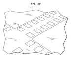
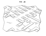
- FIGS. 2A , 2 B, 2 C, 2 D, 2 E, 2 F, 2 G, 2 H, and 21 are perspective view computer graphic images illustrating one process for forming microchips with interconnect nodules in accordance with one embodiment of the present invention
- FIG. 3 is a schematic illustration of a system-in-package architecture for mobile telephony using a quilt packaging system of the present invention
- FIG. 4 is a schematic diagram of a digital system using a quilt packing system in accordance with one embodiment of the present invention.
- FIG. 5 is a schematic diagram of a optical communication system using a quilt packing system in accordance with one embodiment of the present invention.
- FIG. 6 is a schematic diagram of a wafer with hexagonal microchips in accordance with one embodiment of the present invention.
- FIG. 7 is a schematic diagram of a wafer with square microchips in accordance with one embodiment of the present invention.
- FIG. 8 is a schematic diagram of a wafer with octagonal and square microchips in accordance with one embodiment of the present invention.
- FIG. 9 is a schematic diagram of octagonal microchips of FIG. 8 in a quilt packaging system of the present invention.
- FIG. 10A is a schematic partial top view of two microchips of the present invention including tabs and notches for aligning interconnect nodules on the two microchips with each other;
- FIG. 10B is a schematic partial top view of the two microchips of FIG. 10A , wherein the two microchips are aligned and the interconnect nodules of the two chips are in electrical communication with each other;
- FIG. 11A is a schematic cross-sectional partial side view of two microchips of the present invention being slid into engagement with each other;
- FIG. 11B is a schematic cross-sectional partial side view of the two microchips of FIG. 11A , wherein the two microchips are aligned and the interconnect nodules of the two chips are in electrical communication with each other;
- FIG. 11C is an enlarged cross-sectional partial side view of region C of FIG. 11B ;
- FIG. 11D is a schematic partial top view of the aligned microchips of FIGS. 11B and 11C ;
- FIG. 12A is a schematic cross-sectional partial side view of two microchips of the present invention being engaged with each other;
- FIG. 12B is a schematic cross-sectional partial side view of the two microchips of FIG. 12A , wherein the two microchips are aligned and the interconnect nodules of the two chips are in electrical communication with each other;
- FIG. 12C is an enlarged cross-sectional partial side view of region C′ of FIG. 12B ;
- FIG. 12D is a schematic partial top view of the aligned microchips of FIGS. 12B and 12C ;
- FIG. 13A is a schematic partial top view of two microchips having mating modulated edges in accordance with one embodiment of the present invention.
- FIG. 13B is a schematic partial top view of the two microchips of FIG. 13A electrically mated to each other and with their respective interconnect nodules in electrical communication with each other;
- FIG. 14 is a schematic partial top view of the microchips of FIG. 13A plugged into an electrical connector in accordance with one embodiment of the present invention
- FIG. 15 is a schematic partial top view of two microchips having protruding interconnect nodules plugged into an electrical connector in accordance with one embodiment of the present invention
- FIG. 16A is a schematic computer graphic view of a 3-dimensional quilt packaging system in accordance with one embodiment of the present invention having a rectangular shape;
- FIG. 16B is a schematic cross-sectional partial side view of an exemplary electrical connection between two microchips of the quilt packaging system of FIG. 16A ;
- FIG. 17A is a schematic computer graphic view of a 3-dimensional quilt packaging system in accordance with one embodiment of the present invention having a triangular shape
- FIG. 17B is a schematic cross-sectional partial side view of an exemplary electrical connection between two microchips of the quilt packaging system of FIG. 17A ;
- FIG. 18 is a schematic cross-sectional partial side view of a quilt packaging system having a branched configuration in accordance with one embodiment of the present invention.
- FIG. 19 is a schematic cross-sectional partial side view of a quilt packaging system having a branched configuration in accordance with one embodiment of the present invention.
- FIG. 20A is a schematic cross-sectional partial side view of a quilt packaging system including a microchip with lateral surface interconnect nodules in accordance with one embodiment of the present invention
- FIG. 20B is a schematic partial top view of the quilt packaging system of FIG. 20A ;
- FIG. 21A is a schematic cross-sectional partial side view of a quilt packaging system in which one microchip partially overlaps two other microchips to which the microchip is electrically connected in accordance with one embodiment of the present invention
- FIG. 21B is a schematic cross-sectional partial side view of the electrical connection between respective interconnect nodules of two of the microchips of FIG. 21A ;
- FIG. 21C is a schematic cross-sectional partial side view of the microchips of FIG. 21B before the microchips are electrically connected;
- FIG. 22A is a schematic partial top view of a semiconductor wafer in accordance with one embodiment of the present invention.
- FIG. 22B is a schematic cross-sectional partial side view of the semiconductor wafer of FIG. 22A ;
- FIG. 22C is a schematic partial top view of the semiconductor wafer of FIG. 22A into which trenches have been etched in accordance with one embodiment of the present invention
- FIG. 22D is a schematic cross-sectional partial side view of the semiconductor wafer of FIG. 22C ;
- FIG. 22E is a schematic partial top view of the semiconductor wafer of FIG. 22C having a conductive material deposited in the trenches in accordance with one embodiment of the present invention.
- FIG. 22F is a schematic cross-sectional partial side view of the semiconductor wafer of FIG. 22E ;
- FIG. 22G is a schematic partial top view of the wafer of FIG. 22E having circuitry deposited thereon;
- FIG. 22H is a schematic cross-sectional partial side view of the wafer of FIG. 22G ;
- FIG. 22I is a schematic partial top view of the semiconductor wafer of FIG. 22E being partially separated into two microchips in accordance with one embodiment of the present invention.
- FIG. 22J is a schematic cross-sectional partial side view of the two microchips of FIG. 22I ;
- FIG. 22K is a schematic partial top view of one of the two microchips of FIG. 22I ;
- FIG. 22L is a schematic cross-sectional partial side view of the microchips of FIG. 22K with a punch in the process of flattening conductive material of the microchip;
- FIG. 22M is a schematic partial top view of the semiconductor wafer of the microchip of FIG. 22K including protruding interconnect nodules;
- FIG. 22N is a schematic cross-sectional partial side view of the microchip of FIG. 22M and the punch flattening the conductive material of an interconnect nodule to make the interconnect nodule protrude;
- FIG. 23A is a schematic partial top view of two microchips and an intermediate electrical connector in accordance with one embodiment of the present invention.
- FIG. 23B is a schematic cross-sectional partial side view of the two microchips and intermediate electrical connector of FIG. 23A ;
- FIG. 23C is a schematic partial top view of the two microchips and intermediate electrical connector of FIG. 23A in which the two microchips are in electrical communication with the intermediate electrical connector;
- FIG. 23D is a schematic cross-sectional partial side view of the two microchips and intermediate electrical connector of FIG. 23C ;
- FIG. 24A is a schematic partial top view of the semiconductor wafer having a conductive material deposited in the trenches thereof and a circuitry deposited thereon in accordance with one embodiment of the present invention
- FIG. 24B is a schematic cross-sectional partial side view of the semiconductor wafer of FIG. 24A ;
- FIG. 24C is a schematic partial top view of the semiconductor wafer of FIG. 24A being mechanically etched by a rotating microsaw to form two partially-separated microchips;
- FIG. 24D is a schematic cross-sectional partial side view of the semiconductor wafer of FIG. 24A being mechanically etched by a rotating microsaw to form two partially-separated microchips;
- FIG. 24E is a schematic partial top view of additional conductive material being deposited on the interconnect nodules of the two microchips of FIGS. 24C and 24D to make the interconnect nodules protrude;
- FIG. 24F is a schematic cross-sectional partial side view of additional conductive material being deposited on the interconnect nodules of the two microchips of FIGS. 24C and 24D to make the interconnect nodules protrude;
- FIG. 24G is a schematic partial top view of the two microchips of FIGS. 24E and 24F after they have been fully separated by chemical or mechanical etching;
- FIG. 24H is a schematic cross-sectional partial side view of the two microchips of FIGS. 24E and 24F after they have been fully separated by chemical or mechanical etching;
- FIG. 25A is a schematic cross-sectional partial side view of microchips that are electrically connected to a PCB in accordance with one embodiment of the present invention.
- FIG. 25B is a schematic partial top view of the microchips and PCB of FIG. 25A ;
- FIG. 26A is a schematic cross-sectional partial side view of a microchip in the process of being placed in a special outlet in a PCB in accordance with one embodiment of the present invention
- FIG. 26B is a schematic cross-sectional partial side view of the microchip of FIG. 26A mounted in the PCB of FIG. 26A ;
- FIG. 26C is a schematic partial top view of the microchip and PCB of FIG. 26B ;
- FIG. 27A is a schematic partial top view of a quilt packaging system in accordance with one embodiment of the present invention that is electrically connected to a PCB by wire bonds;
- FIG. 27B is a schematic cross-sectional partial side view of the quilt packaging system and PCB of FIG. 27A ;
- FIG. 28A is a schematic partial top view of a quilt packaging system in accordance with one embodiment of the present invention that is electrically connected to a PCB by wire bonds;
- FIG. 28B is a schematic cross-sectional partial side view of the quilt packaging system and PCB of FIG. 28A ;
- FIG. 29A is a schematic partial top view of two microchips of the present invention having interconnect nodules with spheroid-shaped ends;
- FIG. 29B is a schematic partial cross-sectional side view of the two microchips of FIG. 29A ;
- FIG. 29C is a schematic partial top view of two microchips FIG. 29A being bonded together;
- FIG. 29D is a schematic partial cross-sectional side view of the two microchips of FIG. 29C ;
- FIG. 30A is a schematic partial top view of two microchips of the present invention wherein the interconnect nodules on one microchip have a blunt shape and the interconnect nodules on the other microchip having a sharp shape;
- FIG. 30B is a schematic partial cross-sectional side view of the two microchips of FIG. 30A ;
- FIG. 30C is a schematic partial top view of the two microchips of FIG. 30A being bonded together;
- FIG. 30D is a schematic partial cross-sectional side view of the two microchips of FIG. 30C ;
- FIG. 31A is a schematic partial cross-sectional side view of the two microchips in accordance with one embodiment of the present invention.
- FIG. 31B is a schematic partial cross-sectional side view of the microchips of FIG. 31A being bonded together using a laser beam;
- FIG. 32 is a schematic partial top view of two microchips of the present invention bonded together;
- FIG. 33A is a schematic partial top view of two microchips connected by a rigid connector in accordance with one embodiment of the present invention.
- FIG. 33B is a schematic partial cross-sectional side view of the two microchips and the connector of FIG. 33A ;
- FIG. 34A is a schematic partial top view of two microchips connected by a flexible connector in accordance with one embodiment of the present invention.
- FIG. 34B is a schematic partial cross-sectional side view of the two microchips and the connector of FIG. 34A ;
- FIG. 35A is a schematic partial top view of a dynamic sliding on-off quilt packaging system in an off-position in accordance with one embodiment of the present invention.
- FIG. 35B is a schematic partial top view of the dynamic sliding on-off quilt packaging system of FIG. 35A in an on-position;
- FIG. 36A is a schematic partial cross-sectional side view of a dynamic flexible on-off quilt packaging system in an off-position in accordance with one embodiment of the present invention
- FIG. 36B is a schematic partial cross-sectional side view of the dynamic flexible on-off quilt packaging system of FIG. 36A in an on-position;
- FIG. 37A is a micrograph of part of a microchip in accordance with one embodiment of the present invention.
- FIG. 37B is micrograph at greater magnification than the micrograph of FIG. 37A showing an interconnect nodule of the microchip of FIG. 37A ;
- FIG. 37C is a micrograph of part of a microchip in accordance with one embodiment of the present invention.
- FIG. 37D is micrograph at greater magnification than the micrograph of FIG. 37C showing an interconnect nodule of the microchip of FIG. 37C .
- convex refers to a microchip having the shape of a convex closed curve.
- convex shapes are: circles, triangles, squares, rectangles, parallelograms, rhombi, hexagons, octagons, etc.
- die-on-wafer refers to an integrated circuit that has been formed on a silicon wafer and is not yet separated from the wafer.
- direct electrical connection refers to the direct contact between interconnect nodules or between an interconnect nodule and an electrical contact so that electrical conduction current may pass between them.
- the term “electronic device” refers to electronic circuitry and any device that includes electronic circuitry.
- electronic devices include microchips, package systems, transistors, PCBs, amplifiers, sensors, inductors, capacitors, electrical connectors into which microchips may be plugged, etc.
- the term “interposer” refers to any structure whose purpose is to extend or complete a conductive electrical connection between two electronic devices.
- the conductive electrical connection between interconnect nodules or between an interconnect nodule and a contact may not be direct.
- a conductive material such as solder, may electrically connect two interconnect nodules or an interconnect nodule with an electrical contact.
- connectors of various types may help conductively electrically connect interconnect nodules.
- microchip refers to any kind of chip having microfabricated or nanofabricated systems built thereon. Microchips include not only conventional integrated circuits, but also, MEMS (Microelectromechanical Systems) chips.
- MEMS Microelectromechanical Systems
- non-convex refers to a microchip having the shape of a non-convex closed curve.
- single chip device refers to any device that has been made as a single chip.
- the quilt packaging system of the present invention allows for a single chip device to be made as a multi-chip quilt packaging system device.
- single chip devices include but are not limited to the following: CPUs, microprocessors, graphics processors, memory chips, MEMS, etc.
- SiP Advanced system-in-package
- Future systems will require combinations of radio frequency (RF), optoelectronics, high-speed logic, memory, and MEMS-enabled functionality, all combined into a single, compact, lightweight and low-power SiP.
- RF radio frequency
- a fundamental consideration in implementing a SiP design of this sort is how to accomplish heterogeneous integration of the various system components, without incurring unacceptable penalties in terms of either performance or cost.
- the ability to integrate circuits and components fabricated using disparate and incompatible fabrication processes (e.g. CMOS and bipolar) and materials (Si, III-V semiconductors) is critical for providing the means to realize, in a single package, higher levels of functionality than are presently possible.
- the quilt packaging system of the present invention uses the vertical facets on edges of a microchip to make direct electrical contact between integrated circuits. Metal or otherwise conductive nodules are revealed on the vertical surfaces of each microchip, and multiple microchips are welded together in a pattern reminiscent of a quilt to form high-performance electrical connections between the microchips. In this way, the delays and other constraints due to chip-to-package and package-to-chip data transfers are avoided.
- the quilt packaging system of the present invention allows for chips to be directly interconnected without the need to go through first-level packaging to printed circuit boards (PCBs) or multichip modules (MCMs).
- the quilt packaging system of the present invention forms contacts along the vertical edge facets of integrated circuits, enabling ICs or other types of microchips to be interconnected by placing them side-by-side.
- This technology may have a dramatic impact on the way portable and high-performance electronic systems are designed, particularly for complex or cost-sensitive applications. Possible applications include optical spectroscopy for on-chip chemical analysis, high-speed optical networking, RF communication systems, and advanced mixed-signal electronics.
- one process that may be used involves using deep reactive ion etching (DRIE) and metal plating, which together may be used to form solid metallic contacts along the vertical edge facets of one or more microchips.
- DRIE deep reactive ion etching
- metal plating which together may be used to form solid metallic contacts along the vertical edge facets of one or more microchips.
- the planar geometry of the edge interconnects promises ultra-high signal bandwidths and excellent signal integrity characteristics, while simultaneously achieving high pitch density.
- the quilt packaging system of the present invention provides an ultrafast, high density, inexpensive SiP packaging that embraces heterogeneous device technologies. Its potential impact can hardly be overstated.
- ITRS International Technology Roadmap for Semiconductors
- the quilt packaging system of the present invention provides a new concept in high-speed, high-density, heterogeneous integration. Also, RF systems using quilt packaging provide benefits in cost and performance as compared to current ways of mounting microchips. In addition, as described below and shown in the drawings, the present invention provides a process scheme for achieving chip features suitable for quilt packaging.
- the present invention also provides the ability to integrate circuits and components fabricated using disparate and incompatible fabrication processes and materials and offers the opportunity to realize, in a single package, higher levels of functionality than are presently possible.
- This approach provides solutions to realizing compact systems for advanced remote sensing, bio-chemical agent detection, electronic communications, and high-performance networking applications where heterogeneous integration of sensors, optoelectronic devices, and high-performance electronics are required.
- the present invention provides a technique for interconnecting directly between adjacent chips without the need to go through first-level packaging to PCBs or MCMs.
- This approach facilitates integration of, within a single package, silicon and III-V, II-VI or IV-IV semiconductor ICs while simultaneously improving the bandwidth and signal integrity of the interconnections between these devices and circuits.
- the packaging approach of the present invention is a natural means to achieve true SiP and system-on-chip (SoC) implementations.
- the quilt packaging system of the present invention has applications in a number of advanced RF and communications applications requiring either high electrical interconnect performance or the integration of optoelectronic, electronic, and sensory components in a single package.
- Applications include ultracompact RF communications equipment, high-speed optical networking, advanced mixed-signal electronics, as well as bio-chemical agent detection and remote sensing.
- the quilt packaging system of the present invention may provide: enhanced heat dissipation through support chips, system cost reduction by allowing increased functionality within a single package, heterogeneous integration of ICs and components fabricated using different processes (e.g. bipolar and CMOS) and material systems (e.g. Si and III-V semiconductors), functional partitioning of ICs allowing complex designs to be broken into functional sub-block ICs and integrated into a full system in a single package, increased usable wafer area and silicon efficiency by elimination of saw streets and bond pads, decreased weight and volume of chip and board structures, circuit simplification and area reduction through elimination of ESD protection circuits and high-power pin drivers.
- CMOS complementary metal-oxide
- material systems e.g. Si and III-V semiconductors
- functional partitioning of ICs allowing complex designs to be broken into functional sub-block ICs and integrated into a full system in a single package
- increased usable wafer area and silicon efficiency by elimination of saw streets and bond pads
- the microchips and other electrical components in the quilt packaging system are conductively connected over much reduced distances compared with conventional interconnect technologies, for example PCBs, the capacitance of the interconnects that run between the electrical systems is significantly reduced, and the pad drivers and their associated power dissipation can be eliminated. Significant reductions in overall circuit power dissipation result.
- the quilt packaging system may be used by itself or in combination with existing bonding techniques for microchips and electronic devices.
- the quilt packaging system of the present invention employs DRIE and plating to form metal-filled deep trenches at the edges of a die-on-wafer to provide an additional means of interconnection besides bonding pads/wires.
- the various die-on-wafer in the system are interconnected either wholly or partly by butting them edgewise against each other, as depicted in the embodiment of the present invention shown in FIG. 1 .
- Conventional wirebonds may still be used to provide interconnections to next-level packaging and conventional pin arrays and lead frames.
- FIG. 1 is a simplified representation of two IC chips 102 and 104 of the present invention including edge interconnections. For clarity, the scales have been exaggerated in FIG. 1 .
- Notches 112 and 114 at respective front edges of chips 102 and 104 are cutaways to show the details of respective interconnect regions 122 and 124 .
- Chips 102 and 104 also include several layers of circuitry 126 and 128 that include terminal ends 130 and 132 at interconnect regions 122 and 124 .
- FIG. 1 Although for simplicity, there are only 4 interconnect regions shown for each chip in FIG. 1 , in actual chips there may be many more than 4 interconnect regions. Also, although in FIG. 1 it appears that only one layer of circuitry has terminal ends in the interconnect regions, the chips of the present invention may have terminal ends in more than one circuitry layer of the chip. In FIG. 1 and in all of the drawings described below, unless otherwise specified, there are several layers of circuitry in each of the IC chips that is represented by one or two layers of “simplified circuitry” for convenience of illustration.
- the protruding edge interconnection nodules may be formed by DRIE of trenches and grooves, followed by plating to fill the grooves and form the nodules.
- the trenches will be designed for easy die separation leaving metallized nodules on the edges of the wafer. Assuming a die edge of 10 mm and a nodule pitch of 20 ⁇ m, two thousand such nodules could be fabricated along the periphery. Larger chips and finer pitch may allow yet more nodules to be disposed along the periphery. Nodules may be plated up to extend beyond the edge of the die-on-wafer so that physical contact between adjacent die on any conventional package support substrate may be achieved.
- FIGS. 2A , 2 B, 2 C, 2 D, 2 E, 2 F, 2 G, 2 H and 2 I illustrate a process for forming microchips of the present invention.
- the various features shown in FIGS. 2A , 2 B, 2 C, 2 D, 2 E, 2 F, 2 G, 2 H and 2 I are not drawn to scale and many features have been enlarged to better show detail.
- FIG. 2A a semiconductor wafer 202 is shown including microchips 204 each of which is separated from a neighboring microchip 204 by spacer regions 206 .
- Trenches 210 are etched in spacer regions 206 alongside edges 212 of each microchip 204 as shown in FIG. 2B .
- trenches 210 in one spacer region 206 in greater detail.
- the exposed surfaces of trenches 210 are passivated by forming an oxide layer 216 on the exposed surfaces of trenches 210 by using a known semiconductor oxidation technique.
- the passivation of trenches 210 electrically isolates the metal interconnect nodules (described below) that are deposited in the holes from the rest of semiconductor wafer 202 .
- a resist coating is applied to wafer 202 . After the resist coating is applied, the resist coating is removed from trenches 210 to form openings. Then, metal is deposited into trenches 210 through the openings in the resist. Next the resist is removed.
- FIG. 2E An electroless plating process is then applied to the deposited seed metal to form metal interconnect nodules 224 , as shown in FIG. 2E . Then metal interconnect nodules 224 are subject to chemical mechanical polishing (CMP). The appearance of metal interconnect nodules 224 after polishing is shown in FIG. 2F . Intermetal dielectric material is then deposited prior to forming electrical connections 232 with on-chip wiring (not shown) as shown in FIG. 2G . After electrical connections 232 are formed, microchips 204 that include interconnect nodules 224 and spacer regions 244 are separated from each other using DRIE. FIG. 2H shows wafer 202 as wafer 202 appears after DRIE with portions 246 still connecting microchips 204 . FIG.
- FIG. 2H also shows how spacer regions 244 may be further etched between interconnect nodules 224 so that interconnect nodules 224 protrude laterally from chips 204 .
- Final separation of microchips 204 from each other may be completed by backside wafer thinning. Separated microchips 204 are shown in FIG. 2I .
- the semiconductor wafer of FIGS. 2A , 2 B, 2 C, 2 D, 2 E, 2 F, 2 G, and 2 H may be made of any type of semiconductor material such as Si, GaAs, etc.
- the surfaces of the trenches 210 are passivated using PECVD nitride.
- Other methods of passivating the surfaces of the trenches include PECVD oxide, sputtered oxide, low-k dielectrics, or other dielectric materials.
- a seed may then be applied to trenches prior to depositing metal in the trenches to ensure that the deposited metal will end up in the trenches and not elsewhere on the silicon wafer.
- Suitable seed materials for the purposes of the present invention are well known to those in the art.
- the holes in the semiconductor wafer used to mold the interconnect nodules are formed by photolithography and DRIE.
- Other methods of forming the trenches of the present invention include such lithographic techniques as electron beam, x-ray, extreme ultraviolet and any other method that may be used to form patterns on a semiconductor substrate.
- the trenches may be formed by RIE, isotropic wet etching and other suitable etching techniques.
- Chemical mechanical polishing (CMP) techniques that may be used in polishing metal interconnect nodules of the present invention include suitable planarization methods used with semiconductor wafers.
- the interconnect nodule metallization plating may be copper, gold, or other malleable low-resistance material with an overlay of a flowable solder material, although pure metals such as copper or gold alone may be used with an ultrasonic weld step.
- Exposure of the interconnect nodules to form protruding interconnect nodules may be accomplished by performing first an anisotropic etch for depth below the nodules, with substrate material remaining directly beneath the nodules, followed by an isotropic etch that causes the vertical surfaces of the die to recede, allowing the nodules to protrude beyond the edges of the die.
- Large interconnect nodules and large pitches may be exposed by using isotropic etching or crystallographic etching, whereas small nodules and fine pitch may require both anisotropic and isotropic etch techniques combined.
- the interconnect nodules of two microchips of the present invention may be placed in electrical communication with each other by thermomechanical or ultrasonic bonding, heat welding, laser welding, etc. Other particular techniques for electrically connecting the interconnect nodules of the present invention are described below.
- FIG. 3 shows one system-in-package architecture 300 for mobile telephony using a quilt packaging system in accordance with one embodiment of the present invention.
- a baseband processor microchip 302 with CMOS is directly electrically connected to a III-V based power amplifier microchip 304 by interconnect nodules 306 and 308 of microchip 302 and microchip 304 , respectively.
- Microchip 302 is directly electrically connected to an RF signal processing block microchip 312 with SiGe HBTs (Heterostructure Bipolar Transistors) by interconnect nodules 316 and 318 of microchip 302 and microchip 312 , respectively.
- SiGe HBTs Heterostructure Bipolar Transistors
- Microchip 302 is connected to an NMOS-based audio amplifier and voltage regulator sub-block microchip 322 by interconnect nodules 326 and 328 of microchip 302 and microchip 322 , respectively.
- Microchip 304 is directly electrically connected to microchip 312 by interconnect nodules 336 and 338 of microchip 304 and microchip 312 , respectively.
- Microchip 312 is directly electrically connected to microchip 322 by interconnect nodules 346 and 348 of microchip 312 and microchip 322 , respectively.
- FIG. 4 shows a system-in-package architecture 400 for one digital processing system using a quilt packaging system in accordance with one embodiment of the present invention.
- a CPU 402 is directly electrically connected to an I/O microchip 404 by interconnect nodules 406 and 408 of microchip 402 and microchip 404 , respectively.
- Microchip 402 is directly electrically connected to Video IC microchip 412 by interconnect nodules 416 and 418 of microchip 402 and microchip 412 , respectively.
- Microchip 402 is connected to dual-port memory microchip 422 by interconnect nodules 426 and 428 of microchip 402 and 422 , respectively.
- Microchip 404 is directly electrically connected to microchip 412 by interconnect nodules 436 and 438 of microchip 404 and microchip 412 , respectively.
- Microchip 412 is directly electrically connected to microchip 422 by interconnect nodules 446 and 448 of microchip 412 and microchip 422 , respectively.
- the quilt packaging system of the present invention may provide cooling of hot components in a quilt package system by allowing for heat transfer between hotter and cooler components.
- heat from microchip 402 may flow to microchips 404 and 422 as indicated by arrows 450 and 452 due to direct thermal contact between microchip 402 and microchips 404 and 422 .
- FIG. 5 shows a system-in-package architecture 500 for optical communication system using a quilt packaging system in accordance with one embodiment of the present invention.
- a CPU 502 is directly electrically connected to a III-V PD (Photo Diode) Array microchip 504 by interconnect nodules 506 and 508 of microchip 502 and microchip 504 , respectively.
- Microchip 502 is directly electrically connected to a III-V laser array microchip 512 by interconnect nodules 516 and 518 of microchip 502 and microchip 512 , respectively.
- Microchip 504 is connected to Si optical bench microchip 522 by interconnect nodules 526 and 528 of microchip 504 and 522 , respectively.
- Microchip 512 is directly electrically connected to a Si optical bench microchip 532 by interconnect nodules 536 and 538 of microchip 512 and microchip 532 , respectively.
- Microchip 522 includes a coupling lens array 542 and microchip 532 includes a coupling lens array 544 .
- Incoming optical signals 552 enter microchip 522 by optical fibers 554 extending into microchip 522 and outbound optical signals 556 exit microchip 532 by optical fibers 558 extending from microchip 532 .
- the pitch of the interconnect nodules in FIGS. 3 and 4 is shown as being 10 ⁇ m, but other pitches may be used as well depending on the size of the chips and interconnect nodules used.
- ICs or other electronic devices that are fabricated with dramatically different processes may be integrated together in a single package, raising the possibility of integration with III-V and other devices (e.g. III-V power amplifiers, SiGe low-noise amplifiers, etc.) for RF communications, as well as the functional integration of silicon-based circuits utilizing incompatible fabrication processes.
- III-V and other devices e.g. III-V power amplifiers, SiGe low-noise amplifiers, etc.
- any system requiring compact integration of devices, sensors, and integrated circuits can be interconnected using this technique, and reap the benefits of compact implementation and high-performance electrical interconnections.
- the quilt packaging approach does not preclude the simultaneous use of other dense packaging approaches, including conventional wire bonding, flip chip, and ball grid array techniques. Edge interconnection using interconnect nodules is complementary and can be used to augment these preexisting approaches.
- the present invention provides a novel solution to the problem of continued proliferation of interconnect pads following Rent's rule (P. Christie and D. Stroobandt, “The Interpretation and Application of Rent's Rule,” IEEE Trans. on VLSI Systems, Special Issue on System - Level Interconnect Prediction , vol. 8, no. 6, pp. 639-648, 2000) and the increase in number of logic gates per die-on-wafer as predicted by the ITRS.
- Rent's rule P. Christie and D. Stroobandt, “The Interpretation and Application of Rent's Rule,” IEEE Trans. on VLSI Systems, Special Issue on System - Level Interconnect Prediction , vol. 8, no. 6, pp. 639-648, 2000
- Irvine Sensors Corporation Costa Mesa, Calif. has made attempts to solve the problem of the proliferation of interconnect pads using stacked memory die techniques. This technique makes use of a 3D packaging concept, but requires chips to be thinned, stacked, and interconnected both through the wafers and along the edges of the stacks.
- the quilt packaging system of the present invention provides at least three advantages compared to the Irvine Sensors techniques.
- the quilt packaging system of the present invention provides better thermal control, since each die is heat-sinked directly to a package substrate.
- the quilt packaging system of the present invention provides higher speed, since each microchip may be contiguous with one or more other die, and possibly more if several smaller die are adjacent to a large one, for example as shown in the baseband processor of FIG. 4 .
- Another advantage of the quilt packing technique of the present invention is that the system may be used to achieve wide-bandwidths while remaining resonance-free, by avoiding the electromagnetic discontinuity arising from the radical changes in transmission line properties for horizontal to vertical interconnects. Such issues will become critical as signal frequencies extend well into the multi-GHz regime.
- the quilt packaging system of the present invention may provide ultrawide interconnect bandwidths and excellent signal integrity. Many benefits and opportunities resulting from the quilt packaging system are discussed below.
- the quilt packaging system of the present invention provides high-speed, high-signal-integrity chip-to-chip interconnects.
- the quilt packaging system of the present invention may also provide high-speed, low-loss, and low-noise characteristics for critical applications within SiPs.
- a high-speed interface with good signal integrity performance may be provided by the quilt packaging system of the present invention due to the edge interconnect geometry.
- the quilt interconnect geometry essentially results in an extension, from one chip to the next, of the same planar interconnect geometry as is used within a chip. As a consequence of this preservation of the conventional on-chip interconnect geometry, the electromagnetic discontinuities that are inherent in wirebond-based interconnects (and to a lesser degree in flip-chip implementations) may be eliminated almost entirely.
- each piece of the SiP may be fabricated most efficiently using the best technology for its specific function without compromising either cost or performance due to manufacturing multiple technologies on a single substrate. As shown in FIGS.
- the major components of a mobile telephony handset, digital system, optical communications system, or other advanced system using heterogeneous IC technologies may be integrated in a single package through quilt packaging.
- This integration results in a unique combination of exceptional power and energy efficiency, cost efficiency, flexibility in fabrication and individual function optimization (e.g. SiGe RF processor/LNA, III-V power amplifier, CMOS baseband processor), and high interconnect performance.
- Such heterogeneous integration across disparate material systems and fabrication processes permits straightforward and cost-effective SiP implementations.
- the quilt packaging system of the present invention also provides a low cost packaging system for microchips, even with increased system performance.
- the quilt packaging system of the present invention may allow the combining of multiple die into a single package with increased speed and lower noise, as well as with greatly increased design flexibility since each microchip may be fabricated using different technologies and/or material systems.
- the need for fewer packages, which add significantly to the final microchip cost, may lower the system cost considerably.
- Conventional wafer-level packaging (WLP) and chip-scale packaging (CSP) technologies are often regarded as best suited for economical but lower-performance packaging needs.
- the quilt packaging system of the present invention may be used to extend WLP's reach into higher performance applications as well.
- the quilt packaging system of the present invention offers high chip real estate efficiency.
- support circuitry such as pad drivers and electrostatic discharge (ESD) protection may be obviated for many signal lines since ICs will interface directly to each other within a single package rather than to long wires (wire bonds and PCB traces) with connections to the outside world and thus subject to ESD. This will result in even greater savings in chip real estate, enhanced reliability from the standpoints of both improved system ESD immunity and that of manufacturing (omission of ESD circuitry), and enhanced energy efficiency.
- the quilt packing system of the present invention provides lower kerf losses than current packaging systems. Manufacturing costs for quilt packaging systems are lower than for current packaging systems due to the “free” streets for die-on-wafer separation without the need for wafer sawing.
- the ITRS indicates that die sizes will saturate and may even shrink toward the year 2016. In this case, it is unlikely that wafer dicing saw technology will keep pace, so a continually larger fraction of the wafer area will be dedicated to kerf and sawing issues.
- the improved areal efficiency may result in additional die per wafer. For example, in today's 200 mm wafer technology, elimination of the streets would result in about 4 additional 10 ⁇ 10 mm die per wafer. This savings would of course increase further for die on 300 mm wafers.
- the present invention provides a non-rectangular microchip.
- FIG. 6 shows a wafer 602 having 19 hexagonal microchips 604 formed thereon and having wasted space 606 .
- FIG. 7 shows a wafer 702 having 17 square microchips 704 formed thereon and having wasted space 706 .
- more hexagonal chips may be formed from a given wafer and there is less wastage.
- forming hexagonal chips rather than rectangular may result in an increase in wafer space utilization that provides significant economic value.
- the present invention provides octagonal microchips.
- FIG. 8 illustrates how a wafer 802 may have octagonal microchips 804 formed thereon. In between octagonal microchips 804 are square microchips 806 . Surrounding microchips 804 and microchips 806 is wasted space 808 .
- octagonal and square microchips are shown being formed on the same wafer in FIG. 9 , in some embodiments of the present invention, it may be desirable to form only octagonal chips on a given wafer.
- FIG. 9 shows how octagonal microchips 904 may be arranged in a quilt packaging system 922 of the present invention. Between one set of two microchips 904 is an interposer 924 that provides a bi-directional electrical connection. Between two microchips 904 is an interposer 926 that provides a quadra-directional electrical connection between four microchips 904 . Instead of interposers 924 or 926 , other square microchips 932 could be placed.
- connections are shown between the octagonal microchips in FIG. 9 , in other embodiments of the present invention, there may simply be openings between the octagonal microchips to allow for cooling and other purposes.
- microchips all having the same shape or having different shapes may be formed on the same wafer.
- the microchips of the present invention may have various types of convex shape such as triangular, rectangular, circular, rhomboid, etc. and may or may not be bilaterally or rotationally symmetric.
- the microchips of the present invention may even have simple or complex non-convex shapes.
- the microchips of the present invention include alignment means for aligning of wafers during assembly, which provides increased speed and reliability during manufacturing.
- the microchips of the present invention also provide for non-conventional ways of obtaining electrical connections on microchip edges.
- the microchips of the present invention allow for increasing the flexibility of wafer connections and speeds the manufacturing process.
- the microchips of the present invention may be connected with PCBs or other devices.
- the microchips of the present invention may be direct-conductively connected to PCBs.
- the microchips may have complex shapes and include means for aligning the interconnect nodules with each other or with other devices such as PCBs or other chips to which the microchips of the present invention are electrically connected, as illustrated, for example, in FIGS. 10A and 10B .
- Such aligning means may take the form of tabs, pins, etc. and may be unitary with the rest of the microchip or may be embedded or attached to the microchips during manufacturing.
- FIG. 10A shows two microchips 1002 and 1004 of the present invention and FIG. 10B shows microchips 1002 and 1004 in electrical communication.
- Microchip 1002 has an integral alignment tab 1012 and an alignment notch 1014 on an edge 1016 of microchip 1002 .
- Microchip 1004 has an integral alignment notch 1022 and an alignment tab 1024 on an edge 1026 of microchip 1004 . As shown in FIG. 10B , alignment tab 1012 fits into alignment notch 1022 and alignment tab 1024 fits into alignment notch 1014 to align respective interconnect nodules 1032 and 1034 of microchips 1002 and 1004 when interconnect nodules 1032 and 1034 make contact with each other.
- the means for aligning two electrically connected microchips of the present invention may restrict the motion of the two connected microchips along the axis that the microchips are in electrical communication.
- FIG. 11A shows microchips 1102 and 1104 being slid along an axis of motion 1106 into engagement with each other.
- FIGS. 11B , 11 C and 11 D show microchips 1102 and 1104 in electrical communication with each other.
- Microchip 1102 has an integral trapezoidal alignment tab 1112 on an edge 1116 of microchip 1102 .
- Microchip 1104 has a trapezoidal alignment notch 1124 on an edge 1126 of microchip 1104 . As shown in FIG.
- alignment tab 1112 fits into alignment notch 1124 to align respective interconnect nodules 1132 and 1134 of microchips 1102 and 1104 when interconnect nodules 1132 and 1134 make contact with each other. Also, the shapes of alignment tab 1112 and alignment notch 1124 restrict the motion of microchips 1102 and 1104 along axis 1142 of electrical communication between interconnect nodules 1132 and 1134 .
- FIGS. 12A , 12 B, 12 C, and 12 D show another embodiment of the present invention that includes a means for aligning two electrically connected microchips and restricting the motion of the two connected microchips along the axis that the microchips are in electrical communication.
- FIG. 12A shows microchips 1202 and 1204 being rotated together in the direction shown by arrows 1206 into engagement with each other.
- FIGS. 12B , 12 C and 12 D show microchips 1202 and 1204 in electrical communication with each other.
- Microchip 1202 has an integral trapezoidal alignment tab 1212 on an edge 1216 of microchip 1202 .
- Microchip 1204 has a trapezoidal alignment notch 1224 on an edge 1226 of microchip 1204 . As shown in FIG.
- alignment tab 1212 fits into alignment notch 1224 to align respective interconnect nodules 1232 and 1234 of microchips 1202 and 1204 when interconnect nodules 1232 and 1234 make contact with each other. Also, the shapes of alignment tab 1212 and alignment notch 1224 dovetail with each other and restrict the motion of microchips 1202 and 1204 along axis 1242 of electrical communication between interconnect nodules 1232 and 1234 .
- FIGS. 13A and 13B show two microchips 1302 and 1304 having respective modulated edges 1306 and 1308 .
- Modulated edge 1306 includes tabs 1312 and notches 1314 in which there are mounted tab interconnect nodules 1316 and notch interconnect nodules 1318 .
- Modulated edge 1308 includes tabs 1322 and notches 1324 in which there are mounted tab interconnect nodules 1326 and notch interconnect nodules 1328 . As shown in FIG.
- tabs 1312 and notches 1324 align and interconnect nodules 1316 and interconnect nodules 1328 and notches 1314 and tabs 1322 align interconnect nodules 1318 with interconnect nodules 1326 .
- the tabs and notches of the microchips of FIGS. 13A and 13B may have other shapes, such as the trapezoidal shape shown in the microchips of FIGS. 11A-D and 12 A-D to allow the tabs and notches to dovetail and restrict the motion of the microchips along the axis of electrical communication between the respective interconnect nodules.
- FIGS. 10A , 10 B, 11 A, 11 B, 11 C, 11 D, 12 A, 12 B, 12 C, 12 D, 13 A, and 13 B show two microchips are shown being aligned with respect to each other, the present invention also envisions similar types of alignment means to align the interconnect nodules of a microchip with the electrical contacts of an electronic device that are in electrical communication with the interconnect nodules of the microchip.
- the internal circuitry of the microchips in FIGS. 10A , 10 B, 11 A, 11 B, 11 C, 11 D, 12 A, 12 B, 12 C, 12 D, 13 A, and 13 B has been not shown for the purposes of simplicity.
- FIG. 14 shows microchips 1302 and 1304 plugged into an electrical connector 1402 having modulated edges 1404 and 1406 .
- Modulated edge 1404 includes notches 1412 and tabs 1414 in which there are mounted notch contacts 1416 and tab contacts 1418 .
- Modulated edge 1406 includes notches 1422 and tabs 1424 in which there are mounted notch contacts 1426 and tab contacts 1428 .
- Tab interconnect nodules 1316 electrically contact notch contacts 1416 and notch interconnect nodules 1318 contact tab contacts 1418 .
- Tab interconnect nodules 1326 electrically contact notch contacts 1426 and notch interconnect nodules 1328 contact tab contacts 1428 .
- the internal circuitry of microchips 1302 and 1304 and of connector 1402 are not shown for simplicity.
- FIG. 15 shows how microchips 1502 and 1504 that have protruding interconnect nodules 1506 and 1508 respectively may be plugged into an electrical connector 1512 that includes electrical contacts 1516 and 1518 .
- Interconnect nodules 1506 make electrical contact with contacts 1516 and interconnect nodules 1508 make electrical contact with contacts 1518 .
- the internal circuitry of microchips 1502 and 1504 and of connector 1512 are not shown for simplicity.
- FIGS. 14 and 15 are meant to only be exemplary of the ways that a microchip of the present invention may be plugged into another electronic device.
- the type of connectors that may be used with the microchips of the present invention are not limited to the embodiments shown in FIGS. 14 and 15 .
- a connector may have a series of places where microchips may be plugged into the connector, a connector may not only have places on one side of the connector where microchips may be plugged in, the connector may be part of a larger electronic device such as an amplifier, CPU, etc.
- FIG. 16A shows a 3-dimensional quilt package system 1602 of the present invention in which microchips 1612 , 1614 , 1616 and 1618 of the present invention are connected in a rectangular configuration.
- FIG. 16B shows how interconnect nodules 1622 and 1624 of microchips 1612 and 1614 are electrically connected to each other at a right angle.
- FIG. 17A shows a 3-dimensional quilt packaging system 1702 of the present invention in which microchips 1712 , 1714 and 1716 of the present invention are electrically connected in a triangular configuration.
- FIG. 17B shows how interconnect nodules 1722 and 1724 of microchips 1712 and 1714 are electrically connected to each other at an acute angle.
- FIGS. 16B and 17B Although one exemplary electrical connection of two microchips is shown in FIGS. 16B and 17B , similar connections are made between the interconnect contacts of the microchips along the other edges of each microchip where the microchips meet. Also, although two 3-dimensional shapes for a quilt packaging system of the present invention are shown in FIGS. 16A and 17A , a 3-dimensional quilt packaging system of the present invention may have any of a variety of shapes depending on the application. Among the advantages of 3-dimensional quilt packaging systems is their ability to provide cooling due to air or fluid movement along the microchip surfaces and the placement of interconnect nodules internally.
- microchips 1802 and 1804 are electrically connected in a lateral direction to each other by interconnect nodules 1806 and 1808 of microchips 1802 and 1804 , respectively.
- Microchip 1802 is electrically connected to microchip 1812 at a right angle by interconnect nodule 1814 of microchip 1812 and interconnect nodule 1806 .
- Microchip 1804 is electrically connected to microchip 1822 at a right angle by interconnect nodule 1824 of microchip 1822 and interconnect nodule 1808 .
- microchips 1902 and 1904 are electrically connected to each other in the lateral direction by interconnect nodules 1906 and 1908 of microchips 1902 and 1904 , respectively.
- Microchip 1902 is electrically connected to microchip 1912 at an acute angle by interconnect nodule 1914 of microchip 1912 and interconnect nodule 1906 of microchip 1902 .
- Microchip 1904 is electrically connected to microchip 1922 at an acute angle by interconnect nodule 1924 of microchip 1922 and interconnect nodule 1908 of microchip 1904 .
- the interconnect nodules are described as being on the edges of a microchip, in other embodiments the interconnect nodules may be located on one or both lateral surfaces of a microchip or located on both the lateral surfaces and edges of a microchip. Such microchips may be formed following a procedure similar to that shown in FIGS. 2A-2I by depositing the interconnect nodules on one or both lateral surfaces of a die-on-wafer.
- FIGS. 20A and 2013 show a microchip 2002 of the present invention having lateral surface interconnect nodules 2004 on a lateral surface 2006 of microchip 2002 .
- Microchips 2012 have edge interconnect nodules 2014 that are electrically connected to respective interconnect nodules 2004 of microchip 2002 .
- Microchip 2002 also includes conventional electric leads shown in the figure as wirebonds 2022 .
- FIG. 20B shows the top view of the embodiment of FIG. 20A .
- the quilt packaging system may employ face-to-face overlapping electrical connections between interconnect nodules of different microchips.
- FIGS. 21A and 21B show a microchip 2102 that partially overlaps a microchip 2104 and a microchip 2106 .
- Interconnect nodule 2112 of microchip 2102 makes a face-to-face electrical connection with interconnect nodule 2114 of microchip 2104 .
- Interconnect nodule 2122 of microchip 2102 makes a face-to-face electrical connection with interconnect nodule 2124 of microchip 2106 .
- FIG. 21C shows microchips 2102 and 2104 before they are electrically connected.
- FIGS. 22A-22N show a semiconductor wafer 2202 .
- FIGS. 22C and 22D show trenches 2204 etched in the semiconductor wafer.
- FIGS. 22E and 22F show a conductive material 2212 deposited in trenches 2204 .
- FIGS. 22G and 22H show circuitry 2214 deposited on substrate 2202 .
- FIGS. 22A-22N show a semiconductor wafer 2202 .
- FIGS. 22C and 22D show trenches 2204 etched in the semiconductor wafer.
- FIGS. 22E and 22F show a conductive material 2212 deposited in trenches 2204 .
- FIGS. 22G and 22H show circuitry 2214 deposited on substrate 2202 .
- FIGS. 22K , 22 L, 22 M, and 22 N show the conductive material 2212 of interconnect nodules 2206 being flattened by a punch 2232 to form protruding interconnect nodules 2234 .
- an intermediate connector or interposer with contacts made from a malleable material may provide a conductive but non-direct contact between non-protruding interconnect nodules.
- FIGS. 23A , 23 B, 23 C, and 23 D show an intermediate connector 2302 used to electrically connect two microchips 2304 and 2306 .
- microchip 2304 includes circuitry 2312 and interconnect nodules 2314
- microchip 2306 includes circuitry 2322 and interconnect nodules 2324 .
- Intermediate connector 2302 includes contacts 2342 .
- FIGS. 23C and 23D when microchips 2304 and 2306 are pressed against intermediate connector 2302 , interconnect nodules 2314 and 2324 deform and make electrical contact with contacts 2342 .
- an interposer with non-deformable contacts may also be used to electrically connect the interconnect nodules of two or more microchips.
- a connector may include alignment means of the type described above with respect to two microchips directly with each other and/or various types of engagement means, similar to the dovetail tab and notch combinations described previously, that interact with engagement means on the edge of the microchips to keep the interconnect nodules of the microchips in electrical communication with the interposer.
- an additional conductive metal such as copper, gold, etc. is deposited on the interconnect nodules of a microchip.
- Such a process may include the conventional stages of microchip production along with pressing out of the metal surface, preliminary dicing using a grinding plate, diamond cutter, deep etching or other known method to create deep grooves in the wafer surface. Deposition of the conductive metal may be made using any applicable method. The microchips may then be separated into separate microchips. FIGS. 24A , 24 B, 24 C, 24 D, 24 E, 24 F, 24 G, and 24 H show one such process.
- FIGS. 24A and 24B show a semiconductor wafer 2402 having trenches (not visible) in which has been deposited a conductive material 2404 . Circuitry 2406 has also been deposited on semiconductor wafer 2402 .
- FIGS. 24C and 24D show the use of a rotating microsaw 2422 to partially separate semiconductor wafer 2402 into two microchips 2432 and 2434 having respective non-protruding interconnect nodules 2436 and 2438 respectively.
- FIGS. 24E and 24F show additional conductive material 2442 and 2444 deposited on interconnect nodules 2436 and 2438 to make interconnect nodules 2436 and 2438 protrude.
- FIGS. 24G and 24H show the results of chemical or mechanical etching to fully separate microchips 2432 and 2434 from each other.
- the quilt packaging system of the present invention may be used to provide electrical connections between microchips of the present inventions and PCBs. Utilizing edge contacts instead of, or in addition to conventional contacts may increase connection speed, reliability, etc.
- FIGS. 25A and 25B shows one way of implementing an embodiment in which microchips are electrically connected to a PCB.
- a series of microchips 2502 are electrically connected by interconnect nodules 2504 to electrically conductive contact bars 2506 mounted on a PCB 2508 .
- the interconnect nodules of FIGS. 25A and 25B may be held in contact with the contact bars in several ways.
- the PCB may include notches between the contact bars that engage tabs of the interconnect nodules.
- Other ways of holding the microchips in place on the PCB include ultrasonic welding, laser welding, thermomechanical bonding, solder, etc.
- microchips may be electrically connected to a PCB by installing each microchip in a special outlet created on the PCB that is equipped with appropriate contact areas.
- FIGS. 26A , 26 B and 26 C An example of such a configuration is shown in FIGS. 26A , 26 B and 26 C.
- FIG. 26A shows a microchip 2602 having interconnect nodules 2604 and a PCB 2612 having a recessed outlet 2614 including contacts 2616 that are electrically connected to contact bars 2618 .
- Contact bars 2618 may be used to mount additional microchips (not shown) as shown in FIGS. 26A and 26B .
- interconnect nodules in the production of conventional microchips connected to a PCB with wirebonds.
- the interconnect nodules may serve as outlets for testing or for additional functions, such as entering security codes that should not be entered through conventional contacts such as wirebonds.
- microchips with wirebonds to which microchips of the present invention may be connected as shown in FIGS. 27A , 27 B, 28 A and 28 B.
- FIGS. 27A and 27B show a quilt packaging system 2702 of the present invention including four square microchips 2704 and a rectangular microchip 2706 that are connected together by interconnect nodules (not shown). Quilt packaging system 2702 is electrically connected to contact bars 2712 of a PCB 2714 by wirebonds 2716 extending from rectangular microchip 2706 .
- FIGS. 28A and 28B show a quilt packaging system 2802 of the present invention including four peripheral hexagonal microchips 2804 and a central hexagonal microchip 2806 that are connected together by interconnect nodules (not shown). Quilt packaging system 2802 is electrically connected to contact bars 2812 of a PCB 2814 by wirebonds 2816 extending from central hexagonal microchip 2806 .
- microchips Although only a few shapes of microchips are shown being interconnected in the quilt packaging systems of FIGS. 27A , 27 B, 28 A and 28 B, various combinations of microchip shapes may be used in a quilt packaging system that is wirebonded to a PCB.
- an octagonal microchip that is wire bonded to a PCB may be connected by interconnect nodules to square chips and/or rectangular microchips and/or hexagonal microchips.
- FIGS. 29A and 29B show two microchips 2902 and 2904 having spheroid-shaped end interconnect nodules 2912 and spheroid-shaped end interconnect nodules 2914 , respectively, connected to circuitry 2916 and 2918 , respectively.
- FIGS. 29A and 29B show two microchips 2902 and 2904 having spheroid-shaped end interconnect nodules 2912 and spheroid-shaped end interconnect nodules 2914 , respectively, connected to circuitry 2916 and 2918 , respectively.
- 29C and 29D show microchips 2902 and 2904 pushed against each other to deform interconnect nodules 2912 and interconnect nodules 2914 as interconnect nodules 2912 and interconnect nodules 2914 are driven into each other, indicated by arrows 2932 and 2934 and as ultrasonic welding is applied, indicated by sinusoids 2936 and 2938 , to bond together interconnect nodules 2912 and 2914 .
- FIGS. 29C and 29D are ultrasonic welding, other types of welding such as heat welding, laser welding, or any other type of welding used to join two pieces of metals may be used to bond together the interconnect nodules of the present invention.
- interconnect nodules on the microchips of the present invention from materials having different hardness and deformation characteristics.
- the contacts may be made from different metals or from different alloys of the same metal having different hardnesses.
- Such interconnect nodules may be used in an intrusion bonding process such as that shown in FIGS. 30A , 30 B, 30 C, and 30 D.
- the interconnect nodules made of the harder material each have a sharp end while the softer interconnect nodules each has a blunt end. During the bonding process, the sharp end presses into the softer one to create a good contact.
- FIGS. 30A and 30B show two microchips 3002 and 3004 having blunt end interconnect nodules 3012 and sharp end interconnect nodules 3014 , respectively, connected to circuitry 3016 and 3018 , respectively.
- FIGS. 30C and 30D show microchips 3002 and 3004 pushed against each other, indicated by arrows 3032 and 3034 , to deform blunt interconnect nodules 3012 as interconnect nodules 3014 pushes into interconnect nodule 3012 .
- each set of blunt end and sharp end interconnect nodules may be welded together using a welding technique such as ultrasonic welding, heat welding, laser welding, etc. to bond the blunt end and sharp end interconnect nodules together. Also, it may be possible to employ a procedure similar to that described above using blunt end and sharp end interconnect nodules having the same hardness.
- interconnect nodules may alternate between blunt and sharp interconnect nodules on a given edge or half the edges of a microchip may having sharp interconnect nodules and the other half of the edges may have blunt interconnect nodules.
- interconnect nodules having a approximately the same hardness so that one set of interconnect nodules will mate with the other set of interconnect nodules when the interconnect nodules are brought together.
- one set of interconnect nodules may be made to have a male shape while other interconnect nodules may have a female shape, such as shown in FIGS. 37A , 37 B, 37 C, 37 D, described below.
- not all of the interconnect nodules on a given microchip or a given edge of a microchip need have the same shape.
- the interconnect nodules may alternate between male and female shaped interconnect nodules on a given edge or half the edges of a microchip may having male interconnect nodules and the other half of the edges may have female interconnect nodules.
- the interconnect nodules may have other male and female pre-formed shapes than the shapes shown in FIGS. 37C and 37D .
- FIGS. 31A and 31B An example of bonding interconnect nodules of the present invention using a laser beam is shown in FIGS. 31A and 31B .
- Microchips 3102 and 3104 include interconnect nodules 3106 and 3108 , respectively. As microchips 3102 and 3104 are moved towards each other, as indicated by arrows 3112 and 3114 , a laser beam 3122 bonds interconnect nodules 3106 and 3108 to each other.
- FIG. 32 shows two microchips 3202 and 3204 having respective interconnect nodules 3206 and 3208 connected to circuits 3212 and 3214 , respectively. Each set of interconnect nodules 3206 and 3208 are bonded to each other. Microchips 3202 and 3204 also include ground connections 3222 and 3224 .
- USB-2 protocol may be used for the interconnect nodules that electrically connect the microchips of a quilt packaging system of the present invention with each other or with another electronic device.
- FIGS. 33A and 33B show the use of a rigid connector 3302 that electrically connects microchips 3304 and 3306 to each other.
- Connector 3302 includes sets of contacts 3314 and 3316 that are connected to each other by wires 3318 .
- Contacts 3314 make direct electrical contact with interconnect nodules 3324 of microchip 3304 and contacts 3316 make direct electrical contact with interconnect nodules 3326 of microchip 3306 .
- Interconnect nodules 3324 are connected to circuitry 3334 and interconnect nodules 3326 are connected to circuitry 3336 .
- FIGS. 34A and 34B show the use of two-section flexible connector 3402 that electrically connects microchips 3404 and 3406 to each other.
- Connector 3402 includes a section 3412 having contacts 3414 and a section 3416 having contacts 3418 . Sections 3412 and 3416 are connected to each other by a connecting cord 3422 . Inside connecting cord 3422 are wires 3424 that connect sets of contacts 3414 and 3418 to each other. Contacts 3414 make direct electrical contact with interconnect nodules 3434 of microchip 3404 and contacts 3418 make direct electrical contact with interconnect nodules 3436 of microchip 3406 . Interconnect nodules 3434 are connected to circuitry 3444 and interconnect nodules 3436 are connected to circuitry 3446 .
- the microchips of the present invention also allow for increasing dynamism of contacts.
- the microchips of the present invention may be dynamically connected to provide on-off contacts. This provides a new degree of freedom in terms of chip functionality.
- the quilt packaging system of the present invention may be used to form a dynamic on-off type of system by moving microchips in various directions. Such dynamic on-off type systems may have applications where it is desirable to turn on and off the functions performed by a quilt packaging system.
- FIGS. 35A and 35B shows a dynamic sliding on-off quilt packaging system in accordance with one embodiment of the present invention.
- FIG. 35A shows two microchips 3502 and 3504 of the present invention in an off-position 3506 and FIG. 35B shows microchips 3502 and 3504 in an on position 3508 .
- Microchip 3502 has an integral alignment tab 3512 and an alignment notch 3514 on an edge 3516 of microchip 3502 .
- Microchip 3504 has an integral alignment notch 3522 and an alignment tab 3524 on an edge 3526 of microchip 3504 . As shown in FIG.
- alignment tab 3512 fits into alignment notch 3522 and alignment tab 3524 fits into alignment notch 3514 to align respective interconnect nodules 3532 and 3534 of microchips 3502 and 3504 when interconnect nodules 3532 and 3534 are slid into contact with each other, as indicated by arrows 3542 and 3544 , in on-position 3508 FIG. 35B .
- Microchips 3502 and 3504 slide between on position 3506 and 3508 along rails 3552 and 3554 .
- FIGS. 36A and 36B shows a dynamic flexible on-off quilt packaging system in accordance with one embodiment of the present invention.
- FIG. 36A shows two microchips 3602 and 3604 of the present invention in an off-position 3606
- FIG. 36B shows microchips 3602 and 3604 in an on position 3608 .
- a flexible but non-stretchable membrane 3612 connects microchips 3602 and 3604 to each other.
- membrane 3612 is bent and interconnect nodules 3622 and 3624 of microchips 3602 and 3604 , respectively, are not electrically connected to each other.
- membrane 3612 is flat and interconnect nodules 3622 and 3624 are electrically connected.
- interconnect nodules of the present invention in addition to being involved in electrical connection may also be capable of emitting electromagnetic fields to function as part of an antenna, a dipole, a capacitor, etc.
- 3D electromagnetic simulations of interconnects on Si substrates using a simulated quilt packaging system of the present invention were conducted.
- the simulated quilt packaging systems provided: 1. Signal bandwidths >150 GHz 2 .
- a semiconductor wafer was formed in a conventional fashion to include die-on-wafer. Trenches were etched alongside edges of each microchip. Trenches for the edges of some microchips were shaped to produce male interconnect nodules and the trenches for the edges of other microchips were shaped to produce female interconnect nodules.
- the exposed surfaces of the trenches were passivated by forming an oxide layer on the exposed surfaces of trenches by using a known semiconductor oxidation technique. Then a metal seed layer was evaporated on the whole wafer. Then a resist coating was applied.
- the resist coating was applied, the resist coating was removed from everywhere but the trenches to protect the trenches. Then the metal seed layer was removed everywhere except where protected. Next the resist was removed. An electroless plating solution was then applied over the deposited seed metal to form metal interconnect nodules. Then metal interconnect nodules were subject to chemical mechanical polishing (CMP). Then interconnect nodules and non-conducting spacing regions were separated from each other using DRIE. Final separation of the microchips from each other could be completed by backside wafer thinning, as suggested in FIG. 2I .
- CMP chemical mechanical polishing
- FIGS. 37A and 37B are micrographs that show a resulting microchip 3702 including protruding interconnect nodules 3704 having male ends 3706 .
- Interconnect nodules 3704 are disposed on edges 3708 of microchip 3702 .
- FIG. 37A shows a plurality of nodules on two edges 3708 and FIG. 37B shows two full nodules 3704 .
- FIGS. 37C and 37D show a resulting microchip 3722 including protruding interconnect nodules 3724 having female ends 3726 that are complementary with male ends 3706 .
- Interconnect nodules 3724 are disposed on edges 3728 of microchip 3702 .
- FIG. 37C shows a plurality of nodules on two edges 3728 and FIG. 37B shows two full nodules 3724 .
- interconnect nodules of the present invention may have various male and female shapes that are complementary.
Abstract
The present invention provides a quilt packaging system for microchip, a method for making such a quilt packaging system, microchips that may be used in a such a quilt packaging system, and methods for making such microchips.
Description
This application is a continuation of U.S. patent application Ser. No. 10/933,417, filed on Sep. 3, 2004, entitled, “System for Inter-Chip Communication,” which claims priority from co-pending U.S. Provisional Patent Application. No. 60/499,885, entitled “Integration of Heterogeneous Communications Systems-in-Package,” filed Sep. 4, 2003. The above applications are hereby incorporated by reference herein.
1. Field of the Invention
The present invention relates generally to microchips and systems and devices employing microchips.
2. Related Art
There is currently a need in high-performance integrated systems for new approaches to device and circuit packaging that meet the extremely stringent performance demands of such systems in terms of signal integrity, bandwidth, and latency. Simultaneously, there is a need to meet such demands, while keeping the cost of such integrated systems low by making such systems easy to manufacture.
Also, a problem with current high-performance integrated systems is that they require increasing amounts of power and waste considerable energy in the form of heat.
It is one object of the present invention to provide an integrated system that provides reduced power dissipation through elimination of pin drivers and package capacitances.
It is one object of the present invention to provide a high performance integrated system that provides good signal integrity.
It is another object of the present invention to provide a high performance integrated system that provides high bandwidth.
It is yet another object of the present invention to provide a high performance integrated system that provides low latency.
It is yet another object of the present invention to provide a high performance integrated system that is easy to manufacture.
It is yet another object of the present invention to provide a high performance integrated system that results in cost reductions by allowing increased functionality within a single package.
It is yet another object of the present invention to provide a high performance integrated system that allows for heterogeneous integration of ICs and components fabricated using different processes (e.g. bipolar and CMOS) and material systems (e.g. Si and III-V semiconductors).
It is yet another object of the present invention to provide a high performance integrated system that provides a functional partition, allowing complex designs to be broken into functional sub-blocks.
It is yet another object of the present invention to provide a high performance integrated system that allows increased usable wafer area and die-on-wafer silicon efficiency by elimination of saw streets and bond pads.
It is yet another object of the present invention to provide a high performance integrated system that provides circuit simplification and area reduction through elimination of ESD protection circuits and high-power pin drivers.
According to a first broad aspect of the present invention, there is provided a microchip device comprising: a first microchip having one or more first interconnect nodules for making a conductive electrical connection with one or more electrical contacts of one or more electronic devices, wherein the one or more first interconnect nodules are disposed on one or more edges of the first microchip.
According to a second broad aspect of the invention, there is provided a non-rectangular shaped microchip.
According to a third broad aspect of the invention, there is provided a packaging system for microchips comprising: a quilt packaging system comprising: a plurality of microchips including one or more conductive electrical connections between one or more first interconnect nodules disposed on one or more edges of a first microchip of the plurality of microchips and one or more second interconnect nodules disposed on one or more edges of a second microchip of the plurality of microchips.
According to a fourth broad aspect of the invention, there is provided a method of making a microchip comprising the following steps: (a) forming interconnect nodules on a semiconductor wafer, the interconnect nodules being in communication with one or more dies-on-wafer on the semiconductor wafer; and (b) separating the one or more dies-on-wafer from the semiconductor wafer to form one or more microchips having the interconnect nodules on one or more edges thereof.
According to a fifth broad aspect of the invention, there is provided a method of making a packaging system for microchips comprising the follow steps: (a) providing a first microchip including one or more first interconnect nodules disposed on an edge thereof; (b) providing a second microchip including one or more second interconnect nodules disposed on an edge thereof; (c) electrically connecting the first microchip to the second microchip by making one or more conductive electrical connections between the first interconnect nodule and the second interconnect nodule.
The invention will be described in conjunction with the accompanying drawings, in which:
It is advantageous to define several terms before describing the invention. It should be appreciated that the following definitions are used throughout this application.
Where the definition of terms departs from the commonly used meaning of the term, applicant intends to utilize the definitions provided below, unless specifically indicated.
For the purposes of the present invention, the term “convex” refers to a microchip having the shape of a convex closed curve. Examples of convex shapes are: circles, triangles, squares, rectangles, parallelograms, rhombi, hexagons, octagons, etc.
For the purposes of the present invention, the term “die-on-wafer” refers to an integrated circuit that has been formed on a silicon wafer and is not yet separated from the wafer.
For the purposes of the present invention, the term “direct electrical connection” refers to the direct contact between interconnect nodules or between an interconnect nodule and an electrical contact so that electrical conduction current may pass between them.
For the purposes of the present invention, the term “electronic device” refers to electronic circuitry and any device that includes electronic circuitry. Examples of electronic devices include microchips, package systems, transistors, PCBs, amplifiers, sensors, inductors, capacitors, electrical connectors into which microchips may be plugged, etc.
For the purposes of the present invention, the term “interposer” refers to any structure whose purpose is to extend or complete a conductive electrical connection between two electronic devices. In some embodiments of the present invention, the conductive electrical connection between interconnect nodules or between an interconnect nodule and a contact may not be direct. For example, in some embodiments of the present invention, a conductive material, such as solder, may electrically connect two interconnect nodules or an interconnect nodule with an electrical contact. Also, in some embodiments, connectors of various types may help conductively electrically connect interconnect nodules.
For the purposes of the present invention, the term “microchip” refers to any kind of chip having microfabricated or nanofabricated systems built thereon. Microchips include not only conventional integrated circuits, but also, MEMS (Microelectromechanical Systems) chips.
For the purposes of the present invention, the term “non-convex” refers to a microchip having the shape of a non-convex closed curve.
For the purposes of the present invention, the term “single chip device” refers to any device that has been made as a single chip. The quilt packaging system of the present invention allows for a single chip device to be made as a multi-chip quilt packaging system device. Examples of single chip devices include but are not limited to the following: CPUs, microprocessors, graphics processors, memory chips, MEMS, etc.
Advanced system-in-package (SiP) designs require substantial innovation in packaging and interconnect technology in order to achieve their ultimate promise for delivering affordable, high functionality, compact devices. Future systems will require combinations of radio frequency (RF), optoelectronics, high-speed logic, memory, and MEMS-enabled functionality, all combined into a single, compact, lightweight and low-power SiP. A fundamental consideration in implementing a SiP design of this sort is how to accomplish heterogeneous integration of the various system components, without incurring unacceptable penalties in terms of either performance or cost. The ability to integrate circuits and components fabricated using disparate and incompatible fabrication processes (e.g. CMOS and bipolar) and materials (Si, III-V semiconductors) is critical for providing the means to realize, in a single package, higher levels of functionality than are presently possible.
In one embodiment the quilt packaging system of the present invention uses the vertical facets on edges of a microchip to make direct electrical contact between integrated circuits. Metal or otherwise conductive nodules are revealed on the vertical surfaces of each microchip, and multiple microchips are welded together in a pattern reminiscent of a quilt to form high-performance electrical connections between the microchips. In this way, the delays and other constraints due to chip-to-package and package-to-chip data transfers are avoided.
In one embodiment of the present invention, the quilt packaging system of the present invention allows for chips to be directly interconnected without the need to go through first-level packaging to printed circuit boards (PCBs) or multichip modules (MCMs). The quilt packaging system of the present invention forms contacts along the vertical edge facets of integrated circuits, enabling ICs or other types of microchips to be interconnected by placing them side-by-side. This technology may have a dramatic impact on the way portable and high-performance electronic systems are designed, particularly for complex or cost-sensitive applications. Possible applications include optical spectroscopy for on-chip chemical analysis, high-speed optical networking, RF communication systems, and advanced mixed-signal electronics. Although various processes may be used to form the quilt packaging system of the present invention, one process that may be used involves using deep reactive ion etching (DRIE) and metal plating, which together may be used to form solid metallic contacts along the vertical edge facets of one or more microchips. The planar geometry of the edge interconnects promises ultra-high signal bandwidths and excellent signal integrity characteristics, while simultaneously achieving high pitch density.
The quilt packaging system of the present invention provides an ultrafast, high density, inexpensive SiP packaging that embraces heterogeneous device technologies. Its potential impact can hardly be overstated. The limitations of silicon technology, as described by the ITRS (International Technology Roadmap for Semiconductors), would be nearly sidestepped in the proposed SiP approach. Using the quilt packaging system the emphasis on ICs following Moore's law may shift from increasing transistor density and complexity to the systems level (i.e. increasing system-level complexity, with only modestly increasing die complexity).
The quilt packaging system of the present invention provides a new concept in high-speed, high-density, heterogeneous integration. Also, RF systems using quilt packaging provide benefits in cost and performance as compared to current ways of mounting microchips. In addition, as described below and shown in the drawings, the present invention provides a process scheme for achieving chip features suitable for quilt packaging.
The present invention also provides the ability to integrate circuits and components fabricated using disparate and incompatible fabrication processes and materials and offers the opportunity to realize, in a single package, higher levels of functionality than are presently possible. This approach provides solutions to realizing compact systems for advanced remote sensing, bio-chemical agent detection, electronic communications, and high-performance networking applications where heterogeneous integration of sensors, optoelectronic devices, and high-performance electronics are required.
The present invention provides a technique for interconnecting directly between adjacent chips without the need to go through first-level packaging to PCBs or MCMs. This approach facilitates integration of, within a single package, silicon and III-V, II-VI or IV-IV semiconductor ICs while simultaneously improving the bandwidth and signal integrity of the interconnections between these devices and circuits. Thus, the packaging approach of the present invention is a natural means to achieve true SiP and system-on-chip (SoC) implementations.
The quilt packaging system of the present invention has applications in a number of advanced RF and communications applications requiring either high electrical interconnect performance or the integration of optoelectronic, electronic, and sensory components in a single package. Applications include ultracompact RF communications equipment, high-speed optical networking, advanced mixed-signal electronics, as well as bio-chemical agent detection and remote sensing.
In addition to the benefits already described, the quilt packaging system of the present invention may provide: enhanced heat dissipation through support chips, system cost reduction by allowing increased functionality within a single package, heterogeneous integration of ICs and components fabricated using different processes (e.g. bipolar and CMOS) and material systems (e.g. Si and III-V semiconductors), functional partitioning of ICs allowing complex designs to be broken into functional sub-block ICs and integrated into a full system in a single package, increased usable wafer area and silicon efficiency by elimination of saw streets and bond pads, decreased weight and volume of chip and board structures, circuit simplification and area reduction through elimination of ESD protection circuits and high-power pin drivers.
Because the microchips and other electrical components in the quilt packaging system are conductively connected over much reduced distances compared with conventional interconnect technologies, for example PCBs, the capacitance of the interconnects that run between the electrical systems is significantly reduced, and the pad drivers and their associated power dissipation can be eliminated. Significant reductions in overall circuit power dissipation result.
The quilt packaging system may be used by itself or in combination with existing bonding techniques for microchips and electronic devices.
In one embodiment, the quilt packaging system of the present invention employs DRIE and plating to form metal-filled deep trenches at the edges of a die-on-wafer to provide an additional means of interconnection besides bonding pads/wires. The various die-on-wafer in the system are interconnected either wholly or partly by butting them edgewise against each other, as depicted in the embodiment of the present invention shown in FIG. 1 . Conventional wirebonds may still be used to provide interconnections to next-level packaging and conventional pin arrays and lead frames.
Although for simplicity, there are only 4 interconnect regions shown for each chip in FIG. 1 , in actual chips there may be many more than 4 interconnect regions. Also, although in FIG. 1 it appears that only one layer of circuitry has terminal ends in the interconnect regions, the chips of the present invention may have terminal ends in more than one circuitry layer of the chip. In FIG. 1 and in all of the drawings described below, unless otherwise specified, there are several layers of circuitry in each of the IC chips that is represented by one or two layers of “simplified circuitry” for convenience of illustration.
The protruding edge interconnection nodules may be formed by DRIE of trenches and grooves, followed by plating to fill the grooves and form the nodules. The trenches will be designed for easy die separation leaving metallized nodules on the edges of the wafer. Assuming a die edge of 10 mm and a nodule pitch of 20 μm, two thousand such nodules could be fabricated along the periphery. Larger chips and finer pitch may allow yet more nodules to be disposed along the periphery. Nodules may be plated up to extend beyond the edge of the die-on-wafer so that physical contact between adjacent die on any conventional package support substrate may be achieved.
In one embodiment of the present invention, instead of the oxide layer 216, the surfaces of the trenches 210 are passivated using PECVD nitride. Other methods of passivating the surfaces of the trenches include PECVD oxide, sputtered oxide, low-k dielectrics, or other dielectric materials.
A seed may then be applied to trenches prior to depositing metal in the trenches to ensure that the deposited metal will end up in the trenches and not elsewhere on the silicon wafer. Suitable seed materials for the purposes of the present invention are well known to those in the art.
In one embodiment the holes in the semiconductor wafer used to mold the interconnect nodules are formed by photolithography and DRIE. Other methods of forming the trenches of the present invention include such lithographic techniques as electron beam, x-ray, extreme ultraviolet and any other method that may be used to form patterns on a semiconductor substrate. Also, the trenches may be formed by RIE, isotropic wet etching and other suitable etching techniques.
Chemical mechanical polishing (CMP) techniques that may be used in polishing metal interconnect nodules of the present invention include suitable planarization methods used with semiconductor wafers.
Although in FIG. 2G , for simplicity, only one layer of electrical connections between the metal interconnect nodules and on-chip wiring is shown, in actual chips there may be multiple layers of electrical connections. Electrical connections may be made from any layer of the on-chip wiring to the interconnect nodules of the present invention.
The interconnect nodule metallization plating may be copper, gold, or other malleable low-resistance material with an overlay of a flowable solder material, although pure metals such as copper or gold alone may be used with an ultrasonic weld step.
Exposure of the interconnect nodules to form protruding interconnect nodules may be accomplished by performing first an anisotropic etch for depth below the nodules, with substrate material remaining directly beneath the nodules, followed by an isotropic etch that causes the vertical surfaces of the die to recede, allowing the nodules to protrude beyond the edges of the die. Large interconnect nodules and large pitches may be exposed by using isotropic etching or crystallographic etching, whereas small nodules and fine pitch may require both anisotropic and isotropic etch techniques combined. Large pitch exposure could be accomplished using isotropic etching or crystallographic etching, either by plasmas such as those containing SF6, liquids such as KOH solutions, or vapors such as XeF2. Other chemistries could also be used.
In quilt packaging systems of the present invention, the interconnect nodules of two microchips of the present invention may be placed in electrical communication with each other by thermomechanical or ultrasonic bonding, heat welding, laser welding, etc. Other particular techniques for electrically connecting the interconnect nodules of the present invention are described below.
In addition, the quilt packaging system of the present invention may provide cooling of hot components in a quilt package system by allowing for heat transfer between hotter and cooler components. For example, in FIG. 4 heat from microchip 402 may flow to microchips 404 and 422 as indicated by arrows 450 and 452 due to direct thermal contact between microchip 402 and microchips 404 and 422.
The pitch of the interconnect nodules in FIGS. 3 and 4 is shown as being 10 μm, but other pitches may be used as well depending on the size of the chips and interconnect nodules used.
As SiP architectures of FIGS. 3 , 4 and 5 illustrate, ICs or other electronic devices that are fabricated with dramatically different processes may be integrated together in a single package, raising the possibility of integration with III-V and other devices (e.g. III-V power amplifiers, SiGe low-noise amplifiers, etc.) for RF communications, as well as the functional integration of silicon-based circuits utilizing incompatible fabrication processes. This is of course only one example of this technology's potential application; any system requiring compact integration of devices, sensors, and integrated circuits can be interconnected using this technique, and reap the benefits of compact implementation and high-performance electrical interconnections. It is important to note that the quilt packaging approach does not preclude the simultaneous use of other dense packaging approaches, including conventional wire bonding, flip chip, and ball grid array techniques. Edge interconnection using interconnect nodules is complementary and can be used to augment these preexisting approaches.
The present invention provides a novel solution to the problem of continued proliferation of interconnect pads following Rent's rule (P. Christie and D. Stroobandt, “The Interpretation and Application of Rent's Rule,” IEEE Trans. on VLSI Systems, Special Issue on System-Level Interconnect Prediction, vol. 8, no. 6, pp. 639-648, 2000) and the increase in number of logic gates per die-on-wafer as predicted by the ITRS.
Irvine Sensors Corporation, Costa Mesa, Calif. has made attempts to solve the problem of the proliferation of interconnect pads using stacked memory die techniques. This technique makes use of a 3D packaging concept, but requires chips to be thinned, stacked, and interconnected both through the wafers and along the edges of the stacks.
The quilt packaging system of the present invention provides at least three advantages compared to the Irvine Sensors techniques. First, the quilt packaging system of the present invention provides better thermal control, since each die is heat-sinked directly to a package substrate. Secondly, the quilt packaging system of the present invention provides higher speed, since each microchip may be contiguous with one or more other die, and possibly more if several smaller die are adjacent to a large one, for example as shown in the baseband processor of FIG. 4 . Another advantage of the quilt packing technique of the present invention is that the system may be used to achieve wide-bandwidths while remaining resonance-free, by avoiding the electromagnetic discontinuity arising from the radical changes in transmission line properties for horizontal to vertical interconnects. Such issues will become critical as signal frequencies extend well into the multi-GHz regime. By virtue of its planar geometry, the quilt packaging system of the present invention may provide ultrawide interconnect bandwidths and excellent signal integrity. Many benefits and opportunities resulting from the quilt packaging system are discussed below.
The quilt packaging system of the present invention provides high-speed, high-signal-integrity chip-to-chip interconnects. The quilt packaging system of the present invention may also provide high-speed, low-loss, and low-noise characteristics for critical applications within SiPs. A high-speed interface with good signal integrity performance may be provided by the quilt packaging system of the present invention due to the edge interconnect geometry. The quilt interconnect geometry essentially results in an extension, from one chip to the next, of the same planar interconnect geometry as is used within a chip. As a consequence of this preservation of the conventional on-chip interconnect geometry, the electromagnetic discontinuities that are inherent in wirebond-based interconnects (and to a lesser degree in flip-chip implementations) may be eliminated almost entirely. This permits resonance-free high-speed interconnects to be designed and fabricated that exhibit a minimum of signal and ground bounce, overshoot, or ringing. In addition, the ability to connect die that are fabricated with completely different fabrication processes and materials make SiPs based on a variety of heterogeneous technologies possible, including CMOS, Si and SiGe bipolar, III-V semiconductors, and MEMS. A feature of one embodiment of the present invention is that each piece of the SiP may be fabricated most efficiently using the best technology for its specific function without compromising either cost or performance due to manufacturing multiple technologies on a single substrate. As shown in FIGS. 3 , 4 and 5, the major components of a mobile telephony handset, digital system, optical communications system, or other advanced system using heterogeneous IC technologies may be integrated in a single package through quilt packaging. This integration results in a unique combination of exceptional power and energy efficiency, cost efficiency, flexibility in fabrication and individual function optimization (e.g. SiGe RF processor/LNA, III-V power amplifier, CMOS baseband processor), and high interconnect performance. Such heterogeneous integration across disparate material systems and fabrication processes permits straightforward and cost-effective SiP implementations.
The quilt packaging system of the present invention also provides a low cost packaging system for microchips, even with increased system performance. The quilt packaging system of the present invention may allow the combining of multiple die into a single package with increased speed and lower noise, as well as with greatly increased design flexibility since each microchip may be fabricated using different technologies and/or material systems. The need for fewer packages, which add significantly to the final microchip cost, may lower the system cost considerably. Conventional wafer-level packaging (WLP) and chip-scale packaging (CSP) technologies are often regarded as best suited for economical but lower-performance packaging needs. However, the quilt packaging system of the present invention may be used to extend WLP's reach into higher performance applications as well. Additionally, significantly less PCB area may be required for a quilt packaging system of the present invention due the use of a smaller number of enhanced-functionality packages. The limitation of PCB technology in terms of wiring pitch, etc. is less problematic for a quilt packaging system of the present invention since many of the interconnects are routed directly between chips, and system reliability may be improved due to the easing of PCB layer constraints and the use of fewer packages to fail. In fact, for applications in remote sensing and bio-chemical agent detection, the entire system (sensor, processing electronics, and wireless communication ICs) may be integrated within a single quilt package system with no need for a PCB at all. This offers an opportunity for dramatic decreases in cost and increases in deployability over prior packaging systems.
The quilt packaging system of the present invention offers high chip real estate efficiency. By using the quilt packaging system of the present invention, support circuitry such as pad drivers and electrostatic discharge (ESD) protection may be obviated for many signal lines since ICs will interface directly to each other within a single package rather than to long wires (wire bonds and PCB traces) with connections to the outside world and thus subject to ESD. This will result in even greater savings in chip real estate, enhanced reliability from the standpoints of both improved system ESD immunity and that of manufacturing (omission of ESD circuitry), and enhanced energy efficiency.
The quilt packing system of the present invention provides lower kerf losses than current packaging systems. Manufacturing costs for quilt packaging systems are lower than for current packaging systems due to the “free” streets for die-on-wafer separation without the need for wafer sawing. The ITRS indicates that die sizes will saturate and may even shrink toward the year 2016. In this case, it is unlikely that wafer dicing saw technology will keep pace, so a continually larger fraction of the wafer area will be dedicated to kerf and sawing issues. Using the DRIE separation technique as part of one method for making the quilt packaging system of the present invention, the improved areal efficiency may result in additional die per wafer. For example, in today's 200 mm wafer technology, elimination of the streets would result in about 4 additional 10×10 mm die per wafer. This savings would of course increase further for die on 300 mm wafers.
In one embodiment, the present invention provides a non-rectangular microchip. FIG. 6 shows a wafer 602 having 19 hexagonal microchips 604 formed thereon and having wasted space 606. FIG. 7 shows a wafer 702 having 17 square microchips 704 formed thereon and having wasted space 706. As can be seen in FIGS. 6 and 7 , for chips having similar areas, more hexagonal chips may be formed from a given wafer and there is less wastage. In one embodiment of the present invention, forming hexagonal chips rather than rectangular may result in an increase in wafer space utilization that provides significant economic value.
In another embodiment, the present invention provides octagonal microchips. FIG. 8 illustrates how a wafer 802 may have octagonal microchips 804 formed thereon. In between octagonal microchips 804 are square microchips 806. Surrounding microchips 804 and microchips 806 is wasted space 808.
Although octagonal and square microchips are shown being formed on the same wafer in FIG. 9 , in some embodiments of the present invention, it may be desirable to form only octagonal chips on a given wafer.
Although connections are shown between the octagonal microchips in FIG. 9 , in other embodiments of the present invention, there may simply be openings between the octagonal microchips to allow for cooling and other purposes.
As illustrated in FIGS. 6 , 7, 8 and 9, microchips all having the same shape or having different shapes may be formed on the same wafer. Although in the embodiments described above, the chips all have regular convex shapes, the microchips of the present invention may have various types of convex shape such as triangular, rectangular, circular, rhomboid, etc. and may or may not be bilaterally or rotationally symmetric. The microchips of the present invention may even have simple or complex non-convex shapes.
Although the quilt packaging system does not require the use of alignment devices on the microchips, in some embodiments of the present invention the microchips of the present invention include alignment means for aligning of wafers during assembly, which provides increased speed and reliability during manufacturing. The microchips of the present invention also provide for non-conventional ways of obtaining electrical connections on microchip edges. In addition, in at least some embodiments the microchips of the present invention allow for increasing the flexibility of wafer connections and speeds the manufacturing process.
Although the embodiment of the present invention so far described relates primarily to connecting microchips of the present invention to be direct-conductively connected to each other, the microchips of the present invention may be connected with PCBs or other devices. For example, the microchips of the present invention may be direct-conductively connected to PCBs.
In one embodiment of the present invention, the microchips may have complex shapes and include means for aligning the interconnect nodules with each other or with other devices such as PCBs or other chips to which the microchips of the present invention are electrically connected, as illustrated, for example, in FIGS. 10A and 10B . Such aligning means may take the form of tabs, pins, etc. and may be unitary with the rest of the microchip or may be embedded or attached to the microchips during manufacturing. FIG. 10A shows two microchips 1002 and 1004 of the present invention and FIG. 10B shows microchips 1002 and 1004 in electrical communication. Microchip 1002 has an integral alignment tab 1012 and an alignment notch 1014 on an edge 1016 of microchip 1002. Microchip 1004 has an integral alignment notch 1022 and an alignment tab 1024 on an edge 1026 of microchip 1004. As shown in FIG. 10B , alignment tab 1012 fits into alignment notch 1022 and alignment tab 1024 fits into alignment notch 1014 to align respective interconnect nodules 1032 and 1034 of microchips 1002 and 1004 when interconnect nodules 1032 and 1034 make contact with each other.
The means for aligning two electrically connected microchips of the present invention may restrict the motion of the two connected microchips along the axis that the microchips are in electrical communication. FIG. 11A shows microchips 1102 and 1104 being slid along an axis of motion 1106 into engagement with each other. FIGS. 11B , 11C and 11 D show microchips 1102 and 1104 in electrical communication with each other. Microchip 1102 has an integral trapezoidal alignment tab 1112 on an edge 1116 of microchip 1102. Microchip 1104 has a trapezoidal alignment notch 1124 on an edge 1126 of microchip 1104. As shown in FIG. 11C , alignment tab 1112 fits into alignment notch 1124 to align respective interconnect nodules 1132 and 1134 of microchips 1102 and 1104 when interconnect nodules 1132 and 1134 make contact with each other. Also, the shapes of alignment tab 1112 and alignment notch 1124 restrict the motion of microchips 1102 and 1104 along axis 1142 of electrical communication between interconnect nodules 1132 and 1134.
Although in the embodiments so far discussed, the interconnect nodules have been located along a smooth edge of a microchip, the present invention also includes microchips where the interconnect nodules may be aligned on tabs and notches where the interconnect nodules are mounted. For example, FIGS. 13A and 13B show two microchips 1302 and 1304 having respective modulated edges 1306 and 1308. Modulated edge 1306 includes tabs 1312 and notches 1314 in which there are mounted tab interconnect nodules 1316 and notch interconnect nodules 1318. Modulated edge 1308 includes tabs 1322 and notches 1324 in which there are mounted tab interconnect nodules 1326 and notch interconnect nodules 1328. As shown in FIG. 13B , when microchips 1302 and 1304 are pushed together, tabs 1312 and notches 1324 align and interconnect nodules 1316 and interconnect nodules 1328 and notches 1314 and tabs 1322 align interconnect nodules 1318 with interconnect nodules 1326.
Although not shown, the tabs and notches of the microchips of FIGS. 13A and 13B may have other shapes, such as the trapezoidal shape shown in the microchips of FIGS. 11A-D and 12A-D to allow the tabs and notches to dovetail and restrict the motion of the microchips along the axis of electrical communication between the respective interconnect nodules.
Although in FIGS. 10A , 10B, 11A, 11B, 11C, 11D, 12A, 12B, 12C, 12D, 13A, and 13B show two microchips are shown being aligned with respect to each other, the present invention also envisions similar types of alignment means to align the interconnect nodules of a microchip with the electrical contacts of an electronic device that are in electrical communication with the interconnect nodules of the microchip. The internal circuitry of the microchips in FIGS. 10A , 10B, 11A, 11B, 11C, 11D, 12A, 12B, 12C, 12D, 13A, and 13B has been not shown for the purposes of simplicity.
The microchips of the present invention may also be plugged into a connecting device or interposer. For example, FIG. 14 shows microchips 1302 and 1304 plugged into an electrical connector 1402 having modulated edges 1404 and 1406. Modulated edge 1404 includes notches 1412 and tabs 1414 in which there are mounted notch contacts 1416 and tab contacts 1418. Modulated edge 1406 includes notches 1422 and tabs 1424 in which there are mounted notch contacts 1426 and tab contacts 1428. Tab interconnect nodules 1316 electrically contact notch contacts 1416 and notch interconnect nodules 1318 contact tab contacts 1418. Tab interconnect nodules 1326 electrically contact notch contacts 1426 and notch interconnect nodules 1328 contact tab contacts 1428. The internal circuitry of microchips 1302 and 1304 and of connector 1402 are not shown for simplicity.
The electrical connectors shown in FIGS. 14 and 15 are meant to only be exemplary of the ways that a microchip of the present invention may be plugged into another electronic device. The type of connectors that may be used with the microchips of the present invention are not limited to the embodiments shown in FIGS. 14 and 15 . A connector may have a series of places where microchips may be plugged into the connector, a connector may not only have places on one side of the connector where microchips may be plugged in, the connector may be part of a larger electronic device such as an amplifier, CPU, etc.
In some embodiments of the quilt packaging system of the present invention, microchips in different planes may be electrically connected. For example, FIG. 16A shows a 3-dimensional quilt package system 1602 of the present invention in which microchips 1612, 1614, 1616 and 1618 of the present invention are connected in a rectangular configuration. FIG. 16B shows how interconnect nodules 1622 and 1624 of microchips 1612 and 1614 are electrically connected to each other at a right angle. FIG. 17A shows a 3-dimensional quilt packaging system 1702 of the present invention in which microchips 1712, 1714 and 1716 of the present invention are electrically connected in a triangular configuration. FIG. 17B shows how interconnect nodules 1722 and 1724 of microchips 1712 and 1714 are electrically connected to each other at an acute angle.
Although one exemplary electrical connection of two microchips is shown in FIGS. 16B and 17B , similar connections are made between the interconnect contacts of the microchips along the other edges of each microchip where the microchips meet. Also, although two 3-dimensional shapes for a quilt packaging system of the present invention are shown in FIGS. 16A and 17A , a 3-dimensional quilt packaging system of the present invention may have any of a variety of shapes depending on the application. Among the advantages of 3-dimensional quilt packaging systems is their ability to provide cooling due to air or fluid movement along the microchip surfaces and the placement of interconnect nodules internally.
In some embodiments of the present invention, it is also possible to arrange the connected microchips in “branched” configurations such as shown in FIGS. 18 and 19 . In FIG. 18 , microchips 1802 and 1804 are electrically connected in a lateral direction to each other by interconnect nodules 1806 and 1808 of microchips 1802 and 1804, respectively. Microchip 1802 is electrically connected to microchip 1812 at a right angle by interconnect nodule 1814 of microchip 1812 and interconnect nodule 1806. Microchip 1804 is electrically connected to microchip 1822 at a right angle by interconnect nodule 1824 of microchip 1822 and interconnect nodule 1808.
In FIG. 19 , microchips 1902 and 1904 are electrically connected to each other in the lateral direction by interconnect nodules 1906 and 1908 of microchips 1902 and 1904, respectively. Microchip 1902 is electrically connected to microchip 1912 at an acute angle by interconnect nodule 1914 of microchip 1912 and interconnect nodule 1906 of microchip 1902. Microchip 1904 is electrically connected to microchip 1922 at an acute angle by interconnect nodule 1924 of microchip 1922 and interconnect nodule 1908 of microchip 1904.
Although in the previously described embodiments of the present invention, the interconnect nodules are described as being on the edges of a microchip, in other embodiments the interconnect nodules may be located on one or both lateral surfaces of a microchip or located on both the lateral surfaces and edges of a microchip. Such microchips may be formed following a procedure similar to that shown in FIGS. 2A-2I by depositing the interconnect nodules on one or both lateral surfaces of a die-on-wafer. FIGS. 20A and 2013 show a microchip 2002 of the present invention having lateral surface interconnect nodules 2004 on a lateral surface 2006 of microchip 2002. Microchips 2012 have edge interconnect nodules 2014 that are electrically connected to respective interconnect nodules 2004 of microchip 2002. Microchip 2002 also includes conventional electric leads shown in the figure as wirebonds 2022. FIG. 20B shows the top view of the embodiment of FIG. 20A .
In some embodiments of the present invention, the quilt packaging system may employ face-to-face overlapping electrical connections between interconnect nodules of different microchips. For example, FIGS. 21A and 21B show a microchip 2102 that partially overlaps a microchip 2104 and a microchip 2106. Interconnect nodule 2112 of microchip 2102 makes a face-to-face electrical connection with interconnect nodule 2114 of microchip 2104. Interconnect nodule 2122 of microchip 2102 makes a face-to-face electrical connection with interconnect nodule 2124 of microchip 2106. FIG. 21C shows microchips 2102 and 2104 before they are electrically connected.
To create contacts that protrude over the edges of the microchip, it is possible to utilize plastic deformation of conductive material, such as copper or gold, for example, deposited on the microchip. This process includes the conventional stages of microchip production along with the deposition of malleable material in the required dicing and flattening zones. An example of such a process is show in FIGS. 22A-22N . FIGS. 22A and 22B show a semiconductor wafer 2202. FIGS. 22C and 22D show trenches 2204 etched in the semiconductor wafer. FIGS. 22E and 22F show a conductive material 2212 deposited in trenches 2204. FIGS. 22G and 22H show circuitry 2214 deposited on substrate 2202. FIGS. 22I and 22J show semiconductor wafer 2202 being partially separated into two microchips 2222 and 2224 having respective interconnect nodules 2226 and 2228 by mechanical cutting using a microsaw or other cutting device, or other known processes such as focused ion beam milling. FIGS. 22K , 22L, 22M, and 22N show the conductive material 2212 of interconnect nodules 2206 being flattened by a punch 2232 to form protruding interconnect nodules 2234.
In one embodiment of the present invention, an intermediate connector or interposer with contacts made from a malleable material may provide a conductive but non-direct contact between non-protruding interconnect nodules. FIGS. 23A , 23B, 23C, and 23D show an intermediate connector 2302 used to electrically connect two microchips 2304 and 2306. As shown in FIGS. 23A and 23B , microchip 2304 includes circuitry 2312 and interconnect nodules 2314 and microchip 2306 includes circuitry 2322 and interconnect nodules 2324. Intermediate connector 2302 includes contacts 2342. As shown in FIGS. 23C and 23D , when microchips 2304 and 2306 are pressed against intermediate connector 2302, interconnect nodules 2314 and 2324 deform and make electrical contact with contacts 2342.
Although the embodiment shown in FIGS. 23A-D shows an interposer with deformable contacts, an interposer with non-deformable contacts may also be used to electrically connect the interconnect nodules of two or more microchips. Such a connector may include alignment means of the type described above with respect to two microchips directly with each other and/or various types of engagement means, similar to the dovetail tab and notch combinations described previously, that interact with engagement means on the edge of the microchips to keep the interconnect nodules of the microchips in electrical communication with the interposer.
To form the protruding interconnect nodules of the present invention, it is possible to utilize a process by which an additional conductive metal, such as copper, gold, etc. is deposited on the interconnect nodules of a microchip. Such a process may include the conventional stages of microchip production along with pressing out of the metal surface, preliminary dicing using a grinding plate, diamond cutter, deep etching or other known method to create deep grooves in the wafer surface. Deposition of the conductive metal may be made using any applicable method. The microchips may then be separated into separate microchips. FIGS. 24A , 24B, 24C, 24D, 24E, 24F, 24G, and 24H show one such process.
In one embodiment, the quilt packaging system of the present invention may be used to provide electrical connections between microchips of the present inventions and PCBs. Utilizing edge contacts instead of, or in addition to conventional contacts may increase connection speed, reliability, etc. FIGS. 25A and 25B shows one way of implementing an embodiment in which microchips are electrically connected to a PCB. In FIGS. 25A and 25B , a series of microchips 2502 are electrically connected by interconnect nodules 2504 to electrically conductive contact bars 2506 mounted on a PCB 2508.
When the microchips are mounted on a PCB the interconnect nodules of FIGS. 25A and 25B may be held in contact with the contact bars in several ways. For example, the PCB may include notches between the contact bars that engage tabs of the interconnect nodules. Other ways of holding the microchips in place on the PCB include ultrasonic welding, laser welding, thermomechanical bonding, solder, etc.
In another embodiment of the present invention, microchips may be electrically connected to a PCB by installing each microchip in a special outlet created on the PCB that is equipped with appropriate contact areas. An example of such a configuration is shown in FIGS. 26A , 26B and 26C. FIG. 26A shows a microchip 2602 having interconnect nodules 2604 and a PCB 2612 having a recessed outlet 2614 including contacts 2616 that are electrically connected to contact bars 2618. Contact bars 2618 may be used to mount additional microchips (not shown) as shown in FIGS. 26A and 26B .
In one embodiment of the present invention, it is possible to create interconnect nodules in the production of conventional microchips connected to a PCB with wirebonds. In this case, the interconnect nodules may serve as outlets for testing or for additional functions, such as entering security codes that should not be entered through conventional contacts such as wirebonds.
To better ensure convenient contact between microchips and PCBs, in one embodiment of the present invention it is possible to utilize conventional microchips with wirebonds to which microchips of the present invention may be connected as shown in FIGS. 27A , 27B, 28A and 28B.
Although only a few shapes of microchips are shown being interconnected in the quilt packaging systems of FIGS. 27A , 27B, 28A and 28B, various combinations of microchip shapes may be used in a quilt packaging system that is wirebonded to a PCB. For example, an octagonal microchip that is wire bonded to a PCB may be connected by interconnect nodules to square chips and/or rectangular microchips and/or hexagonal microchips.
To enhance the electrical connection between interconnect nodules of the present invention it is possible to create spheroid-shaped end interconnect nodules that are deformed by the connection process. For example, FIGS. 29A and 29B show two microchips 2902 and 2904 having spheroid-shaped end interconnect nodules 2912 and spheroid-shaped end interconnect nodules 2914, respectively, connected to circuitry 2916 and 2918, respectively. FIGS. 29C and 29D show microchips 2902 and 2904 pushed against each other to deform interconnect nodules 2912 and interconnect nodules 2914 as interconnect nodules 2912 and interconnect nodules 2914 are driven into each other, indicated by arrows 2932 and 2934 and as ultrasonic welding is applied, indicated by sinusoids 2936 and 2938, to bond together interconnect nodules 2912 and 2914.
Although the welding technique shown in FIGS. 29C and 29D is ultrasonic welding, other types of welding such as heat welding, laser welding, or any other type of welding used to join two pieces of metals may be used to bond together the interconnect nodules of the present invention.
It is also possible to create interconnect nodules on the microchips of the present invention from materials having different hardness and deformation characteristics. For example, the contacts may be made from different metals or from different alloys of the same metal having different hardnesses. Such interconnect nodules may be used in an intrusion bonding process such as that shown in FIGS. 30A , 30B, 30C, and 30D. In an intrusion bonding process, the interconnect nodules made of the harder material each have a sharp end while the softer interconnect nodules each has a blunt end. During the bonding process, the sharp end presses into the softer one to create a good contact. For example, FIGS. 30A and 30B show two microchips 3002 and 3004 having blunt end interconnect nodules 3012 and sharp end interconnect nodules 3014, respectively, connected to circuitry 3016 and 3018, respectively. FIGS. 30C and 30D show microchips 3002 and 3004 pushed against each other, indicated by arrows 3032 and 3034, to deform blunt interconnect nodules 3012 as interconnect nodules 3014 pushes into interconnect nodule 3012.
After the sharp end interconnect nodules are pushed into the blunt interconnect nodules, each set of blunt end and sharp end interconnect nodules may be welded together using a welding technique such as ultrasonic welding, heat welding, laser welding, etc. to bond the blunt end and sharp end interconnect nodules together. Also, it may be possible to employ a procedure similar to that described above using blunt end and sharp end interconnect nodules having the same hardness.
Although the microchips in FIGS. 30A-30D are shown with interconnect nodules all having the same shape, not all of the interconnect nodules on a given microchip or a given edge of a microchip need have the same shape. For example, the interconnect nodules may alternate between blunt and sharp interconnect nodules on a given edge or half the edges of a microchip may having sharp interconnect nodules and the other half of the edges may have blunt interconnect nodules.
In addition, it may be possible to pre-shape interconnect nodules having a approximately the same hardness so that one set of interconnect nodules will mate with the other set of interconnect nodules when the interconnect nodules are brought together. For example, one set of interconnect nodules may be made to have a male shape while other interconnect nodules may have a female shape, such as shown in FIGS. 37A , 37B, 37C, 37D, described below. Also, not all of the interconnect nodules on a given microchip or a given edge of a microchip need have the same shape. For example, the interconnect nodules may alternate between male and female shaped interconnect nodules on a given edge or half the edges of a microchip may having male interconnect nodules and the other half of the edges may have female interconnect nodules. Also, the interconnect nodules may have other male and female pre-formed shapes than the shapes shown in FIGS. 37C and 37D .
An example of bonding interconnect nodules of the present invention using a laser beam is shown in FIGS. 31A and 31B . Microchips 3102 and 3104 include interconnect nodules 3106 and 3108, respectively. As microchips 3102 and 3104 are moved towards each other, as indicated by arrows 3112 and 3114, a laser beam 3122 bonds interconnect nodules 3106 and 3108 to each other.
Ground connections may be included in the microchips of the present invention to serve as electromagnetic shields. For example, FIG. 32 shows two microchips 3202 and 3204 having respective interconnect nodules 3206 and 3208 connected to circuits 3212 and 3214, respectively. Each set of interconnect nodules 3206 and 3208 are bonded to each other. Microchips 3202 and 3204 also include ground connections 3222 and 3224.
The high electrical performance afforded by direct-conductive edge interconnects allows the use of high speed serial data transfers between chips. Serializing the data allows data to be transferred using a smaller number of interconnects. In one embodiment of the present invention the USB-2 protocol may be used for the interconnect nodules that electrically connect the microchips of a quilt packaging system of the present invention with each other or with another electronic device.
If for some reason it is impossible or impractical to connect the microchips directly along their edges, special connectors may be utilized such rigid connectors to fix the microchip and/or flexible connectors that allow for adjustments in distance. FIGS. 33A and 33B show the use of a rigid connector 3302 that electrically connects microchips 3304 and 3306 to each other. Connector 3302 includes sets of contacts 3314 and 3316 that are connected to each other by wires 3318. Contacts 3314 make direct electrical contact with interconnect nodules 3324 of microchip 3304 and contacts 3316 make direct electrical contact with interconnect nodules 3326 of microchip 3306. Interconnect nodules 3324 are connected to circuitry 3334 and interconnect nodules 3326 are connected to circuitry 3336.
The microchips of the present invention also allow for increasing dynamism of contacts. In addition to the static type of electrical contact between chips described in the embodiments above, the microchips of the present invention may be dynamically connected to provide on-off contacts. This provides a new degree of freedom in terms of chip functionality. In one embodiment, the quilt packaging system of the present invention may be used to form a dynamic on-off type of system by moving microchips in various directions. Such dynamic on-off type systems may have applications where it is desirable to turn on and off the functions performed by a quilt packaging system.
The interconnect nodules of the present invention in addition to being involved in electrical connection may also be capable of emitting electromagnetic fields to function as part of an antenna, a dipole, a capacitor, etc.
3D electromagnetic simulations of interconnects on Si substrates using a simulated quilt packaging system of the present invention were conducted. The simulated quilt packaging systems provided: 1. Signal bandwidths >150 GHz 2. Low return loss/controllable impedance (˜20 dB return loss to 150 GHz predicted from simulations) 3. Very small excess delay (<75 fs) relative to on-chip interconnects. All of these performance metrics were achieved with simple, unoptimized structures.
A procedure, similar to that described above with respect to FIGS. 2A-H was performed to form microchips of the present invention, with the exception that no additional metal interconnect layers were fabricated. A semiconductor wafer was formed in a conventional fashion to include die-on-wafer. Trenches were etched alongside edges of each microchip. Trenches for the edges of some microchips were shaped to produce male interconnect nodules and the trenches for the edges of other microchips were shaped to produce female interconnect nodules. Next, the exposed surfaces of the trenches were passivated by forming an oxide layer on the exposed surfaces of trenches by using a known semiconductor oxidation technique. Then a metal seed layer was evaporated on the whole wafer. Then a resist coating was applied. After the resist coating was applied, the resist coating was removed from everywhere but the trenches to protect the trenches. Then the metal seed layer was removed everywhere except where protected. Next the resist was removed. An electroless plating solution was then applied over the deposited seed metal to form metal interconnect nodules. Then metal interconnect nodules were subject to chemical mechanical polishing (CMP). Then interconnect nodules and non-conducting spacing regions were separated from each other using DRIE. Final separation of the microchips from each other could be completed by backside wafer thinning, as suggested in FIG. 2I .
All documents, patents, journal articles and other materials cited in the present application are hereby incorporated by reference.
Although the present invention has been fully described in conjunction with several embodiments thereof with reference to the accompanying drawings, it is to be understood that various changes and modifications may be apparent to those skilled in the art. Such changes and modifications are to be understood as included within the scope of the present invention as defined by the appended claims, unless they depart therefrom.
Claims (19)
1. A method of making a packaging system for microchips comprising the follow steps:
forming a semiconductor wafer including a first microchip and a second microchip each of which is separated from a neighboring microchip by a spacer region;
forming at least one void in the spacer regions alongside an edge of each of the first and second microchips;
passivating the exposed surfaces of the formed void;
depositing a conductive material into the formed void to form a first electrically conductive interconnect nodule disposed on an edge of the first microchip and to form a second electrically conductive interconnect nodule disposed on an edge of the second microchip;
forming an electrical connection between the first electrically conductive interconnect nodule and the first microchip;
forming an electrical connection between the second electrically conductive interconnect nodule and the second microchip;
exposing the first and second interconnect nodules to form first and second protruding interconnect nodules; and
electrically connecting said first microchip to said second microchip by making one or more conductive electrical connections between said first protruding interconnect nodule and said second protruding interconnect nodule by contacting the first protruding interconnect nodule directly to the second protruding interconnect nodule.
2. The method of claim 1 , further comprising welding or bonding said interconnect nodules together.
3. The method of claim 1 , wherein said first protruding interconnect nodule comprises a plurality of first protruding interconnect nodules, wherein said second protruding interconnect nodule comprises a plurality of second protruding interconnect nodules, and wherein said one or more conductive electrical connections comprise a plurality of conductive electrical connections.
4. The method of claim 3 , wherein said plurality of conductive electrical connections comprises a plurality of direct electrical connections.
5. The method of claim 4 , wherein at least one of said plurality of direct electrical connections comprise a plurality of mating connections between said plurality of first protruding interconnect nodules and said plurality of second protruding interconnect nodules.
6. The method of claim 5 , wherein all of said plurality of first protruding interconnect nodules have a male shape and wherein all of said plurality of second protruding interconnect nodules have a female shape.
7. The method of claim 5 , wherein some of said plurality of first protruding interconnect nodules have a male shape and some of said plurality of first protruding interconnect nodules have a female shape and wherein some of said plurality of first protruding interconnect nodules have a female shape and some of said plurality of second protruding interconnect nodules have a male shape.
8. The method of claim 3 , wherein said plurality of first protruding interconnect nodules are disposed on a plurality of edges of said first microchip.
9. The method of claim 8 , wherein said plurality of second protruding interconnect nodules are disposed on a plurality of edges of said second microchip.
10. The method of claim 3 , wherein at least a portion of said one or more conductive electrical connections comprises a conductive material electrically connecting said plurality of first protruding interconnect nodules and said plurality of second protruding interconnect nodules.
11. The method of claim 3 , wherein said first microchip and said second microchip have different shapes.
12. The method of claim 1 , wherein said first microchip comprises first alignment means for engaging second alignment means of said second microchip to thereby align said one or more first interconnect nodules with said one or more second interconnect nodules.
13. The method of claim 12 , wherein said first alignment means comprises a first modulated edge of said first microchip and said second alignment means comprises a second modulated edge of said second microchip and wherein said one or more first interconnect nodules are disposed on said first modulated edge and wherein said one or more second interconnect nodules are disposed on said second modulated edge.
14. The method of claim 12 , wherein said one or more first interconnect nodules comprise a plurality of first interconnect nodules and wherein said one or more second interconnect nodules comprise a plurality of second interconnect nodules.
15. The method of claim 12 , wherein said first alignment means is an integral part of said first microchip.
16. The method of claim 12 , wherein said first alignment means is shaped to restrictably engage said second alignment means along the axis of electrical communication of said one or more first interconnect nodules and said one or more second interconnect nodules.
17. The method of claim 16 , wherein said one or more first interconnect nodules comprise a plurality of first interconnect nodules and wherein said one or more second interconnect nodules comprise a plurality of second interconnect nodules.
18. The method of claim 1 , wherein one or more first interconnect nodules are formed by depositing a conductive material on said at least one edge of said first microchip.
19. A method of packaging microchips, comprising:
forming a semiconductor wafer including a plurality first microchip and a second microchip each of which is separated from a neighboring microchip by a spacer region;
forming a void alongside an edge of each of the first and second microchips in the spacer region;
passivating the exposed surfaces of the formed void;
depositing a conductive material into the formed void to form a first electrically conductive interconnect nodule disposed on an edge of the first microchip and to form a second electrically conductive interconnect nodule disposed on an edge of the second microchip;
forming an electrical connection between the first electrically conductive interconnect nodule and the first microchip;
forming an electrical connection between the second electrically conductive interconnect nodule and the second microchip;
separating each of the first and second microchips from the semiconductor wafer;
exposing each of the interconnect nodules so that interconnect nodules protrude laterally from the first and second microchips; and
electrically connecting said first microchip to said second microchip by making one or more conductive electrical connections between said first electrically conductive interconnect nodule and said second electrically conductive interconnect nodule as a result of directly contacting respective first electrically conductive interconnect nodules and second electrically conductive interconnect nodules together.
Priority Applications (3)
| Application Number | Priority Date | Filing Date | Title |
|---|---|---|---|
| US11/599,283 US8623700B1 (en) | 2003-09-04 | 2006-11-15 | Inter-chip communication |
| US14/090,993 US9633976B1 (en) | 2003-09-04 | 2013-11-26 | Systems and methods for inter-chip communication |
| US15/493,753 US10410989B2 (en) | 2003-09-04 | 2017-04-21 | Inter-chip alignment |
Applications Claiming Priority (3)
| Application Number | Priority Date | Filing Date | Title |
|---|---|---|---|
| US49988503P | 2003-09-04 | 2003-09-04 | |
| US10/933,417 US7612443B1 (en) | 2003-09-04 | 2004-09-03 | Inter-chip communication |
| US11/599,283 US8623700B1 (en) | 2003-09-04 | 2006-11-15 | Inter-chip communication |
Related Parent Applications (1)
| Application Number | Title | Priority Date | Filing Date |
|---|---|---|---|
| US10/933,417 Continuation US7612443B1 (en) | 2003-09-04 | 2004-09-03 | Inter-chip communication |
Related Child Applications (2)
| Application Number | Title | Priority Date | Filing Date |
|---|---|---|---|
| US13/196,387 Continuation US8276837B2 (en) | 2004-03-25 | 2011-08-02 | Method and devices for detaching a charge stuck to the inner wall of a grinding pipe |
| US14/090,993 Continuation US9633976B1 (en) | 2003-09-04 | 2013-11-26 | Systems and methods for inter-chip communication |
Publications (1)
| Publication Number | Publication Date |
|---|---|
| US8623700B1 true US8623700B1 (en) | 2014-01-07 |
Family
ID=41211080
Family Applications (6)
| Application Number | Title | Priority Date | Filing Date |
|---|---|---|---|
| US10/933,417 Active 2024-11-19 US7612443B1 (en) | 2003-09-04 | 2004-09-03 | Inter-chip communication |
| US11/599,257 Active US7608919B1 (en) | 2003-09-04 | 2006-11-15 | Interconnect packaging systems |
| US11/599,374 Active 2028-03-08 US8021965B1 (en) | 2003-09-04 | 2006-11-15 | Inter-chip communication |
| US11/599,283 Active 2026-06-25 US8623700B1 (en) | 2003-09-04 | 2006-11-15 | Inter-chip communication |
| US14/090,993 Ceased US9633976B1 (en) | 2003-09-04 | 2013-11-26 | Systems and methods for inter-chip communication |
| US15/493,753 Active US10410989B2 (en) | 2003-09-04 | 2017-04-21 | Inter-chip alignment |
Family Applications Before (3)
| Application Number | Title | Priority Date | Filing Date |
|---|---|---|---|
| US10/933,417 Active 2024-11-19 US7612443B1 (en) | 2003-09-04 | 2004-09-03 | Inter-chip communication |
| US11/599,257 Active US7608919B1 (en) | 2003-09-04 | 2006-11-15 | Interconnect packaging systems |
| US11/599,374 Active 2028-03-08 US8021965B1 (en) | 2003-09-04 | 2006-11-15 | Inter-chip communication |
Family Applications After (2)
| Application Number | Title | Priority Date | Filing Date |
|---|---|---|---|
| US14/090,993 Ceased US9633976B1 (en) | 2003-09-04 | 2013-11-26 | Systems and methods for inter-chip communication |
| US15/493,753 Active US10410989B2 (en) | 2003-09-04 | 2017-04-21 | Inter-chip alignment |
Country Status (1)
| Country | Link |
|---|---|
| US (6) | US7612443B1 (en) |
Cited By (12)
| Publication number | Priority date | Publication date | Assignee | Title |
|---|---|---|---|---|
| US20150054138A1 (en) * | 2011-02-24 | 2015-02-26 | Seiko Epson Corporation | Semiconductor device having stacked substrates with protruding and recessed electrode connection |
| US20150084202A1 (en) * | 2013-09-26 | 2015-03-26 | Georg Seidemann | Die edge side connection |
| WO2016011325A1 (en) * | 2014-07-18 | 2016-01-21 | Indiana Integrated Circuits, LLC | Edge interconnect packaging of integrated circuits for power systems |
| US9620473B1 (en) | 2013-01-18 | 2017-04-11 | University Of Notre Dame Du Lac | Quilt packaging system with interdigitated interconnecting nodules for inter-chip alignment |
| US9633976B1 (en) * | 2003-09-04 | 2017-04-25 | University Of Notre Dame Du Lac | Systems and methods for inter-chip communication |
| WO2018017659A1 (en) | 2016-07-21 | 2018-01-25 | Indiana Integrated Circuits, LLC | Method and system to passively align and attach fiber array to laser array or optical waveguide array |
| US10108580B2 (en) | 2015-05-21 | 2018-10-23 | Goldman Sachs & Co. LLC | General-purpose parallel computing architecture |
| US10210134B2 (en) | 2015-05-21 | 2019-02-19 | Goldman Sachs & Co. LLC | General-purpose parallel computing architecture |
| US10396038B2 (en) | 2014-09-26 | 2019-08-27 | Intel Corporation | Flexible packaging architecture |
| US11449452B2 (en) | 2015-05-21 | 2022-09-20 | Goldman Sachs & Co. LLC | General-purpose parallel computing architecture |
| US11744021B2 (en) | 2022-01-21 | 2023-08-29 | Analog Devices, Inc. | Electronic assembly |
| US11894322B2 (en) | 2018-05-29 | 2024-02-06 | Analog Devices, Inc. | Launch structures for radio frequency integrated device packages |
Families Citing this family (74)
| Publication number | Priority date | Publication date | Assignee | Title |
|---|---|---|---|---|
| EP1609206B1 (en) | 2003-03-04 | 2010-07-28 | Rohm and Haas Electronic Materials, L.L.C. | Coaxial waveguide microstructures and methods of formation thereof |
| KR101593686B1 (en) | 2007-03-20 | 2016-02-12 | 누보트로닉스, 엘.엘.씨 | Integrated electronic components and methods of formation thereof |
| EP1973189B1 (en) | 2007-03-20 | 2012-12-05 | Nuvotronics, LLC | Coaxial transmission line microstructures and methods of formation thereof |
| US8237271B2 (en) * | 2007-06-19 | 2012-08-07 | International Business Machines Corporation | Direct edge connection for multi-chip integrated circuits |
| DE102009022110A1 (en) * | 2008-05-26 | 2010-02-04 | Continental Teves Ag & Co. Ohg | Printed circuit board arrangement for thermally loaded electronic components, in particular in motor vehicle control devices |
| JP2011071457A (en) * | 2008-12-22 | 2011-04-07 | Tdk Corp | Electronic component and manufacturing method of electronic component |
| US8928602B1 (en) | 2009-03-03 | 2015-01-06 | MCube Inc. | Methods and apparatus for object tracking on a hand-held device |
| US8797279B2 (en) | 2010-05-25 | 2014-08-05 | MCube Inc. | Analog touchscreen methods and apparatus |
| US8486723B1 (en) | 2010-08-19 | 2013-07-16 | MCube Inc. | Three axis magnetic sensor device and method |
| US8421082B1 (en) | 2010-01-19 | 2013-04-16 | Mcube, Inc. | Integrated CMOS and MEMS with air dielectric method and system |
| US8477473B1 (en) | 2010-08-19 | 2013-07-02 | MCube Inc. | Transducer structure and method for MEMS devices |
| US8823007B2 (en) | 2009-10-28 | 2014-09-02 | MCube Inc. | Integrated system on chip using multiple MEMS and CMOS devices |
| US8710597B1 (en) | 2010-04-21 | 2014-04-29 | MCube Inc. | Method and structure for adding mass with stress isolation to MEMS structures |
| US8476129B1 (en) | 2010-05-24 | 2013-07-02 | MCube Inc. | Method and structure of sensors and MEMS devices using vertical mounting with interconnections |
| US8553389B1 (en) | 2010-08-19 | 2013-10-08 | MCube Inc. | Anchor design and method for MEMS transducer apparatuses |
| US9709509B1 (en) | 2009-11-13 | 2017-07-18 | MCube Inc. | System configured for integrated communication, MEMS, Processor, and applications using a foundry compatible semiconductor process |
| US20110123783A1 (en) | 2009-11-23 | 2011-05-26 | David Sherrer | Multilayer build processses and devices thereof |
| US8637943B1 (en) | 2010-01-04 | 2014-01-28 | MCube Inc. | Multi-axis integrated MEMS devices with CMOS circuits and method therefor |
| US8936959B1 (en) * | 2010-02-27 | 2015-01-20 | MCube Inc. | Integrated rf MEMS, control systems and methods |
| US8794065B1 (en) | 2010-02-27 | 2014-08-05 | MCube Inc. | Integrated inertial sensing apparatus using MEMS and quartz configured on crystallographic planes |
| US8476084B1 (en) | 2010-05-24 | 2013-07-02 | MCube Inc. | Method and structure of sensors or electronic devices using vertical mounting |
| US8643612B2 (en) | 2010-05-25 | 2014-02-04 | MCube Inc. | Touchscreen operation threshold methods and apparatus |
| US8928696B1 (en) | 2010-05-25 | 2015-01-06 | MCube Inc. | Methods and apparatus for operating hysteresis on a hand held device |
| US8869616B1 (en) | 2010-06-18 | 2014-10-28 | MCube Inc. | Method and structure of an inertial sensor using tilt conversion |
| US8652961B1 (en) | 2010-06-18 | 2014-02-18 | MCube Inc. | Methods and structure for adapting MEMS structures to form electrical interconnections for integrated circuits |
| US8723986B1 (en) | 2010-11-04 | 2014-05-13 | MCube Inc. | Methods and apparatus for initiating image capture on a hand-held device |
| US8866300B1 (en) | 2011-06-05 | 2014-10-21 | Nuvotronics, Llc | Devices and methods for solder flow control in three-dimensional microstructures |
| US8814601B1 (en) * | 2011-06-06 | 2014-08-26 | Nuvotronics, Llc | Batch fabricated microconnectors |
| US20120313213A1 (en) * | 2011-06-07 | 2012-12-13 | Raytheon Company | Polygon shaped power amplifier chips |
| EP2731783A4 (en) | 2011-07-13 | 2016-03-09 | Nuvotronics Llc | Methods of fabricating electronic and mechanical structures |
| US8969101B1 (en) | 2011-08-17 | 2015-03-03 | MCube Inc. | Three axis magnetic sensor device and method using flex cables |
| EP2769407B1 (en) * | 2011-10-21 | 2017-05-10 | Santa Barbara Infrared Inc. | Techniques for tiling arrays of pixel elements |
| US9748214B2 (en) | 2011-10-21 | 2017-08-29 | Santa Barbara Infrared, Inc. | Techniques for tiling arrays of pixel elements and fabricating hybridized tiles |
| USD689053S1 (en) * | 2011-11-15 | 2013-09-03 | Connectblue Ab | Module |
| USD668658S1 (en) * | 2011-11-15 | 2012-10-09 | Connectblue Ab | Module |
| USD692896S1 (en) * | 2011-11-15 | 2013-11-05 | Connectblue Ab | Module |
| USD680119S1 (en) * | 2011-11-15 | 2013-04-16 | Connectblue Ab | Module |
| USD680545S1 (en) * | 2011-11-15 | 2013-04-23 | Connectblue Ab | Module |
| USD668659S1 (en) * | 2011-11-15 | 2012-10-09 | Connectblue Ab | Module |
| US9029259B2 (en) * | 2012-02-17 | 2015-05-12 | Teledyne Scientific & Imaging, Llc | Self-aligning hybridization method |
| DE102012205268A1 (en) * | 2012-03-30 | 2013-10-02 | Robert Bosch Gmbh | Method for producing at least one contacting surface of a component and sensor for receiving a directional component of a directional measured variable |
| US20140235033A1 (en) * | 2013-02-18 | 2014-08-21 | Microchip Technology Incorporated | Non-conventional method of silicon wafer sawing using a plurality of wafer saw rotational angles |
| CA2899076C (en) * | 2013-02-28 | 2017-09-12 | Microchips Biotech, Inc. | Implantable medical device for minimally-invasive insertion |
| US9306255B1 (en) | 2013-03-15 | 2016-04-05 | Nuvotronics, Inc. | Microstructure including microstructural waveguide elements and/or IC chips that are mechanically interconnected to each other |
| US9306254B1 (en) | 2013-03-15 | 2016-04-05 | Nuvotronics, Inc. | Substrate-free mechanical interconnection of electronic sub-systems using a spring configuration |
| US9844139B2 (en) | 2013-03-16 | 2017-12-12 | Indiana Integrated Circuits, LLC | Method of interconnecting microchips |
| US10310009B2 (en) | 2014-01-17 | 2019-06-04 | Nuvotronics, Inc | Wafer scale test interface unit and contactors |
| US9437587B2 (en) * | 2014-01-19 | 2016-09-06 | Alpha & Omega Semiconductor, Inc. | Flip chip semiconductor device |
| US9288907B2 (en) * | 2014-03-18 | 2016-03-15 | National Chung Shan Institute Of Science And Technology | Microelectronic 3D packaging structure and method of manufacturing the same |
| US10847469B2 (en) | 2016-04-26 | 2020-11-24 | Cubic Corporation | CTE compensation for wafer-level and chip-scale packages and assemblies |
| WO2016094129A1 (en) | 2014-12-03 | 2016-06-16 | Nuvotronics, Inc. | Systems and methods for manufacturing stacked circuits and transmission lines |
| US9911716B2 (en) | 2015-01-29 | 2018-03-06 | International Business Machines Corporation | Polygon die packaging |
| US9893058B2 (en) * | 2015-09-17 | 2018-02-13 | Semiconductor Components Industries, Llc | Method of manufacturing a semiconductor device having reduced on-state resistance and structure |
| US11211359B2 (en) | 2015-09-17 | 2021-12-28 | Semiconductor Components Industries, Llc | Semiconductor device and method of forming modular 3D semiconductor package with horizontal and vertical oriented substrates |
| US10182498B2 (en) | 2015-10-28 | 2019-01-15 | Indiana Integrated Circuits, LLC | Substrates with interdigitated hinged edge interconnects |
| US9806030B2 (en) | 2015-10-28 | 2017-10-31 | Indiana Integrated Circuits, LLC | Prototyping of electronic circuits with edge interconnects |
| US10896898B2 (en) | 2015-10-28 | 2021-01-19 | Indiana Integrated Circuits, LLC | Edge interconnect self-assembly substrate |
| CN205488583U (en) * | 2016-01-27 | 2016-08-17 | 京东方科技集团股份有限公司 | Zip fastener formula electrical connector |
| CN105931717B (en) * | 2016-06-08 | 2017-10-03 | 深圳市华星光电技术有限公司 | A kind of flexible flat cable |
| CN108428694B (en) * | 2017-02-13 | 2020-02-07 | 深圳市中兴微电子技术有限公司 | System-level packaging chip and packaging method thereof |
| WO2019031379A1 (en) * | 2017-08-09 | 2019-02-14 | シャープ株式会社 | Connected wiring board and display device |
| US10319654B1 (en) | 2017-12-01 | 2019-06-11 | Cubic Corporation | Integrated chip scale packages |
| US10302859B1 (en) * | 2018-06-22 | 2019-05-28 | International Business Machines Corporation | Single edge coupling of chips with integrated waveguides |
| US10923456B2 (en) * | 2018-12-20 | 2021-02-16 | Cerebras Systems Inc. | Systems and methods for hierarchical exposure of an integrated circuit having multiple interconnected die |
| CN109979833A (en) * | 2019-03-10 | 2019-07-05 | 复旦大学 | A kind of quick room temperature micro convex point bonding method based on nested structure and annealing |
| US11088098B2 (en) | 2019-08-12 | 2021-08-10 | Viasat, Inc. | Integrated structures with antenna elements and IC chips employing edge contact connections |
| US11410894B2 (en) | 2019-09-06 | 2022-08-09 | International Business Machines Corporation | Polygon integrated circuit (IC) packaging |
| US11195560B2 (en) * | 2019-12-10 | 2021-12-07 | Micron Technology, Inc. | Integrated assemblies having void regions between digit lines and conductive structures, and methods of forming integrated assemblies |
| US11658432B2 (en) | 2020-01-28 | 2023-05-23 | Indiana Integrated Circuits, LLC | Edge interconnects for use with circuit boards and integrated circuits |
| US11830850B2 (en) * | 2021-03-26 | 2023-11-28 | Alchip Technologies, Ltd. | Integrated circuit product and chip floorplan arrangement thereof |
| CN112739031B (en) * | 2021-03-30 | 2021-06-08 | 四川英创力电子科技股份有限公司 | Printed circuit board with side-face metalized groove and processing technology thereof |
| US20220322532A1 (en) * | 2021-04-05 | 2022-10-06 | Indiana Integrated Circuits, LLC | Three-Dimensional Printed Circuit Substrate Assembly |
| US11688700B2 (en) | 2021-06-11 | 2023-06-27 | Raytheon Company | Die package having security features |
| CN114512413B (en) * | 2022-04-21 | 2022-07-12 | 威海三维曲板智能装备有限公司 | Tightly bonded die stack and method of making same |
Citations (105)
| Publication number | Priority date | Publication date | Assignee | Title |
|---|---|---|---|---|
| US3771219A (en) | 1970-02-05 | 1973-11-13 | Sharp Kk | Method for manufacturing semiconductor device |
| US4868638A (en) | 1986-11-15 | 1989-09-19 | Matsushita Electric Works, Ltd. | Plastic molded pin grid chip carrier package |
| EP0405865A2 (en) | 1989-06-30 | 1991-01-02 | Hughes Aircraft Company | Method of connecting opposed pairs of contacts of detector and readout microchips in a hybrid detector array assembly |
| US4990462A (en) | 1989-04-12 | 1991-02-05 | Advanced Micro Devices, Inc. | Method for coplanar integration of semiconductor ic devices |
| US4996587A (en) | 1989-04-10 | 1991-02-26 | International Business Machines Corporation | Integrated semiconductor chip package |
| US5071363A (en) | 1990-04-18 | 1991-12-10 | Minnesota Mining And Manufacturing Company | Miniature multiple conductor electrical connector |
| US5140745A (en) | 1990-07-23 | 1992-08-25 | Mckenzie Jr Joseph A | Method for forming traces on side edges of printed circuit boards and devices formed thereby |
| US5185292A (en) * | 1989-07-20 | 1993-02-09 | Harris Corporation | Process for forming extremely thin edge-connectable integrated circuit structure |
| US5198888A (en) | 1987-12-28 | 1993-03-30 | Hitachi, Ltd. | Semiconductor stacked device |
| US5250847A (en) | 1991-06-27 | 1993-10-05 | Motorola, Inc. | Stress isolating signal path for integrated circuits |
| US5275958A (en) * | 1992-01-23 | 1994-01-04 | Mitsubishi Denki Kabushiki Kaisha | Method for producing semiconductor chips |
| US5281852A (en) | 1991-12-10 | 1994-01-25 | Normington Peter J C | Semiconductor device including stacked die |
| US5343075A (en) | 1991-06-29 | 1994-08-30 | Sony Corporation | Composite stacked semiconductor device with contact plates |
| US5404044A (en) | 1992-09-29 | 1995-04-04 | International Business Machines Corporation | Parallel process interposer (PPI) |
| US5404265A (en) | 1992-08-28 | 1995-04-04 | Fujitsu Limited | Interconnect capacitors |
| US5482887A (en) | 1992-12-23 | 1996-01-09 | U.S. Philips Corporation | Method of manufacturing a semiconductor device with a passivated side |
| US5488765A (en) | 1992-07-27 | 1996-02-06 | Murata Manufacturing Co., Ltd. | Method of measuring characteristics of a multilayer electronic component |
| US5493769A (en) | 1993-08-05 | 1996-02-27 | Murata Manufacturing Co., Ltd. | Method of manufacturing electronic component and measuring characteristics of same |
| US5600101A (en) | 1994-07-21 | 1997-02-04 | Murata Manufacturing Co., Ltd. | Multilayer electronic component and method of manufacturing the same |
| US5606198A (en) | 1993-10-13 | 1997-02-25 | Yamaha Corporation | Semiconductor chip with electrodes on side surface |
| US5625221A (en) | 1994-03-03 | 1997-04-29 | Samsung Electronics Co., Ltd. | Semiconductor assembly for a three-dimensional integrated circuit package |
| US5635669A (en) | 1992-07-27 | 1997-06-03 | Murata Manufacturing Co., Ltd. | Multilayer electronic component |
| US5656856A (en) | 1994-06-09 | 1997-08-12 | Samsung Electronics Co., Ltd. | Reduced noise semiconductor package stack |
| US5731222A (en) | 1995-08-01 | 1998-03-24 | Hughes Aircraft Company | Externally connected thin electronic circuit having recessed bonding pads |
| US5801448A (en) | 1996-05-20 | 1998-09-01 | Micron Technology, Inc. | Conductive lines on the back side of wafers and dice for semiconductor interconnects |
| US5802699A (en) | 1994-06-07 | 1998-09-08 | Tessera, Inc. | Methods of assembling microelectronic assembly with socket for engaging bump leads |
| US5854514A (en) | 1996-08-05 | 1998-12-29 | International Buisness Machines Corporation | Lead-free interconnection for electronic devices |
| US5877561A (en) | 1995-07-28 | 1999-03-02 | Lg Semicon Co., Ltd. | Plate and column type semiconductor package having heat sink |
| US5904496A (en) | 1997-01-24 | 1999-05-18 | Chipscale, Inc. | Wafer fabrication of inside-wrapped contacts for electronic devices |
| US5912808A (en) | 1997-08-11 | 1999-06-15 | Mitsubishi Denki Kabushiki Kaisha | Semiconductor component |
| US5953214A (en) | 1994-03-07 | 1999-09-14 | International Business Machines Corporation | Dual substrate package assembly coupled to a conducting member |
| US5963796A (en) | 1996-07-29 | 1999-10-05 | Lg Semicon Co., Ltd. | Fabrication method for semiconductor package substrate and semiconductor package |
| US6002170A (en) | 1995-07-28 | 1999-12-14 | Lg Semicon Co., Ltd. | Chip carrier with embedded leads and chip package using same |
| US6008530A (en) | 1997-05-29 | 1999-12-28 | Nec Corporation | Polyhedral IC package for making three dimensionally expandable assemblies |
| US6035528A (en) | 1997-06-26 | 2000-03-14 | Murata Manufacturing Co., Ltd. | Method of manufacturing electronic components |
| US6040235A (en) | 1994-01-17 | 2000-03-21 | Shellcase Ltd. | Methods and apparatus for producing integrated circuit devices |
| US6107179A (en) | 1998-05-28 | 2000-08-22 | Xerox Corporation | Integrated flexible interconnection |
| US6110823A (en) | 1993-11-16 | 2000-08-29 | Formfactor, Inc. | Method of modifying the thickness of a plating on a member by creating a temperature gradient on the member, applications for employing such a method, and structures resulting from such a method |
| US6121119A (en) | 1994-06-09 | 2000-09-19 | Chipscale, Inc. | Resistor fabrication |
| US6127274A (en) | 1997-02-27 | 2000-10-03 | Micronas Intermetall Gmbh | Process for producing electronic devices |
| USRE36916E (en) | 1995-03-21 | 2000-10-17 | Simple Technology Incorporated | Apparatus for stacking semiconductor chips |
| US6151220A (en) | 1997-06-30 | 2000-11-21 | Oki Electric Industry Co., Ltd. | Mounting structure for electronic part |
| US6151775A (en) | 1997-01-06 | 2000-11-28 | Murata Manufacturing Co., Ltd. | Multilayer circuit board and method of producing the same |
| US6235551B1 (en) | 1997-12-31 | 2001-05-22 | Micron Technology, Inc. | Semiconductor device including edge bond pads and methods |
| US6256880B1 (en) | 1998-09-17 | 2001-07-10 | Intermedics, Inc. | Method for preparing side attach pad traces through buried conductive material |
| US6271597B1 (en) | 1998-02-12 | 2001-08-07 | Micron Technology, Inc. | Methods for forming electrically conductive interconnections and electrically interconnected substrates |
| US6272745B1 (en) | 1997-03-14 | 2001-08-14 | Photo Print Electronics Gmbh | Methods for the production of printed circuit boards with through-platings |
| US6281588B1 (en) | 1995-09-12 | 2001-08-28 | Tessera, Inc. | Lead configurations |
| US6287949B1 (en) | 1994-06-20 | 2001-09-11 | Fujitsu Limited | Multi-chip semiconductor chip module |
| US6288627B1 (en) | 1998-06-12 | 2001-09-11 | Intermedics Inc. | Embedded trimmable resistors |
| US6316287B1 (en) | 1999-09-13 | 2001-11-13 | Vishay Intertechnology, Inc. | Chip scale surface mount packages for semiconductor device and process of fabricating the same |
| US6320251B1 (en) | 2000-01-18 | 2001-11-20 | Amkor Technology, Inc. | Stackable package for an integrated circuit |
| US20010053565A1 (en) | 2000-06-19 | 2001-12-20 | Khoury Theodore A. | Method and apparatus for edge connection between elements of an integrated circuit |
| US6351880B1 (en) | 1998-04-28 | 2002-03-05 | Harris Corporation | Method of forming multi-chip module having an integral capacitor element |
| US6369445B1 (en) | 2000-06-19 | 2002-04-09 | Advantest Corporation | Method and apparatus for edge connection between elements of an integrated circuit |
| US6380619B2 (en) | 1998-03-31 | 2002-04-30 | Tdk Corporation | Chip-type electronic component having external electrodes that are spaced at predetermined distances from side surfaces of a ceramic substrate |
| US6379999B1 (en) | 1999-09-10 | 2002-04-30 | Oki Electric Industry Co., Ltd. | Semiconductor device and method of manufacturing the same |
| US6399419B1 (en) | 1999-06-29 | 2002-06-04 | Rohm Co., Ltd. | Production of semiconductor device |
| US6400006B2 (en) | 1998-07-28 | 2002-06-04 | Infineon Technologies Ag | Integrated component, composite element comprising an integrated component and a conductor structure, chip card, and method of producing the integrated component |
| US20020094607A1 (en) | 2001-01-16 | 2002-07-18 | Uta Gebauer | Electronic component with stacked semiconductor chips and method of producing the component |
| US6441497B1 (en) | 2001-03-30 | 2002-08-27 | Hynix Semiconductor Inc. | Semiconductor device fabricated on multiple substrates and method for fabricating the same |
| US6442044B2 (en) | 1997-12-31 | 2002-08-27 | Microntechnology, Inc. | Semiconductor device socket, assembly and methods |
| US6451705B1 (en) | 2000-08-31 | 2002-09-17 | Micron Technology, Inc. | Self-aligned PECVD etch mask |
| US20020140084A1 (en) | 2001-04-03 | 2002-10-03 | Naoto Kimura | Semiconductor device |
| US20020183721A1 (en) | 2001-05-31 | 2002-12-05 | Santini John T. | Microchip devices with improved reservoir opening |
| USD466873S1 (en) | 2001-10-31 | 2002-12-10 | Siliconix Incorporated | Semiconductor chip package |
| US6506664B1 (en) | 1999-04-02 | 2003-01-14 | Imec Vzw | Method of transferring ultra-thin substrates and application of the method to the manufacture of a multi-layer thin film device |
| US20030012697A1 (en) | 2001-07-16 | 2003-01-16 | Jong Hoon Hahn | Assembly microchip using microfluidic breadboard |
| US6521970B1 (en) | 2000-09-01 | 2003-02-18 | National Semiconductor Corporation | Chip scale package with compliant leads |
| US6534726B1 (en) | 1999-10-25 | 2003-03-18 | Murata Manufacturing Co., Ltd. | Module substrate and method of producing the same |
| USD472528S1 (en) | 2001-10-31 | 2003-04-01 | Siliconix Incorporated | Semiconductor chip package |
| US20030082890A1 (en) | 2001-10-31 | 2003-05-01 | Formfactor, Inc. | Fan out of interconnect elements attached to semiconductor wafer |
| US6573157B1 (en) | 1999-03-31 | 2003-06-03 | Seiko Epson Corporation | Method of manufacturing semiconductor device, narrow pitch connector, electrostatic actuator, piezoelectric actuator, ink jet head, ink jet printer, micromachine, liquid crystal panel, and electronic device |
| US6590282B1 (en) | 2002-04-12 | 2003-07-08 | Industrial Technology Research Institute | Stacked semiconductor package formed on a substrate and method for fabrication |
| US6603190B2 (en) * | 1999-05-18 | 2003-08-05 | Mitsubishi Denki Kabushiki Kaisha | Semiconductor device |
| JP2003222633A (en) | 2002-01-30 | 2003-08-08 | Nippon Sheet Glass Co Ltd | Microchip |
| US6635960B2 (en) | 2001-08-30 | 2003-10-21 | Micron Technology, Inc. | Angled edge connections for multichip structures |
| US6635962B2 (en) | 2000-09-12 | 2003-10-21 | Rohm Co. Ltd. | Chip on chip semiconductor device |
| US6642137B2 (en) | 2001-01-24 | 2003-11-04 | Kingpak Technology Inc. | Method for manufacturing a package structure of integrated circuits |
| US6664129B2 (en) | 1996-10-29 | 2003-12-16 | Tri-Si Technologies, Inc. | Integrated circuits and methods for their fabrication |
| US6680528B2 (en) | 1999-02-05 | 2004-01-20 | Matsushita Electric Industrial Co., Ltd. | Electronic component and electronic equipment using the same |
| US6682953B2 (en) | 2000-07-06 | 2004-01-27 | Murata Manufacturing Co., Ltd. | Method for making a mounting structure for an electronic component having an external terminal electrode |
| US6686654B2 (en) | 2001-08-31 | 2004-02-03 | Micron Technology, Inc. | Multiple chip stack structure and cooling system |
| US6690088B2 (en) | 2002-01-31 | 2004-02-10 | Macintyre Donald M. | Integrated circuit package stacking structure |
| US6691408B2 (en) | 2001-10-10 | 2004-02-17 | Mack Technologies Florida, Inc. | Printed circuit board electrical interconnects |
| US6717275B2 (en) | 2001-10-29 | 2004-04-06 | Renesas Technology Corp. | Semiconductor module |
| US6727116B2 (en) | 2002-06-18 | 2004-04-27 | Micron Technology, Inc. | Semiconductor devices including peripherally located bond pads, assemblies, packages, and methods |
| US6727111B2 (en) | 2001-06-12 | 2004-04-27 | Rohm Co., Ltd. | Process for making electronic chip device incorporating plural elements |
| US6735855B2 (en) | 1999-03-10 | 2004-05-18 | Micron Technology, Inc. | Methods for electrical connector |
| US6751101B2 (en) | 2000-11-02 | 2004-06-15 | Murata Manufacturing Co., Ltd. | Electronic component and method of producing the same |
| USD492267S1 (en) | 2003-03-26 | 2004-06-29 | Matsushita Electric Industrial Co., Ltd. | Composite electronic component |
| US6760227B2 (en) | 2000-11-02 | 2004-07-06 | Murata Manufacturing Co., Ltd. | Multilayer ceramic electronic component and manufacturing method thereof |
| US6768195B2 (en) | 2001-08-29 | 2004-07-27 | Sun Microsystems, Inc. | Multi-chip semiconductor device |
| US20040178496A1 (en) | 2001-10-26 | 2004-09-16 | Staktek Grop, L.P. | Memory expansion and chip scale stacking system and method |
| US6808522B2 (en) | 1999-12-10 | 2004-10-26 | Massachusetts Institute Of Technology | Microchip devices for delivery of molecules and methods of fabrication thereof |
| US20040222518A1 (en) | 2003-02-25 | 2004-11-11 | Tessera, Inc. | Ball grid array with bumps |
| US6870270B2 (en) | 2002-12-28 | 2005-03-22 | Intel Corporation | Method and structure for interfacing electronic devices |
| US6870271B2 (en) | 2003-01-29 | 2005-03-22 | Sun Microsystems, Inc. | Integrated circuit assembly module that supports capacitive communication between semiconductor dies |
| US20050077584A1 (en) | 2001-06-28 | 2005-04-14 | Uhland Scott A. | Hermetically sealed microchip reservoir devices |
| US6924551B2 (en) | 2003-05-28 | 2005-08-02 | Intel Corporation | Through silicon via, folded flex microelectronic package |
| US6969907B2 (en) | 1999-12-21 | 2005-11-29 | Toyota Jidosha Kabushiki Kaisha | Cooling structure for multichip module |
| US6972243B2 (en) | 2003-09-30 | 2005-12-06 | International Business Machines Corporation | Fabrication of semiconductor dies with micro-pins and structures produced therewith |
| US7030488B2 (en) | 2001-10-30 | 2006-04-18 | Intel Corporation | Packaged combination memory for electronic devices |
| US7086134B2 (en) | 2000-08-07 | 2006-08-08 | Shipley Company, L.L.C. | Alignment apparatus and method for aligning stacked devices |
| US7327022B2 (en) | 2002-12-30 | 2008-02-05 | General Electric Company | Assembly, contact and coupling interconnection for optoelectronics |
Family Cites Families (50)
| Publication number | Priority date | Publication date | Assignee | Title |
|---|---|---|---|---|
| US4542397A (en) | 1984-04-12 | 1985-09-17 | Xerox Corporation | Self aligning small scale integrated circuit semiconductor chips to form large area arrays |
| US4855017A (en) | 1985-05-03 | 1989-08-08 | Texas Instruments Incorporated | Trench etch process for a single-wafer RIE dry etch reactor |
| US4784720A (en) | 1985-05-03 | 1988-11-15 | Texas Instruments Incorporated | Trench etch process for a single-wafer RIE dry etch reactor |
| US4695872A (en) | 1986-08-01 | 1987-09-22 | Texas Instruments Incorporated | High density micropackage for IC chips |
| US5031072A (en) | 1986-08-01 | 1991-07-09 | Texas Instruments Incorporated | Baseboard for orthogonal chip mount |
| US4855809A (en) | 1987-11-24 | 1989-08-08 | Texas Instruments Incorporated | Orthogonal chip mount system module and method |
| US4931021A (en) * | 1988-06-24 | 1990-06-05 | Environmental Research Institute Of Michigan | Reversible high density electrical connector apparatus |
| US5025306A (en) | 1988-08-09 | 1991-06-18 | Texas Instruments Incorporated | Assembly of semiconductor chips |
| US4930216A (en) * | 1989-03-10 | 1990-06-05 | Microelectronics And Computer Technology Corporation | Process for preparing integrated circuit dies for mounting |
| US5126286A (en) * | 1990-10-05 | 1992-06-30 | Micron Technology, Inc. | Method of manufacturing edge connected semiconductor die |
| US5256562A (en) * | 1990-12-31 | 1993-10-26 | Kopin Corporation | Method for manufacturing a semiconductor device using a circuit transfer film |
| US5357122A (en) * | 1991-09-05 | 1994-10-18 | Sony Corporation | Three-dimensional optical-electronic integrated circuit device with raised sections |
| US5239447A (en) | 1991-09-13 | 1993-08-24 | International Business Machines Corporation | Stepped electronic device package |
| DE4241045C1 (en) | 1992-12-05 | 1994-05-26 | Bosch Gmbh Robert | Process for anisotropic etching of silicon |
| CA2118994A1 (en) | 1993-06-21 | 1994-12-22 | Claude L. Bertin | Polyimide-insulated cube package of stacked semiconductor device chips |
| US5567653A (en) * | 1994-09-14 | 1996-10-22 | International Business Machines Corporation | Process for aligning etch masks on an integrated circuit surface using electromagnetic energy |
| US5648684A (en) | 1995-07-26 | 1997-07-15 | International Business Machines Corporation | Endcap chip with conductive, monolithic L-connect for multichip stack |
| US5903059A (en) * | 1995-11-21 | 1999-05-11 | International Business Machines Corporation | Microconnectors |
| US5699073A (en) * | 1996-03-04 | 1997-12-16 | Motorola | Integrated electro-optical package with carrier ring and method of fabrication |
| US5793116A (en) | 1996-05-29 | 1998-08-11 | Mcnc | Microelectronic packaging using arched solder columns |
| US5880011A (en) * | 1996-06-19 | 1999-03-09 | Pacific Trinetics Corporation | Method and apparatus for manufacturing pre-terminated chips |
| DE19645079A1 (en) * | 1996-10-31 | 1998-05-07 | Siemens Ag | Control arrangement for an occupant protection system for side impact protection in a vehicle |
| US5892287A (en) | 1997-08-18 | 1999-04-06 | Texas Instruments | Semiconductor device including stacked chips having metal patterned on circuit surface and on edge side of chip |
| US6624505B2 (en) * | 1998-02-06 | 2003-09-23 | Shellcase, Ltd. | Packaged integrated circuits and methods of producing thereof |
| JP4189610B2 (en) * | 1998-05-08 | 2008-12-03 | ソニー株式会社 | Photoelectric conversion element and manufacturing method thereof |
| US6235612B1 (en) * | 1998-06-10 | 2001-05-22 | Texas Instruments Incorporated | Edge bond pads on integrated circuits |
| FR2793037B1 (en) * | 1999-04-28 | 2001-08-10 | France Telecom | ASSEMBLY OF AN OPTICAL INTEGRATED CIRCUIT CHIP ON A FIBER OPTIC CONNECTION PLATFORM TO FORM A MINIATURE OPTICAL COMPONENT |
| US6660561B2 (en) * | 2000-06-15 | 2003-12-09 | Dpac Technologies Corp. | Method of assembling a stackable integrated circuit chip |
| WO2002084372A2 (en) * | 2001-04-13 | 2002-10-24 | Movaz Networks, Inc. | Reconfigurable free space wavelength cross connect |
| GB2379747B (en) * | 2001-06-22 | 2003-08-27 | Bookham Technology Plc | Optical Chip with optic fibre alignment features |
| SG102639A1 (en) * | 2001-10-08 | 2004-03-26 | Micron Technology Inc | Apparatus and method for packing circuits |
| US6908784B1 (en) * | 2002-03-06 | 2005-06-21 | Micron Technology, Inc. | Method for fabricating encapsulated semiconductor components |
| US6642081B1 (en) * | 2002-04-11 | 2003-11-04 | Robert Patti | Interlocking conductor method for bonding wafers to produce stacked integrated circuits |
| SG142115A1 (en) * | 2002-06-14 | 2008-05-28 | Micron Technology Inc | Wafer level packaging |
| US7259466B2 (en) * | 2002-12-17 | 2007-08-21 | Finisar Corporation | Low temperature bonding of multilayer substrates |
| US7612443B1 (en) * | 2003-09-04 | 2009-11-03 | University Of Notre Dame Du Lac | Inter-chip communication |
| KR100883128B1 (en) | 2007-05-14 | 2009-02-10 | 한국전자통신연구원 | Optical Hybrid Module |
| US7811932B2 (en) * | 2007-12-28 | 2010-10-12 | Freescale Semiconductor, Inc. | 3-D semiconductor die structure with containing feature and method |
| US8227904B2 (en) * | 2009-06-24 | 2012-07-24 | Intel Corporation | Multi-chip package and method of providing die-to-die interconnects in same |
| US9111943B2 (en) | 2010-03-17 | 2015-08-18 | Oracle International Corporation | Alignment structures for integrated-circuit packaging |
| EP2769407B1 (en) * | 2011-10-21 | 2017-05-10 | Santa Barbara Infrared Inc. | Techniques for tiling arrays of pixel elements |
| US9620473B1 (en) * | 2013-01-18 | 2017-04-11 | University Of Notre Dame Du Lac | Quilt packaging system with interdigitated interconnecting nodules for inter-chip alignment |
| US9444398B2 (en) * | 2013-01-25 | 2016-09-13 | Taiwan Semiconductor Manufacturing Co., Ltd. | Semiconductor structure and fabricating process for the same |
| US9844139B2 (en) * | 2013-03-16 | 2017-12-12 | Indiana Integrated Circuits, LLC | Method of interconnecting microchips |
| US9521742B2 (en) * | 2014-06-19 | 2016-12-13 | Avago Technologies General Ip (Singapore) Pte. Ltd. | Mounting block and a mounting assembly that incorporates the mounting block |
| CN106575647B (en) * | 2014-07-18 | 2019-11-01 | 印第安纳集成电路有限责任公司 | The edge interconnection package of power-supply system integrated circuit |
| US9893058B2 (en) * | 2015-09-17 | 2018-02-13 | Semiconductor Components Industries, Llc | Method of manufacturing a semiconductor device having reduced on-state resistance and structure |
| US9806030B2 (en) * | 2015-10-28 | 2017-10-31 | Indiana Integrated Circuits, LLC | Prototyping of electronic circuits with edge interconnects |
| US10896898B2 (en) * | 2015-10-28 | 2021-01-19 | Indiana Integrated Circuits, LLC | Edge interconnect self-assembly substrate |
| US10182498B2 (en) * | 2015-10-28 | 2019-01-15 | Indiana Integrated Circuits, LLC | Substrates with interdigitated hinged edge interconnects |
-
2004
- 2004-09-03 US US10/933,417 patent/US7612443B1/en active Active
-
2006
- 2006-11-15 US US11/599,257 patent/US7608919B1/en active Active
- 2006-11-15 US US11/599,374 patent/US8021965B1/en active Active
- 2006-11-15 US US11/599,283 patent/US8623700B1/en active Active
-
2013
- 2013-11-26 US US14/090,993 patent/US9633976B1/en not_active Ceased
-
2017
- 2017-04-21 US US15/493,753 patent/US10410989B2/en active Active
Patent Citations (118)
| Publication number | Priority date | Publication date | Assignee | Title |
|---|---|---|---|---|
| US3771219A (en) | 1970-02-05 | 1973-11-13 | Sharp Kk | Method for manufacturing semiconductor device |
| US4868638A (en) | 1986-11-15 | 1989-09-19 | Matsushita Electric Works, Ltd. | Plastic molded pin grid chip carrier package |
| US5198888A (en) | 1987-12-28 | 1993-03-30 | Hitachi, Ltd. | Semiconductor stacked device |
| US4996587A (en) | 1989-04-10 | 1991-02-26 | International Business Machines Corporation | Integrated semiconductor chip package |
| US4990462A (en) | 1989-04-12 | 1991-02-05 | Advanced Micro Devices, Inc. | Method for coplanar integration of semiconductor ic devices |
| EP0405865A2 (en) | 1989-06-30 | 1991-01-02 | Hughes Aircraft Company | Method of connecting opposed pairs of contacts of detector and readout microchips in a hybrid detector array assembly |
| US5185292A (en) * | 1989-07-20 | 1993-02-09 | Harris Corporation | Process for forming extremely thin edge-connectable integrated circuit structure |
| US5071363A (en) | 1990-04-18 | 1991-12-10 | Minnesota Mining And Manufacturing Company | Miniature multiple conductor electrical connector |
| US5140745A (en) | 1990-07-23 | 1992-08-25 | Mckenzie Jr Joseph A | Method for forming traces on side edges of printed circuit boards and devices formed thereby |
| US5250847A (en) | 1991-06-27 | 1993-10-05 | Motorola, Inc. | Stress isolating signal path for integrated circuits |
| US5343075A (en) | 1991-06-29 | 1994-08-30 | Sony Corporation | Composite stacked semiconductor device with contact plates |
| US5281852A (en) | 1991-12-10 | 1994-01-25 | Normington Peter J C | Semiconductor device including stacked die |
| US5275958A (en) * | 1992-01-23 | 1994-01-04 | Mitsubishi Denki Kabushiki Kaisha | Method for producing semiconductor chips |
| US5488765A (en) | 1992-07-27 | 1996-02-06 | Murata Manufacturing Co., Ltd. | Method of measuring characteristics of a multilayer electronic component |
| US5625935A (en) | 1992-07-27 | 1997-05-06 | Murata Manufacturing Co., Ltd. | Method of manufacturing a multilayer electronic component |
| US5604328A (en) | 1992-07-27 | 1997-02-18 | Murata Manufacturing Co., Ltd. | Multilayer electronic component |
| US5635670A (en) | 1992-07-27 | 1997-06-03 | Murata Manufacturing Co., Ltd. | Multilayer electronic component |
| US5635669A (en) | 1992-07-27 | 1997-06-03 | Murata Manufacturing Co., Ltd. | Multilayer electronic component |
| US5404265A (en) | 1992-08-28 | 1995-04-04 | Fujitsu Limited | Interconnect capacitors |
| US5404044A (en) | 1992-09-29 | 1995-04-04 | International Business Machines Corporation | Parallel process interposer (PPI) |
| US5482887A (en) | 1992-12-23 | 1996-01-09 | U.S. Philips Corporation | Method of manufacturing a semiconductor device with a passivated side |
| US5493769A (en) | 1993-08-05 | 1996-02-27 | Murata Manufacturing Co., Ltd. | Method of manufacturing electronic component and measuring characteristics of same |
| US5606198A (en) | 1993-10-13 | 1997-02-25 | Yamaha Corporation | Semiconductor chip with electrodes on side surface |
| US6110823A (en) | 1993-11-16 | 2000-08-29 | Formfactor, Inc. | Method of modifying the thickness of a plating on a member by creating a temperature gradient on the member, applications for employing such a method, and structures resulting from such a method |
| US6040235A (en) | 1994-01-17 | 2000-03-21 | Shellcase Ltd. | Methods and apparatus for producing integrated circuit devices |
| US5625221A (en) | 1994-03-03 | 1997-04-29 | Samsung Electronics Co., Ltd. | Semiconductor assembly for a three-dimensional integrated circuit package |
| US5953214A (en) | 1994-03-07 | 1999-09-14 | International Business Machines Corporation | Dual substrate package assembly coupled to a conducting member |
| US5802699A (en) | 1994-06-07 | 1998-09-08 | Tessera, Inc. | Methods of assembling microelectronic assembly with socket for engaging bump leads |
| US6121119A (en) | 1994-06-09 | 2000-09-19 | Chipscale, Inc. | Resistor fabrication |
| US5656856A (en) | 1994-06-09 | 1997-08-12 | Samsung Electronics Co., Ltd. | Reduced noise semiconductor package stack |
| US6287949B1 (en) | 1994-06-20 | 2001-09-11 | Fujitsu Limited | Multi-chip semiconductor chip module |
| US5600101A (en) | 1994-07-21 | 1997-02-04 | Murata Manufacturing Co., Ltd. | Multilayer electronic component and method of manufacturing the same |
| USRE36916E (en) | 1995-03-21 | 2000-10-17 | Simple Technology Incorporated | Apparatus for stacking semiconductor chips |
| US6181560B1 (en) | 1995-07-28 | 2001-01-30 | Hyundai Electronics Industries Co., Ltd. | Semiconductor package substrate and semiconductor package |
| US6002170A (en) | 1995-07-28 | 1999-12-14 | Lg Semicon Co., Ltd. | Chip carrier with embedded leads and chip package using same |
| US5877561A (en) | 1995-07-28 | 1999-03-02 | Lg Semicon Co., Ltd. | Plate and column type semiconductor package having heat sink |
| US5731222A (en) | 1995-08-01 | 1998-03-24 | Hughes Aircraft Company | Externally connected thin electronic circuit having recessed bonding pads |
| US6281588B1 (en) | 1995-09-12 | 2001-08-28 | Tessera, Inc. | Lead configurations |
| US5801448A (en) | 1996-05-20 | 1998-09-01 | Micron Technology, Inc. | Conductive lines on the back side of wafers and dice for semiconductor interconnects |
| US5963796A (en) | 1996-07-29 | 1999-10-05 | Lg Semicon Co., Ltd. | Fabrication method for semiconductor package substrate and semiconductor package |
| US5854514A (en) | 1996-08-05 | 1998-12-29 | International Buisness Machines Corporation | Lead-free interconnection for electronic devices |
| US6664129B2 (en) | 1996-10-29 | 2003-12-16 | Tri-Si Technologies, Inc. | Integrated circuits and methods for their fabrication |
| US6151775A (en) | 1997-01-06 | 2000-11-28 | Murata Manufacturing Co., Ltd. | Multilayer circuit board and method of producing the same |
| US5904496A (en) | 1997-01-24 | 1999-05-18 | Chipscale, Inc. | Wafer fabrication of inside-wrapped contacts for electronic devices |
| US6127274A (en) | 1997-02-27 | 2000-10-03 | Micronas Intermetall Gmbh | Process for producing electronic devices |
| US6272745B1 (en) | 1997-03-14 | 2001-08-14 | Photo Print Electronics Gmbh | Methods for the production of printed circuit boards with through-platings |
| US6008530A (en) | 1997-05-29 | 1999-12-28 | Nec Corporation | Polyhedral IC package for making three dimensionally expandable assemblies |
| US6035528A (en) | 1997-06-26 | 2000-03-14 | Murata Manufacturing Co., Ltd. | Method of manufacturing electronic components |
| US6151220A (en) | 1997-06-30 | 2000-11-21 | Oki Electric Industry Co., Ltd. | Mounting structure for electronic part |
| US5912808A (en) | 1997-08-11 | 1999-06-15 | Mitsubishi Denki Kabushiki Kaisha | Semiconductor component |
| US6268655B1 (en) | 1997-12-31 | 2001-07-31 | Micron Technology, Inc. | Semiconductor device including edge bond pads and methods |
| US6414374B2 (en) | 1997-12-31 | 2002-07-02 | Micron Technology, Inc. | Semiconductor device including edge bond pads and methods |
| US6235551B1 (en) | 1997-12-31 | 2001-05-22 | Micron Technology, Inc. | Semiconductor device including edge bond pads and methods |
| US6410406B1 (en) | 1997-12-31 | 2002-06-25 | Micron Technology, Inc. | Semiconductor device including edge bond pads and methods |
| US6828173B2 (en) | 1997-12-31 | 2004-12-07 | Micron Technology, Inc. | Semiconductor device including edge bond pads and methods |
| US6825547B2 (en) | 1997-12-31 | 2004-11-30 | Micron Technology, Inc. | Semiconductor device including edge bond pads |
| US6800505B2 (en) | 1997-12-31 | 2004-10-05 | Micron Technology, Inc. | Semiconductor device including edge bond pads and related methods |
| US6442044B2 (en) | 1997-12-31 | 2002-08-27 | Microntechnology, Inc. | Semiconductor device socket, assembly and methods |
| US6271597B1 (en) | 1998-02-12 | 2001-08-07 | Micron Technology, Inc. | Methods for forming electrically conductive interconnections and electrically interconnected substrates |
| US6380619B2 (en) | 1998-03-31 | 2002-04-30 | Tdk Corporation | Chip-type electronic component having external electrodes that are spaced at predetermined distances from side surfaces of a ceramic substrate |
| US6351880B1 (en) | 1998-04-28 | 2002-03-05 | Harris Corporation | Method of forming multi-chip module having an integral capacitor element |
| US6107179A (en) | 1998-05-28 | 2000-08-22 | Xerox Corporation | Integrated flexible interconnection |
| US6288627B1 (en) | 1998-06-12 | 2001-09-11 | Intermedics Inc. | Embedded trimmable resistors |
| US6400006B2 (en) | 1998-07-28 | 2002-06-04 | Infineon Technologies Ag | Integrated component, composite element comprising an integrated component and a conductor structure, chip card, and method of producing the integrated component |
| US6635829B2 (en) | 1998-09-17 | 2003-10-21 | Intermedics Inc. | Circuit board having side attach pad traces through buried conductive material |
| US6256880B1 (en) | 1998-09-17 | 2001-07-10 | Intermedics, Inc. | Method for preparing side attach pad traces through buried conductive material |
| US6680528B2 (en) | 1999-02-05 | 2004-01-20 | Matsushita Electric Industrial Co., Ltd. | Electronic component and electronic equipment using the same |
| US6735855B2 (en) | 1999-03-10 | 2004-05-18 | Micron Technology, Inc. | Methods for electrical connector |
| US6573157B1 (en) | 1999-03-31 | 2003-06-03 | Seiko Epson Corporation | Method of manufacturing semiconductor device, narrow pitch connector, electrostatic actuator, piezoelectric actuator, ink jet head, ink jet printer, micromachine, liquid crystal panel, and electronic device |
| US6506664B1 (en) | 1999-04-02 | 2003-01-14 | Imec Vzw | Method of transferring ultra-thin substrates and application of the method to the manufacture of a multi-layer thin film device |
| US6603190B2 (en) * | 1999-05-18 | 2003-08-05 | Mitsubishi Denki Kabushiki Kaisha | Semiconductor device |
| US6399419B1 (en) | 1999-06-29 | 2002-06-04 | Rohm Co., Ltd. | Production of semiconductor device |
| US6379999B1 (en) | 1999-09-10 | 2002-04-30 | Oki Electric Industry Co., Ltd. | Semiconductor device and method of manufacturing the same |
| US6316287B1 (en) | 1999-09-13 | 2001-11-13 | Vishay Intertechnology, Inc. | Chip scale surface mount packages for semiconductor device and process of fabricating the same |
| US6534726B1 (en) | 1999-10-25 | 2003-03-18 | Murata Manufacturing Co., Ltd. | Module substrate and method of producing the same |
| US6808522B2 (en) | 1999-12-10 | 2004-10-26 | Massachusetts Institute Of Technology | Microchip devices for delivery of molecules and methods of fabrication thereof |
| US6969907B2 (en) | 1999-12-21 | 2005-11-29 | Toyota Jidosha Kabushiki Kaisha | Cooling structure for multichip module |
| US6320251B1 (en) | 2000-01-18 | 2001-11-20 | Amkor Technology, Inc. | Stackable package for an integrated circuit |
| US6369445B1 (en) | 2000-06-19 | 2002-04-09 | Advantest Corporation | Method and apparatus for edge connection between elements of an integrated circuit |
| US20010053565A1 (en) | 2000-06-19 | 2001-12-20 | Khoury Theodore A. | Method and apparatus for edge connection between elements of an integrated circuit |
| US6682953B2 (en) | 2000-07-06 | 2004-01-27 | Murata Manufacturing Co., Ltd. | Method for making a mounting structure for an electronic component having an external terminal electrode |
| US7086134B2 (en) | 2000-08-07 | 2006-08-08 | Shipley Company, L.L.C. | Alignment apparatus and method for aligning stacked devices |
| US7290321B2 (en) | 2000-08-07 | 2007-11-06 | Shipley Company, L.L.C. | Alignment apparatus and method for aligning stacked devices |
| US6451705B1 (en) | 2000-08-31 | 2002-09-17 | Micron Technology, Inc. | Self-aligned PECVD etch mask |
| US6521970B1 (en) | 2000-09-01 | 2003-02-18 | National Semiconductor Corporation | Chip scale package with compliant leads |
| US6635962B2 (en) | 2000-09-12 | 2003-10-21 | Rohm Co. Ltd. | Chip on chip semiconductor device |
| US6751101B2 (en) | 2000-11-02 | 2004-06-15 | Murata Manufacturing Co., Ltd. | Electronic component and method of producing the same |
| US6760227B2 (en) | 2000-11-02 | 2004-07-06 | Murata Manufacturing Co., Ltd. | Multilayer ceramic electronic component and manufacturing method thereof |
| US20020094607A1 (en) | 2001-01-16 | 2002-07-18 | Uta Gebauer | Electronic component with stacked semiconductor chips and method of producing the component |
| US6642137B2 (en) | 2001-01-24 | 2003-11-04 | Kingpak Technology Inc. | Method for manufacturing a package structure of integrated circuits |
| US6441497B1 (en) | 2001-03-30 | 2002-08-27 | Hynix Semiconductor Inc. | Semiconductor device fabricated on multiple substrates and method for fabricating the same |
| US20020140084A1 (en) | 2001-04-03 | 2002-10-03 | Naoto Kimura | Semiconductor device |
| US20020183721A1 (en) | 2001-05-31 | 2002-12-05 | Santini John T. | Microchip devices with improved reservoir opening |
| US6727111B2 (en) | 2001-06-12 | 2004-04-27 | Rohm Co., Ltd. | Process for making electronic chip device incorporating plural elements |
| US20050077584A1 (en) | 2001-06-28 | 2005-04-14 | Uhland Scott A. | Hermetically sealed microchip reservoir devices |
| US20030012697A1 (en) | 2001-07-16 | 2003-01-16 | Jong Hoon Hahn | Assembly microchip using microfluidic breadboard |
| US6768195B2 (en) | 2001-08-29 | 2004-07-27 | Sun Microsystems, Inc. | Multi-chip semiconductor device |
| US6635960B2 (en) | 2001-08-30 | 2003-10-21 | Micron Technology, Inc. | Angled edge connections for multichip structures |
| US6686654B2 (en) | 2001-08-31 | 2004-02-03 | Micron Technology, Inc. | Multiple chip stack structure and cooling system |
| US6691408B2 (en) | 2001-10-10 | 2004-02-17 | Mack Technologies Florida, Inc. | Printed circuit board electrical interconnects |
| US20040178496A1 (en) | 2001-10-26 | 2004-09-16 | Staktek Grop, L.P. | Memory expansion and chip scale stacking system and method |
| US6717275B2 (en) | 2001-10-29 | 2004-04-06 | Renesas Technology Corp. | Semiconductor module |
| US7030488B2 (en) | 2001-10-30 | 2006-04-18 | Intel Corporation | Packaged combination memory for electronic devices |
| USD472528S1 (en) | 2001-10-31 | 2003-04-01 | Siliconix Incorporated | Semiconductor chip package |
| US20030082890A1 (en) | 2001-10-31 | 2003-05-01 | Formfactor, Inc. | Fan out of interconnect elements attached to semiconductor wafer |
| USD466873S1 (en) | 2001-10-31 | 2002-12-10 | Siliconix Incorporated | Semiconductor chip package |
| JP2003222633A (en) | 2002-01-30 | 2003-08-08 | Nippon Sheet Glass Co Ltd | Microchip |
| US6690088B2 (en) | 2002-01-31 | 2004-02-10 | Macintyre Donald M. | Integrated circuit package stacking structure |
| US6590282B1 (en) | 2002-04-12 | 2003-07-08 | Industrial Technology Research Institute | Stacked semiconductor package formed on a substrate and method for fabrication |
| US6727116B2 (en) | 2002-06-18 | 2004-04-27 | Micron Technology, Inc. | Semiconductor devices including peripherally located bond pads, assemblies, packages, and methods |
| US6870270B2 (en) | 2002-12-28 | 2005-03-22 | Intel Corporation | Method and structure for interfacing electronic devices |
| US7327022B2 (en) | 2002-12-30 | 2008-02-05 | General Electric Company | Assembly, contact and coupling interconnection for optoelectronics |
| US6870271B2 (en) | 2003-01-29 | 2005-03-22 | Sun Microsystems, Inc. | Integrated circuit assembly module that supports capacitive communication between semiconductor dies |
| US20040222518A1 (en) | 2003-02-25 | 2004-11-11 | Tessera, Inc. | Ball grid array with bumps |
| USD492267S1 (en) | 2003-03-26 | 2004-06-29 | Matsushita Electric Industrial Co., Ltd. | Composite electronic component |
| US6924551B2 (en) | 2003-05-28 | 2005-08-02 | Intel Corporation | Through silicon via, folded flex microelectronic package |
| US20060081976A1 (en) | 2003-09-30 | 2006-04-20 | Patel Chirag S | Fabrication of semiconductor dies with micro-pins and structures produced therewith |
| US6972243B2 (en) | 2003-09-30 | 2005-12-06 | International Business Machines Corporation | Fabrication of semiconductor dies with micro-pins and structures produced therewith |
Non-Patent Citations (5)
| Title |
|---|
| Bass, et al., "Beam Lead Quartz Chips for Superconducting Millimeter-Wave Circuits", Proc. SPIE vol. 4855, Millimeter and Submillimeter Detectors for Astronomy, Thomas G. Phillips, Jonas Zmuidzinas, Editors, Feb. 2003, pp. 415-426. |
| Intel Stacked Chip Scale Packaging Products (Nov. 2004), available at hhtp://www.intel.com/design/flcomp/prodbref/298051.htm. |
| M. Sunohara et al., Development of Wafer Thinning and Double-Sided Bumping, presented at 52nd Electronic Components and Technology Conferences, May 2002, San Diego, CA. |
| S. Kiyono et al., Consideration of Chip Circuit Damages on DCS-FBGA Packages, presented at 52nd Electronic Components and Technology Conferences, May 2002, San Diego, CA. |
| Wu, L., Wang, Y.P., Hsiao C. S., Innovative Stack-Die Package-S2BGA, presented at 52nd Electronic Components and Technology Conferences, May 2002, San Diego, CA. |
Cited By (21)
| Publication number | Priority date | Publication date | Assignee | Title |
|---|---|---|---|---|
| US20170229416A1 (en) * | 2003-09-04 | 2017-08-10 | University Of Notre Dame Du Lac | Inter-Chip Alignment |
| US10410989B2 (en) * | 2003-09-04 | 2019-09-10 | University Of Notre Dame Du Lac | Inter-chip alignment |
| US9633976B1 (en) * | 2003-09-04 | 2017-04-25 | University Of Notre Dame Du Lac | Systems and methods for inter-chip communication |
| US9209112B2 (en) * | 2011-02-24 | 2015-12-08 | Seiko Epson Corporation | Semiconductor device having stacked substrates with protruding and recessed electrode connection |
| US20150054138A1 (en) * | 2011-02-24 | 2015-02-26 | Seiko Epson Corporation | Semiconductor device having stacked substrates with protruding and recessed electrode connection |
| US9620473B1 (en) | 2013-01-18 | 2017-04-11 | University Of Notre Dame Du Lac | Quilt packaging system with interdigitated interconnecting nodules for inter-chip alignment |
| US20150084202A1 (en) * | 2013-09-26 | 2015-03-26 | Georg Seidemann | Die edge side connection |
| US9209143B2 (en) * | 2013-09-26 | 2015-12-08 | Intel IP Corporation | Die edge side connection |
| CN106575647B (en) * | 2014-07-18 | 2019-11-01 | 印第安纳集成电路有限责任公司 | The edge interconnection package of power-supply system integrated circuit |
| US10325875B2 (en) | 2014-07-18 | 2019-06-18 | North Carolina State University | Edge interconnect packaging of integrated circuits for power systems |
| CN106575647A (en) * | 2014-07-18 | 2017-04-19 | 印第安纳集成电路有限责任公司 | Edge interconnect packaging of integrated circuits for power systems |
| WO2016011325A1 (en) * | 2014-07-18 | 2016-01-21 | Indiana Integrated Circuits, LLC | Edge interconnect packaging of integrated circuits for power systems |
| TWI690033B (en) * | 2014-07-18 | 2020-04-01 | 美商印地安納積體電路有限責任公司 | Edge interconnect packaging of integrated circuits for power systems |
| US10396038B2 (en) | 2014-09-26 | 2019-08-27 | Intel Corporation | Flexible packaging architecture |
| US10108580B2 (en) | 2015-05-21 | 2018-10-23 | Goldman Sachs & Co. LLC | General-purpose parallel computing architecture |
| US10210134B2 (en) | 2015-05-21 | 2019-02-19 | Goldman Sachs & Co. LLC | General-purpose parallel computing architecture |
| US10810156B2 (en) | 2015-05-21 | 2020-10-20 | Goldman Sachs & Co. LLC | General-purpose parallel computing architecture |
| US11449452B2 (en) | 2015-05-21 | 2022-09-20 | Goldman Sachs & Co. LLC | General-purpose parallel computing architecture |
| WO2018017659A1 (en) | 2016-07-21 | 2018-01-25 | Indiana Integrated Circuits, LLC | Method and system to passively align and attach fiber array to laser array or optical waveguide array |
| US11894322B2 (en) | 2018-05-29 | 2024-02-06 | Analog Devices, Inc. | Launch structures for radio frequency integrated device packages |
| US11744021B2 (en) | 2022-01-21 | 2023-08-29 | Analog Devices, Inc. | Electronic assembly |
Also Published As
| Publication number | Publication date |
|---|---|
| US20170229416A1 (en) | 2017-08-10 |
| US7608919B1 (en) | 2009-10-27 |
| US8021965B1 (en) | 2011-09-20 |
| US10410989B2 (en) | 2019-09-10 |
| US9633976B1 (en) | 2017-04-25 |
| US7612443B1 (en) | 2009-11-03 |
Similar Documents
| Publication | Publication Date | Title |
|---|---|---|
| US9633976B1 (en) | Systems and methods for inter-chip communication | |
| US11854945B2 (en) | Underfill material flow control for reduced die-to-die spacing in semiconductor packages | |
| KR102249680B1 (en) | Semiconductor device with shield for electromagnetic interference | |
| CN107452720B (en) | Chip fan-out packaging structure, multi-chip integrated module and wafer level packaging method | |
| US6645832B2 (en) | Etch stop layer for silicon (Si) via etch in three-dimensional (3-D) wafer-to-wafer vertical stack | |
| US10381326B2 (en) | Structure and method for integrated circuits packaging with increased density | |
| US6887769B2 (en) | Dielectric recess for wafer-to-wafer and die-to-die metal bonding and method of fabricating the same | |
| US9130024B2 (en) | Three-dimensional semiconductor device | |
| US8183673B2 (en) | Through-silicon via structures providing reduced solder spreading and methods of fabricating the same | |
| US7816754B2 (en) | Ball grid array package construction with raised solder ball pads | |
| US20200357767A1 (en) | Mixed-orientation multi-die integrated circuit package with at least one vertically-mounted die | |
| EP3547364A1 (en) | Semiconductor chip and semiconductor package including the same | |
| US10497655B2 (en) | Methods, circuits and systems for a package structure having wireless lateral connections | |
| TWI497677B (en) | Semiconductor structure having lateral through silicon via and manufacturing method thereof | |
| CN115995395A (en) | Package with separate lid for heat spreader and EMI shield | |
| Bernstein et al. | Quilt packaging: a new paradigm for interchip communication | |
| EP1310996A2 (en) | Direct interconnect multi-chip module, method for making the same and electronic package comprising same | |
| US20240038721A1 (en) | Semiconductor devices and methods of manufacturing thereof | |
| CN114975400A (en) | Chip packaging structure and method for forming same |
Legal Events
| Date | Code | Title | Description |
|---|---|---|---|
| AS | Assignment |
Owner name: UNIVERSITY OF NOTRE DAME DU LAC, INDIANA Free format text: ASSIGNMENT OF ASSIGNORS INTEREST;ASSIGNORS:BERNSTEIN, GARY H.;FAY, PATRICK;POROD, WOLFGANG;AND OTHERS;SIGNING DATES FROM 20070202 TO 20070301;REEL/FRAME:019320/0914 |
|
| STCF | Information on status: patent grant |
Free format text: PATENTED CASE |
|
| FPAY | Fee payment |
Year of fee payment: 4 |
|
| MAFP | Maintenance fee payment |
Free format text: PAYMENT OF MAINTENANCE FEE, 8TH YR, SMALL ENTITY (ORIGINAL EVENT CODE: M2552); ENTITY STATUS OF PATENT OWNER: SMALL ENTITY Year of fee payment: 8 |