US8623288B1 - Apparatus and methods for high density nanowire growth - Google Patents
Apparatus and methods for high density nanowire growth Download PDFInfo
- Publication number
- US8623288B1 US8623288B1 US12/824,485 US82448510A US8623288B1 US 8623288 B1 US8623288 B1 US 8623288B1 US 82448510 A US82448510 A US 82448510A US 8623288 B1 US8623288 B1 US 8623288B1
- Authority
- US
- United States
- Prior art keywords
- cartridge assembly
- nanowire growth
- nanowires
- support layers
- sheet
- Prior art date
- Legal status (The legal status is an assumption and is not a legal conclusion. Google has not performed a legal analysis and makes no representation as to the accuracy of the status listed.)
- Active, expires
Links
- 239000002070 nanowire Substances 0.000 title claims abstract description 186
- 238000000034 method Methods 0.000 title claims abstract description 73
- 239000003054 catalyst Substances 0.000 claims description 67
- 239000000463 material Substances 0.000 claims description 64
- 239000002243 precursor Substances 0.000 claims description 45
- 239000010931 gold Substances 0.000 claims description 35
- 125000006850 spacer group Chemical group 0.000 claims description 30
- PCHJSUWPFVWCPO-UHFFFAOYSA-N gold Chemical compound [Au] PCHJSUWPFVWCPO-UHFFFAOYSA-N 0.000 claims description 27
- 229910052737 gold Inorganic materials 0.000 claims description 26
- 239000000084 colloidal system Substances 0.000 claims description 24
- 229910052751 metal Inorganic materials 0.000 claims description 21
- 239000002184 metal Substances 0.000 claims description 21
- 238000004519 manufacturing process Methods 0.000 claims description 14
- 230000000712 assembly Effects 0.000 abstract description 3
- 238000000429 assembly Methods 0.000 abstract description 3
- 239000010410 layer Substances 0.000 description 86
- 239000007789 gas Substances 0.000 description 74
- KFZMGEQAYNKOFK-UHFFFAOYSA-N Isopropanol Chemical compound CC(C)O KFZMGEQAYNKOFK-UHFFFAOYSA-N 0.000 description 48
- 239000011888 foil Substances 0.000 description 27
- 239000000758 substrate Substances 0.000 description 18
- 238000003306 harvesting Methods 0.000 description 15
- 238000005229 chemical vapour deposition Methods 0.000 description 14
- 239000002245 particle Substances 0.000 description 14
- 239000000243 solution Substances 0.000 description 14
- 229910052782 aluminium Inorganic materials 0.000 description 12
- 239000000203 mixture Substances 0.000 description 12
- XAGFODPZIPBFFR-UHFFFAOYSA-N aluminium Chemical compound [Al] XAGFODPZIPBFFR-UHFFFAOYSA-N 0.000 description 11
- PNEYBMLMFCGWSK-UHFFFAOYSA-N aluminium oxide Inorganic materials [O-2].[O-2].[O-2].[Al+3].[Al+3] PNEYBMLMFCGWSK-UHFFFAOYSA-N 0.000 description 11
- 239000010408 film Substances 0.000 description 11
- BLRPTPMANUNPDV-UHFFFAOYSA-N Silane Chemical compound [SiH4] BLRPTPMANUNPDV-UHFFFAOYSA-N 0.000 description 10
- 239000002019 doping agent Substances 0.000 description 10
- 239000002105 nanoparticle Substances 0.000 description 10
- 239000002071 nanotube Substances 0.000 description 10
- 238000000527 sonication Methods 0.000 description 10
- 229910052710 silicon Inorganic materials 0.000 description 9
- 229910003910 SiCl4 Inorganic materials 0.000 description 8
- 238000001035 drying Methods 0.000 description 8
- 238000004049 embossing Methods 0.000 description 8
- 238000002360 preparation method Methods 0.000 description 8
- FDNAPBUWERUEDA-UHFFFAOYSA-N silicon tetrachloride Chemical compound Cl[Si](Cl)(Cl)Cl FDNAPBUWERUEDA-UHFFFAOYSA-N 0.000 description 8
- VEXZGXHMUGYJMC-UHFFFAOYSA-M Chloride anion Chemical compound [Cl-] VEXZGXHMUGYJMC-UHFFFAOYSA-M 0.000 description 7
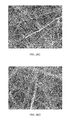
- 238000001878 scanning electron micrograph Methods 0.000 description 7
- 239000004065 semiconductor Substances 0.000 description 6
- 238000011282 treatment Methods 0.000 description 6
- XLYOFNOQVPJJNP-UHFFFAOYSA-N water Substances O XLYOFNOQVPJJNP-UHFFFAOYSA-N 0.000 description 6
- 238000001816 cooling Methods 0.000 description 5
- 230000005496 eutectics Effects 0.000 description 5
- 238000010438 heat treatment Methods 0.000 description 5
- 238000011068 loading method Methods 0.000 description 5
- 230000000737 periodic effect Effects 0.000 description 5
- 229910000077 silane Inorganic materials 0.000 description 5
- 229910007264 Si2H6 Inorganic materials 0.000 description 4
- 125000004429 atom Chemical group 0.000 description 4
- PZPGRFITIJYNEJ-UHFFFAOYSA-N disilane Chemical compound [SiH3][SiH3] PZPGRFITIJYNEJ-UHFFFAOYSA-N 0.000 description 4
- 229910052711 selenium Inorganic materials 0.000 description 4
- 229910052714 tellurium Inorganic materials 0.000 description 4
- OKTJSMMVPCPJKN-UHFFFAOYSA-N Carbon Chemical compound [C] OKTJSMMVPCPJKN-UHFFFAOYSA-N 0.000 description 3
- XUIMIQQOPSSXEZ-UHFFFAOYSA-N Silicon Chemical compound [Si] XUIMIQQOPSSXEZ-UHFFFAOYSA-N 0.000 description 3
- 239000007900 aqueous suspension Substances 0.000 description 3
- 230000008901 benefit Effects 0.000 description 3
- 238000004140 cleaning Methods 0.000 description 3
- 238000000354 decomposition reaction Methods 0.000 description 3
- 238000001914 filtration Methods 0.000 description 3
- 229910052733 gallium Inorganic materials 0.000 description 3
- -1 gold Chemical class 0.000 description 3
- 229910052738 indium Inorganic materials 0.000 description 3
- XEEYBQQBJWHFJM-UHFFFAOYSA-N iron Substances [Fe] XEEYBQQBJWHFJM-UHFFFAOYSA-N 0.000 description 3
- 239000007788 liquid Substances 0.000 description 3
- 230000000873 masking effect Effects 0.000 description 3
- 150000002739 metals Chemical class 0.000 description 3
- 239000002074 nanoribbon Substances 0.000 description 3
- 239000002073 nanorod Substances 0.000 description 3
- 238000000059 patterning Methods 0.000 description 3
- 239000010703 silicon Substances 0.000 description 3
- 239000010935 stainless steel Substances 0.000 description 3
- 229910001220 stainless steel Inorganic materials 0.000 description 3
- 229910052717 sulfur Inorganic materials 0.000 description 3
- 229910052718 tin Inorganic materials 0.000 description 3
- VEXZGXHMUGYJMC-UHFFFAOYSA-N Hydrochloric acid Chemical compound Cl VEXZGXHMUGYJMC-UHFFFAOYSA-N 0.000 description 2
- PXHVJJICTQNCMI-UHFFFAOYSA-N Nickel Chemical compound [Ni] PXHVJJICTQNCMI-UHFFFAOYSA-N 0.000 description 2
- KDLHZDBZIXYQEI-UHFFFAOYSA-N Palladium Chemical compound [Pd] KDLHZDBZIXYQEI-UHFFFAOYSA-N 0.000 description 2
- 108010039918 Polylysine Proteins 0.000 description 2
- 229910045601 alloy Inorganic materials 0.000 description 2
- 239000000956 alloy Substances 0.000 description 2
- VXAUWWUXCIMFIM-UHFFFAOYSA-M aluminum;oxygen(2-);hydroxide Chemical compound [OH-].[O-2].[Al+3] VXAUWWUXCIMFIM-UHFFFAOYSA-M 0.000 description 2
- 238000000231 atomic layer deposition Methods 0.000 description 2
- 230000015572 biosynthetic process Effects 0.000 description 2
- 229910052796 boron Inorganic materials 0.000 description 2
- 229910052799 carbon Inorganic materials 0.000 description 2
- 239000002041 carbon nanotube Substances 0.000 description 2
- 229910021393 carbon nanotube Inorganic materials 0.000 description 2
- 125000001309 chloro group Chemical group Cl* 0.000 description 2
- 238000000576 coating method Methods 0.000 description 2
- 238000004891 communication Methods 0.000 description 2
- 229910052802 copper Inorganic materials 0.000 description 2
- 239000010949 copper Substances 0.000 description 2
- 238000005516 engineering process Methods 0.000 description 2
- 239000012530 fluid Substances 0.000 description 2
- 239000000446 fuel Substances 0.000 description 2
- 229910052732 germanium Inorganic materials 0.000 description 2
- 239000011521 glass Substances 0.000 description 2
- 230000033444 hydroxylation Effects 0.000 description 2
- 238000005805 hydroxylation reaction Methods 0.000 description 2
- 229910052742 iron Inorganic materials 0.000 description 2
- 239000000155 melt Substances 0.000 description 2
- 238000002844 melting Methods 0.000 description 2
- 230000008018 melting Effects 0.000 description 2
- 239000002086 nanomaterial Substances 0.000 description 2
- 230000003647 oxidation Effects 0.000 description 2
- 238000007254 oxidation reaction Methods 0.000 description 2
- 229910052698 phosphorus Inorganic materials 0.000 description 2
- XHXFXVLFKHQFAL-UHFFFAOYSA-N phosphoryl trichloride Chemical compound ClP(Cl)(Cl)=O XHXFXVLFKHQFAL-UHFFFAOYSA-N 0.000 description 2
- BASFCYQUMIYNBI-UHFFFAOYSA-N platinum Chemical compound [Pt] BASFCYQUMIYNBI-UHFFFAOYSA-N 0.000 description 2
- 229920000656 polylysine Polymers 0.000 description 2
- 229920000642 polymer Polymers 0.000 description 2
- 239000000843 powder Substances 0.000 description 2
- 229910010271 silicon carbide Inorganic materials 0.000 description 2
- 229910052709 silver Inorganic materials 0.000 description 2
- 239000007787 solid Substances 0.000 description 2
- 239000007921 spray Substances 0.000 description 2
- 239000000126 substance Substances 0.000 description 2
- 239000000725 suspension Substances 0.000 description 2
- 238000001308 synthesis method Methods 0.000 description 2
- 238000003786 synthesis reaction Methods 0.000 description 2
- YBNMDCCMCLUHBL-UHFFFAOYSA-N (2,5-dioxopyrrolidin-1-yl) 4-pyren-1-ylbutanoate Chemical compound C=1C=C(C2=C34)C=CC3=CC=CC4=CC=C2C=1CCCC(=O)ON1C(=O)CCC1=O YBNMDCCMCLUHBL-UHFFFAOYSA-N 0.000 description 1
- 229910017115 AlSb Inorganic materials 0.000 description 1
- 229910015849 BeSiN2 Inorganic materials 0.000 description 1
- 229910015894 BeTe Inorganic materials 0.000 description 1
- 229910004608 CdSnAs2 Inorganic materials 0.000 description 1
- 229910004613 CdTe Inorganic materials 0.000 description 1
- VYZAMTAEIAYCRO-UHFFFAOYSA-N Chromium Chemical compound [Cr] VYZAMTAEIAYCRO-UHFFFAOYSA-N 0.000 description 1
- RYGMFSIKBFXOCR-UHFFFAOYSA-N Copper Chemical compound [Cu] RYGMFSIKBFXOCR-UHFFFAOYSA-N 0.000 description 1
- 229910021589 Copper(I) bromide Inorganic materials 0.000 description 1
- 229910021591 Copper(I) chloride Inorganic materials 0.000 description 1
- 229910021593 Copper(I) fluoride Inorganic materials 0.000 description 1
- 229910021595 Copper(I) iodide Inorganic materials 0.000 description 1
- VMQMZMRVKUZKQL-UHFFFAOYSA-N Cu+ Chemical compound [Cu+] VMQMZMRVKUZKQL-UHFFFAOYSA-N 0.000 description 1
- 229910016518 CuGeP3 Inorganic materials 0.000 description 1
- 229910016351 CuSi2P3 Inorganic materials 0.000 description 1
- 229910002601 GaN Inorganic materials 0.000 description 1
- 229910005540 GaP Inorganic materials 0.000 description 1
- 229910005542 GaSb Inorganic materials 0.000 description 1
- GYHNNYVSQQEPJS-UHFFFAOYSA-N Gallium Chemical compound [Ga] GYHNNYVSQQEPJS-UHFFFAOYSA-N 0.000 description 1
- 229910001218 Gallium arsenide Inorganic materials 0.000 description 1
- 229910005987 Ge3N4 Inorganic materials 0.000 description 1
- 229910005829 GeS Inorganic materials 0.000 description 1
- 229910005866 GeSe Inorganic materials 0.000 description 1
- 229910005900 GeTe Inorganic materials 0.000 description 1
- 229910005939 Ge—Sn Inorganic materials 0.000 description 1
- 229910004042 HAuCl4 Inorganic materials 0.000 description 1
- 229910004262 HgTe Inorganic materials 0.000 description 1
- UFHFLCQGNIYNRP-UHFFFAOYSA-N Hydrogen Chemical compound [H][H] UFHFLCQGNIYNRP-UHFFFAOYSA-N 0.000 description 1
- 229910000673 Indium arsenide Inorganic materials 0.000 description 1
- GPXJNWSHGFTCBW-UHFFFAOYSA-N Indium phosphide Chemical compound [In]#P GPXJNWSHGFTCBW-UHFFFAOYSA-N 0.000 description 1
- ZOKXTWBITQBERF-UHFFFAOYSA-N Molybdenum Chemical compound [Mo] ZOKXTWBITQBERF-UHFFFAOYSA-N 0.000 description 1
- 229910019213 POCl3 Inorganic materials 0.000 description 1
- 229910002665 PbTe Inorganic materials 0.000 description 1
- KJTLSVCANCCWHF-UHFFFAOYSA-N Ruthenium Chemical compound [Ru] KJTLSVCANCCWHF-UHFFFAOYSA-N 0.000 description 1
- 229910018540 Si C Inorganic materials 0.000 description 1
- 229910008045 Si-Si Inorganic materials 0.000 description 1
- 229910008355 Si-Sn Inorganic materials 0.000 description 1
- 229910052581 Si3N4 Inorganic materials 0.000 description 1
- BQCADISMDOOEFD-UHFFFAOYSA-N Silver Chemical compound [Ag] BQCADISMDOOEFD-UHFFFAOYSA-N 0.000 description 1
- 229910021607 Silver chloride Inorganic materials 0.000 description 1
- 229910021608 Silver(I) fluoride Inorganic materials 0.000 description 1
- 229910008310 Si—Ge Inorganic materials 0.000 description 1
- 229910006411 Si—Si Inorganic materials 0.000 description 1
- 229910006453 Si—Sn Inorganic materials 0.000 description 1
- 229910005642 SnTe Inorganic materials 0.000 description 1
- ATJFFYVFTNAWJD-UHFFFAOYSA-N Tin Chemical compound [Sn] ATJFFYVFTNAWJD-UHFFFAOYSA-N 0.000 description 1
- RTAQQCXQSZGOHL-UHFFFAOYSA-N Titanium Chemical compound [Ti] RTAQQCXQSZGOHL-UHFFFAOYSA-N 0.000 description 1
- XLOMVQKBTHCTTD-UHFFFAOYSA-N Zinc monoxide Chemical compound [Zn]=O XLOMVQKBTHCTTD-UHFFFAOYSA-N 0.000 description 1
- QCWXUUIWCKQGHC-UHFFFAOYSA-N Zirconium Chemical compound [Zr] QCWXUUIWCKQGHC-UHFFFAOYSA-N 0.000 description 1
- 229910007475 ZnGeP2 Inorganic materials 0.000 description 1
- 229910007707 ZnSnSb2 Inorganic materials 0.000 description 1
- 229910007709 ZnTe Inorganic materials 0.000 description 1
- 230000006978 adaptation Effects 0.000 description 1
- 239000000654 additive Substances 0.000 description 1
- 239000012790 adhesive layer Substances 0.000 description 1
- RREGISFBPQOLTM-UHFFFAOYSA-N alumane;trihydrate Chemical compound O.O.O.[AlH3] RREGISFBPQOLTM-UHFFFAOYSA-N 0.000 description 1
- 229910052787 antimony Inorganic materials 0.000 description 1
- 229910052785 arsenic Inorganic materials 0.000 description 1
- 239000013590 bulk material Substances 0.000 description 1
- 229910052793 cadmium Inorganic materials 0.000 description 1
- UHYPYGJEEGLRJD-UHFFFAOYSA-N cadmium(2+);selenium(2-) Chemical compound [Se-2].[Cd+2] UHYPYGJEEGLRJD-UHFFFAOYSA-N 0.000 description 1
- 239000006229 carbon black Substances 0.000 description 1
- 239000012159 carrier gas Substances 0.000 description 1
- 230000003197 catalytic effect Effects 0.000 description 1
- 239000000919 ceramic Substances 0.000 description 1
- 229910052804 chromium Inorganic materials 0.000 description 1
- 239000011651 chromium Substances 0.000 description 1
- 239000011248 coating agent Substances 0.000 description 1
- 229910017052 cobalt Inorganic materials 0.000 description 1
- 239000010941 cobalt Substances 0.000 description 1
- GUTLYIVDDKVIGB-UHFFFAOYSA-N cobalt atom Chemical compound [Co] GUTLYIVDDKVIGB-UHFFFAOYSA-N 0.000 description 1
- OXBLHERUFWYNTN-UHFFFAOYSA-M copper(I) chloride Chemical compound [Cu]Cl OXBLHERUFWYNTN-UHFFFAOYSA-M 0.000 description 1
- 229910052593 corundum Inorganic materials 0.000 description 1
- 229910021419 crystalline silicon Inorganic materials 0.000 description 1
- 229910003460 diamond Inorganic materials 0.000 description 1
- 239000010432 diamond Substances 0.000 description 1
- 238000009792 diffusion process Methods 0.000 description 1
- 239000012895 dilution Substances 0.000 description 1
- 238000010790 dilution Methods 0.000 description 1
- 239000004205 dimethyl polysiloxane Substances 0.000 description 1
- 238000003618 dip coating Methods 0.000 description 1
- 238000010494 dissociation reaction Methods 0.000 description 1
- 230000005593 dissociations Effects 0.000 description 1
- 238000001962 electrophoresis Methods 0.000 description 1
- 238000005530 etching Methods 0.000 description 1
- 238000011010 flushing procedure Methods 0.000 description 1
- 239000001307 helium Substances 0.000 description 1
- 229910052734 helium Inorganic materials 0.000 description 1
- SWQJXJOGLNCZEY-UHFFFAOYSA-N helium atom Chemical compound [He] SWQJXJOGLNCZEY-UHFFFAOYSA-N 0.000 description 1
- 229910052739 hydrogen Inorganic materials 0.000 description 1
- 239000001257 hydrogen Substances 0.000 description 1
- 238000007654 immersion Methods 0.000 description 1
- WPYVAWXEWQSOGY-UHFFFAOYSA-N indium antimonide Chemical compound [Sb]#[In] WPYVAWXEWQSOGY-UHFFFAOYSA-N 0.000 description 1
- RPQDHPTXJYYUPQ-UHFFFAOYSA-N indium arsenide Chemical compound [In]#[As] RPQDHPTXJYYUPQ-UHFFFAOYSA-N 0.000 description 1
- 230000000977 initiatory effect Effects 0.000 description 1
- 238000009413 insulation Methods 0.000 description 1
- 229910052741 iridium Inorganic materials 0.000 description 1
- GKOZUEZYRPOHIO-UHFFFAOYSA-N iridium atom Chemical compound [Ir] GKOZUEZYRPOHIO-UHFFFAOYSA-N 0.000 description 1
- 229910052749 magnesium Inorganic materials 0.000 description 1
- WPBNNNQJVZRUHP-UHFFFAOYSA-L manganese(2+);methyl n-[[2-(methoxycarbonylcarbamothioylamino)phenyl]carbamothioyl]carbamate;n-[2-(sulfidocarbothioylamino)ethyl]carbamodithioate Chemical compound [Mn+2].[S-]C(=S)NCCNC([S-])=S.COC(=O)NC(=S)NC1=CC=CC=C1NC(=S)NC(=O)OC WPBNNNQJVZRUHP-UHFFFAOYSA-L 0.000 description 1
- 229910052753 mercury Inorganic materials 0.000 description 1
- 238000001465 metallisation Methods 0.000 description 1
- 238000001000 micrograph Methods 0.000 description 1
- 230000004048 modification Effects 0.000 description 1
- 238000012986 modification Methods 0.000 description 1
- 229910003465 moissanite Inorganic materials 0.000 description 1
- 229910052750 molybdenum Inorganic materials 0.000 description 1
- 239000011733 molybdenum Substances 0.000 description 1
- 239000002159 nanocrystal Substances 0.000 description 1
- 229910052759 nickel Inorganic materials 0.000 description 1
- 229910052758 niobium Inorganic materials 0.000 description 1
- 239000010955 niobium Substances 0.000 description 1
- GUCVJGMIXFAOAE-UHFFFAOYSA-N niobium atom Chemical compound [Nb] GUCVJGMIXFAOAE-UHFFFAOYSA-N 0.000 description 1
- 230000003287 optical effect Effects 0.000 description 1
- 238000005457 optimization Methods 0.000 description 1
- 229920000620 organic polymer Polymers 0.000 description 1
- 229910052762 osmium Inorganic materials 0.000 description 1
- SYQBFIAQOQZEGI-UHFFFAOYSA-N osmium atom Chemical compound [Os] SYQBFIAQOQZEGI-UHFFFAOYSA-N 0.000 description 1
- 238000000643 oven drying Methods 0.000 description 1
- 229910052763 palladium Inorganic materials 0.000 description 1
- SLIUAWYAILUBJU-UHFFFAOYSA-N pentacene Chemical compound C1=CC=CC2=CC3=CC4=CC5=CC=CC=C5C=C4C=C3C=C21 SLIUAWYAILUBJU-UHFFFAOYSA-N 0.000 description 1
- 238000010587 phase diagram Methods 0.000 description 1
- 229910052697 platinum Inorganic materials 0.000 description 1
- 229920000435 poly(dimethylsiloxane) Polymers 0.000 description 1
- 239000002861 polymer material Substances 0.000 description 1
- 229910052703 rhodium Inorganic materials 0.000 description 1
- 239000010948 rhodium Substances 0.000 description 1
- MHOVAHRLVXNVSD-UHFFFAOYSA-N rhodium atom Chemical compound [Rh] MHOVAHRLVXNVSD-UHFFFAOYSA-N 0.000 description 1
- 229910052707 ruthenium Inorganic materials 0.000 description 1
- 238000004626 scanning electron microscopy Methods 0.000 description 1
- SBIBMFFZSBJNJF-UHFFFAOYSA-N selenium;zinc Chemical compound [Se]=[Zn] SBIBMFFZSBJNJF-UHFFFAOYSA-N 0.000 description 1
- 239000004332 silver Substances 0.000 description 1
- ADZWSOLPGZMUMY-UHFFFAOYSA-M silver bromide Chemical compound [Ag]Br ADZWSOLPGZMUMY-UHFFFAOYSA-M 0.000 description 1
- HKZLPVFGJNLROG-UHFFFAOYSA-M silver monochloride Chemical compound [Cl-].[Ag+] HKZLPVFGJNLROG-UHFFFAOYSA-M 0.000 description 1
- REYHXKZHIMGNSE-UHFFFAOYSA-M silver monofluoride Chemical compound [F-].[Ag+] REYHXKZHIMGNSE-UHFFFAOYSA-M 0.000 description 1
- 239000002002 slurry Substances 0.000 description 1
- 238000002791 soaking Methods 0.000 description 1
- MBEGFNBBAVRKLK-UHFFFAOYSA-N sodium;iminomethylideneazanide Chemical compound [Na+].[NH-]C#N MBEGFNBBAVRKLK-UHFFFAOYSA-N 0.000 description 1
- 239000002904 solvent Substances 0.000 description 1
- 238000005507 spraying Methods 0.000 description 1
- 238000004544 sputter deposition Methods 0.000 description 1
- 238000010189 synthetic method Methods 0.000 description 1
- 229910052715 tantalum Inorganic materials 0.000 description 1
- GUVRBAGPIYLISA-UHFFFAOYSA-N tantalum atom Chemical compound [Ta] GUVRBAGPIYLISA-UHFFFAOYSA-N 0.000 description 1
- OCGWQDWYSQAFTO-UHFFFAOYSA-N tellanylidenelead Chemical compound [Pb]=[Te] OCGWQDWYSQAFTO-UHFFFAOYSA-N 0.000 description 1
- 229910052716 thallium Inorganic materials 0.000 description 1
- 239000010409 thin film Substances 0.000 description 1
- 229910052719 titanium Inorganic materials 0.000 description 1
- 239000010936 titanium Substances 0.000 description 1
- 229910052723 transition metal Inorganic materials 0.000 description 1
- 229910000314 transition metal oxide Inorganic materials 0.000 description 1
- 150000003624 transition metals Chemical class 0.000 description 1
- WFKWXMTUELFFGS-UHFFFAOYSA-N tungsten Chemical compound [W] WFKWXMTUELFFGS-UHFFFAOYSA-N 0.000 description 1
- 229910052721 tungsten Inorganic materials 0.000 description 1
- 239000010937 tungsten Substances 0.000 description 1
- 238000011144 upstream manufacturing Methods 0.000 description 1
- 229910052720 vanadium Inorganic materials 0.000 description 1
- LEONUFNNVUYDNQ-UHFFFAOYSA-N vanadium atom Chemical compound [V] LEONUFNNVUYDNQ-UHFFFAOYSA-N 0.000 description 1
- 235000012431 wafers Nutrition 0.000 description 1
- 229910001845 yogo sapphire Inorganic materials 0.000 description 1
- 229910052725 zinc Inorganic materials 0.000 description 1
- 229910052726 zirconium Inorganic materials 0.000 description 1
Images


Classifications
-
- C—CHEMISTRY; METALLURGY
- C30—CRYSTAL GROWTH
- C30B—SINGLE-CRYSTAL GROWTH; UNIDIRECTIONAL SOLIDIFICATION OF EUTECTIC MATERIAL OR UNIDIRECTIONAL DEMIXING OF EUTECTOID MATERIAL; REFINING BY ZONE-MELTING OF MATERIAL; PRODUCTION OF A HOMOGENEOUS POLYCRYSTALLINE MATERIAL WITH DEFINED STRUCTURE; SINGLE CRYSTALS OR HOMOGENEOUS POLYCRYSTALLINE MATERIAL WITH DEFINED STRUCTURE; AFTER-TREATMENT OF SINGLE CRYSTALS OR A HOMOGENEOUS POLYCRYSTALLINE MATERIAL WITH DEFINED STRUCTURE; APPARATUS THEREFOR
- C30B29/00—Single crystals or homogeneous polycrystalline material with defined structure characterised by the material or by their shape
- C30B29/02—Elements
- C30B29/06—Silicon
-
- B—PERFORMING OPERATIONS; TRANSPORTING
- B01—PHYSICAL OR CHEMICAL PROCESSES OR APPARATUS IN GENERAL
- B01J—CHEMICAL OR PHYSICAL PROCESSES, e.g. CATALYSIS OR COLLOID CHEMISTRY; THEIR RELEVANT APPARATUS
- B01J19/00—Chemical, physical or physico-chemical processes in general; Their relevant apparatus
- B01J19/0053—Details of the reactor
- B01J19/006—Baffles
-
- B—PERFORMING OPERATIONS; TRANSPORTING
- B01—PHYSICAL OR CHEMICAL PROCESSES OR APPARATUS IN GENERAL
- B01J—CHEMICAL OR PHYSICAL PROCESSES, e.g. CATALYSIS OR COLLOID CHEMISTRY; THEIR RELEVANT APPARATUS
- B01J19/00—Chemical, physical or physico-chemical processes in general; Their relevant apparatus
- B01J19/24—Stationary reactors without moving elements inside
- B01J19/2415—Tubular reactors
-
- B—PERFORMING OPERATIONS; TRANSPORTING
- B01—PHYSICAL OR CHEMICAL PROCESSES OR APPARATUS IN GENERAL
- B01J—CHEMICAL OR PHYSICAL PROCESSES, e.g. CATALYSIS OR COLLOID CHEMISTRY; THEIR RELEVANT APPARATUS
- B01J19/00—Chemical, physical or physico-chemical processes in general; Their relevant apparatus
- B01J19/24—Stationary reactors without moving elements inside
- B01J19/248—Reactors comprising multiple separated flow channels
- B01J19/2495—Net-type reactors
-
- B—PERFORMING OPERATIONS; TRANSPORTING
- B01—PHYSICAL OR CHEMICAL PROCESSES OR APPARATUS IN GENERAL
- B01J—CHEMICAL OR PHYSICAL PROCESSES, e.g. CATALYSIS OR COLLOID CHEMISTRY; THEIR RELEVANT APPARATUS
- B01J19/00—Chemical, physical or physico-chemical processes in general; Their relevant apparatus
- B01J19/32—Packing elements in the form of grids or built-up elements for forming a unit or module inside the apparatus for mass or heat transfer
-
- B—PERFORMING OPERATIONS; TRANSPORTING
- B01—PHYSICAL OR CHEMICAL PROCESSES OR APPARATUS IN GENERAL
- B01J—CHEMICAL OR PHYSICAL PROCESSES, e.g. CATALYSIS OR COLLOID CHEMISTRY; THEIR RELEVANT APPARATUS
- B01J23/00—Catalysts comprising metals or metal oxides or hydroxides, not provided for in group B01J21/00
- B01J23/38—Catalysts comprising metals or metal oxides or hydroxides, not provided for in group B01J21/00 of noble metals
- B01J23/48—Silver or gold
- B01J23/52—Gold
-
- B01J35/23—
-
- B01J35/56—
-
- B—PERFORMING OPERATIONS; TRANSPORTING
- B01—PHYSICAL OR CHEMICAL PROCESSES OR APPARATUS IN GENERAL
- B01J—CHEMICAL OR PHYSICAL PROCESSES, e.g. CATALYSIS OR COLLOID CHEMISTRY; THEIR RELEVANT APPARATUS
- B01J37/00—Processes, in general, for preparing catalysts; Processes, in general, for activation of catalysts
- B01J37/02—Impregnation, coating or precipitation
- B01J37/0201—Impregnation
- B01J37/0207—Pretreatment of the support
-
- B—PERFORMING OPERATIONS; TRANSPORTING
- B01—PHYSICAL OR CHEMICAL PROCESSES OR APPARATUS IN GENERAL
- B01J—CHEMICAL OR PHYSICAL PROCESSES, e.g. CATALYSIS OR COLLOID CHEMISTRY; THEIR RELEVANT APPARATUS
- B01J37/00—Processes, in general, for preparing catalysts; Processes, in general, for activation of catalysts
- B01J37/02—Impregnation, coating or precipitation
- B01J37/0201—Impregnation
- B01J37/0211—Impregnation using a colloidal suspension
-
- B—PERFORMING OPERATIONS; TRANSPORTING
- B01—PHYSICAL OR CHEMICAL PROCESSES OR APPARATUS IN GENERAL
- B01J—CHEMICAL OR PHYSICAL PROCESSES, e.g. CATALYSIS OR COLLOID CHEMISTRY; THEIR RELEVANT APPARATUS
- B01J37/00—Processes, in general, for preparing catalysts; Processes, in general, for activation of catalysts
- B01J37/02—Impregnation, coating or precipitation
- B01J37/0215—Coating
- B01J37/0217—Pretreatment of the substrate before coating
-
- B—PERFORMING OPERATIONS; TRANSPORTING
- B01—PHYSICAL OR CHEMICAL PROCESSES OR APPARATUS IN GENERAL
- B01J—CHEMICAL OR PHYSICAL PROCESSES, e.g. CATALYSIS OR COLLOID CHEMISTRY; THEIR RELEVANT APPARATUS
- B01J37/00—Processes, in general, for preparing catalysts; Processes, in general, for activation of catalysts
- B01J37/02—Impregnation, coating or precipitation
- B01J37/0215—Coating
- B01J37/0225—Coating of metal substrates
-
- B—PERFORMING OPERATIONS; TRANSPORTING
- B82—NANOTECHNOLOGY
- B82Y—SPECIFIC USES OR APPLICATIONS OF NANOSTRUCTURES; MEASUREMENT OR ANALYSIS OF NANOSTRUCTURES; MANUFACTURE OR TREATMENT OF NANOSTRUCTURES
- B82Y30/00—Nanotechnology for materials or surface science, e.g. nanocomposites
-
- B—PERFORMING OPERATIONS; TRANSPORTING
- B82—NANOTECHNOLOGY
- B82Y—SPECIFIC USES OR APPLICATIONS OF NANOSTRUCTURES; MEASUREMENT OR ANALYSIS OF NANOSTRUCTURES; MANUFACTURE OR TREATMENT OF NANOSTRUCTURES
- B82Y40/00—Manufacture or treatment of nanostructures
-
- C—CHEMISTRY; METALLURGY
- C01—INORGANIC CHEMISTRY
- C01B—NON-METALLIC ELEMENTS; COMPOUNDS THEREOF; METALLOIDS OR COMPOUNDS THEREOF NOT COVERED BY SUBCLASS C01C
- C01B32/00—Carbon; Compounds thereof
- C01B32/15—Nano-sized carbon materials
-
- C—CHEMISTRY; METALLURGY
- C30—CRYSTAL GROWTH
- C30B—SINGLE-CRYSTAL GROWTH; UNIDIRECTIONAL SOLIDIFICATION OF EUTECTIC MATERIAL OR UNIDIRECTIONAL DEMIXING OF EUTECTOID MATERIAL; REFINING BY ZONE-MELTING OF MATERIAL; PRODUCTION OF A HOMOGENEOUS POLYCRYSTALLINE MATERIAL WITH DEFINED STRUCTURE; SINGLE CRYSTALS OR HOMOGENEOUS POLYCRYSTALLINE MATERIAL WITH DEFINED STRUCTURE; AFTER-TREATMENT OF SINGLE CRYSTALS OR A HOMOGENEOUS POLYCRYSTALLINE MATERIAL WITH DEFINED STRUCTURE; APPARATUS THEREFOR
- C30B11/00—Single-crystal growth by normal freezing or freezing under temperature gradient, e.g. Bridgman-Stockbarger method
- C30B11/04—Single-crystal growth by normal freezing or freezing under temperature gradient, e.g. Bridgman-Stockbarger method adding crystallising materials or reactants forming it in situ to the melt
- C30B11/08—Single-crystal growth by normal freezing or freezing under temperature gradient, e.g. Bridgman-Stockbarger method adding crystallising materials or reactants forming it in situ to the melt every component of the crystal composition being added during the crystallisation
- C30B11/12—Vaporous components, e.g. vapour-liquid-solid-growth
-
- C—CHEMISTRY; METALLURGY
- C30—CRYSTAL GROWTH
- C30B—SINGLE-CRYSTAL GROWTH; UNIDIRECTIONAL SOLIDIFICATION OF EUTECTIC MATERIAL OR UNIDIRECTIONAL DEMIXING OF EUTECTOID MATERIAL; REFINING BY ZONE-MELTING OF MATERIAL; PRODUCTION OF A HOMOGENEOUS POLYCRYSTALLINE MATERIAL WITH DEFINED STRUCTURE; SINGLE CRYSTALS OR HOMOGENEOUS POLYCRYSTALLINE MATERIAL WITH DEFINED STRUCTURE; AFTER-TREATMENT OF SINGLE CRYSTALS OR A HOMOGENEOUS POLYCRYSTALLINE MATERIAL WITH DEFINED STRUCTURE; APPARATUS THEREFOR
- C30B29/00—Single crystals or homogeneous polycrystalline material with defined structure characterised by the material or by their shape
- C30B29/60—Single crystals or homogeneous polycrystalline material with defined structure characterised by the material or by their shape characterised by shape
- C30B29/602—Nanotubes
-
- B—PERFORMING OPERATIONS; TRANSPORTING
- B01—PHYSICAL OR CHEMICAL PROCESSES OR APPARATUS IN GENERAL
- B01J—CHEMICAL OR PHYSICAL PROCESSES, e.g. CATALYSIS OR COLLOID CHEMISTRY; THEIR RELEVANT APPARATUS
- B01J21/00—Catalysts comprising the elements, oxides, or hydroxides of magnesium, boron, aluminium, carbon, silicon, titanium, zirconium, or hafnium
- B01J21/06—Silicon, titanium, zirconium or hafnium; Oxides or hydroxides thereof
- B01J21/08—Silica
-
- B—PERFORMING OPERATIONS; TRANSPORTING
- B01—PHYSICAL OR CHEMICAL PROCESSES OR APPARATUS IN GENERAL
- B01J—CHEMICAL OR PHYSICAL PROCESSES, e.g. CATALYSIS OR COLLOID CHEMISTRY; THEIR RELEVANT APPARATUS
- B01J21/00—Catalysts comprising the elements, oxides, or hydroxides of magnesium, boron, aluminium, carbon, silicon, titanium, zirconium, or hafnium
- B01J21/18—Carbon
- B01J21/185—Carbon nanotubes
-
- B—PERFORMING OPERATIONS; TRANSPORTING
- B01—PHYSICAL OR CHEMICAL PROCESSES OR APPARATUS IN GENERAL
- B01J—CHEMICAL OR PHYSICAL PROCESSES, e.g. CATALYSIS OR COLLOID CHEMISTRY; THEIR RELEVANT APPARATUS
- B01J2219/00—Chemical, physical or physico-chemical processes in general; Their relevant apparatus
- B01J2219/00761—Details of the reactor
- B01J2219/00763—Baffles
- B01J2219/00765—Baffles attached to the reactor wall
- B01J2219/0077—Baffles attached to the reactor wall inclined
- B01J2219/00772—Baffles attached to the reactor wall inclined in a helix
-
- B—PERFORMING OPERATIONS; TRANSPORTING
- B01—PHYSICAL OR CHEMICAL PROCESSES OR APPARATUS IN GENERAL
- B01J—CHEMICAL OR PHYSICAL PROCESSES, e.g. CATALYSIS OR COLLOID CHEMISTRY; THEIR RELEVANT APPARATUS
- B01J2219/00—Chemical, physical or physico-chemical processes in general; Their relevant apparatus
- B01J2219/32—Details relating to packing elements in the form of grids or built-up elements for forming a unit of module inside the apparatus for mass or heat transfer
- B01J2219/324—Composition or microstructure of the elements
- B01J2219/32466—Composition or microstructure of the elements comprising catalytically active material
-
- B—PERFORMING OPERATIONS; TRANSPORTING
- B01—PHYSICAL OR CHEMICAL PROCESSES OR APPARATUS IN GENERAL
- B01J—CHEMICAL OR PHYSICAL PROCESSES, e.g. CATALYSIS OR COLLOID CHEMISTRY; THEIR RELEVANT APPARATUS
- B01J2219/00—Chemical, physical or physico-chemical processes in general; Their relevant apparatus
- B01J2219/32—Details relating to packing elements in the form of grids or built-up elements for forming a unit of module inside the apparatus for mass or heat transfer
- B01J2219/324—Composition or microstructure of the elements
- B01J2219/32491—Woven or knitted materials
-
- B01J35/31—
-
- B01J35/58—
-
- D—TEXTILES; PAPER
- D01—NATURAL OR MAN-MADE THREADS OR FIBRES; SPINNING
- D01F—CHEMICAL FEATURES IN THE MANUFACTURE OF ARTIFICIAL FILAMENTS, THREADS, FIBRES, BRISTLES OR RIBBONS; APPARATUS SPECIALLY ADAPTED FOR THE MANUFACTURE OF CARBON FILAMENTS
- D01F9/00—Artificial filaments or the like of other substances; Manufacture thereof; Apparatus specially adapted for the manufacture of carbon filaments
Landscapes
- Chemical & Material Sciences (AREA)
- Engineering & Computer Science (AREA)
- Organic Chemistry (AREA)
- Materials Engineering (AREA)
- Chemical Kinetics & Catalysis (AREA)
- Nanotechnology (AREA)
- Crystallography & Structural Chemistry (AREA)
- Physics & Mathematics (AREA)
- Metallurgy (AREA)
- Condensed Matter Physics & Semiconductors (AREA)
- General Physics & Mathematics (AREA)
- Thermal Sciences (AREA)
- Inorganic Chemistry (AREA)
- Manufacturing & Machinery (AREA)
- Composite Materials (AREA)
- Catalysts (AREA)
Abstract
Description
| TABLE 1 | |||
| Run# 202- | |||
| -051 | -057 | |||
| 1100-H19 Al foils length (6″ & 8″): | ~11.1 ft | ~9.6 ft | ||
| Au Colloid size (nm) | 60 | 20 | ||
| Au Colloid Deposit Time (hrs in | 5.0 | 4.5 | ||
| diluted 0.01% Au Chloride)** | ||||
| Au NP density (per μm2) | 10.6 | 21.2 | ||
| Tube OD (in) | 3 | 3 | ||
| Surface area (m2): | 2.42 | 2.07 | ||
| NW Growth conditions: | ||||
| Total Pressure (torr): | 30 | 45 | ||
| Silane Partial Pressure (torr): | 1.7 | 4.8 | ||
| Silane Flow (sccm) | 50.2 | 75.2 | ||
| Hydrogen Flow (sccm) | 301 | 234 | ||
| Helium Flow (sccm) | 551 | 401 | ||
| TC Setpoint (° C.) | 455 | 450 | ||
| Total Gas Flow (sccm) | 902 | 711 | ||
| Calc. Gas Residence Time (sec)*** | 0.77 | 1.48 | ||
| Growth Time (min) | 60 | 100 | ||
| NW + Si Deposit wt gain (g): | 2.52 | 1.98 | ||
| (g/m2) | 1.04 | 0.96 | ||
| **Dilutions are 60% for 60 nm and 30% for 20 nm. | ||||
| ***neglecting cross-sectional area occupied by the foils | ||||
Claims (13)
Priority Applications (1)
| Application Number | Priority Date | Filing Date | Title |
|---|---|---|---|
| US12/824,485 US8623288B1 (en) | 2009-06-29 | 2010-06-28 | Apparatus and methods for high density nanowire growth |
Applications Claiming Priority (2)
| Application Number | Priority Date | Filing Date | Title |
|---|---|---|---|
| US22150109P | 2009-06-29 | 2009-06-29 | |
| US12/824,485 US8623288B1 (en) | 2009-06-29 | 2010-06-28 | Apparatus and methods for high density nanowire growth |
Publications (1)
| Publication Number | Publication Date |
|---|---|
| US8623288B1 true US8623288B1 (en) | 2014-01-07 |
Family
ID=49840828
Family Applications (1)
| Application Number | Title | Priority Date | Filing Date |
|---|---|---|---|
| US12/824,485 Active 2032-11-07 US8623288B1 (en) | 2009-06-29 | 2010-06-28 | Apparatus and methods for high density nanowire growth |
Country Status (1)
| Country | Link |
|---|---|
| US (1) | US8623288B1 (en) |
Cited By (5)
| Publication number | Priority date | Publication date | Assignee | Title |
|---|---|---|---|---|
| US20090255222A1 (en) * | 2007-07-10 | 2009-10-15 | Raul Cortez | Methods and apparatus for the in situ collection of nucleated particles |
| US20130092525A1 (en) * | 2007-07-10 | 2013-04-18 | Innovalight, Inc. | Concentric flow-through plasma reactor and methods therefor |
| US9812699B2 (en) | 2011-10-05 | 2017-11-07 | Oned Material Llc | Silicon nanostructure active materials for lithium ion batteries and processes, compositions, components and devices related thereto |
| US10243207B2 (en) | 2011-07-26 | 2019-03-26 | Oned Material Llc | Nanostructured battery active materials and methods of producing same |
| US10862114B2 (en) | 2016-07-15 | 2020-12-08 | Oned Material Llc | Manufacturing apparatus and method for making silicon nanowires on carbon based powders for use in batteries |
Citations (118)
| Publication number | Priority date | Publication date | Assignee | Title |
|---|---|---|---|---|
| US5196396A (en) | 1991-07-16 | 1993-03-23 | The President And Fellows Of Harvard College | Method of making a superconducting fullerene composition by reacting a fullerene with an alloy containing alkali metal |
| US5332910A (en) | 1991-03-22 | 1994-07-26 | Hitachi, Ltd. | Semiconductor optical device with nanowhiskers |
| US5505928A (en) | 1991-11-22 | 1996-04-09 | The Regents Of University Of California | Preparation of III-V semiconductor nanocrystals |
| US5512131A (en) | 1993-10-04 | 1996-04-30 | President And Fellows Of Harvard College | Formation of microstamped patterns on surfaces and derivative articles |
| US5674592A (en) | 1995-05-04 | 1997-10-07 | Minnesota Mining And Manufacturing Company | Functionalized nanostructured films |
| US5690807A (en) | 1995-08-03 | 1997-11-25 | Massachusetts Institute Of Technology | Method for producing semiconductor particles |
| US5840435A (en) | 1993-07-15 | 1998-11-24 | President And Fellows Of Harvard College | Covalent carbon nitride material comprising C2 N and formation method |
| US5858862A (en) | 1996-09-25 | 1999-01-12 | Sony Corporation | Process for producing quantum fine wire |
| US5897945A (en) | 1996-02-26 | 1999-04-27 | President And Fellows Of Harvard College | Metal oxide nanorods |
| US5962863A (en) | 1993-09-09 | 1999-10-05 | The United States Of America As Represented By The Secretary Of The Navy | Laterally disposed nanostructures of silicon on an insulating substrate |
| US5976957A (en) | 1996-10-28 | 1999-11-02 | Sony Corporation | Method of making silicon quantum wires on a substrate |
| US5997832A (en) | 1997-03-07 | 1999-12-07 | President And Fellows Of Harvard College | Preparation of carbide nanorods |
| US6036774A (en) | 1996-02-26 | 2000-03-14 | President And Fellows Of Harvard College | Method of producing metal oxide nanorods |
| US6048616A (en) | 1993-04-21 | 2000-04-11 | Philips Electronics N.A. Corp. | Encapsulated quantum sized doped semiconductor particles and method of manufacturing same |
| US6068800A (en) | 1995-09-07 | 2000-05-30 | The Penn State Research Foundation | Production of nano particles and tubes by laser liquid interaction |
| US6132874A (en) | 1995-08-22 | 2000-10-17 | Rhodia Chimie | Functionalized inorganic oxide hydroxylated carrier and method for preparing same |
| US6136156A (en) | 1996-03-01 | 2000-10-24 | Virginia Commonwealth University | Nanoparticles of silicon oxide alloys |
| US6146227A (en) | 1998-09-28 | 2000-11-14 | Xidex Corporation | Method for manufacturing carbon nanotubes as functional elements of MEMS devices |
| US6190634B1 (en) | 1995-06-07 | 2001-02-20 | President And Fellows Of Harvard College | Carbide nanomaterials |
| US6207229B1 (en) | 1997-11-13 | 2001-03-27 | Massachusetts Institute Of Technology | Highly luminescent color-selective materials and method of making thereof |
| US6225198B1 (en) | 2000-02-04 | 2001-05-01 | The Regents Of The University Of California | Process for forming shaped group II-VI semiconductor nanocrystals, and product formed using process |
| US6235675B1 (en) | 1998-09-22 | 2001-05-22 | Idaho Research Foundation, Inc. | Methods of forming materials containing carbon and boron, methods of forming catalysts, filaments comprising boron and carbon, and catalysts |
| US6256767B1 (en) | 1999-03-29 | 2001-07-03 | Hewlett-Packard Company | Demultiplexer for a molecular wire crossbar network (MWCN DEMUX) |
| US6261469B1 (en) | 1998-10-13 | 2001-07-17 | Honeywell International Inc. | Three dimensionally periodic structural assemblies on nanometer and longer scales |
| US6274007B1 (en) | 1999-11-25 | 2001-08-14 | Sceptre Electronics Limited | Methods of formation of a silicon nanostructure, a silicon quantum wire array and devices based thereon |
| US6294450B1 (en) | 2000-03-01 | 2001-09-25 | Hewlett-Packard Company | Nanoscale patterning for the formation of extensive wires |
| JP2001288626A (en) | 2000-04-03 | 2001-10-19 | Nissan Motor Co Ltd | Method for producing fixed body of carbon nanofiber |
| US6306736B1 (en) | 2000-02-04 | 2001-10-23 | The Regents Of The University Of California | Process for forming shaped group III-V semiconductor nanocrystals, and product formed using process |
| US6306734B1 (en) | 1996-04-01 | 2001-10-23 | Evgeny Invievich Givargizov | Method and apparatus for growing oriented whisker arrays |
| US20010033796A1 (en) | 1999-06-28 | 2001-10-25 | Unger Marc A. | Microfabricated elastomeric valve and pump sysems |
| US20010051367A1 (en) | 1999-04-14 | 2001-12-13 | Ching-Hwa Kiang | Molecular nanowires from single walled carbon nanotubes |
| US20020004136A1 (en) | 1999-06-14 | 2002-01-10 | Yufei Gao | Carbon nanotubes on a substrate |
| US6339281B2 (en) | 2000-01-07 | 2002-01-15 | Samsung Sdi Co., Ltd. | Method for fabricating triode-structure carbon nanotube field emitter array |
| US20020014667A1 (en) | 2000-07-18 | 2002-02-07 | Shin Jin Koog | Method of horizontally growing carbon nanotubes and field effect transistor using the carbon nanotubes grown by the method |
| US6380103B2 (en) | 1996-01-03 | 2002-04-30 | Micron Technology, Inc. | Rapid thermal etch and rapid thermal oxidation |
| US20020072577A1 (en) | 2000-10-04 | 2002-06-13 | The Dow Chemical Company | Supported catalyst compositions |
| US6413489B1 (en) | 1997-04-15 | 2002-07-02 | Massachusetts Institute Of Technology | Synthesis of nanometer-sized particles by reverse micelle mediated techniques |
| US20020127495A1 (en) | 2001-03-12 | 2002-09-12 | Axel Scherer | Method of fabricating nanometer-scale flowchannels and trenches with self-aligned electrodes and the structures formed by the same |
| US20020130353A1 (en) | 1999-07-02 | 2002-09-19 | Lieber Charles M. | Nanoscopic wire-based devices, arrays, and methods of their manufacture |
| US20020130311A1 (en) | 2000-08-22 | 2002-09-19 | Lieber Charles M. | Doped elongated semiconductors, growing such semiconductors, devices including such semiconductors and fabricating such devices |
| US6465132B1 (en) | 1999-07-22 | 2002-10-15 | Agere Systems Guardian Corp. | Article comprising small diameter nanowires and method for making the same |
| US6471761B2 (en) | 2000-04-21 | 2002-10-29 | University Of New Mexico | Prototyping of patterned functional nanostructures |
| US20020158342A1 (en) | 2001-03-14 | 2002-10-31 | Mark Tuominen | Nanofabrication |
| US20020172820A1 (en) | 2001-03-30 | 2002-11-21 | The Regents Of The University Of California | Methods of fabricating nanostructures and nanowires and devices fabricated therefrom |
| US20020179434A1 (en) | 1998-08-14 | 2002-12-05 | The Board Of Trustees Of The Leland Stanford Junior University | Carbon nanotube devices |
| US6495258B1 (en) | 2000-09-20 | 2002-12-17 | Auburn University | Structures with high number density of carbon nanotubes and 3-dimensional distribution |
| US6515325B1 (en) | 2002-03-06 | 2003-02-04 | Micron Technology, Inc. | Nanotube semiconductor devices and methods for making the same |
| US20030037675A1 (en) | 2000-09-05 | 2003-02-27 | Gillingham Gary R. | Air filtration arrangements having fluted media constructions and methods |
| US20030044777A1 (en) | 1993-10-28 | 2003-03-06 | Kenneth L. Beattie | Flowthrough devices for multiple discrete binding reactions |
| US20030071246A1 (en) | 2001-01-23 | 2003-04-17 | Grigorov Leonid N. | Quantum devices based on crystallized electron pairs and methods for their manufacture and use |
| US20030089899A1 (en) | 2000-08-22 | 2003-05-15 | Lieber Charles M. | Nanoscale wires and related devices |
| US6586785B2 (en) | 2000-06-29 | 2003-07-01 | California Institute Of Technology | Aerosol silicon nanoparticles for use in semiconductor device fabrication |
| US20030121887A1 (en) | 2001-03-22 | 2003-07-03 | Garvey James F. | Multi-component substances and processes for preparation thereof |
| US20030184357A1 (en) | 2002-02-19 | 2003-10-02 | Commissariat A L'energie Atomique | Cathode structure with emissive layer formed on a resistive layer |
| US20030185741A1 (en) | 2001-04-06 | 2003-10-02 | Krzysztof Matyjaszewski | Process for the preparation of nanostructured materials |
| US20030186522A1 (en) | 2002-04-02 | 2003-10-02 | Nanosys, Inc. | Methods of positioning and/or orienting nanostructures |
| US20030189202A1 (en) | 2002-04-05 | 2003-10-09 | Jun Li | Nanowire devices and methods of fabrication |
| US20030195611A1 (en) | 2002-04-11 | 2003-10-16 | Greenhalgh Skott E. | Covering and method using electrospinning of very small fibers |
| US20030200521A1 (en) | 2002-01-18 | 2003-10-23 | California Institute Of Technology | Array-based architecture for molecular electronics |
| US6656573B2 (en) | 2001-06-26 | 2003-12-02 | Hewlett-Packard Development Company, L.P. | Method to grow self-assembled epitaxial nanowires |
| US20030222019A1 (en) | 2002-05-28 | 2003-12-04 | Battelle Memorial Institute | Electrostatic deposition of particles generated from rapid expansion of supercritical fluid solutions |
| US20030232721A1 (en) | 2002-01-31 | 2003-12-18 | Hydrocarbon Technologies Inc. | Supported noble metal nanometer catalyst particles containing controlled (111) crystal face exposure |
| US20040005258A1 (en) | 2001-12-12 | 2004-01-08 | Fonash Stephen J. | Chemical reactor templates: sacrificial layer fabrication and template use |
| US20040026684A1 (en) | 2002-04-02 | 2004-02-12 | Nanosys, Inc. | Nanowire heterostructures for encoding information |
| US20040063839A1 (en) | 2002-09-26 | 2004-04-01 | Canon Kabushiki Kaisha | Method of producing electron emitting device using carbon fiber, electron source and image forming apparatus, and ink for producing carbon fiber |
| US20040061422A1 (en) | 2002-09-26 | 2004-04-01 | International Business Machines Corporation | System and method for molecular optical emission |
| US20040095658A1 (en) | 2002-09-05 | 2004-05-20 | Nanosys, Inc. | Nanocomposites |
| US20040112964A1 (en) | 2002-09-30 | 2004-06-17 | Nanosys, Inc. | Applications of nano-enabled large area macroelectronic substrates incorporating nanowires and nanowire composites |
| US20040118448A1 (en) | 2002-09-05 | 2004-06-24 | Nanosys, Inc. | Nanostructure and nanocomposite based compositions and photovoltaic devices |
| US20040121681A1 (en) | 2002-12-23 | 2004-06-24 | Kimberly-Clark Worldwide, Inc. | Absorbent articles containing an activated carbon substrate |
| US20040135951A1 (en) | 2002-09-30 | 2004-07-15 | Dave Stumbo | Integrated displays using nanowire transistors |
| US20040146560A1 (en) | 2002-09-05 | 2004-07-29 | Nanosys, Inc. | Oriented nanostructures and methods of preparing |
| US20040147098A1 (en) | 2002-11-22 | 2004-07-29 | Frederic Mazen | Method for forming, by CVD, nanostructures of semi-conductor material of homogeneous and controlled size on dielectric material |
| US6773616B1 (en) | 2001-11-13 | 2004-08-10 | Hewlett-Packard Development Company, L.P. | Formation of nanoscale wires |
| US6790425B1 (en) | 1999-10-27 | 2004-09-14 | Wiliam Marsh Rice University | Macroscopic ordered assembly of carbon nanotubes |
| US20040206448A1 (en) | 2003-04-17 | 2004-10-21 | Nanosys, Inc. | Structures, systems and methods for joining articles and materials and uses therefor |
| US6808605B2 (en) | 2001-10-15 | 2004-10-26 | Korea Institute Of Science And Technology | Fabrication method of metallic nanowires |
| US20040213307A1 (en) | 2002-07-19 | 2004-10-28 | President And Fellows Of Harvard College | Nanoscale coherent optical components |
| US6831017B1 (en) | 2002-04-05 | 2004-12-14 | Integrated Nanosystems, Inc. | Catalyst patterning for nanowire devices |
| US20050011431A1 (en) | 2003-04-04 | 2005-01-20 | Btg International Limited | Precisely positioned nanowhiskers and nanowhisker arrays and method for preparing them |
| US6846565B2 (en) | 2001-07-02 | 2005-01-25 | Board Of Regents, The University Of Texas System | Light-emitting nanoparticles and method of making same |
| WO2004032193A3 (en) | 2002-09-30 | 2005-01-27 | Nanosys Inc | Large-area nanoenabled macroelectronic substrates and uses therefor |
| US20050026526A1 (en) | 2003-07-30 | 2005-02-03 | Verdegan Barry M. | High performance filter media with internal nanofiber structure and manufacturing methodology |
| US20050029678A1 (en) | 2003-07-08 | 2005-02-10 | University Of Texas System, Board Of Regents | Growth of single crystal nanowires |
| US20050038498A1 (en) | 2003-04-17 | 2005-02-17 | Nanosys, Inc. | Medical device applications of nanostructured surfaces |
| US20050062033A1 (en) | 2003-08-08 | 2005-03-24 | Canon Kabushiki Kaisha | Structure and method for production of the same |
| US20050066883A1 (en) | 2003-09-25 | 2005-03-31 | Nanosys, Inc. | Methods, devices and compositions for depositing and orienting nanostructures |
| US20050079659A1 (en) | 2002-09-30 | 2005-04-14 | Nanosys, Inc. | Large-area nanoenabled macroelectronic substrates and uses therefor |
| US20050089467A1 (en) | 2003-10-22 | 2005-04-28 | International Business Machines Corporation | Control of carbon nanotube diameter using CVD or PECVD growth |
| US6888208B2 (en) | 2003-07-30 | 2005-05-03 | Hewlett-Packard Development Company, L.P. | Square-law detector based on spin injection and nanowires |
| WO2004032191A3 (en) | 2002-09-30 | 2005-06-02 | Nanosys Inc | Applications of nano-enabled large area macroelectronic substrates incorporating nanowires and nanowire composites |
| WO2005023923A3 (en) | 2003-09-04 | 2005-06-16 | Nanosys Inc | Methods of processing nanocrystals, and compositions, devices and systems including same |
| US20050145596A1 (en) | 2003-12-29 | 2005-07-07 | Metz Matthew V. | Method of fabricating multiple nanowires of uniform length from a single catalytic nanoparticle |
| US20050176228A1 (en) | 2003-12-11 | 2005-08-11 | Fonash Stephen J. | Controlled nanowire growth in permanent, integrated nano-templates and methods of fabricating sensor and transducer structures |
| US20050181195A1 (en) | 2003-04-28 | 2005-08-18 | Nanosys, Inc. | Super-hydrophobic surfaces, methods of their construction and uses therefor |
| US20050187605A1 (en) | 2002-04-11 | 2005-08-25 | Greenhalgh Skott E. | Electrospun skin capable of controlling drug release rates and method |
| US20050191774A1 (en) | 2002-10-28 | 2005-09-01 | Zhiyong Li | Photonic crystals with nanowire-based fabrication |
| US20050266662A1 (en) | 2004-05-28 | 2005-12-01 | Yi Sung S | Method of growing semiconductor nanowires with uniform cross-sectional area using chemical vapor deposition |
| US20050279274A1 (en) | 2004-04-30 | 2005-12-22 | Chunming Niu | Systems and methods for nanowire growth and manufacturing |
| US20060008942A1 (en) | 2004-07-07 | 2006-01-12 | Nanosys, Inc. | Systems and methods for harvesting and integrating nanowires |
| US20060006463A1 (en) | 2004-07-09 | 2006-01-12 | Islam M S | Nanowire device with (111) vertical sidewalls and method of fabrication |
| US20060019472A1 (en) | 2004-04-30 | 2006-01-26 | Nanosys, Inc. | Systems and methods for nanowire growth and harvesting |
| US20060019470A1 (en) | 2004-02-06 | 2006-01-26 | Btg International Limited | Directionally controlled growth of nanowhiskers |
| US20060057360A1 (en) | 2003-11-26 | 2006-03-16 | Samuelson Lars I | Nanostructures formed of branched nanowhiskers and methods of producing the same |
| US7057881B2 (en) | 2004-03-18 | 2006-06-06 | Nanosys, Inc | Nanofiber surface based capacitors |
| US20060159916A1 (en) | 2003-05-05 | 2006-07-20 | Nanosys, Inc. | Nanofiber surfaces for use in enhanced surface area applications |
| US20060175601A1 (en) | 2000-08-22 | 2006-08-10 | President And Fellows Of Harvard College | Nanoscale wires and related devices |
| US7091120B2 (en) | 2003-08-04 | 2006-08-15 | Nanosys, Inc. | System and process for producing nanowire composites and electronic substrates therefrom |
| US7097820B2 (en) | 1996-08-08 | 2006-08-29 | William Marsh Rice University | Continuous fiber of single-wall carbon nanotubes |
| US7129554B2 (en) | 2000-12-11 | 2006-10-31 | President & Fellows Of Harvard College | Nanosensors |
| US7135728B2 (en) | 2002-09-30 | 2006-11-14 | Nanosys, Inc. | Large-area nanoenabled macroelectronic substrates and uses therefor |
| US20070004225A1 (en) | 2005-06-30 | 2007-01-04 | Donghui Lu | Low-temperature catalyzed formation of segmented nanowire of dielectric material |
| US20070037365A1 (en) | 2005-08-15 | 2007-02-15 | Ranganath Tirumala R | Semiconductor nanostructures and fabricating the same |
| US20070084797A1 (en) | 2003-03-07 | 2007-04-19 | Seldon Technologies, Llc | Purification of fluids with nanomaterials |
| US7218004B2 (en) | 2005-03-11 | 2007-05-15 | Hewlett-Packard Development Company, L.P. | Fusing nanowires using in situ crystal growth |
| US20080213603A1 (en) * | 2007-03-01 | 2008-09-04 | Nobuhiko Kobayashi | Methods of forming nanostructures on metal-silicide crystallites, and resulting structures and devices |
| US20090311166A1 (en) * | 2006-05-19 | 2009-12-17 | Massachusetts Institute Of Technology | Continuous Process for the Production of Nanostructures Including Nanotubes |
| US7649192B2 (en) | 2005-03-09 | 2010-01-19 | Samsung Electronics Co., Ltd. | Nano wires and method of manufacturing the same |
-
2010
- 2010-06-28 US US12/824,485 patent/US8623288B1/en active Active
Patent Citations (143)
| Publication number | Priority date | Publication date | Assignee | Title |
|---|---|---|---|---|
| US5332910A (en) | 1991-03-22 | 1994-07-26 | Hitachi, Ltd. | Semiconductor optical device with nanowhiskers |
| US5196396A (en) | 1991-07-16 | 1993-03-23 | The President And Fellows Of Harvard College | Method of making a superconducting fullerene composition by reacting a fullerene with an alloy containing alkali metal |
| US5505928A (en) | 1991-11-22 | 1996-04-09 | The Regents Of University Of California | Preparation of III-V semiconductor nanocrystals |
| US6048616A (en) | 1993-04-21 | 2000-04-11 | Philips Electronics N.A. Corp. | Encapsulated quantum sized doped semiconductor particles and method of manufacturing same |
| US5840435A (en) | 1993-07-15 | 1998-11-24 | President And Fellows Of Harvard College | Covalent carbon nitride material comprising C2 N and formation method |
| US5962863A (en) | 1993-09-09 | 1999-10-05 | The United States Of America As Represented By The Secretary Of The Navy | Laterally disposed nanostructures of silicon on an insulating substrate |
| US5512131A (en) | 1993-10-04 | 1996-04-30 | President And Fellows Of Harvard College | Formation of microstamped patterns on surfaces and derivative articles |
| US20030044777A1 (en) | 1993-10-28 | 2003-03-06 | Kenneth L. Beattie | Flowthrough devices for multiple discrete binding reactions |
| US5674592A (en) | 1995-05-04 | 1997-10-07 | Minnesota Mining And Manufacturing Company | Functionalized nanostructured films |
| US6190634B1 (en) | 1995-06-07 | 2001-02-20 | President And Fellows Of Harvard College | Carbide nanomaterials |
| US5690807A (en) | 1995-08-03 | 1997-11-25 | Massachusetts Institute Of Technology | Method for producing semiconductor particles |
| US6132874A (en) | 1995-08-22 | 2000-10-17 | Rhodia Chimie | Functionalized inorganic oxide hydroxylated carrier and method for preparing same |
| US6068800A (en) | 1995-09-07 | 2000-05-30 | The Penn State Research Foundation | Production of nano particles and tubes by laser liquid interaction |
| US6380103B2 (en) | 1996-01-03 | 2002-04-30 | Micron Technology, Inc. | Rapid thermal etch and rapid thermal oxidation |
| US6036774A (en) | 1996-02-26 | 2000-03-14 | President And Fellows Of Harvard College | Method of producing metal oxide nanorods |
| US5897945A (en) | 1996-02-26 | 1999-04-27 | President And Fellows Of Harvard College | Metal oxide nanorods |
| US6136156A (en) | 1996-03-01 | 2000-10-24 | Virginia Commonwealth University | Nanoparticles of silicon oxide alloys |
| US6306734B1 (en) | 1996-04-01 | 2001-10-23 | Evgeny Invievich Givargizov | Method and apparatus for growing oriented whisker arrays |
| US7097820B2 (en) | 1996-08-08 | 2006-08-29 | William Marsh Rice University | Continuous fiber of single-wall carbon nanotubes |
| US5858862A (en) | 1996-09-25 | 1999-01-12 | Sony Corporation | Process for producing quantum fine wire |
| US6130143A (en) | 1996-10-28 | 2000-10-10 | Sony Corporation | Quantum wires formed on a substrate, manufacturing method thereof, and device having quantum wires on a substrate |
| US6130142A (en) | 1996-10-28 | 2000-10-10 | Sony Corporation | Quantum wires formed on a substrate, manufacturing method thereof, and device having quantum wires on a substrate |
| US5976957A (en) | 1996-10-28 | 1999-11-02 | Sony Corporation | Method of making silicon quantum wires on a substrate |
| US5997832A (en) | 1997-03-07 | 1999-12-07 | President And Fellows Of Harvard College | Preparation of carbide nanorods |
| US6413489B1 (en) | 1997-04-15 | 2002-07-02 | Massachusetts Institute Of Technology | Synthesis of nanometer-sized particles by reverse micelle mediated techniques |
| US6207229B1 (en) | 1997-11-13 | 2001-03-27 | Massachusetts Institute Of Technology | Highly luminescent color-selective materials and method of making thereof |
| US6322901B1 (en) | 1997-11-13 | 2001-11-27 | Massachusetts Institute Of Technology | Highly luminescent color-selective nano-crystalline materials |
| US20020179434A1 (en) | 1998-08-14 | 2002-12-05 | The Board Of Trustees Of The Leland Stanford Junior University | Carbon nanotube devices |
| US6235675B1 (en) | 1998-09-22 | 2001-05-22 | Idaho Research Foundation, Inc. | Methods of forming materials containing carbon and boron, methods of forming catalysts, filaments comprising boron and carbon, and catalysts |
| US6146227A (en) | 1998-09-28 | 2000-11-14 | Xidex Corporation | Method for manufacturing carbon nanotubes as functional elements of MEMS devices |
| US6261469B1 (en) | 1998-10-13 | 2001-07-17 | Honeywell International Inc. | Three dimensionally periodic structural assemblies on nanometer and longer scales |
| US6256767B1 (en) | 1999-03-29 | 2001-07-03 | Hewlett-Packard Company | Demultiplexer for a molecular wire crossbar network (MWCN DEMUX) |
| US20010051367A1 (en) | 1999-04-14 | 2001-12-13 | Ching-Hwa Kiang | Molecular nanowires from single walled carbon nanotubes |
| US6361861B2 (en) | 1999-06-14 | 2002-03-26 | Battelle Memorial Institute | Carbon nanotubes on a substrate |
| US20020004136A1 (en) | 1999-06-14 | 2002-01-10 | Yufei Gao | Carbon nanotubes on a substrate |
| US20010033796A1 (en) | 1999-06-28 | 2001-10-25 | Unger Marc A. | Microfabricated elastomeric valve and pump sysems |
| US20020130353A1 (en) | 1999-07-02 | 2002-09-19 | Lieber Charles M. | Nanoscopic wire-based devices, arrays, and methods of their manufacture |
| US6465132B1 (en) | 1999-07-22 | 2002-10-15 | Agere Systems Guardian Corp. | Article comprising small diameter nanowires and method for making the same |
| US6790425B1 (en) | 1999-10-27 | 2004-09-14 | Wiliam Marsh Rice University | Macroscopic ordered assembly of carbon nanotubes |
| US6274007B1 (en) | 1999-11-25 | 2001-08-14 | Sceptre Electronics Limited | Methods of formation of a silicon nanostructure, a silicon quantum wire array and devices based thereon |
| US6339281B2 (en) | 2000-01-07 | 2002-01-15 | Samsung Sdi Co., Ltd. | Method for fabricating triode-structure carbon nanotube field emitter array |
| US6225198B1 (en) | 2000-02-04 | 2001-05-01 | The Regents Of The University Of California | Process for forming shaped group II-VI semiconductor nanocrystals, and product formed using process |
| US6306736B1 (en) | 2000-02-04 | 2001-10-23 | The Regents Of The University Of California | Process for forming shaped group III-V semiconductor nanocrystals, and product formed using process |
| US6294450B1 (en) | 2000-03-01 | 2001-09-25 | Hewlett-Packard Company | Nanoscale patterning for the formation of extensive wires |
| JP2001288626A (en) | 2000-04-03 | 2001-10-19 | Nissan Motor Co Ltd | Method for producing fixed body of carbon nanofiber |
| US6471761B2 (en) | 2000-04-21 | 2002-10-29 | University Of New Mexico | Prototyping of patterned functional nanostructures |
| US6586785B2 (en) | 2000-06-29 | 2003-07-01 | California Institute Of Technology | Aerosol silicon nanoparticles for use in semiconductor device fabrication |
| US6515339B2 (en) | 2000-07-18 | 2003-02-04 | Lg Electronics Inc. | Method of horizontally growing carbon nanotubes and field effect transistor using the carbon nanotubes grown by the method |
| US6803260B2 (en) | 2000-07-18 | 2004-10-12 | Lg Electronics Inc. | Method of horizontally growing carbon nanotubes and field effect transistor using the carbon nanotubes grown by the method |
| US20020014667A1 (en) | 2000-07-18 | 2002-02-07 | Shin Jin Koog | Method of horizontally growing carbon nanotubes and field effect transistor using the carbon nanotubes grown by the method |
| US20030089899A1 (en) | 2000-08-22 | 2003-05-15 | Lieber Charles M. | Nanoscale wires and related devices |
| US20020130311A1 (en) | 2000-08-22 | 2002-09-19 | Lieber Charles M. | Doped elongated semiconductors, growing such semiconductors, devices including such semiconductors and fabricating such devices |
| US20060175601A1 (en) | 2000-08-22 | 2006-08-10 | President And Fellows Of Harvard College | Nanoscale wires and related devices |
| US7211464B2 (en) | 2000-08-22 | 2007-05-01 | President & Fellows Of Harvard College | Doped elongated semiconductors, growing such semiconductors, devices including such semiconductors and fabricating such devices |
| US20030037675A1 (en) | 2000-09-05 | 2003-02-27 | Gillingham Gary R. | Air filtration arrangements having fluted media constructions and methods |
| US6495258B1 (en) | 2000-09-20 | 2002-12-17 | Auburn University | Structures with high number density of carbon nanotubes and 3-dimensional distribution |
| US20020072577A1 (en) | 2000-10-04 | 2002-06-13 | The Dow Chemical Company | Supported catalyst compositions |
| US7129554B2 (en) | 2000-12-11 | 2006-10-31 | President & Fellows Of Harvard College | Nanosensors |
| US20030071246A1 (en) | 2001-01-23 | 2003-04-17 | Grigorov Leonid N. | Quantum devices based on crystallized electron pairs and methods for their manufacture and use |
| US20020127495A1 (en) | 2001-03-12 | 2002-09-12 | Axel Scherer | Method of fabricating nanometer-scale flowchannels and trenches with self-aligned electrodes and the structures formed by the same |
| US20020158342A1 (en) | 2001-03-14 | 2002-10-31 | Mark Tuominen | Nanofabrication |
| US20030121887A1 (en) | 2001-03-22 | 2003-07-03 | Garvey James F. | Multi-component substances and processes for preparation thereof |
| US6882051B2 (en) | 2001-03-30 | 2005-04-19 | The Regents Of The University Of California | Nanowires, nanostructures and devices fabricated therefrom |
| US6996147B2 (en) | 2001-03-30 | 2006-02-07 | The Regents Of The University Of California | Methods of fabricating nanostructures and nanowires and devices fabricated therefrom |
| US20020175408A1 (en) | 2001-03-30 | 2002-11-28 | The Regents Of The University Of California | Methods of fabricating nanostructures and nanowires and devices fabricated therefrom |
| US20020172820A1 (en) | 2001-03-30 | 2002-11-21 | The Regents Of The University Of California | Methods of fabricating nanostructures and nanowires and devices fabricated therefrom |
| US20030185741A1 (en) | 2001-04-06 | 2003-10-02 | Krzysztof Matyjaszewski | Process for the preparation of nanostructured materials |
| US6656573B2 (en) | 2001-06-26 | 2003-12-02 | Hewlett-Packard Development Company, L.P. | Method to grow self-assembled epitaxial nanowires |
| US6846565B2 (en) | 2001-07-02 | 2005-01-25 | Board Of Regents, The University Of Texas System | Light-emitting nanoparticles and method of making same |
| US6808605B2 (en) | 2001-10-15 | 2004-10-26 | Korea Institute Of Science And Technology | Fabrication method of metallic nanowires |
| US6773616B1 (en) | 2001-11-13 | 2004-08-10 | Hewlett-Packard Development Company, L.P. | Formation of nanoscale wires |
| US20040005258A1 (en) | 2001-12-12 | 2004-01-08 | Fonash Stephen J. | Chemical reactor templates: sacrificial layer fabrication and template use |
| US20030200521A1 (en) | 2002-01-18 | 2003-10-23 | California Institute Of Technology | Array-based architecture for molecular electronics |
| US20030232721A1 (en) | 2002-01-31 | 2003-12-18 | Hydrocarbon Technologies Inc. | Supported noble metal nanometer catalyst particles containing controlled (111) crystal face exposure |
| US20030184357A1 (en) | 2002-02-19 | 2003-10-02 | Commissariat A L'energie Atomique | Cathode structure with emissive layer formed on a resistive layer |
| US6515325B1 (en) | 2002-03-06 | 2003-02-04 | Micron Technology, Inc. | Nanotube semiconductor devices and methods for making the same |
| US7081385B2 (en) | 2002-03-06 | 2006-07-25 | Micron Technology, Inc. | Nanotube semiconductor devices and methods for making the same |
| US20040026684A1 (en) | 2002-04-02 | 2004-02-12 | Nanosys, Inc. | Nanowire heterostructures for encoding information |
| US6872645B2 (en) | 2002-04-02 | 2005-03-29 | Nanosys, Inc. | Methods of positioning and/or orienting nanostructures |
| US20040005723A1 (en) | 2002-04-02 | 2004-01-08 | Nanosys, Inc. | Methods of making, positioning and orienting nanostructures, nanostructure arrays and nanostructure devices |
| US6962823B2 (en) | 2002-04-02 | 2005-11-08 | Nanosys, Inc. | Methods of making, positioning and orienting nanostructures, nanostructure arrays and nanostructure devices |
| US20050230356A1 (en) | 2002-04-02 | 2005-10-20 | Nanosys, Inc. | Methods of making, positioning and orienting nanostructures, nanostructure arrays and nanostructure devices |
| US20030186522A1 (en) | 2002-04-02 | 2003-10-02 | Nanosys, Inc. | Methods of positioning and/or orienting nanostructures |
| US6831017B1 (en) | 2002-04-05 | 2004-12-14 | Integrated Nanosystems, Inc. | Catalyst patterning for nanowire devices |
| US20030189202A1 (en) | 2002-04-05 | 2003-10-09 | Jun Li | Nanowire devices and methods of fabrication |
| US20030195611A1 (en) | 2002-04-11 | 2003-10-16 | Greenhalgh Skott E. | Covering and method using electrospinning of very small fibers |
| US20050187605A1 (en) | 2002-04-11 | 2005-08-25 | Greenhalgh Skott E. | Electrospun skin capable of controlling drug release rates and method |
| US20030222019A1 (en) | 2002-05-28 | 2003-12-04 | Battelle Memorial Institute | Electrostatic deposition of particles generated from rapid expansion of supercritical fluid solutions |
| US20040213307A1 (en) | 2002-07-19 | 2004-10-28 | President And Fellows Of Harvard College | Nanoscale coherent optical components |
| US20040095658A1 (en) | 2002-09-05 | 2004-05-20 | Nanosys, Inc. | Nanocomposites |
| US6878871B2 (en) | 2002-09-05 | 2005-04-12 | Nanosys, Inc. | Nanostructure and nanocomposite based compositions and photovoltaic devices |
| US20040146560A1 (en) | 2002-09-05 | 2004-07-29 | Nanosys, Inc. | Oriented nanostructures and methods of preparing |
| US20040118448A1 (en) | 2002-09-05 | 2004-06-24 | Nanosys, Inc. | Nanostructure and nanocomposite based compositions and photovoltaic devices |
| US20040063839A1 (en) | 2002-09-26 | 2004-04-01 | Canon Kabushiki Kaisha | Method of producing electron emitting device using carbon fiber, electron source and image forming apparatus, and ink for producing carbon fiber |
| US20040061422A1 (en) | 2002-09-26 | 2004-04-01 | International Business Machines Corporation | System and method for molecular optical emission |
| WO2004032193A3 (en) | 2002-09-30 | 2005-01-27 | Nanosys Inc | Large-area nanoenabled macroelectronic substrates and uses therefor |
| US20040135951A1 (en) | 2002-09-30 | 2004-07-15 | Dave Stumbo | Integrated displays using nanowire transistors |
| US20050079659A1 (en) | 2002-09-30 | 2005-04-14 | Nanosys, Inc. | Large-area nanoenabled macroelectronic substrates and uses therefor |
| US7064372B2 (en) | 2002-09-30 | 2006-06-20 | Nanosys, Inc. | Large-area nanoenabled macroelectronic substrates and uses therefor |
| US7051945B2 (en) | 2002-09-30 | 2006-05-30 | Nanosys, Inc | Applications of nano-enabled large area macroelectronic substrates incorporating nanowires and nanowire composites |
| US7067867B2 (en) | 2002-09-30 | 2006-06-27 | Nanosys, Inc. | Large-area nonenabled macroelectronic substrates and uses therefor |
| WO2004032191A3 (en) | 2002-09-30 | 2005-06-02 | Nanosys Inc | Applications of nano-enabled large area macroelectronic substrates incorporating nanowires and nanowire composites |
| US20040112964A1 (en) | 2002-09-30 | 2004-06-17 | Nanosys, Inc. | Applications of nano-enabled large area macroelectronic substrates incorporating nanowires and nanowire composites |
| US7135728B2 (en) | 2002-09-30 | 2006-11-14 | Nanosys, Inc. | Large-area nanoenabled macroelectronic substrates and uses therefor |
| US7233041B2 (en) | 2002-09-30 | 2007-06-19 | Nanosys, Inc. | Large-area nanoenabled macroelectronic substrates and uses therefor |
| US20050191774A1 (en) | 2002-10-28 | 2005-09-01 | Zhiyong Li | Photonic crystals with nanowire-based fabrication |
| US20040147098A1 (en) | 2002-11-22 | 2004-07-29 | Frederic Mazen | Method for forming, by CVD, nanostructures of semi-conductor material of homogeneous and controlled size on dielectric material |
| US20040121681A1 (en) | 2002-12-23 | 2004-06-24 | Kimberly-Clark Worldwide, Inc. | Absorbent articles containing an activated carbon substrate |
| US20070084797A1 (en) | 2003-03-07 | 2007-04-19 | Seldon Technologies, Llc | Purification of fluids with nanomaterials |
| US20050011431A1 (en) | 2003-04-04 | 2005-01-20 | Btg International Limited | Precisely positioned nanowhiskers and nanowhisker arrays and method for preparing them |
| US20040206448A1 (en) | 2003-04-17 | 2004-10-21 | Nanosys, Inc. | Structures, systems and methods for joining articles and materials and uses therefor |
| US20050038498A1 (en) | 2003-04-17 | 2005-02-17 | Nanosys, Inc. | Medical device applications of nanostructured surfaces |
| US7056409B2 (en) | 2003-04-17 | 2006-06-06 | Nanosys, Inc. | Structures, systems and methods for joining articles and materials and uses therefor |
| US20050181195A1 (en) | 2003-04-28 | 2005-08-18 | Nanosys, Inc. | Super-hydrophobic surfaces, methods of their construction and uses therefor |
| US20060159916A1 (en) | 2003-05-05 | 2006-07-20 | Nanosys, Inc. | Nanofiber surfaces for use in enhanced surface area applications |
| US20050029678A1 (en) | 2003-07-08 | 2005-02-10 | University Of Texas System, Board Of Regents | Growth of single crystal nanowires |
| US20050026526A1 (en) | 2003-07-30 | 2005-02-03 | Verdegan Barry M. | High performance filter media with internal nanofiber structure and manufacturing methodology |
| US6888208B2 (en) | 2003-07-30 | 2005-05-03 | Hewlett-Packard Development Company, L.P. | Square-law detector based on spin injection and nanowires |
| US7091120B2 (en) | 2003-08-04 | 2006-08-15 | Nanosys, Inc. | System and process for producing nanowire composites and electronic substrates therefrom |
| US20050062033A1 (en) | 2003-08-08 | 2005-03-24 | Canon Kabushiki Kaisha | Structure and method for production of the same |
| WO2005023923A3 (en) | 2003-09-04 | 2005-06-16 | Nanosys Inc | Methods of processing nanocrystals, and compositions, devices and systems including same |
| US7067328B2 (en) | 2003-09-25 | 2006-06-27 | Nanosys, Inc. | Methods, devices and compositions for depositing and orienting nanostructures |
| US20050066883A1 (en) | 2003-09-25 | 2005-03-31 | Nanosys, Inc. | Methods, devices and compositions for depositing and orienting nanostructures |
| US20050089467A1 (en) | 2003-10-22 | 2005-04-28 | International Business Machines Corporation | Control of carbon nanotube diameter using CVD or PECVD growth |
| US20060057360A1 (en) | 2003-11-26 | 2006-03-16 | Samuelson Lars I | Nanostructures formed of branched nanowhiskers and methods of producing the same |
| US20050176228A1 (en) | 2003-12-11 | 2005-08-11 | Fonash Stephen J. | Controlled nanowire growth in permanent, integrated nano-templates and methods of fabricating sensor and transducer structures |
| US20050145596A1 (en) | 2003-12-29 | 2005-07-07 | Metz Matthew V. | Method of fabricating multiple nanowires of uniform length from a single catalytic nanoparticle |
| US20060019470A1 (en) | 2004-02-06 | 2006-01-26 | Btg International Limited | Directionally controlled growth of nanowhiskers |
| US7057881B2 (en) | 2004-03-18 | 2006-06-06 | Nanosys, Inc | Nanofiber surface based capacitors |
| US20060019472A1 (en) | 2004-04-30 | 2006-01-26 | Nanosys, Inc. | Systems and methods for nanowire growth and harvesting |
| US7105428B2 (en) | 2004-04-30 | 2006-09-12 | Nanosys, Inc. | Systems and methods for nanowire growth and harvesting |
| US20050279274A1 (en) | 2004-04-30 | 2005-12-22 | Chunming Niu | Systems and methods for nanowire growth and manufacturing |
| US20060255481A1 (en) | 2004-04-30 | 2006-11-16 | Nanosys, Inc. | Systems and methods for nanowire growth and harvesting |
| US20050266662A1 (en) | 2004-05-28 | 2005-12-01 | Yi Sung S | Method of growing semiconductor nanowires with uniform cross-sectional area using chemical vapor deposition |
| US20060009003A1 (en) | 2004-07-07 | 2006-01-12 | Nanosys, Inc. | Methods for nanowire growth |
| US20060008942A1 (en) | 2004-07-07 | 2006-01-12 | Nanosys, Inc. | Systems and methods for harvesting and integrating nanowires |
| US20060006463A1 (en) | 2004-07-09 | 2006-01-12 | Islam M S | Nanowire device with (111) vertical sidewalls and method of fabrication |
| US7649192B2 (en) | 2005-03-09 | 2010-01-19 | Samsung Electronics Co., Ltd. | Nano wires and method of manufacturing the same |
| US7218004B2 (en) | 2005-03-11 | 2007-05-15 | Hewlett-Packard Development Company, L.P. | Fusing nanowires using in situ crystal growth |
| US20070004225A1 (en) | 2005-06-30 | 2007-01-04 | Donghui Lu | Low-temperature catalyzed formation of segmented nanowire of dielectric material |
| US20070037365A1 (en) | 2005-08-15 | 2007-02-15 | Ranganath Tirumala R | Semiconductor nanostructures and fabricating the same |
| US20090311166A1 (en) * | 2006-05-19 | 2009-12-17 | Massachusetts Institute Of Technology | Continuous Process for the Production of Nanostructures Including Nanotubes |
| US20080213603A1 (en) * | 2007-03-01 | 2008-09-04 | Nobuhiko Kobayashi | Methods of forming nanostructures on metal-silicide crystallites, and resulting structures and devices |
Non-Patent Citations (34)
Cited By (11)
| Publication number | Priority date | Publication date | Assignee | Title |
|---|---|---|---|---|
| US20090255222A1 (en) * | 2007-07-10 | 2009-10-15 | Raul Cortez | Methods and apparatus for the in situ collection of nucleated particles |
| US20130092525A1 (en) * | 2007-07-10 | 2013-04-18 | Innovalight, Inc. | Concentric flow-through plasma reactor and methods therefor |
| US8968438B2 (en) | 2007-07-10 | 2015-03-03 | Innovalight, Inc. | Methods and apparatus for the in situ collection of nucleated particles |
| US10243207B2 (en) | 2011-07-26 | 2019-03-26 | Oned Material Llc | Nanostructured battery active materials and methods of producing same |
| US11616225B2 (en) | 2011-07-26 | 2023-03-28 | Oned Material, Inc. | Nanostructured battery active materials and methods of producing same |
| US11967707B2 (en) | 2011-07-26 | 2024-04-23 | Oned Material, Inc. | Nanostructured battery active materials and methods of producing same |
| US9812699B2 (en) | 2011-10-05 | 2017-11-07 | Oned Material Llc | Silicon nanostructure active materials for lithium ion batteries and processes, compositions, components and devices related thereto |
| US10355266B2 (en) | 2011-10-05 | 2019-07-16 | Oned Material Llc | Silicon nanostructure active materials for lithium ion batteries and processes, compositions, components and devices related thereto |
| US10804525B2 (en) | 2011-10-05 | 2020-10-13 | Oned Material Inc. | Silicon nanostructure active materials for lithium ion batteries and processes, compositions, components, and devices related thereto |
| US10862114B2 (en) | 2016-07-15 | 2020-12-08 | Oned Material Llc | Manufacturing apparatus and method for making silicon nanowires on carbon based powders for use in batteries |
| US11728477B2 (en) | 2016-07-15 | 2023-08-15 | Oned Material, Inc. | Manufacturing apparatus and method for making silicon nanowires on carbon based powders for use in batteries |
Similar Documents
| Publication | Publication Date | Title |
|---|---|---|
| US8623288B1 (en) | Apparatus and methods for high density nanowire growth | |
| US7344961B2 (en) | Methods for nanowire growth | |
| US7985454B2 (en) | Systems and methods for nanowire growth and manufacturing | |
| KR101110409B1 (en) | Method of manufacturing carbon nanostructure | |
| WO2010092786A1 (en) | Base for producing oriented carbon nanotube aggregate, and method for producing oriented carbon nanotube aggregate | |
| US11124871B2 (en) | Fluidized bed reactor adapted for the production of biphased systems | |
| JP2012519643A (en) | System and method for surface treatment and barrier coating of in situ CNT growth fibers | |
| Kitsomboonloha et al. | Selective growth of zinc oxide nanorods on inkjet printed seed patterns | |
| Kharissova et al. | Less-common nanostructures in the forms of vegetation | |
| KR101268270B1 (en) | Hydrophobic layer having nanoparticles and method for fabricating the same | |
| WO2013001076A1 (en) | Device comprising nanostructures and method of manufacturing thereof | |
| US8859449B2 (en) | Fine-particle structure/substrate composite member and method for producing same | |
| US11041236B2 (en) | Method for direct patterned growth of atomic layer metal dichalcogenides with pre-defined width | |
| CN111489897B (en) | Photocatalytic structure and preparation method thereof | |
| JP7167053B2 (en) | Carbon nanostructure manufacturing method and carbon nanostructure manufacturing apparatus | |
| US9056777B2 (en) | Bent carbon nanotubes and methods of production | |
| Sangpour et al. | ZnO nanowires from nanopillars: Influence of growth time | |
| TWI780298B (en) | A photocatalytic structure and method for making the same | |
| Ayyub | Aligned nanorod arrays: additive and emergent properties | |
| KR101122129B1 (en) | Method for preparing Si/SiOx core/shell nanowire by using Si-rich oxides | |
| Daub et al. | Synthesis Approaches of Inorganic Nanotubes | |
| López et al. | Fast formation of surface Oxidized Zn Nanorods and urchin-like microclusters | |
| Qian et al. | Synthesis of Germanium/Multi-walled Carbon Nanotube Core-Sheath Structures via Chemical Vapor Deposition | |
| KR20160096479A (en) | Nano structures, and method for manufacturing the same |
Legal Events
| Date | Code | Title | Description |
|---|---|---|---|
| AS | Assignment |
Owner name: NANOSYS, INC., CALIFORNIA Free format text: ASSIGNMENT OF ASSIGNORS INTEREST;ASSIGNORS:DUBROW, ROBERT S.;CASILLAS, CARLOS;SIGNING DATES FROM 20100723 TO 20100726;REEL/FRAME:024782/0499 |
|
| AS | Assignment |
Owner name: NANOSYS, INC., CALIFORNIA Free format text: SECURITY AGREEMENT;ASSIGNOR:PRVP HOLDINGS, LLC;REEL/FRAME:030285/0829 Effective date: 20121221 |
|
| AS | Assignment |
Owner name: NANOSYS, INC., CALIFORNIA Free format text: RELEASE BY SECURED PARTY;ASSIGNOR:NANOSYS, INC.;REEL/FRAME:030599/0907 Effective date: 20130611 |
|
| STCF | Information on status: patent grant |
Free format text: PATENTED CASE |
|
| AS | Assignment |
Owner name: ONED MATERIAL LLC, CALIFORNIA Free format text: ASSIGNMENT OF ASSIGNORS INTEREST;ASSIGNOR:NANOSYS, INC.;REEL/FRAME:032264/0148 Effective date: 20131231 |
|
| AS | Assignment |
Owner name: MPEG LA, L.L.C., COLORADO Free format text: SECURITY INTEREST;ASSIGNOR:ONED MATERIAL LLC;REEL/FRAME:032447/0937 Effective date: 20131231 |
|
| AS | Assignment |
Owner name: MPEG LA, L.L.C., MARYLAND Free format text: SECURITY INTEREST;ASSIGNOR:ONED MATERIAL LLC;REEL/FRAME:034171/0227 Effective date: 20140801 |
|
| AS | Assignment |
Owner name: ONED MATERIAL LLC, CALIFORNIA Free format text: RELEASE BY SECURED PARTY;ASSIGNOR:MPEG LA, L.L.C;REEL/FRAME:040373/0380 Effective date: 20161005 Owner name: ONED MATERIAL LLC, CALIFORNIA Free format text: RELEASE BY SECURED PARTY;ASSIGNOR:MPEG LA, L.L.C;REEL/FRAME:040373/0484 Effective date: 20161005 |
|
| FPAY | Fee payment |
Year of fee payment: 4 |
|
| AS | Assignment |
Owner name: ONED MATERIAL, INC., CALIFORNIA Free format text: CHANGE OF NAME;ASSIGNOR:ONED MATERIAL LLC;REEL/FRAME:053375/0462 Effective date: 20191231 |
|
| MAFP | Maintenance fee payment |
Free format text: PAYMENT OF MAINTENANCE FEE, 8TH YEAR, LARGE ENTITY (ORIGINAL EVENT CODE: M1552); ENTITY STATUS OF PATENT OWNER: LARGE ENTITY Year of fee payment: 8 |