US8617941B2 - High-speed graphene transistor and method of fabrication by patternable hard mask materials - Google Patents
High-speed graphene transistor and method of fabrication by patternable hard mask materials Download PDFInfo
- Publication number
- US8617941B2 US8617941B2 US13/007,644 US201113007644A US8617941B2 US 8617941 B2 US8617941 B2 US 8617941B2 US 201113007644 A US201113007644 A US 201113007644A US 8617941 B2 US8617941 B2 US 8617941B2
- Authority
- US
- United States
- Prior art keywords
- carbon
- organic buffer
- based material
- transistor
- gate dielectric
- Prior art date
- Legal status (The legal status is an assumption and is not a legal conclusion. Google has not performed a legal analysis and makes no representation as to the accuracy of the status listed.)
- Active, expires
Links
- OKTJSMMVPCPJKN-UHFFFAOYSA-N Carbon Chemical compound [C] OKTJSMMVPCPJKN-UHFFFAOYSA-N 0.000 title claims abstract description 53
- 229910021389 graphene Inorganic materials 0.000 title claims abstract description 34
- 238000004519 manufacturing process Methods 0.000 title claims abstract description 12
- 239000000463 material Substances 0.000 title claims description 100
- 239000000872 buffer Substances 0.000 claims abstract description 101
- 238000000034 method Methods 0.000 claims abstract description 64
- 239000003575 carbonaceous material Substances 0.000 claims abstract description 63
- 239000000758 substrate Substances 0.000 claims abstract description 20
- 239000002041 carbon nanotube Substances 0.000 claims abstract description 17
- 229910021393 carbon nanotube Inorganic materials 0.000 claims abstract description 17
- 229910052751 metal Inorganic materials 0.000 claims abstract description 14
- 239000002184 metal Substances 0.000 claims abstract description 14
- 238000000059 patterning Methods 0.000 claims description 24
- 238000000151 deposition Methods 0.000 claims description 15
- 239000002904 solvent Substances 0.000 claims description 14
- 238000000206 photolithography Methods 0.000 claims description 9
- 238000005229 chemical vapour deposition Methods 0.000 claims description 7
- 125000000524 functional group Chemical group 0.000 claims description 6
- 230000006911 nucleation Effects 0.000 claims description 6
- 238000010899 nucleation Methods 0.000 claims description 6
- 238000000231 atomic layer deposition Methods 0.000 claims description 5
- 238000004528 spin coating Methods 0.000 claims description 5
- 238000003618 dip coating Methods 0.000 claims description 4
- 238000000609 electron-beam lithography Methods 0.000 claims description 4
- 238000005240 physical vapour deposition Methods 0.000 claims description 4
- 238000009736 wetting Methods 0.000 claims description 4
- 238000007641 inkjet printing Methods 0.000 claims description 3
- 239000007788 liquid Substances 0.000 claims description 3
- 238000005507 spraying Methods 0.000 claims description 3
- 125000004185 ester group Chemical group 0.000 claims description 2
- 125000001033 ether group Chemical group 0.000 claims description 2
- 229910052739 hydrogen Inorganic materials 0.000 claims description 2
- 239000001257 hydrogen Substances 0.000 claims description 2
- 125000002887 hydroxy group Chemical group [H]O* 0.000 claims description 2
- 238000007654 immersion Methods 0.000 claims description 2
- 125000002496 methyl group Chemical group [H]C([H])([H])* 0.000 claims description 2
- 238000002207 thermal evaporation Methods 0.000 claims description 2
- UFHFLCQGNIYNRP-UHFFFAOYSA-N Hydrogen Chemical compound [H][H] UFHFLCQGNIYNRP-UHFFFAOYSA-N 0.000 claims 1
- 238000000277 atomic layer chemical vapour deposition Methods 0.000 claims 1
- 229920001577 copolymer Polymers 0.000 description 20
- 229920000642 polymer Polymers 0.000 description 19
- DNIAPMSPPWPWGF-UHFFFAOYSA-N Propylene glycol Chemical compound CC(O)CO DNIAPMSPPWPWGF-UHFFFAOYSA-N 0.000 description 18
- 125000004417 unsaturated alkyl group Chemical group 0.000 description 15
- 238000010586 diagram Methods 0.000 description 14
- LFQSCWFLJHTTHZ-UHFFFAOYSA-N Ethanol Chemical compound CCO LFQSCWFLJHTTHZ-UHFFFAOYSA-N 0.000 description 13
- 239000003989 dielectric material Substances 0.000 description 13
- 239000000203 mixture Substances 0.000 description 13
- KPUWHANPEXNPJT-UHFFFAOYSA-N disiloxane Chemical class [SiH3]O[SiH3] KPUWHANPEXNPJT-UHFFFAOYSA-N 0.000 description 12
- 239000000178 monomer Substances 0.000 description 12
- 229910000077 silane Inorganic materials 0.000 description 12
- 150000004756 silanes Chemical class 0.000 description 9
- 239000002253 acid Substances 0.000 description 7
- CJNBYAVZURUTKZ-UHFFFAOYSA-N hafnium(iv) oxide Chemical compound O=[Hf]=O CJNBYAVZURUTKZ-UHFFFAOYSA-N 0.000 description 7
- ARXJGSRGQADJSQ-UHFFFAOYSA-N 1-methoxypropan-2-ol Chemical compound COCC(C)O ARXJGSRGQADJSQ-UHFFFAOYSA-N 0.000 description 6
- YEJRWHAVMIAJKC-UHFFFAOYSA-N 4-Butyrolactone Chemical compound O=C1CCCO1 YEJRWHAVMIAJKC-UHFFFAOYSA-N 0.000 description 6
- QTBSBXVTEAMEQO-UHFFFAOYSA-M Acetate Chemical compound CC([O-])=O QTBSBXVTEAMEQO-UHFFFAOYSA-M 0.000 description 6
- UHKJHMOIRYZSTH-UHFFFAOYSA-N ethyl 2-ethoxypropanoate Chemical compound CCOC(C)C(=O)OCC UHKJHMOIRYZSTH-UHFFFAOYSA-N 0.000 description 6
- LZCLXQDLBQLTDK-UHFFFAOYSA-N ethyl 2-hydroxypropanoate Chemical compound CCOC(=O)C(C)O LZCLXQDLBQLTDK-UHFFFAOYSA-N 0.000 description 6
- VPVSTMAPERLKKM-UHFFFAOYSA-N glycoluril Chemical class N1C(=O)NC2NC(=O)NC21 VPVSTMAPERLKKM-UHFFFAOYSA-N 0.000 description 6
- 229960004063 propylene glycol Drugs 0.000 description 6
- 235000013772 propylene glycol Nutrition 0.000 description 6
- 239000000243 solution Substances 0.000 description 6
- 229920002120 photoresistant polymer Polymers 0.000 description 5
- XAGFODPZIPBFFR-UHFFFAOYSA-N aluminium Chemical compound [Al] XAGFODPZIPBFFR-UHFFFAOYSA-N 0.000 description 4
- 229910052782 aluminium Inorganic materials 0.000 description 4
- -1 bisphenyl Chemical compound 0.000 description 4
- 239000003431 cross linking reagent Substances 0.000 description 4
- 238000005137 deposition process Methods 0.000 description 4
- 238000001459 lithography Methods 0.000 description 4
- TWNQGVIAIRXVLR-UHFFFAOYSA-N oxo(oxoalumanyloxy)alumane Chemical compound O=[Al]O[Al]=O TWNQGVIAIRXVLR-UHFFFAOYSA-N 0.000 description 4
- UHOVQNZJYSORNB-UHFFFAOYSA-N Benzene Chemical compound C1=CC=CC=C1 UHOVQNZJYSORNB-UHFFFAOYSA-N 0.000 description 3
- PXHVJJICTQNCMI-UHFFFAOYSA-N Nickel Chemical compound [Ni] PXHVJJICTQNCMI-UHFFFAOYSA-N 0.000 description 3
- KDLHZDBZIXYQEI-UHFFFAOYSA-N Palladium Chemical compound [Pd] KDLHZDBZIXYQEI-UHFFFAOYSA-N 0.000 description 3
- BLRPTPMANUNPDV-UHFFFAOYSA-N Silane Chemical compound [SiH4] BLRPTPMANUNPDV-UHFFFAOYSA-N 0.000 description 3
- VYPSYNLAJGMNEJ-UHFFFAOYSA-N Silicium dioxide Chemical compound O=[Si]=O VYPSYNLAJGMNEJ-UHFFFAOYSA-N 0.000 description 3
- 239000007983 Tris buffer Substances 0.000 description 3
- 150000004945 aromatic hydrocarbons Chemical class 0.000 description 3
- 229940116333 ethyl lactate Drugs 0.000 description 3
- BASFCYQUMIYNBI-UHFFFAOYSA-N platinum Chemical compound [Pt] BASFCYQUMIYNBI-UHFFFAOYSA-N 0.000 description 3
- 239000002243 precursor Substances 0.000 description 3
- 229910052814 silicon oxide Inorganic materials 0.000 description 3
- LENZDBCJOHFCAS-UHFFFAOYSA-N tris Chemical compound OCC(N)(CO)CO LENZDBCJOHFCAS-UHFFFAOYSA-N 0.000 description 3
- XLYOFNOQVPJJNP-UHFFFAOYSA-N water Substances O XLYOFNOQVPJJNP-UHFFFAOYSA-N 0.000 description 3
- XGQJGMGAMHFMAO-UHFFFAOYSA-N 1,3,4,6-tetrakis(methoxymethyl)-3a,6a-dihydroimidazo[4,5-d]imidazole-2,5-dione Chemical compound COCN1C(=O)N(COC)C2C1N(COC)C(=O)N2COC XGQJGMGAMHFMAO-UHFFFAOYSA-N 0.000 description 2
- KUMMBDBTERQYCG-UHFFFAOYSA-N 2,6-bis(hydroxymethyl)-4-methylphenol Chemical compound CC1=CC(CO)=C(O)C(CO)=C1 KUMMBDBTERQYCG-UHFFFAOYSA-N 0.000 description 2
- XLLXMBCBJGATSP-UHFFFAOYSA-N 2-phenylethenol Chemical compound OC=CC1=CC=CC=C1 XLLXMBCBJGATSP-UHFFFAOYSA-N 0.000 description 2
- FMMWHPNWAFZXNH-UHFFFAOYSA-N Benz[a]pyrene Chemical compound C1=C2C3=CC=CC=C3C=C(C=C3)C2=C2C3=CC=CC2=C1 FMMWHPNWAFZXNH-UHFFFAOYSA-N 0.000 description 2
- XZMCDFZZKTWFGF-UHFFFAOYSA-N Cyanamide Chemical compound NC#N XZMCDFZZKTWFGF-UHFFFAOYSA-N 0.000 description 2
- 102000053602 DNA Human genes 0.000 description 2
- 108020004414 DNA Proteins 0.000 description 2
- RTZKZFJDLAIYFH-UHFFFAOYSA-N Diethyl ether Chemical compound CCOCC RTZKZFJDLAIYFH-UHFFFAOYSA-N 0.000 description 2
- UFWIBTONFRDIAS-UHFFFAOYSA-N Naphthalene Chemical compound C1=CC=CC2=CC=CC=C21 UFWIBTONFRDIAS-UHFFFAOYSA-N 0.000 description 2
- QAOWNCQODCNURD-UHFFFAOYSA-N Sulfuric acid Chemical compound OS(O)(=O)=O QAOWNCQODCNURD-UHFFFAOYSA-N 0.000 description 2
- GWEVSGVZZGPLCZ-UHFFFAOYSA-N Titan oxide Chemical compound O=[Ti]=O GWEVSGVZZGPLCZ-UHFFFAOYSA-N 0.000 description 2
- 239000000654 additive Substances 0.000 description 2
- 230000000996 additive effect Effects 0.000 description 2
- MWPLVEDNUUSJAV-UHFFFAOYSA-N anthracene Chemical compound C1=CC=CC2=CC3=CC=CC=C3C=C21 MWPLVEDNUUSJAV-UHFFFAOYSA-N 0.000 description 2
- 125000002029 aromatic hydrocarbon group Chemical group 0.000 description 2
- 230000015572 biosynthetic process Effects 0.000 description 2
- WDECIBYCCFPHNR-UHFFFAOYSA-N chrysene Chemical compound C1=CC=CC2=CC=C3C4=CC=CC=C4C=CC3=C21 WDECIBYCCFPHNR-UHFFFAOYSA-N 0.000 description 2
- 238000007796 conventional method Methods 0.000 description 2
- VPUGDVKSAQVFFS-UHFFFAOYSA-N coronene Chemical compound C1=C(C2=C34)C=CC3=CC=C(C=C3)C4=C4C3=CC=C(C=C3)C4=C2C3=C1 VPUGDVKSAQVFFS-UHFFFAOYSA-N 0.000 description 2
- 230000008021 deposition Effects 0.000 description 2
- 230000001627 detrimental effect Effects 0.000 description 2
- ZUOUZKKEUPVFJK-UHFFFAOYSA-N diphenyl Chemical compound C1=CC=CC=C1C1=CC=CC=C1 ZUOUZKKEUPVFJK-UHFFFAOYSA-N 0.000 description 2
- 238000001312 dry etching Methods 0.000 description 2
- 239000010931 gold Substances 0.000 description 2
- 229910052735 hafnium Inorganic materials 0.000 description 2
- VBJZVLUMGGDVMO-UHFFFAOYSA-N hafnium atom Chemical compound [Hf] VBJZVLUMGGDVMO-UHFFFAOYSA-N 0.000 description 2
- 229930195733 hydrocarbon Natural products 0.000 description 2
- 150000002430 hydrocarbons Chemical class 0.000 description 2
- 238000000671 immersion lithography Methods 0.000 description 2
- YNPNZTXNASCQKK-UHFFFAOYSA-N phenanthrene Chemical compound C1=CC=C2C3=CC=CC=C3C=CC2=C1 YNPNZTXNASCQKK-UHFFFAOYSA-N 0.000 description 2
- 238000012545 processing Methods 0.000 description 2
- BBEAQIROQSPTKN-UHFFFAOYSA-N pyrene Chemical compound C1=CC=C2C=CC3=CC=CC4=CC=C1C2=C43 BBEAQIROQSPTKN-UHFFFAOYSA-N 0.000 description 2
- 239000010936 titanium Substances 0.000 description 2
- 238000012546 transfer Methods 0.000 description 2
- 239000004215 Carbon black (E152) Substances 0.000 description 1
- BPQQTUXANYXVAA-UHFFFAOYSA-N Orthosilicate Chemical compound [O-][Si]([O-])([O-])[O-] BPQQTUXANYXVAA-UHFFFAOYSA-N 0.000 description 1
- CBENFWSGALASAD-UHFFFAOYSA-N Ozone Chemical compound [O-][O+]=O CBENFWSGALASAD-UHFFFAOYSA-N 0.000 description 1
- KWYUFKZDYYNOTN-UHFFFAOYSA-M Potassium hydroxide Chemical compound [OH-].[K+] KWYUFKZDYYNOTN-UHFFFAOYSA-M 0.000 description 1
- XBDYBAVJXHJMNQ-UHFFFAOYSA-N Tetrahydroanthracene Natural products C1=CC=C2C=C(CCCC3)C3=CC2=C1 XBDYBAVJXHJMNQ-UHFFFAOYSA-N 0.000 description 1
- RTAQQCXQSZGOHL-UHFFFAOYSA-N Titanium Chemical compound [Ti] RTAQQCXQSZGOHL-UHFFFAOYSA-N 0.000 description 1
- SLGBZMMZGDRARJ-UHFFFAOYSA-N Triphenylene Natural products C1=CC=C2C3=CC=CC=C3C3=CC=CC=C3C2=C1 SLGBZMMZGDRARJ-UHFFFAOYSA-N 0.000 description 1
- MCMNRKCIXSYSNV-UHFFFAOYSA-N ZrO2 Inorganic materials O=[Zr]=O MCMNRKCIXSYSNV-UHFFFAOYSA-N 0.000 description 1
- 230000002411 adverse Effects 0.000 description 1
- 238000013019 agitation Methods 0.000 description 1
- PQLAYKMGZDUDLQ-UHFFFAOYSA-K aluminium bromide Chemical compound Br[Al](Br)Br PQLAYKMGZDUDLQ-UHFFFAOYSA-K 0.000 description 1
- VSCWAEJMTAWNJL-UHFFFAOYSA-K aluminium trichloride Chemical compound Cl[Al](Cl)Cl VSCWAEJMTAWNJL-UHFFFAOYSA-K 0.000 description 1
- ZXKINMCYCKHYFR-UHFFFAOYSA-N aminooxidanide Chemical compound [O-]N ZXKINMCYCKHYFR-UHFFFAOYSA-N 0.000 description 1
- JCJNNHDZTLRSGN-UHFFFAOYSA-N anthracen-9-ylmethanol Chemical compound C1=CC=C2C(CO)=C(C=CC=C3)C3=CC2=C1 JCJNNHDZTLRSGN-UHFFFAOYSA-N 0.000 description 1
- 150000001454 anthracenes Chemical class 0.000 description 1
- 150000008425 anthrones Chemical class 0.000 description 1
- 239000007864 aqueous solution Substances 0.000 description 1
- 125000004429 atom Chemical group 0.000 description 1
- QVGXLLKOCUKJST-UHFFFAOYSA-N atomic oxygen Chemical compound [O] QVGXLLKOCUKJST-UHFFFAOYSA-N 0.000 description 1
- 239000012965 benzophenone Substances 0.000 description 1
- 150000008366 benzophenones Chemical class 0.000 description 1
- 235000010290 biphenyl Nutrition 0.000 description 1
- 239000004305 biphenyl Substances 0.000 description 1
- 229910052799 carbon Inorganic materials 0.000 description 1
- 239000012707 chemical precursor Substances 0.000 description 1
- 238000006243 chemical reaction Methods 0.000 description 1
- 239000011248 coating agent Substances 0.000 description 1
- 238000000576 coating method Methods 0.000 description 1
- 239000004020 conductor Substances 0.000 description 1
- VXRUJZQPKRBJKH-UHFFFAOYSA-N corannulene Chemical compound C1=CC(C2=C34)=CC=C3C=CC3=C4C4=C2C1=CC=C4C=C3 VXRUJZQPKRBJKH-UHFFFAOYSA-N 0.000 description 1
- VBCSQFQVDXIOJL-UHFFFAOYSA-N diethylazanide;hafnium(4+) Chemical compound [Hf+4].CC[N-]CC.CC[N-]CC.CC[N-]CC.CC[N-]CC VBCSQFQVDXIOJL-UHFFFAOYSA-N 0.000 description 1
- ZYLGGWPMIDHSEZ-UHFFFAOYSA-N dimethylazanide;hafnium(4+) Chemical compound [Hf+4].C[N-]C.C[N-]C.C[N-]C.C[N-]C ZYLGGWPMIDHSEZ-UHFFFAOYSA-N 0.000 description 1
- 238000010894 electron beam technology Methods 0.000 description 1
- 150000002148 esters Chemical class 0.000 description 1
- GCPCLEKQVMKXJM-UHFFFAOYSA-N ethoxy(diethyl)alumane Chemical compound CCO[Al](CC)CC GCPCLEKQVMKXJM-UHFFFAOYSA-N 0.000 description 1
- NPEOKFBCHNGLJD-UHFFFAOYSA-N ethyl(methyl)azanide;hafnium(4+) Chemical compound [Hf+4].CC[N-]C.CC[N-]C.CC[N-]C.CC[N-]C NPEOKFBCHNGLJD-UHFFFAOYSA-N 0.000 description 1
- 230000005669 field effect Effects 0.000 description 1
- GVEPBJHOBDJJJI-UHFFFAOYSA-N fluoranthrene Natural products C1=CC(C2=CC=CC=C22)=C3C2=CC=CC3=C1 GVEPBJHOBDJJJI-UHFFFAOYSA-N 0.000 description 1
- 229920001002 functional polymer Polymers 0.000 description 1
- PCHJSUWPFVWCPO-UHFFFAOYSA-N gold Chemical compound [Au] PCHJSUWPFVWCPO-UHFFFAOYSA-N 0.000 description 1
- 229910052737 gold Inorganic materials 0.000 description 1
- PDPJQWYGJJBYLF-UHFFFAOYSA-J hafnium tetrachloride Chemical compound Cl[Hf](Cl)(Cl)Cl PDPJQWYGJJBYLF-UHFFFAOYSA-J 0.000 description 1
- WZVIPWQGBBCHJP-UHFFFAOYSA-N hafnium(4+);2-methylpropan-2-olate Chemical compound [Hf+4].CC(C)(C)[O-].CC(C)(C)[O-].CC(C)(C)[O-].CC(C)(C)[O-] WZVIPWQGBBCHJP-UHFFFAOYSA-N 0.000 description 1
- 125000004435 hydrogen atom Chemical class [H]* 0.000 description 1
- 229910010272 inorganic material Inorganic materials 0.000 description 1
- 239000011147 inorganic material Substances 0.000 description 1
- 239000011810 insulating material Substances 0.000 description 1
- 238000010884 ion-beam technique Methods 0.000 description 1
- 238000012986 modification Methods 0.000 description 1
- 230000004048 modification Effects 0.000 description 1
- JESXATFQYMPTNL-UHFFFAOYSA-N mono-hydroxyphenyl-ethylene Natural products OC1=CC=CC=C1C=C JESXATFQYMPTNL-UHFFFAOYSA-N 0.000 description 1
- 239000002048 multi walled nanotube Substances 0.000 description 1
- 229910052759 nickel Inorganic materials 0.000 description 1
- 230000003287 optical effect Effects 0.000 description 1
- LSQODMMMSXHVCN-UHFFFAOYSA-N ovalene Chemical compound C1=C(C2=C34)C=CC3=CC=C(C=C3C5=C6C(C=C3)=CC=C3C6=C6C(C=C3)=C3)C4=C5C6=C2C3=C1 LSQODMMMSXHVCN-UHFFFAOYSA-N 0.000 description 1
- 229910052760 oxygen Inorganic materials 0.000 description 1
- 239000001301 oxygen Substances 0.000 description 1
- RVTZCBVAJQQJTK-UHFFFAOYSA-N oxygen(2-);zirconium(4+) Chemical compound [O-2].[O-2].[Zr+4] RVTZCBVAJQQJTK-UHFFFAOYSA-N 0.000 description 1
- 229910052763 palladium Inorganic materials 0.000 description 1
- NFHFRUOZVGFOOS-UHFFFAOYSA-N palladium;triphenylphosphane Chemical compound [Pd].C1=CC=CC=C1P(C=1C=CC=CC=1)C1=CC=CC=C1.C1=CC=CC=C1P(C=1C=CC=CC=1)C1=CC=CC=C1.C1=CC=CC=C1P(C=1C=CC=CC=1)C1=CC=CC=C1.C1=CC=CC=C1P(C=1C=CC=CC=1)C1=CC=CC=C1 NFHFRUOZVGFOOS-UHFFFAOYSA-N 0.000 description 1
- SLIUAWYAILUBJU-UHFFFAOYSA-N pentacene Chemical compound C1=CC=CC2=CC3=CC4=CC5=CC=CC=C5C=C4C=C3C=C21 SLIUAWYAILUBJU-UHFFFAOYSA-N 0.000 description 1
- 230000000704 physical effect Effects 0.000 description 1
- 229910052697 platinum Inorganic materials 0.000 description 1
- 125000005575 polycyclic aromatic hydrocarbon group Chemical group 0.000 description 1
- 230000005855 radiation Effects 0.000 description 1
- 239000013557 residual solvent Substances 0.000 description 1
- 239000004065 semiconductor Substances 0.000 description 1
- HBMJWWWQQXIZIP-UHFFFAOYSA-N silicon carbide Chemical compound [Si+]#[C-] HBMJWWWQQXIZIP-UHFFFAOYSA-N 0.000 description 1
- 239000002109 single walled nanotube Substances 0.000 description 1
- 238000002791 soaking Methods 0.000 description 1
- 150000003871 sulfonates Chemical class 0.000 description 1
- 238000003786 synthesis reaction Methods 0.000 description 1
- IFLREYGFSNHWGE-UHFFFAOYSA-N tetracene Chemical compound C1=CC=CC2=CC3=CC4=CC=CC=C4C=C3C=C21 IFLREYGFSNHWGE-UHFFFAOYSA-N 0.000 description 1
- 229910052719 titanium Inorganic materials 0.000 description 1
- 239000004408 titanium dioxide Substances 0.000 description 1
- WOZZOSDBXABUFO-UHFFFAOYSA-N tri(butan-2-yloxy)alumane Chemical compound [Al+3].CCC(C)[O-].CCC(C)[O-].CCC(C)[O-] WOZZOSDBXABUFO-UHFFFAOYSA-N 0.000 description 1
- VOITXYVAKOUIBA-UHFFFAOYSA-N triethylaluminium Chemical compound CC[Al](CC)CC VOITXYVAKOUIBA-UHFFFAOYSA-N 0.000 description 1
- MCULRUJILOGHCJ-UHFFFAOYSA-N triisobutylaluminium Chemical compound CC(C)C[Al](CC(C)C)CC(C)C MCULRUJILOGHCJ-UHFFFAOYSA-N 0.000 description 1
- JLTRXTDYQLMHGR-UHFFFAOYSA-N trimethylaluminium Chemical compound C[Al](C)C JLTRXTDYQLMHGR-UHFFFAOYSA-N 0.000 description 1
- 125000005580 triphenylene group Chemical group 0.000 description 1
- WFKWXMTUELFFGS-UHFFFAOYSA-N tungsten Chemical compound [W] WFKWXMTUELFFGS-UHFFFAOYSA-N 0.000 description 1
- 229910052721 tungsten Inorganic materials 0.000 description 1
- 239000010937 tungsten Substances 0.000 description 1
- 125000000391 vinyl group Chemical group [H]C([*])=C([H])[H] 0.000 description 1
- 229920002554 vinyl polymer Polymers 0.000 description 1
- GFQYVLUOOAAOGM-UHFFFAOYSA-N zirconium(iv) silicate Chemical compound [Zr+4].[O-][Si]([O-])([O-])[O-] GFQYVLUOOAAOGM-UHFFFAOYSA-N 0.000 description 1
Images


Classifications
-
- H—ELECTRICITY
- H01—ELECTRIC ELEMENTS
- H01L—SEMICONDUCTOR DEVICES NOT COVERED BY CLASS H10
- H01L29/00—Semiconductor devices adapted for rectifying, amplifying, oscillating or switching, or capacitors or resistors with at least one potential-jump barrier or surface barrier, e.g. PN junction depletion layer or carrier concentration layer; Details of semiconductor bodies or of electrodes thereof ; Multistep manufacturing processes therefor
- H01L29/66—Types of semiconductor device ; Multistep manufacturing processes therefor
- H01L29/68—Types of semiconductor device ; Multistep manufacturing processes therefor controllable by only the electric current supplied, or only the electric potential applied, to an electrode which does not carry the current to be rectified, amplified or switched
- H01L29/76—Unipolar devices, e.g. field effect transistors
- H01L29/772—Field effect transistors
- H01L29/778—Field effect transistors with two-dimensional charge carrier gas channel, e.g. HEMT ; with two-dimensional charge-carrier layer formed at a heterojunction interface
-
- B—PERFORMING OPERATIONS; TRANSPORTING
- B82—NANOTECHNOLOGY
- B82Y—SPECIFIC USES OR APPLICATIONS OF NANOSTRUCTURES; MEASUREMENT OR ANALYSIS OF NANOSTRUCTURES; MANUFACTURE OR TREATMENT OF NANOSTRUCTURES
- B82Y10/00—Nanotechnology for information processing, storage or transmission, e.g. quantum computing or single electron logic
-
- H—ELECTRICITY
- H01—ELECTRIC ELEMENTS
- H01L—SEMICONDUCTOR DEVICES NOT COVERED BY CLASS H10
- H01L29/00—Semiconductor devices adapted for rectifying, amplifying, oscillating or switching, or capacitors or resistors with at least one potential-jump barrier or surface barrier, e.g. PN junction depletion layer or carrier concentration layer; Details of semiconductor bodies or of electrodes thereof ; Multistep manufacturing processes therefor
- H01L29/02—Semiconductor bodies ; Multistep manufacturing processes therefor
- H01L29/12—Semiconductor bodies ; Multistep manufacturing processes therefor characterised by the materials of which they are formed
- H01L29/16—Semiconductor bodies ; Multistep manufacturing processes therefor characterised by the materials of which they are formed including, apart from doping materials or other impurities, only elements of Group IV of the Periodic System
- H01L29/1606—Graphene
-
- H—ELECTRICITY
- H01—ELECTRIC ELEMENTS
- H01L—SEMICONDUCTOR DEVICES NOT COVERED BY CLASS H10
- H01L29/00—Semiconductor devices adapted for rectifying, amplifying, oscillating or switching, or capacitors or resistors with at least one potential-jump barrier or surface barrier, e.g. PN junction depletion layer or carrier concentration layer; Details of semiconductor bodies or of electrodes thereof ; Multistep manufacturing processes therefor
- H01L29/40—Electrodes ; Multistep manufacturing processes therefor
- H01L29/43—Electrodes ; Multistep manufacturing processes therefor characterised by the materials of which they are formed
- H01L29/49—Metal-insulator-semiconductor electrodes, e.g. gates of MOSFET
- H01L29/4908—Metal-insulator-semiconductor electrodes, e.g. gates of MOSFET for thin film semiconductor, e.g. gate of TFT
-
- H—ELECTRICITY
- H01—ELECTRIC ELEMENTS
- H01L—SEMICONDUCTOR DEVICES NOT COVERED BY CLASS H10
- H01L29/00—Semiconductor devices adapted for rectifying, amplifying, oscillating or switching, or capacitors or resistors with at least one potential-jump barrier or surface barrier, e.g. PN junction depletion layer or carrier concentration layer; Details of semiconductor bodies or of electrodes thereof ; Multistep manufacturing processes therefor
- H01L29/66—Types of semiconductor device ; Multistep manufacturing processes therefor
- H01L29/66007—Multistep manufacturing processes
- H01L29/66015—Multistep manufacturing processes of devices having a semiconductor body comprising semiconducting carbon, e.g. diamond, diamond-like carbon, graphene
- H01L29/66037—Multistep manufacturing processes of devices having a semiconductor body comprising semiconducting carbon, e.g. diamond, diamond-like carbon, graphene the devices being controllable only by the electric current supplied or the electric potential applied, to an electrode which does not carry the current to be rectified, amplified or switched, e.g. three-terminal devices
- H01L29/66045—Field-effect transistors
-
- H—ELECTRICITY
- H01—ELECTRIC ELEMENTS
- H01L—SEMICONDUCTOR DEVICES NOT COVERED BY CLASS H10
- H01L29/00—Semiconductor devices adapted for rectifying, amplifying, oscillating or switching, or capacitors or resistors with at least one potential-jump barrier or surface barrier, e.g. PN junction depletion layer or carrier concentration layer; Details of semiconductor bodies or of electrodes thereof ; Multistep manufacturing processes therefor
- H01L29/66—Types of semiconductor device ; Multistep manufacturing processes therefor
- H01L29/68—Types of semiconductor device ; Multistep manufacturing processes therefor controllable by only the electric current supplied, or only the electric potential applied, to an electrode which does not carry the current to be rectified, amplified or switched
- H01L29/76—Unipolar devices, e.g. field effect transistors
- H01L29/772—Field effect transistors
- H01L29/778—Field effect transistors with two-dimensional charge carrier gas channel, e.g. HEMT ; with two-dimensional charge-carrier layer formed at a heterojunction interface
- H01L29/7781—Field effect transistors with two-dimensional charge carrier gas channel, e.g. HEMT ; with two-dimensional charge-carrier layer formed at a heterojunction interface with inverted single heterostructure, i.e. with active layer formed on top of wide bandgap layer, e.g. IHEMT
-
- H—ELECTRICITY
- H01—ELECTRIC ELEMENTS
- H01L—SEMICONDUCTOR DEVICES NOT COVERED BY CLASS H10
- H01L29/00—Semiconductor devices adapted for rectifying, amplifying, oscillating or switching, or capacitors or resistors with at least one potential-jump barrier or surface barrier, e.g. PN junction depletion layer or carrier concentration layer; Details of semiconductor bodies or of electrodes thereof ; Multistep manufacturing processes therefor
- H01L29/66—Types of semiconductor device ; Multistep manufacturing processes therefor
- H01L29/68—Types of semiconductor device ; Multistep manufacturing processes therefor controllable by only the electric current supplied, or only the electric potential applied, to an electrode which does not carry the current to be rectified, amplified or switched
- H01L29/76—Unipolar devices, e.g. field effect transistors
- H01L29/772—Field effect transistors
- H01L29/78—Field effect transistors with field effect produced by an insulated gate
- H01L29/786—Thin film transistors, i.e. transistors with a channel being at least partly a thin film
- H01L29/78684—Thin film transistors, i.e. transistors with a channel being at least partly a thin film having a semiconductor body comprising semiconductor materials of Group IV not being silicon, or alloys including an element of the group IV, e.g. Ge, SiN alloys, SiC alloys
-
- H—ELECTRICITY
- H01—ELECTRIC ELEMENTS
- H01L—SEMICONDUCTOR DEVICES NOT COVERED BY CLASS H10
- H01L29/00—Semiconductor devices adapted for rectifying, amplifying, oscillating or switching, or capacitors or resistors with at least one potential-jump barrier or surface barrier, e.g. PN junction depletion layer or carrier concentration layer; Details of semiconductor bodies or of electrodes thereof ; Multistep manufacturing processes therefor
- H01L29/40—Electrodes ; Multistep manufacturing processes therefor
- H01L29/43—Electrodes ; Multistep manufacturing processes therefor characterised by the materials of which they are formed
- H01L29/49—Metal-insulator-semiconductor electrodes, e.g. gates of MOSFET
- H01L29/51—Insulating materials associated therewith
- H01L29/517—Insulating materials associated therewith the insulating material comprising a metallic compound, e.g. metal oxide, metal silicate
Definitions
- the present invention relates to transistor devices and more particularly, to graphene or carbon nanotube-based transistor devices and techniques for the fabrication thereof.
- graphene With its high carrier mobility and ultra-thin single atom body thickness, graphene is an ideal material for use in high-speed electronic devices.
- a portion of the graphene forms a channel(s) of the device with an electron source and an electron drain located on opposite ends of the channel(s).
- the channel is typically separated from a gate of the device by a gate dielectric.
- a metal gate When a metal gate is used, a high-k material with a relative dielectric constant (k) more than that of silicon oxide, such as hafnium dioxide may be used as the gate dielectric.
- k relative dielectric constant
- graphene-based transistors with high-k gate dielectrics have improved electrical performance.
- This improved performance is because, for a given dielectric thickness, with high-k dielectrics the gate electrode can achieve a better electrostatic control over the channel as compared with conventional silicon oxide gate dielectrics, thus improving the gating efficiency.
- the source/drain contacts and the gate electrodes are composed of metal and are usually formed in two separate steps.
- This fabrication involves two independent lithographic exposures, and inevitably leads to alignment uncertainties between the gate and source/drain contact, the amount of which depends on the lithographic resolution and alignment accuracy.
- This misalignment between the gate and source/drain contact can have a detrimental impact on the device performance as well as introduce variation between different devices due to the uncontrolled nature of the misalignment.
- the present invention provides graphene or carbon nanotube-based transistor devices and techniques for the fabrication thereof.
- a transistor is provided.
- the transistor includes a substrate; a carbon-based material on the substrate, wherein a portion of the carbon-based material serves as a channel region of the transistor and other portions of the carbon-based material serve as source and drain regions of the transistor; a patterned organic buffer layer over the portion of the carbon-based material that serves as the channel region of the transistor; a conformal high-k gate dielectric layer disposed selectively on the patterned organic buffer layer; metal source and drain contacts formed on the portions of the carbon-based material that serve as the source and drain regions of the transistor; and a metal top-gate contact formed on the high-k gate dielectric layer.
- a method of fabricating a transistor includes the following steps.
- a substrate is provided.
- a carbon-based material is formed on the substrate, wherein a portion of the carbon-based material serves as a channel region of the transistor and other portions of the carbon-based material serve as source and drain regions of the transistor.
- a patterned organic buffer layer is formed over the portion of the carbon-based material that serves as the channel region of the transistor.
- a conformal high-k gate dielectric layer is selectively deposited on the patterned organic buffer layer.
- Metal source and drain contacts are formed on the portions of the carbon-based material that serve as the source and drain regions of the transistor and a metal top-gate contact is formed on the conformal high-k gate dielectric layer.
- FIG. 1 is a cross-sectional diagram illustrating a starting structure for fabricating a carbon material-based transistor having a carbon-based material (e.g., graphene or carbon nanotubes) on a substrate according to an embodiment of the present invention
- FIG. 2 is a cross-sectional diagram illustrating an organic buffer material having been deposited on the carbon-based material and a relief image in an inorganic hardmask having been formed on the organic buffer material according to an embodiment of the present invention
- FIG. 3 is a cross-sectional diagram illustrating the hardmask relief image having been used to pattern the organic buffer material resulting in a patterned organic buffer layer according to an embodiment of the present invention
- FIG. 4 is a cross-sectional diagram illustrating the hardmask relief image having been removed according to an embodiment of the present invention
- FIG. 5 is a cross-sectional diagram illustrating a conformal high-k gate dielectric layer having been selectively deposited over the patterned organic buffer layer according to an embodiment of the present invention
- FIG. 6 is a cross-sectional diagram illustrating source and drain contacts having been formed to portions of the carbon-based material that will serve as source and drain regions of the transistor and a top-gate contact having been formed on the high-k gate dielectric and over a portion of the carbon-based material that will serve as a channel region of the transistor, wherein the source, drain and top-gate contacts are all formed in a single step according to an embodiment of the present invention.
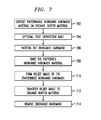
- FIG. 7 is a diagram illustrating an exemplary methodology for patterning an organic buffer material using an inorganic patternable hardmask according to an embodiment of the present invention.
- FIG. 1 is a cross-sectional diagram illustrating a starting structure for fabricating a carbon material-based (e.g., graphene or carbon nanotube-based) transistor.
- a substrate 102 is provided.
- Substrate 102 can be made of an electrically semiconducting material, an insulating material or a conductive material and/or substrate 102 can be a device or structure made of these materials or any combination thereof.
- carbon-based material 104 is then formed on substrate 102 .
- carbon-based material 104 consists of a layer or layers of graphene (as a single atomic layer of graphene, multi-layer graphene or a combination thereof) and/or carbon nanotubes (single wall carbon nanotubes, multiwall carbon nanotubes or a combination thereof).
- carbon-based material 104 may be formed on substrate 102 using any suitable deposition process, such as spin coating.
- suitable deposition process such as spin coating.
- carbon-based material 104 may be formed on substrate 102 using any suitable deposition process, such as chemical vapor deposition (CVD). Alternatively, a layer of graphene can be grown on substrate 102 . In that case, substrate 102 may contain silicon carbide (SiC).
- CVD chemical vapor deposition
- substrate 102 may contain silicon carbide (SiC).
- a portion of the carbon-based material will serve as a channel region of the transistor while other portions of the carbon-based material will serve as source and drain regions of the transistor.
- the transistors described herein will be top-gated devices.
- the portion of the carbon-based material under the top-gate will serve as a channel region of the transistor, while portions of the carbon-based material extending out from under the gate will serve as source and drain regions of the transistor.
- the top-gate will be separated from the (carbon-based material) channel region by a high-k gate dielectric.
- high-k gate dielectrics include, but are not limited to, one or more of hafnium dioxide, zirconium dioxide, aluminum oxide, titanium dioxide, hafnium silicate, zirconium silicate, and the like.
- an organic buffer layer will be used between the high-k gate dielectric and the channel region.
- the organic buffer layer and the high-k gate dielectric will together serve as a gate dielectric of the transistor (the organic buffer layer and the high-k gate dielectric are also collectively referred to herein as “a gate dielectric film stack”).
- FIG. 2 is a cross-sectional diagram illustrating an organic buffer material 202 having been deposited on carbon-based material 104 (on the graphene and/or carbon nanotube layer).
- organic buffer material 202 is deposited to a thickness of from about 1 nanometer (nm) to about 100 nm, e.g., from about 1 nm to about 10 nm.
- the organic buffer material 202 can be composed of small organic molecules, large organic molecules, biological molecules, such as a polymer, a copolymer or deoxyribonucleic acid (DNA), or a combination thereof.
- the organic buffer material is a patternable (either directly or indirectly) material.
- organic buffer material 202 includes a functional polymer, copolymer, or a blend including at least two of any combination of polymers and/or copolymers having one or more acid-sensitive imageable or direct imageable groups, and is formed from a composition that includes one of the polymers, copolymers or blends, a photoacid generator, a base additive and a solvent typically used in photoresists such as ethoxyethylpropionate (EEP), ⁇ -butyrolactone, propylene-glycol monomethylether alcohol, propylene-glycol monomethylether alcohol acetate, propyleneglycol monopropyl alcohol, propyleneglycol monopropyl alcohol acetate and ethyl lactate.
- EEP ethoxyethylpropionate
- the organic buffer material 202 can be configured as a negative tone patternable material.
- an additional cross-linking agent may be added to the composition.
- cross-linking agents include, but are not limited to, 2,6-bis(hydroxymethyl)-p-cresol, glycoluril compounds such as tetramethoxymethyl glycoluril, methylpropyltetramethoxymethyl glycoluril and methylphenyltetramethoxymethyl glycoluril, available under the POWDERLINK trademark from American Cyanamid Company.
- organic buffer material 202 is a copolymer of hydroxystyrene and a derivative of hydroxystyrene, for example, NFC, e.g., NFC 1400-3CP, produced by JSR Corp, Tokyo, Japan.
- NFC e.g., NFC 1400-3CP
- the pattern of the organic buffer layer is formed directly on the organic buffer material itself without the need for a hardmask layer and the related pattern transfer steps.
- an indirectly patternable organic buffer material the pattern is first formed on a patternable inorganic hardmask and then transferred to the organic buffer material to form the patterned organic buffer layer.
- the organic buffer material has the following attributes: 1) the organic buffer material adheres to and provides a thin and uniform coverage on the underlying active carbon-based material 104 (graphene and/or carbon nanotubes); 2) the organic buffer material serves as a nucleation and adhesion layer for the high-k gate dielectric deposited thereon; 3) as highlighted above, the organic buffer material serves as part of the gate dielectric film stack; and 4) the organic buffer material is compatible with the fabrication process of a carbon-based transistor with a high-k gate dielectric (i.e., the organic buffer material is stable (will not thermally decompose or de-adhere from the carbon-based material) during subsequent processing).
- organic moieties into the organic buffer material, such as aromatic hydrocarbon groups, that allow good wetting of the organic buffer material 202 on the underlying carbon-based material 104 .
- Good wetting of the organic buffer material 202 satisfies, for example, attribute 1, above.
- Suitable aromatic hydrocarbon groups include, but are not limited to, monoaromatic hydrocarbons or polyaromatic hydrocarbons.
- Exemplary aromatic hydrocarbons include benzene, biphenyl, bisphenyl, naphthalene, anthracene, benzo[a]pyrene, chrysene, coronene, corannulene, tetracene, pentacene, phenanthrene, pyrene, triphenylene, ovalene, fluoranthrenes, anthrones, benzophenones, thioxanthones, and the like.
- Anthracene derivatives such as those described in U.S. Pat. No.
- 9-anthracene methanol is a preferred aromatic hydrocarbon.
- Incorporating functional groups into the organic buffer material such as a hydroxyl group, an ether group, an ester group, a methyl group and/or hydrogen, permits good nucleation and adhesion for the high-k gate dielectric on the organic buffer material. These functional groups can be chemically attached (bonded) to the aromatic hydrocarbon or to the polymer, copolymer of the organic buffer material or both.
- the organic buffer material is configured to have both an organic moiety or moieties that facilitate wetting the underlying graphene/carbon nanotube material, and a functional group(s) that serve as a nucleation and adhesion site(s) for a high-k gate dielectric material.
- Organic buffer material 202 can be deposited on carbon-based material 104 using a range of film deposition methods such as spin coating, spray coating, dip coating and/or CVD.
- a post-deposition baking step may be employed to remove any residual solvent and/or to induce chemical reaction of the organic buffer material 202 .
- the post-deposition baking is carried out at a temperature of from about 50 degrees Celsius (° C.) to about 400° C., e.g., from about 100° C. to about 300° C., for a duration of from about 10 seconds to about 30 minutes, e.g., from about 30 seconds to about 5 minutes.
- the organic buffer material 202 can be cured after deposition to improve its thermal stability, adhesion, mechanical properties (such as hardness) and/or electrical properties (so as to serve as a better dielectric).
- the curing of the organic buffer material 202 may be performed using a thermal cure, an electron beam (e-beam) cure, an ultra-violet (UV) cure, an ion beam cure, a plasma cure, a microwave cure or a combination thereof.
- e-beam electron beam
- UV ultra-violet
- ion beam cure ion beam cure
- plasma cure a plasma cure
- microwave cure a combination thereof.
- the conditions for each of these curing processes are well known to those skilled in the art and any condition can be chosen as long as it improves the thermal stability, adhesion, mechanical properties and/or electrical properties of the organic buffer material.
- the patterning of the organic buffer material may be conducted using optical lithography at one of the following wavelengths: 365 nm, 248 nm, 193 nm, 13.4 nm and the like through a mask, e-beam lithography, nanoimprint, ink jet printing and the like.
- the patterning of the organic buffer material is carried out using optical lithography, the patterning can be carried out in a dry mode or an immersion mode.
- immersion lithography a high index liquid, i.e., a liquid having a refractive index that is greater than that of air (for example water), is placed between the material to be patterned and the optical lens used in the lithography.
- the immersion lithography procedure is known to those of skill in the art and thus is not described further herein.
- the patterning can be a single exposure patterning or multiple exposure patterning.
- the lithography target is exposed to the light source a single time.
- the lithography target is exposed to the light source multiple times with or without additional processing occurring in between each exposure.
- Multiple exposures patterning can be used to print finer features of the transistor.
- this exemplary embodiment employing a directly patternable organic buffer material the use of a hardmask as shown in FIGS. 2 and 3 does not apply and reference should next be made to FIG. 4 , described below.
- a patternable inorganic hardmask is employed. Namely, as shown in FIG. 2 , an inorganic hardmask 204 (a relief image, see below) is formed on organic buffer material 202 on an area over which a top-gate of the device will be formed (as described below).
- the inorganic hardmask 204 is used to pattern the underlying organic buffer material without the need of a separate photoresist as in conventional methods.
- the advantages of this novel patterning scheme is that it is more cost-effective than conventional processes and provides a self-aligned, high-speed graphene or carbon nanotube-based transistor with a high-k gate dielectric.
- inorganic hardmask 204 is deposited on the organic buffer material 202 and then patterned to form inorganic hardmask 204 .
- the process for patterning inorganic hardmask 204 is the same as that for patterning a patternable low-k material as described, for example, in U.S. Pat. No. 7,041,748 issued to Lin et al., entitled “Patternable Low Dielectric Constant Materials and Their Use in ULSI Interconnection” (hereinafter “U.S. Pat. No. 7,041,748”), U.S. Pat. No.
- Patent Application Publication Number 2008/0286467 U.S. Patent Application Publication Number 2009/0233226 filed by Allen et al., entitled “Photopatternable Dielectric Materials for BEOL Applications and Methods for Use”
- U.S. Patent Application Publication Number 2009/0233226 U.S. Patent Application Publication Number 2009/0233226
- U.S. Patent Application Publication Number 2009/0291389 filed by Allen et al., entitled “Photopatternable Dielectric Materials for BEOL Applications and Methods for Use”
- U.S. Patent Application Publication Number 2009/0291389 The contents of each of the foregoing patents and patent applications are incorporated by reference herein.
- the patternable inorganic hardmask material can be formed on organic buffer material 202 using a conventional deposition process, such as spin coating, dip coating, brush coating and ink-jet printing.
- a post-deposition baking may be employed to remove unwanted components, such as solvent.
- the baking step is conducted at a temperature of from about 40° C. to about 200° C., e.g., from about 60° C. to about 140° C., for a duration of, for example, from about 10 seconds to about 600 seconds.
- the thickness of the deposited patternable inorganic hardmask material may vary depending on the requirements of the transistor and the techniques used to form the transistor (i.e., the inorganic hardmask needs to have a sufficient thickness to transfer an image from itself to the organic buffer material) as well as the material make-up of the layer.
- the patternable inorganic hardmask material is deposited to a thickness from about 1 nm to about 50,000 nm, e.g., from about 10 nm to about 500 nm.
- the patternable inorganic hardmask material may be made up of a functionalized polymer, copolymer, or a blend including at least two of any combination of polymers and/or copolymers having one or more acid-sensitive imageable groups.
- the blends of polymers and/or copolymers include at least two of any combination of polymers and/or copolymers.
- the patternable inorganic hardmask material is formed from a composition that includes one of the polymers, copolymers or blends, a photoacid generator, a base additive and a solvent commonly used in photoresists such as ethoxyethylpropionate (EEP), ⁇ -butyrolactone, propylene-glycol monomethylether alcohol, propylene-glycol monomethylether alcohol acetate, propylene glycol monopropyl alcohol, propylene glycol monopropyl alcohol acetate and ethyl lactate.
- the patternable inorganic hardmask material can be configured as a negative tone patternable material. In that instance, an additional cross-linking agent may be added to the above-described composition.
- cross-linking agents include, but are not limited to, 2,6-bis(hydroxymethyl)-p-cresol, glycoluril compounds such as tetramethoxymethyl glycoluril, methylpropyltetramethoxymethyl glycoluril, and methylphenyltetramethoxymethyl glycoluril, available under the POWDERLINK trademark from American Cyanamid Company.
- the patternable inorganic hardmask material includes a polymer, a copolymer, or a blend including at least two of any combination of polymers and/or copolymers, wherein the polymers include one monomer and the copolymers include at least two monomers and wherein the monomers of the polymers and the monomers of the copolymers are selected from a siloxane, silane, carbosilane, oxycarbosilane, silsesquioxane, alkyltrialkoxysilane, tetra-alkoxysilane, unsaturated alkyl substituted silsesquioxane, unsaturated alkyl substituted siloxane, unsaturated alkyl substituted silane, an unsaturated alkyl substituted carbosilane, unsaturated alkyl substituted oxycarbosilane, carbosilane substituted silsesquioxane, carbosilane substituted siloxane, carbosilane substituted
- the patternable inorganic hardmask material includes a photo/acid-sensitive polymer of one monomer or a copolymer of at least two monomers selected from siloxane, silane, carbosilane, oxycarbosilane, organosilicates, silsesquioxanes and the like.
- the inorganic hardmask may also include a polymer of one monomer or a copolymer of at least two monomers selected from alkyltrialkoxysilane, tetra-alkoxysilane, unsaturated alkyl (such as vinyl) substituted silsesquioxane, unsaturated alkyl substituted siloxane, unsaturated alkyl substituted silane, an unsaturated alkyl substituted carbosilane, unsaturated alkyl substituted oxycarbosilane, carbosilane substituted silsesquioxane, carbosilane substituted siloxane, carbosilane substituted silane, carbosilane substituted carbosilane, carbosilane substituted oxycarbosilane, oxycarbosilane substituted silsesquioxane, oxycarbosilane substituted siloxane, oxycarbosilane substituted siloxane, oxycarb
- the inorganic hardmask may include a blend including at least two of any combination of polymers and/or copolymers, wherein the polymers include one monomer and the copolymers include at least two monomers and wherein the monomers of the polymers and the monomers of the copolymers are selected from a siloxane, silane, carbosilane, oxycarbosilane, silsesquioxane, alkyltrialkoxysilane, tetra-alkoxysilane, unsaturated alkyl substituted silsesquioxane, unsaturated alkyl substituted siloxane, unsaturated alkyl substituted silane, an unsaturated alkyl substituted carbosilane, unsaturated alkyl substituted oxycarbosilane, carbosilane substituted silsesquioxane, carbosilane substituted siloxane, carbosilane substituted silane, carbosilane substituted carbosilane
- patternable inorganic hardmask materials that may be used in conjunction with the present techniques are the patternable low-k materials described, for example, in U.S. Pat. No. 7,041,748, U.S. Pat. No. 7,056,840, U.S. Pat. No. 6,087,064, U.S. Patent Application Publication Number 2008/0286467, U.S. Patent Application Publication Number 2009/0233226 and U.S. Patent Application Publication Number 2009/0291389.
- a pattern-wise exposure of the patternable inorganic hardmask is performed. Specifically, the inorganic hardmask material is exposed to radiation and developed with a developer to form patterns. This patterning process on the inorganic hardmask may be carried out using optical lithography, electron-beam lithography or other patterning techniques known in the art.
- a post-exposure baking of the inorganic hardmask material is then conducted to remove unwanted components, such as solvent.
- the post-exposure baking of the inorganic hardmask material is carried out at a temperature of from about 50° C. to about 400° C., e.g., from about 100° C. to about 300° C., for a duration of from about 10 seconds to about 30 minutes, e.g., from about 30 seconds to about 5 minutes.
- a relief image 204 is then formed from the patterns by developing the inorganic hardmask with an aqueous base solution, such as a tetramethyl aminohydroxide (TMAH) solution.
- a aqueous base solution such as a tetramethyl aminohydroxide (TMAH) solution.
- TMAH tetramethyl aminohydroxide
- the relief image 204 corresponds to the desired footprint and location of the gate dielectric, i.e., of the organic buffer material on top of the carbon-based material and between the carbon-based material and the high-k gate dielectric.
- the relief image 204 is then transferred to the organic buffer material 202 .
- FIG. 3 is a cross-sectional diagram illustrating inorganic hardmask relief image 204 having been used to pattern organic buffer material 202 , resulting in patterned organic buffer layer 202 a , without any detrimental effect on the underlying carbon-based material (which is achievable using the patterning procedures described below).
- Patterned organic buffer layer 202 a is present over a portion of carbon-based material 104 that will serve as a channel region of the transistor.
- the organic buffer layer is patterned using either a wet or a dry etching process without adversely affecting the desirable (e.g., electrical) properties of the underlying carbon-based material.
- the organic buffer layer is patterned with a wet method by using a solvent that is capable of removing the exposed portions of the organic buffer material.
- suitable solvents include, but are not limited to, an organic hydrocarbon, an alcohol, ether and/or an ester.
- some suitable solvents include ethoxyethylpropionate (EEP), ⁇ -butyrolactone, propylene-glycol monomethylether alcohol, propylene-glycol monomethylether alcohol acetate, propylene glycol monopropyl alcohol, propylene glycol monopropyl alcohol acetate and ethyl lactate. Combinations of these aforementioned solvents may also be used.
- the solvent removal of the exposed portion of the organic buffer material may be carried out in a container or on the lithography track.
- the process can be carried out at temperatures ranging from room temperature to elevated temperatures of from about 23° C. to about 150° C., for a duration of from about 1 second to about 30 minutes, e.g., from about 10 seconds to about 5 minutes.
- FIG. 4 is a cross-sectional diagram illustrating inorganic hardmask relief image 204 having been removed.
- Inorganic hardmask relief image 204 may be removed by a wet etch method with a solvent or a solution. This wet removal method does not affect the physical properties of the graphene or carbon nanotubes and retains the pattern integrity of the patterned organic buffer layer.
- Typical examples of the solvent or solutions are an acid, a base, or an aqueous solution or a combination thereof.
- the acid include dilute hydrofluoric (HF) acid, sulfuric acid and the like.
- Examples of the base are tetramethyl aminohydroxide (TMAH), potassium hydroxide (KOH) and the like.
- the hardmask removal process can be carried out at room temperature, or at an elevated temperature at which the organic buffer layer remains intact, typically below about 250° C.
- the hardmask removal process involves soaking the device in the appropriate solvent or solution for a duration of from about 1 second to about 30 minutes, for example, for a duration of from about 10 seconds to about 5 minutes, e.g., for a duration of from about 30 seconds to about 2 minutes. Agitation (for example using an ultrasonic agitator) during the soak may be employed to assist with the hardmask removal.
- the hardmask removal process may be carried out in a series of steps, for example, involving a soak (according to the time/temperature parameters provided above) in an acid, followed by a rinse and then a soak (according to the time/temperature parameters provided above) in a base.
- a soak accordinging to the time/temperature parameters provided above
- a rinse according to the time/temperature parameters provided above
- a soak according to the time/temperature parameters provided above
- FIG. 5 is a cross-sectional diagram illustrating a conformal high-k gate dielectric layer 502 having been selectively deposited over patterned organic buffer layer 202 a .
- the conformal high-k gate dielectric layer is selectively deposited over patterned organic buffer layer 202 a using atomic layer deposition (ALD), CVD or physical vapor deposition (PVD).
- ALD atomic layer deposition
- CVD chemical vapor deposition
- PVD physical vapor deposition
- High-k materials and their corresponding chemical precursors that can be used for gate dielectric ALD include, but are not limited to, aluminum oxide (Al 2 O 3 ) (water and Trimethylaluminum precursors) and hafnium dioxide (HfO 2 ) (water and Tetrakis(dimethylamido)hafnium precursors.
- precursors that can be used for ALD and/or CVD include, but are not limited to, Aluminum sec-butoxide, Aluminum tribromide, Aluminum trichloride, Diethylaluminum ethoxide, Tris(ethylmethylamido)aluminum, Triethylaluminum, Triisobutylaluminum, Tris(diethylamido)aluminum, Tris(ethylmethylamido)aluminum, Hafnium(IV) chloride, Hafnium(IV) tert-butoxide, Tetrakis(diethylamido)hafnium(IV), Tetrakis(dimethylamido)hafnium(IV), Tetrakis(ethylmethylamido)hafnium(IV), Ozone, and Oxygen.
- high-k gate dielectrics such as Al 2 O 3 and HfO 2 can be deposited from their bulk, solid-state sources as is known in
- FIG. 6 is a cross-sectional diagram illustrating source and drain contacts 602 and 604 and top-gate contact 606 , labeled “S,” “D” and “TG,” respectively, having been formed.
- Source and drain contacts 602 and 604 are formed on portions of carbon-based material 104 that will serve as source and drain regions of the transistor and are connected to the portion of the carbon-based material 104 that will serve as the channel region of the transistor (i.e., the portion underneath the gate dielectric film stack).
- Top-gate contact 606 is formed on the high-k gate dielectric layer 502 .
- source and drain contacts 602 and 604 and top-gate contact 606 are formed by thermal evaporation using a metal(s), such as one or more of palladium (Pd), titanium (Ti), gold (Au), tungsten (W), aluminum (Al), nickel (Ni) and platinum (Pt).
- a metal(s) such as one or more of palladium (Pd), titanium (Ti), gold (Au), tungsten (W), aluminum (Al), nickel (Ni) and platinum (Pt).
- FIG. 7 is a diagram summarizing the above-described exemplary novel methodology for patterning an organic buffer material using an inorganic patternable hardmask.
- the present process does not involve the use of a separate photoresist as in conventional methods making it more efficient and more cost-effective.
- the patternable inorganic hardmask material is deposited on the organic buffer material. Suitable patternable inorganic hardmask materials and deposition processes were described in detail above.
- an optional post-deposition baking of the inorganic hardmask material is performed. The parameters for this optional baking step were provided above.
- step 706 a pattern-wise exposing of the inorganic hardmask material is performed. As described above, this step of patterning the inorganic hardmask may be carried out using optical lithography, electron-beam lithography or other patterning techniques known in the art.
- step 708 a baking of the patterned inorganic hardmask material is then performed. This baking serves to remove unwanted components, such as solvent. The parameters for this baking step were described in detail above.
- step 710 a relief image of the (patterned) inorganic hardmask is formed using a developer, such as a TMAH solution.
- step 712 the relief image is transferred into the organic buffer material. As described above, this patterning of the organic buffer material can be performed using either a wet or a dry etching process. Finally in step 714 , the inorganic hardmask relief image is removed to expose the surface and sidewalls of the now-patterned organic buffer layer.
Abstract
Description
Claims (17)
Priority Applications (1)
| Application Number | Priority Date | Filing Date | Title |
|---|---|---|---|
| US13/007,644 US8617941B2 (en) | 2011-01-16 | 2011-01-16 | High-speed graphene transistor and method of fabrication by patternable hard mask materials |
Applications Claiming Priority (1)
| Application Number | Priority Date | Filing Date | Title |
|---|---|---|---|
| US13/007,644 US8617941B2 (en) | 2011-01-16 | 2011-01-16 | High-speed graphene transistor and method of fabrication by patternable hard mask materials |
Publications (2)
| Publication Number | Publication Date |
|---|---|
| US20120181506A1 US20120181506A1 (en) | 2012-07-19 |
| US8617941B2 true US8617941B2 (en) | 2013-12-31 |
Family
ID=46490094
Family Applications (1)
| Application Number | Title | Priority Date | Filing Date |
|---|---|---|---|
| US13/007,644 Active 2031-10-12 US8617941B2 (en) | 2011-01-16 | 2011-01-16 | High-speed graphene transistor and method of fabrication by patternable hard mask materials |
Country Status (1)
| Country | Link |
|---|---|
| US (1) | US8617941B2 (en) |
Cited By (11)
| Publication number | Priority date | Publication date | Assignee | Title |
|---|---|---|---|---|
| US20160276453A1 (en) * | 2013-11-11 | 2016-09-22 | National Institute For Materials Science | Electrical conduction element, electronic device, and method for operating electrical conduction element |
| US9618474B2 (en) | 2014-12-18 | 2017-04-11 | Edico Genome, Inc. | Graphene FET devices, systems, and methods of using the same for sequencing nucleic acids |
| US9679975B2 (en) | 2014-11-17 | 2017-06-13 | Samsung Electronics Co., Ltd. | Semiconductor devices including field effect transistors and methods of forming the same |
| US9859394B2 (en) | 2014-12-18 | 2018-01-02 | Agilome, Inc. | Graphene FET devices, systems, and methods of using the same for sequencing nucleic acids |
| US9857328B2 (en) | 2014-12-18 | 2018-01-02 | Agilome, Inc. | Chemically-sensitive field effect transistors, systems and methods for manufacturing and using the same |
| US20180019282A1 (en) * | 2016-07-14 | 2018-01-18 | International Business Machines Corporation | Carbon nanotube transistor and logic with end-bonded metal contacts |
| US20180019420A1 (en) * | 2016-07-14 | 2018-01-18 | International Business Machines Corporation | N-type end-bonded metal contacts for carbon nanotube transistors |
| US10006910B2 (en) | 2014-12-18 | 2018-06-26 | Agilome, Inc. | Chemically-sensitive field effect transistors, systems, and methods for manufacturing and using the same |
| US10020300B2 (en) | 2014-12-18 | 2018-07-10 | Agilome, Inc. | Graphene FET devices, systems, and methods of using the same for sequencing nucleic acids |
| US10429342B2 (en) | 2014-12-18 | 2019-10-01 | Edico Genome Corporation | Chemically-sensitive field effect transistor |
| US10811539B2 (en) | 2016-05-16 | 2020-10-20 | Nanomedical Diagnostics, Inc. | Graphene FET devices, systems, and methods of using the same for sequencing nucleic acids |
Families Citing this family (17)
| Publication number | Priority date | Publication date | Assignee | Title |
|---|---|---|---|---|
| US8748871B2 (en) * | 2011-01-19 | 2014-06-10 | International Business Machines Corporation | Graphene devices and semiconductor field effect transistors in 3D hybrid integrated circuits |
| US8969154B2 (en) * | 2011-08-23 | 2015-03-03 | Micron Technology, Inc. | Methods for fabricating semiconductor device structures and arrays of vertical transistor devices |
| US8569121B2 (en) | 2011-11-01 | 2013-10-29 | International Business Machines Corporation | Graphene and nanotube/nanowire transistor with a self-aligned gate structure on transparent substrates and method of making same |
| US9006087B2 (en) | 2013-02-07 | 2015-04-14 | International Business Machines Corporation | Diode structure and method for wire-last nanomesh technologies |
| KR102059131B1 (en) * | 2013-04-05 | 2019-12-24 | 삼성전자주식회사 | Graphene device, and method of fabricating the same |
| CN103700592B (en) * | 2013-11-29 | 2016-01-27 | 中国电子科技集团公司第五十五研究所 | The manufacture method of the two-dimensional material field-effect transistor of grid structure is buried based on autoregistration |
| CN103915327B (en) * | 2014-03-05 | 2016-04-20 | 复旦大学 | Utilize island graphene film on Graphene, grow the method for high K dielectric |
| CN103915328B (en) * | 2014-03-05 | 2017-01-04 | 复旦大学 | Utilize the charged method growing high K dielectric on Graphene of Graphene |
| TWI675907B (en) * | 2015-01-21 | 2019-11-01 | 日商Jsr股份有限公司 | Solid imaging device |
| US20160264421A1 (en) * | 2015-03-09 | 2016-09-15 | International Business Machines Corporation | Multilayer graphene structure reinforced with polyaromatic interstitial layers |
| US9882008B2 (en) | 2015-11-05 | 2018-01-30 | Texas Instruments Incorporated | Graphene FET with graphitic interface layer at contacts |
| US11222959B1 (en) * | 2016-05-20 | 2022-01-11 | Hrl Laboratories, Llc | Metal oxide semiconductor field effect transistor and method of manufacturing same |
| US11315961B2 (en) | 2017-03-17 | 2022-04-26 | Ricoh Company, Ltd. | Field-effect transistor, method for producing same, display element, display device, and system |
| CN108054209B (en) * | 2017-12-14 | 2020-08-11 | 北京华碳科技有限责任公司 | Field-effect transistor, method of manufacturing field-effect transistor, and electronic device |
| CN109686667A (en) * | 2019-01-25 | 2019-04-26 | 泰科天润半导体科技(北京)有限公司 | A kind of SiC base MOS device and its preparation method and application |
| CN111693589A (en) * | 2020-06-02 | 2020-09-22 | 中国科学院微电子研究所 | Method for manufacturing biosensor, and application of biosensor |
| US11588030B2 (en) * | 2020-09-29 | 2023-02-21 | Taiwan Semiconductor Manufacturing Co., Ltd. | Integrated circuit structure and manufacturing method thereof |
Citations (14)
| Publication number | Priority date | Publication date | Assignee | Title |
|---|---|---|---|---|
| US4371605A (en) | 1980-12-09 | 1983-02-01 | E. I. Du Pont De Nemours And Company | Photopolymerizable compositions containing N-hydroxyamide and N-hydroxyimide sulfonates |
| US6087064A (en) | 1998-09-03 | 2000-07-11 | International Business Machines Corporation | Silsesquioxane polymers, method of synthesis, photoresist composition, and multilayer lithographic method |
| US7041748B2 (en) | 2003-01-08 | 2006-05-09 | International Business Machines Corporation | Patternable low dielectric constant materials and their use in ULSI interconnection |
| US7056840B2 (en) | 2003-09-30 | 2006-06-06 | International Business Machines Corp. | Direct photo-patterning of nanoporous organosilicates, and method of use |
| US20080286467A1 (en) | 2007-05-18 | 2008-11-20 | Allen Robert D | Method of use for photopatternable dielectric materials for beol applications |
| US20090181502A1 (en) | 2008-01-16 | 2009-07-16 | Texas Instruments Incorporated | Method for fabricating graphene transistors on a silicon or soi substrate |
| US20090233226A1 (en) | 2008-03-13 | 2009-09-17 | International Business Machines Corporation | Photopatternable dielectric materials for beol applications and methods for use |
| US20090237580A1 (en) * | 2008-03-20 | 2009-09-24 | Tpo Displays Corp. | System for display images and fabrication method thereof |
| US20090291389A1 (en) | 2008-05-23 | 2009-11-26 | International Business Machines Corporation | Photopatternable dielectric materials for beol applications and methods for use |
| US20100213435A1 (en) * | 2009-02-24 | 2010-08-26 | Shosuke Fujii | Switching device and nonvolatile memory device |
| US20110017979A1 (en) * | 2009-07-21 | 2011-01-27 | The Trustees Of Columbia University In The City Of New York | High-performance gate oxides such as for graphene field-effect transistors or carbon nanotubes |
| US20110031490A1 (en) * | 2009-08-05 | 2011-02-10 | Sony Corporation | Thin film transistor |
| US20120056161A1 (en) * | 2010-09-07 | 2012-03-08 | International Business Machines Corporation | Graphene transistor with a self-aligned gate |
| US20120205668A1 (en) * | 2005-11-01 | 2012-08-16 | Atsuo Watanabe | Switching semiconductor devices and fabrication process |
-
2011
- 2011-01-16 US US13/007,644 patent/US8617941B2/en active Active
Patent Citations (14)
| Publication number | Priority date | Publication date | Assignee | Title |
|---|---|---|---|---|
| US4371605A (en) | 1980-12-09 | 1983-02-01 | E. I. Du Pont De Nemours And Company | Photopolymerizable compositions containing N-hydroxyamide and N-hydroxyimide sulfonates |
| US6087064A (en) | 1998-09-03 | 2000-07-11 | International Business Machines Corporation | Silsesquioxane polymers, method of synthesis, photoresist composition, and multilayer lithographic method |
| US7041748B2 (en) | 2003-01-08 | 2006-05-09 | International Business Machines Corporation | Patternable low dielectric constant materials and their use in ULSI interconnection |
| US7056840B2 (en) | 2003-09-30 | 2006-06-06 | International Business Machines Corp. | Direct photo-patterning of nanoporous organosilicates, and method of use |
| US20120205668A1 (en) * | 2005-11-01 | 2012-08-16 | Atsuo Watanabe | Switching semiconductor devices and fabrication process |
| US20080286467A1 (en) | 2007-05-18 | 2008-11-20 | Allen Robert D | Method of use for photopatternable dielectric materials for beol applications |
| US20090181502A1 (en) | 2008-01-16 | 2009-07-16 | Texas Instruments Incorporated | Method for fabricating graphene transistors on a silicon or soi substrate |
| US20090233226A1 (en) | 2008-03-13 | 2009-09-17 | International Business Machines Corporation | Photopatternable dielectric materials for beol applications and methods for use |
| US20090237580A1 (en) * | 2008-03-20 | 2009-09-24 | Tpo Displays Corp. | System for display images and fabrication method thereof |
| US20090291389A1 (en) | 2008-05-23 | 2009-11-26 | International Business Machines Corporation | Photopatternable dielectric materials for beol applications and methods for use |
| US20100213435A1 (en) * | 2009-02-24 | 2010-08-26 | Shosuke Fujii | Switching device and nonvolatile memory device |
| US20110017979A1 (en) * | 2009-07-21 | 2011-01-27 | The Trustees Of Columbia University In The City Of New York | High-performance gate oxides such as for graphene field-effect transistors or carbon nanotubes |
| US20110031490A1 (en) * | 2009-08-05 | 2011-02-10 | Sony Corporation | Thin film transistor |
| US20120056161A1 (en) * | 2010-09-07 | 2012-03-08 | International Business Machines Corporation | Graphene transistor with a self-aligned gate |
Non-Patent Citations (1)
| Title |
|---|
| Farmer et al., "Utilization of a Buffered Dielectric to Achieve High Field-Effect Carrier Mobility in Graphene Transistors," Nano Letters, vol. 9, No. 12, pp. 4474-4478 (2009). |
Cited By (21)
| Publication number | Priority date | Publication date | Assignee | Title |
|---|---|---|---|---|
| US20160276453A1 (en) * | 2013-11-11 | 2016-09-22 | National Institute For Materials Science | Electrical conduction element, electronic device, and method for operating electrical conduction element |
| US9627499B2 (en) * | 2013-11-11 | 2017-04-18 | National Institute For Materials Science | Electrical conduction element, electronic device, and method for operating electrical conduction element |
| US10868125B2 (en) | 2014-11-17 | 2020-12-15 | Samsung Electronics Co., Ltd. | Semiconductor devices including field effect transistors and methods of forming the same |
| US9679975B2 (en) | 2014-11-17 | 2017-06-13 | Samsung Electronics Co., Ltd. | Semiconductor devices including field effect transistors and methods of forming the same |
| US10418448B2 (en) | 2014-11-17 | 2019-09-17 | Samsung Electronics Co., Ltd. | Semiconductor devices including field effect transistors and methods of forming the same |
| US9857328B2 (en) | 2014-12-18 | 2018-01-02 | Agilome, Inc. | Chemically-sensitive field effect transistors, systems and methods for manufacturing and using the same |
| US10429381B2 (en) | 2014-12-18 | 2019-10-01 | Agilome, Inc. | Chemically-sensitive field effect transistors, systems, and methods for manufacturing and using the same |
| US9618474B2 (en) | 2014-12-18 | 2017-04-11 | Edico Genome, Inc. | Graphene FET devices, systems, and methods of using the same for sequencing nucleic acids |
| US10006910B2 (en) | 2014-12-18 | 2018-06-26 | Agilome, Inc. | Chemically-sensitive field effect transistors, systems, and methods for manufacturing and using the same |
| US10020300B2 (en) | 2014-12-18 | 2018-07-10 | Agilome, Inc. | Graphene FET devices, systems, and methods of using the same for sequencing nucleic acids |
| US9859394B2 (en) | 2014-12-18 | 2018-01-02 | Agilome, Inc. | Graphene FET devices, systems, and methods of using the same for sequencing nucleic acids |
| US10429342B2 (en) | 2014-12-18 | 2019-10-01 | Edico Genome Corporation | Chemically-sensitive field effect transistor |
| US10607989B2 (en) | 2014-12-18 | 2020-03-31 | Nanomedical Diagnostics, Inc. | Graphene FET devices, systems, and methods of using the same for sequencing nucleic acids |
| US10494670B2 (en) | 2014-12-18 | 2019-12-03 | Agilome, Inc. | Graphene FET devices, systems, and methods of using the same for sequencing nucleic acids |
| US10811539B2 (en) | 2016-05-16 | 2020-10-20 | Nanomedical Diagnostics, Inc. | Graphene FET devices, systems, and methods of using the same for sequencing nucleic acids |
| US20180019282A1 (en) * | 2016-07-14 | 2018-01-18 | International Business Machines Corporation | Carbon nanotube transistor and logic with end-bonded metal contacts |
| US10665799B2 (en) * | 2016-07-14 | 2020-05-26 | International Business Machines Corporation | N-type end-bonded metal contacts for carbon nanotube transistors |
| US10665798B2 (en) * | 2016-07-14 | 2020-05-26 | International Business Machines Corporation | Carbon nanotube transistor and logic with end-bonded metal contacts |
| US20180019420A1 (en) * | 2016-07-14 | 2018-01-18 | International Business Machines Corporation | N-type end-bonded metal contacts for carbon nanotube transistors |
| US11121335B2 (en) | 2016-07-14 | 2021-09-14 | International Business Machines Corporation | Carbon nanotube transistor and logic with end-bonded metal contacts |
| US11545641B2 (en) | 2016-07-14 | 2023-01-03 | International Business Machines Corporation | N-type end-bonded metal contacts for carbon nanotube transistors |
Also Published As
| Publication number | Publication date |
|---|---|
| US20120181506A1 (en) | 2012-07-19 |
Similar Documents
| Publication | Publication Date | Title |
|---|---|---|
| US8617941B2 (en) | High-speed graphene transistor and method of fabrication by patternable hard mask materials | |
| TWI496242B (en) | Patternable low-k dielectric interconnect structure with a graded cap layer and method of fabrication | |
| US8637395B2 (en) | Methods for photo-patternable low-k (PPLK) integration with curing after pattern transfer | |
| US20120248416A1 (en) | High Performance Field-Effect Transistors | |
| US9190493B2 (en) | Photopatternable materials and related electronic devices and methods | |
| US7226804B2 (en) | Method for forming pattern of organic insulating film | |
| US9087753B2 (en) | Printed transistor and fabrication method | |
| KR20150131074A (en) | Field effect transistor | |
| US7741635B2 (en) | Composition for organic polymer gate insulating layer and organic thin film transistor using the same | |
| WO2023115654A1 (en) | Indium tin oxide vertical gate-all-around field effect transistor and preparation method therefor | |
| US9117914B1 (en) | VTFT with polymer core | |
| US9123815B1 (en) | VTFTs including offset electrodes | |
| US9147770B1 (en) | VTFT with extended electrode | |
| US9214560B2 (en) | VTFT including overlapping electrodes | |
| US20150255583A1 (en) | Fabricating vtft with polymer core | |
| JP6606564B2 (en) | Method for manufacturing image sensor device | |
| US9198283B2 (en) | Vertically spaced electrode structure | |
| US9129993B1 (en) | Forming a VTFT using printing | |
| US9093470B1 (en) | VTFT formation using capillary action | |
| TWI469224B (en) | Organic thin film transistor and fabricating the same | |
| US20150255625A1 (en) | Offset independently operable vtft electrodes | |
| US8652964B2 (en) | Method and apparatus for the formation of an electronic device | |
| US11417849B2 (en) | Fabrication of corrugated gate dielectric structures using atomic layer etching | |
| TWI833204B (en) | Method for forming photoresist | |
| US20230154750A1 (en) | Photoresist and Method |
Legal Events
| Date | Code | Title | Description |
|---|---|---|---|
| AS | Assignment |
Owner name: INTERNATIONAL BUSINESS MACHINES CORPORATION, NEW Y Free format text: ASSIGNMENT OF ASSIGNORS INTEREST;ASSIGNORS:FARMER, DAMON BROOKS;LIN, QINGHUANG;LIN, YU-MING;REEL/FRAME:025646/0379 Effective date: 20110113 |
|
| STCF | Information on status: patent grant |
Free format text: PATENTED CASE |
|
| AS | Assignment |
Owner name: GLOBALFOUNDRIES U.S. 2 LLC, NEW YORK Free format text: ASSIGNMENT OF ASSIGNORS INTEREST;ASSIGNOR:INTERNATIONAL BUSINESS MACHINES CORPORATION;REEL/FRAME:036550/0001 Effective date: 20150629 |
|
| AS | Assignment |
Owner name: GLOBALFOUNDRIES INC., CAYMAN ISLANDS Free format text: ASSIGNMENT OF ASSIGNORS INTEREST;ASSIGNORS:GLOBALFOUNDRIES U.S. 2 LLC;GLOBALFOUNDRIES U.S. INC.;REEL/FRAME:036779/0001 Effective date: 20150910 |
|
| FPAY | Fee payment |
Year of fee payment: 4 |
|
| AS | Assignment |
Owner name: WILMINGTON TRUST, NATIONAL ASSOCIATION, DELAWARE Free format text: SECURITY AGREEMENT;ASSIGNOR:GLOBALFOUNDRIES INC.;REEL/FRAME:049490/0001 Effective date: 20181127 |
|
| AS | Assignment |
Owner name: GLOBALFOUNDRIES U.S. INC., CALIFORNIA Free format text: ASSIGNMENT OF ASSIGNORS INTEREST;ASSIGNOR:GLOBALFOUNDRIES INC.;REEL/FRAME:054633/0001 Effective date: 20201022 |
|
| AS | Assignment |
Owner name: GLOBALFOUNDRIES INC., CAYMAN ISLANDS Free format text: RELEASE BY SECURED PARTY;ASSIGNOR:WILMINGTON TRUST, NATIONAL ASSOCIATION;REEL/FRAME:054636/0001 Effective date: 20201117 |
|
| AS | Assignment |
Owner name: GLOBALFOUNDRIES U.S. INC., NEW YORK Free format text: RELEASE BY SECURED PARTY;ASSIGNOR:WILMINGTON TRUST, NATIONAL ASSOCIATION;REEL/FRAME:056987/0001 Effective date: 20201117 |
|
| MAFP | Maintenance fee payment |
Free format text: PAYMENT OF MAINTENANCE FEE, 8TH YEAR, LARGE ENTITY (ORIGINAL EVENT CODE: M1552); ENTITY STATUS OF PATENT OWNER: LARGE ENTITY Year of fee payment: 8 |