US8610336B1 - Microelectromechanical resonators having resistive heating elements therein configured to provide frequency tuning through convective heating of resonator bodies - Google Patents
Microelectromechanical resonators having resistive heating elements therein configured to provide frequency tuning through convective heating of resonator bodies Download PDFInfo
- Publication number
- US8610336B1 US8610336B1 US13/250,560 US201113250560A US8610336B1 US 8610336 B1 US8610336 B1 US 8610336B1 US 201113250560 A US201113250560 A US 201113250560A US 8610336 B1 US8610336 B1 US 8610336B1
- Authority
- US
- United States
- Prior art keywords
- resonator
- resistive heating
- microelectromechanical
- substrate
- heating element
- Prior art date
- Legal status (The legal status is an assumption and is not a legal conclusion. Google has not performed a legal analysis and makes no representation as to the accuracy of the status listed.)
- Expired - Fee Related, expires
Links
- 238000010438 heat treatment Methods 0.000 title claims abstract description 72
- 239000000758 substrate Substances 0.000 claims abstract description 50
- 238000002955 isolation Methods 0.000 claims description 9
- 239000000463 material Substances 0.000 description 32
- VYPSYNLAJGMNEJ-UHFFFAOYSA-N silicon dioxide Inorganic materials O=[Si]=O VYPSYNLAJGMNEJ-UHFFFAOYSA-N 0.000 description 10
- 238000000034 method Methods 0.000 description 9
- 229910052710 silicon Inorganic materials 0.000 description 9
- 239000010703 silicon Substances 0.000 description 9
- XUIMIQQOPSSXEZ-UHFFFAOYSA-N Silicon Chemical compound [Si] XUIMIQQOPSSXEZ-UHFFFAOYSA-N 0.000 description 8
- 239000004065 semiconductor Substances 0.000 description 7
- 239000002131 composite material Substances 0.000 description 6
- 235000012239 silicon dioxide Nutrition 0.000 description 6
- 239000010409 thin film Substances 0.000 description 6
- 230000015572 biosynthetic process Effects 0.000 description 5
- 230000008878 coupling Effects 0.000 description 4
- 238000010168 coupling process Methods 0.000 description 4
- 238000005859 coupling reaction Methods 0.000 description 4
- 238000003780 insertion Methods 0.000 description 4
- 230000037431 insertion Effects 0.000 description 4
- 239000012212 insulator Substances 0.000 description 4
- 238000004519 manufacturing process Methods 0.000 description 4
- 239000010453 quartz Substances 0.000 description 4
- IJGRMHOSHXDMSA-UHFFFAOYSA-N Atomic nitrogen Chemical compound N#N IJGRMHOSHXDMSA-UHFFFAOYSA-N 0.000 description 3
- 229910001873 dinitrogen Inorganic materials 0.000 description 3
- 230000010354 integration Effects 0.000 description 3
- 238000012545 processing Methods 0.000 description 3
- 239000000377 silicon dioxide Substances 0.000 description 3
- 230000008021 deposition Effects 0.000 description 2
- 150000004767 nitrides Chemical class 0.000 description 2
- 229910021420 polycrystalline silicon Inorganic materials 0.000 description 2
- 229920005591 polysilicon Polymers 0.000 description 2
- WFKWXMTUELFFGS-UHFFFAOYSA-N tungsten Chemical compound [W] WFKWXMTUELFFGS-UHFFFAOYSA-N 0.000 description 2
- 229910052721 tungsten Inorganic materials 0.000 description 2
- 239000010937 tungsten Substances 0.000 description 2
- 101100352919 Caenorhabditis elegans ppm-2 gene Proteins 0.000 description 1
- ZOKXTWBITQBERF-UHFFFAOYSA-N Molybdenum Chemical compound [Mo] ZOKXTWBITQBERF-UHFFFAOYSA-N 0.000 description 1
- 229910052681 coesite Inorganic materials 0.000 description 1
- 238000004891 communication Methods 0.000 description 1
- 229910052906 cristobalite Inorganic materials 0.000 description 1
- 239000013078 crystal Substances 0.000 description 1
- 238000011161 development Methods 0.000 description 1
- 238000005530 etching Methods 0.000 description 1
- 238000000227 grinding Methods 0.000 description 1
- 229910052751 metal Inorganic materials 0.000 description 1
- 239000002184 metal Substances 0.000 description 1
- 229910052750 molybdenum Inorganic materials 0.000 description 1
- 239000011733 molybdenum Substances 0.000 description 1
- 229910021421 monocrystalline silicon Inorganic materials 0.000 description 1
- 238000011017 operating method Methods 0.000 description 1
- 238000000059 patterning Methods 0.000 description 1
- 238000005498 polishing Methods 0.000 description 1
- 229910052682 stishovite Inorganic materials 0.000 description 1
- 239000000126 substance Substances 0.000 description 1
- 229910052905 tridymite Inorganic materials 0.000 description 1
- 238000001039 wet etching Methods 0.000 description 1
Images


Classifications
-
- H—ELECTRICITY
- H03—ELECTRONIC CIRCUITRY
- H03H—IMPEDANCE NETWORKS, e.g. RESONANT CIRCUITS; RESONATORS
- H03H3/00—Apparatus or processes specially adapted for the manufacture of impedance networks, resonating circuits, resonators
- H03H3/007—Apparatus or processes specially adapted for the manufacture of impedance networks, resonating circuits, resonators for the manufacture of electromechanical resonators or networks
- H03H3/0072—Apparatus or processes specially adapted for the manufacture of impedance networks, resonating circuits, resonators for the manufacture of electromechanical resonators or networks of microelectro-mechanical resonators or networks
- H03H3/0073—Integration with other electronic structures
-
- H—ELECTRICITY
- H03—ELECTRONIC CIRCUITRY
- H03H—IMPEDANCE NETWORKS, e.g. RESONANT CIRCUITS; RESONATORS
- H03H3/00—Apparatus or processes specially adapted for the manufacture of impedance networks, resonating circuits, resonators
- H03H3/007—Apparatus or processes specially adapted for the manufacture of impedance networks, resonating circuits, resonators for the manufacture of electromechanical resonators or networks
- H03H3/0072—Apparatus or processes specially adapted for the manufacture of impedance networks, resonating circuits, resonators for the manufacture of electromechanical resonators or networks of microelectro-mechanical resonators or networks
- H03H3/0076—Apparatus or processes specially adapted for the manufacture of impedance networks, resonating circuits, resonators for the manufacture of electromechanical resonators or networks of microelectro-mechanical resonators or networks for obtaining desired frequency or temperature coefficients
- H03H3/0077—Apparatus or processes specially adapted for the manufacture of impedance networks, resonating circuits, resonators for the manufacture of electromechanical resonators or networks of microelectro-mechanical resonators or networks for obtaining desired frequency or temperature coefficients by tuning of resonance frequency
-
- H—ELECTRICITY
- H03—ELECTRONIC CIRCUITRY
- H03H—IMPEDANCE NETWORKS, e.g. RESONANT CIRCUITS; RESONATORS
- H03H9/00—Networks comprising electromechanical or electro-acoustic devices; Electromechanical resonators
- H03H9/02—Details
- H03H9/02244—Details of microelectro-mechanical resonators
- H03H9/02338—Suspension means
-
- H—ELECTRICITY
- H03—ELECTRONIC CIRCUITRY
- H03H—IMPEDANCE NETWORKS, e.g. RESONANT CIRCUITS; RESONATORS
- H03H9/00—Networks comprising electromechanical or electro-acoustic devices; Electromechanical resonators
- H03H9/02—Details
- H03H9/02244—Details of microelectro-mechanical resonators
- H03H9/02393—Post-fabrication trimming of parameters, e.g. resonance frequency, Q factor
- H03H9/02401—Post-fabrication trimming of parameters, e.g. resonance frequency, Q factor by annealing
-
- H—ELECTRICITY
- H03—ELECTRONIC CIRCUITRY
- H03H—IMPEDANCE NETWORKS, e.g. RESONANT CIRCUITS; RESONATORS
- H03H9/00—Networks comprising electromechanical or electro-acoustic devices; Electromechanical resonators
- H03H9/24—Constructional features of resonators of material which is not piezoelectric, electrostrictive, or magnetostrictive
- H03H9/2405—Constructional features of resonators of material which is not piezoelectric, electrostrictive, or magnetostrictive of microelectro-mechanical resonators
- H03H2009/241—Bulk-mode MEMS resonators
Definitions
- the present invention relates to integrated circuit devices and, more particularly, to microelectromechanical resonator devices.
- Frequency references provided by oscillators are required in every clocked electronic system, including communication circuits, microprocessors, and signal processing circuits.
- Oscillators frequently consist of high performance piezoelectric crystals, such as quartz oscillators.
- the advantages of quartz oscillators are their stable operating frequency and high quality factor.
- the disadvantages of quartz oscillators are their relatively large size and unsuitability for high integration with electronic circuitry (e.g., CMOS circuits).
- MEMs microelectromechanical
- FIG. 1 illustrates a conventional MEMs resonator 10 containing a resonator body 12 that is suspended opposite a recess in a substrate 16 by a pair of opposing tethers 14 .
- This resonator body 12 may include a stack of multiple layers, including a semiconductor body, a bottom electrode on the semiconductor body, a piezoelectric layer on the bottom electrode and a plurality of top electrodes on the piezoelectric layer.
- the recess may be formed by selectively removing portions of a first substrate having an insulating layer thereon to define a trench therein. Thereafter, a semiconductor-on-insulator (SOI) substrate having a semiconductor device layer thereon is bonded to the insulating layer. Backside portions of the semiconductor-on-insulator (SOI) substrate are then removed to expose the semiconductor device layer, which extends on the insulating layer and the underlying first substrate having the trench therein. This semiconductor device layer is then patterned to define the suspended resonator body 10 at a location opposite the trench.
- SOI semiconductor-on-insulator
- Active frequency tuning techniques that include application of a DC voltage on the piezoelectric layer have been demonstrated, but such tuning typically requires relatively large voltages, which may be incompatible with the low operating voltages of conventional oscillator circuits.
- Some examples of active frequency tuning in micromechanical resonators are disclosed in U.S. Pat. Nos. 7,639,105 and 7,843,284 to Ayazi et al., entitled “Lithographically-Defined Multi-Standard Multi-Frequency High-Q Tunable Micromechanical Resonators,” and in U.S. Pat. No. 7,924,119 to Ayazi et al., entitled Micromechanical Bulk Acoustic Mode Resonators Having Interdigitated Electrodes and Multiple Pairs of Anchor Supports,” and in U.S. Pat.
- a microelectromechanical resonator includes a substrate having a recess therein (e.g., pre-formed recess) and a resonator body suspended over the recess.
- the resonator body is anchored on opposing sides thereof to first and second portions of the substrate that extend over the recess as first and second ledges, respectively.
- a resistive heating element is provided in the substrate. This resistive heating element includes first and second resistive heating segments embedded in the first and second ledges, respectively.
- the resonator body may be anchored to the first and second ledges by first and second tethers, respectively, and the first and second resistive heating segments may be configured to heat the resonator body through conductive heating of the first and second tethers.
- the first and second resistive heating segments may extend entirely through the first and second ledges and may be configured to indirectly heat the resonator body through convective heating of the recess.
- the resistive heating element surrounds the resonator body on at least three sides thereof.
- the substrate may include a frame-shaped ledge having four sides and the first and second ledges may be configured as opposing sides of the frame-shaped ledge.
- An energy source e.g., voltage source, current source
- the first and second ledges may also be formed to include first and second thermal isolation trenches therein that at least partially surround the first and second resistive heating segments.
- a microelectromechanical resonator is configured to include a resonator body, which anchored to a substrate by at least a pair of tethers that suspend the resonator body opposite an underlying recess in the substrate.
- a resistive heating element which is configured to heat the resonator body through convective heating, is provided on a bottom of the recess.
- An electrical and thermal isolation layer e.g., oxide or nitride layer
- the resistive heating element may be a serpentine-shaped resistive heating element.
- a thermal isolation trench may also be provided, which surrounds at least a portion of a terminal of the resistive heating element.
- the resonator may be further configured as a stack of layers, which includes a piezoelectric layer on the resonator body and at least one electrode on the piezoelectric layer.
- First and second electrical interconnects may also be provided, which extend through the resonator body layer and are electrically connected to respective first and second portions of the resistive heating element. These first and second electrical interconnects may be at least partially surrounded by respective first and second thermal and electrical isolation trenches, which extend through the resonator body layer.
- a microelectromechanical resonator may be configured to include a resonator body, which is encapsulated within a sealed cavity extending between first and second substrates that are bonded together.
- the resonator body is anchored to the first substrate by at least a pair of tethers that suspend the resonator body opposite an underlying recess in the first substrate, which shares an ambient with the sealed cavity.
- a resistive heating element e.g., serpentine-shaped element
- This resistive heating element may be disposed on an inner surface of the second substrate that is exposed to the cavity.
- an electrical and thermal isolation layer may be provided to extend between the resistive heating element and the inner surface of the second substrate.
- the resonator may also include first and second electrical interconnects, which extend through the second substrate and contact respective first and second portions of the resistive heating element.
- First and second contact pads, which are electrically connected to the first and second electrical interconnects, may also be provided on an outer surface of the second substrate.
- FIG. 1 is a cross-sectional schematic of a conventional microelectromechanical resonator.
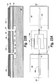
- FIG. 2A is a plan view of a microelectromechanical bulk acoustic resonator containing a resistive heating element, according to an embodiment of the present invention.
- FIG. 2B is a cross-sectional view of the resonator of FIG. 2A , taken along line 2 B- 2 B′.
- FIG. 3A is a plan view of a microelectromechanical bulk acoustic resonator containing a resistive heating element, according to an embodiment of the present invention.
- FIG. 3B is a cross-sectional view of the resonator of FIG. 3A , taken along line 3 B- 3 B′.
- FIGS. 4A-4F are cross-sectional views of intermediate structures that illustrate methods of forming a microelectromechanical bulk acoustic resonator with resistive heating element, according to an embodiment of the invention.
- FIG. 4G is a plan view of the structure of FIG. 4F with the suspended resonator body omitted to highlight a serpentine shape of a resistive heating element, according to an embodiment of the invention.
- FIGS. 5A-5C are cross-sectional views of intermediate structures that illustrate methods of forming a packaged microelectromechanical bulk acoustic resonator with a resistive heating element, according to an embodiment of the invention.
- FIGS. 6A-6B are plan views of microelectromechanical bulk acoustic resonators that utilized patterned electrodes to enhance quality factor, according to embodiments of the present invention.
- FIG. 7A is a plan view of a microelectromechanical bulk acoustic resonator that utilizes materials with positive temperature coefficients of frequency to achieve passive temperature compensation, according to an embodiment of the present invention.
- FIG. 7B is a cross-sectional view of the microelectromechanical bulk acoustic resonator of FIG. 7A , taken along line 7 B- 7 B′.
- FIG. 8A is a plan view of a microelectromechanical bulk acoustic resonator that utilizes materials with positive temperature coefficients of frequency to achieve passive temperature compensation, according to an embodiment of the present invention.
- FIG. 8B is a cross-sectional view of the microelectromechanical bulk acoustic resonator of FIG. 8A , taken along line 8 B- 8 B′.
- FIG. 9A is a plan view of a microelectromechanical bulk acoustic resonator that utilizes materials with positive temperature coefficients of frequency to achieve passive temperature compensation, according to an embodiment of the present invention.
- FIG. 9B is a cross-sectional view of the microelectromechanical bulk acoustic resonator of FIG. 9A , taken along line 9 B- 9 B′.
- FIG. 10A is a plan view of a microelectromechanical bulk acoustic resonator that utilizes materials with positive temperature coefficients of frequency to achieve passive temperature compensation, according to an embodiment of the present invention.
- FIG. 10B is a cross-sectional view of the microelectromechanical bulk acoustic resonator of FIG. 10A , taken along line 10 B- 10 B′.
- FIG. 11A is a plan view of a microelectromechanical bulk acoustic resonator that utilizes materials with positive temperature coefficients of frequency to achieve passive temperature compensation, according to an embodiment of the present invention.
- FIG. 11B is a cross-sectional view of the microelectromechanical bulk acoustic resonator of FIG. 11A , taken along line 11 B- 1 B′.
- FIG. 12A is a plan view of a microelectromechanical bulk acoustic resonator that utilizes materials with positive temperature coefficients of frequency to achieve passive temperature compensation, according to an embodiment of the present invention.
- FIG. 12B is a cross-sectional view of the microelectromechanical bulk acoustic resonator of FIG. 12A , taken along line 12 B- 12 B′.
- FIG. 13A is a plan view of a microelectromechanical bulk acoustic resonator that utilizes materials with positive temperature coefficients of frequency to achieve passive temperature compensation, according to an embodiment of the present invention.
- FIG. 13B is a cross-sectional view of the microelectromechanical bulk acoustic resonator of FIG. 13A , taken along line 13 B- 13 B′.
- FIG. 14A is a plan view of a microelectromechanical bulk acoustic resonator that utilizes materials with positive temperature coefficients of frequency to achieve passive temperature compensation, according to an embodiment of the present invention.
- FIG. 14B is a cross-sectional view of the microelectromechanical bulk acoustic resonator of FIG. 14A , taken along line 14 B- 14 B′.
- FIG. 15A is a plan view of a microelectromechanical bulk acoustic resonator that utilizes materials with positive temperature coefficients of frequency to achieve passive temperature compensation, according to an embodiment of the present invention.
- FIG. 15B is a cross-sectional view of the microelectromechanical bulk acoustic resonator of FIG. 15A , taken along line 15 B- 15 B′.
- FIG. 16A is a plan view of a microelectromechanical bulk acoustic resonator that utilizes materials with positive temperature coefficients of frequency to achieve passive temperature compensation, according to an embodiment of the present invention.
- FIG. 16B is a cross-sectional view of the microelectromechanical bulk acoustic resonator of FIG. 16A , taken along line 16 B- 16 B′.
- FIG. 17A is a plan view of a microelectromechanical bulk acoustic resonator that utilizes materials with positive temperature coefficients of frequency to achieve passive temperature compensation, according to an embodiment of the present invention.
- FIG. 17B is a cross-sectional view of the microelectromechanical bulk acoustic resonator of FIG. 17A , taken along line 17 B- 17 B′.
- FIG. 18A is a plan view of a microelectromechanical bulk acoustic resonator that utilizes materials with positive temperature coefficients of frequency to achieve passive temperature compensation, according to an embodiment of the present invention.
- FIG. 18B is a cross-sectional view of the microelectromechanical bulk acoustic resonator of FIG. 18A , taken along line 18 B- 18 B′.
- FIG. 19A is a plan view of a microelectromechanical bulk acoustic resonator that utilizes materials with positive temperature coefficients of frequency to achieve passive temperature compensation, according to an embodiment of the present invention.
- FIG. 19B is a cross-sectional view of the microelectromechanical bulk acoustic resonator of FIG. 19A , taken along line 19 B- 19 B′.
- FIG. 20A is a plan view of a microelectromechanical bulk acoustic resonator that utilizes materials with positive temperature coefficients of frequency to achieve passive temperature compensation, according to an embodiment of the present invention.
- FIG. 20B is a cross-sectional view of the microelectromechanical bulk acoustic resonator of FIG. 20 , taken along line 20 B- 20 B′.
- FIG. 21A is a plan view of a microelectromechanical bulk acoustic resonator that utilizes materials with positive temperature coefficients of frequency to achieve passive temperature compensation, according to an embodiment of the present invention.
- FIG. 21 is a cross-sectional view of the microelectromechanical bulk acoustic resonator of FIG. 21A , taken along line 21 B- 21 B′.
- FIG. 22A is a plan view of a microelectromechanical bulk acoustic resonator that utilizes materials with positive temperature coefficients of frequency to achieve passive temperature compensation, according to an embodiment of the present invention.
- FIG. 22B is a cross-sectional view of the microelectromechanical bulk acoustic resonator of FIG. 22A , taken along line 22 B- 22 B′.
- FIG. 23A is a plan view of a microelectromechanical bulk acoustic resonator that utilizes materials with positive temperature coefficients of frequency to achieve passive temperature compensation, according to an embodiment of the present invention.
- FIG. 23B is a cross-sectional view of the microelectromechanical bulk acoustic resonator of FIG. 23A , taken along line 23 B- 23 B′.
- first, second, third etc. may be used herein to describe various elements, components, regions, layers and/or sections, these elements, components, regions, layers and/or sections should not be limited by these terms. These terms are only used to distinguish one element, component, region, layer or section from another region, layer or section. Thus, a first element, component, region, layer or section discussed below could be termed a second element, component, region, layer or section without departing from the teachings of the present invention.
- spatially relative terms such as “beneath,” “below,” “lower,” “above,” “upper” and the like, may be used herein for ease of description to describe one element or feature's relationship to another element(s) or feature(s) as illustrated in the figures. It will be understood that the spatially relative terms are intended to encompass different orientations of the device in use or operation in addition to the orientation depicted in the figures. For example, if the device in the figures is turned over, elements described as “below” or “beneath” other elements or features would then be oriented “above” the other elements or features. Thus, the term “below” can encompass both an orientation of above and below. The device may be otherwise oriented (rotated 90 degrees or at other orientations) and the spatially relative descriptors used herein interpreted accordingly.
- Embodiments of the present invention are described herein with reference to cross-section and perspective illustrations that are schematic illustrations of idealized embodiments (and intermediate structures) of the present invention. As such, variations from the shapes of the illustrations as a result, for example, of manufacturing techniques and/or tolerances, are to be expected. Thus, embodiments of the present invention should not be construed as limited to the particular shapes of regions illustrated herein but are to include deviations in shapes that result, for example, from manufacturing. For example, a sharp angle may be somewhat rounded due to manufacturing techniques/tolerances.
- FIGS. 2A-2B illustrate an embodiment of a microelectromechanical resonator formed on a substrate having a recess 103 therein.
- the substrate is illustrated as containing a substrate body 100 (e.g., semiconductor chip) having a resonator body layer 102 thereon, from which a resonator body 102 a (e.g., rectangular monocrystalline silicon body) is patterned and suspended opposite the recess 103 .
- this recess 103 may be defined in a surface of the substrate body 100 in advance of bonding the resonator body layer 102 to the surface.
- This resonator body 102 a may be anchored to the substrate (e.g., surrounding portions of the resonator body layer 102 ) by one or more pairs of tethers (e.g., first and second tethers extending from opposing sides of the resonator body).
- the resonator body layer 102 may also include ledges 102 b that extend over the underlying recess 103 having sidewalls that are recessed relative to sidewalls of the corresponding ledges 102 b.
- the resonator may include a composite stack of the suspended resonator body 102 a , a bottom electrode 104 on the resonator body 102 a , a piezoelectric layer 106 on the bottom electrode 104 and at least a pair of electrodes 108 a , 108 b on the piezoelectric layer 106 .
- the electrodes 108 a , 108 b may include interdigitated fingers as illustrated by FIG. 2A .
- the resonator may further include one or more temperature compensation layers, such as silicon dioxide layers, within the composite stack and one or more perforations (filled or unfilled) within the resonator body 102 a .
- the resonator embodiment of FIGS. 2A-2B further includes a resistive heating element 110 embedded in the ledges 102 b of the resonator body layer 102 .
- This resistive heating element 110 may be formed as a polysilicon or tungsten (W) heating element having a sufficiently low resistance, for example, however, other materials preferably having resistivities in a range from about 10 ⁇ 8 ⁇ m to about 100 ⁇ m.
- Output terminals of a controllable energy source such as a voltage source (V) or a current source (not shown), are applied to a pair of contact pads 110 a , 110 b so that a “frequency tuning” current may be established in the resistive heating element 110 , which is configured to heat the resonator body 102 a by conductive heating of the first and second tethers and further indirectly heat the resonator body 102 a through convective heating of the ambient (e.g., air, nitrogen gas) in the underlying recess 103 .
- the ambient e.g., air, nitrogen gas
- the resistive heating element 110 may be embedded as a square ring-shaped element in a four-sided frame-shaped ledge that overhangs the recess 103 and may thereby surround the resonator body 102 a on at least three sides thereof.
- a resistive heating element may be embodied as first and second resistive heating segments 110 ′ that are at least partially surrounded by a respective one of the first and second thermal isolation trenches 115 , which are illustrated as extending entirely through the corresponding ledges 102 b.
- a substrate 100 e.g., silicon wafer
- a conformal deposition step may be performed to line a bottom and sidewalls of the recess 103 ′ and the upper surface of the substrate 100 within an electrically and thermally insulating oxide or nitride layer 201 (optional).
- a resistive heating material e.g., doped/undoped polysilicon, tungsten (W)
- W tungsten
- the resistive heating element 210 may be patterned as a serpentine-shaped heating element that can convectively heat the resonator body 102 a.
- FIG. 4B illustrates the bonding of the electrically and thermally insulating layer 201 to a resonator body layer 102 .
- This step may be performed by bonding the electrically and thermally insulating layer 201 to a semiconductor-on-insulator (SOI) substrate, which includes a resonator body layer 102 , a sacrificial insulating layer 202 (e.g., oxide layer) and a handling substrate 200 (e.g., silicon wafer).
- SOI semiconductor-on-insulator
- the handling substrate 200 and the sacrificial insulating layer 202 may be removed to expose the resonator body layer 102 using, for example, a sequence of a wafer grinding step and a chemical mechanical polishing (CMP) step to remove the handling substrate 200 and a wet etching step to remove the sacrificial insulating layer 202 without damaging the resonator body layer 102 .
- CMP chemical mechanical polishing
- FIG. 4D illustrates the formation (e.g., deposition and patterning) of a stack of layers on the resonator body layer 102 .
- This stack includes a bottom electrode 104 (e.g., molybdenum (Mo)), a piezoelectric layer 106 (e.g., AlN) on the bottom electrode 104 and at least a pair of electrodes 108 a ′, 108 b ′ on the piezoelectric layer 106 .
- a bottom electrode 104 e.g., molybdenum (Mo)
- a piezoelectric layer 106 e.g., AlN
- first and second electrical interconnects 212 a , 212 b illustrates the formation of first and second electrical interconnects 212 a , 212 b on underlying portions of the resistive heating element 210 (e.g., on opposing ends of a serpentine-shaped heating element) and the formation of contact pads 214 a , 214 b on the electrical interconnects 212 a , 212 b .
- the formation of the first and second electrical interconnects 212 a , 212 b may be preceded by the formation of openings/vias in the resonator body layer 102 , which are then filled with the material of the electrical interconnects 212 a , 212 b .
- the electrical interconnects 212 a , 212 b may be formed of a material having a higher electrical conductivity relative to the material of the resistive heating element 210 .
- the electrical interconnects 212 a , 212 b are preferably formed using materials that require relatively low temperature processing (e.g., back-end processing), which will not damage the previously formed materials of the resonator.
- deep trenches are etched through the resonator body layer 102 to: (i) define a suspended resonator body 102 a , which is anchored opposite the recess 103 ′ by at least a pair of tethers to surrounding portions of the resonator body layer 102 ; and (ii) define thermal and electrical isolation trenches 115 , which substantially surround corresponding electrical interconnects 212 a , 212 b .
- the passing of a current through the resistive heating element 210 causes convective heating of the ambient (e.g., air, nitrogen gas) in the recess 103 ′ during resonant operation of the resonator.
- This current may be controlled to thereby adjust a temperature of the resonator and its resonant frequency.
- methods of forming a packaged microelectromechanical bulk acoustic resonator may include forming a recess in a surface of a capping substrate 300 (e.g., silicon substrate) and then lining the recess and the surface of the capping substrate with an electrically and thermally insulating layer 201 , as illustrated by FIG. 5A . Thereafter, a resistive heating element 210 (e.g., a serpentine-shaped element) may be formed on the insulating layer 201 within the recess.
- a bonding material may also be deposited onto the insulating layer 201 and then patterned to define a bonding pattern 250 (e.g., ring-shaped bonding pattern).
- a substrate 100 containing a resonator body layer 102 associated with a suspended microelectromechanical resonator may be bonded to the bonding pattern 250 to thereby define a sealed cavity 125 (e.g., a hermetically sealed cavity), which shares an ambient with the recess 103 .
- a selective etching step may be performed to define contact openings/vias in the capping substrate 300 , which expose respective portions of the resistive heating element 210 .
- First and second electrical interconnects 212 a ′, 212 b ′ may then be formed in the contact openings, as illustrated, and then contact pads 214 a ′, 214 b ′ may be formed on the interconnects 212 a ′, 212 b ′.
- the passing of a externally controlled current through the resistive heating element 210 causes convective heating of the ambient (e.g., air, nitrogen gas) in the sealed cavity 125 during resonant operation of the resonator.
- the ambient e.g., air, nitrogen gas
- FIGS. 6A-6B are plan views of microelectromechanical bulk acoustic resonators that utilize uniquely shaped electrodes to enhance quality factor, according to embodiments of the present invention.
- FIGS. 6A-6B illustrate resonators having electrodes ( 118 a , 118 b ) and ( 118 a ′, 118 b ′) thereon, which are patterned to achieve an optimized or nearly optimized balance between high resonator quality (Q) resulting from relatively small surface/interface loss (achieved by small electrode area on the resonator surface) and low motional impedance (e.g., low insertion loss) resulting from higher piezoelectric coupling (achieved by sufficiently large electrode area on the resonator surface).
- Q resonator quality
- FIG. 6A illustrates a resonator including a resonator body 102 a anchored to a surrounding substrate 102 by a pair of tethers and a pair of facing C-shaped input and output electrodes 118 a and 118 b that extend adjacent outer edges of the resonator body 102 a when viewed from a top down perspective.
- FIG. 6B illustrates a resonator including a resonator body 102 a anchored to a surrounding substrate 102 by a pair of tethers and a pair input and output electrodes 118 a ′ and 118 b ′.
- the input electrode 118 a ′ may be rectangular shaped electrode located at a center of the resonator body 102 a and the output electrode 118 b ′ may be a four-sided frame-shaped electrode that extends adjacent outer edges of the resonator body 102 a and substantially surrounds the input electrode 118 a′
- FIGS. 7A-7B a microelectromechanical bulk acoustic resonator will be described that utilizes additional materials with positive temperature coefficients of frequency to achieve passive temperature compensation.
- FIGS. 7A-7B illustrate a resonator containing a composite stack of a resonator body 102 a (e.g., silicon body), a bottom electrode 104 (e.g., Mo electrode) on the resonator body 102 a , a piezoelectric layer 106 (e.g., AlN layer) on the bottom electrode 104 and a pair of top electrodes 108 a , 108 b on the piezoelectric layer 106 , which contain interdigitated fingers that partially cover a surface of the piezoelectric layer 106 .
- a resonator body 102 a e.g., silicon body
- a bottom electrode 104 e.g., Mo electrode
- a piezoelectric layer 106 e.g., AlN layer
- first and second electrically insulating layers 140 a , 142 a e.g., silicon dioxide layers
- TCFs positive temperature coefficients of frequency
- These layers 140 a , 142 a can be provided to achieve passive temperature compensation while simultaneously balancing mechanical stresses on the resonator body 102 a and also preventing the layers 140 a , 142 a from becoming the dominant resonating layers by virtue of the relatively high acoustic loss characteristics of the layers 140 a , 142 a .
- the resonator may be anchored to a surrounding substrate using a single pair of tethers 50 .
- This substrate is illustrated as including a substrate body 100 having a first electrically insulating layer 140 thereon, a resonator body layer 102 on the insulating layer 140 and a second electrically insulating layer 142 on the resonator body layer 102 .
- the total thicknesses of the first and second electrically insulating layers 140 a , 142 a may be chosen based on the following analytical expression applicable to a four material composite structure (e.g., SiO 2 , Mo, AlN, Si), where ppm n represents material n's temperature coefficient of elasticity (TCE), t n represents material n's thickness and E n represents material n's Young's modulus:
- ppm ( ppm 1 + 1 ) 2 ⁇ E 1 ⁇ t 1 + ( ppm 2 + 1 ) 2 ⁇ E 2 ⁇ t 2 + ( ppm 3 + 1 ) 2 ⁇ E 3 ⁇ t 3 + ( ppm 4 + 1 ) 2 ⁇ E 4 ⁇ t 4 E 1 ⁇ t 1 + E 2 ⁇ t 2 + E 3 ⁇ t 3 + E 4 ⁇ t 4 - 1
- FIGS. 8A-8B illustrate a microelectromechanical bulk acoustic resonator that is similar to the resonator of FIGS. 7A-7B , but includes longer interdigitated electrodes and an asymmetric arrangement of two tethers 50 that support the first electrode 108 a at two nodal lines and one tether 50 that supports the second electrode 108 b at a central nodal line.
- FIGS. 9A-9B illustrate a microelectromechanical bulk acoustic resonator that is similar to the resonator of FIGS.
- FIGS. 10A-10B illustrate a microelectromechanical bulk acoustic resonator that is similar to the resonator of FIGS. 9A-9B , but includes a different asymmetric arrangement of two tethers 50 that support the second electrode 108 b at two nodal lines and two tethers 50 that support the first electrode 108 a at two different nodal lines.
- FIGS. 11A-11B illustrate a microelectromechanical bulk acoustic resonator that is similar to the resonator of FIGS. 10A-10B , but includes a different symmetrical arrangement of two tethers 50 that support the second electrode 108 b at two nodal lines and two tethers 50 that support the first electrode 108 a at the same two nodal lines.
- FIGS. 12A-12B illustrate a microelectromechanical bulk acoustic resonator that is similar to the resonator of FIGS.
- FIGS. 13A-13B illustrate a microelectromechanical bulk acoustic resonator that is similar to the resonator of FIGS. 12A-12B , but includes a different asymmetrical arrangement of three tethers 50 that support the second electrode 108 b at three nodal lines and two tethers 50 that support the first electrode 108 a at two nodal lines, which overlap with two of three nodal lines.
- FIGS. 14A-14B illustrate a microelectromechanical bulk acoustic resonator that is similar to the resonator of FIGS. 13A-13B , but includes a different asymmetrical arrangement of three tethers 50 that support the second electrode 108 b at three nodal lines (including the center nodal line) and three tethers 50 that support the first electrode 108 a at three nodal lines (including the center nodal line).
- FIGS. 15A-15B illustrate a microelectromechanical bulk acoustic resonator that is similar to the resonator of FIGS.
- FIGS. 16A-16B illustrate a microelectromechanical bulk acoustic resonator that is similar to the resonator of FIGS. 12A-12B , but includes a different asymmetrical arrangement of three tethers 50 that support the second electrode 108 b at three nodal lines (including the center nodal line) and four tethers 50 on the other side that support the first electrode 108 a at two nodal lines.
- FIGS. 17A-17B illustrate a microelectromechanical bulk acoustic resonator that is similar to the resonator of FIGS.
- 16A-16B but includes a different asymmetrical arrangement of three tethers 50 that support the second electrode 108 b at three nodal lines (including the center nodal line) and four tethers 50 on the other side that support the first electrode 108 a at two nodal lines that overlap with two of the three nodal lines associated with the second electrode 108 b.
- FIGS. 18A-18B illustrate a microelectromechanical bulk acoustic resonator that includes a symmetric arrangement of four tethers on both sides of the resonator body 102 a , but where the second electrode 108 b is supported at four nodal lines (not including the center nodal line) and the first electrode 108 a is supported at two nodal lines (not including the center nodal line).
- FIGS. 18A-18B illustrate a microelectromechanical bulk acoustic resonator that includes a symmetric arrangement of four tethers on both sides of the resonator body 102 a , but where the second electrode 108 b is supported at four nodal lines (not including the center nodal line) and the first electrode 108 a is supported at two nodal lines (not including the center nodal line).
- FIGS. 18A-18B illustrate a microelectromechanical bulk acoustic resonator that includes a symmetric arrangement of
- FIGS. 20A-20B illustrate a microelectromechanical bulk acoustic resonator that includes an asymmetric arrangement of five tethers that support second electrode 108 b at five nodal lines (including the center nodal line) and four tethers on the other side that support the first electrode 108 a at two nodal lines (not including the center nodal line).
- FIGS. 20A-20B illustrate a microelectromechanical bulk acoustic resonator that includes a symmetric arrangement of five tethers that support second electrode 108 b at five nodal lines (including the center nodal line) and five tethers that support the first electrode 108 a at three nodal lines (including the center nodal line).
- FIGS. 21A-21B illustrate a microelectromechanical bulk acoustic resonator that includes reduced area electrodes with interdigitated fingers (long and short) that are patterned to achieve an optimized or nearly optimized balance between high resonator quality (Q) resulting from relatively small surface/interface loss (achieved by small electrode area on the resonator surface) and low motional impedance (e.g., low insertion loss) resulting from higher piezoelectric coupling (achieved by sufficiently large electrode area on the resonator surface).
- Q resonator quality
- FIGS. 22A-22B illustrate a microelectromechanical bulk acoustic resonator that includes reduced area electrodes with partially overlapping interdigitated fingers having the same length, which are patterned to achieve an optimized or nearly optimized balance between high resonator quality (Q) resulting from relatively small surface/interface loss (achieved by small electrode area on the resonator surface) and low motional impedance (e.g., low insertion loss) resulting from higher piezoelectric coupling (achieved by sufficiently large electrode area on the resonator surface).
- Q resonator quality
- 23A-23B illustrate a microelectromechanical bulk acoustic resonator that includes reduced area electrodes with fully overlapping interdigitated fingers having the same length, which are patterned to achieve an optimized or nearly optimized balance between high resonator quality (Q) resulting from relatively small surface/interface loss (achieved by small electrode area on the resonator surface) and low motional impedance (e.g., low insertion loss) resulting from higher piezoelectric coupling (achieved by sufficiently large electrode area on the resonator surface).
- Q resonator quality
Landscapes
- Engineering & Computer Science (AREA)
- Manufacturing & Machinery (AREA)
- Physics & Mathematics (AREA)
- Acoustics & Sound (AREA)
- Piezo-Electric Or Mechanical Vibrators, Or Delay Or Filter Circuits (AREA)
- Micromachines (AREA)
Abstract
Description
Claims (8)
Priority Applications (2)
| Application Number | Priority Date | Filing Date | Title |
|---|---|---|---|
| US13/250,560 US8610336B1 (en) | 2011-09-30 | 2011-09-30 | Microelectromechanical resonators having resistive heating elements therein configured to provide frequency tuning through convective heating of resonator bodies |
| US13/407,484 US8638178B1 (en) | 2011-09-30 | 2012-02-28 | Methods of testing packaged thin-film piezoelectric-on-semiconductor microelectromechanical resonators having hermetic seals |
Applications Claiming Priority (1)
| Application Number | Priority Date | Filing Date | Title |
|---|---|---|---|
| US13/250,560 US8610336B1 (en) | 2011-09-30 | 2011-09-30 | Microelectromechanical resonators having resistive heating elements therein configured to provide frequency tuning through convective heating of resonator bodies |
Related Child Applications (1)
| Application Number | Title | Priority Date | Filing Date |
|---|---|---|---|
| US13/407,484 Continuation-In-Part US8638178B1 (en) | 2011-09-30 | 2012-02-28 | Methods of testing packaged thin-film piezoelectric-on-semiconductor microelectromechanical resonators having hermetic seals |
Publications (1)
| Publication Number | Publication Date |
|---|---|
| US8610336B1 true US8610336B1 (en) | 2013-12-17 |
Family
ID=49725744
Family Applications (1)
| Application Number | Title | Priority Date | Filing Date |
|---|---|---|---|
| US13/250,560 Expired - Fee Related US8610336B1 (en) | 2011-09-30 | 2011-09-30 | Microelectromechanical resonators having resistive heating elements therein configured to provide frequency tuning through convective heating of resonator bodies |
Country Status (1)
| Country | Link |
|---|---|
| US (1) | US8610336B1 (en) |
Cited By (6)
| Publication number | Priority date | Publication date | Assignee | Title |
|---|---|---|---|---|
| US20120181900A1 (en) * | 2011-01-13 | 2012-07-19 | Delaware Capital Formation, Inc. | Sensors for measuring at least one of pressure and temperature, sensor arrays and related methods |
| US20130342263A1 (en) * | 2012-06-26 | 2013-12-26 | Thorsten Meyer | Heater for semiconductor device |
| US9167351B1 (en) * | 2011-06-15 | 2015-10-20 | Hrl Laboratories, Llc | Heated quartz crystal resonator with strain isolation and method of fabricating same |
| US20170275158A1 (en) * | 2016-03-23 | 2017-09-28 | Invensense, Inc. | Integration of ain ultrasonic transducer on a cmos substrate using fusion bonding process |
| US20180044173A1 (en) * | 2016-08-15 | 2018-02-15 | Y-Sensors Ltd. | Temperature stabilized mems device |
| US20220081281A1 (en) * | 2019-02-12 | 2022-03-17 | Robert Bosch Gmbh | Micromechanical sensor device and corresponding manufacturing method |
Citations (51)
| Publication number | Priority date | Publication date | Assignee | Title |
|---|---|---|---|---|
| US5160901A (en) | 1990-09-13 | 1992-11-03 | Frequency Electronics, Inc. | Multimode crystal oscillator |
| US5229735A (en) | 1992-03-30 | 1993-07-20 | Macrovision Corporation | Wide frequency deviation voltage controlled crystal oscillator having plural parallel crystals |
| US5640133A (en) | 1995-06-23 | 1997-06-17 | Cornell Research Foundation, Inc. | Capacitance based tunable micromechanical resonators |
| US6049256A (en) * | 1998-09-10 | 2000-04-11 | Cts Corporation | Low profile ovenized oscillator packing having a high thermal conductivity substrate |
| EP1217735A1 (en) | 2000-12-21 | 2002-06-26 | Eta SA Fabriques d'Ebauches | Time base comprising an integrated micromechanical tuning fork resonator |
| US20020096967A1 (en) | 2000-02-18 | 2002-07-25 | Qing Ma | Micro-electromechanical structure resonator, method of making, and method of using |
| US6557419B1 (en) | 1996-12-31 | 2003-05-06 | Honeywell International Inc. | Zero TCF thin film resonator |
| US6604266B1 (en) | 1997-06-24 | 2003-08-12 | Tdk Corporation | Manufacturing method for a piezoelectric component |
| US6630871B2 (en) | 2001-09-28 | 2003-10-07 | Intel Corporation | Center-mass-reduced microbridge structures for ultra-high frequency MEM resonator |
| US6657363B1 (en) | 1998-05-08 | 2003-12-02 | Infineon Technologies Ag | Thin film piezoelectric resonator |
| US6731180B1 (en) * | 2000-10-20 | 2004-05-04 | Deleware Capital Formation Inc. | Evacuated hybrid ovenized oscillator |
| US6734762B2 (en) * | 2001-04-09 | 2004-05-11 | Motorola, Inc. | MEMS resonators and method for manufacturing MEMS resonators |
| US6739190B2 (en) | 2000-08-24 | 2004-05-25 | The Regents Of The University Of Michigan | Micromechanical resonator device |
| US6870444B1 (en) | 2003-08-28 | 2005-03-22 | Motorola, Inc. | Electromechanical resonator and method of operating same |
| US20050146248A1 (en) | 2003-11-20 | 2005-07-07 | Moler Jeffery B. | Integral thermal compensation for an electro-mechanical actuator |
| US20050242904A1 (en) | 2004-04-28 | 2005-11-03 | Markus Lutz | Method for adjusting the frequency of a MEMS resonator |
| US20060125576A1 (en) | 2004-10-18 | 2006-06-15 | Ho Gavin K | Highly tunable low-impedance capacitive micromechanical resonators, oscillators, and processes relating thereto |
| US7071793B2 (en) | 2003-04-16 | 2006-07-04 | Robert Bosch Gmbh | Temperature compensation for silicon MEMS resonator |
| US20060196273A1 (en) | 2004-12-12 | 2006-09-07 | Burns David W | Optically coupled resonator |
| US20060225504A1 (en) | 2005-01-29 | 2006-10-12 | Farrokh Ayazi | Resonating star gyroscope and fabrication methods |
| US7176770B2 (en) | 2004-08-24 | 2007-02-13 | Georgia Tech Research Corp. | Capacitive vertical silicon bulk acoustic resonator |
| US20070069612A1 (en) | 2005-08-30 | 2007-03-29 | Epson Toyocom Corporation | Piezoelectric resonator and adjustment method |
| US7199504B2 (en) | 2000-11-29 | 2007-04-03 | Tdk Corporation | Film bulk acoustic resonator filter |
| US7215061B2 (en) | 2003-12-04 | 2007-05-08 | Seiko Epson Corporation | Micromechanical electrostatic resonator |
| WO2007072409A2 (en) | 2005-12-23 | 2007-06-28 | Nxp B.V. | A mems resonator, a method of manufacturing thereof, and a mems oscillator |
| US20070220971A1 (en) | 2006-03-27 | 2007-09-27 | Georgia Tech Research Corporation | Capacitive bulk acoustic wave disk gyroscopes |
| US7280007B2 (en) | 2004-11-15 | 2007-10-09 | Avago Technologies General Ip (Singapore) Pte. Ltd. | Thin film bulk acoustic resonator with a mass loaded perimeter |
| US20070277620A1 (en) | 2006-06-02 | 2007-12-06 | Renata Melamud | Composite mechanical transducers and approaches therefor |
| US7312674B2 (en) | 2002-08-06 | 2007-12-25 | The Charles Stark Draper Laboratory, Inc. | Resonator system with a plurality of individual mechanically coupled resonators and method of making same |
| US20080143217A1 (en) | 2006-12-13 | 2008-06-19 | Gavin Kar-Fai Ho | Process compensated micromechanical resonators |
| US20080186109A1 (en) | 2006-12-13 | 2008-08-07 | Gavin Kar-Fai Ho | Low frequency process-variation-insensitive termperature-stable micromechanical resonators |
| US7446620B2 (en) | 2006-06-14 | 2008-11-04 | Sitime Corporation | Microelectromechanical oscillator having temperature measurement system, and method of operating same |
| US7489063B2 (en) | 2006-07-31 | 2009-02-10 | Hitachi Media Electronics Co., Ltd. | Thin film piezoelectric bulk acoustic wave resonator and radio frequency filter using the same |
| US7514852B2 (en) * | 2005-06-24 | 2009-04-07 | Nihon Dempa Kogyo Co., Ltd. | Piezooscillator |
| US20090153267A1 (en) | 2007-12-18 | 2009-06-18 | Markus Lutz | MEMS resonator structure and method |
| US20090160581A1 (en) | 2007-12-21 | 2009-06-25 | Paul Merritt Hagelin | Temperature Stable MEMS Resonator |
| US7608980B2 (en) | 2006-09-05 | 2009-10-27 | Canon Kabushiki Kaisha | Vibration control apparatus and method |
| US7616077B1 (en) | 2007-03-22 | 2009-11-10 | Sandia Corporation | Microelectromechanical resonator and method for fabrication |
| US7639104B1 (en) | 2007-03-09 | 2009-12-29 | Silicon Clocks, Inc. | Method for temperature compensation in MEMS resonators with isolated regions of distinct material |
| US7639105B2 (en) * | 2007-01-19 | 2009-12-29 | Georgia Tech Research Corporation | Lithographically-defined multi-standard multi-frequency high-Q tunable micromechanical resonators |
| EP2144369A1 (en) | 2008-07-11 | 2010-01-13 | St Microelectronics S.A. | Bulk acoustic wave resonator |
| US20100032789A1 (en) | 2008-08-07 | 2010-02-11 | Infineon Technologies Ag | Passive temperature compensation of silicon mems devices |
| US7675389B2 (en) | 2005-06-29 | 2010-03-09 | Panasonic Corporation | Piezoelectric resonator, piezoelectric filter, and duplexer and communication device using the same |
| US20100060384A1 (en) | 2008-09-09 | 2010-03-11 | Fujitsu Limited | Filter, duplexer and communication apparatus |
| US20100194241A1 (en) | 2009-01-30 | 2010-08-05 | Integrated Device Technology, Inc. | Thin-film bulk acoustic resonators having perforated bodies that provide reduced susceptibility to process-induced lateral dimension variations |
| US20100225405A1 (en) * | 2009-03-09 | 2010-09-09 | Eta Sa Manufacture Horlogere Suisse | Oscillator device comprising a thermally-controlled piezoelectric resonator |
| US20100319185A1 (en) | 2009-06-19 | 2010-12-23 | Farrokh Ayazi | Methods of Forming Micromechanical Resonators Having High Density Trench Arrays Therein that Provide Passive Temperature Compensation |
| US7888843B2 (en) | 2008-09-10 | 2011-02-15 | Georgia Tech Research Corporation | Thin-film piezoelectric-on-insulator resonators having perforated resonator bodies therein |
| US20110175492A1 (en) * | 2010-01-21 | 2011-07-21 | Imec | Temperature Compensation Device and Method for MEMS Resonator |
| US7990025B1 (en) * | 2004-09-01 | 2011-08-02 | Pablo Ferreiro | Silicon package with embedded oscillator |
| US8106724B1 (en) * | 2009-07-23 | 2012-01-31 | Integrated Device Technologies, Inc. | Thin-film bulk acoustic resonators having perforated resonator body supports that enhance quality factor |
-
2011
- 2011-09-30 US US13/250,560 patent/US8610336B1/en not_active Expired - Fee Related
Patent Citations (54)
| Publication number | Priority date | Publication date | Assignee | Title |
|---|---|---|---|---|
| US5160901A (en) | 1990-09-13 | 1992-11-03 | Frequency Electronics, Inc. | Multimode crystal oscillator |
| US5229735A (en) | 1992-03-30 | 1993-07-20 | Macrovision Corporation | Wide frequency deviation voltage controlled crystal oscillator having plural parallel crystals |
| US5640133A (en) | 1995-06-23 | 1997-06-17 | Cornell Research Foundation, Inc. | Capacitance based tunable micromechanical resonators |
| US6557419B1 (en) | 1996-12-31 | 2003-05-06 | Honeywell International Inc. | Zero TCF thin film resonator |
| US6604266B1 (en) | 1997-06-24 | 2003-08-12 | Tdk Corporation | Manufacturing method for a piezoelectric component |
| US6657363B1 (en) | 1998-05-08 | 2003-12-02 | Infineon Technologies Ag | Thin film piezoelectric resonator |
| US6049256A (en) * | 1998-09-10 | 2000-04-11 | Cts Corporation | Low profile ovenized oscillator packing having a high thermal conductivity substrate |
| US20020096967A1 (en) | 2000-02-18 | 2002-07-25 | Qing Ma | Micro-electromechanical structure resonator, method of making, and method of using |
| US6739190B2 (en) | 2000-08-24 | 2004-05-25 | The Regents Of The University Of Michigan | Micromechanical resonator device |
| US6731180B1 (en) * | 2000-10-20 | 2004-05-04 | Deleware Capital Formation Inc. | Evacuated hybrid ovenized oscillator |
| US7199504B2 (en) | 2000-11-29 | 2007-04-03 | Tdk Corporation | Film bulk acoustic resonator filter |
| EP1217735A1 (en) | 2000-12-21 | 2002-06-26 | Eta SA Fabriques d'Ebauches | Time base comprising an integrated micromechanical tuning fork resonator |
| US6734762B2 (en) * | 2001-04-09 | 2004-05-11 | Motorola, Inc. | MEMS resonators and method for manufacturing MEMS resonators |
| US6630871B2 (en) | 2001-09-28 | 2003-10-07 | Intel Corporation | Center-mass-reduced microbridge structures for ultra-high frequency MEM resonator |
| US7312674B2 (en) | 2002-08-06 | 2007-12-25 | The Charles Stark Draper Laboratory, Inc. | Resonator system with a plurality of individual mechanically coupled resonators and method of making same |
| US20070188269A1 (en) | 2003-04-16 | 2007-08-16 | Markus Lutz | Temperature compensation for silicon MEMS resonator |
| US7071793B2 (en) | 2003-04-16 | 2006-07-04 | Robert Bosch Gmbh | Temperature compensation for silicon MEMS resonator |
| US7202761B2 (en) | 2003-04-16 | 2007-04-10 | Robert Bosch Gmbh | Temperature compensation for silicon MEMS resonator |
| US6870444B1 (en) | 2003-08-28 | 2005-03-22 | Motorola, Inc. | Electromechanical resonator and method of operating same |
| US20050146248A1 (en) | 2003-11-20 | 2005-07-07 | Moler Jeffery B. | Integral thermal compensation for an electro-mechanical actuator |
| US7215061B2 (en) | 2003-12-04 | 2007-05-08 | Seiko Epson Corporation | Micromechanical electrostatic resonator |
| US20050242904A1 (en) | 2004-04-28 | 2005-11-03 | Markus Lutz | Method for adjusting the frequency of a MEMS resonator |
| US7176770B2 (en) | 2004-08-24 | 2007-02-13 | Georgia Tech Research Corp. | Capacitive vertical silicon bulk acoustic resonator |
| US7990025B1 (en) * | 2004-09-01 | 2011-08-02 | Pablo Ferreiro | Silicon package with embedded oscillator |
| US20060125576A1 (en) | 2004-10-18 | 2006-06-15 | Ho Gavin K | Highly tunable low-impedance capacitive micromechanical resonators, oscillators, and processes relating thereto |
| US7280007B2 (en) | 2004-11-15 | 2007-10-09 | Avago Technologies General Ip (Singapore) Pte. Ltd. | Thin film bulk acoustic resonator with a mass loaded perimeter |
| US20060196273A1 (en) | 2004-12-12 | 2006-09-07 | Burns David W | Optically coupled resonator |
| US20060225504A1 (en) | 2005-01-29 | 2006-10-12 | Farrokh Ayazi | Resonating star gyroscope and fabrication methods |
| US7514852B2 (en) * | 2005-06-24 | 2009-04-07 | Nihon Dempa Kogyo Co., Ltd. | Piezooscillator |
| US7675389B2 (en) | 2005-06-29 | 2010-03-09 | Panasonic Corporation | Piezoelectric resonator, piezoelectric filter, and duplexer and communication device using the same |
| US20070069612A1 (en) | 2005-08-30 | 2007-03-29 | Epson Toyocom Corporation | Piezoelectric resonator and adjustment method |
| WO2007072409A2 (en) | 2005-12-23 | 2007-06-28 | Nxp B.V. | A mems resonator, a method of manufacturing thereof, and a mems oscillator |
| US20070220971A1 (en) | 2006-03-27 | 2007-09-27 | Georgia Tech Research Corporation | Capacitive bulk acoustic wave disk gyroscopes |
| US20070277620A1 (en) | 2006-06-02 | 2007-12-06 | Renata Melamud | Composite mechanical transducers and approaches therefor |
| US7446620B2 (en) | 2006-06-14 | 2008-11-04 | Sitime Corporation | Microelectromechanical oscillator having temperature measurement system, and method of operating same |
| US7489063B2 (en) | 2006-07-31 | 2009-02-10 | Hitachi Media Electronics Co., Ltd. | Thin film piezoelectric bulk acoustic wave resonator and radio frequency filter using the same |
| US7608980B2 (en) | 2006-09-05 | 2009-10-27 | Canon Kabushiki Kaisha | Vibration control apparatus and method |
| US20080143217A1 (en) | 2006-12-13 | 2008-06-19 | Gavin Kar-Fai Ho | Process compensated micromechanical resonators |
| US20080186109A1 (en) | 2006-12-13 | 2008-08-07 | Gavin Kar-Fai Ho | Low frequency process-variation-insensitive termperature-stable micromechanical resonators |
| US7639105B2 (en) * | 2007-01-19 | 2009-12-29 | Georgia Tech Research Corporation | Lithographically-defined multi-standard multi-frequency high-Q tunable micromechanical resonators |
| US7639104B1 (en) | 2007-03-09 | 2009-12-29 | Silicon Clocks, Inc. | Method for temperature compensation in MEMS resonators with isolated regions of distinct material |
| US7616077B1 (en) | 2007-03-22 | 2009-11-10 | Sandia Corporation | Microelectromechanical resonator and method for fabrication |
| US20090153267A1 (en) | 2007-12-18 | 2009-06-18 | Markus Lutz | MEMS resonator structure and method |
| US20090160581A1 (en) | 2007-12-21 | 2009-06-25 | Paul Merritt Hagelin | Temperature Stable MEMS Resonator |
| EP2144369A1 (en) | 2008-07-11 | 2010-01-13 | St Microelectronics S.A. | Bulk acoustic wave resonator |
| US20100032789A1 (en) | 2008-08-07 | 2010-02-11 | Infineon Technologies Ag | Passive temperature compensation of silicon mems devices |
| US20100060384A1 (en) | 2008-09-09 | 2010-03-11 | Fujitsu Limited | Filter, duplexer and communication apparatus |
| US7888843B2 (en) | 2008-09-10 | 2011-02-15 | Georgia Tech Research Corporation | Thin-film piezoelectric-on-insulator resonators having perforated resonator bodies therein |
| US20100194241A1 (en) | 2009-01-30 | 2010-08-05 | Integrated Device Technology, Inc. | Thin-film bulk acoustic resonators having perforated bodies that provide reduced susceptibility to process-induced lateral dimension variations |
| US7939990B2 (en) | 2009-01-30 | 2011-05-10 | Integrated Device Technology, Inc. | Thin-film bulk acoustic resonators having perforated bodies that provide reduced susceptibility to process-induced lateral dimension variations |
| US20100225405A1 (en) * | 2009-03-09 | 2010-09-09 | Eta Sa Manufacture Horlogere Suisse | Oscillator device comprising a thermally-controlled piezoelectric resonator |
| US20100319185A1 (en) | 2009-06-19 | 2010-12-23 | Farrokh Ayazi | Methods of Forming Micromechanical Resonators Having High Density Trench Arrays Therein that Provide Passive Temperature Compensation |
| US8106724B1 (en) * | 2009-07-23 | 2012-01-31 | Integrated Device Technologies, Inc. | Thin-film bulk acoustic resonators having perforated resonator body supports that enhance quality factor |
| US20110175492A1 (en) * | 2010-01-21 | 2011-07-21 | Imec | Temperature Compensation Device and Method for MEMS Resonator |
Non-Patent Citations (28)
| Title |
|---|
| "Film Bulk Acoustic-Wave Resonator (FBAR)," Admitted Prior Art, http://mems.usc.edu/fbar.htm, Printed from the Internet Oct. 14, 2008, 3 pages. |
| "Finite element method," Admitted Prior Art, http://en.wikipedia.org/wiki/ Finite-element-method, Printed from the Internet Nov. 3, 2011, 13 pages. |
| Abdolvand et al., "A Low Voltage Temperature-Stable Micromechanical Piezoelectric Oscillator," Digest of the 14th International Conference on Solid State Sensors, Actuators and Microsystems (Transducers '07), Lyon, France, Jun. 2007, pp, 53-56. |
| Abdolvand et al., "A Temperature-Compensated ZnO-on-Diamond Resonant Mass Sensor," Proc. 5th IEEE Conference on Sensors, 2006, pp. 1297-1300. |
| Abdolvand et al., "Single-Resonator Dual-Frequency Thin-Film Piezoelectric-on-Substrate Oscillator", IEEE International Electron Devices Meeting, 2007, pp. 419-422. |
| Baborowski et al., "Piezoelectrically Activated Silicon Resonators", IEEE Frequency Control Symposium, 2007 Joint with the 21st European Frequency and Time Forum, May 1, 2007, pp. 1210-1213, XP031138158, section I. |
| Casinovi et al., "Analytical Modeling and Numerical Simulation of Capacitive Silicon Bulk Acoustic Resonators," IEEE International Conference on Micro Electro Mechanical Systems, Jan. 2009, pp. 935-938. |
| Dubois, Marc-Alexandre., "Thin film bulk acoustic wave resonators: a technology overview," MEMSWAVE 03, Toulouse, France, Jul. 2-4, 2003. |
| Ho et al., "High Order Composite Bulk Acoustic Resonators," Proc. 20th IEEE International Conference on Micro Electro Mechanical Systems (MEMS '07), Kobe, Japan, Jan. 2007, pp. 791-794. |
| Ho et al., "Temperature Compensated IBAR Reference Oscillators," Proc. 19th IEEE International Conference on Micro Electro Mechanical System,(MEMS '06), Istanbul, Turkey, Jan. 2006, pp. 910-913. |
| Invitation to Pay Additional Fees and, Where Applicable, Protest Fee, PCT/US2010/022510, Jun. 4, 2010. |
| Jaakkola et al., "Piezoelectrically transduced Single-Crystal-Silicon Plate Resonators," VTT Technical Research Centre of Finland, Finland. |
| Kim et al., "Micromechanical Resonant Displacement Gain Stages," IEEE, 2009, pp. 19-22. |
| Kim et al., "Temperature Dependence of Quality Factor in MEMS Resonators," Journal of Microelectromechanical Systems, vol. 17, No. 3, Jun. 2008, pp. 755-766. |
| Lin et al., "Series-Resonant VHF Micromechanical Resonator Reference Oscillators," IEEE Journal of Solid-State Circuits, vol. 39, No. 12, Dec. 2004, pp. 2477-2491. |
| Luoto et al., "MEMS on cavity-SOI wafers," Solid State Electronics 51:328-332 (2007). |
| Nam et al., "Piezoelectric Properties of Aluminum Nitride for Thin Film Bulk Acoustic Wave Resonator," J. Korean Physical Society, 47:S309-S312 (2005). |
| Notification of Transmittal of the International Search Report and the Written Opinion of the International Searching Authority , or the Declaration, International Search Report, Written Opinion of the International Searching Authority, PCT/US2010/037429, Date of Mailing: Sep. 6, 2010, 28 pages. |
| Notification of Transmittal of the International Search Report and the Written Opinion of the International Searching Authority, or the Declaration, Written Opinion of the International Searching Authority, International Application No, PCT/US2010/022510, date of mailing Aug. 25, 2010, 19 pages. |
| Notification of Transmittal of the International Search Report and the Written Opinion of the International Searching Authority, or the Declaration; International Search Report; Written Opinion of the International Searching Authority, PCT Application No. PCT/US2008/010844, Jun. 24, 2009. |
| Pourkamali et al., "Low-impedance VHF and UHF Capacitive Silicon Bulk Acoustic Wave Resonators-Part I: Concept and Fabrication," IEEE Transaction on Electron Devices, vol. 54, No. 8, Aug. 2007, pp. 2017-2023. |
| Samarao et al. (2010) "Intrinsic Temperature Compensation of Highly Resistive High-Q Silicon Microresonators Via Charge Carrier Depletion", Frequency Control Symposium (FCS), 2010 IEEE International, Jun. 1-4, 2010, Newport Beach, California, pp. 334-339. |
| Samarao et al. (2010) "Passive TCF Compensation in High Q Silicon Micromechanical Resonators", IEEE International Conference on Micro Electro Mechanical Systems, Jan. 2010, pp. 116-119. |
| Schodowski, "Resonator Self-Temperature-Sensing Using A Dual-Harmonic-Mode Crystal Oscillator," Proc. of the 43rd Annual Symposium on Frequency Control, Jun. 1989, pp. 2-7. |
| Schoen et al., "Temperature Compensation in Silicon-Based Micro-Electromechanical Resonators", IEEE Conference on Micro Electromechanical Systems 2009, Jan. 25, 2009, pp. 884-887, XP031444436, figures 1-3. |
| Sundaresan et al., "A Low Phase Noise 100MHz Silicon BAW Reference Oscillator," Proc. IEEE Custom Integrated Circuits Conference, Sep. 2006, pp. 841-844. |
| Tabrizian R. et al., "Temperature-Stable High-Q ALN-on-Silicon Resonators with Embedded Array of Oxide Pillars", Solid-State Sensors, Actuators, and Microsystems Workshop, (Hilton Head 2010), Hilton Head Island, SC, Jun. 2010, pp. 100-101; 2 pages. |
| Vig, "Dual-mode Oscillators for Clocks and Sensors," Procs. IEEE Ultrasonics Symposium, vol. 2, No., 1999, pp. 859-868. |
Cited By (11)
| Publication number | Priority date | Publication date | Assignee | Title |
|---|---|---|---|---|
| US20120181900A1 (en) * | 2011-01-13 | 2012-07-19 | Delaware Capital Formation, Inc. | Sensors for measuring at least one of pressure and temperature, sensor arrays and related methods |
| US9038263B2 (en) * | 2011-01-13 | 2015-05-26 | Delaware Capital Formation, Inc. | Thickness shear mode resonator sensors and methods of forming a plurality of resonator sensors |
| US10048146B2 (en) | 2011-01-13 | 2018-08-14 | Quartzdyne, Inc. | Thickness shear mode resonator sensors and methods of forming a plurality of resonator sensors |
| US9167351B1 (en) * | 2011-06-15 | 2015-10-20 | Hrl Laboratories, Llc | Heated quartz crystal resonator with strain isolation and method of fabricating same |
| US20130342263A1 (en) * | 2012-06-26 | 2013-12-26 | Thorsten Meyer | Heater for semiconductor device |
| US20170275158A1 (en) * | 2016-03-23 | 2017-09-28 | Invensense, Inc. | Integration of ain ultrasonic transducer on a cmos substrate using fusion bonding process |
| US9975763B2 (en) * | 2016-03-23 | 2018-05-22 | Invensense, Inc. | Integration of AIN ultrasonic transducer on a CMOS substrate using fusion bonding process |
| US20180044173A1 (en) * | 2016-08-15 | 2018-02-15 | Y-Sensors Ltd. | Temperature stabilized mems device |
| US10676345B2 (en) * | 2016-08-15 | 2020-06-09 | Y-Sensors Ltd. | Temperature stabilized MEMS device |
| US20220081281A1 (en) * | 2019-02-12 | 2022-03-17 | Robert Bosch Gmbh | Micromechanical sensor device and corresponding manufacturing method |
| US11952263B2 (en) * | 2019-02-12 | 2024-04-09 | Robert Bosch Gmbh | Micromechanical sensor device and corresponding manufacturing method |
Similar Documents
| Publication | Publication Date | Title |
|---|---|---|
| US8610336B1 (en) | Microelectromechanical resonators having resistive heating elements therein configured to provide frequency tuning through convective heating of resonator bodies | |
| US8638178B1 (en) | Methods of testing packaged thin-film piezoelectric-on-semiconductor microelectromechanical resonators having hermetic seals | |
| US9030080B2 (en) | Microelectromechanical systems (MEMS) resonators and related apparatus and methods | |
| US10581402B1 (en) | Integrated quartz MEMS tuning fork resonator/oscillator | |
| EP2603976B1 (en) | Micromechanical resonator and method for manufacturing thereof | |
| US7939990B2 (en) | Thin-film bulk acoustic resonators having perforated bodies that provide reduced susceptibility to process-induced lateral dimension variations | |
| CN101847979B (en) | Flexural vibration piece and oscillator using the same | |
| US20100194499A1 (en) | Micro-Electromechanical Devices Having Variable Capacitors Therein that Compensate for Temperature-Induced Frequency Drift in Acoustic Resonators | |
| JP2006129455A (en) | Surface mount crystal oscillator | |
| US9780292B2 (en) | Piezoelectric bulk wave device, and method of manufacturing the piezoelectric bulk wave device | |
| WO2012020173A1 (en) | Micromechanical resonator array and method for manufacturing thereof | |
| US20230416081A1 (en) | Mems resonator | |
| US9837598B2 (en) | Piezoelectric bulk wave device, and method of manufacturing the piezoelectric bulk wave device | |
| US9530956B2 (en) | Piezoelectric bulk wave device, and method of manufacturing the piezoelectric bulk wave device | |
| CN112787614A (en) | Thin film lamb wave resonator, filter and manufacturing method thereof | |
| US8106724B1 (en) | Thin-film bulk acoustic resonators having perforated resonator body supports that enhance quality factor | |
| US8847708B2 (en) | MEMS vibrator and oscillator | |
| US9090451B1 (en) | Microelectromechanical resonators having offset [100] and [110] crystal orientations | |
| US8785229B1 (en) | Methods of forming micro-electromechanical resonators having passive temperature compensation regions therein | |
| JP4341288B2 (en) | MEMS resonator, method of manufacturing the same, and filter | |
| US9985198B1 (en) | High Q quartz-based MEMS resonators and methods of fabricating same | |
| US20210036686A1 (en) | Mems resonator array arrangement | |
| US10141906B1 (en) | High Q quartz-based MEMS resonators and method of fabricating same | |
| Fatemi et al. | Low-loss lateral-extensional piezoelectric filters on ultrananocrystalline diamond | |
| JP2022507320A (en) | Bulk acoustic wave resonator and its manufacturing method, filter, radio frequency communication system |
Legal Events
| Date | Code | Title | Description |
|---|---|---|---|
| FEPP | Fee payment procedure |
Free format text: PAYOR NUMBER ASSIGNED (ORIGINAL EVENT CODE: ASPN); ENTITY STATUS OF PATENT OWNER: LARGE ENTITY |
|
| AS | Assignment |
Owner name: INTEGRATED DEVICE TECHNOLOGY, INC., CALIFORNIA Free format text: ASSIGNMENT OF ASSIGNORS INTEREST;ASSIGNORS:WANG, YE;BHUGRA, HARMEET;LEE, SEUNGBAE;SIGNING DATES FROM 20130429 TO 20130727;REEL/FRAME:031006/0312 |
|
| AS | Assignment |
Owner name: JPMORGAN CHASE BANK, N.A., AS COLLATERAL AGENT, NE Free format text: SECURITY AGREEMENT;ASSIGNORS:INTEGRATED DEVICE TECHNOLOGY, INC.;GIGPEAK, INC.;MAGNUM SEMICONDUCTOR, INC.;AND OTHERS;REEL/FRAME:042166/0431 Effective date: 20170404 Owner name: JPMORGAN CHASE BANK, N.A., AS COLLATERAL AGENT, NEW YORK Free format text: SECURITY AGREEMENT;ASSIGNORS:INTEGRATED DEVICE TECHNOLOGY, INC.;GIGPEAK, INC.;MAGNUM SEMICONDUCTOR, INC.;AND OTHERS;REEL/FRAME:042166/0431 Effective date: 20170404 |
|
| REMI | Maintenance fee reminder mailed | ||
| LAPS | Lapse for failure to pay maintenance fees |
Free format text: PATENT EXPIRED FOR FAILURE TO PAY MAINTENANCE FEES (ORIGINAL EVENT CODE: EXP.) |
|
| STCH | Information on status: patent discontinuation |
Free format text: PATENT EXPIRED DUE TO NONPAYMENT OF MAINTENANCE FEES UNDER 37 CFR 1.362 |
|
| FP | Lapsed due to failure to pay maintenance fee |
Effective date: 20171217 |
|
| AS | Assignment |
Owner name: INTEGRATED DEVICE TECHNOLOGY, INC., CALIFORNIA Free format text: RELEASE BY SECURED PARTY;ASSIGNOR:JPMORGAN CHASE BANK, N.A.;REEL/FRAME:048746/0001 Effective date: 20190329 Owner name: ENDWAVE CORPORATION, CALIFORNIA Free format text: RELEASE BY SECURED PARTY;ASSIGNOR:JPMORGAN CHASE BANK, N.A.;REEL/FRAME:048746/0001 Effective date: 20190329 Owner name: MAGNUM SEMICONDUCTOR, INC., CALIFORNIA Free format text: RELEASE BY SECURED PARTY;ASSIGNOR:JPMORGAN CHASE BANK, N.A.;REEL/FRAME:048746/0001 Effective date: 20190329 Owner name: GIGPEAK, INC., CALIFORNIA Free format text: RELEASE BY SECURED PARTY;ASSIGNOR:JPMORGAN CHASE BANK, N.A.;REEL/FRAME:048746/0001 Effective date: 20190329 Owner name: CHIPX, INCORPORATED, CALIFORNIA Free format text: RELEASE BY SECURED PARTY;ASSIGNOR:JPMORGAN CHASE BANK, N.A.;REEL/FRAME:048746/0001 Effective date: 20190329 |