US8606545B2 - Apparatus, system, and method for memory configuration analysis - Google Patents
Apparatus, system, and method for memory configuration analysis Download PDFInfo
- Publication number
- US8606545B2 US8606545B2 US12/410,300 US41030009A US8606545B2 US 8606545 B2 US8606545 B2 US 8606545B2 US 41030009 A US41030009 A US 41030009A US 8606545 B2 US8606545 B2 US 8606545B2
- Authority
- US
- United States
- Prior art keywords
- array
- count
- memory
- members
- performance
- Prior art date
- Legal status (The legal status is an assumption and is not a legal conclusion. Google has not performed a legal analysis and makes no representation as to the accuracy of the status listed.)
- Active, expires
Links
Images


Classifications
-
- G—PHYSICS
- G06—COMPUTING; CALCULATING OR COUNTING
- G06F—ELECTRIC DIGITAL DATA PROCESSING
- G06F11/00—Error detection; Error correction; Monitoring
- G06F11/30—Monitoring
- G06F11/34—Recording or statistical evaluation of computer activity, e.g. of down time, of input/output operation ; Recording or statistical evaluation of user activity, e.g. usability assessment
- G06F11/3409—Recording or statistical evaluation of computer activity, e.g. of down time, of input/output operation ; Recording or statistical evaluation of user activity, e.g. usability assessment for performance assessment
-
- G—PHYSICS
- G06—COMPUTING; CALCULATING OR COUNTING
- G06F—ELECTRIC DIGITAL DATA PROCESSING
- G06F2201/00—Indexing scheme relating to error detection, to error correction, and to monitoring
- G06F2201/81—Threshold
-
- G—PHYSICS
- G06—COMPUTING; CALCULATING OR COUNTING
- G06F—ELECTRIC DIGITAL DATA PROCESSING
- G06F2201/00—Indexing scheme relating to error detection, to error correction, and to monitoring
- G06F2201/88—Monitoring involving counting
Definitions
- This invention relates to computer system configuration management and more particularly relates to memory configuration.
- a computer is a complex system, frequently requiring configuration management to optimize operational efficiency.
- Memory configuration is one important dimension of computer operation, both to expand capacity and to improve performance in a cost-efficient way.
- the present invention has been developed in response to the present state of the art, and in particular, in response to the problems and needs in the art that have hitherto proven intractable under currently available system configuration management. Accordingly, the present invention has been developed to provide an apparatus, system, and method for memory configuration analysis that overcome many or all of the above-discussed shortcomings in the art.
- One approach is to analyze the memory configuration in terms of a single criterion, such as capacity, speed, or cost.
- a memory that is too slow for system requirements would benefit from faster memory devices.
- a memory that is too small for system requirements would benefit from more or denser memory devices.
- a memory that is too expensive for system requirements would benefit from fewer or less costly memory devices.
- Another approach to memory configuration analysis is to balance the potentially competing criteria of capacity, speed, and cost. It may be that increasing overall capacity in terms of memory device count would reduce the speed of the array as a whole, even if the individual memory devices were capable of higher speed. In such a case, depending upon system requirements, one might opt to replace the memory devices with lower-cost, slower memory devices to match the overall speed of the array. Another alternative might be to use fewer, denser memory devices, thereby eliminating the overall speed impact of the excessive memory device count. The decision to replace memory devices might also include a consideration of the cost of the new devices and whether the existing devices could be employed more cost-effectively elsewhere.
- the present invention provides such a figure of merit, comprising a percentage of the individual memory devices in the memory array that are not optimally chosen or configured with respect to the topography of the array as a whole. If that percentage crosses a predetermined threshold, then one or more selected actions may be appropriate.
- the apparatus to analyze memory configuration is provided with a plurality of modules configured to functionally execute the necessary steps of determining an overall performance of an array of memory devices in a computer memory, taking a count of members of the array that have an individual performance capability that varies in a selected direction from the overall performance of the array, and taking a selected action if the count crosses a predetermined threshold.
- modules in the described embodiments include a classification module, a counting module, and a comparison module.
- the apparatus in one embodiment, is configured to compare the count, as qualified by the individual performance capability, divided by an unqualified count of members of the array, wherein the predetermined threshold comprises a predetermined percentage.
- the apparatus is further configured, in one embodiment, to issue a memory configuration warning as the selected action to be taken.
- the apparatus may be configured to determine the overall performance based upon a substantially inverse relationship with a highest quantity of members of a subset of the array and a substantially direct relationship with the individual performance capability of the members. Performance may be determined on the basis of one or more of frequency, bandwidth, access time, and latency. As a useful abstraction to suppress the interrelated complexity of these various performance criteria, a “performance class” may be defined as being representative of those configurations of the array and those individual performance capabilities of the memory devices that would support comparable overall performance.
- a system of the present invention is also presented to analyze memory configuration.
- the system may be embodied by a computer having one or more processors and having a computer memory comprising an array of memory devices, the foregoing apparatus, and a control module that activates the classification module, the counting module, and the comparison module to analyze the configuration of the array.
- the system in one embodiment, may include other memory devices in the computer memory that are not comprised in the array.
- the system may further include subsets of the array which are associated with each of the one or more processors.
- the individual performance capability of the memory device may be determined on the basis of one or more of rank, capacity, speed, type, and depth.
- the memory device may comprise a dual in-line memory module (“DIMM”) and the subset may comprise a channel.
- DIMM dual in-line memory module
- a method of the present invention is also presented for analyzing memory configuration.
- the method in the disclosed embodiments substantially includes the steps necessary to carry out the functions presented above with respect to the operation of the described apparatus and system.
- the method includes comparing the count, as qualified by the individual performance capability, divided by an unqualified count of members of the array, wherein the predetermined threshold comprises a predetermined percentage between 30% and 70% inclusive. In a further embodiment, the predetermined percentage may be between 45% and 70% inclusive.
- the method also may include issuing a memory configuration warning as the selected action to be taken.
- the method may include receiving a reconfiguration of the array in response to the memory configuration warning, and repeating the steps of determining, taking a count, and taking a selected action to ascertain whether the memory configuration warning was eliminated by the reconfiguration.
- the reconfiguration may comprise replacing a member of the array with a member having a different individual performance capability, and may also comprise moving a member from a subset of the array to another subset of the array.
- FIG. 1 is a schematic block diagram illustrating a possible computer hardware platform upon which the present invention may be at least in part deployed;
- FIG. 2 is a schematic block diagram of a possible computer including a software stack in which the present invention may at least in part reside;
- FIG. 3 is a schematic block diagram illustrating a system of the present invention
- FIG. 4 is a schematic block diagram illustrating a memory configuration analysis apparatus according to the present invention.
- FIG. 5 is a schematic block diagram of memory device organization and structure
- FIG. 6 is a schematic block diagram of dual in-line memory module (“DIMM”) organization and structure
- FIG. 7 is a more detailed schematic block diagram of the computer hardware platform
- FIG. 8 is a schematic block diagram illustrating an example of a suboptimally configured memory array
- FIG. 9 is a schematic block diagram of an optimized reconfiguration of the suboptimally configured memory array
- FIG. 10 is a schematic flow chart diagram illustrating one embodiment of a method for determining overall performance of a memory array as may be performed by a classification module in accordance with the present invention.
- FIG. 11 is a schematic flow chart diagram illustrating one embodiment of a method for memory configuration analysis as may be performed by a counting module and a comparison module in accordance with the present invention.
- modules may be implemented as a hardware circuit comprising custom VLSI circuits or gate arrays, off-the-shelf semiconductors such as logic chips, transistors, or other discrete components.
- a module may also be implemented in programmable hardware devices such as field programmable gate arrays, programmable array logic, programmable logic devices or the like.
- Modules may also be implemented in software for execution by various types of processors.
- An identified module of executable code may, for instance, comprise one or more physical or logical blocks of computer instructions which may, for instance, be organized as an object, procedure, or function. Nevertheless, the executables of an identified module need not be physically located together, but may comprise disparate instructions stored in different locations which, when joined logically together, comprise the module and achieve the stated purpose for the module.
- a module of executable code may be a single instruction, or many instructions, and may even be distributed over several different code segments, among different programs, and across several memory devices.
- operational data may be identified and illustrated herein within modules, and may be embodied in any suitable form and organized within any suitable type of data structure. The operational data may be collected as a single data set, or may be distributed over different locations including over different storage devices, and may exist, at least partially, merely as electronic signals on a system or network.
- the software portions are stored on one or more computer readable media.
- Reference to a computer readable medium may take any form capable of storing machine-readable instructions on a digital processing apparatus.
- a computer readable medium may be embodied by a transmission line, a compact disk, digital-video disk, a magnetic tape, a Bernoulli drive, a magnetic disk, a punch card, flash memory, integrated circuits, or other digital processing apparatus memory device.
- the schematic flow chart diagrams included herein are generally set forth as logical flow chart diagrams. As such, the depicted order and labeled steps are indicative of one embodiment of the presented method. Other steps and methods may be conceived that are equivalent in function, logic, or effect to one or more steps, or portions thereof, of the illustrated method. Additionally, the format and symbols employed are provided to explain the logical steps of the method and are understood not to limit the scope of the method. Although various arrow types and line types may be employed in the flow chart diagrams, they are understood not to limit the scope of the corresponding method. Indeed, some arrows or other connectors may be used to indicate only the logical flow of the method. For instance, an arrow may indicate a waiting or monitoring period of unspecified duration between enumerated steps of the depicted method. Additionally, the order in which a particular method occurs may or may not strictly adhere to the order of the corresponding steps shown.
- FIG. 1 illustrates a possible computer hardware platform 100 upon which the present invention may be at least in part deployed.
- the hardware platform 100 may include processor(s) 102 , memory 104 , a network interface 106 , and an I/O (Input/Output) device interface 108 , connected through a bus 110 .
- processor(s) 102 may include processor(s) 102 , memory 104 , a network interface 106 , and an I/O (Input/Output) device interface 108 , connected through a bus 110 .
- I/O Input/Output
- the hardware platform 100 may be of any form factor or type, including an embedded system, a handheld, a notebook, a personal computer, a minicomputer, a server, a mainframe, a supercomputer, and the like.
- the processor(s) 102 may be present in any quantity, including a uniprocessor, and may have any instruction set architecture. In an embodiment, the processor(s) 102 may have one or more levels of dedicated or shared caches. Possible physical implementations may include multi-chip, single chip, multi-core, hyperthreaded processors, and the like.
- the memory 104 may be of any size or organization and may include both read/write and read-only sections. It may also include both global and local sections, and may support both uniform and non-uniform access. It may incorporate memory-mapped I/O and direct memory access. It may support cache coherency, including directory-based and snoop-based protocols.
- the network interface 106 may support any network protocol or architecture. It may support both wireless and hard-wired network connections. It may comprise Ethernet, Token Ring, System Network Architecture (“SNA”), and the like. In one embodiment, it may be integrated with the I/O device interface 108 .
- SNA System Network Architecture
- the I/O device interface 108 may be driven primarily by the processor(s) 102 or may incorporate an independent I/O processor subsystem. It may comprise Peripheral Component Interconnect (“PCI”), Small Computer System Interface (“SCSI”), Fiberchannel (“FC”), Enterprise System Connection (“ES CON”), ES CON over Fiberchannel (“FICON”), and the like. In an embodiment, it may include dedicated local I/O devices.
- PCI Peripheral Component Interconnect
- SCSI Small Computer System Interface
- FC Fiberchannel
- ES CON Enterprise System Connection
- FICON ES CON over Fiberchannel
- the bus 110 may comprise one or more of a variety of physical and logical topologies. It may be parallel or serial. It may be unidirectional or bidirectional. It may be flat or hierarchical. It may comprise a full or partial crossbar. It may comprise multiple bridged busses. In an embodiment, the bus 110 may comprise a high-speed internal network.
- FIG. 2 is a diagram of a possible computer 200 including a software stack in which the present invention may at least in part reside.
- the software stack may include task(s) 202 , hosted on an operating system 204 , enabled by firmware 206 , running on a hardware platform 100 of which the configuration of FIG. 1 is representative.
- the task(s) 202 may include both user- and system-level tasks. They may be interactive or batch. They may run in the foreground or background. User-level task(s) 202 may include applications, programs, jobs, middleware, and the like. System-level task(s) 202 may include services, drivers, daemons, utilities, and the like.
- the operating system 204 may be of any type and version and in any state. Types may include Unix, Linux, Windows, Mac, MVS, VMS, and the like. Versions may include Windows XP, Windows Vista, and the like. States may include a degree of customization, a mode of operation, a system preparation for setup, and the like.
- the operating system 204 may be single-user or multi-user. It may be single-tasking or multi-tasking. In an embodiment, the operating system 204 may be real-time. In another embodiment, the operating system 204 may be embedded.
- the firmware 206 may comprise microcode, which may reside in a microstore of the processor(s) 102 .
- the firmware 206 may comprise low-level software, which may reside in memory 104 .
- the firmware 206 may comprise a rudimentary operating system 204 .
- the firmware 206 may support virtualization so as to permit the concurrent operation of multiple operating systems 204 on a hardware platform 100 .
- FIG. 3 is a schematic block diagram illustrating a system 300 of the present invention, comprising the computer 200 and a memory configuration analysis subsystem 302 .
- the subsystem 302 further comprises a memory configuration analysis apparatus 304 , an input module 306 , and a control module 308 .
- the foregoing components of the subsystem 302 may be fully or partially implemented within the hardware platform 100 or the software stack of the computer 200 .
- the input module 306 may receive and convey to one or more other modules input such as configuration information regarding an array of memory devices comprised within the memory 104 of the hardware platform 100 .
- the configuration information may be automatically detected, manually specified, or may comprise both automatic and manual forms of input.
- the apparatus 304 may be employed whenever memory configuration analysis is required in order to effect a given operation of the system 300 , such as at initial power-on during power-on system test (“POST”), activated by the control module 308 .
- Other operations requiring a memory configuration analysis may include reconfiguration of the memory 104 , a change or upgrade of other related components within the hardware platform 100 such as the bus 110 , system performance tuning, and the like.
- FIG. 4 is a schematic block diagram illustrating the memory configuration analysis apparatus 304 according to the present invention, comprising a classification module 402 , a counting module 404 , and a comparison module 406 .
- the classification module 402 determines overall performance of the array of memory devices.
- the counting module 404 takes a count of members of the array that have an individual performance capability that varies in a selected direction from the overall performance of the array.
- members having an individual performance capability greater than the overall performance of the array may be counted.
- members having an individual performance capability less than the overall performance of the array may be counted.
- any combination of greater than, less than, and equal, or an inverse of any such combination may be employed as the counting criterion. Equivalently, a count qualified by one of the foregoing combinations may be deducted from an unqualified count of members of the array to obtain a count of the inverse combination.
- the unqualified count may be a total count of the array. In another embodiment, both the count and the unqualified count may comprise only a partial sampling of the members of the array.
- the comparison module 406 takes a selected action if the count crosses a predetermined threshold in an increasing direction, or equivalently in a decreasing direction if an inverse counting criterion was used.
- the predetermined threshold may be a fixed number.
- the selected action may be warranted even if the individual performance capability of only one member varies from that of the overall performance.
- the predetermined threshold may comprise a predetermined percentage of the unqualified count, expressed either as a percentage or as a number approximating that percentage of the unqualified count. The predetermined percentage may vary from 0% to 100%. A typical percentage would be 50%, plus or minus 20%, and preferably no less than 45%, or equivalently no greater than 55% if an inverse counting criterion was used.
- the selected action may comprise issuing a memory configuration warning.
- the warning may comprise a severity related to the predetermined threshold.
- FIG. 5 is a schematic block diagram of memory device organization and structure, including a single-rank memory device 500 - 1 , a double-rank memory device 500 - 2 , and a quad-rank memory device 500 - 4 .
- the memory device 500 is comprised of one or more ranks of dynamic random-access memory chips (“DRAMs”) 502 .
- the DRAM 502 is connected to a bi-directional bus 504 via a tri-state connection 506 .
- the tri-state connection 506 is enabled to drive the bi-directional bus 504 when a chip select 508 is asserted.
- a rank comprises all of the DRAMs controlled by a given chip select 508 .
- First chip selects 508 - 0 control the first rank of their respective memory devices 500 .
- Second chip selects 508 - 1 control the second rank of the double-rank memory device 500 - 2 and the quad-rank memory device 500 - 4 .
- Third and fourth chip selects 508 - 2 and 508 - 3 control the third and fourth ranks respectively of the quad-rank memory device 500 - 4 .
- each rank comprises four DRAMs connected respectively to each of four bi-directional busses 504 in each memory device 500 .
- Other embodiments may comprise a greater or lesser number of DRAMs 502 per rank.
- FIG. 6 is a schematic block diagram of dual in-line memory module (“DIMM”) 600 organization and structure.
- DIMMs 600 - 1 and 600 - 2 are single-rank memory devices 500 - 1
- DIMM 600 - 3 is a double-rank memory device 500 - 2 . All of the DIMMs 600 shown have a capacity of 2 gigabytes (GB) with a total depth of 256 ⁇ 2 20 (M) and a total bus width of 64 bits.
- DIMM 600 - 1 is comprised of 16 DRAMs 502 - 1 , each of which is 256M deep and 4 bits wide.
- DIMM 600 - 2 is comprised of 8 DRAMs 502 - 2 , each of which is 256M deep and 8 bits wide.
- DIMM 600 - 3 is comprised of 16 DRAMs 502 - 3 , each of which is 128M deep and 8 bits wide. Other embodiments differing by rank, depth, width, and capacity are also possible.
- DIMMs 600 may also vary as to speed in megahertz (MHz) and type.
- the DIMMs 600 as shown are unbuffered (type U).
- DIMMs 600 may also be fully buffered (type FB), registered (type R), and so forth.
- Some or all of the foregoing characteristics may affect the individual performance capability of a DIMM 600 .
- a first DIMM 600 having a speed of 1066 MHz and a width of 64 bits would have higher bandwidth than a second DIMM 600 having a speed of 1333 MHz and a width of 32 bits, even though the speed of the first is lower than that of the second.
- higher rank may also affect individual performance capability, possibly due to increased loading on the bi-directional bus 504 from the higher number of tri-state connections 506 .
- a quad-rank memory device 500 - 4 may only support a speed of 800 MHz even though its constituent DRAMs 502 might have otherwise supported a higher speed in a lower-rank configuration.
- FIG. 7 is a more detailed schematic block diagram of the computer hardware platform 100 , further comprising a storage subsystem 702 connected via a storage interface 704 to the input/output device interface 108 .
- the memory 104 comprises an array 706 of slots 708 to accommodate the memory devices 500 .
- the slots 708 may be organized into subsets in which the slots 708 share the same channel 710 . In the example shown, there are three channels 710 associated with each processor 102 .
- the slots 708 are also grouped in tiers 712 .
- the slot 708 of the first tier 712 - 1 In populating the slots 708 of a given channel 710 with memory devices 500 , the slot 708 of the first tier 712 - 1 must be populated first, followed by the second tier 712 - 2 , and then the third tier 712 - 3 .
- the overall performance of the array 706 may decrease, due to an increased load on the channel 710 or other design issues.
- the overall performance may also be limited by the individual performance capability of the lowest-performing device 500 in the array 706 .
- the overall performance may have a substantially inverse relationship with the highest quantity of memory devices 500 populating a channel 710 of the array 706 and a substantially direct relationship with the lowest individual performance capability of the memory devices 500 themselves.
- Performance whether the overall performance of the array 706 , or the individual performance capability of the memory device 500 , may comprise one or more criteria such as frequency, bandwidth, access time, latency, and the like.
- a single metric such as frequency expressed in MHz may suffice to characterize performance, everything else being equal.
- the bandwidth might also vary if a configuration change in the array 706 involves a corresponding change in the width of the bus 110 .
- the latency may increase due to memory devices 500 populating increasingly remote slots 708 of the array 706 , while the frequency may be kept constant by employing a pipelining approach.
- performance class As a useful abstraction to suppress the interrelated complexity of these various performance criteria, we shall hereinafter refer to a “performance class” as being representative of those processors 102 , those configurations of the array 706 and those individual performance capabilities of the memory devices 500 that would support comparable overall performance.
- performance class one may comprise processors 102 and memory devices 500 having a speed of 1333 MHz or an array 706 having only the first tier 712 - 1 populated
- performance class two may comprise processors 102 and memory devices 500 having a speed of 1066 MHz or an array 706 having both the first tier 712 - 1 and the second tier 712 - 2 populated
- performance class three may comprise processors 102 and memory devices 500 having a speed of 800 MHz or an array 706 having all three tiers 712 are populated. It will be apparent to one of skill in the art that classification into performance classes could be based upon other performance criteria as well, which other criteria therefore fall within the scope of the present invention.
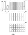
- FIG. 8 is a schematic block diagram illustrating an example of a suboptimally configured memory array 706 .
- a counting criterion of greater than is assumed, which is equivalent to less than in terms of the performance class number, and a nominal threshold percentage of 50% is assumed.
- the overall performance of the array 706 is of performance class is two, because the inherent performance capability of memory device 802 is of performance class two, and the second tier 712 - 2 is populated by a memory device 804 .
- the qualified count is five, because five of the memory devices 500 are of performance class one, which is less than the performance class two of the array 706 .
- the unqualified count is six, being the total number of memory devices 500 in the array 706 .
- the threshold is three, being 50% of six. Thus the qualified count is greater than the threshold, causing the memory configuration warning to be issued.
- FIG. 9 is a schematic block diagram of an optimized reconfiguration of the suboptimally configured memory array 706 .
- the memory device 802 of performance class two has been replaced with a memory device 902 of performance class one.
- the memory device 804 has been moved from slot 708 - 2 of the second tier 712 - 2 to slot 708 - 1 of the first tier 712 - 1 .
- the overall performance of the array 706 is now of performance class one.
- the qualified count is now zero, because none of the memory devices 500 are of a performance class less than that of the array 706 .
- the qualified count is less than the threshold, causing the memory configuration warning to no longer be issued.
- FIG. 10 is a schematic flow chart diagram illustrating one embodiment of a method for determining overall performance of a memory array 706 as may be performed by a classification module 402 in accordance with the present invention.
- the method 1000 starts 1002 and the overall performance class of the array 706 , the unqualified count, and the quantity of memory devices 500 populating a subset or channel 710 are initialized 1004 to one, zero, and zero, respectively.
- the memory devices 500 are then examined in turn, classifying 1006 the individual performance capability of the next memory device, and the unqualified count and the quantity are both incremented 1008 . If the memory device performance class representing the individual performance capability of the memory device 500 is greater than 1010 the overall performance class, then the overall performance class is set equal 1012 to the memory device performance class.
- the overall performance class is set equal 1016 to the quantity. If the memory device 500 is not the last 1018 device in the subset, then the next memory device 500 is classified 1006 and the ensuing steps are repeated. If the subset is not the last 1020 subset in the array 706 , then the next subset is examined in turn, reinitializing 1022 the quantity to zero, classifying 1006 the next memory device 500 , and repeating the ensuing steps as before.
- the overall performance class has now been determined as the maximum of the memory device performance class of any individual memory device 500 and the quantity of memory devices 500 in any subset, the unqualified count has been determined as the total count of memory devices 500 comprising the array 706 , and the method 1000 ends 1024 .
- FIG. 11 is a schematic flow chart diagram illustrating one embodiment of a method for memory configuration analysis as may be performed by a counting module 404 and a comparison module 406 in accordance with the present invention.
- the method 1100 starts 1102 and the predetermined threshold and the qualified count are initialized 1104 to a predetermined percentage of the unqualified count, as determined by the method 1000 , and to zero, respectively.
- the memory devices 500 are then examined in turn, classifying 1106 the individual performance capability of the next memory device. If the memory device performance class representing the individual performance capability of the memory device 500 is less than 1108 the overall performance class, as determined by the method 1000 , then the qualified count is incremented 1110 .
- a selected action is taken such as issuing 1114 a memory configuration warning, and the method 1100 ends 1116 . If the memory device 500 is not the last 1118 device in the array 706 , then the next memory device 500 is classified 1106 and the ensuing steps are repeated. Otherwise, no selected action is taken and the method 1100 ends 1120 .
Abstract
Description
Claims (25)
Priority Applications (1)
| Application Number | Priority Date | Filing Date | Title |
|---|---|---|---|
| US12/410,300 US8606545B2 (en) | 2009-03-24 | 2009-03-24 | Apparatus, system, and method for memory configuration analysis |
Applications Claiming Priority (1)
| Application Number | Priority Date | Filing Date | Title |
|---|---|---|---|
| US12/410,300 US8606545B2 (en) | 2009-03-24 | 2009-03-24 | Apparatus, system, and method for memory configuration analysis |
Publications (2)
| Publication Number | Publication Date |
|---|---|
| US20100250197A1 US20100250197A1 (en) | 2010-09-30 |
| US8606545B2 true US8606545B2 (en) | 2013-12-10 |
Family
ID=42785320
Family Applications (1)
| Application Number | Title | Priority Date | Filing Date |
|---|---|---|---|
| US12/410,300 Active 2030-12-26 US8606545B2 (en) | 2009-03-24 | 2009-03-24 | Apparatus, system, and method for memory configuration analysis |
Country Status (1)
| Country | Link |
|---|---|
| US (1) | US8606545B2 (en) |
Cited By (1)
| Publication number | Priority date | Publication date | Assignee | Title |
|---|---|---|---|---|
| US11409515B2 (en) | 2019-02-01 | 2022-08-09 | Hewlett-Packard Development Company, L.P. | Upgrade determinations of devices based on telemetry data |
Families Citing this family (1)
| Publication number | Priority date | Publication date | Assignee | Title |
|---|---|---|---|---|
| TWI420309B (en) * | 2010-11-12 | 2013-12-21 | Inventec Corp | Method for setting memory address space |
Citations (6)
| Publication number | Priority date | Publication date | Assignee | Title |
|---|---|---|---|---|
| US5321840A (en) * | 1988-05-05 | 1994-06-14 | Transaction Technology, Inc. | Distributed-intelligence computer system including remotely reconfigurable, telephone-type user terminal |
| US5594879A (en) * | 1993-10-29 | 1997-01-14 | Compaq Computer Corporation | Method of and apparatus for arbitrarily disabling under processor control individual slots on a computer bus |
| US7072728B2 (en) * | 1999-11-19 | 2006-07-04 | Dell Products L.P. | Method for assembling hardware components in a computer system |
| US7127622B2 (en) * | 2003-03-04 | 2006-10-24 | Micron Technology, Inc. | Memory subsystem voltage control and method |
| US7424577B2 (en) * | 2005-08-26 | 2008-09-09 | Network Appliance, Inc. | Dynamic optimization of cache memory |
| US7506297B2 (en) * | 2004-06-15 | 2009-03-17 | University Of North Carolina At Charlotte | Methodology for scheduling, partitioning and mapping computational tasks onto scalable, high performance, hybrid FPGA networks |
-
2009
- 2009-03-24 US US12/410,300 patent/US8606545B2/en active Active
Patent Citations (6)
| Publication number | Priority date | Publication date | Assignee | Title |
|---|---|---|---|---|
| US5321840A (en) * | 1988-05-05 | 1994-06-14 | Transaction Technology, Inc. | Distributed-intelligence computer system including remotely reconfigurable, telephone-type user terminal |
| US5594879A (en) * | 1993-10-29 | 1997-01-14 | Compaq Computer Corporation | Method of and apparatus for arbitrarily disabling under processor control individual slots on a computer bus |
| US7072728B2 (en) * | 1999-11-19 | 2006-07-04 | Dell Products L.P. | Method for assembling hardware components in a computer system |
| US7127622B2 (en) * | 2003-03-04 | 2006-10-24 | Micron Technology, Inc. | Memory subsystem voltage control and method |
| US7506297B2 (en) * | 2004-06-15 | 2009-03-17 | University Of North Carolina At Charlotte | Methodology for scheduling, partitioning and mapping computational tasks onto scalable, high performance, hybrid FPGA networks |
| US7424577B2 (en) * | 2005-08-26 | 2008-09-09 | Network Appliance, Inc. | Dynamic optimization of cache memory |
Cited By (1)
| Publication number | Priority date | Publication date | Assignee | Title |
|---|---|---|---|---|
| US11409515B2 (en) | 2019-02-01 | 2022-08-09 | Hewlett-Packard Development Company, L.P. | Upgrade determinations of devices based on telemetry data |
Also Published As
| Publication number | Publication date |
|---|---|
| US20100250197A1 (en) | 2010-09-30 |
Similar Documents
| Publication | Publication Date | Title |
|---|---|---|
| US20070043923A1 (en) | Apparatus, system, and method for modifying data storage configuration | |
| US10656833B2 (en) | Hybrid memory drives, computer system, and related method for operating a multi-mode hybrid drive | |
| US10289339B2 (en) | System and method for storing modified data to an NVDIMM during a save operation | |
| US20230017171A1 (en) | Identification and Classification of Write Stream Priority | |
| US20140149807A1 (en) | Controller For Reading Data From Non-Volatile Memory | |
| US10657052B2 (en) | Information handling system with priority based cache flushing of flash dual in-line memory module pool | |
| US20140052894A1 (en) | Memory controller for memory with mixed cell array and method of controlling the memory | |
| CN113253916A (en) | Delay and throughput centric reconfigurable storage device | |
| US10572183B2 (en) | Power efficient retraining of memory accesses | |
| TW201303870A (en) | Effective utilization of flash interface | |
| US8606545B2 (en) | Apparatus, system, and method for memory configuration analysis | |
| US20200082241A1 (en) | Cognitive storage device | |
| US8627003B2 (en) | Apparatus, system, and method for memory upgrade path optimization | |
| US20240127870A1 (en) | Configuring a host interface of a memory device based on mode of operation | |
| US11681807B2 (en) | Information handling system with mechanism for reporting status of persistent memory firmware update | |
| US10635311B2 (en) | Information handling system with reduced reset during dual in-line memory module goal reconfiguration | |
| US11392470B2 (en) | Information handling system to allow system boot when an amount of installed memory exceeds processor limit | |
| US11487638B2 (en) | Computer program product and method and apparatus for controlling access to flash memory card | |
| US20200242067A1 (en) | System and Method for I/O Aware Processor Configuration | |
| Li et al. | A learning-based approach towards automated tuning of ssd configurations | |
| US20170228404A1 (en) | Information processing apparatus, processing apparatus, data search method | |
| EP2757481A1 (en) | Caching method and caching system using dual disks | |
| US11422702B2 (en) | Managing utilization of storage class memory (SCM) resources | |
| CN113448884A (en) | Parallel overlap management of commands with overlapping ranges | |
| US7302521B2 (en) | Method and computer program product for combining resources of multiple BIOS ROMS and managing them as a single entity |
Legal Events
| Date | Code | Title | Description |
|---|---|---|---|
| AS | Assignment |
Owner name: LENOVO (SINGAPORE) PTE. LTD., SINGAPORE Free format text: ASSIGNMENT OF ASSIGNORS INTEREST;ASSIGNORS:CROMER, DARYL;FRAME, DONALD R.;METTLER, MICHAEL SCOTT;AND OTHERS;REEL/FRAME:022593/0428 Effective date: 20090324 |
|
| STCF | Information on status: patent grant |
Free format text: PATENTED CASE |
|
| AS | Assignment |
Owner name: LENOVO PC INTERNATIONAL, HONG KONG Free format text: NUNC PRO TUNC ASSIGNMENT;ASSIGNOR:LENOVO (SINGAPORE) PTE LTD.;REEL/FRAME:037211/0283 Effective date: 20140101 |
|
| FPAY | Fee payment |
Year of fee payment: 4 |
|
| AS | Assignment |
Owner name: LENOVO PC INTERNATIONAL, HONG KONG Free format text: ASSIGNMENT OF ASSIGNORS INTEREST;ASSIGNOR:LENOVO (SINGAPORE) PTE. LTD.;REEL/FRAME:049678/0855 Effective date: 20140101 |
|
| MAFP | Maintenance fee payment |
Free format text: PAYMENT OF MAINTENANCE FEE, 8TH YEAR, LARGE ENTITY (ORIGINAL EVENT CODE: M1552); ENTITY STATUS OF PATENT OWNER: LARGE ENTITY Year of fee payment: 8 |