US8604504B2 - Organic light-emitting element - Google Patents
Organic light-emitting element Download PDFInfo
- Publication number
- US8604504B2 US8604504B2 US13/637,138 US201113637138A US8604504B2 US 8604504 B2 US8604504 B2 US 8604504B2 US 201113637138 A US201113637138 A US 201113637138A US 8604504 B2 US8604504 B2 US 8604504B2
- Authority
- US
- United States
- Prior art keywords
- light
- transparent substrate
- polarized light
- organic light
- refractive index
- Prior art date
- Legal status (The legal status is an assumption and is not a legal conclusion. Google has not performed a legal analysis and makes no representation as to the accuracy of the status listed.)
- Active
Links
- 239000000758 substrate Substances 0.000 claims abstract description 140
- 238000000605 extraction Methods 0.000 claims abstract description 28
- 230000005684 electric field Effects 0.000 claims abstract description 17
- 230000010355 oscillation Effects 0.000 claims abstract description 16
- 230000003287 optical effect Effects 0.000 claims description 8
- 239000011112 polyethylene naphthalate Substances 0.000 claims description 5
- 229920003207 poly(ethylene-2,6-naphthalate) Polymers 0.000 claims description 4
- -1 polyethylene naphthalate Polymers 0.000 claims description 3
- 229920000139 polyethylene terephthalate Polymers 0.000 claims description 3
- 239000005020 polyethylene terephthalate Substances 0.000 claims description 3
- 239000004793 Polystyrene Substances 0.000 claims description 2
- 239000013078 crystal Substances 0.000 claims description 2
- 229920000515 polycarbonate Polymers 0.000 claims description 2
- 239000004417 polycarbonate Substances 0.000 claims description 2
- 239000004800 polyvinyl chloride Substances 0.000 claims description 2
- 229920002223 polystyrene Polymers 0.000 claims 1
- 229920000915 polyvinyl chloride Polymers 0.000 claims 1
- 239000010410 layer Substances 0.000 description 125
- 230000000052 comparative effect Effects 0.000 description 26
- 239000000463 material Substances 0.000 description 26
- 238000000034 method Methods 0.000 description 20
- 238000002347 injection Methods 0.000 description 11
- 239000007924 injection Substances 0.000 description 11
- 230000000903 blocking effect Effects 0.000 description 10
- 230000005525 hole transport Effects 0.000 description 9
- 229910052751 metal Inorganic materials 0.000 description 6
- 239000002184 metal Substances 0.000 description 6
- 230000006872 improvement Effects 0.000 description 5
- 238000010586 diagram Methods 0.000 description 4
- 238000005286 illumination Methods 0.000 description 4
- PQXKHYXIUOZZFA-UHFFFAOYSA-M lithium fluoride Chemical compound [Li+].[F-] PQXKHYXIUOZZFA-UHFFFAOYSA-M 0.000 description 4
- 238000004519 manufacturing process Methods 0.000 description 4
- ZWEHNKRNPOVVGH-UHFFFAOYSA-N 2-Butanone Chemical compound CCC(C)=O ZWEHNKRNPOVVGH-UHFFFAOYSA-N 0.000 description 3
- IAZDPXIOMUYVGZ-UHFFFAOYSA-N Dimethylsulphoxide Chemical compound CS(C)=O IAZDPXIOMUYVGZ-UHFFFAOYSA-N 0.000 description 3
- XEKOWRVHYACXOJ-UHFFFAOYSA-N Ethyl acetate Chemical compound CCOC(C)=O XEKOWRVHYACXOJ-UHFFFAOYSA-N 0.000 description 3
- YXFVVABEGXRONW-UHFFFAOYSA-N Toluene Chemical compound CC1=CC=CC=C1 YXFVVABEGXRONW-UHFFFAOYSA-N 0.000 description 3
- 239000006185 dispersion Substances 0.000 description 3
- 230000000694 effects Effects 0.000 description 3
- 239000010408 film Substances 0.000 description 3
- 150000002894 organic compounds Chemical class 0.000 description 3
- 239000011347 resin Substances 0.000 description 3
- 229920005989 resin Polymers 0.000 description 3
- 238000004544 sputter deposition Methods 0.000 description 3
- 239000010409 thin film Substances 0.000 description 3
- 238000007740 vapor deposition Methods 0.000 description 3
- PXHVJJICTQNCMI-UHFFFAOYSA-N Nickel Chemical compound [Ni] PXHVJJICTQNCMI-UHFFFAOYSA-N 0.000 description 2
- VYPSYNLAJGMNEJ-UHFFFAOYSA-N Silicium dioxide Chemical compound O=[Si]=O VYPSYNLAJGMNEJ-UHFFFAOYSA-N 0.000 description 2
- 229910052782 aluminium Inorganic materials 0.000 description 2
- XAGFODPZIPBFFR-UHFFFAOYSA-N aluminium Chemical compound [Al] XAGFODPZIPBFFR-UHFFFAOYSA-N 0.000 description 2
- 230000008901 benefit Effects 0.000 description 2
- 230000015572 biosynthetic process Effects 0.000 description 2
- JHIVVAPYMSGYDF-UHFFFAOYSA-N cyclohexanone Chemical compound O=C1CCCCC1 JHIVVAPYMSGYDF-UHFFFAOYSA-N 0.000 description 2
- NNBZCPXTIHJBJL-UHFFFAOYSA-N decalin Chemical compound C1CCCC2CCCCC21 NNBZCPXTIHJBJL-UHFFFAOYSA-N 0.000 description 2
- SNRUBQQJIBEYMU-UHFFFAOYSA-N dodecane Chemical compound CCCCCCCCCCCC SNRUBQQJIBEYMU-UHFFFAOYSA-N 0.000 description 2
- 238000005401 electroluminescence Methods 0.000 description 2
- 239000011521 glass Substances 0.000 description 2
- 239000004973 liquid crystal related substance Substances 0.000 description 2
- 238000005259 measurement Methods 0.000 description 2
- 230000035699 permeability Effects 0.000 description 2
- 230000008569 process Effects 0.000 description 2
- 230000009467 reduction Effects 0.000 description 2
- 150000003839 salts Chemical class 0.000 description 2
- 239000002356 single layer Substances 0.000 description 2
- 238000004528 spin coating Methods 0.000 description 2
- XOLBLPGZBRYERU-UHFFFAOYSA-N tin dioxide Chemical compound O=[Sn]=O XOLBLPGZBRYERU-UHFFFAOYSA-N 0.000 description 2
- 239000012780 transparent material Substances 0.000 description 2
- OCJBOOLMMGQPQU-UHFFFAOYSA-N 1,4-dichlorobenzene Chemical compound ClC1=CC=C(Cl)C=C1 OCJBOOLMMGQPQU-UHFFFAOYSA-N 0.000 description 1
- OYPRJOBELJOOCE-UHFFFAOYSA-N Calcium Chemical compound [Ca] OYPRJOBELJOOCE-UHFFFAOYSA-N 0.000 description 1
- XDTMQSROBMDMFD-UHFFFAOYSA-N Cyclohexane Chemical compound C1CCCCC1 XDTMQSROBMDMFD-UHFFFAOYSA-N 0.000 description 1
- DGAQECJNVWCQMB-PUAWFVPOSA-M Ilexoside XXIX Chemical compound C[C@@H]1CC[C@@]2(CC[C@@]3(C(=CC[C@H]4[C@]3(CC[C@@H]5[C@@]4(CC[C@@H](C5(C)C)OS(=O)(=O)[O-])C)C)[C@@H]2[C@]1(C)O)C)C(=O)O[C@H]6[C@@H]([C@H]([C@@H]([C@H](O6)CO)O)O)O.[Na+] DGAQECJNVWCQMB-PUAWFVPOSA-M 0.000 description 1
- CTQNGGLPUBDAKN-UHFFFAOYSA-N O-Xylene Chemical compound CC1=CC=CC=C1C CTQNGGLPUBDAKN-UHFFFAOYSA-N 0.000 description 1
- BQCADISMDOOEFD-UHFFFAOYSA-N Silver Chemical compound [Ag] BQCADISMDOOEFD-UHFFFAOYSA-N 0.000 description 1
- RTAQQCXQSZGOHL-UHFFFAOYSA-N Titanium Chemical compound [Ti] RTAQQCXQSZGOHL-UHFFFAOYSA-N 0.000 description 1
- 150000001338 aliphatic hydrocarbons Chemical class 0.000 description 1
- 239000000956 alloy Substances 0.000 description 1
- 229910045601 alloy Inorganic materials 0.000 description 1
- PNEYBMLMFCGWSK-UHFFFAOYSA-N aluminium oxide Inorganic materials [O-2].[O-2].[O-2].[Al+3].[Al+3] PNEYBMLMFCGWSK-UHFFFAOYSA-N 0.000 description 1
- 238000000149 argon plasma sintering Methods 0.000 description 1
- 150000004945 aromatic hydrocarbons Chemical class 0.000 description 1
- QVGXLLKOCUKJST-UHFFFAOYSA-N atomic oxygen Chemical compound [O] QVGXLLKOCUKJST-UHFFFAOYSA-N 0.000 description 1
- 230000004888 barrier function Effects 0.000 description 1
- 229910052791 calcium Inorganic materials 0.000 description 1
- 239000011575 calcium Substances 0.000 description 1
- 238000005266 casting Methods 0.000 description 1
- 230000015556 catabolic process Effects 0.000 description 1
- 238000000576 coating method Methods 0.000 description 1
- 238000004891 communication Methods 0.000 description 1
- 150000001875 compounds Chemical class 0.000 description 1
- HHNHBFLGXIUXCM-GFCCVEGCSA-N cyclohexylbenzene Chemical compound [CH]1CCCC[C@@H]1C1=CC=CC=C1 HHNHBFLGXIUXCM-GFCCVEGCSA-N 0.000 description 1
- 238000006731 degradation reaction Methods 0.000 description 1
- 230000006866 deterioration Effects 0.000 description 1
- 229940117389 dichlorobenzene Drugs 0.000 description 1
- 150000002194 fatty esters Chemical class 0.000 description 1
- 239000007850 fluorescent dye Substances 0.000 description 1
- 239000003574 free electron Substances 0.000 description 1
- 239000007789 gas Substances 0.000 description 1
- 150000008282 halocarbons Chemical class 0.000 description 1
- AMGQUBHHOARCQH-UHFFFAOYSA-N indium;oxotin Chemical compound [In].[Sn]=O AMGQUBHHOARCQH-UHFFFAOYSA-N 0.000 description 1
- 150000002576 ketones Chemical class 0.000 description 1
- 239000007788 liquid Substances 0.000 description 1
- AUHZEENZYGFFBQ-UHFFFAOYSA-N mesitylene Substances CC1=CC(C)=CC(C)=C1 AUHZEENZYGFFBQ-UHFFFAOYSA-N 0.000 description 1
- 125000001827 mesitylenyl group Chemical group [H]C1=C(C(*)=C(C([H])=C1C([H])([H])[H])C([H])([H])[H])C([H])([H])[H] 0.000 description 1
- 239000007769 metal material Substances 0.000 description 1
- 239000004005 microsphere Substances 0.000 description 1
- 229910052759 nickel Inorganic materials 0.000 description 1
- 239000003960 organic solvent Substances 0.000 description 1
- 239000001301 oxygen Substances 0.000 description 1
- 229910052760 oxygen Inorganic materials 0.000 description 1
- 238000005215 recombination Methods 0.000 description 1
- 230000006798 recombination Effects 0.000 description 1
- 238000002310 reflectometry Methods 0.000 description 1
- 230000004044 response Effects 0.000 description 1
- 238000010008 shearing Methods 0.000 description 1
- 239000000377 silicon dioxide Substances 0.000 description 1
- 229910052709 silver Inorganic materials 0.000 description 1
- 239000004332 silver Substances 0.000 description 1
- 229910052708 sodium Inorganic materials 0.000 description 1
- 239000011734 sodium Substances 0.000 description 1
- 239000000243 solution Substances 0.000 description 1
- 238000003860 storage Methods 0.000 description 1
- 230000003746 surface roughness Effects 0.000 description 1
- 229910052719 titanium Inorganic materials 0.000 description 1
- 239000010936 titanium Substances 0.000 description 1
- 238000002834 transmittance Methods 0.000 description 1
- 239000003981 vehicle Substances 0.000 description 1
- PXXNTAGJWPJAGM-UHFFFAOYSA-N vertaline Natural products C1C2C=3C=C(OC)C(OC)=CC=3OC(C=C3)=CC=C3CCC(=O)OC1CC1N2CCCC1 PXXNTAGJWPJAGM-UHFFFAOYSA-N 0.000 description 1
- 239000008096 xylene Substances 0.000 description 1
Images


Classifications
-
- H—ELECTRICITY
- H05—ELECTRIC TECHNIQUES NOT OTHERWISE PROVIDED FOR
- H05B—ELECTRIC HEATING; ELECTRIC LIGHT SOURCES NOT OTHERWISE PROVIDED FOR; CIRCUIT ARRANGEMENTS FOR ELECTRIC LIGHT SOURCES, IN GENERAL
- H05B33/00—Electroluminescent light sources
- H05B33/12—Light sources with substantially two-dimensional radiating surfaces
- H05B33/14—Light sources with substantially two-dimensional radiating surfaces characterised by the chemical or physical composition or the arrangement of the electroluminescent material, or by the simultaneous addition of the electroluminescent material in or onto the light source
- H05B33/145—Arrangements of the electroluminescent material
-
- H—ELECTRICITY
- H10—SEMICONDUCTOR DEVICES; ELECTRIC SOLID-STATE DEVICES NOT OTHERWISE PROVIDED FOR
- H10K—ORGANIC ELECTRIC SOLID-STATE DEVICES
- H10K50/00—Organic light-emitting devices
- H10K50/80—Constructional details
- H10K50/85—Arrangements for extracting light from the devices
-
- H—ELECTRICITY
- H10—SEMICONDUCTOR DEVICES; ELECTRIC SOLID-STATE DEVICES NOT OTHERWISE PROVIDED FOR
- H10K—ORGANIC ELECTRIC SOLID-STATE DEVICES
- H10K50/00—Organic light-emitting devices
- H10K50/80—Constructional details
- H10K50/85—Arrangements for extracting light from the devices
- H10K50/858—Arrangements for extracting light from the devices comprising refractive means, e.g. lenses
-
- H—ELECTRICITY
- H10—SEMICONDUCTOR DEVICES; ELECTRIC SOLID-STATE DEVICES NOT OTHERWISE PROVIDED FOR
- H10K—ORGANIC ELECTRIC SOLID-STATE DEVICES
- H10K59/00—Integrated devices, or assemblies of multiple devices, comprising at least one organic light-emitting element covered by group H10K50/00
- H10K59/80—Constructional details
- H10K59/875—Arrangements for extracting light from the devices
- H10K59/879—Arrangements for extracting light from the devices comprising refractive means, e.g. lenses
-
- H—ELECTRICITY
- H10—SEMICONDUCTOR DEVICES; ELECTRIC SOLID-STATE DEVICES NOT OTHERWISE PROVIDED FOR
- H10K—ORGANIC ELECTRIC SOLID-STATE DEVICES
- H10K50/00—Organic light-emitting devices
- H10K50/80—Constructional details
- H10K50/85—Arrangements for extracting light from the devices
- H10K50/854—Arrangements for extracting light from the devices comprising scattering means
-
- H—ELECTRICITY
- H10—SEMICONDUCTOR DEVICES; ELECTRIC SOLID-STATE DEVICES NOT OTHERWISE PROVIDED FOR
- H10K—ORGANIC ELECTRIC SOLID-STATE DEVICES
- H10K59/00—Integrated devices, or assemblies of multiple devices, comprising at least one organic light-emitting element covered by group H10K50/00
- H10K59/80—Constructional details
- H10K59/875—Arrangements for extracting light from the devices
- H10K59/877—Arrangements for extracting light from the devices comprising scattering means
Definitions
- the present invention relates to an organic light-emitting element including an organic light-emitting layer, a transparent substrate, and a transparent electrode that is provided between the organic light-emitting layer and the transparent substrate, in which a surface of the transparent substrate on the opposite side to the transparent electrode is used as a light extraction surface.
- An organic light-emitting element can provide a high luminance using low power and is excellent in terms of visibility, a response speed, a service life, and power consumption.
- the light use efficiency thereof is on the order of 20%, and hence there is a large loss in an organic light-emitting element.
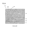
- FIG. 9 is a schematic sectional view of a conventional organic light-emitting element.
- An organic light-emitting element 100 is formed by stacking, in order from a lower layer in the figure, a metal electrode 101 , an organic light-emitting layer 102 , a transparent electrode 103 , and a transparent substrate 104 .
- arrows 110 a to 110 e represent characteristic ones of light rays generated from the organic light-emitting layer 102 .
- the light ray 110 a is a light ray in a perpendicular direction to the organic light-emitting layer 102 that is a light-emitting plane, which is transmitted through the transparent substrate 104 to be extracted to a light extraction side (air side).
- the light ray 110 b is a light ray that has entered an interface between the transparent substrate 104 and the air at a shallow angle not more than a critical angle and is refracted at the interface between the transparent substrate 104 and the air to be extracted to the light extraction side.
- the light ray 110 c is a light ray that has entered the interface between the transparent substrate 104 and the air at an angle deeper than the critical angle and is totally reflected off the interface between the transparent substrate 104 and the air, thus failing to be extracted to the light extraction side.
- a loss attributable to this is referred to as a substrate loss, and due thereto, there is typically a loss on the order of 20%.
- the light ray 110 d is a light ray satisfying a resonance condition among light rays that have entered an interface between the transparent electrode 103 and the transparent substrate 104 at an angle deeper than a critical angle.
- the light ray 110 d is totally reflected off the interface between the transparent electrode 103 and the transparent substrate 104 , which establishes a waveguide mode in which the light ray 110 d is trapped inside the organic light-emitting layer 102 and the transparent electrode 103 .
- a loss attributable to this is referred to as a waveguide loss, and due thereto, there is typically a loss on the order of 20 to 25%.
- the light ray 110 e is a light ray that enters the metal electrode 101 to interact with a free electron in the metal electrode 101 , which establishes a plasmon mode that is one form of the waveguide mode, in which the light ray 110 e is trapped in the vicinity of a surface of the metal electrode 101 .
- a loss attributable to this is referred to as a plasmon loss, and due thereto, there is typically a loss on the order of 30 to 40%.
- the conventional organic light-emitting element 100 there are a substrate loss, a waveguide loss, and a plasmon loss, and hence it has been sought to reduce these losses so as to extract a maximum possible amount of light.
- Patent Document 1 discloses an organic EL (electro luminescence) device in which a light scattering portion constituted by a lens sheet is provided on a light extraction surface side.
- Patent Document 2 discloses a substrate for a light-emitting device and a light-emitting device.
- the substrate for a light-emitting device disclosed therein is composed of a high refractive index convexo-concave layer having a refractive index of not less than 1.6 and an average surface roughness of not less than 10 nm, which is provided on a surface of the substrate at least on one side thereof, and one or more base material layers each having a refractive index of not less than 1.55, and is used on a light-emitting surface side of the light-emitting device.
- Patent Documents 1 and 2 are both intended to reduce a substrate loss by changing the shape of an interface between a transparent substrate and the air so as to achieve an improvement in light use efficiency.
- Patent Documents 1 and 2 disclose no measures to reduce a waveguide loss and a plasmon loss. Thus, by reducing a waveguide loss and a plasmon loss, it is possible to achieve a further improvement in light use efficiency.
- an object of the present invention to provide an organic light-emitting element that is reduced in waveguide loss and thus achieves an improvement in light use efficiency.
- the present invention provides an organic light-emitting element including: an organic light-emitting layer; a transparent substrate; and a transparent electrode that is provided between the organic light-emitting layer and the transparent substrate, in which a surface of the transparent substrate on the opposite side to the transparent electrode is used as a light extraction surface.
- the transparent substrate has birefringence, and where polarized light having an electric field oscillation direction parallel to a stacking plane of the organic light-emitting layer is defined as S-polarized light, and polarized light having an electric field oscillation direction included in a plane that includes a vector in a travel direction of the light and is perpendicular to the stacking plane of the organic light-emitting layer is defined as P-polarized light, the refractive index of the transparent substrate for the P-polarized light is smaller than that of the transparent substrate for the S-polarized light.
- the transparent substrate has birefringence, and thus a waveguide loss can be reduced, so that an improvement in light use efficiency can be achieved.
- FIG. 1 A schematic sectional view of an organic light-emitting element in an embodiment of the present invention.
- FIG. 2 A graph showing whether or not various modes exist in a case where, in an organic light-emitting element using a transparent electrode having a refractive index of 1.8 and a transparent substrate having a refractive index of 1.75, the total thickness of an organic light-emitting layer and the transparent electrode is made to vary.
- FIG. 3 A graph showing whether or not the various modes exist in a case where, in an organic light-emitting element using a transparent electrode having a refractive index of 1.8 and a transparent substrate having a refractive index of 1.5, the total thickness of an organic light-emitting layer and the transparent electrode is made to vary.
- FIG. 4 A diagram in which respective features of Examples 1 and 2 and Comparative Examples 1 and 2 are summarized.
- FIG. 5 A schematic sectional view of an organic light-emitting element in another embodiment of the present invention.
- FIG. 6 A diagram showing values of light extraction efficiency of S-polarized light, P-polarized light, and a total of the S-polarized light and the P-polarized light in a case where an organic light-emitting element of Example 1 is provided with a light angle changing element made of each of isotropic materials varying in refractive index.
- FIG. 7 A diagram in which the values shown in FIG. 6 are plotted in the form of a graph.
- FIG. 8 A schematic sectional view of an organic light-emitting element in still another embodiment of the present invention.
- FIG. 9 A schematic sectional view of a conventional organic light-emitting element.
- FIG. 1 is a schematic sectional view of an organic light-emitting element in an embodiment of the present invention.
- An organic light-emitting element 10 is formed by stacking, in order from a lower layer in the figure, a rear surface electrode 11 , an organic light-emitting layer 12 , a transparent electrode 13 , and a transparent substrate 14 .
- the organic light-emitting element 10 is of a bottom emission type in which a surface of the transparent substrate 14 on the opposite side to the transparent electrode 13 is used as a light extraction surface.
- a lateral direction in the plane of the figure is defined as an X direction, a direction perpendicular to the plane of the figure as a Y direction, and a vertical direction in the plane of the figure (a stacking direction in which the respective layers are stacked) as a Z direction.
- the rear surface electrode 11 acts as an anode or a cathode and also as a mirror that reflects light to the side of the transparent substrate 14 , and as a material thereof, for example, a metal material having a reflectivity of not less than 60% such as aluminum, silver, nickel, titanium, sodium, or calcium or an alloy containing any of these materials can be used.
- the organic light-emitting layer 12 is constituted by a single or multiple organic compound or complex layers including a luminous layer and is composed of, for example, a positive hole transport layer in contact with the anode, the luminous layer made of a luminous material, and an electron transport layer in contact with the cathode, and the thickness thereof is several nm to several hundreds of nm.
- the organic light-emitting layer 12 has a refractive index in the neighborhood of 1.8.
- a lithium fluoride layer, a layer of an inorganic metal salt, a layer containing lithium fluoride or an inorganic metal salt, or the like may be formed at an arbitrary position.
- the luminous layer is made of at least one type of luminous material, and as the luminous material, a fluorescent compound, a phosphorescent compound, or the like can be used.
- any of configurations (i) to (v) below, which includes the above-described configuration, can be adopted.
- the positive hole transport layer is made of a material having a function of transporting a positive hole and subsumes, in a broader sense, the positive hole injection layer and the electron blocking layer.
- the positive hole transport layer can be provided in a single or multiple layers.
- the electron transport layer is made of a material having a function of transporting an electron and subsumes, in a broader sense, the electron injection layer and the positive hole blocking layer.
- the electron transport layer can be provided in a single or multiple layers.
- the positive hole blocking layer in a broader sense, has the function of the electron transport layer and is made of a positive hole blocking material that, while having a function of transporting an electron, is significantly poor in capability of transporting a positive hole, thus blocking a positive hole while transporting an electron, so that the probability of recombination between an electron and a positive hole can be improved.
- the positive hole injection layer and the electron injection layer are layers that are each provided between an electrode and a luminous layer so that a decrease in driving voltage and an improvement in emission luminance can be achieved.
- the transparent electrode 13 is a counter electrode to the rear surface electrode 11 , and as a material thereof, for example, an electrically conductive transparent material having a light transmittance of not less than 40% such as CuI, indium tin oxide (ITO), SnO 2 , or ZnO can be used.
- the transparent electrode 13 has a refractive index in the neighborhood of 1.8, which is equal to that of the organic light-emitting layer 12 .
- the transparent substrate 14 is made of a transparent material having a birefringence and has a thickness of, for example, 0.1 to 1 mm. As will be described later, preferably, a birefringence property thereof is such that its refractive index for P-polarized light is smaller than that for S-polarized light. Furthermore, preferably, the transparent substrate 14 is uniaxial and has an optical axis perpendicular (Z direction) to the organic light-emitting layer 12 and to a stacking plane (X-Y plane) of the transparent substrate 14 . In this case, the refractive index in the X direction is equal to that in the Y direction, and the refractive index in the Z direction is different from those in the X direction and in the Y direction.
- the transparent substrate 14 may be biaxial as long as its refractive index for P-polarized light is smaller than that for S-polarized light as described above.
- the transparent substrate 14 has a refractive index in a range in the neighborhood of 1.5 to 1.8.
- the transparent substrate 14 As a material of the transparent substrate 14 , for example, resin such as polyethylene naphthalate (PEN), polyethylene terephthalate (PET), polycarbonate (PC), polystyrene (PS), or polyvinyl chloride (PVC), or crystal can be used. Preferably used is a resin film that can impart flexibility to the organic light-emitting element. Using a flexible film-shaped base material to form the transparent substrate 14 allows a planar light source to be curved and thus can achieve light emission toward different directions.
- resin such as polyethylene naphthalate (PEN), polyethylene terephthalate (PET), polycarbonate (PC), polystyrene (PS), or polyvinyl chloride (PVC), or crystal
- PEN polyethylene naphthalate
- PET polyethylene terephthalate
- PC polycarbonate
- PS polystyrene
- PVC polyvinyl chloride
- the transparent electrode 13 On the transparent substrate 14 , the transparent electrode 13 , the organic light-emitting layer 12 , and the rear surface electrode 11 are stacked, and electrode portions are formed by exposing the transparent electrode 13 at one end and by exposing the rear surface electrode 11 at the other end and are connected to power source wiring lines (not shown) of a power source portion (not shown), respectively. Then, a predetermined direct current voltage is applied to the organic light-emitting layer 12 so as to cause light emission.
- the organic compound used to form the organic light-emitting element 10 is subject to degradation due to moisture or oxygen in the air, preferably, the organic light-emitting element 10 is sealed with an anti-moisture permeability layer (gas barrier layer) so as to be used in a state shielded from the outside atmosphere.
- the anti-moisture permeability layer can be formed by, for example, a radio frequency sputtering method.
- a hard coat layer, an undercoat layer, or the like may be provided as required.
- the following describes a method for manufacturing an element having the following configuration: transparent substrate/anode/positive hole injection layer/positive hole transport layer/luminous layer/positive hole blocking layer/electron transport layer/electron injection layer/cathode.
- a thin film of a material for an anode is formed in a thickness of not more than 1 ⁇ m, preferably, a thickness of 10 nm to 200 nm by a method such as vapor deposition or sputtering to prepare an anode.
- organic compound thin films such as the positive hole injection layer, the positive hole transport layer, the luminous layer, the positive hole blocking layer, the electron transport layer, the electron injection layer are formed thereon.
- Usable methods for forming these layers include a vapor deposition method, a wet process (a spin coating method, a casting method, an ink jet method, a printing method), and the like, and from a viewpoint such as of easily obtaining a homogeneous film and hardly generating a pinhole, preferable is film formation by a coating method such as the spin coating method, the ink-jet method, or the printing method.
- liquid medium in which the organic light-emitting layer 12 is dissolved or dispersed for example, ketones such as methyl ethyl ketone and cyclohexanone, fatty esters such as ethyl acetate, halogenated hydrocarbons such as dichlorobenzene, aromatic hydrocarbons such as toluene, xylene, mesitylene, and cyclohexylbenzene, aliphatic hydrocarbons such as cyclohexane, decalin, and dodecane, and organic solvents such as DMF and DMSO can be used.
- a dispersion method a method using ultrasonic waves, high shearing force dispersion, media dispersion, or the like can be employed.
- a thin film of a material for a cathode is formed thereon in a thickness of not more than 1 ⁇ m, preferably, a thickness in a range of 50 nm to 200 nm by a method such as, for example, vapor deposition or sputtering to prepare a cathode.
- a method such as, for example, vapor deposition or sputtering to prepare a cathode.
- polarized light having an electric field oscillation direction parallel to a stacking plane (X-Y plane) of the organic light-emitting layer 12 is defined as S-polarized light
- polarized light having an electric field oscillation direction included in a plane (plane including a Z axis) that includes a vector in a travel direction of the light and is perpendicular to the stacking plane (X-Y plane) of the organic light-emitting layer 12 is defined as P-polarized light.
- an in-plane refractive index that is a refractive index parallel to the stacking plane (X-Y plane) of the transparent substrate 14 having birefringence is indicated as n 0
- a refractive index in a direction (Z direction) perpendicular to the stacking plane (X-Y plane) of the transparent substrate 14 is indicated as n e .
- the refractive index that S-polarized light entering the transparent substrate 14 from the transparent electrode 13 experiences is n 0 in all directions.
- the refractive index that P-polarized light experiences is n e in a case where the P-polarized light travels in a direction parallel to the stacking plane (X-Y plane) while it is n 0 in a case where the P-polarized light travels in a direction (Z direction) perpendicular to the stacking plane (X-Y plane), and in a case where the P-polarized light travels in a direction at an angle lying between these directions, the refractive index has a value between n e and n 0 .
- Example 1 a typical example representing the organic light-emitting element 10 is used as Example 1, and, for comparison with Example 1, examples using transparent substrates each having no birefringence property are used as Comparative Examples 1 and 2.
- An organic light-emitting element of Comparative Example 1 is different from the organic light-emitting element 10 of Example 1 in that a transparent substrate included therein is a 0.5-mm-thick layer of alkali-free glass having a refractive index of 1.5, and except for this difference, the configuration thereof is the same as that of the organic light-emitting element 10 of Example 1.
- An organic light-emitting element of Comparative Example 2 is different from the organic light-emitting element 10 of Example 1 in that a transparent substrate included therein is a 0.5-mm-thick layer of glass having a refractive index of 1.75 (U-SF6M manufactured by Konica Minolta Holdings, Inc.), and except for this difference, the configuration thereof is the same as that of the organic light-emitting element 10 of Example 1.
- the transparent substrates used in Comparative Examples 1 and 2 are made of isotropic materials and thus exhibit no birefringence property.
- FIG. 2 is a graph showing whether or not various modes exist in a case where, in an organic light-emitting element using a transparent electrode having a refractive index of 1.8 and a transparent substrate having a refractive index of 1.75, the total thickness of an organic light-emitting layer and the transparent electrode is made to vary.
- This organic light-emitting element corresponds to a case where, in the organic light-emitting element of Comparative Example 2, the total thickness of an organic light-emitting layer and a transparent electrode is changed to various thicknesses.
- Whether or not the various modes exist shown in FIG. 2 therefore, shows, as well as a case of Comparative Example 2, a case of S-polarized light in Example 1. It also shows a case of part of P-polarized light in Example 1 (a light ray among rays of P-polarized light, which is in the direction (Z direction) perpendicular to the stacking plane (X-Y plane)).
- the organic light-emitting layer and the transparent electrode fall into a typical total thickness range (100 to 300 nm) used in this measurement, there only exists the plasmon mode, and a TE mode and a TM mode do not exist.
- the TE (transverse electric) mode corresponds to, among light rays in the waveguide mode, a light ray having an electric field component transverse to an incidence plane, namely, S-polarized light.
- the TM (transverse magnetic) mode corresponds to, among light rays in the waveguide mode, a light ray having a magnetic field component transverse to the incidence plane, namely, P-polarized light.
- FIG. 2 shows that the TE mode does not exist in a case where the total thickness of the organic light-emitting layer 12 and the transparent electrode 13 is 200 nm, there exists no waveguide mode. Furthermore, the plasmon mode is a phenomenon that is not established for S-polarized light but is established for P-polarized light. Thus, light rays that exist with regard to S-polarized light in Example 1 correspond to the light rays 110 a , 110 b , and 110 c in FIG. 9 .
- Example 1 the refractive index of the transparent substrate 14 that P-polarized light experiences varies between 1.5 to 1.75 depending on a traveling direction thereof, and the transparent electrode 13 has a refractive index of 1.8.
- refractive index difference of 0.05 to 0.3 between them, and as the difference approximates to 0.3, it becomes more likely that P-polarized light entering the transparent substrate 14 from the transparent electrode 13 is totally reflected, meaning that the waveguide mode is likely to be established.
- FIG. 3 is a graph showing whether or not the various modes exist in a case where, in an organic light-emitting element using a transparent electrode having a refractive index of 1.8 and a transparent substrate having a refractive index of 1.5, the total thickness of an organic light-emitting layer and the transparent electrode is made to vary.
- This organic light-emitting element corresponds to a case where, in the organic light-emitting element of Comparative Example 1, the total thickness of an organic light-emitting layer and a transparent electrode is changed to various thicknesses. Whether or not the various modes exist shown in FIG.
- Example 3 shows, as well as a case of Comparative Example 1, a case of part of P-polarized light in Example 1 (a light ray among rays of P-polarized light, which travels in a direction parallel to the stacking plane (XY plane)).
- the plasmon mode and the TE mode exist with respect to all thicknesses in the total thickness range, and the TM mode exists with respect to a total thickness of not less than about 240 nm.
- FIGS. 2 and 3 show that the TM mode does not exist in a case where the total thickness of the organic light-emitting layer 12 and the transparent electrode 13 is 200 nm, there exists no waveguide mode. Furthermore, the plasmon mode is a phenomenon that is established for P-polarized light and thus does exist in this case. Thus, light rays that exist with regard to P-polarized light in Example 1 correspond to the light rays 110 a , 110 b , 110 c , and 110 e.
- FIG. 3 applies to both of S-polarized light and P-polarized light in Comparative Example 1, and referring thereto, with respect to a total thickness of the organic light-emitting layer and the transparent electrode of 200 nm, the TE mode exists, with no existence of the TM mode, and the plasmon mode also exists. There, therefore, exist one waveguide mode with regard to S-polarized light and one plasmon mode with regard to P-polarized light. Thus, Comparative Example 1 is different from Example 1 in that there exists therein the waveguide mode with regard to S-polarized light.
- FIG. 2 applies to both of S-polarized light and P-polarized light in Comparative Example 2, and referring thereto, with respect to a total thickness of the organic light-emitting layer and the transparent electrode of 200 nm, the TE mode and the TM mode do not exit, and the plasmon mode exits.
- Comparative Example 2 similarly to Example 1, there, therefore, exists no waveguide mode with respect to S-polarized light, and there exits one plasmon mode with regard to P-polarized light.
- FIG. 4 respective features of Example 1 and Comparative Examples 1 and 2 are summarized.
- Example 1 and Comparative Examples 1 and 2 show that, as for S-polarized light, the configuration of Comparative Example 1 is not preferable since the undesired TE mode exits therein, and the configuration of Example 1 or the configuration of Comparative Example 2 is preferable since a waveguide loss can be reduced therein.
- Example 1 and Comparative Example 2 As for P-polarized light, on the other hand, both in Example 1 and Comparative Example 2, the plasmon mode is established and might lead to a deterioration in use efficiency. This, however, depends on a relationship between the organic light-emitting layer and the rear surface electrode and has nothing to do with the transparent substrate 14 . In view of this, in Example 1 and Comparative Example 2, when it is sought to extract light rays that have entered the transparent substrate to an air side (light extraction side) in the most effective way, preferably, total reflection conditions in the transparent substrate and in the air are relaxed as much as possible.
- Example 1 the refractive index of the transparent substrate 14 for P-polarized light is 1.5 to 1.75, while in Comparative Example 2, the refractive index of the transparent substrate for P-polarized light is 1.75.
- the refractive index difference from the air in Example 1 is smaller than that in Comparative Example 2, and thus the total reflection conditions in the transparent substrate 14 and in the air are more relaxed in Example 1 than in Comparative Example 2. Consequently, as for P-polarized light, the configuration of Example 1 is more preferable than that of Comparative Example 2 since it can reduce a substrate loss.
- the most preferable configuration of the transparent substrate 14 is such that the transparent substrate 14 has a birefringence property (n e , n 0 ), the refractive index for P-polarized light is smaller than that for S-polarized light, n 0 approximates to the refractive index of the transparent electrode 13 , and n e is smaller than the refractive index of the transparent electrode 13 .
- a preferable configuration of the transparent substrate 14 is such that the transparent substrate 14 has a birefringence property, the refractive index for P-polarized light is smaller than that for S-polarized light, as a condition advantageous to S-polarized light, the refractive index for S-polarized light is substantially equal to the refractive index of the transparent electrode 13 , and as a condition advantageous to P-polarized light, the refractive index for P-polarized light is smaller than the refractive index of the transparent electrode 13 .
- a biaxial transparent substrate in which one of optical axes thereof is perpendicular (Z direction) to a stacking plane (X-Y plane) while the other is parallel to the stacking plane (X-Y plane).
- the refractive index that S-polarized light entering the transparent substrate from the transparent electrode experiences is n 01 in the X direction and n 02 in the Y direction.
- the refractive index that P-polarized light experiences is n e in a case where the P-polarized light travels in a direction parallel to the stacking plane (X-Y plane) while it is n 0 in a case where the P-polarized light travels in a direction (Z direction) perpendicular to the stacking plane (X-Y plane), and in a case where the P-polarized light travels in a direction at an angle lying between these directions, the refractive index has a value between n e and n 0 .
- This configuration also provides a similar effect to that obtained in Example 1.
- FIG. 5 is a schematic sectional view of an organic light-emitting element in another embodiment of the present invention.
- a light angle changing element 21 further is provided on a light extraction surface side of a transparent substrate 14 .
- the light angle changing element 21 is only required to have a concavo-convex surface on a light extraction side, and as a concavo-convex shape thereof, for example, the shape of a microlens, a truncated prism, a circular cone, a pyramid, a truncated circular cone, a truncated pyramid, a random concave or convex, or the like can be adopted.
- the light ray 110 c shown in FIG. 9 which is supposed to be totally reflected off the interface between the transparent substrate and the air, thus failing to be extracted to the light extraction side, enters the light angle changing element 21 , and its angle of travel is changed on the concavo-convex surface thereof, such that it is be extracted as light rays 22 a and 22 b , or it is reflected therein at angles different from the reflection angle of the light ray 110 e to become light rays 22 c to 22 e , which then reenter the light angle changing element 21 to be extracted.
- the light angle changing element 21 has a birefringence index equal in value to that of the transparent substrate 14 . Due to manufacturing constraints, however, there may be a case where the light angle changing element 21 cannot be formed so as to have a birefringence property while maintaining an optical axis, in which case an isotropic material is used.
- FIG. 6 shows values of light extraction efficiency of S-polarized light, P-polarized light, and a total of the S-polarized light and the P-polarized light in a case where the organic light-emitting element 10 of Example 1 is provided with, as the light angle changing element 21 , a light angle changing element made of each of isotropic materials varying in refractive index
- FIG. 7 is a diagram in which the values shown in FIG. 6 are plotted in the form of a graph. It is herein assumed that the ratio between S-polarized light and P-polarized light that enter the light angle changing element 21 is 65%:35%.
- FIGS. 6 and 7 show that the extraction efficiency of S-polarized light with respect to a refractive index of 1.75 is higher than that with respect to a refractive index of 1.5, and that the extraction efficiency of P-polarized light with respect to a refractive index of 1.5 is higher than that with respect to a refractive index of 1.75.
- the light angle changing element 21 has a refractive index in a range of 1.5 to 1.75, i.e. between the birefringence indices of the transparent substrate 14 .
- the light angle changing element 21 has a refractive index between the refractive index of the transparent substrate 14 for P-polarized light and the refractive index of the transparent substrate 14 for S-polarized light
- the light angle changing element has a refractive index between the refractive index of the transparent substrate for P-polarized light and a smaller one of two refractive indices of the transparent substrate for S-polarized light.
- the light angle changing element 21 has a refractive index of 1.65, the highest light extraction efficiency is obtained.
- FIG. 8 is a schematic sectional view of an organic light-emitting element in still another embodiment of the present invention.
- a scattering layer 31 further is provided on a light extraction surface side of a transparent substrate 14 .
- the scattering layer 31 can be made of, for example, a transparent resin as a base material in which microspheres of alumina or silica having a diameter on the order of 1 ⁇ m are dispersed.
- a transparent resin as a base material in which microspheres of alumina or silica having a diameter on the order of 1 ⁇ m are dispersed.
- the scattering layer 31 has a refractive index between the birefringence indices of the transparent substrate 14 .
- the light angle changing element may be configured to have both a concavo-convex surface and a scattering layer.
- a configuration is possible in which the scattering layer 31 has a concavo-convex surface as shown in FIG. 5 .
- the organic light-emitting element of the present invention is applicable to display devices, displays, and various types of light-emitting light sources.
- Examples of light-emitting light sources include light sources for an illumination device (home illumination, in-vehicle illumination), a backlight for a watch or liquid crystal, billboard advertising, a traffic signal, and an optical storage medium, a light source for an electrophotographic copier, a light source for an optical communication processor, and a light source for a photo-sensor, though there is no limitation thereto.
- the organic light-emitting element of the present invention is effectively usable particularly as a backlight for a liquid crystal display device or a light source for illumination.
Abstract
Description
- Patent Document 1: Publication of Japanese Patent No. 2931211
- Patent Document 2: JP-A-2004-20746
Claims (12)
Applications Claiming Priority (3)
| Application Number | Priority Date | Filing Date | Title |
|---|---|---|---|
| JP2010-086047 | 2010-04-02 | ||
| JP2010086047 | 2010-04-02 | ||
| PCT/JP2011/054561 WO2011125390A1 (en) | 2010-04-02 | 2011-03-01 | Organic light-emitting element |
Publications (2)
| Publication Number | Publication Date |
|---|---|
| US20130015486A1 US20130015486A1 (en) | 2013-01-17 |
| US8604504B2 true US8604504B2 (en) | 2013-12-10 |
Family
ID=44762353
Family Applications (1)
| Application Number | Title | Priority Date | Filing Date |
|---|---|---|---|
| US13/637,138 Active US8604504B2 (en) | 2010-04-02 | 2011-03-01 | Organic light-emitting element |
Country Status (4)
| Country | Link |
|---|---|
| US (1) | US8604504B2 (en) |
| EP (1) | EP2555587B1 (en) |
| JP (1) | JP4915487B2 (en) |
| WO (1) | WO2011125390A1 (en) |
Cited By (1)
| Publication number | Priority date | Publication date | Assignee | Title |
|---|---|---|---|---|
| US10924595B2 (en) | 2013-04-15 | 2021-02-16 | Semiconductor Energy Laboratory Co., Ltd. | Light-emitting device having a bent substrate |
Families Citing this family (7)
| Publication number | Priority date | Publication date | Assignee | Title |
|---|---|---|---|---|
| KR101758763B1 (en) * | 2011-07-25 | 2017-07-18 | 한국전자통신연구원 | Light Emitting Device And Method Of Manufacturing The Same |
| US20150179971A1 (en) * | 2011-12-13 | 2015-06-25 | Panasonic Corporation | Organic electroluminescent element |
| JP6538306B2 (en) * | 2013-03-20 | 2019-07-03 | 株式会社半導体エネルギー研究所 | Light emitting module, light emitting device |
| US9595648B2 (en) | 2013-04-12 | 2017-03-14 | Panasonic Intellectual Property Management Co., Ltd. | Light-emitting device |
| JP6471907B2 (en) | 2013-05-21 | 2019-02-20 | パナソニックIpマネジメント株式会社 | Light emitting device |
| WO2015070217A1 (en) * | 2013-11-11 | 2015-05-14 | Konica Minolta Laboratory U.S.A., Inc. | Broadband light emitting device with grating-structured electrode |
| KR20160070142A (en) | 2013-11-13 | 2016-06-17 | 파나소닉 아이피 매니지먼트 가부시키가이샤 | Organic electroluminescent element, illumination device, and display device |
Citations (7)
| Publication number | Priority date | Publication date | Assignee | Title |
|---|---|---|---|---|
| JP2931211B2 (en) | 1994-09-13 | 1999-08-09 | 出光興産株式会社 | Organic EL device |
| JP2004020746A (en) | 2002-06-13 | 2004-01-22 | Sumitomo Bakelite Co Ltd | Substrate for light emitting device and light emitting device using same |
| US20040046497A1 (en) | 2002-09-11 | 2004-03-11 | General Electric Company | Diffusion barrier coatings having graded compositions and devices incorporating the same |
| US20040195962A1 (en) * | 2002-11-26 | 2004-10-07 | Nitto Denko Corporation | Organic electroluminescence cell, planar light source and display device |
| US20080043329A1 (en) | 2004-09-03 | 2008-02-21 | Koninklijke Philips Electronics, N.V. | Display Device With Birefringent Substrate |
| WO2009107429A1 (en) | 2008-02-25 | 2009-09-03 | 日立化成デュポンマイクロシステムズ株式会社 | Polyimide precursor composition, polyimide film and transparent flexible film |
| JP2011082089A (en) | 2009-10-09 | 2011-04-21 | Konica Minolta Holdings Inc | Organic electroluminescent element, lighting system using the same |
-
2011
- 2011-03-01 JP JP2011528705A patent/JP4915487B2/en not_active Expired - Fee Related
- 2011-03-01 EP EP11765292.5A patent/EP2555587B1/en not_active Not-in-force
- 2011-03-01 WO PCT/JP2011/054561 patent/WO2011125390A1/en active Application Filing
- 2011-03-01 US US13/637,138 patent/US8604504B2/en active Active
Patent Citations (11)
| Publication number | Priority date | Publication date | Assignee | Title |
|---|---|---|---|---|
| JP2931211B2 (en) | 1994-09-13 | 1999-08-09 | 出光興産株式会社 | Organic EL device |
| JP2004020746A (en) | 2002-06-13 | 2004-01-22 | Sumitomo Bakelite Co Ltd | Substrate for light emitting device and light emitting device using same |
| US20040046497A1 (en) | 2002-09-11 | 2004-03-11 | General Electric Company | Diffusion barrier coatings having graded compositions and devices incorporating the same |
| JP2005537963A (en) | 2002-09-11 | 2005-12-15 | ゼネラル・エレクトリック・カンパニイ | Diffusion barrier coating with graded composition and device comprising the same |
| US20040195962A1 (en) * | 2002-11-26 | 2004-10-07 | Nitto Denko Corporation | Organic electroluminescence cell, planar light source and display device |
| US20080043329A1 (en) | 2004-09-03 | 2008-02-21 | Koninklijke Philips Electronics, N.V. | Display Device With Birefringent Substrate |
| JP2008511854A (en) | 2004-09-03 | 2008-04-17 | コーニンクレッカ フィリップス エレクトロニクス エヌ ヴィ | Display device having birefringent substrate |
| US7671520B2 (en) | 2004-09-03 | 2010-03-02 | Sumitomo Chemical Co., Ltd. | Display device with birefringent substrate |
| WO2009107429A1 (en) | 2008-02-25 | 2009-09-03 | 日立化成デュポンマイクロシステムズ株式会社 | Polyimide precursor composition, polyimide film and transparent flexible film |
| US20110059305A1 (en) | 2008-02-25 | 2011-03-10 | Hitachi Chemical Dupont Microsystems, Ltd. | Polyimide precursor composition, polyimide film, and transparent flexible film |
| JP2011082089A (en) | 2009-10-09 | 2011-04-21 | Konica Minolta Holdings Inc | Organic electroluminescent element, lighting system using the same |
Non-Patent Citations (1)
| Title |
|---|
| Japanese Office Action mailed on Jul. 3, 2012 for corresponding Japanese Patent Application 2011-528705. |
Cited By (3)
| Publication number | Priority date | Publication date | Assignee | Title |
|---|---|---|---|---|
| US10924595B2 (en) | 2013-04-15 | 2021-02-16 | Semiconductor Energy Laboratory Co., Ltd. | Light-emitting device having a bent substrate |
| US11095763B2 (en) | 2013-04-15 | 2021-08-17 | Semiconductor Energy Laboratory Co., Ltd. | Light-emitting device having multiple curved regions |
| US11723253B2 (en) | 2013-04-15 | 2023-08-08 | Semiconductor Energy Laboratory Co., Ltd. | Light-emitting device including flexible printed circuit |
Also Published As
| Publication number | Publication date |
|---|---|
| JPWO2011125390A1 (en) | 2013-07-08 |
| EP2555587A1 (en) | 2013-02-06 |
| WO2011125390A1 (en) | 2011-10-13 |
| EP2555587A4 (en) | 2013-12-04 |
| JP4915487B2 (en) | 2012-04-11 |
| EP2555587B1 (en) | 2015-08-05 |
| US20130015486A1 (en) | 2013-01-17 |
Similar Documents
| Publication | Publication Date | Title |
|---|---|---|
| US8604504B2 (en) | Organic light-emitting element | |
| KR102289220B1 (en) | display device | |
| JP5569124B2 (en) | Organic light emitting device | |
| US10361401B2 (en) | Organic electroluminescent display device and display apparatus | |
| JP5540868B2 (en) | Organic light emitting device | |
| US20130277703A1 (en) | Sheet and light-emitting device | |
| US10295709B2 (en) | Black matrix, flat panel display device and method for producing the same | |
| US20050088078A1 (en) | Organic electroluminescent device | |
| WO2005045948A2 (en) | Oled structures with strain relief, antireflection and barrier layers | |
| CN105789260B (en) | Transparent display panel and preparation method thereof | |
| CN112310314A (en) | Light extraction module, organic light emitting diode and display device | |
| WO2019037516A1 (en) | Display panel, method for manufacturing same, electroluminescent device and display apparatus | |
| JP2003317931A (en) | El element and display using thereof | |
| US20170187003A1 (en) | Organic light-emitting diode (oled) display panel and display apparatus | |
| JP2011243625A (en) | Organic light-emitting element | |
| KR101762642B1 (en) | Light extraction substrate for oled and oled including the same | |
| JP5664453B2 (en) | Light emitting element | |
| US11404500B2 (en) | Display apparatus and display control method | |
| KR102640404B1 (en) | Display device and manufacturing method for the same | |
| US10879495B2 (en) | Organic light emitting device and array substrate | |
| CN109817693B (en) | Array substrate, preparation method thereof and display device | |
| KR101250879B1 (en) | Organic light emitting diode device with perforated inorganic layer | |
| JP2002075656A (en) | El element | |
| JP2012243494A (en) | Light emitting element | |
| JP2015090799A (en) | Organic el element, and image display device and illumination device including the same |
Legal Events
| Date | Code | Title | Description |
|---|---|---|---|
| AS | Assignment |
Owner name: KONICA MINOLTA HOLDINGS, INC., JAPAN Free format text: ASSIGNMENT OF ASSIGNORS INTEREST;ASSIGNORS:SEKINE, KOUJIROU;YOKOYAMA, MITSURU;REEL/FRAME:029126/0356 Effective date: 20120919 |
|
| STCF | Information on status: patent grant |
Free format text: PATENTED CASE |
|
| FPAY | Fee payment |
Year of fee payment: 4 |
|
| AS | Assignment |
Owner name: KONICA MINOLTA, INC., JAPAN Free format text: CHANGE OF NAME;ASSIGNOR:KONICA MINOLTA HOLDINGS, INC.;REEL/FRAME:052207/0010 Effective date: 20130423 |
|
| MAFP | Maintenance fee payment |
Free format text: PAYMENT OF MAINTENANCE FEE, 8TH YEAR, LARGE ENTITY (ORIGINAL EVENT CODE: M1552); ENTITY STATUS OF PATENT OWNER: LARGE ENTITY Year of fee payment: 8 |
|
| AS | Assignment |
Owner name: MERCK PATENT GMBH, GERMANY Free format text: NUNC PRO TUNC ASSIGNMENT;ASSIGNOR:MERCK PERFORMANCE MATERIALS GERMANY GMBH;REEL/FRAME:057748/0146 Effective date: 20211007 Owner name: MERCK PERFORMANCE MATERIALS GERMANY GMBH, GERMANY Free format text: NUNC PRO TUNC ASSIGNMENT;ASSIGNOR:KONICA MINOLTA INC;REEL/FRAME:057748/0075 Effective date: 20210906 |