US8602624B2 - Backlight unit and display device having the same - Google Patents
Backlight unit and display device having the same Download PDFInfo
- Publication number
- US8602624B2 US8602624B2 US13/070,133 US201113070133A US8602624B2 US 8602624 B2 US8602624 B2 US 8602624B2 US 201113070133 A US201113070133 A US 201113070133A US 8602624 B2 US8602624 B2 US 8602624B2
- Authority
- US
- United States
- Prior art keywords
- heat dissipating
- light emitting
- backlight unit
- emitting device
- dissipating member
- Prior art date
- Legal status (The legal status is an assumption and is not a legal conclusion. Google has not performed a legal analysis and makes no representation as to the accuracy of the status listed.)
- Active - Reinstated, expires
Links
Images


Classifications
-
- G—PHYSICS
- G02—OPTICS
- G02B—OPTICAL ELEMENTS, SYSTEMS OR APPARATUS
- G02B6/00—Light guides; Structural details of arrangements comprising light guides and other optical elements, e.g. couplings
- G02B6/0001—Light guides; Structural details of arrangements comprising light guides and other optical elements, e.g. couplings specially adapted for lighting devices or systems
- G02B6/0011—Light guides; Structural details of arrangements comprising light guides and other optical elements, e.g. couplings specially adapted for lighting devices or systems the light guides being planar or of plate-like form
- G02B6/0081—Mechanical or electrical aspects of the light guide and light source in the lighting device peculiar to the adaptation to planar light guides, e.g. concerning packaging
- G02B6/0085—Means for removing heat created by the light source from the package
-
- G—PHYSICS
- G02—OPTICS
- G02F—OPTICAL DEVICES OR ARRANGEMENTS FOR THE CONTROL OF LIGHT BY MODIFICATION OF THE OPTICAL PROPERTIES OF THE MEDIA OF THE ELEMENTS INVOLVED THEREIN; NON-LINEAR OPTICS; FREQUENCY-CHANGING OF LIGHT; OPTICAL LOGIC ELEMENTS; OPTICAL ANALOGUE/DIGITAL CONVERTERS
- G02F1/00—Devices or arrangements for the control of the intensity, colour, phase, polarisation or direction of light arriving from an independent light source, e.g. switching, gating or modulating; Non-linear optics
- G02F1/01—Devices or arrangements for the control of the intensity, colour, phase, polarisation or direction of light arriving from an independent light source, e.g. switching, gating or modulating; Non-linear optics for the control of the intensity, phase, polarisation or colour
- G02F1/13—Devices or arrangements for the control of the intensity, colour, phase, polarisation or direction of light arriving from an independent light source, e.g. switching, gating or modulating; Non-linear optics for the control of the intensity, phase, polarisation or colour based on liquid crystals, e.g. single liquid crystal display cells
- G02F1/133—Constructional arrangements; Operation of liquid crystal cells; Circuit arrangements
- G02F1/1333—Constructional arrangements; Manufacturing methods
- G02F1/1335—Structural association of cells with optical devices, e.g. polarisers or reflectors
- G02F1/1336—Illuminating devices
- G02F1/133615—Edge-illuminating devices, i.e. illuminating from the side
-
- G—PHYSICS
- G02—OPTICS
- G02B—OPTICAL ELEMENTS, SYSTEMS OR APPARATUS
- G02B6/00—Light guides; Structural details of arrangements comprising light guides and other optical elements, e.g. couplings
- G02B6/0001—Light guides; Structural details of arrangements comprising light guides and other optical elements, e.g. couplings specially adapted for lighting devices or systems
- G02B6/0011—Light guides; Structural details of arrangements comprising light guides and other optical elements, e.g. couplings specially adapted for lighting devices or systems the light guides being planar or of plate-like form
- G02B6/0066—Light guides; Structural details of arrangements comprising light guides and other optical elements, e.g. couplings specially adapted for lighting devices or systems the light guides being planar or of plate-like form characterised by the light source being coupled to the light guide
- G02B6/0068—Arrangements of plural sources, e.g. multi-colour light sources
-
- G—PHYSICS
- G02—OPTICS
- G02B—OPTICAL ELEMENTS, SYSTEMS OR APPARATUS
- G02B6/00—Light guides; Structural details of arrangements comprising light guides and other optical elements, e.g. couplings
- G02B6/0001—Light guides; Structural details of arrangements comprising light guides and other optical elements, e.g. couplings specially adapted for lighting devices or systems
- G02B6/0011—Light guides; Structural details of arrangements comprising light guides and other optical elements, e.g. couplings specially adapted for lighting devices or systems the light guides being planar or of plate-like form
- G02B6/0066—Light guides; Structural details of arrangements comprising light guides and other optical elements, e.g. couplings specially adapted for lighting devices or systems the light guides being planar or of plate-like form characterised by the light source being coupled to the light guide
- G02B6/0073—Light emitting diode [LED]
-
- G—PHYSICS
- G02—OPTICS
- G02F—OPTICAL DEVICES OR ARRANGEMENTS FOR THE CONTROL OF LIGHT BY MODIFICATION OF THE OPTICAL PROPERTIES OF THE MEDIA OF THE ELEMENTS INVOLVED THEREIN; NON-LINEAR OPTICS; FREQUENCY-CHANGING OF LIGHT; OPTICAL LOGIC ELEMENTS; OPTICAL ANALOGUE/DIGITAL CONVERTERS
- G02F1/00—Devices or arrangements for the control of the intensity, colour, phase, polarisation or direction of light arriving from an independent light source, e.g. switching, gating or modulating; Non-linear optics
- G02F1/01—Devices or arrangements for the control of the intensity, colour, phase, polarisation or direction of light arriving from an independent light source, e.g. switching, gating or modulating; Non-linear optics for the control of the intensity, phase, polarisation or colour
- G02F1/13—Devices or arrangements for the control of the intensity, colour, phase, polarisation or direction of light arriving from an independent light source, e.g. switching, gating or modulating; Non-linear optics for the control of the intensity, phase, polarisation or colour based on liquid crystals, e.g. single liquid crystal display cells
- G02F1/133—Constructional arrangements; Operation of liquid crystal cells; Circuit arrangements
- G02F1/1333—Constructional arrangements; Manufacturing methods
- G02F1/1335—Structural association of cells with optical devices, e.g. polarisers or reflectors
- G02F1/1336—Illuminating devices
- G02F1/133628—Illuminating devices with cooling means
Definitions
- the embodiment relates to a backlight unit, and more particularly, to a heat dissipating structure of a backlight unit.
- LCDs Liquid Crystal Displays
- TFT Thin Film Transistor
- Such an LCD is not a self-emissive device and thus, requires a backlight unit that irradiates a liquid crystal panel.
- CCFLs Cold Cathode Fluorescent Lamps
- LEDs Light Emitting Diodes
- CCFLs cannot provide uniform brightness although they have high brightness, long lifespan and lower heat emission than incandescent bulbs, a backlight unit that uses LEDs as a light emitting device is widely used.
- LEDs are light emitting elements using conductive group III-V or group II-VI compound semiconductors and can emit light of various colors, i.e. red, green, blue, white and ultraviolet light. Moreover, LEDs can emit white light with high efficiency through use of fluorescent materials or color combination.
- the embodiment is directed to a backlight unit and a display device having the same that substantially obviate one or more problems due to limitations and disadvantages of the related art.
- the embodiment is to improve heat dissipation characteristics of a backlight unit.
- a backlight unit includes a light emitting device array including a plurality of light emitting devices, an optical sheet to transmit light emitted from the light emitting device array, a frame to support the light emitting device array and the optical sheet, and at least two heat dissipating members placed on the frame in an emission direction of light from the light emitting device array, wherein the heat dissipating member disposed at the center has a greater area than the heat dissipating member disposed at the perimeter.
- the heat dissipating members may include heat pipes.
- the heat dissipating member at the center may have a greater width than the heat dissipating member at the perimeter.
- the heat dissipating member at the center may have a greater length than the heat dissipating member at the perimeter.
- the heat dissipating members may have a trapezoidal shape such that a side thereof close to the light emitting device array has a greater width than an opposite side thereof distant from the light emitting device array.
- the trapezoidal heat dissipating member disposed at the center may have a greater width than the trapezoidal heat dissipating member disposed at the perimeter.
- the trapezoidal heat dissipating member disposed at the center may have a greater length than the trapezoidal heat dissipating member disposed at the perimeter.
- the heat dissipating member at the center may have a greater area than the heat dissipating member at the perimeter.
- the heat dissipating members may be arranged on a front surface or a rear surface of the frame.
- the backlight unit may further include a light guide plate to transmit the light projected from the light emitting device array to the optical sheet.
- a backlight unit includes a light emitting device array including a plurality of light emitting devices, a light guide plate and an optical sheet to transmit light emitted from the light emitting device array, a frame to support the light emitting device array, the light guide plate and the optical sheet, and at least two heat dissipating members placed on the frame in an emission direction of light from the light emitting device array, wherein the heat dissipating member disposed at the center has a greater area than the heat dissipating member disposed at the perimeter.
- a backlight unit includes light emitting device arrays disposed respectively at opposing sides, an optical sheet to transmit light emitted from the light emitting device arrays, a frame to support the light emitting device arrays and the optical sheet, and symmetric two groups of heat dissipating members placed in an emission direction of light from the respective light emitting device arrays, wherein the heat dissipating member disposed at the center has a greater area than the heat dissipating member disposed at the perimeter.
- Each of the light emitting device arrays may include a plurality of light emitting devices and each group of heat dissipating members may include at least two heat dissipating members.
- the heat dissipating member at the center may have a greater width than the heat dissipating member at the perimeter.
- the heat dissipating member at the center may have a greater length than the heat dissipating member at the perimeter.
- the heat dissipating members of each group may have a trapezoidal shape such that a side thereof close to the light emitting device array has a greater width than a side thereof distant from the light emitting device array.
- the trapezoidal heat dissipating member disposed at the center may have a greater width than the trapezoidal heat dissipating member disposed at the perimeter.
- FIG. 1 is a view illustrating an embodiment of a light emitting diode package
- FIGS. 2A to 5 are views illustrating embodiments of a backlight unit
- FIG. 6 is a view illustrating an embodiment of a display device having the backlight unit according to the embodiment.
- each layer shown in the drawings may be exaggerated, omitted or schematically drawn for the purpose of convenience or clarity.
- the size of elements does not utterly reflect an actual size.
- FIG. 1 is a view illustrating an embodiment of a light emitting diode package
- FIGS. 2A and 2B are views illustrating different embodiments of a backlight unit.
- the embodiments of the backlight unit according to the embodiment will be described with reference to FIGS. 1 , 2 A and 2 B.
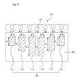
- the backlight unit 200 includes a light emitting device 100 and heat dissipating members 220 placed on a frame 210 .
- the heat dissipating members 220 may take the form of heat pipes and the frame 210 may be made of high strength metal, and for example, may be made of stainless steel having high corrosion resistance.
- the backlight unit in which light emitting elements, such as light emitting diodes, are arranged, tend to convert only about 20% of consumed energy into light and the remaining 80% is lost as heat based on optical characteristics of light emitting diodes, thereby disadvantageously increasing the interior temperature thereof.
- the temperature increase of the backlight unit may deteriorate the overall performance of the backlight unit.
- the backlight unit using light emitting diodes may suffer from deterioration in efficiency due to heat emission after extended use. Consequently, excessive increase in heat emission caused after extended use may reduce lifespan of the backlight unit.
- the backlight unit may need a heat dissipating structure.
- the heat dissipating members 220 in the form of heat pipes are provided.
- a thickness of the frame 210 may be in a range of 0.1 ⁇ 0.2 mm.
- the size of the frame 210 may be changed according to the size of a screen of a display device, such as a liquid crystal display usable with the backlight unit. In consideration of the screen of the display device, the frame 210 may have a rectangular shape.
- a supporting member may be mounted on the frame 210 and serve to support, e.g., the light emitting device 100 .
- the light emitting device 100 is a light emitting diode package including light emitting diodes.
- the light emitting diodes may emit light of various colors, such as red, green, blue, white and ultraviolet light, and may emit white light with high efficiency through use of fluorescent materials or combination of colors, thereby being advantageous for use in the backlight unit.
- the light emitting diode package 100 includes a light emitting diode 14 disposed on a package body 20 .
- the light emitting diode 14 is electrically connected to first and second electrodes 11 and 12 disposed on the package body 20 .
- the light emitting diode 14 may be fixed to the package body 20 through a bonding layer 16 .
- a heat dissipating pad may be disposed to absorb and dissipate heat emitted from the light emitting diode 14 .
- the package body 20 may be made of a silicone material, a synthetic resin material or a metallic material.
- a ramp is formed around the light emitting diode package 100 , thus serving to improve light extraction efficiency.
- the light emitting diode 14 may be electrically connected to the first and second electrodes 11 and 12 by either flip chips or die bonding, in addition to using bonding wires 15 as illustrated.
- the first electrode 11 and the second electrode 12 are electrically isolated of each other and serve to apply power to the light emitting diode 14 .
- the first electrode 11 and the second electrode 12 may function to reflect light emitted from the light emitting diode 14 so as to increase illumination efficiency and also, may function to dissipate heat generated from the light emitting diode 14 .
- a filler 18 may be disposed to surround the light emitting diode 14 , thus serving to protect the light emitting diode 14 .
- the filler 18 contains a fluorescent substance so as to change the wavelength of light emitted from the light emitting diode 14 .
- the light emitting diode package 100 further includes a lens 17 .
- the lens 17 may be placed on or surround the filler 18 , or may be formed on the package body 20 so as to cover the package body 20 .
- the lens 17 may serve to change a path of light emitted from the light emitting diode 14 .
- the lens 17 may be omitted as occasion demands.
- a light emitting device array which is comprised of a plurality of light emitting diode packages 100 fixed on a printed circuit board, may be fixed to a distal end of the frame 210 . This is equally applicable to the following embodiments.
- heat emitted from the light emitting diodes may be concentrated on the center of the backlight unit.
- center refers to an approximately middle location in a horizontal or vertical direction of the frame 210
- peripheral means an edge region of the frame 210 .
- the heat dissipating members 220 may be heat pipes.
- Such a heat pipe may be configured by filling a conductive pipe with a highly thermally conductive medium.
- the heat dissipating members 220 may be brought into contact with the printed circuit board on which the light emitting diode package 100 is fixed.
- the frame 210 may be disposed with a hole at a distal end of the heat dissipating member 220 , so as to enable dissipation of heat from the interior of the backlight unit.
- the distal end of the heat dissipating member 220 is at a location far away from the light emitting diode package 100 .
- the heat dissipating members 220 are arranged parallel to the direction of light emitted from the light emitting diode package 100 , and the area of the respective heat dissipating members 220 decreases from the center to the perimeter of the frame 210 .
- the area of the respective heat dissipating members 220 is determined based on a width thereof.
- the heat dissipating member 220 disposed at the center of the frame 210 may have the greatest width, and the width of the respective heat dissipating members 220 may gradually decrease toward the perimeter of the frame 210 .
- the width of the respective heat dissipating members 220 may decrease toward the perimeter in proportion to a distance from the center of the frame 210 .
- the five heat dissipating members L 11 , L 12 , L 13 , L 14 and L 15 have the same length or height h 1 , but have different widths W 11 , W 12 , W 13 , W 14 and W 15 respectively, such that the center heat dissipating member L 13 has the greatest width W 13 and the outermost heat dissipating members L 11 and L 15 have the smallest width W 11 and W 15 .
- the width W 11 of the outermost heat dissipating member may L 11 be in a range of 1 ⁇ 3 ⁇ 2 ⁇ 3 the width W 13 of the center heat dissipating member L 13 . If the width W 11 or W 15 is less than 1 ⁇ 3 the width W 13 , heat is not sufficiently dissipated at the perimeter. Also, if the width W 11 or W 15 is 2 ⁇ 3 or more the width W 13 , effects obtained by providing the center heat dissipating member with a thick thickness are inconsequential.
- FIG. 2A illustrates seven light emitting diode packages 100 and five heat dissipating members 220 , actually, a greater number of light emitting diode packages 110 and heat dissipating members 220 may be disposed.
- the heat dissipating members 220 are preferably made of a highly thermally conductive material.
- the heat dissipating members 220 may be made of aluminum (Al) or copper (Cu).
- the heat dissipating members 220 may be made of gold (Au) or silver (Ag) when taking no thought of costs.
- FIG. 2B is basically identical to the embodiment illustrated in FIG. 2A , but has a difference in that a pair of arrays of light emitting diode packages 100 is disposed at two opposing sides of the frame 210 .
- FIG. 3A is a view illustrating another embodiment of the backlight unit.
- the present embodiment is basically identical to the above-described embodiments, but has a difference in that a plurality of heat dissipating members 230 has different lengths.
- the heat dissipating member 230 disposed at the center of the frame 210 of the light emitting diode backlight unit has the greatest dimension.
- the dimension corresponds to the length of the heat dissipating member 230 .
- the heat dissipating member 230 located at the center of the frame 210 has the greatest length and the length of the respective heat dissipating members 230 decreases toward the perimeter.
- the length of the respective heat dissipating members 230 may gradually decrease toward the perimeter, i.e. toward the edge of the frame 210 in proportion to a distance from the center of the frame 210 .
- the five heat dissipating members L 21 , L 22 , L 23 , L 24 and L 25 have the same width W 21 , W 22 , W 23 , W 24 and W 25 , but have different heights (lengths) h 11 , h 12 , h 13 , h 14 and h 15 respectively, such that the center heat dissipating member L 23 has the greatest length h 13 and the outermost heat dissipating members L 21 and L 25 have the smallest length h 11 and h 15 .
- the length h 11 of the outermost heat dissipating member may be in a range of 1 ⁇ 3 ⁇ 2 ⁇ 3 the length h 13 of the center heat dissipating member. If the length h 11 is less than 1 ⁇ 3 the length h 13 , heat is not sufficiently dissipated at the perimeter. Also, if the length h 11 is 2 ⁇ 3 or more the width h 13 , effects obtained by providing the center heat dissipating member with a long length are inconsequential.
- the embodiment illustrated in FIG. 3B is basically identical to the embodiment illustrated in FIG. 3A , but has a difference in that the heat dissipating members 230 are bundled into two symmetrical groups.
- two groups, each consisting of the heat dissipating members L 21 , L 22 , L 23 , L 24 and L 25 are symmetrically arranged on the basis of an imaginary line that bisects the frame 210 into upper and lower parts.
- the heat dissipating members having the same area are horizontally symmetrically arranged on the basis of the center heat dissipating member.
- the length or width of the heat dissipating members may decrease toward the perimeter in proportion to a distance from the center of the frame 210 .
- heat conductivity may be calculated by the following Equation 1.
- Q represents heat flow, which is inversely proportional to the length L of a contact material and is proportional to a temperature variation ⁇ T of the material. Since increasing heat flow may necessitate to increase heat conductivity k of the heat dissipating member or the length of the contact material, the present embodiment proposes an increase in the area of the heat dissipating member so as to increase a contact length/area.
- the heat dissipating members having the same size/shape may be densely arranged at the center of the frame and be less densely arranged toward the perimeter.
- FIGS. 4A and 4B are views illustrating other embodiments of the backlight unit. These embodiments are basically identical to the above-described embodiments, but have a difference in that a plurality of heat dissipating members 240 ; L 31 , L 32 , L 33 , L 34 and L 35 has a trapezoidal shape. More specifically, in the case of the trapezoidal heat dissipating member 240 , one side thereof close to the light emitting diode package 100 has a greater width W 31 than the other end distant from the light emitting diode package 100 .
- the heat dissipating member 240 as illustrated in FIG. 4A may be provided in consideration of the fact that heat is concentrated at locations closer to the light emitting diode package 100 .
- FIG. 4B is a view illustrating another embodiment of the backlight unit.
- the present embodiment is basically identical to the above-described embodiment of FIG. 4A , but has a difference in that a plurality of trapezoidal heat dissipating members 250 ; L 41 , L 42 , L 43 , L 44 and L 45 has different sizes.
- the center heat dissipating member L 43 has the greatest area and the outermost heat dissipating members L 41 and L 45 have the smallest area.
- Each of the heat dissipating members has the greatest width W 41 , W 42 , W 43 , W 44 and W 45 at a portion thereof close to the light emitting diode package 100 and the width gradually decreases far away from the light emitting diode package 100 to W 41′ , W 42′ , W 43′ , W 44′ and W 45′ .
- the respective heat dissipating members have different lengths (heights) h 41 , h 42 , h 43 , h 44 and h 45 .
- the center heat dissipating member L 43 may have the greatest length h 43 and the outermost heat dissipating members L 41 and L 45 may have the smallest length h 41 and h 45 .
- the length of one of the heat dissipating members must be 1 ⁇ 3 or more the length of a shorter direction of the frame in order to achieve sufficient heat dissipation effects and is sufficient to be 2 ⁇ 3 or less the length of the shorter direction of the frame.
- the heat dissipating members have a thickness of 5 mm or less so as to enable production of an extremely slim backlight unit.
- an even number of heat dissipating members 260 is disposed. Specifically, although one heat dissipating member disposed at the very middle of the frame 210 has the greatest area in the above-described embodiments, in the present embodiment, the even number of heat dissipating members 260 is disposed such that the two center heat dissipating members 260 have the same area.
- FIG. 6 is a view illustrating an embodiment of a display device having the backlight unit according to the embodiment.
- the embodiment of the display device having the backlight unit according to the embodiment will be described with reference to FIG. 6 .
- the display device includes the backlight unit, a diffusion plate 300 , and a liquid crystal display member 310 and may further include a color filter 320 .
- an array of the light emitting diode packages 100 (hereinafter, simply referred to as a light emitting device) is disposed on at least one surface of the frame.
- a light emitting diode consists of nitride semiconductors including a p-type semiconductor layer, an active layer and an n-type semiconductor layer stacked one above another on a substrate.
- An n-type electrode and a p-type electrode of the light emitting diode are electrically connected to a mount lead and an inner lead respectively by use of wires.
- the light emitting diode is covered with a fluorescent layer that is made of a mixture of a transparent resin and a fluorescent material.
- the light emitting diode is received in a cup-shaped structure, thereby enabling unidirectional emission of light.
- the above-described backlight unit may include a reflective plate 270 and a light guide plate 280 .
- the light guide plate 280 serves to disperse light emitted from the light emitting diode package 100 so as to allow the light to be uniformly distributed throughout a screen of the liquid crystal display.
- the reflective plate 270 serves to reintroduce the light exiting downward from the light guide plate 280 into the light guide plate 280 without any loss.
- the frame of the backlight unit is disposed with heat dissipating members.
- the heat dissipating member disposed at the center of the frame is larger than the heat dissipating member disposed at the perimeter of the frame.
- the size of the heat dissipating member may be determined based on any one of the width, length and area of the heat dissipating member.
- the heat dissipating member may have a trapezoidal shape gradually decreasing in width from a side thereof close to the light emitting device to an opposite side thereof distant from the light emitting device.
- a coupling configuration of the frame and the heat dissipating members also follows the above description.
- the diffusion plate 300 which serves as a lens, is placed on the light guide plate 280 so as to diffuse the light directed from the light guide plate 280 by a predetermined angle.
- the liquid crystal display member 310 is placed on a front surface of the diffusion plate 300 .
- other kinds of display members requiring a light emitting device other than the liquid crystal display member 310 may be disposed.
- the liquid crystal display member 310 is configured such that liquid crystals are filled between glass substrates and a pair of polarizing plates is placed respectively on the glass substrates.
- the liquid crystals are regularly arranged organic molecules having properties between solid and liquid and thus, having fluidity.
- the molecular arrangement of liquid crystals is changed by an exterior electric field, enabling display of an image.
- the liquid crystal display member used in the display device is of an active matrix type and includes transistors serving as switches to control application of voltage to each pixel.
- liquid crystal display member A detailed configuration of the liquid crystal display member is well known and thus, a description thereof will be omitted herein.
- the color filter 320 may be placed on a front surface of the liquid crystal display member 310 .
- the color filter 320 functions to display an image in such a manner that each pixel acts to transmit only red, blue or green light projected from the liquid crystal display member 310 .
- an edge type light emitting diode backlight unit is disposed at only some of four sides of the frame with light emitting diodes, distribution of heat emitted from the light emitting diodes may be concentrated at the center of the backlight unit.
- the center of the backlight unit requires a more efficient heat dissipating configuration than the edge of the backlight unit.
- An insufficient heat dissipating configuration may cause overheating of the center of the backlight unit and distortion of the frame and consequently, malfunction of the backlight unit or the display device.
- heat dissipating members in the form of heat pipes are arranged on a frame of the backlight unit such that the width of the respective heat dissipating members gradually decreases from the center to the perimeter of the backlight unit, thereby achieving efficient dissipation of heat concentrated at the center of the backlight unit.
- At least one of the width, length and area of these heat dissipating members may decrease or increase from the center to the perimeter of the backlight unit so as to effectively dissipate heat concentrated at the center of the backlight unit, whereby distortion of the frame and consequently, malfunction of the backlight unit and/or the display device can be prevented.
Abstract
Description
Claims (20)
Applications Claiming Priority (2)
| Application Number | Priority Date | Filing Date | Title |
|---|---|---|---|
| KR1020100041398A KR101025543B1 (en) | 2010-05-03 | 2010-05-03 | Backlight unit and display unit including the same |
| KR10-2010-0041398 | 2010-05-03 |
Publications (2)
| Publication Number | Publication Date |
|---|---|
| US20110267837A1 US20110267837A1 (en) | 2011-11-03 |
| US8602624B2 true US8602624B2 (en) | 2013-12-10 |
Family
ID=44049430
Family Applications (1)
| Application Number | Title | Priority Date | Filing Date |
|---|---|---|---|
| US13/070,133 Active - Reinstated 2032-01-18 US8602624B2 (en) | 2010-05-03 | 2011-03-23 | Backlight unit and display device having the same |
Country Status (5)
| Country | Link |
|---|---|
| US (1) | US8602624B2 (en) |
| EP (1) | EP2385418B1 (en) |
| JP (1) | JP5755928B2 (en) |
| KR (1) | KR101025543B1 (en) |
| CN (1) | CN102235623B (en) |
Families Citing this family (4)
| Publication number | Priority date | Publication date | Assignee | Title |
|---|---|---|---|---|
| WO2013031319A1 (en) * | 2011-08-29 | 2013-03-07 | パナソニック液晶ディスプレイ株式会社 | Liquid-crystal display device and television receiver |
| US9702527B2 (en) * | 2012-03-22 | 2017-07-11 | Lite-On Electronics (Guangzhou) Limited | Light emitting device |
| JP6079409B2 (en) * | 2013-04-23 | 2017-02-15 | 三菱電機株式会社 | Liquid crystal display |
| CN114967239B (en) * | 2022-07-29 | 2022-11-25 | 惠科股份有限公司 | Back plate of backlight module, backlight module and display device |
Citations (11)
| Publication number | Priority date | Publication date | Assignee | Title |
|---|---|---|---|---|
| KR20030052980A (en) | 2001-12-20 | 2003-06-27 | 후지쯔 디스플레이 테크놀로지스 코포레이션 | Backlight device |
| JP2004004581A (en) | 2002-04-04 | 2004-01-08 | Seiko Epson Corp | Heat sink member, lighting device, electro-optical device, and electronic device |
| KR20060012917A (en) | 2004-08-05 | 2006-02-09 | 삼성전자주식회사 | Backlight assembly |
| US20060072344A1 (en) * | 2004-10-05 | 2006-04-06 | Kim Won-Nyun | Backlight unit |
| KR20060099365A (en) | 2005-03-12 | 2006-09-19 | 삼성전자주식회사 | Edge light type back light unit having heat sink system |
| US20060262571A1 (en) * | 2005-05-18 | 2006-11-23 | Hon Hai Precision Industry Co., Ltd. | Backlight module and method for making the same |
| US20070211184A1 (en) | 2006-03-10 | 2007-09-13 | Luminus Devices, Inc. | Liquid crystal display systems including LEDs |
| US20080304288A1 (en) | 2007-06-08 | 2008-12-11 | Fujifilm Corporation | Planar lighting device |
| US7488104B2 (en) * | 2004-05-21 | 2009-02-10 | Sharp Kabushiki Kaisha | Backlight unit and liquid crystal display device having the same |
| WO2009099547A2 (en) | 2008-01-30 | 2009-08-13 | Digital Optics International, Llc | Thin illumination system |
| KR20090120556A (en) | 2008-05-20 | 2009-11-25 | 삼성전자주식회사 | Back light assembly and display device having the same |
Family Cites Families (2)
| Publication number | Priority date | Publication date | Assignee | Title |
|---|---|---|---|---|
| US8031292B2 (en) * | 2006-11-21 | 2011-10-04 | Samsung Electronics Co., Ltd. | Liquid crystal display comprising first and second point light source assemblies wherein a first support substrate is larger than the second support substrate, and a first groove of a lower container is deeper than a second groove |
| JP2010097924A (en) * | 2008-09-18 | 2010-04-30 | Hitachi Ltd | Liquid crystal display unit |
-
2010
- 2010-05-03 KR KR1020100041398A patent/KR101025543B1/en active IP Right Grant
-
2011
- 2011-03-23 US US13/070,133 patent/US8602624B2/en active Active - Reinstated
- 2011-03-28 EP EP11160030.0A patent/EP2385418B1/en active Active
- 2011-04-06 JP JP2011084754A patent/JP5755928B2/en active Active
- 2011-04-15 CN CN201110096957.7A patent/CN102235623B/en not_active Expired - Fee Related
Patent Citations (12)
| Publication number | Priority date | Publication date | Assignee | Title |
|---|---|---|---|---|
| KR20030052980A (en) | 2001-12-20 | 2003-06-27 | 후지쯔 디스플레이 테크놀로지스 코포레이션 | Backlight device |
| JP2004004581A (en) | 2002-04-04 | 2004-01-08 | Seiko Epson Corp | Heat sink member, lighting device, electro-optical device, and electronic device |
| US7488104B2 (en) * | 2004-05-21 | 2009-02-10 | Sharp Kabushiki Kaisha | Backlight unit and liquid crystal display device having the same |
| KR20060012917A (en) | 2004-08-05 | 2006-02-09 | 삼성전자주식회사 | Backlight assembly |
| US20060072344A1 (en) * | 2004-10-05 | 2006-04-06 | Kim Won-Nyun | Backlight unit |
| KR20060099365A (en) | 2005-03-12 | 2006-09-19 | 삼성전자주식회사 | Edge light type back light unit having heat sink system |
| US20060262571A1 (en) * | 2005-05-18 | 2006-11-23 | Hon Hai Precision Industry Co., Ltd. | Backlight module and method for making the same |
| US20070211184A1 (en) | 2006-03-10 | 2007-09-13 | Luminus Devices, Inc. | Liquid crystal display systems including LEDs |
| US20080304288A1 (en) | 2007-06-08 | 2008-12-11 | Fujifilm Corporation | Planar lighting device |
| US7766534B2 (en) * | 2007-06-08 | 2010-08-03 | Fujifilm Corporation | Planar lighting device |
| WO2009099547A2 (en) | 2008-01-30 | 2009-08-13 | Digital Optics International, Llc | Thin illumination system |
| KR20090120556A (en) | 2008-05-20 | 2009-11-25 | 삼성전자주식회사 | Back light assembly and display device having the same |
Also Published As
| Publication number | Publication date |
|---|---|
| US20110267837A1 (en) | 2011-11-03 |
| JP5755928B2 (en) | 2015-07-29 |
| EP2385418A3 (en) | 2012-04-04 |
| KR101025543B1 (en) | 2011-04-04 |
| CN102235623A (en) | 2011-11-09 |
| JP2011238598A (en) | 2011-11-24 |
| EP2385418B1 (en) | 2017-09-13 |
| CN102235623B (en) | 2015-08-05 |
| EP2385418A2 (en) | 2011-11-09 |
Similar Documents
| Publication | Publication Date | Title |
|---|---|---|
| US10096647B2 (en) | Display apparatus having a plurality of reflective electrodes | |
| US9705054B2 (en) | Light emitting device module | |
| US9022632B2 (en) | LED package and a backlight unit unit comprising said LED package | |
| US10054733B2 (en) | Light emitting device package and display device including the same | |
| US8842255B2 (en) | Light source module and lighting apparatus having the same | |
| KR102067420B1 (en) | Light emitting diode assembly and liquid crystal display device having the same | |
| US8625053B2 (en) | Light emitting diode and backlight unit and liquid crystal display device with the same | |
| US20110292679A1 (en) | Backlight unit and display device having the same | |
| US8602624B2 (en) | Backlight unit and display device having the same | |
| KR101774277B1 (en) | Liquid crystal display device | |
| KR101850434B1 (en) | Light emitting device module and lighting system including the same | |
| KR102068766B1 (en) | LED assembly and liquid crystal display device using the same | |
| KR20120100357A (en) | Backlight unit | |
| US20120250288A1 (en) | Light source heat-dissipation structure of backlight module | |
| KR101323401B1 (en) | Light divice, method of fabricating the same, backlight unit and liquid crystal display divice having the same | |
| KR101729776B1 (en) | Backlgiht unit and liquid crystal display device the same | |
| US20230046652A1 (en) | Light emitting diode package and backlight unit including the same | |
| KR100696063B1 (en) | Array emitting device | |
| KR101978941B1 (en) | Light Emitting Device Package | |
| KR102462304B1 (en) | Light emitting package, backlight unit and lighting device | |
| KR20150077166A (en) | Light emitting diode assembly and method of fabricating the same and liquid crystal display device having the same | |
| KR20130113027A (en) | Backlight unit | |
| KR101942253B1 (en) | Phosphor and light emitting diode having the same | |
| KR20120133811A (en) | Light emitting diode package | |
| KR20140075392A (en) | Light emitting device package and backlight unit thereof |
Legal Events
| Date | Code | Title | Description |
|---|---|---|---|
| AS | Assignment |
Owner name: LG INNOTEK CO., LTD., KOREA, REPUBLIC OF Free format text: ASSIGNMENT OF ASSIGNORS INTEREST;ASSIGNORS:LEE, SANG HOON;LEE, HAE HYUNG;REEL/FRAME:026017/0758 Effective date: 20110318 |
|
| FEPP | Fee payment procedure |
Free format text: PAYOR NUMBER ASSIGNED (ORIGINAL EVENT CODE: ASPN); ENTITY STATUS OF PATENT OWNER: LARGE ENTITY |
|
| REMI | Maintenance fee reminder mailed | ||
| LAPS | Lapse for failure to pay maintenance fees |
Free format text: PATENT EXPIRED FOR FAILURE TO PAY MAINTENANCE FEES (ORIGINAL EVENT CODE: EXP.) |
|
| FP | Lapsed due to failure to pay maintenance fee |
Effective date: 20171210 |
|
| FEPP | Fee payment procedure |
Free format text: SURCHARGE, PETITION TO ACCEPT PYMT AFTER EXP, UNINTENTIONAL (ORIGINAL EVENT CODE: M1558); ENTITY STATUS OF PATENT OWNER: LARGE ENTITY Free format text: PETITION RELATED TO MAINTENANCE FEES GRANTED (ORIGINAL EVENT CODE: PMFG); ENTITY STATUS OF PATENT OWNER: LARGE ENTITY Free format text: PETITION RELATED TO MAINTENANCE FEES FILED (ORIGINAL EVENT CODE: PMFP); ENTITY STATUS OF PATENT OWNER: LARGE ENTITY |
|
| MAFP | Maintenance fee payment |
Free format text: PAYMENT OF MAINTENANCE FEE, 4TH YEAR, LARGE ENTITY (ORIGINAL EVENT CODE: M1551); ENTITY STATUS OF PATENT OWNER: LARGE ENTITY Year of fee payment: 4 |
|
| PRDP | Patent reinstated due to the acceptance of a late maintenance fee |
Effective date: 20180924 |
|
| STCF | Information on status: patent grant |
Free format text: PATENTED CASE |
|
| MAFP | Maintenance fee payment |
Free format text: PAYMENT OF MAINTENANCE FEE, 8TH YEAR, LARGE ENTITY (ORIGINAL EVENT CODE: M1552); ENTITY STATUS OF PATENT OWNER: LARGE ENTITY Year of fee payment: 8 |
|
| AS | Assignment |
Owner name: SUZHOU LEKIN SEMICONDUCTOR CO., LTD., CHINA Free format text: ASSIGNMENT OF ASSIGNORS INTEREST;ASSIGNOR:LG INNOTEK CO., LTD.;REEL/FRAME:056366/0335 Effective date: 20210520 |