US8525328B2 - Power device package structure - Google Patents
Power device package structure Download PDFInfo
- Publication number
- US8525328B2 US8525328B2 US13/182,469 US201113182469A US8525328B2 US 8525328 B2 US8525328 B2 US 8525328B2 US 201113182469 A US201113182469 A US 201113182469A US 8525328 B2 US8525328 B2 US 8525328B2
- Authority
- US
- United States
- Prior art keywords
- metal
- power device
- base plate
- terminal
- dielectric material
- Prior art date
- Legal status (The legal status is an assumption and is not a legal conclusion. Google has not performed a legal analysis and makes no representation as to the accuracy of the status listed.)
- Active, expires
Links
Images


Classifications
-
- H—ELECTRICITY
- H01—ELECTRIC ELEMENTS
- H01L—SEMICONDUCTOR DEVICES NOT COVERED BY CLASS H10
- H01L25/00—Assemblies consisting of a plurality of individual semiconductor or other solid state devices ; Multistep manufacturing processes thereof
- H01L25/16—Assemblies consisting of a plurality of individual semiconductor or other solid state devices ; Multistep manufacturing processes thereof the devices being of types provided for in two or more different main groups of groups H01L27/00 - H01L33/00, or in a single subclass of H10K, H10N, e.g. forming hybrid circuits
- H01L25/165—Containers
-
- H—ELECTRICITY
- H01—ELECTRIC ELEMENTS
- H01L—SEMICONDUCTOR DEVICES NOT COVERED BY CLASS H10
- H01L2224/00—Indexing scheme for arrangements for connecting or disconnecting semiconductor or solid-state bodies and methods related thereto as covered by H01L24/00
- H01L2224/01—Means for bonding being attached to, or being formed on, the surface to be connected, e.g. chip-to-package, die-attach, "first-level" interconnects; Manufacturing methods related thereto
- H01L2224/42—Wire connectors; Manufacturing methods related thereto
- H01L2224/47—Structure, shape, material or disposition of the wire connectors after the connecting process
- H01L2224/48—Structure, shape, material or disposition of the wire connectors after the connecting process of an individual wire connector
- H01L2224/4805—Shape
- H01L2224/4809—Loop shape
- H01L2224/48091—Arched
-
- H—ELECTRICITY
- H01—ELECTRIC ELEMENTS
- H01L—SEMICONDUCTOR DEVICES NOT COVERED BY CLASS H10
- H01L2224/00—Indexing scheme for arrangements for connecting or disconnecting semiconductor or solid-state bodies and methods related thereto as covered by H01L24/00
- H01L2224/01—Means for bonding being attached to, or being formed on, the surface to be connected, e.g. chip-to-package, die-attach, "first-level" interconnects; Manufacturing methods related thereto
- H01L2224/42—Wire connectors; Manufacturing methods related thereto
- H01L2224/47—Structure, shape, material or disposition of the wire connectors after the connecting process
- H01L2224/48—Structure, shape, material or disposition of the wire connectors after the connecting process of an individual wire connector
- H01L2224/481—Disposition
- H01L2224/48151—Connecting between a semiconductor or solid-state body and an item not being a semiconductor or solid-state body, e.g. chip-to-substrate, chip-to-passive
- H01L2224/48221—Connecting between a semiconductor or solid-state body and an item not being a semiconductor or solid-state body, e.g. chip-to-substrate, chip-to-passive the body and the item being stacked
- H01L2224/48245—Connecting between a semiconductor or solid-state body and an item not being a semiconductor or solid-state body, e.g. chip-to-substrate, chip-to-passive the body and the item being stacked the item being metallic
- H01L2224/48247—Connecting between a semiconductor or solid-state body and an item not being a semiconductor or solid-state body, e.g. chip-to-substrate, chip-to-passive the body and the item being stacked the item being metallic connecting the wire to a bond pad of the item
-
- H—ELECTRICITY
- H01—ELECTRIC ELEMENTS
- H01L—SEMICONDUCTOR DEVICES NOT COVERED BY CLASS H10
- H01L23/00—Details of semiconductor or other solid state devices
- H01L23/28—Encapsulations, e.g. encapsulating layers, coatings, e.g. for protection
- H01L23/31—Encapsulations, e.g. encapsulating layers, coatings, e.g. for protection characterised by the arrangement or shape
- H01L23/3107—Encapsulations, e.g. encapsulating layers, coatings, e.g. for protection characterised by the arrangement or shape the device being completely enclosed
-
- H—ELECTRICITY
- H01—ELECTRIC ELEMENTS
- H01L—SEMICONDUCTOR DEVICES NOT COVERED BY CLASS H10
- H01L2924/00—Indexing scheme for arrangements or methods for connecting or disconnecting semiconductor or solid-state bodies as covered by H01L24/00
- H01L2924/10—Details of semiconductor or other solid state devices to be connected
- H01L2924/11—Device type
- H01L2924/13—Discrete devices, e.g. 3 terminal devices
- H01L2924/1304—Transistor
- H01L2924/1305—Bipolar Junction Transistor [BJT]
- H01L2924/13055—Insulated gate bipolar transistor [IGBT]
-
- H—ELECTRICITY
- H01—ELECTRIC ELEMENTS
- H01L—SEMICONDUCTOR DEVICES NOT COVERED BY CLASS H10
- H01L2924/00—Indexing scheme for arrangements or methods for connecting or disconnecting semiconductor or solid-state bodies as covered by H01L24/00
- H01L2924/10—Details of semiconductor or other solid state devices to be connected
- H01L2924/11—Device type
- H01L2924/13—Discrete devices, e.g. 3 terminal devices
- H01L2924/1304—Transistor
- H01L2924/1306—Field-effect transistor [FET]
- H01L2924/13091—Metal-Oxide-Semiconductor Field-Effect Transistor [MOSFET]
-
- H—ELECTRICITY
- H01—ELECTRIC ELEMENTS
- H01L—SEMICONDUCTOR DEVICES NOT COVERED BY CLASS H10
- H01L2924/00—Indexing scheme for arrangements or methods for connecting or disconnecting semiconductor or solid-state bodies as covered by H01L24/00
- H01L2924/30—Technical effects
- H01L2924/301—Electrical effects
- H01L2924/30107—Inductance
Definitions
- the disclosure generally relates to a power device package structure. More particularly, the disclosure relates to a package structure incorporating the capacitor and/or resistor with the power device.
- the package structure includes a metal base plate 28 B, a power device 20 and a package resin 23 .
- the metal base plate 28 B has a locking area 21 and a central planar area 22 .
- the locking area 21 having a hole 26 is exposed out of the package resin 23 , while the package structure can be locked, via the hole 26 , to the printed circuit board, a base or other metal heat sinks for heat dissipation.
- a central metal lead D is extended from the central planar area 22 of the metal base plate 28 B, while a first metal lead G and a second metal lead S are respectively arranged coplanarly on both sides of the central metal lead D.
- the power device 20 is disposed on the central planar area 22 of the metal base plate 28 B and has a gate terminal GT, a drain terminal DT and a source terminal ST electrically connected to the metal leads G, D and S respectively, through wires 24 .
- the three terminals GT, DT and ST are coplanarly arranged.
- the three terminals GT, DT and ST are vertically arranged.
- the conventional package structure does not include capacitors, and the capacitor is electrically connected with the package structure but arranged outside of the package structure.
- Such design causes longer metal wires or conductive path between the power device and the capacitor, leading to higher parasite inductance effects and more power consumption.
- the disclosure of an embodiment provide a power device package structure.
- the power device package structure include a metal base plate, a dielectric material layer disposed on the metal base plate, an upper metal layer disposed on the dielectric material layer and at least a power device disposed on the metal base plate.
- the upper metal layer, the dielectric material, layer and the metal base plate form a capacitor.
- the disclosure of another embodiment provide a power device package structure.
- the power device package structure include a metal base plate, a dielectric material layer disposed on the metal base plate, an upper metal layer disposed on the dielectric material layer, and at least one power device disposed on the upper metal layer, wherein the upper metal layer, the dielectric material layer and the metal base plate form a capacitor.
- FIG. 1 illustrates a conventional power device package structure.
- FIG. 2 illustrates a conventional power device package structure.
- FIG. 3 illustrates an exemplary top view of a power device package structure according to one embodiment of the disclosure.
- FIG. 4 illustrates an exemplary top view of a power device package structure according to another embodiment of the disclosure.
- FIG. 5 shows the equivalent circuit of the package structure of FIGS. 3 & 4 .
- FIG. 6 is shown in a cross-sectional view of FIG. 3 along line A-A′.
- FIG. 7 is shown in a cross-sectional view of FIG. 4 along line A-A′.
- FIG. 8 is shown in a cross-sectional view of FIG. 3 along line B-B′.
- FIG. 9 is shown in a cross-sectional view of FIG. 4 along line B-B′.
- FIG. 10 illustrates an exemplary top view of a power device package structure according to another embodiment of the disclosure.
- FIG. 11 illustrates an exemplary top view of a power device package structure according to another embodiment of the disclosure.
- FIG. 12 shows the equivalent circuit of the package structure of FIGS. 10 & 11 .
- FIG. 13 is shown in a cross-sectional view of FIG. 11 along line C-C′.
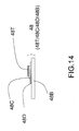
- FIG. 14 illustrates an exemplary cross-sectional view of a power device package structure according to another embodiment of the disclosure.
- FIG. 15 shows the equivalent circuit of the package structure of the disclosure.
- the disclosure provides a power device package structure by incorporating the capacitor into the package structure, which reduces the package structure and decreases the production costs. Because the capacitor is located within the package structure, the wiring length between the components can be shortened and the equivalent serial inductance (ESL) and parasite inductance effect can be lessened, along with less power loss.
- ESL equivalent serial inductance
- the disclosure provides a package structure incorporating the capacitor and/or resistor with the power device.
- the metal base plate functions as the lower electrode of the capacitor
- the capacitor can be formed by arranging a dielectric material layer on the metal base plate and an upper metal layer on the dielectric layer.
- the disclosure provides a power device package structure incorporating the capacitor within the package structure.
- the capacitor can be formed by arranging a dielectric material layer on the metal base plate and an upper metal layer on the dielectric material layer.
- the power device package structure of the disclosure may optionally incorporate one or more resistors on the dielectric material layer of the power device.
- the wiring length or conductive path between the passive components, such as capacitors or resistors, and the power device can be effectively shortened. Therefore, the parasite inductance effect of the power source transmission loop for the above mentioned components can be lessened. If the RC snubber circuit is directly added to the package structure to flatten the high frequency spike, the IV overlapping area of the IV curve will be decreased. The switch energy (power) loss of the power device is reduced when the overlapping area is reduced.
- the power device package structure of the disclosure can lessen the parasite inductance effect and lower the energy loss, which improves the power source transmission efficiency and achieves energy saving.
- the power device of the disclosure can be any power device in the electronic or semiconductor industry, and the power device of the disclosure includes, but not limited to, the insulated gate bipolar transistor (IGBT) or metal oxide semiconductor field effect transistor (MOSFET).
- IGBT insulated gate bipolar transistor
- MOSFET metal oxide semiconductor field effect transistor
- FIG. 3 illustrates an exemplary top view of a power device package structure according to one embodiment of the disclosure.
- FIG. 6 is shown in a cross-sectional view of FIG. 3 along line A-A′
- FIG. 8 is shown in a cross-sectional view of FIG. 3 along line B-B′.
- FIG. 4 illustrates an exemplary top view of a power device package structure according to another embodiment of the disclosure.
- FIG. 7 is shown in a cross-sectional view of FIG. 4 along line A-A′
- FIG. 9 is shown in a cross-sectional view of FIG. 4 along line B-B′.
- the package structure 2 includes at least a power device 20 , an package resin 23 , a metal base plate 28 B, a dielectric material layer 28 D and an upper metal layer 28 T.
- the power device 20 is disposed on the metal base plate 28 B and is electrically connected to the metal base plate 28 B through at least a wire 24 .
- the material of the metal base plate 28 B can be aluminum or aluminum alloys, for example.
- the metal base plate 28 B is an integral sheet and has a locking area 21 , a central planar area 22 and a central metal lead D.
- the central planar area 22 is located between the locking area 21 and the central metal lead D.
- the locking area 21 having a hole 26 is exposed outside of the package resin 23 .
- the package structure 2 can be locked, via the hole 26 , to the printed circuit board, a base or other metal heat sinks for heat dissipation.
- the central metal lead D is protruded from the central planar area 22 of the metal base plate 28 B, while a first metal lead G and a second metal lead S are respectively arranged coplanarly on both sides of the central metal lead D.
- the first metal lead G, second metal lead S and central metal lead D are individual and separate from one another.
- the package resin 23 covers and protects the components on the metal base plate 28 B, and the covering area of the package resin 23 is shown in dotted line in FIG. 3 .
- the material of the package resin 23 can be epoxy resin, for example.
- the package resin 23 covers and protects the power device 20 , the upper metal layer 28 T, the resistor 25 , the dielectric material layer 28 D and the metal wire 24 .
- the first metal lead G, second metal lead S and central metal lead D respectively function as a gate metal lead, a source metal lead and a drain metal lead.
- the power device 20 is disposed on the central planar area 22 of the metal base plate 28 B and has a gate terminal GT, a drain terminal DT and a source terminal ST electrically connected to the metal leads G, D and S respectively, through wires 24 .
- the upper surfaces of the first and second metal leads G, S are coplanar with the upper surface of the central metal lead D, while the first and second metal leads G, S are arranged on both sides of the central metal lead D.
- the three terminals GT, DT and ST are coplanarly arranged.
- the three terminals GT, DT and ST are coplanarly arranged, or so called vertically arranged.
- the terminals GT, ST are arranged on the top of the power device 20 , while the terminal DT is arranged in the bottom of the power device 20 .
- The, number, location or shape of the metal lead(s) shown in this embodiment is not limited by the figures and can be adjusted according to the design of the products and well understood by the artisans.
- the dielectric material layer 28 D is disposed on the central planar area 22 of the metal base plate 28 B, while the upper metal layer 28 T is disposed on the dielectric material layer 28 D.
- the resistor 25 can be disposed on the dielectric material layer 28 D optionally.
- the upper metal layer 28 T is electrically connected with the resistor 25 through the wire 24 , while the resistor 25 is electrically connected to the source terminal ST of the power device 20 .
- the material of the dielectric material layer 28 D can be Al 2 O 3 , metalized polypropylene/polypropylene, metalized polyethylene/polyethylene or polyimide, or other applicable materials, for example.
- the upper metal layer 28 T, the dielectric material layer 28 D and the metal base plate 28 B together form a capacitor 28 .
- the metal base plate 28 B is used as the lower electrode (i.e. the lower metal layer) of the capacitor 28 , which reduces the production costs for separately disposing an extra metal layer as the lower metal layer of the capacitor.
- the power device 20 and the dielectric material layer 28 D are disposed on the planar area 22 of the base plate 28 B, while the upper metal layer 28 T is located on the dielectric material layer 28 D.
- the dielectric material layer 28 D is located beside but separate from the power device 20
- the resistor 25 is located beside but separate from the upper metal layer 28 T.
- the package resin 23 covers and protects the power device 20 , the capacitor 28 (including the upper metal layer 28 T, the dielectric material layer 28 D and the metal base plate 28 B) and the resistor 25 .
- FIG. 5 shows the equivalent circuit of the package structure of FIG. 3 or FIG. 4 .
- One terminal of the capacitor 28 is electrically connected to the drain terminal DT of the power device 20
- the other terminal of the capacitor 28 is electrically connected to one terminal of the resistor 25
- the other terminal of the resistor 25 is electrically connected to the source terminal ST of the power device 20 .
- FIG. 6 is shown in a cross-sectional view of FIG. 3 along line A-A′.
- FIG. 7 is shown in a cross-sectional view of FIG. 4 along line A-A′.
- the upper metal layer 28 T, the dielectric material layer 28 D and the metal base plate 28 B together form a capacitor 28 .
- the metal base plate 28 B is used as the lower electrode (i.e. the lower metal layer) of the capacitor 28 and the base plate of the package structure 2 .
- the upper metal layer 28 T is electrically connected with the resistor 25 through the wire 24
- the metal base plate 28 B is electrically connected to the drain terminal DT of the power device 20 through the wire 24 .
- FIG. 8 is shown in a cross-sectional view of FIG. 3 along line B-B′.
- FIG. 9 is shown in a cross-sectional view of FIG. 4 along line B-B′.
- the resistor 25 is located on the dielectric material layer 28 D.
- the resistor 25 is electrically connected with the upper metal layer 28 T and the source terminal ST of the power device 20 through the wires 24 .
- the package resin 23 encapsulates the components on the metal base plate 28 B.
- FIG. 10 illustrates an exemplary top view of a power device package structure according to another embodiment of the disclosure.
- the power device 30 is disposed on the upper metal layer 38 T.
- the resistor 35 can be arranged beside the upper metal layer 38 T, and the resistor 35 and the upper metal layer 38 T are both located on the dielectric material layer 38 D.
- the capacitor 38 consisting of the upper metal layer 38 T, the dielectric material layer 38 D and the metal base plate 38 B is located below the power device 30 .
- the metal base plate 38 B functions as the lower electrode (i.e. the lower metal layer) of the capacitor 38 and as the base of the package structure 3 .
- the dielectric material layer 38 D is disposed on the central planar area of the metal base plate 38 B.
- the package structure shown in FIG. 11 is similar to the package structure of FIG. 10 , except the three terminals GT, DT and ST are vertically arranged. The three terminals GT, DT and ST are coplanarly arranged for the package structure of FIG. 10 .
- FIG. 12 shows the equivalent circuit of the package structure of FIG. 10 or FIG. 11 .
- the capacitor 38 in FIG. 12 consists of the upper metal layer 38 T, the dielectric material layer 38 D and the metal base plate 38 B and is located below the power device 30 .
- the package resin 33 covers and protects the power device 30 , the capacitor 38 (including the upper metal layer 38 T, the dielectric material layer 38 D and the metal base plate 38 B) and the resistor 35 .
- One terminal of the capacitor 38 is electrically connected to the drain terminal DT of the power device 30
- the other terminal of the capacitor 38 is electrically connected to one terminal of the resistor 35
- the other terminal of the resistor 35 is electrically connected to the source terminal ST of the power device 30 .
- FIG. 13 is shown in a cross-sectional view of FIG. 11 along line C-C′.
- the dielectric material layer 38 D is disposed on the metal base plate 38 B
- the upper metal layer 38 T is disposed on the dielectric material layer 38 D
- the resistor 35 is disposed on the dielectric material layer 38 D.
- the upper metal layer 38 T, the dielectric material layer 38 D and the metal base plate 38 B together form a capacitor 38 .
- the metal base plate 38 B is used as the lower electrode (i.e. the lower metal layer) of the capacitor 38 and the base plate of the package structure 3 .
- the upper metal layer 38 T is electrically connected with one terminal of the resistor 35 through the wire 34
- the power device 30 is electrically connected to the other terminal of the resistor 35 through the wire 34 .
- FIG. 14 illustrates an exemplary cross-sectional view of a power device package structure according to another embodiment of the disclosure.
- the capacitor 48 further includes a conductive polymer layer 48 C between the upper metal layer 48 T and the dielectric material layer 48 D to enhance the capacitance efficiency.
- the material of the conductive polymer layer 48 C can be poly(3,4-ethylenedioxythiophene) (PEDOT), for example.
- FIG. 15 shows the equivalent circuit of the modification of the package structure based on the circuit shown in FIG. 5 and FIG. 12 .
- the connection relationship of the resistor R and the capacitor C can be switched by adjusting the relative positions or locations of the components in structural design. Such modification or adjustments is well understood and is encompassed within the protection scope of the disclosure.
Abstract
The disclosure relates to a power device package structure. By employing the metal substrate of the power device package structure serve as a bottom electrode of a capacitor, the capacitor is integrated into the power device package structure. A dielectric material layer and a upper metal layer sequentially disposed on the metal substrate.
Description
This application claims the priority benefit of Taiwan application serial no. 99146763, filed Dec. 30, 2010. The entirety of the above-mentioned patent application is hereby incorporated by reference herein and made a part of this specification.
1. Technical Field
The disclosure generally relates to a power device package structure. More particularly, the disclosure relates to a package structure incorporating the capacitor and/or resistor with the power device.
2. Technical Art
For the conventional package structure shown in FIG. 1 , the package structure includes a metal base plate 28B, a power device 20 and a package resin 23. The metal base plate 28B has a locking area 21 and a central planar area 22. The locking area 21 having a hole 26 is exposed out of the package resin 23, while the package structure can be locked, via the hole 26, to the printed circuit board, a base or other metal heat sinks for heat dissipation. A central metal lead D is extended from the central planar area 22 of the metal base plate 28B, while a first metal lead G and a second metal lead S are respectively arranged coplanarly on both sides of the central metal lead D. The power device 20 is disposed on the central planar area 22 of the metal base plate 28B and has a gate terminal GT, a drain terminal DT and a source terminal ST electrically connected to the metal leads G, D and S respectively, through wires 24. For the conventional package structure shown in FIG. 1 , the three terminals GT, DT and ST are coplanarly arranged. However, for the conventional package structure shown in FIG. 2 , the three terminals GT, DT and ST are vertically arranged.
However, the conventional package structure does not include capacitors, and the capacitor is electrically connected with the package structure but arranged outside of the package structure. Such design causes longer metal wires or conductive path between the power device and the capacitor, leading to higher parasite inductance effects and more power consumption.
The disclosure of an embodiment provide a power device package structure. The power device package structure include a metal base plate, a dielectric material layer disposed on the metal base plate, an upper metal layer disposed on the dielectric material layer and at least a power device disposed on the metal base plate. The upper metal layer, the dielectric material, layer and the metal base plate form a capacitor.
The disclosure of another embodiment provide a power device package structure. The power device package structure include a metal base plate, a dielectric material layer disposed on the metal base plate, an upper metal layer disposed on the dielectric material layer, and at least one power device disposed on the upper metal layer, wherein the upper metal layer, the dielectric material layer and the metal base plate form a capacitor.
The accompanying drawings are included to provide a further understanding of the invention, and are incorporated in and constitute a part of this specification. The drawings illustrate embodiments of the invention and, together with the description, serve to explain the principles of the invention.
Common reference numerals are used throughout the drawings and the detailed description to indicate the same elements. The disclosure will be more apparent from the following detailed description taken in conjunction with the accompanying drawings.
In the following detailed description, for purposes of explanation, numerous specific details are set forth in order to provide a thorough understanding of the disclosed embodiments. It will be apparent, however, that one or more embodiments may be practiced without these specific details. In other instances, well-known structures and devices are schematically shown in order to simplify the drawing.
The disclosure provides a power device package structure by incorporating the capacitor into the package structure, which reduces the package structure and decreases the production costs. Because the capacitor is located within the package structure, the wiring length between the components can be shortened and the equivalent serial inductance (ESL) and parasite inductance effect can be lessened, along with less power loss.
The disclosure provides a package structure incorporating the capacitor and/or resistor with the power device. As the metal base plate functions as the lower electrode of the capacitor, the capacitor can be formed by arranging a dielectric material layer on the metal base plate and an upper metal layer on the dielectric layer.
The disclosure provides a power device package structure incorporating the capacitor within the package structure. As the metal base plate of the package structure functions as the lower electrode of the capacitor, the capacitor can be formed by arranging a dielectric material layer on the metal base plate and an upper metal layer on the dielectric material layer.
The power device package structure of the disclosure may optionally incorporate one or more resistors on the dielectric material layer of the power device.
Owning to the incorporative design, the wiring length or conductive path between the passive components, such as capacitors or resistors, and the power device can be effectively shortened. Therefore, the parasite inductance effect of the power source transmission loop for the above mentioned components can be lessened. If the RC snubber circuit is directly added to the package structure to flatten the high frequency spike, the IV overlapping area of the IV curve will be decreased. The switch energy (power) loss of the power device is reduced when the overlapping area is reduced.
The power device package structure of the disclosure can lessen the parasite inductance effect and lower the energy loss, which improves the power source transmission efficiency and achieves energy saving.
The power device of the disclosure can be any power device in the electronic or semiconductor industry, and the power device of the disclosure includes, but not limited to, the insulated gate bipolar transistor (IGBT) or metal oxide semiconductor field effect transistor (MOSFET).
As shown in FIG. 3 & FIG. 4 , the package structure 2 includes at least a power device 20, an package resin 23, a metal base plate 28B, a dielectric material layer 28D and an upper metal layer 28T. The power device 20 is disposed on the metal base plate 28B and is electrically connected to the metal base plate 28B through at least a wire 24. The material of the metal base plate 28B can be aluminum or aluminum alloys, for example. The metal base plate 28B is an integral sheet and has a locking area 21, a central planar area 22 and a central metal lead D. The central planar area 22 is located between the locking area 21 and the central metal lead D. The locking area 21 having a hole 26 is exposed outside of the package resin 23. The package structure 2 can be locked, via the hole 26, to the printed circuit board, a base or other metal heat sinks for heat dissipation. The central metal lead D is protruded from the central planar area 22 of the metal base plate 28B, while a first metal lead G and a second metal lead S are respectively arranged coplanarly on both sides of the central metal lead D. The first metal lead G, second metal lead S and central metal lead D are individual and separate from one another. The package resin 23 covers and protects the components on the metal base plate 28B, and the covering area of the package resin 23 is shown in dotted line in FIG. 3 . The material of the package resin 23 can be epoxy resin, for example. The package resin 23 covers and protects the power device 20, the upper metal layer 28T, the resistor 25, the dielectric material layer 28D and the metal wire 24.
The first metal lead G, second metal lead S and central metal lead D respectively function as a gate metal lead, a source metal lead and a drain metal lead.
The power device 20 is disposed on the central planar area 22 of the metal base plate 28B and has a gate terminal GT, a drain terminal DT and a source terminal ST electrically connected to the metal leads G, D and S respectively, through wires 24. The upper surfaces of the first and second metal leads G, S are coplanar with the upper surface of the central metal lead D, while the first and second metal leads G, S are arranged on both sides of the central metal lead D. In FIG. 3 , the three terminals GT, DT and ST are coplanarly arranged. However, in FIG. 4 , the three terminals GT, DT and ST are coplanarly arranged, or so called vertically arranged. In FIGS. 4 , 7 & 9, the terminals GT, ST are arranged on the top of the power device 20, while the terminal DT is arranged in the bottom of the power device 20.
The, number, location or shape of the metal lead(s) shown in this embodiment is not limited by the figures and can be adjusted according to the design of the products and well understood by the artisans.
The dielectric material layer 28D is disposed on the central planar area 22 of the metal base plate 28B, while the upper metal layer 28T is disposed on the dielectric material layer 28D. The resistor 25 can be disposed on the dielectric material layer 28D optionally. The upper metal layer 28T is electrically connected with the resistor 25 through the wire 24, while the resistor 25 is electrically connected to the source terminal ST of the power device 20. The material of the dielectric material layer 28D can be Al2O3, metalized polypropylene/polypropylene, metalized polyethylene/polyethylene or polyimide, or other applicable materials, for example.
The upper metal layer 28T, the dielectric material layer 28D and the metal base plate 28B together form a capacitor 28. The metal base plate 28B is used as the lower electrode (i.e. the lower metal layer) of the capacitor 28, which reduces the production costs for separately disposing an extra metal layer as the lower metal layer of the capacitor.
The power device 20 and the dielectric material layer 28D are disposed on the planar area 22 of the base plate 28B, while the upper metal layer 28T is located on the dielectric material layer 28D. The dielectric material layer 28D is located beside but separate from the power device 20, while the resistor 25 is located beside but separate from the upper metal layer 28T. The package resin 23 covers and protects the power device 20, the capacitor 28 (including the upper metal layer 28T, the dielectric material layer 28D and the metal base plate 28B) and the resistor 25.
The package resin 33 covers and protects the power device 30, the capacitor 38 (including the upper metal layer 38T, the dielectric material layer 38D and the metal base plate 38B) and the resistor 35. One terminal of the capacitor 38 is electrically connected to the drain terminal DT of the power device 30, the other terminal of the capacitor 38 is electrically connected to one terminal of the resistor 35, and the other terminal of the resistor 35 is electrically connected to the source terminal ST of the power device 30.
It will be apparent to those skilled in the art that various modifications and variations can be made to the disclosed embodiments. It is intended that the specification and examples be considered as exemplary only, with a true scope of the disclosure being indicated by the following claims and their equivalents.
Claims (14)
1. A power device package structure, comprising:
a metal base plate;
a dielectric material layer disposed on the metal base plate;
a resistor disposed on the dielectric material layer;
at least one power device disposed on the metal base plate, wherein the at least one power device has a gate terminal, a drain terminal and a source terminal; and
an upper metal layer disposed on the dielectric material layer, wherein the upper metal layer, the dielectric material layer and the metal base plate form a capacitor, and the resistor is electrically connected with the upper metal layer and the source terminal of the power device through wires, while the metal base plate is electrically connected to the drain terminal through another wire, wherein the dielectric material layer is located beside but separate from the power device, while the resistor is located beside but separate from the upper metal layer.
2. The structure of claim 1 , further comprising an package resin covering and protecting the power device on the metal base plate, the upper metal layer, the dielectric material layer and the metal base plate, wherein a material of the package resin is epoxy resin.
3. The structure of claim 1 , wherein the metal base plate includes a locking area, a central planar area and a central metal lead, and the central planar area is located between the locking area and the central metal lead, wherein the locking area has a hole and is exposed outside of the package resin, so as to lock the power device package structure to a printed circuit board, a base or a metal heat sink.
4. The structure of claim 1 , wherein a first terminal of the capacitor is electrically connected to the drain terminal of the power device, a second terminal of the capacitor is electrically connected to a first terminal of the resistor, and a second terminal of the resistor is electrically connected to the source terminal of the power device.
5. The structure of claim 1 , further comprising a conductive polymer layer between the upper metal layer and the dielectric material layer.
6. The structure of claim 3 , further comprising a first metal lead and a second metal lead disposed respectively on both sides of the central metal lead and arranged coplanarly with the central metal lead, wherein the first and second metal leads and the central metal lead are individual and separate from one another.
7. The structure of claim 6 , wherein the power device is disposed on the central planar area of the metal base plate, and has a gate terminal, a drain terminal and a source terminal electrically connected to the central metal lead, the first metal lead and the second metal lead respectively, through wires, wherein top surfaces of the first and second metal leads are coplanar with a top surface of the central metal lead.
8. A power device package structure, comprising:
a metal base plate;
a dielectric material layer disposed on the metal base plate;
a resistor disposed on the dielectric material layer;
an upper metal layer disposed on the dielectric material layer; and
at least one power device disposed on the upper metal layer, wherein the at least one power device has a gate terminal, a drain terminal and a source terminal, the upper metal layer, the dielectric material layer and the metal base plate form a capacitor, and the resistor is electrically connected with the upper metal layer and the source terminal of the power device through wires, the metal base plate is electrically connected to the drain terminal through another wire, and wherein the resistor is located beside but separate from the upper metal layer.
9. The structure of claim 8 , further comprising an package resin covering and protecting the power device, the upper metal layer, the dielectric material layer and the metal base plate.
10. The structure of claim 8 , wherein the metal base plate includes a locking area, a central planar area and a central metal lead, and the central planar area is located between the locking area and the central metal lead, wherein the locking area has a hole and is exposed outside of the package resin, so as to lock the power device package structure to a printed circuit board, a base or a metal heat sink.
11. The structure of claim 8 , wherein a first terminal of the capacitor is electrically connected to the drain terminal of the power device, a second terminal of the capacitor is electrically connected to a first terminal of the resistor, and a second terminal of the resistor is electrically connected to the source terminal of the power device.
12. The structure of claim 8 , further comprising a conductive polymer layer between the upper metal layer and the dielectric material layer.
13. The structure of claim 10 , further comprising a first metal lead and a second metal lead disposed respectively on both sides of the central metal lead and arranged coplanarly with the central metal lead, wherein the first and second metal leads and the central metal lead are individual and separate from one another.
14. The structure of claim 13 , wherein the power device is disposed in the central planar area of the metal base plate, and has a gate terminal, a drain terminal and a source terminal electrically connected to the central metal lead, the first metal lead and the second metal lead respectively, through wires, wherein top surfaces of the first and second metal leads are coplanar with a top surface of the central metal lead.
Applications Claiming Priority (3)
| Application Number | Priority Date | Filing Date | Title |
|---|---|---|---|
| TW99146763 | 2010-12-30 | ||
| TW099146763A TWI424550B (en) | 2010-12-30 | 2010-12-30 | Power device package structure |
| TW99146763A | 2010-12-30 |
Publications (2)
| Publication Number | Publication Date |
|---|---|
| US20120168839A1 US20120168839A1 (en) | 2012-07-05 |
| US8525328B2 true US8525328B2 (en) | 2013-09-03 |
Family
ID=46379995
Family Applications (1)
| Application Number | Title | Priority Date | Filing Date |
|---|---|---|---|
| US13/182,469 Active 2031-10-12 US8525328B2 (en) | 2010-12-30 | 2011-07-14 | Power device package structure |
Country Status (3)
| Country | Link |
|---|---|
| US (1) | US8525328B2 (en) |
| CN (1) | CN102569216A (en) |
| TW (1) | TWI424550B (en) |
Families Citing this family (4)
| Publication number | Priority date | Publication date | Assignee | Title |
|---|---|---|---|---|
| US8941962B2 (en) | 2011-09-13 | 2015-01-27 | Fsp Technology Inc. | Snubber circuit and method of using bipolar junction transistor in snubber circuit |
| TWI478479B (en) * | 2013-01-17 | 2015-03-21 | Delta Electronics Inc | Integrated power module packaging structure |
| DE102017211030B4 (en) * | 2017-06-29 | 2020-07-30 | Fraunhofer-Gesellschaft zur Förderung der angewandten Forschung e.V. | Electrical circuit arrangement with an active discharge circuit |
| TWI787111B (en) * | 2022-04-08 | 2022-12-11 | 強茂股份有限公司 | Packaged component with composite pin structure and its manufacturing method |
Citations (44)
| Publication number | Priority date | Publication date | Assignee | Title |
|---|---|---|---|---|
| US4949213A (en) | 1988-11-16 | 1990-08-14 | Fuji Electric Co., Ltd. | Drive circuit for use with voltage-drive semiconductor device |
| US5319301A (en) | 1984-08-15 | 1994-06-07 | Michael Callahan | Inductorless controlled transition and other light dimmers |
| US5537074A (en) | 1993-08-24 | 1996-07-16 | Iversen; Arthur H. | Power semiconductor packaging |
| US5543659A (en) | 1993-10-28 | 1996-08-06 | Fuli Electric Co., Ltd. | Package for power semiconductor device with snubber circuit |
| US5545955A (en) | 1994-03-04 | 1996-08-13 | International Rectifier Corporation | MOS gate driver for ballast circuits |
| US5550436A (en) | 1994-09-01 | 1996-08-27 | International Rectifier Corporation | MOS gate driver integrated circuit for ballast circuits |
| US5596466A (en) | 1995-01-13 | 1997-01-21 | Ixys Corporation | Intelligent, isolated half-bridge power module |
| US5629607A (en) | 1984-08-15 | 1997-05-13 | Callahan; Michael | Initializing controlled transition light dimmers |
| US5729450A (en) | 1995-06-14 | 1998-03-17 | Magnetek, Inc. | Power converter with ripple current and bulk filtering supplied by high-current, high-microfarad film capacitor arrangement |
| US5757599A (en) | 1996-01-16 | 1998-05-26 | Cegelec Controls Limited | Protection arrangement for a switching device |
| USRE35807E (en) | 1991-04-16 | 1998-05-26 | Iversen Arthur H | Power semiconductor packaging |
| US5874826A (en) | 1997-10-29 | 1999-02-23 | Lucent Technologies Inc. | Encapsulated modular boost converter and method of manufacture therefor |
| US5892673A (en) | 1996-03-25 | 1999-04-06 | General Electric Company | Robust, high-density, high-efficiency state sequence controller for an auxiliary resonant commutation pole power converter |
| US5892677A (en) | 1997-06-02 | 1999-04-06 | Reliance Electric Industrial Company | Adaptive overlapping communication control of modular AC-AC converter and integration with device module of multiple AC-AC switches |
| US5914577A (en) | 1996-04-18 | 1999-06-22 | International Rectifier Corporation | Power train partition for 10 horsepower motor controller |
| US5932974A (en) | 1996-06-04 | 1999-08-03 | International Rectifier Corporation | Ballast circuit with lamp removal protection and soft starting |
| US5995349A (en) | 1997-10-06 | 1999-11-30 | Harris Corporation | Protection device for solid state switched power electronics |
| US6002183A (en) | 1995-05-04 | 1999-12-14 | Iversen; Arthur H. | Power semiconductor packaging |
| US6002213A (en) | 1995-10-05 | 1999-12-14 | International Rectifier Corporation | MOS gate driver circuit with analog input and variable dead time band |
| US6038155A (en) | 1998-03-31 | 2000-03-14 | International Rectifier Corporation | Three phase SCR rectifier bridge with soft start control IC |
| US6060795A (en) | 1998-03-18 | 2000-05-09 | Intersil Corporation | Semiconductor power pack |
| US6084790A (en) | 1999-01-07 | 2000-07-04 | Astec International Limited | Circuit to ensure equal current sharing and switching losses between parallel power devices |
| US6101114A (en) | 1998-08-04 | 2000-08-08 | Kabushiki Kaisha Toshiba | Power conversion system having multi-chip packages |
| US6323717B1 (en) | 1998-05-18 | 2001-11-27 | Kabushiki Kaisha Toshiba | Semiconductor device, drive method, and drive apparatus |
| US6337801B2 (en) | 1999-12-16 | 2002-01-08 | Virginia Tech Intellectual Properties, Inc. | Three-phase zero-current-transition (ZCT) inverters and rectifiers with three auxiliary switches |
| US6438002B2 (en) | 2000-02-02 | 2002-08-20 | General Electric Co. | Active snubber circuit with controllable DV/DT |
| US6462976B1 (en) | 1997-02-21 | 2002-10-08 | University Of Arkansas | Conversion of electrical energy from one form to another, and its management through multichip module structures |
| US6466455B2 (en) | 2000-09-08 | 2002-10-15 | Seimens Medical Solutions Usa, Inc. | Unified power architecture with dynamic reset |
| US6529387B2 (en) | 2001-06-06 | 2003-03-04 | Siemens Medical Solutions Usa. Inc. | Unified power architecture |
| US6556461B1 (en) | 2001-11-19 | 2003-04-29 | Power Paragon, Inc. | Step switched PWM sine generator |
| US6630711B2 (en) | 1997-06-30 | 2003-10-07 | Fairchild Semiconductor Corporation | Semiconductor structures with trench contacts |
| US6654260B2 (en) | 2001-05-09 | 2003-11-25 | Mitsubishi Denki Kabushiki Kaisha | Asymmetrical power converting apparatus employing self-arc-suppressing switches |
| US6657874B2 (en) | 2001-11-27 | 2003-12-02 | Mitsubishi Denki Kabushiki Kaisha | Semiconductor converter circuit and circuit module |
| US6744644B2 (en) | 2001-10-02 | 2004-06-01 | Honeywell International Inc. | Soft-start of DC link capacitors for power electronics and drive systems |
| US6803746B2 (en) | 2001-11-02 | 2004-10-12 | Aker Wade Power Technologies, Llc | Fast charger for high capacity batteries |
| US6972972B2 (en) | 2002-04-15 | 2005-12-06 | Airak, Inc. | Power inverter with optical isolation |
| US20060072259A1 (en) * | 2004-09-30 | 2006-04-06 | Torrington Research Co. | Snubber circuit |
| US7180759B2 (en) | 2004-11-03 | 2007-02-20 | Square D Company | Push-pull inverter with snubber energy recovery |
| US20070164409A1 (en) | 2003-12-18 | 2007-07-19 | Andrew Holland | Semiconductor package with integrated heatsink and electromagnetic shield |
| US7271564B2 (en) | 2002-05-24 | 2007-09-18 | Virginia Tech Intellectual Properties, Inc. | Method, apparatus, and system for drive control, power conversion, and start-up control in an SRM or PMBDCM drive system |
| US7301308B2 (en) | 2001-11-02 | 2007-11-27 | Aker Wade Power Technologies, Llc | Fast charger for high capacity batteries |
| US7643296B2 (en) | 2006-01-16 | 2010-01-05 | Mitsubishi Electric Corporation | Motor drive circuit and outdoor unit for air conditioner |
| US20100044845A1 (en) * | 2006-04-27 | 2010-02-25 | Nec Corporation | Circuit substrate, an electronic device arrangement and a manufacturing process for the circuit substrate |
| US7692211B1 (en) | 2001-07-03 | 2010-04-06 | Silicon Power Corporation | Super GTO-based power blocks |
Family Cites Families (3)
| Publication number | Priority date | Publication date | Assignee | Title |
|---|---|---|---|---|
| JP3462979B2 (en) * | 1997-12-01 | 2003-11-05 | 株式会社東芝 | Semiconductor device |
| US6028365A (en) * | 1998-03-30 | 2000-02-22 | Micron Technology, Inc. | Integrated circuit package and method of fabrication |
| JP2006013356A (en) * | 2004-06-29 | 2006-01-12 | Kyocera Corp | Package for storing therein electronic component, and electronic device |
-
2010
- 2010-12-30 TW TW099146763A patent/TWI424550B/en active
-
2011
- 2011-03-18 CN CN2011100681112A patent/CN102569216A/en active Pending
- 2011-07-14 US US13/182,469 patent/US8525328B2/en active Active
Patent Citations (50)
| Publication number | Priority date | Publication date | Assignee | Title |
|---|---|---|---|---|
| US5629607A (en) | 1984-08-15 | 1997-05-13 | Callahan; Michael | Initializing controlled transition light dimmers |
| US5319301A (en) | 1984-08-15 | 1994-06-07 | Michael Callahan | Inductorless controlled transition and other light dimmers |
| US4949213A (en) | 1988-11-16 | 1990-08-14 | Fuji Electric Co., Ltd. | Drive circuit for use with voltage-drive semiconductor device |
| USRE35807E (en) | 1991-04-16 | 1998-05-26 | Iversen Arthur H | Power semiconductor packaging |
| US6160326A (en) | 1991-04-16 | 2000-12-12 | Iversen; Arthur H. | Power semiconductor packaging |
| US5537074A (en) | 1993-08-24 | 1996-07-16 | Iversen; Arthur H. | Power semiconductor packaging |
| US5543659A (en) | 1993-10-28 | 1996-08-06 | Fuli Electric Co., Ltd. | Package for power semiconductor device with snubber circuit |
| US5559394A (en) | 1994-03-04 | 1996-09-24 | International Rectifier Corporation | MOS gate driver for ballast circuits |
| US5757141A (en) | 1994-03-04 | 1998-05-26 | International Rectifier Corporation | MOSgate driver for ballast circuits |
| US5545955A (en) | 1994-03-04 | 1996-08-13 | International Rectifier Corporation | MOS gate driver for ballast circuits |
| US5747943A (en) | 1994-09-01 | 1998-05-05 | International Rectifier Corporation | MOS gate driver integrated circuit for ballast circuits |
| US5550436A (en) | 1994-09-01 | 1996-08-27 | International Rectifier Corporation | MOS gate driver integrated circuit for ballast circuits |
| US5596466A (en) | 1995-01-13 | 1997-01-21 | Ixys Corporation | Intelligent, isolated half-bridge power module |
| US6002183A (en) | 1995-05-04 | 1999-12-14 | Iversen; Arthur H. | Power semiconductor packaging |
| US5729450A (en) | 1995-06-14 | 1998-03-17 | Magnetek, Inc. | Power converter with ripple current and bulk filtering supplied by high-current, high-microfarad film capacitor arrangement |
| US6002213A (en) | 1995-10-05 | 1999-12-14 | International Rectifier Corporation | MOS gate driver circuit with analog input and variable dead time band |
| US5757599A (en) | 1996-01-16 | 1998-05-26 | Cegelec Controls Limited | Protection arrangement for a switching device |
| US5892673A (en) | 1996-03-25 | 1999-04-06 | General Electric Company | Robust, high-density, high-efficiency state sequence controller for an auxiliary resonant commutation pole power converter |
| US5914577A (en) | 1996-04-18 | 1999-06-22 | International Rectifier Corporation | Power train partition for 10 horsepower motor controller |
| US5932974A (en) | 1996-06-04 | 1999-08-03 | International Rectifier Corporation | Ballast circuit with lamp removal protection and soft starting |
| US6462976B1 (en) | 1997-02-21 | 2002-10-08 | University Of Arkansas | Conversion of electrical energy from one form to another, and its management through multichip module structures |
| US5892677A (en) | 1997-06-02 | 1999-04-06 | Reliance Electric Industrial Company | Adaptive overlapping communication control of modular AC-AC converter and integration with device module of multiple AC-AC switches |
| US6630711B2 (en) | 1997-06-30 | 2003-10-07 | Fairchild Semiconductor Corporation | Semiconductor structures with trench contacts |
| US5995349A (en) | 1997-10-06 | 1999-11-30 | Harris Corporation | Protection device for solid state switched power electronics |
| US5874826A (en) | 1997-10-29 | 1999-02-23 | Lucent Technologies Inc. | Encapsulated modular boost converter and method of manufacture therefor |
| US6060795A (en) | 1998-03-18 | 2000-05-09 | Intersil Corporation | Semiconductor power pack |
| US6038155A (en) | 1998-03-31 | 2000-03-14 | International Rectifier Corporation | Three phase SCR rectifier bridge with soft start control IC |
| US6323717B1 (en) | 1998-05-18 | 2001-11-27 | Kabushiki Kaisha Toshiba | Semiconductor device, drive method, and drive apparatus |
| US6101114A (en) | 1998-08-04 | 2000-08-08 | Kabushiki Kaisha Toshiba | Power conversion system having multi-chip packages |
| US6084790A (en) | 1999-01-07 | 2000-07-04 | Astec International Limited | Circuit to ensure equal current sharing and switching losses between parallel power devices |
| US6337801B2 (en) | 1999-12-16 | 2002-01-08 | Virginia Tech Intellectual Properties, Inc. | Three-phase zero-current-transition (ZCT) inverters and rectifiers with three auxiliary switches |
| US6438002B2 (en) | 2000-02-02 | 2002-08-20 | General Electric Co. | Active snubber circuit with controllable DV/DT |
| US6466455B2 (en) | 2000-09-08 | 2002-10-15 | Seimens Medical Solutions Usa, Inc. | Unified power architecture with dynamic reset |
| US6654260B2 (en) | 2001-05-09 | 2003-11-25 | Mitsubishi Denki Kabushiki Kaisha | Asymmetrical power converting apparatus employing self-arc-suppressing switches |
| US6529387B2 (en) | 2001-06-06 | 2003-03-04 | Siemens Medical Solutions Usa. Inc. | Unified power architecture |
| US7692211B1 (en) | 2001-07-03 | 2010-04-06 | Silicon Power Corporation | Super GTO-based power blocks |
| US6744644B2 (en) | 2001-10-02 | 2004-06-01 | Honeywell International Inc. | Soft-start of DC link capacitors for power electronics and drive systems |
| US7301308B2 (en) | 2001-11-02 | 2007-11-27 | Aker Wade Power Technologies, Llc | Fast charger for high capacity batteries |
| US6803746B2 (en) | 2001-11-02 | 2004-10-12 | Aker Wade Power Technologies, Llc | Fast charger for high capacity batteries |
| USRE41040E1 (en) | 2001-11-19 | 2009-12-15 | Power Paragon, Inc. | Step switched PWM sine generator |
| US6556461B1 (en) | 2001-11-19 | 2003-04-29 | Power Paragon, Inc. | Step switched PWM sine generator |
| US6657874B2 (en) | 2001-11-27 | 2003-12-02 | Mitsubishi Denki Kabushiki Kaisha | Semiconductor converter circuit and circuit module |
| US6972972B2 (en) | 2002-04-15 | 2005-12-06 | Airak, Inc. | Power inverter with optical isolation |
| US7271564B2 (en) | 2002-05-24 | 2007-09-18 | Virginia Tech Intellectual Properties, Inc. | Method, apparatus, and system for drive control, power conversion, and start-up control in an SRM or PMBDCM drive system |
| US20070164409A1 (en) | 2003-12-18 | 2007-07-19 | Andrew Holland | Semiconductor package with integrated heatsink and electromagnetic shield |
| US7880282B2 (en) * | 2003-12-18 | 2011-02-01 | Rf Module & Optical Design Ltd. | Semiconductor package with integrated heatsink and electromagnetic shield |
| US20060072259A1 (en) * | 2004-09-30 | 2006-04-06 | Torrington Research Co. | Snubber circuit |
| US7180759B2 (en) | 2004-11-03 | 2007-02-20 | Square D Company | Push-pull inverter with snubber energy recovery |
| US7643296B2 (en) | 2006-01-16 | 2010-01-05 | Mitsubishi Electric Corporation | Motor drive circuit and outdoor unit for air conditioner |
| US20100044845A1 (en) * | 2006-04-27 | 2010-02-25 | Nec Corporation | Circuit substrate, an electronic device arrangement and a manufacturing process for the circuit substrate |
Non-Patent Citations (6)
| Title |
|---|
| "Office Action of Taiwan counterpart application" issued on May 3, 2013, p. 1-7. |
| Alderman et al., Power Supply on Chip (PwrSoC) Update 2010, APEC 2010, Feb. 25, 2010, pp. 1-24. |
| Linder et al., A New Range of Reverse Conducting Gate-Commutated Thyristors for High-Voltage, Medium Power Applications, ABBS Semiconductors AG Conference Proceedings, Sep. 8-10, 1997, pp. 1-8. |
| Nakagawa et al., Experimental and Numerical Study of Non-Latch-Up Bipolar-Mode MOSFET Characteristics, IEDM 1985, pp. 150-154. |
| Omura et al, IGBT Negative Gate Capacitance and Related Instability Effects, IEEE Electron Device Letters, vol. 18, No. 12, Dec. 1997, pp. 622-624. |
| Xing et al., Extraction of Parasitics within Wire-Bond IGBT Modules, IEEE 1998, pp. 497-503. |
Also Published As
| Publication number | Publication date |
|---|---|
| TW201227910A (en) | 2012-07-01 |
| TWI424550B (en) | 2014-01-21 |
| CN102569216A (en) | 2012-07-11 |
| US20120168839A1 (en) | 2012-07-05 |
Similar Documents
| Publication | Publication Date | Title |
|---|---|---|
| US8837168B2 (en) | Electronic package structure | |
| US8836080B2 (en) | Power semiconductor module | |
| US9865529B2 (en) | Semiconductor module with conductive pin | |
| US8373197B2 (en) | Circuit device | |
| US8247891B2 (en) | Chip package structure including heat dissipation device and an insulation sheet | |
| US9196510B2 (en) | Semiconductor package comprising two semiconductor modules and laterally extending connectors | |
| TWI584436B (en) | Mosfet pair with stack capacitor and manufacturing method thereof | |
| US20150116960A1 (en) | Electronic package structure | |
| US8824165B2 (en) | Electronic package structure | |
| US10079195B2 (en) | Semiconductor chip package comprising laterally extending connectors | |
| US8525328B2 (en) | Power device package structure | |
| US11923266B2 (en) | Semiconductor module circuit structure | |
| US20120098090A1 (en) | High-efficiency power converters with integrated capacitors | |
| US8754462B2 (en) | Semiconductor device | |
| EP3896732B1 (en) | Packaged stackable electronic power device for surface mounting and circuit arrangement | |
| US10964642B2 (en) | Semiconductor module comprising transistor chips, diode chips and driver chips arranged in a common plane | |
| US9281257B2 (en) | Semiconductor package including a connecting member | |
| US20210351168A1 (en) | Semiconductor module | |
| US9379050B2 (en) | Electronic device | |
| CN108323211B (en) | Power device package | |
| US11521920B2 (en) | Plurality of power semiconductor chips between a substrate and leadframe | |
| WO2018146815A1 (en) | Electronic module | |
| US11955415B2 (en) | Semiconductor device package comprising a pin in the form of a drilling screw | |
| US11631626B2 (en) | Package structure | |
| US11737212B2 (en) | Electronic component package, electronic assembly, voltage regulation module, and voltage regulator member |
Legal Events
| Date | Code | Title | Description |
|---|---|---|---|
| AS | Assignment |
Owner name: INDUSTRIAL TECHNOLOGY RESEARCH INSTITUTE, TAIWAN Free format text: ASSIGNMENT OF ASSIGNORS INTEREST;ASSIGNORS:PERNG, JIIN-SHING;LEE, MIN-LIN;LAI, SHINN-JUH;AND OTHERS;REEL/FRAME:026603/0069 Effective date: 20110704 |
|
| STCF | Information on status: patent grant |
Free format text: PATENTED CASE |
|
| FPAY | Fee payment |
Year of fee payment: 4 |
|
| MAFP | Maintenance fee payment |
Free format text: PAYMENT OF MAINTENANCE FEE, 8TH YEAR, LARGE ENTITY (ORIGINAL EVENT CODE: M1552); ENTITY STATUS OF PATENT OWNER: LARGE ENTITY Year of fee payment: 8 |