US8518634B2 - Cleaning process for semiconductor device fabrication - Google Patents
Cleaning process for semiconductor device fabrication Download PDFInfo
- Publication number
- US8518634B2 US8518634B2 US13/022,931 US201113022931A US8518634B2 US 8518634 B2 US8518634 B2 US 8518634B2 US 201113022931 A US201113022931 A US 201113022931A US 8518634 B2 US8518634 B2 US 8518634B2
- Authority
- US
- United States
- Prior art keywords
- rinse solution
- approximately
- acid
- photosensitive layer
- cleaning process
- Prior art date
- Legal status (The legal status is an assumption and is not a legal conclusion. Google has not performed a legal analysis and makes no representation as to the accuracy of the status listed.)
- Active, expires
Links
Images


Classifications
-
- G—PHYSICS
- G03—PHOTOGRAPHY; CINEMATOGRAPHY; ANALOGOUS TECHNIQUES USING WAVES OTHER THAN OPTICAL WAVES; ELECTROGRAPHY; HOLOGRAPHY
- G03F—PHOTOMECHANICAL PRODUCTION OF TEXTURED OR PATTERNED SURFACES, e.g. FOR PRINTING, FOR PROCESSING OF SEMICONDUCTOR DEVICES; MATERIALS THEREFOR; ORIGINALS THEREFOR; APPARATUS SPECIALLY ADAPTED THEREFOR
- G03F7/00—Photomechanical, e.g. photolithographic, production of textured or patterned surfaces, e.g. printing surfaces; Materials therefor, e.g. comprising photoresists; Apparatus specially adapted therefor
- G03F7/26—Processing photosensitive materials; Apparatus therefor
- G03F7/40—Treatment after imagewise removal, e.g. baking
-
- H—ELECTRICITY
- H01—ELECTRIC ELEMENTS
- H01L—SEMICONDUCTOR DEVICES NOT COVERED BY CLASS H10
- H01L21/00—Processes or apparatus adapted for the manufacture or treatment of semiconductor or solid state devices or of parts thereof
- H01L21/02—Manufacture or treatment of semiconductor devices or of parts thereof
- H01L21/027—Making masks on semiconductor bodies for further photolithographic processing not provided for in group H01L21/18 or H01L21/34
- H01L21/0271—Making masks on semiconductor bodies for further photolithographic processing not provided for in group H01L21/18 or H01L21/34 comprising organic layers
- H01L21/0273—Making masks on semiconductor bodies for further photolithographic processing not provided for in group H01L21/18 or H01L21/34 comprising organic layers characterised by the treatment of photoresist layers
-
- H—ELECTRICITY
- H01—ELECTRIC ELEMENTS
- H01L—SEMICONDUCTOR DEVICES NOT COVERED BY CLASS H10
- H01L21/00—Processes or apparatus adapted for the manufacture or treatment of semiconductor or solid state devices or of parts thereof
- H01L21/02—Manufacture or treatment of semiconductor devices or of parts thereof
- H01L21/04—Manufacture or treatment of semiconductor devices or of parts thereof the devices having at least one potential-jump barrier or surface barrier, e.g. PN junction, depletion layer or carrier concentration layer
- H01L21/18—Manufacture or treatment of semiconductor devices or of parts thereof the devices having at least one potential-jump barrier or surface barrier, e.g. PN junction, depletion layer or carrier concentration layer the devices having semiconductor bodies comprising elements of Group IV of the Periodic System or AIIIBV compounds with or without impurities, e.g. doping materials
- H01L21/30—Treatment of semiconductor bodies using processes or apparatus not provided for in groups H01L21/20 - H01L21/26
- H01L21/31—Treatment of semiconductor bodies using processes or apparatus not provided for in groups H01L21/20 - H01L21/26 to form insulating layers thereon, e.g. for masking or by using photolithographic techniques; After treatment of these layers; Selection of materials for these layers
- H01L21/3205—Deposition of non-insulating-, e.g. conductive- or resistive-, layers on insulating layers; After-treatment of these layers
- H01L21/321—After treatment
- H01L21/3213—Physical or chemical etching of the layers, e.g. to produce a patterned layer from a pre-deposited extensive layer
- H01L21/32139—Physical or chemical etching of the layers, e.g. to produce a patterned layer from a pre-deposited extensive layer using masks
-
- H—ELECTRICITY
- H01—ELECTRIC ELEMENTS
- H01L—SEMICONDUCTOR DEVICES NOT COVERED BY CLASS H10
- H01L21/00—Processes or apparatus adapted for the manufacture or treatment of semiconductor or solid state devices or of parts thereof
- H01L21/70—Manufacture or treatment of devices consisting of a plurality of solid state components formed in or on a common substrate or of parts thereof; Manufacture of integrated circuit devices or of parts thereof
- H01L21/77—Manufacture or treatment of devices consisting of a plurality of solid state components or integrated circuits formed in, or on, a common substrate
- H01L21/78—Manufacture or treatment of devices consisting of a plurality of solid state components or integrated circuits formed in, or on, a common substrate with subsequent division of the substrate into plural individual devices
- H01L21/82—Manufacture or treatment of devices consisting of a plurality of solid state components or integrated circuits formed in, or on, a common substrate with subsequent division of the substrate into plural individual devices to produce devices, e.g. integrated circuits, each consisting of a plurality of components
- H01L21/822—Manufacture or treatment of devices consisting of a plurality of solid state components or integrated circuits formed in, or on, a common substrate with subsequent division of the substrate into plural individual devices to produce devices, e.g. integrated circuits, each consisting of a plurality of components the substrate being a semiconductor, using silicon technology
- H01L21/8232—Field-effect technology
- H01L21/8234—MIS technology, i.e. integration processes of field effect transistors of the conductor-insulator-semiconductor type
- H01L21/8238—Complementary field-effect transistors, e.g. CMOS
- H01L21/823814—Complementary field-effect transistors, e.g. CMOS with a particular manufacturing method of the source or drain structures, e.g. specific source or drain implants or silicided source or drain structures or raised source or drain structures
-
- H—ELECTRICITY
- H01—ELECTRIC ELEMENTS
- H01L—SEMICONDUCTOR DEVICES NOT COVERED BY CLASS H10
- H01L21/00—Processes or apparatus adapted for the manufacture or treatment of semiconductor or solid state devices or of parts thereof
- H01L21/70—Manufacture or treatment of devices consisting of a plurality of solid state components formed in or on a common substrate or of parts thereof; Manufacture of integrated circuit devices or of parts thereof
- H01L21/77—Manufacture or treatment of devices consisting of a plurality of solid state components or integrated circuits formed in, or on, a common substrate
- H01L21/78—Manufacture or treatment of devices consisting of a plurality of solid state components or integrated circuits formed in, or on, a common substrate with subsequent division of the substrate into plural individual devices
- H01L21/82—Manufacture or treatment of devices consisting of a plurality of solid state components or integrated circuits formed in, or on, a common substrate with subsequent division of the substrate into plural individual devices to produce devices, e.g. integrated circuits, each consisting of a plurality of components
- H01L21/822—Manufacture or treatment of devices consisting of a plurality of solid state components or integrated circuits formed in, or on, a common substrate with subsequent division of the substrate into plural individual devices to produce devices, e.g. integrated circuits, each consisting of a plurality of components the substrate being a semiconductor, using silicon technology
- H01L21/8232—Field-effect technology
- H01L21/8234—MIS technology, i.e. integration processes of field effect transistors of the conductor-insulator-semiconductor type
- H01L21/8238—Complementary field-effect transistors, e.g. CMOS
- H01L21/823828—Complementary field-effect transistors, e.g. CMOS with a particular manufacturing method of the gate conductors, e.g. particular materials, shapes
Definitions
- Line edge or width roughness generally refers to the roughness of a width or edge of a line of material in a semiconductor device (e.g., during fabrication).
- LWR line width roughness
- LER line edge roughness
- Line edge or width roughness generally refers to the roughness of a width or edge of a line of material in a semiconductor device (e.g., during fabrication).
- Uncontrolled LWR and LER can have a significant impact on the resulting semiconductor device (e.g., transistor).
- These impacts include parametric device performance and yield, for example, variations in critical dimension (CD) can cause variations is current (Ioff, Idsat).
- Other key concerns of the photolithography process include defects such as particles and water-marks.
- the conventional photolithography processes are typically insufficient to address these concerns. Therefore, a photolithography process and/or clean addressing the above issues is needed.
- FIG. 1 is a flowchart of an embodiment of a method making a semiconductor device according to various aspects of the present disclosure.
- FIGS. 2-4 are sectional views of one embodiment of a semiconductor structure at various fabrication stages processed according to various aspects of the present disclosure.
- FIGS. 5-6 are sectional views of one embodiment of a semiconductor structure at various other fabrication stages processed according to various aspects of the present disclosure.
- FIG. 7 is a flowchart of an embodiment of a method making a semiconductor device according to various aspects of the present disclosure in another embodiment.
- first and second features are formed in direct contact
- additional features may be formed interposing the first and second features, such that the first and second features may not be in direct contact.
- the present disclosure is directed, at times, to integrated circuit device manufacturing.
- one would recognize the benefits of the present disclosure can be applied in other device technologies, such as liquid crystal display (LCD) and/or any other technology which uses a photolithography process.
- LCD liquid crystal display
- FIG. 1 is a flowchart of a method 100 for making a semiconductor device according to one embodiment.
- the method of fabrication includes a post-photolithography rinse according to one or more aspects of the present disclosure.
- FIGS. 2 , 3 , and 4 are sectional views of a semiconductor structure 200 at various fabrication stages and constructed according to one or more embodiments of the method 100 .
- FIGS. 5 and 6 are sectional views of a semiconductor structure 500 at various fabrication stages and constructed according to one or more embodiments of the method 100 .
- the fabrication stages of FIGS. 5 and 6 may be subsequent to those depicted in FIGS. 2 , 3 , and 4 .
- the method 100 begins at block 102 by providing a semiconductor substrate.
- the semiconductor substrate may have one or more layers (e.g., insulating layers, conductive layers, etc) formed thereon.
- the semiconductor substrate may include silicon.
- the substrate includes germanium, silicon germanium or other proper semiconductor materials.
- the semiconductor substrate includes a first region (resistor region) for one or more semiconductor devices (e.g., FET) and a second region (device region) for one or more semiconductor devices (e.g., FET).
- Various STI features may be formed in the substrate.
- the formation of the STI features includes etching a trench in a substrate and filling the trench by one or more insulator materials such as silicon oxide, silicon nitride, or silicon oxynitride.
- the filled trench may have a multi-layer structure such as a thermal oxide liner layer with silicon nitride filling the trench.
- the STI feature is created using a process sequence such as: growing a pad oxide, forming a low pressure chemical vapor deposition (LPCVD) nitride layer, patterning an STI opening using photoresist and masking, etching a trench in the substrate, optionally growing a thermal oxide trench liner to improve the trench interface, filling the trench with CVD oxide, using chemical mechanical planarization (CMP) to etch back, and using nitride stripping to leave the STI structure.
- LPCVD low pressure chemical vapor deposition
- CMP chemical mechanical planarization
- the semiconductor substrate also includes various doped regions (e.g., n-wells and p-wells) formed in various active regions.
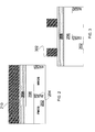
- a semiconductor substrate 202 is illustrated.
- the semiconductor substrate 202 includes shallow trench isolation (STI) features 204 formed therein.
- the STI features 204 may serve to isolate regions of the semiconductor substrate, as described above.
- STI feature 204 isolates a PMOS and NMOS region, however, any configuration is possible and within the scope of the present disclosure.
- a first layer 206 and a second layer 208 are formed on the substrate 202 .
- the first layer 206 is polysilicon.
- the second layer 208 is a hard mask.
- Example hard mask compositions include as silicon nitride (SiN) or silicon oxide (SiO 2 ). In the exemplary embodiment of FIG.
- the first and second layers 206 , 208 are target layers to be patterned (e.g., to form a gate structure).
- the first and second layers 206 , 208 have been patterned to form a gate structure 502 .
- the gate structure 502 is a dummy (e.g., sacrificial) gate used in a gate-replacement process (e.g., to form a metal gate of a transistor device).
- a photosensitive layer e.g., photoresist
- the photoresist layer may be formed using a spin-on coating process.
- the photoresist may be a negative or positive type photoresist of any suitable composition.
- the photoresist layer may be soft baked after its deposition. Referring to the example of FIGS. 2 and 5 respectively, a photoresist layer 210 layer is formed on the substrate 202 .
- the method 100 then proceeds to block 106 where an exposure process is performed on the photosensitive layer.
- the exposure process patterns the photosensitive layer.
- the exposure process may include introducing a radiation beam to the substrate.
- the radiation beam may be ultraviolet and/or can be extended to include other radiation beams such as ion beam, x-ray, extreme ultraviolet, deep ultraviolet, and other proper radiation energy.
- the exposure process may be part of an immersion lithography process, electron-bam writing, ion-beam writing, maskless photolithography, molecular imprint, and/or other suitable patterning processes.
- a post-exposure bake (PEB) may be performed to allow the exposed photoresist polymers to cleave.
- the exposed photosensitive layer is developed (e.g., a developer is applied to the patterned resist to remove the soluble portions of the layer).
- the substrate including the cleaved polymer photoresist is transferred to a developing chamber to remove portions of the photoresist (e.g., the exposed resist) that is soluble to an aqueous developer.
- the developer is tetra-methyl ammonium hydroxide (TMAH).
- TMAH tetra-methyl ammonium hydroxide
- a surfactant may also be included.
- the surfactant may selected from surfactants such as, 3M Novec fluid HFE-7000, HFE-7100, HFE-7200, HFE-7500, HFE-71IPA. 3M Fluorinert FC-72, FC-84, FC-77, FC-3255, FC-3283, FC-40, FC-43, FC-70. 3M Novec 4200, 3M Novec 4300, 3M FC-4432. 3M FC-4430, 3M FC-4434 and/or other surfactants known in the art.
- the developer may be applied by a puddling process, immersion, spray, and/or other suitable methods.
- the photosensitive layer has been patterned (e.g., exposed and developed) to form features 302 .
- the features 302 may be used as masking elements in the formation of a gate structure (e.g., a dummy gate structure).
- the photosensitive layer has been patterned to expose a portion of the substrate 202 (e.g., NMOS region), while a feature 602 of photoresist masks (protects) a second region (e.g., PMOS) of the substrate 202 .
- a hard mask layer e.g., second layer 208
- the patterned photoresist layer may be directly used as an etch mask to etch the gate material layers.
- the method 100 then proceeds to block 110 where a cleaning process is performed on the substrate, including the developed photosensitive layer.
- the cleaning process is performed in-situ with the development process, described above with reference to block 108 .
- the substrate is loaded in a chamber where it is exposed to a developer and subsequently to a rinse solution in a cleaning process before being removed from the chamber.
- the development and cleaning process may be performed in a development tool.
- the development tool may be a typical development tool that has been modified and/or other configured to perform the cleaning process including introducing a rinse solution.
- the rinse solution is a de-ionized water (DIW) and ozone (O 3 ) solution.
- An exemplary concentration of the DIW/O 3 rinse solution is between approximately 1 ppm and 500 ppm of ozone.
- the rinse solution is a DIW and hydrogen peroxide H 2 O 2 solution.
- An exemplary concentration of DIW/H 2 O 2 rinse solution is between approximately 0.1% and 10% by weight of H 2 O 2 .
- the rinse solution is a DIW and oxalic acid solution.
- An exemplary concentration of DIW/oxalic acid rinse solution is a concentration of oxalic acid between approximately 0.05% and 10% by weight.
- a trace amount of acid may be included in the rinse solution.
- the DIW/O 3 or DIW/H 2 O 2 solutions described above may include a trace amount of acid.
- the trace acid may be HCl, acetic acid, citric acid, tartaric acid, and/or other similar acids.
- the rinse solution includes between approximately 0.01 and approximately 10% by weight of HCl. In an embodiment, the rinse solution includes between approximately 0.01 and approximately 10% by weight of citric acid. In an embodiment, the rinse solution includes between approximately 0.01 and approximately 10% by weight of tartaric acid.
- An exemplary process temperature for the cleaning process is between approximately 10° C. and approximately 80° C.
- the rotational speed of the substrate during the rinse solution application may be between approximately 10 rpm and approximately 3000 rpm.
- the flowrate of the rinse solution may be between approximately 100 sccm and approximately 10 slm.
- the rinse solution such as described above is not applied in-situ.
- the substrate may be rinsed with DI water, baked, and then the above described cleaning process may be performed.
- the substrate may be dried, for example, using a spin-dry process.
- a hard bake process may be performed after the cleaning process.
- the method 100 may then proceed to subsequent steps in semiconductor fabrication.
- the photoresist features 302 may be used as masking elements to etch the first layer 206 and/or the second layer 208 .
- the gate structures 402 may be formed.
- the patterned photoresist layer 302 may be removed thereafter using a suitable process, such as wet stripping or plasma ashing.
- the cleaning process may provide an improvement of the LWR of the photoresist features 302 and thus, the LWR of the gate features 402 including the polysilicon layer 206 .
- the method 100 may proceed to include steps such as illustrated in FIG. 6 .
- an implantation process 604 may be performed on the device 600 .
- the implantation process may provide a portion (e.g., lightly doped source and drain (LDD)) of the source/drain of a device formed on the substrate 202 .
- the patterned photoresist layer 602 may be removed thereafter using a suitable process, such as wet stripping or plasma ashing.
- the device 600 may experience improvements over the conventional devices as the cleaning process may reduce and/or eliminate a residue of photosensitive material from the substrate 202 in regions denoted as 602 .
- FIGS. 2 , 3 , 4 , 5 , and 6 are exemplary only and not intended to be limiting.
- the method 100 including the cleaning process described above with reference to block 110 may performed during any stage of fabrication and in conjunction with any lithography process.
- a method 700 which is an embodiment of a photolithography method.
- the photolithography method 700 may be used to fabricate semiconductor devices including integrated circuits or portions thereof.
- the method 700 starts at block 702 where a substrate having a photosensitive layer disposed thereon is provided.
- Block 702 may be substantially similar to block 102 and/or 104 described above with reference to the method 100 of FIG. 1 .
- the method 700 then proceeds to block 704 where the photosensitive layer is exposed to a pattern.
- Block 704 may be substantially similar to block 106 , described above with reference to the method 100 of FIG. 1 .
- the method 700 then proceeds to block 706 where the substrate is loaded into a development chamber.
- the development chamber may be operable to introduce a developer (such as, TMAH) and a rinse solution to the substrate.
- the development chamber may include spray nozzles, spin-on coating mechanisms, mechanisms for puddle application of fluid, and/or other suitable application methods.
- the substrate may be loaded into the development chamber by manual or robotic means.
- the method 700 then proceeds to block 708 where the developer is applied to the substrate.
- the developer is TMAH.
- TMAH TMAH
- the developer may be selected based on the photosensitive layer composition.
- the developer may be applied by immersion of the substrate, spray application, puddle application, and/or other suitable application means.
- the method 700 then proceeds to block 710 where a rinse solution is applied to the substrate to perform a cleaning process.
- the rinse solution may be substantially similar to as discussed above with reference to block 110 of the method 100 .
- the rinse solution is applied in the same chamber as the developer of block 708 .
- no process steps are performed between the application of the developer and the application of the rinse solution.
- the rinse solution may be applied by immersion of the substrate, spray application, puddle application, and/or other suitable application means.
- the rinse solution is applied in the same manner as the developer solution.
- the rinse solution is a de-ionized water (DIW) and ozone (O 3 ) solution.
- DIW/O 3 rinse solution is between approximately 1 ppm and 500 ppm of ozone; the flowrate of the rinse solution may be between approximately 100 sccm and approximately 10 slm.
- the developer tool may be configured to provide a supply of ozone to the chamber.
- the rinse solution is a DIW and hydrogen peroxide H 2 O 2 solution.
- An exemplary concentration of DIW/H 2 O 2 rinse solution is between approximately 0.1% and 10% by weight of H 2 O 2 ; the flowrate of the rinse solution may be between approximately 100 sccm and approximately 10 slm.
- the developer tool may be configured to provide a supply of peroxide to the chamber.
- the rinse solution is a DIW and oxalic acid solution.
- An exemplary concentration of DIW/oxalic acid rinse solution is a concentration of oxalic acid between approximately 0.05% and 10% by weight; the flowrate of the rinse solution may be between approximately 100 sccm and approximately 10 slm.
- the developer tool may be configured to provide a supply of oxalic to the chamber.
- a trace amount of acid may be included in the rinse solution.
- the DIW/O 3 or DIW/H 2 O 2 solutions described above may include a trace amount of acid.
- the trace acid may be HCl, acetic acid, citric acid, tartaric acid, and/or other similar acids.
- the rinse solution includes between approximately 0.01 and approximately 10% by weight of HCl. In an embodiment, the rinse solution includes between approximately 0.01 and approximately 10% by weight of citric acid. In an embodiment, the rinse solution includes between approximately 0.01 and approximately 10% by weight of tartaric acid.
- the method 700 then proceeds to block 712 where the substrate is removed from the chamber.
- the substrate may be further processed including drying processes, hard bake processes, and/or other suitable processes.
- the rinse solution of the cleaning process includes DIW, and one or more additional components including H2O2, ozone, oxalic acid, and/or trace acids such as HCl, citric acid, acetic acid, and tartaric acid.
- One or more embodiments of the present disclosure may provide advantages such as, reduction of surfactant residue, improved LWR, reduction of photoresist residue and/or scum, and/or other benefits. Poor LWR can result in an impact on poly gate line width roughness, impact on the LDD implant profile, impact on the pocket implant profile, and/or influence of device performance such as, threshold voltage.
- Photoresist residue and/or scum can impact the LDD implant profile, impact the pocket implant profile, and/or influence the device performance such as threshold voltage.
- a surfactant residue can lead to issues such as photo corrosion, which in turn may cause an abnormal via profile, and/or other defects.
- a method of making an integrated circuit includes providing a substrate having a photosensitive layer.
- the photosensitive layer is exposed to a radiation beam.
- the exposed photosensitive layer is developed in a first chamber.
- a cleaning process is performed on the developed photosensitive layer.
- the cleaning process includes using a rinse solution including at least one of ozone, hydrogen peroxide, and oxalic acid.
- a method which also includes providing a semiconductor substrate.
- a developer is applied to the semiconductor substrate in a first chamber.
- a rinse solution is applied, after applying the developer, to the semiconductor substrate in the first chamber.
- the rinse solution includes at least one of ozone, hydrogen peroxide, and oxalic acid.
- the rinse solution further includes DIW.
- an acid is also included such as HCl, acetic acid, citric acid, and tartaric acid.
- a method of semiconductor fabrication includes providing a substrate having a photosensitive layer and exposing the photosensitive layer to a radiation beam. The exposed photosensitive layer is developed. A cleaning process is performed on the developed photosensitive layer. The cleaning process includes using a rinse solution including at least one of ozone, hydrogen peroxide, and oxalic acid.
Abstract
A method of making an integrated circuit is provided. The method includes providing a substrate having a photosensitive layer. The photosensitive layer is exposed to a radiation beam. The exposed photosensitive layer is developed in a first chamber. In the first chamber, a cleaning process is performed on the developed photosensitive layer. The cleaning process includes using a rinse solution including at least one of ozone, hydrogen peroxide, and oxalic acid.
Description
As the technology of semiconductor fabrication processes, the critical dimension (CD) has been reduced making lithography processes more and more challenging. Of particular importance is the control of line width roughness (LWR) or line edge roughness (LER). Line edge or width roughness generally refers to the roughness of a width or edge of a line of material in a semiconductor device (e.g., during fabrication). Uncontrolled LWR and LER can have a significant impact on the resulting semiconductor device (e.g., transistor). These impacts include parametric device performance and yield, for example, variations in critical dimension (CD) can cause variations is current (Ioff, Idsat). Other key concerns of the photolithography process include defects such as particles and water-marks. The conventional photolithography processes are typically insufficient to address these concerns. Therefore, a photolithography process and/or clean addressing the above issues is needed.
Aspects of the present disclosure are best understood from the following detailed description when read with the accompanying figures. It is emphasized that, in accordance with the standard practice in the industry, various features are not drawn to scale. In fact, the dimensions of the various features may be arbitrarily increased or reduced for clarity of discussion.
It is to be understood that the following disclosure provides many different embodiments, or examples, for implementing different features of various embodiments. Specific examples of components and arrangements are described below to simplify the present disclosure. These are, of course, merely examples and are not intended to be limiting. In addition, the present disclosure may repeat reference numerals and/or letters in the various examples. This repetition is for the purpose of simplicity and clarity and does not in itself dictate a relationship between the various embodiments and/or configurations discussed. Moreover, the formation of a first feature over or on a second feature in the description that follows may include embodiments in which the first and second features are formed in direct contact, and may also include embodiments in which additional features may be formed interposing the first and second features, such that the first and second features may not be in direct contact.
The present disclosure is directed, at times, to integrated circuit device manufacturing. However, one would recognize the benefits of the present disclosure can be applied in other device technologies, such as liquid crystal display (LCD) and/or any other technology which uses a photolithography process.
Referring to FIG. 1 , the method 100 begins at block 102 by providing a semiconductor substrate. The semiconductor substrate may have one or more layers (e.g., insulating layers, conductive layers, etc) formed thereon. The semiconductor substrate may include silicon. Alternatively, the substrate includes germanium, silicon germanium or other proper semiconductor materials. In one embodiment, the semiconductor substrate includes a first region (resistor region) for one or more semiconductor devices (e.g., FET) and a second region (device region) for one or more semiconductor devices (e.g., FET). Various STI features may be formed in the substrate. The formation of the STI features includes etching a trench in a substrate and filling the trench by one or more insulator materials such as silicon oxide, silicon nitride, or silicon oxynitride. The filled trench may have a multi-layer structure such as a thermal oxide liner layer with silicon nitride filling the trench. In one embodiment, the STI feature is created using a process sequence such as: growing a pad oxide, forming a low pressure chemical vapor deposition (LPCVD) nitride layer, patterning an STI opening using photoresist and masking, etching a trench in the substrate, optionally growing a thermal oxide trench liner to improve the trench interface, filling the trench with CVD oxide, using chemical mechanical planarization (CMP) to etch back, and using nitride stripping to leave the STI structure. The semiconductor substrate also includes various doped regions (e.g., n-wells and p-wells) formed in various active regions.
Referring to the example of FIGS. 2 and 5 , respectively. A semiconductor substrate 202 is illustrated. The semiconductor substrate 202 includes shallow trench isolation (STI) features 204 formed therein. The STI features 204 may serve to isolate regions of the semiconductor substrate, as described above. In the illustrated embodiments, STI feature 204 isolates a PMOS and NMOS region, however, any configuration is possible and within the scope of the present disclosure. A first layer 206 and a second layer 208 are formed on the substrate 202. In an embodiment, the first layer 206 is polysilicon. In an embodiment, the second layer 208 is a hard mask. Example hard mask compositions include as silicon nitride (SiN) or silicon oxide (SiO2). In the exemplary embodiment of FIG. 2 , the first and second layers 206, 208 are target layers to be patterned (e.g., to form a gate structure). In the exemplary embodiment of FIG. 5 , the first and second layers 206, 208 have been patterned to form a gate structure 502. In an embodiment, the gate structure 502 is a dummy (e.g., sacrificial) gate used in a gate-replacement process (e.g., to form a metal gate of a transistor device).
Referring again to FIG. 1 , the method 100 then proceeds to block 104 where a photosensitive layer (e.g., photoresist) is formed on the substrate. The photoresist layer may be formed using a spin-on coating process. The photoresist may be a negative or positive type photoresist of any suitable composition. The photoresist layer may be soft baked after its deposition. Referring to the example of FIGS. 2 and 5 respectively, a photoresist layer 210 layer is formed on the substrate 202.
The method 100 then proceeds to block 106 where an exposure process is performed on the photosensitive layer. The exposure process patterns the photosensitive layer. The exposure process may include introducing a radiation beam to the substrate. The radiation beam may be ultraviolet and/or can be extended to include other radiation beams such as ion beam, x-ray, extreme ultraviolet, deep ultraviolet, and other proper radiation energy. The exposure process may be part of an immersion lithography process, electron-bam writing, ion-beam writing, maskless photolithography, molecular imprint, and/or other suitable patterning processes. A post-exposure bake (PEB) may be performed to allow the exposed photoresist polymers to cleave.
The method then proceeds to block 108 where the exposed photosensitive layer is developed (e.g., a developer is applied to the patterned resist to remove the soluble portions of the layer). The substrate including the cleaved polymer photoresist is transferred to a developing chamber to remove portions of the photoresist (e.g., the exposed resist) that is soluble to an aqueous developer. In an embodiment, the developer is tetra-methyl ammonium hydroxide (TMAH). However, other compositions suitable compositions now known or later developed are also within the scope of the disclosure. A surfactant may also be included. The surfactant may selected from surfactants such as, 3M Novec fluid HFE-7000, HFE-7100, HFE-7200, HFE-7500, HFE-71IPA. 3M Fluorinert FC-72, FC-84, FC-77, FC-3255, FC-3283, FC-40, FC-43, FC-70. 3M Novec 4200, 3M Novec 4300, 3M FC-4432. 3M FC-4430, 3M FC-4434 and/or other surfactants known in the art. The developer may be applied by a puddling process, immersion, spray, and/or other suitable methods.
Referring to the example of FIG. 3 , the photosensitive layer has been patterned (e.g., exposed and developed) to form features 302. The features 302 may be used as masking elements in the formation of a gate structure (e.g., a dummy gate structure). Referring to the example of FIG. 6 , the photosensitive layer has been patterned to expose a portion of the substrate 202 (e.g., NMOS region), while a feature 602 of photoresist masks (protects) a second region (e.g., PMOS) of the substrate 202. Alternatively, if a hard mask layer (e.g., second layer 208) is not present, then the patterned photoresist layer may be directly used as an etch mask to etch the gate material layers.
Referring again to FIG. 1 , the method 100 then proceeds to block 110 where a cleaning process is performed on the substrate, including the developed photosensitive layer. In an embodiment, the cleaning process is performed in-situ with the development process, described above with reference to block 108. In other words, the substrate is loaded in a chamber where it is exposed to a developer and subsequently to a rinse solution in a cleaning process before being removed from the chamber. The development and cleaning process may be performed in a development tool. The development tool may be a typical development tool that has been modified and/or other configured to perform the cleaning process including introducing a rinse solution.
In an embodiment, the rinse solution is a de-ionized water (DIW) and ozone (O3) solution. An exemplary concentration of the DIW/O3 rinse solution is between approximately 1 ppm and 500 ppm of ozone. In an embodiment, the rinse solution is a DIW and hydrogen peroxide H2O2 solution. An exemplary concentration of DIW/H2O2 rinse solution is between approximately 0.1% and 10% by weight of H2O2. In an embodiment, the rinse solution is a DIW and oxalic acid solution. An exemplary concentration of DIW/oxalic acid rinse solution is a concentration of oxalic acid between approximately 0.05% and 10% by weight.
In further embodiments, a trace amount of acid may be included in the rinse solution. For example, the DIW/O3 or DIW/H2O2 solutions described above may include a trace amount of acid. The trace acid may be HCl, acetic acid, citric acid, tartaric acid, and/or other similar acids. In an embodiment, the rinse solution includes between approximately 0.01 and approximately 10% by weight of HCl. In an embodiment, the rinse solution includes between approximately 0.01 and approximately 10% by weight of citric acid. In an embodiment, the rinse solution includes between approximately 0.01 and approximately 10% by weight of tartaric acid.
The following process parameters are exemplary only and not intended to be limiting. An exemplary process temperature for the cleaning process is between approximately 10° C. and approximately 80° C. The rotational speed of the substrate during the rinse solution application may be between approximately 10 rpm and approximately 3000 rpm. The flowrate of the rinse solution may be between approximately 100 sccm and approximately 10 slm.
In an alternative embodiment, the rinse solution such as described above, is not applied in-situ. In an embodiment, after a development process, the substrate may be rinsed with DI water, baked, and then the above described cleaning process may be performed.
Following the cleaning process, the substrate may be dried, for example, using a spin-dry process. In some embodiment, a hard bake process may be performed after the cleaning process.
The method 100 may then proceed to subsequent steps in semiconductor fabrication. For example, in the exemplary embodiment of FIG. 4 , after the cleaning process, the photoresist features 302 may be used as masking elements to etch the first layer 206 and/or the second layer 208. Thus, the gate structures 402 may be formed. The patterned photoresist layer 302 may be removed thereafter using a suitable process, such as wet stripping or plasma ashing. It is noted that the device 400 may include several advantages over the prior art. For example, the cleaning process may provide an improvement of the LWR of the photoresist features 302 and thus, the LWR of the gate features 402 including the polysilicon layer 206.
As a further example, the method 100 may proceed to include steps such as illustrated in FIG. 6 . After the cleaning process, an implantation process 604 may be performed on the device 600. The implantation process may provide a portion (e.g., lightly doped source and drain (LDD)) of the source/drain of a device formed on the substrate 202. The patterned photoresist layer 602 may be removed thereafter using a suitable process, such as wet stripping or plasma ashing. The device 600 may experience improvements over the conventional devices as the cleaning process may reduce and/or eliminate a residue of photosensitive material from the substrate 202 in regions denoted as 602.
The embodiments of FIGS. 2,3, 4, 5, and 6 are exemplary only and not intended to be limiting. The method 100 including the cleaning process described above with reference to block 110 may performed during any stage of fabrication and in conjunction with any lithography process.
Referring now to FIG. 7 , illustrated is a method 700, which is an embodiment of a photolithography method. The photolithography method 700 may be used to fabricate semiconductor devices including integrated circuits or portions thereof. The method 700 starts at block 702 where a substrate having a photosensitive layer disposed thereon is provided. Block 702 may be substantially similar to block 102 and/or 104 described above with reference to the method 100 of FIG. 1 . The method 700 then proceeds to block 704 where the photosensitive layer is exposed to a pattern. Block 704 may be substantially similar to block 106, described above with reference to the method 100 of FIG. 1 .
The method 700 then proceeds to block 706 where the substrate is loaded into a development chamber. The development chamber may be operable to introduce a developer (such as, TMAH) and a rinse solution to the substrate. The development chamber may include spray nozzles, spin-on coating mechanisms, mechanisms for puddle application of fluid, and/or other suitable application methods. The substrate may be loaded into the development chamber by manual or robotic means.
The method 700 then proceeds to block 708 where the developer is applied to the substrate. In an embodiment, the developer is TMAH. However, one of ordinary skill in the art would recognize other developers, now known or later developed, that would be suitable for development of the exposed photosensitive layer. The developer may be selected based on the photosensitive layer composition. The developer may be applied by immersion of the substrate, spray application, puddle application, and/or other suitable application means.
The method 700 then proceeds to block 710 where a rinse solution is applied to the substrate to perform a cleaning process. The rinse solution may be substantially similar to as discussed above with reference to block 110 of the method 100. The rinse solution is applied in the same chamber as the developer of block 708. In an embodiment, no process steps are performed between the application of the developer and the application of the rinse solution. The rinse solution may be applied by immersion of the substrate, spray application, puddle application, and/or other suitable application means. In an embodiment, the rinse solution is applied in the same manner as the developer solution.
In an embodiment, the rinse solution is a de-ionized water (DIW) and ozone (O3) solution. An exemplary concentration of the DIW/O3 rinse solution is between approximately 1 ppm and 500 ppm of ozone; the flowrate of the rinse solution may be between approximately 100 sccm and approximately 10 slm. In the embodiment, the developer tool may be configured to provide a supply of ozone to the chamber. In an embodiment, the rinse solution is a DIW and hydrogen peroxide H2O2 solution. An exemplary concentration of DIW/H2O2 rinse solution is between approximately 0.1% and 10% by weight of H2O2; the flowrate of the rinse solution may be between approximately 100 sccm and approximately 10 slm. In the embodiment, the developer tool may be configured to provide a supply of peroxide to the chamber. In an embodiment, the rinse solution is a DIW and oxalic acid solution. An exemplary concentration of DIW/oxalic acid rinse solution is a concentration of oxalic acid between approximately 0.05% and 10% by weight; the flowrate of the rinse solution may be between approximately 100 sccm and approximately 10 slm. In the embodiment, the developer tool may be configured to provide a supply of oxalic to the chamber.
In further embodiments, a trace amount of acid may be included in the rinse solution. For example, the DIW/O3 or DIW/H2O2 solutions described above may include a trace amount of acid. The trace acid may be HCl, acetic acid, citric acid, tartaric acid, and/or other similar acids. In an embodiment, the rinse solution includes between approximately 0.01 and approximately 10% by weight of HCl. In an embodiment, the rinse solution includes between approximately 0.01 and approximately 10% by weight of citric acid. In an embodiment, the rinse solution includes between approximately 0.01 and approximately 10% by weight of tartaric acid.
The method 700 then proceeds to block 712 where the substrate is removed from the chamber. The substrate may be further processed including drying processes, hard bake processes, and/or other suitable processes.
Thus, provided is a method of semiconductor fabrication that includes a post-lithography cleaning process. The rinse solution of the cleaning process includes DIW, and one or more additional components including H2O2, ozone, oxalic acid, and/or trace acids such as HCl, citric acid, acetic acid, and tartaric acid. One or more embodiments of the present disclosure may provide advantages such as, reduction of surfactant residue, improved LWR, reduction of photoresist residue and/or scum, and/or other benefits. Poor LWR can result in an impact on poly gate line width roughness, impact on the LDD implant profile, impact on the pocket implant profile, and/or influence of device performance such as, threshold voltage. Photoresist residue and/or scum can impact the LDD implant profile, impact the pocket implant profile, and/or influence the device performance such as threshold voltage. A surfactant residue can lead to issues such as photo corrosion, which in turn may cause an abnormal via profile, and/or other defects.
The foregoing has outlined features of several embodiments. Those skilled in the art should appreciate that they may readily use the present disclosure as a basis for designing or modifying other processes and structures for carrying out the same purposes and/or achieving the same advantages of the embodiments introduced herein. Those skilled in the art should also realize that such equivalent constructions do not depart from the spirit and scope of the present disclosure, and that they may make various changes, substitutions and alterations herein without departing from the spirit and scope of the present disclosure.
Thus, in an embodiment, a method of making an integrated circuit is provided. The method includes providing a substrate having a photosensitive layer. The photosensitive layer is exposed to a radiation beam. The exposed photosensitive layer is developed in a first chamber. In the first chamber, a cleaning process is performed on the developed photosensitive layer. The cleaning process includes using a rinse solution including at least one of ozone, hydrogen peroxide, and oxalic acid.
In another embodiment, a method is provided which also includes providing a semiconductor substrate. A developer is applied to the semiconductor substrate in a first chamber. A rinse solution is applied, after applying the developer, to the semiconductor substrate in the first chamber. The rinse solution includes at least one of ozone, hydrogen peroxide, and oxalic acid. The rinse solution further includes DIW. In other embodiments, an acid is also included such as HCl, acetic acid, citric acid, and tartaric acid.
In yet another embodiment, a method of semiconductor fabrication includes providing a substrate having a photosensitive layer and exposing the photosensitive layer to a radiation beam. The exposed photosensitive layer is developed. A cleaning process is performed on the developed photosensitive layer. The cleaning process includes using a rinse solution including at least one of ozone, hydrogen peroxide, and oxalic acid.
Claims (18)
1. A method of making an integrated circuit, the method comprising:
providing a substrate having a photosensitive layer;
exposing the photosensitive layer to a radiation beam;
developing the exposed photosensitive layer, wherein the developing is performed in a first chamber; and
performing a cleaning process on the developed photosensitive layer, wherein the cleaning process is formed in the first chamber, and wherein the cleaning process includes using a rinse solution including at least one of ozone, hydrogen peroxide, and oxalic acid and another acid.
2. The method of claim 1 , wherein the rinse solution includes between approximately 1 ppm and approximately 500 ppm of ozone.
3. The method of claim 1 , wherein the rinse solution includes between approximately 0.1 weight percent and approximately 10 weight percent of hydrogen peroxide.
4. The method of claim 1 , wherein the rinse solution includes between approximately 0.05 weight percent and approximately 10 weight percent of oxalic acid.
5. The method of claim 1 , wherein the another acid is selected from the group consisting of HCl, acetic acid, citric acid, and tartaric acid.
6. The method of claim 1 , wherein the rinse solution includes between approximately 0.01 weight percent and approximately 10 weight percent of the another acid and the another acid is selected from the group consisting of HCl, acetic acid, citric acid, and tartaric acid.
7. The method of claim 1 , wherein the performing the cleaning process includes spraying the rinse solution onto the substrate.
8. The method of claim 1 , further comprising:
baking the substrate after performing the cleaning process.
9. The method of claim 1 , wherein the developing including providing tetra-methyl ammonium hydroxide (TMAH).
10. A method, the method comprising:
providing a semiconductor substrate;
applying a developer to the semiconductor substrate in a first chamber; and
applying a rinse solution, after applying the developer, to the semiconductor substrate in the first chamber, wherein the rinse solution includes a first component being at least one of ozone, hydrogen peroxide, and oxalic acid; a second component being another acid; and de-ionized water.
11. The method of claim 10 , wherein the rinse solution includes the first component of ozone.
12. The method of claim 10 , wherein the another acid of the rinse solution is selected from the group consisting of HCl, acetic acid, citric acid, and tartaric acid.
13. The method of claim 10 , wherein the rinse solution includes the first component of hydrogen peroxide.
14. The method of claim 10 ,
wherein the first component is hydrogen peroxide;
wherein the rinse solution includes at least approximately 0.1 weight percent (wt %) of the first component; and
wherein the rinse solution includes at least approximately 0.1 weight percent (wt %) of the another acid.
15. A method of semiconductor fabrication, comprising:
providing a substrate having a photosensitive layer;
exposing the photosensitive layer to a radiation beam;
developing the exposed photosensitive layer;
performing a cleaning process on the developed photosensitive layer, wherein the cleaning process includes using a rinse solution including oxalic acid;
performing a hard bake process on the cleaned and developed photosensitive layer to form a masking element in the photosensitive layer; and
using the masking element to pattern an underlying layer.
16. The method of claim 15 , further comprising:
a de-ionized water rinse prior to the cleaning process.
17. The method of claim 15 , wherein the rinse solution further comprises another acid, wherein the another acid is different from the oxalic acid.
18. The method of claim 15 , wherein the cleaning process is performed at a temperature between approximately 10° C. and approximately 80° C.
Priority Applications (1)
| Application Number | Priority Date | Filing Date | Title |
|---|---|---|---|
| US13/022,931 US8518634B2 (en) | 2011-02-08 | 2011-02-08 | Cleaning process for semiconductor device fabrication |
Applications Claiming Priority (1)
| Application Number | Priority Date | Filing Date | Title |
|---|---|---|---|
| US13/022,931 US8518634B2 (en) | 2011-02-08 | 2011-02-08 | Cleaning process for semiconductor device fabrication |
Publications (2)
| Publication Number | Publication Date |
|---|---|
| US20120202156A1 US20120202156A1 (en) | 2012-08-09 |
| US8518634B2 true US8518634B2 (en) | 2013-08-27 |
Family
ID=46600847
Family Applications (1)
| Application Number | Title | Priority Date | Filing Date |
|---|---|---|---|
| US13/022,931 Active 2031-08-12 US8518634B2 (en) | 2011-02-08 | 2011-02-08 | Cleaning process for semiconductor device fabrication |
Country Status (1)
| Country | Link |
|---|---|
| US (1) | US8518634B2 (en) |
Cited By (3)
| Publication number | Priority date | Publication date | Assignee | Title |
|---|---|---|---|---|
| US9529265B2 (en) | 2014-05-05 | 2016-12-27 | Taiwan Semiconductor Manufacturing Company, Ltd. | Method of preparing and using photosensitive material |
| US9919939B2 (en) | 2011-12-06 | 2018-03-20 | Delta Faucet Company | Ozone distribution in a faucet |
| US11458214B2 (en) | 2015-12-21 | 2022-10-04 | Delta Faucet Company | Fluid delivery system including a disinfectant device |
Families Citing this family (2)
| Publication number | Priority date | Publication date | Assignee | Title |
|---|---|---|---|---|
| JP6363431B2 (en) * | 2014-08-27 | 2018-07-25 | ルネサスエレクトロニクス株式会社 | Manufacturing method of semiconductor device |
| CN114351153A (en) * | 2021-12-27 | 2022-04-15 | 广东粤港澳大湾区国家纳米科技创新研究院 | Template cleaning agent and preparation method and application thereof |
Citations (9)
| Publication number | Priority date | Publication date | Assignee | Title |
|---|---|---|---|---|
| US5853961A (en) | 1995-04-19 | 1998-12-29 | Tokyo Electron Limited | Method of processing substrate and apparatus for processing substrate |
| US5887605A (en) | 1996-06-05 | 1999-03-30 | Samsung Electronics Co., Ltd. | Apparatus for cleaning semiconductor wafers |
| US6594847B1 (en) | 2000-03-28 | 2003-07-22 | Lam Research Corporation | Single wafer residue, thin film removal and clean |
| US6824621B2 (en) | 2001-06-22 | 2004-11-30 | S.E.S. Company Limited | Single wafer type substrate cleaning method and apparatus |
| US20080156346A1 (en) | 2006-12-28 | 2008-07-03 | Taiwan Semiconductor Manufacturing Company, Ltd. | Method and apparatus for cleaning a substrate |
| US20080166872A1 (en) * | 2005-08-10 | 2008-07-10 | Fujitsu Limited | Method of producing semiconductor device |
| US20090205677A1 (en) | 2002-04-11 | 2009-08-20 | Randhir Thakur | Method and apparatus for wafer cleaning |
| US20100104988A1 (en) * | 2002-01-28 | 2010-04-29 | Kabushiki Kaisha Toshiba | Substrate treating method, substrate-processing apparatus, developing method, method of manufacturing a semiconductor device, and method of cleaning a developing solution nozzle |
| US20100233449A1 (en) * | 2009-03-12 | 2010-09-16 | Renesas Technology Corp. | Method of forming resist pattern |
-
2011
- 2011-02-08 US US13/022,931 patent/US8518634B2/en active Active
Patent Citations (9)
| Publication number | Priority date | Publication date | Assignee | Title |
|---|---|---|---|---|
| US5853961A (en) | 1995-04-19 | 1998-12-29 | Tokyo Electron Limited | Method of processing substrate and apparatus for processing substrate |
| US5887605A (en) | 1996-06-05 | 1999-03-30 | Samsung Electronics Co., Ltd. | Apparatus for cleaning semiconductor wafers |
| US6594847B1 (en) | 2000-03-28 | 2003-07-22 | Lam Research Corporation | Single wafer residue, thin film removal and clean |
| US6824621B2 (en) | 2001-06-22 | 2004-11-30 | S.E.S. Company Limited | Single wafer type substrate cleaning method and apparatus |
| US20100104988A1 (en) * | 2002-01-28 | 2010-04-29 | Kabushiki Kaisha Toshiba | Substrate treating method, substrate-processing apparatus, developing method, method of manufacturing a semiconductor device, and method of cleaning a developing solution nozzle |
| US20090205677A1 (en) | 2002-04-11 | 2009-08-20 | Randhir Thakur | Method and apparatus for wafer cleaning |
| US20080166872A1 (en) * | 2005-08-10 | 2008-07-10 | Fujitsu Limited | Method of producing semiconductor device |
| US20080156346A1 (en) | 2006-12-28 | 2008-07-03 | Taiwan Semiconductor Manufacturing Company, Ltd. | Method and apparatus for cleaning a substrate |
| US20100233449A1 (en) * | 2009-03-12 | 2010-09-16 | Renesas Technology Corp. | Method of forming resist pattern |
Non-Patent Citations (4)
| Title |
|---|
| Dan Syverson; "Implant Stripping: Steam Injection for Uniform Wet Stripping;" 2010; Issue II; pp. 20-23; www.euroasiasemiconductor.com. |
| Manish Chandhok; Kent Frasure; E. Steve Putna; Todd R. Younkin; Willy Rachmady; Uday Shah and Wang Yueh; "Improvement in Linewidth Roughness by Postprocessing;" Nov./Dec. 2008; pp. 2265-2270; J. Vac. Sci. Technol. B 26(6); American Vacuum Society. |
| Ming-Hsi Yeh; Kuo-Sheng Chuang; Ying-Hsueh Chang Chien; Chi-Ming Yang and Chin-Hsiang Lin; "Semiconductor Device Cleaning Method and Apparatus;" U.S. Appl. No. 13/210,998, filed Aug. 16, 2011; 23 Pages. |
| Ming-Hsi Yeh; Kuo-Sheng Chuang; Ying-Hsueh Chien; Chi-Ming Yang; Chi-Wen Liu and Chin-Hsiang Lin; "Chemical Dispersion Method and Device;" U.S. Appl. No. 13/198,420, filed Aug. 4, 2011; 25 Pages. |
Cited By (4)
| Publication number | Priority date | Publication date | Assignee | Title |
|---|---|---|---|---|
| US9919939B2 (en) | 2011-12-06 | 2018-03-20 | Delta Faucet Company | Ozone distribution in a faucet |
| US10947138B2 (en) | 2011-12-06 | 2021-03-16 | Delta Faucet Company | Ozone distribution in a faucet |
| US9529265B2 (en) | 2014-05-05 | 2016-12-27 | Taiwan Semiconductor Manufacturing Company, Ltd. | Method of preparing and using photosensitive material |
| US11458214B2 (en) | 2015-12-21 | 2022-10-04 | Delta Faucet Company | Fluid delivery system including a disinfectant device |
Also Published As
| Publication number | Publication date |
|---|---|
| US20120202156A1 (en) | 2012-08-09 |
Similar Documents
| Publication | Publication Date | Title |
|---|---|---|
| JP5018307B2 (en) | Resist pattern thickening material, resist pattern forming method, semiconductor device and manufacturing method thereof | |
| KR102005640B1 (en) | Semiconductor method of protecting wafer from bevel contamination | |
| JP2010114414A (en) | Method of treating surface of semiconductor substrate | |
| US8822347B2 (en) | Wet soluble lithography | |
| US7410909B2 (en) | Method of removing ion implanted photoresist | |
| US8518634B2 (en) | Cleaning process for semiconductor device fabrication | |
| US10747114B2 (en) | Blocking layer material composition and methods thereof in semiconductor manufacturing | |
| CN106324998B (en) | The forming method of litho pattern | |
| US6764946B1 (en) | Method of controlling line edge roughness in resist films | |
| TWI725432B (en) | Lithography method | |
| JP2003068667A (en) | Production method for semiconductor device | |
| KR100761764B1 (en) | Method of removing a photoresist pattern, method of forming a dual polysilico layer ausing the same nd method of manufcaturing a semiconductor device using the same | |
| JP2001326173A (en) | Pattern-forming method | |
| KR100584498B1 (en) | Method for removing photoresist pattern | |
| CN117059482B (en) | Silicon dioxide wet etching method | |
| US8916052B2 (en) | Resist technique | |
| JP2006173260A (en) | Semiconductor device and manufacturing method therefor | |
| JP2011029562A (en) | Processing method of semiconductor-wafer end face, and manufacturing method of semiconductor device | |
| KR100608378B1 (en) | Method of forming recessed gate of semiconductor device | |
| TWI719083B (en) | Manufacturing method of semiconductor device | |
| KR100551336B1 (en) | Method for forming salicide of semiconductor device | |
| JP2004207590A (en) | Method of manufacturing semiconductor device | |
| KR100960483B1 (en) | Method for Manufacturing of Semiconductor Device | |
| KR20060054681A (en) | Method of forming photoresist pattern and layer pattern | |
| KR101096208B1 (en) | Method for forming isolation patterns of semiocnductor device |
Legal Events
| Date | Code | Title | Description |
|---|---|---|---|
| AS | Assignment |
Owner name: TAIWAN SEMICONDUCTOR MANUFACTURING COMPANY, LTD., Free format text: ASSIGNMENT OF ASSIGNORS INTEREST;ASSIGNORS:YEH, MING-HSI;LIN, YU-FU;KU, SHAO-YEN;AND OTHERS;SIGNING DATES FROM 20110210 TO 20110215;REEL/FRAME:025913/0559 |
|
| STCF | Information on status: patent grant |
Free format text: PATENTED CASE |
|
| FPAY | Fee payment |
Year of fee payment: 4 |
|
| MAFP | Maintenance fee payment |
Free format text: PAYMENT OF MAINTENANCE FEE, 8TH YEAR, LARGE ENTITY (ORIGINAL EVENT CODE: M1552); ENTITY STATUS OF PATENT OWNER: LARGE ENTITY Year of fee payment: 8 |