US8440520B2 - Diffused cap layers for modifying high-k gate dielectrics and interface layers - Google Patents
Diffused cap layers for modifying high-k gate dielectrics and interface layers Download PDFInfo
- Publication number
- US8440520B2 US8440520B2 US13/215,431 US201113215431A US8440520B2 US 8440520 B2 US8440520 B2 US 8440520B2 US 201113215431 A US201113215431 A US 201113215431A US 8440520 B2 US8440520 B2 US 8440520B2
- Authority
- US
- United States
- Prior art keywords
- film
- cap layer
- device region
- layer
- nmos
- Prior art date
- Legal status (The legal status is an assumption and is not a legal conclusion. Google has not performed a legal analysis and makes no representation as to the accuracy of the status listed.)
- Active
Links
- 239000003989 dielectric material Substances 0.000 title claims description 16
- 238000000034 method Methods 0.000 claims abstract description 145
- 239000000758 substrate Substances 0.000 claims abstract description 109
- 230000008569 process Effects 0.000 claims abstract description 91
- 229910052760 oxygen Inorganic materials 0.000 claims abstract description 54
- 239000001301 oxygen Substances 0.000 claims abstract description 54
- QVGXLLKOCUKJST-UHFFFAOYSA-N atomic oxygen Chemical compound [O] QVGXLLKOCUKJST-UHFFFAOYSA-N 0.000 claims abstract description 52
- 229910052729 chemical element Inorganic materials 0.000 claims abstract description 50
- 238000000151 deposition Methods 0.000 claims abstract description 42
- 238000009792 diffusion process Methods 0.000 claims abstract description 25
- 239000004065 semiconductor Substances 0.000 claims abstract description 18
- 229910052751 metal Inorganic materials 0.000 claims description 28
- 239000002184 metal Substances 0.000 claims description 28
- 229910052735 hafnium Inorganic materials 0.000 claims description 24
- VYPSYNLAJGMNEJ-UHFFFAOYSA-N Silicium dioxide Chemical compound O=[Si]=O VYPSYNLAJGMNEJ-UHFFFAOYSA-N 0.000 claims description 20
- 229910052726 zirconium Inorganic materials 0.000 claims description 18
- ATJFFYVFTNAWJD-UHFFFAOYSA-N Tin Chemical compound [Sn] ATJFFYVFTNAWJD-UHFFFAOYSA-N 0.000 claims description 17
- VBJZVLUMGGDVMO-UHFFFAOYSA-N hafnium atom Chemical compound [Hf] VBJZVLUMGGDVMO-UHFFFAOYSA-N 0.000 claims description 17
- 229910052746 lanthanum Inorganic materials 0.000 claims description 15
- 230000002000 scavenging effect Effects 0.000 claims description 15
- 229910052769 Ytterbium Inorganic materials 0.000 claims description 14
- 229910052688 Gadolinium Inorganic materials 0.000 claims description 13
- 229910052779 Neodymium Inorganic materials 0.000 claims description 13
- 229910052772 Samarium Inorganic materials 0.000 claims description 13
- 229910052771 Terbium Inorganic materials 0.000 claims description 13
- 229910052775 Thulium Inorganic materials 0.000 claims description 13
- 229910052727 yttrium Inorganic materials 0.000 claims description 13
- 229910052684 Cerium Inorganic materials 0.000 claims description 12
- 229910052692 Dysprosium Inorganic materials 0.000 claims description 12
- 229910052691 Erbium Inorganic materials 0.000 claims description 12
- 229910052693 Europium Inorganic materials 0.000 claims description 12
- 229910052689 Holmium Inorganic materials 0.000 claims description 12
- 229910052777 Praseodymium Inorganic materials 0.000 claims description 12
- 229910052782 aluminium Inorganic materials 0.000 claims description 12
- 229910004166 TaN Inorganic materials 0.000 claims description 8
- 229910004200 TaSiN Inorganic materials 0.000 claims description 8
- 229910008482 TiSiN Inorganic materials 0.000 claims description 8
- QRXWMOHMRWLFEY-UHFFFAOYSA-N isoniazide Chemical compound NNC(=O)C1=CC=NC=C1 QRXWMOHMRWLFEY-UHFFFAOYSA-N 0.000 claims description 8
- 239000000377 silicon dioxide Substances 0.000 claims description 8
- 229910052715 tantalum Inorganic materials 0.000 claims description 8
- 229910052681 coesite Inorganic materials 0.000 claims description 7
- 229910052906 cristobalite Inorganic materials 0.000 claims description 7
- 229910052682 stishovite Inorganic materials 0.000 claims description 7
- 229910052905 tridymite Inorganic materials 0.000 claims description 7
- 150000004767 nitrides Chemical class 0.000 claims description 6
- 229910052733 gallium Inorganic materials 0.000 claims description 5
- 229910004542 HfN Inorganic materials 0.000 claims description 4
- 229910015345 MOn Inorganic materials 0.000 claims description 4
- 229910000577 Silicon-germanium Inorganic materials 0.000 claims description 4
- 238000002955 isolation Methods 0.000 claims description 4
- 229910044991 metal oxide Inorganic materials 0.000 claims description 4
- 150000004706 metal oxides Chemical class 0.000 claims description 4
- 229910052750 molybdenum Inorganic materials 0.000 claims description 4
- 229910052697 platinum Inorganic materials 0.000 claims description 4
- 229910052702 rhenium Inorganic materials 0.000 claims description 4
- 229910052707 ruthenium Inorganic materials 0.000 claims description 4
- 229910052719 titanium Inorganic materials 0.000 claims description 4
- 239000010408 film Substances 0.000 description 194
- 239000007789 gas Substances 0.000 description 80
- 239000002243 precursor Substances 0.000 description 71
- 238000012545 processing Methods 0.000 description 53
- 230000004888 barrier function Effects 0.000 description 38
- 125000001449 isopropyl group Chemical group [H]C([H])([H])C([H])(*)C([H])([H])[H] 0.000 description 36
- -1 for example Substances 0.000 description 32
- ZSWFCLXCOIISFI-UHFFFAOYSA-N endo-cyclopentadiene Natural products C1C=CC=C1 ZSWFCLXCOIISFI-UHFFFAOYSA-N 0.000 description 31
- HPYIUKIBUJFXII-UHFFFAOYSA-N Cyclopentadienyl radical Chemical compound [CH]1C=CC=C1 HPYIUKIBUJFXII-UHFFFAOYSA-N 0.000 description 28
- XUIMIQQOPSSXEZ-UHFFFAOYSA-N Silicon Chemical compound [Si] XUIMIQQOPSSXEZ-UHFFFAOYSA-N 0.000 description 23
- 229910052710 silicon Inorganic materials 0.000 description 23
- 239000010703 silicon Substances 0.000 description 23
- 238000000231 atomic layer deposition Methods 0.000 description 22
- 125000000959 isobutyl group Chemical group [H]C([H])([H])C([H])(C([H])([H])[H])C([H])([H])* 0.000 description 17
- POILWHVDKZOXJZ-ARJAWSKDSA-M (z)-4-oxopent-2-en-2-olate Chemical compound C\C([O-])=C\C(C)=O POILWHVDKZOXJZ-ARJAWSKDSA-M 0.000 description 16
- 238000005229 chemical vapour deposition Methods 0.000 description 16
- 238000005530 etching Methods 0.000 description 16
- QUPDWYMUPZLYJZ-UHFFFAOYSA-N ethyl Chemical compound C[CH2] QUPDWYMUPZLYJZ-UHFFFAOYSA-N 0.000 description 16
- 239000003446 ligand Substances 0.000 description 16
- 239000000463 material Substances 0.000 description 15
- 238000000623 plasma-assisted chemical vapour deposition Methods 0.000 description 15
- 239000011777 magnesium Substances 0.000 description 14
- QJGQUHMNIGDVPM-UHFFFAOYSA-N nitrogen group Chemical group [N] QJGQUHMNIGDVPM-UHFFFAOYSA-N 0.000 description 14
- 239000011575 calcium Substances 0.000 description 13
- 230000010354 integration Effects 0.000 description 12
- DHHKPEUQJIEKOA-UHFFFAOYSA-N tert-butyl 2-[6-(nitromethyl)-6-bicyclo[3.2.0]hept-3-enyl]acetate Chemical compound C1C=CC2C(CC(=O)OC(C)(C)C)(C[N+]([O-])=O)CC21 DHHKPEUQJIEKOA-UHFFFAOYSA-N 0.000 description 12
- QCWXUUIWCKQGHC-UHFFFAOYSA-N Zirconium Chemical compound [Zr] QCWXUUIWCKQGHC-UHFFFAOYSA-N 0.000 description 11
- 150000001875 compounds Chemical class 0.000 description 11
- 229910052757 nitrogen Inorganic materials 0.000 description 10
- 238000010926 purge Methods 0.000 description 9
- 229910052761 rare earth metal Inorganic materials 0.000 description 9
- 150000002910 rare earth metals Chemical class 0.000 description 9
- 229910020751 SixGe1-x Inorganic materials 0.000 description 8
- 230000008021 deposition Effects 0.000 description 8
- 230000006870 function Effects 0.000 description 8
- 229910003443 lutetium oxide Inorganic materials 0.000 description 8
- MPARYNQUYZOBJM-UHFFFAOYSA-N oxo(oxolutetiooxy)lutetium Chemical compound O=[Lu]O[Lu]=O MPARYNQUYZOBJM-UHFFFAOYSA-N 0.000 description 8
- SIWVEOZUMHYXCS-UHFFFAOYSA-N oxo(oxoyttriooxy)yttrium Chemical compound O=[Y]O[Y]=O SIWVEOZUMHYXCS-UHFFFAOYSA-N 0.000 description 8
- 229920002120 photoresistant polymer Polymers 0.000 description 8
- 238000001039 wet etching Methods 0.000 description 8
- 125000000058 cyclopentadienyl group Chemical group C1(=CC=CC1)* 0.000 description 7
- 125000002496 methyl group Chemical group [H]C([H])([H])* 0.000 description 7
- 229910021420 polycrystalline silicon Inorganic materials 0.000 description 7
- 229910052712 strontium Inorganic materials 0.000 description 7
- 238000012546 transfer Methods 0.000 description 7
- QTBSBXVTEAMEQO-UHFFFAOYSA-N Acetic acid Chemical compound CC(O)=O QTBSBXVTEAMEQO-UHFFFAOYSA-N 0.000 description 6
- WEVYAHXRMPXWCK-UHFFFAOYSA-N Acetonitrile Chemical compound CC#N WEVYAHXRMPXWCK-UHFFFAOYSA-N 0.000 description 6
- RTZKZFJDLAIYFH-UHFFFAOYSA-N Diethyl ether Chemical compound CCOCC RTZKZFJDLAIYFH-UHFFFAOYSA-N 0.000 description 6
- YCKRFDGAMUMZLT-UHFFFAOYSA-N Fluorine atom Chemical compound [F] YCKRFDGAMUMZLT-UHFFFAOYSA-N 0.000 description 6
- 229910052581 Si3N4 Inorganic materials 0.000 description 6
- ZMANZCXQSJIPKH-UHFFFAOYSA-N Triethylamine Chemical compound CCN(CC)CC ZMANZCXQSJIPKH-UHFFFAOYSA-N 0.000 description 6
- 229910052788 barium Inorganic materials 0.000 description 6
- 229910052791 calcium Inorganic materials 0.000 description 6
- 239000000460 chlorine Substances 0.000 description 6
- 229910052731 fluorine Inorganic materials 0.000 description 6
- 239000011737 fluorine Substances 0.000 description 6
- INIGCWGJTZDVRY-UHFFFAOYSA-N hafnium zirconium Chemical compound [Zr].[Hf] INIGCWGJTZDVRY-UHFFFAOYSA-N 0.000 description 6
- 229910052749 magnesium Inorganic materials 0.000 description 6
- 230000001590 oxidative effect Effects 0.000 description 6
- 238000001020 plasma etching Methods 0.000 description 6
- HQVNEWCFYHHQES-UHFFFAOYSA-N silicon nitride Chemical compound N12[Si]34N5[Si]62N3[Si]51N64 HQVNEWCFYHHQES-UHFFFAOYSA-N 0.000 description 6
- 239000000126 substance Substances 0.000 description 6
- IJGRMHOSHXDMSA-UHFFFAOYSA-N Atomic nitrogen Chemical compound N#N IJGRMHOSHXDMSA-UHFFFAOYSA-N 0.000 description 5
- 229910015844 BCl3 Inorganic materials 0.000 description 5
- 150000004703 alkoxides Chemical class 0.000 description 5
- 125000000217 alkyl group Chemical group 0.000 description 5
- 150000001408 amides Chemical class 0.000 description 5
- 150000007942 carboxylates Chemical class 0.000 description 5
- 150000004820 halides Chemical class 0.000 description 5
- 239000012705 liquid precursor Substances 0.000 description 5
- 239000000203 mixture Substances 0.000 description 5
- 125000001181 organosilyl group Chemical group [SiH3]* 0.000 description 5
- FAQYAMRNWDIXMY-UHFFFAOYSA-N trichloroborane Chemical compound ClB(Cl)Cl FAQYAMRNWDIXMY-UHFFFAOYSA-N 0.000 description 5
- XLYOFNOQVPJJNP-UHFFFAOYSA-N water Substances O XLYOFNOQVPJJNP-UHFFFAOYSA-N 0.000 description 5
- ITWBWJFEJCHKSN-UHFFFAOYSA-N 1,4,7-triazonane Chemical compound C1CNCCNCCN1 ITWBWJFEJCHKSN-UHFFFAOYSA-N 0.000 description 4
- QGZKDVFQNNGYKY-UHFFFAOYSA-N Ammonia Chemical compound N QGZKDVFQNNGYKY-UHFFFAOYSA-N 0.000 description 4
- KZBUYRJDOAKODT-UHFFFAOYSA-N Chlorine Chemical compound ClCl KZBUYRJDOAKODT-UHFFFAOYSA-N 0.000 description 4
- ZAMOUSCENKQFHK-UHFFFAOYSA-N Chlorine atom Chemical compound [Cl] ZAMOUSCENKQFHK-UHFFFAOYSA-N 0.000 description 4
- XTHFKEDIFFGKHM-UHFFFAOYSA-N Dimethoxyethane Chemical compound COCCOC XTHFKEDIFFGKHM-UHFFFAOYSA-N 0.000 description 4
- OAKJQQAXSVQMHS-UHFFFAOYSA-N Hydrazine Chemical compound NN OAKJQQAXSVQMHS-UHFFFAOYSA-N 0.000 description 4
- NBIIXXVUZAFLBC-UHFFFAOYSA-N Phosphoric acid Chemical compound OP(O)(O)=O NBIIXXVUZAFLBC-UHFFFAOYSA-N 0.000 description 4
- JUJWROOIHBZHMG-UHFFFAOYSA-N Pyridine Chemical compound C1=CC=NC=C1 JUJWROOIHBZHMG-UHFFFAOYSA-N 0.000 description 4
- 229910006939 Si0.5Ge0.5 Inorganic materials 0.000 description 4
- 229910004491 TaAlN Inorganic materials 0.000 description 4
- WYURNTSHIVDZCO-UHFFFAOYSA-N Tetrahydrofuran Chemical compound C1CCOC1 WYURNTSHIVDZCO-UHFFFAOYSA-N 0.000 description 4
- 229910010037 TiAlN Inorganic materials 0.000 description 4
- RTAQQCXQSZGOHL-UHFFFAOYSA-N Titanium Chemical compound [Ti] RTAQQCXQSZGOHL-UHFFFAOYSA-N 0.000 description 4
- 150000001412 amines Chemical class 0.000 description 4
- 229910021417 amorphous silicon Inorganic materials 0.000 description 4
- DSAJWYNOEDNPEQ-UHFFFAOYSA-N barium atom Chemical compound [Ba] DSAJWYNOEDNPEQ-UHFFFAOYSA-N 0.000 description 4
- 229910002113 barium titanate Inorganic materials 0.000 description 4
- UORVGPXVDQYIDP-UHFFFAOYSA-N borane Chemical compound B UORVGPXVDQYIDP-UHFFFAOYSA-N 0.000 description 4
- 229910052801 chlorine Inorganic materials 0.000 description 4
- 239000002131 composite material Substances 0.000 description 4
- 150000003983 crown ethers Chemical class 0.000 description 4
- 239000002019 doping agent Substances 0.000 description 4
- 230000008030 elimination Effects 0.000 description 4
- 238000003379 elimination reaction Methods 0.000 description 4
- 238000005516 engineering process Methods 0.000 description 4
- 150000002170 ethers Chemical class 0.000 description 4
- 229940052303 ethers for general anesthesia Drugs 0.000 description 4
- 230000005669 field effect Effects 0.000 description 4
- 239000012212 insulator Substances 0.000 description 4
- FZLIPJUXYLNCLC-UHFFFAOYSA-N lanthanum atom Chemical compound [La] FZLIPJUXYLNCLC-UHFFFAOYSA-N 0.000 description 4
- 239000007788 liquid Substances 0.000 description 4
- 125000004108 n-butyl group Chemical group [H]C([H])([H])C([H])([H])C([H])([H])C([H])([H])* 0.000 description 4
- RVTZCBVAJQQJTK-UHFFFAOYSA-N oxygen(2-);zirconium(4+) Chemical compound [O-2].[O-2].[Zr+4] RVTZCBVAJQQJTK-UHFFFAOYSA-N 0.000 description 4
- NFHFRUOZVGFOOS-UHFFFAOYSA-N palladium;triphenylphosphane Chemical compound [Pd].C1=CC=CC=C1P(C=1C=CC=CC=1)C1=CC=CC=C1.C1=CC=CC=C1P(C=1C=CC=CC=1)C1=CC=CC=C1.C1=CC=CC=C1P(C=1C=CC=CC=1)C1=CC=CC=C1.C1=CC=CC=C1P(C=1C=CC=CC=1)C1=CC=CC=C1 NFHFRUOZVGFOOS-UHFFFAOYSA-N 0.000 description 4
- 229910001404 rare earth metal oxide Inorganic materials 0.000 description 4
- 230000009467 reduction Effects 0.000 description 4
- 125000002914 sec-butyl group Chemical group [H]C([H])([H])C([H])([H])C([H])(*)C([H])([H])[H] 0.000 description 4
- 238000000926 separation method Methods 0.000 description 4
- 229910052814 silicon oxide Inorganic materials 0.000 description 4
- 238000004544 sputter deposition Methods 0.000 description 4
- CIOAGBVUUVVLOB-UHFFFAOYSA-N strontium atom Chemical compound [Sr] CIOAGBVUUVVLOB-UHFFFAOYSA-N 0.000 description 4
- 229910003468 tantalcarbide Inorganic materials 0.000 description 4
- ZUHZGEOKBKGPSW-UHFFFAOYSA-N tetraglyme Chemical compound COCCOCCOCCOCCOC ZUHZGEOKBKGPSW-UHFFFAOYSA-N 0.000 description 4
- GETQZCLCWQTVFV-UHFFFAOYSA-N trimethylamine Chemical compound CN(C)C GETQZCLCWQTVFV-UHFFFAOYSA-N 0.000 description 4
- 229910001928 zirconium oxide Inorganic materials 0.000 description 4
- RHUYHJGZWVXEHW-UHFFFAOYSA-N 1,1-Dimethyhydrazine Chemical compound CN(C)N RHUYHJGZWVXEHW-UHFFFAOYSA-N 0.000 description 3
- ZYVYEJXMYBUCMN-UHFFFAOYSA-N 1-methoxy-2-methylpropane Chemical compound COCC(C)C ZYVYEJXMYBUCMN-UHFFFAOYSA-N 0.000 description 3
- OYPRJOBELJOOCE-UHFFFAOYSA-N Calcium Chemical compound [Ca] OYPRJOBELJOOCE-UHFFFAOYSA-N 0.000 description 3
- 229910052765 Lutetium Inorganic materials 0.000 description 3
- FYYHWMGAXLPEAU-UHFFFAOYSA-N Magnesium Chemical compound [Mg] FYYHWMGAXLPEAU-UHFFFAOYSA-N 0.000 description 3
- CBENFWSGALASAD-UHFFFAOYSA-N Ozone Chemical compound [O-][O+]=O CBENFWSGALASAD-UHFFFAOYSA-N 0.000 description 3
- XAGFODPZIPBFFR-UHFFFAOYSA-N aluminium Chemical compound [Al] XAGFODPZIPBFFR-UHFFFAOYSA-N 0.000 description 3
- 125000000129 anionic group Chemical group 0.000 description 3
- 229910052790 beryllium Inorganic materials 0.000 description 3
- ATBAMAFKBVZNFJ-UHFFFAOYSA-N beryllium atom Chemical compound [Be] ATBAMAFKBVZNFJ-UHFFFAOYSA-N 0.000 description 3
- 229910000085 borane Inorganic materials 0.000 description 3
- GWXLDORMOJMVQZ-UHFFFAOYSA-N cerium Chemical compound [Ce] GWXLDORMOJMVQZ-UHFFFAOYSA-N 0.000 description 3
- DWCMDRNGBIZOQL-UHFFFAOYSA-N dimethylazanide;zirconium(4+) Chemical compound [Zr+4].C[N-]C.C[N-]C.C[N-]C.C[N-]C DWCMDRNGBIZOQL-UHFFFAOYSA-N 0.000 description 3
- KBQHZAAAGSGFKK-UHFFFAOYSA-N dysprosium atom Chemical compound [Dy] KBQHZAAAGSGFKK-UHFFFAOYSA-N 0.000 description 3
- UYAHIZSMUZPPFV-UHFFFAOYSA-N erbium Chemical compound [Er] UYAHIZSMUZPPFV-UHFFFAOYSA-N 0.000 description 3
- OGPBJKLSAFTDLK-UHFFFAOYSA-N europium atom Chemical compound [Eu] OGPBJKLSAFTDLK-UHFFFAOYSA-N 0.000 description 3
- 150000002240 furans Chemical class 0.000 description 3
- UIWYJDYFSGRHKR-UHFFFAOYSA-N gadolinium atom Chemical compound [Gd] UIWYJDYFSGRHKR-UHFFFAOYSA-N 0.000 description 3
- 238000010438 heat treatment Methods 0.000 description 3
- KJZYNXUDTRRSPN-UHFFFAOYSA-N holmium atom Chemical compound [Ho] KJZYNXUDTRRSPN-UHFFFAOYSA-N 0.000 description 3
- 239000011261 inert gas Substances 0.000 description 3
- 238000002347 injection Methods 0.000 description 3
- 239000007924 injection Substances 0.000 description 3
- OHSVLFRHMCKCQY-UHFFFAOYSA-N lutetium atom Chemical compound [Lu] OHSVLFRHMCKCQY-UHFFFAOYSA-N 0.000 description 3
- 238000004519 manufacturing process Methods 0.000 description 3
- 125000004123 n-propyl group Chemical group [H]C([H])([H])C([H])([H])C([H])([H])* 0.000 description 3
- QEFYFXOXNSNQGX-UHFFFAOYSA-N neodymium atom Chemical compound [Nd] QEFYFXOXNSNQGX-UHFFFAOYSA-N 0.000 description 3
- 230000007935 neutral effect Effects 0.000 description 3
- 150000002825 nitriles Chemical class 0.000 description 3
- 229910052756 noble gas Inorganic materials 0.000 description 3
- 230000003647 oxidation Effects 0.000 description 3
- 238000007254 oxidation reaction Methods 0.000 description 3
- 230000000737 periodic effect Effects 0.000 description 3
- 229920005591 polysilicon Polymers 0.000 description 3
- PUDIUYLPXJFUGB-UHFFFAOYSA-N praseodymium atom Chemical compound [Pr] PUDIUYLPXJFUGB-UHFFFAOYSA-N 0.000 description 3
- 238000005086 pumping Methods 0.000 description 3
- 150000003222 pyridines Chemical class 0.000 description 3
- 150000003235 pyrrolidines Chemical class 0.000 description 3
- KZUNJOHGWZRPMI-UHFFFAOYSA-N samarium atom Chemical compound [Sm] KZUNJOHGWZRPMI-UHFFFAOYSA-N 0.000 description 3
- 239000007787 solid Substances 0.000 description 3
- 239000000243 solution Substances 0.000 description 3
- GZCRRIHWUXGPOV-UHFFFAOYSA-N terbium atom Chemical compound [Tb] GZCRRIHWUXGPOV-UHFFFAOYSA-N 0.000 description 3
- FRNOGLGSGLTDKL-UHFFFAOYSA-N thulium atom Chemical compound [Tm] FRNOGLGSGLTDKL-UHFFFAOYSA-N 0.000 description 3
- 230000008016 vaporization Effects 0.000 description 3
- NAWDYIZEMPQZHO-UHFFFAOYSA-N ytterbium Chemical compound [Yb] NAWDYIZEMPQZHO-UHFFFAOYSA-N 0.000 description 3
- VWQVUPCCIRVNHF-UHFFFAOYSA-N yttrium atom Chemical compound [Y] VWQVUPCCIRVNHF-UHFFFAOYSA-N 0.000 description 3
- DIIIISSCIXVANO-UHFFFAOYSA-N 1,2-Dimethylhydrazine Chemical compound CNNC DIIIISSCIXVANO-UHFFFAOYSA-N 0.000 description 2
- AVFZOVWCLRSYKC-UHFFFAOYSA-N 1-methylpyrrolidine Chemical compound CN1CCCC1 AVFZOVWCLRSYKC-UHFFFAOYSA-N 0.000 description 2
- AOPDRZXCEAKHHW-UHFFFAOYSA-N 1-pentoxypentane Chemical compound CCCCCOCCCCC AOPDRZXCEAKHHW-UHFFFAOYSA-N 0.000 description 2
- BPRYUXCVCCNUFE-UHFFFAOYSA-M 2,4,6-trimethylphenolate Chemical compound CC1=CC(C)=C([O-])C(C)=C1 BPRYUXCVCCNUFE-UHFFFAOYSA-M 0.000 description 2
- OBETXYAYXDNJHR-UHFFFAOYSA-N 2-Ethylhexanoic acid Chemical group CCCCC(CC)C(O)=O OBETXYAYXDNJHR-UHFFFAOYSA-N 0.000 description 2
- SDTMFDGELKWGFT-UHFFFAOYSA-N 2-methylpropan-2-olate Chemical compound CC(C)(C)[O-] SDTMFDGELKWGFT-UHFFFAOYSA-N 0.000 description 2
- VHUUQVKOLVNVRT-UHFFFAOYSA-N Ammonium hydroxide Chemical compound [NH4+].[OH-] VHUUQVKOLVNVRT-UHFFFAOYSA-N 0.000 description 2
- CPELXLSAUQHCOX-UHFFFAOYSA-M Bromide Chemical compound [Br-] CPELXLSAUQHCOX-UHFFFAOYSA-M 0.000 description 2
- VEXZGXHMUGYJMC-UHFFFAOYSA-M Chloride anion Chemical compound [Cl-] VEXZGXHMUGYJMC-UHFFFAOYSA-M 0.000 description 2
- KRHYYFGTRYWZRS-UHFFFAOYSA-M Fluoride anion Chemical compound [F-] KRHYYFGTRYWZRS-UHFFFAOYSA-M 0.000 description 2
- 229910001218 Gallium arsenide Inorganic materials 0.000 description 2
- 229910003946 H3Si Inorganic materials 0.000 description 2
- 229910004129 HfSiO Inorganic materials 0.000 description 2
- 229910000673 Indium arsenide Inorganic materials 0.000 description 2
- AHVYPIQETPWLSZ-UHFFFAOYSA-N N-methyl-pyrrolidine Natural products CN1CC=CC1 AHVYPIQETPWLSZ-UHFFFAOYSA-N 0.000 description 2
- BIVNKSDKIFWKFA-UHFFFAOYSA-N N-propan-2-yl-N-silylpropan-2-amine Chemical compound CC(C)N([SiH3])C(C)C BIVNKSDKIFWKFA-UHFFFAOYSA-N 0.000 description 2
- DBDXIWLGPZEGOL-UHFFFAOYSA-N N-tert-butyl-2-methylpropan-2-amine [dimethyl-(trimethylsilylamino)silyl]methane Chemical compound CC(C)(C)NC(C)(C)C.C[Si](C)(C)N[Si](C)(C)C DBDXIWLGPZEGOL-UHFFFAOYSA-N 0.000 description 2
- GRYLNZFGIOXLOG-UHFFFAOYSA-N Nitric acid Chemical compound O[N+]([O-])=O GRYLNZFGIOXLOG-UHFFFAOYSA-N 0.000 description 2
- BPQQTUXANYXVAA-UHFFFAOYSA-N Orthosilicate Chemical compound [O-][Si]([O-])([O-])[O-] BPQQTUXANYXVAA-UHFFFAOYSA-N 0.000 description 2
- 229910052773 Promethium Inorganic materials 0.000 description 2
- 229910003811 SiGeC Inorganic materials 0.000 description 2
- BLRPTPMANUNPDV-UHFFFAOYSA-N Silane Chemical compound [SiH4] BLRPTPMANUNPDV-UHFFFAOYSA-N 0.000 description 2
- 229910006501 ZrSiO Inorganic materials 0.000 description 2
- OLBVUFHMDRJKTK-UHFFFAOYSA-N [N].[O] Chemical compound [N].[O] OLBVUFHMDRJKTK-UHFFFAOYSA-N 0.000 description 2
- CEPICIBPGDWCRU-UHFFFAOYSA-N [Si].[Hf] Chemical compound [Si].[Hf] CEPICIBPGDWCRU-UHFFFAOYSA-N 0.000 description 2
- RFBRDHGMLHXGOB-UHFFFAOYSA-N [Si].[Zr].[Hf] Chemical compound [Si].[Zr].[Hf] RFBRDHGMLHXGOB-UHFFFAOYSA-N 0.000 description 2
- 229910000147 aluminium phosphate Inorganic materials 0.000 description 2
- 238000004380 ashing Methods 0.000 description 2
- 229910052454 barium strontium titanate Inorganic materials 0.000 description 2
- JRPBQTZRNDNNOP-UHFFFAOYSA-N barium titanate Chemical compound [Ba+2].[Ba+2].[O-][Ti]([O-])([O-])[O-] JRPBQTZRNDNNOP-UHFFFAOYSA-N 0.000 description 2
- 230000005540 biological transmission Effects 0.000 description 2
- 230000015572 biosynthetic process Effects 0.000 description 2
- 229910052796 boron Inorganic materials 0.000 description 2
- 230000005587 bubbling Effects 0.000 description 2
- 239000000872 buffer Substances 0.000 description 2
- 125000000484 butyl group Chemical group [H]C([*])([H])C([H])([H])C([H])([H])C([H])([H])[H] 0.000 description 2
- SHZIWNPUGXLXDT-UHFFFAOYSA-N caproic acid ethyl ester Natural products CCCCCC(=O)OCC SHZIWNPUGXLXDT-UHFFFAOYSA-N 0.000 description 2
- 238000007796 conventional method Methods 0.000 description 2
- 238000001816 cooling Methods 0.000 description 2
- 230000007547 defect Effects 0.000 description 2
- 229960004132 diethyl ether Drugs 0.000 description 2
- UCXUKTLCVSGCNR-UHFFFAOYSA-N diethylsilane Chemical compound CC[SiH2]CC UCXUKTLCVSGCNR-UHFFFAOYSA-N 0.000 description 2
- SBZXBUIDTXKZTM-UHFFFAOYSA-N diglyme Chemical compound COCCOCCOC SBZXBUIDTXKZTM-UHFFFAOYSA-N 0.000 description 2
- 230000002708 enhancing effect Effects 0.000 description 2
- HHFAWKCIHAUFRX-UHFFFAOYSA-N ethoxide Chemical compound CC[O-] HHFAWKCIHAUFRX-UHFFFAOYSA-N 0.000 description 2
- KQHQLIAOAVMAOW-UHFFFAOYSA-N hafnium(4+) oxygen(2-) zirconium(4+) Chemical compound [O--].[O--].[O--].[O--].[Zr+4].[Hf+4] KQHQLIAOAVMAOW-UHFFFAOYSA-N 0.000 description 2
- CJNBYAVZURUTKZ-UHFFFAOYSA-N hafnium(iv) oxide Chemical compound O=[Hf]=O CJNBYAVZURUTKZ-UHFFFAOYSA-N 0.000 description 2
- 229910052734 helium Inorganic materials 0.000 description 2
- XMBWDFGMSWQBCA-UHFFFAOYSA-N hydrogen iodide Chemical compound I XMBWDFGMSWQBCA-UHFFFAOYSA-N 0.000 description 2
- RPQDHPTXJYYUPQ-UHFFFAOYSA-N indium arsenide Chemical compound [In]#[As] RPQDHPTXJYYUPQ-UHFFFAOYSA-N 0.000 description 2
- PSCMQHVBLHHWTO-UHFFFAOYSA-K indium(iii) chloride Chemical compound Cl[In](Cl)Cl PSCMQHVBLHHWTO-UHFFFAOYSA-K 0.000 description 2
- 238000009616 inductively coupled plasma Methods 0.000 description 2
- 239000006193 liquid solution Substances 0.000 description 2
- 238000001459 lithography Methods 0.000 description 2
- 150000002739 metals Chemical class 0.000 description 2
- 229910003465 moissanite Inorganic materials 0.000 description 2
- 229910021421 monocrystalline silicon Inorganic materials 0.000 description 2
- HDZGCSFEDULWCS-UHFFFAOYSA-N monomethylhydrazine Chemical compound CNN HDZGCSFEDULWCS-UHFFFAOYSA-N 0.000 description 2
- SSCVMVQLICADPI-UHFFFAOYSA-N n-methyl-n-[tris(dimethylamino)silyl]methanamine Chemical compound CN(C)[Si](N(C)C)(N(C)C)N(C)C SSCVMVQLICADPI-UHFFFAOYSA-N 0.000 description 2
- 229910017604 nitric acid Inorganic materials 0.000 description 2
- 229910000069 nitrogen hydride Inorganic materials 0.000 description 2
- 230000003287 optical effect Effects 0.000 description 2
- 150000002926 oxygen Chemical class 0.000 description 2
- 125000002097 pentamethylcyclopentadienyl group Chemical group 0.000 description 2
- ISWSIDIOOBJBQZ-UHFFFAOYSA-M phenolate Chemical compound [O-]C1=CC=CC=C1 ISWSIDIOOBJBQZ-UHFFFAOYSA-M 0.000 description 2
- 238000000206 photolithography Methods 0.000 description 2
- JAMNHZBIQDNHMM-UHFFFAOYSA-N pivalonitrile Chemical compound CC(C)(C)C#N JAMNHZBIQDNHMM-UHFFFAOYSA-N 0.000 description 2
- VQMWBBYLQSCNPO-UHFFFAOYSA-N promethium atom Chemical compound [Pm] VQMWBBYLQSCNPO-UHFFFAOYSA-N 0.000 description 2
- OGHBATFHNDZKSO-UHFFFAOYSA-N propan-2-olate Chemical compound CC(C)[O-] OGHBATFHNDZKSO-UHFFFAOYSA-N 0.000 description 2
- UMJSCPRVCHMLSP-UHFFFAOYSA-N pyridine Natural products COC1=CC=CN=C1 UMJSCPRVCHMLSP-UHFFFAOYSA-N 0.000 description 2
- 239000000376 reactant Substances 0.000 description 2
- 125000001339 silanediyl group Chemical group [H][Si]([H])(*)* 0.000 description 2
- 229910010271 silicon carbide Inorganic materials 0.000 description 2
- 239000012686 silicon precursor Substances 0.000 description 2
- UVGLBOPDEUYYCS-UHFFFAOYSA-N silicon zirconium Chemical compound [Si].[Zr] UVGLBOPDEUYYCS-UHFFFAOYSA-N 0.000 description 2
- 125000003808 silyl group Chemical group [H][Si]([H])([H])[*] 0.000 description 2
- 239000002904 solvent Substances 0.000 description 2
- VEALVRVVWBQVSL-UHFFFAOYSA-N strontium titanate Chemical compound [Sr+2].[O-][Ti]([O-])=O VEALVRVVWBQVSL-UHFFFAOYSA-N 0.000 description 2
- YLQBMQCUIZJEEH-UHFFFAOYSA-N tetrahydrofuran Natural products C=1C=COC=1 YLQBMQCUIZJEEH-UHFFFAOYSA-N 0.000 description 2
- LXEXBJXDGVGRAR-UHFFFAOYSA-N trichloro(trichlorosilyl)silane Chemical compound Cl[Si](Cl)(Cl)[Si](Cl)(Cl)Cl LXEXBJXDGVGRAR-UHFFFAOYSA-N 0.000 description 2
- LALRXNPLTWZJIJ-UHFFFAOYSA-N triethylborane Chemical compound CCB(CC)CC LALRXNPLTWZJIJ-UHFFFAOYSA-N 0.000 description 2
- YFNKIDBQEZZDLK-UHFFFAOYSA-N triglyme Chemical compound COCCOCCOCCOC YFNKIDBQEZZDLK-UHFFFAOYSA-N 0.000 description 2
- 125000000026 trimethylsilyl group Chemical group [H]C([H])([H])[Si]([*])(C([H])([H])[H])C([H])([H])[H] 0.000 description 2
- 238000009834 vaporization Methods 0.000 description 2
- 239000006200 vaporizer Substances 0.000 description 2
- GFQYVLUOOAAOGM-UHFFFAOYSA-N zirconium(iv) silicate Chemical compound [Zr+4].[O-][Si]([O-])([O-])[O-] GFQYVLUOOAAOGM-UHFFFAOYSA-N 0.000 description 2
- JOMDRFHDFPOLDV-VNGPFPIXSA-K (Z)-6,6,7,7,8,8,8-heptafluoro-2,2-dimethyl-5-oxooct-3-en-3-olate lanthanum(3+) Chemical compound [La+3].CC(C)(C)C(\[O-])=C\C(=O)C(F)(F)C(F)(F)C(F)(F)F.CC(C)(C)C(\[O-])=C\C(=O)C(F)(F)C(F)(F)C(F)(F)F.CC(C)(C)C(\[O-])=C\C(=O)C(F)(F)C(F)(F)C(F)(F)F JOMDRFHDFPOLDV-VNGPFPIXSA-K 0.000 description 1
- KZBQCXBCJMHJOB-VNGPFPIXSA-K (z)-6,6,7,7,8,8,8-heptafluoro-2,2-dimethyl-5-oxooct-3-en-3-olate;ytterbium(3+) Chemical compound [Yb+3].CC(C)(C)C(\[O-])=C\C(=O)C(F)(F)C(F)(F)C(F)(F)F.CC(C)(C)C(\[O-])=C\C(=O)C(F)(F)C(F)(F)C(F)(F)F.CC(C)(C)C(\[O-])=C\C(=O)C(F)(F)C(F)(F)C(F)(F)F KZBQCXBCJMHJOB-VNGPFPIXSA-K 0.000 description 1
- ZKRDKPISZHQYEL-UHFFFAOYSA-N 2-bis(2,2-dimethylhydrazinyl)silyl-1,1-dimethylhydrazine Chemical compound CN(C)N[SiH](NN(C)C)NN(C)C ZKRDKPISZHQYEL-UHFFFAOYSA-N 0.000 description 1
- BGGIUGXMWNKMCP-UHFFFAOYSA-N 2-methylpropan-2-olate;zirconium(4+) Chemical compound CC(C)(C)O[Zr](OC(C)(C)C)(OC(C)(C)C)OC(C)(C)C BGGIUGXMWNKMCP-UHFFFAOYSA-N 0.000 description 1
- BSYNRYMUTXBXSQ-UHFFFAOYSA-N Aspirin Chemical compound CC(=O)OC1=CC=CC=C1C(O)=O BSYNRYMUTXBXSQ-UHFFFAOYSA-N 0.000 description 1
- ZOXJGFHDIHLPTG-UHFFFAOYSA-N Boron Chemical compound [B] ZOXJGFHDIHLPTG-UHFFFAOYSA-N 0.000 description 1
- 239000012695 Ce precursor Substances 0.000 description 1
- 229910005267 GaCl3 Inorganic materials 0.000 description 1
- 229910003865 HfCl4 Inorganic materials 0.000 description 1
- 101100521334 Mus musculus Prom1 gene Proteins 0.000 description 1
- AAIOMABGQIWKQQ-UHFFFAOYSA-N N-[di(propan-2-yl)amino]silyl-N-propan-2-ylpropan-2-amine Chemical compound CC(C)N([SiH2]N(C(C)C)C(C)C)C(C)C AAIOMABGQIWKQQ-UHFFFAOYSA-N 0.000 description 1
- 229910007245 Si2Cl6 Inorganic materials 0.000 description 1
- 229910003822 SiHCl3 Inorganic materials 0.000 description 1
- SEQDDYPDSLOBDC-UHFFFAOYSA-N Temazepam Chemical compound N=1C(O)C(=O)N(C)C2=CC=C(Cl)C=C2C=1C1=CC=CC=C1 SEQDDYPDSLOBDC-UHFFFAOYSA-N 0.000 description 1
- 229910007932 ZrCl4 Inorganic materials 0.000 description 1
- 125000001931 aliphatic group Chemical group 0.000 description 1
- 229910052784 alkaline earth metal Inorganic materials 0.000 description 1
- 150000001342 alkaline earth metals Chemical class 0.000 description 1
- 150000001336 alkenes Chemical class 0.000 description 1
- PQLAYKMGZDUDLQ-UHFFFAOYSA-K aluminium bromide Chemical compound Br[Al](Br)Br PQLAYKMGZDUDLQ-UHFFFAOYSA-K 0.000 description 1
- CECABOMBVQNBEC-UHFFFAOYSA-K aluminium iodide Chemical compound I[Al](I)I CECABOMBVQNBEC-UHFFFAOYSA-K 0.000 description 1
- 229910021529 ammonia Inorganic materials 0.000 description 1
- 238000013459 approach Methods 0.000 description 1
- 229910052786 argon Inorganic materials 0.000 description 1
- 125000003118 aryl group Chemical group 0.000 description 1
- UCRXQUVKDMVBBM-UHFFFAOYSA-N benzyl 2-amino-3-(4-phenylmethoxyphenyl)propanoate Chemical compound C=1C=CC=CC=1COC(=O)C(N)CC(C=C1)=CC=C1OCC1=CC=CC=C1 UCRXQUVKDMVBBM-UHFFFAOYSA-N 0.000 description 1
- UORVGPXVDQYIDP-BJUDXGSMSA-N borane Chemical class [10BH3] UORVGPXVDQYIDP-BJUDXGSMSA-N 0.000 description 1
- KOPOQZFJUQMUML-UHFFFAOYSA-N chlorosilane Chemical compound Cl[SiH3] KOPOQZFJUQMUML-UHFFFAOYSA-N 0.000 description 1
- 238000004590 computer program Methods 0.000 description 1
- 239000004020 conductor Substances 0.000 description 1
- 239000002826 coolant Substances 0.000 description 1
- 230000008878 coupling Effects 0.000 description 1
- 238000010168 coupling process Methods 0.000 description 1
- 238000005859 coupling reaction Methods 0.000 description 1
- 238000005137 deposition process Methods 0.000 description 1
- 238000013461 design Methods 0.000 description 1
- 230000001627 detrimental effect Effects 0.000 description 1
- 238000011161 development Methods 0.000 description 1
- 238000011982 device technology Methods 0.000 description 1
- ZOCHARZZJNPSEU-UHFFFAOYSA-N diboron Chemical compound B#B ZOCHARZZJNPSEU-UHFFFAOYSA-N 0.000 description 1
- BUMGIEFFCMBQDG-UHFFFAOYSA-N dichlorosilicon Chemical compound Cl[Si]Cl BUMGIEFFCMBQDG-UHFFFAOYSA-N 0.000 description 1
- GOVWJRDDHRBJRW-UHFFFAOYSA-N diethylazanide;zirconium(4+) Chemical compound [Zr+4].CC[N-]CC.CC[N-]CC.CC[N-]CC.CC[N-]CC GOVWJRDDHRBJRW-UHFFFAOYSA-N 0.000 description 1
- 125000002147 dimethylamino group Chemical group [H]C([H])([H])N(*)C([H])([H])[H] 0.000 description 1
- ZYLGGWPMIDHSEZ-UHFFFAOYSA-N dimethylazanide;hafnium(4+) Chemical compound [Hf+4].C[N-]C.C[N-]C.C[N-]C.C[N-]C ZYLGGWPMIDHSEZ-UHFFFAOYSA-N 0.000 description 1
- PZPGRFITIJYNEJ-UHFFFAOYSA-N disilane Chemical compound [SiH3][SiH3] PZPGRFITIJYNEJ-UHFFFAOYSA-N 0.000 description 1
- 238000009826 distribution Methods 0.000 description 1
- 230000000694 effects Effects 0.000 description 1
- 150000002148 esters Chemical class 0.000 description 1
- 125000001495 ethyl group Chemical group [H]C([H])([H])C([H])([H])* 0.000 description 1
- PHMDYZQXPPOZDG-UHFFFAOYSA-N gallane Chemical compound [GaH3] PHMDYZQXPPOZDG-UHFFFAOYSA-N 0.000 description 1
- 229910000087 gallane Inorganic materials 0.000 description 1
- UPWPDUACHOATKO-UHFFFAOYSA-K gallium trichloride Chemical compound Cl[Ga](Cl)Cl UPWPDUACHOATKO-UHFFFAOYSA-K 0.000 description 1
- 229910021482 group 13 metal Inorganic materials 0.000 description 1
- PDPJQWYGJJBYLF-UHFFFAOYSA-J hafnium tetrachloride Chemical compound Cl[Hf](Cl)(Cl)Cl PDPJQWYGJJBYLF-UHFFFAOYSA-J 0.000 description 1
- 239000001307 helium Substances 0.000 description 1
- SWQJXJOGLNCZEY-UHFFFAOYSA-N helium atom Chemical compound [He] SWQJXJOGLNCZEY-UHFFFAOYSA-N 0.000 description 1
- 229930195733 hydrocarbon Natural products 0.000 description 1
- 150000002430 hydrocarbons Chemical class 0.000 description 1
- 239000001257 hydrogen Substances 0.000 description 1
- 229910052739 hydrogen Inorganic materials 0.000 description 1
- 150000002431 hydrogen Chemical class 0.000 description 1
- CXQHBGCUHODCNP-UHFFFAOYSA-N indigane Chemical compound [InH3] CXQHBGCUHODCNP-UHFFFAOYSA-N 0.000 description 1
- 229910000088 indigane Inorganic materials 0.000 description 1
- 229910052738 indium Inorganic materials 0.000 description 1
- 230000001939 inductive effect Effects 0.000 description 1
- 239000002608 ionic liquid Substances 0.000 description 1
- 229910052743 krypton Inorganic materials 0.000 description 1
- 230000007246 mechanism Effects 0.000 description 1
- WCYWZMWISLQXQU-UHFFFAOYSA-N methyl Chemical compound [CH3] WCYWZMWISLQXQU-UHFFFAOYSA-N 0.000 description 1
- 238000002156 mixing Methods 0.000 description 1
- 238000012986 modification Methods 0.000 description 1
- 230000004048 modification Effects 0.000 description 1
- 238000012544 monitoring process Methods 0.000 description 1
- OWKFQWAGPHVFRF-UHFFFAOYSA-N n-(diethylaminosilyl)-n-ethylethanamine Chemical compound CCN(CC)[SiH2]N(CC)CC OWKFQWAGPHVFRF-UHFFFAOYSA-N 0.000 description 1
- VYIRVGYSUZPNLF-UHFFFAOYSA-N n-(tert-butylamino)silyl-2-methylpropan-2-amine Chemical compound CC(C)(C)N[SiH2]NC(C)(C)C VYIRVGYSUZPNLF-UHFFFAOYSA-N 0.000 description 1
- NCAKWMZPHTZJOT-UHFFFAOYSA-N n-[bis(diethylamino)silyl]-n-ethylethanamine Chemical compound CCN(CC)[SiH](N(CC)CC)N(CC)CC NCAKWMZPHTZJOT-UHFFFAOYSA-N 0.000 description 1
- FFXRCCZYEXDGRJ-UHFFFAOYSA-N n-bis(propan-2-ylamino)silylpropan-2-amine Chemical compound CC(C)N[SiH](NC(C)C)NC(C)C FFXRCCZYEXDGRJ-UHFFFAOYSA-N 0.000 description 1
- RYNPDCIPFXJJMD-UHFFFAOYSA-N n-bis[ethyl(methyl)amino]silyl-n-methylethanamine Chemical compound CCN(C)[SiH](N(C)CC)N(C)CC RYNPDCIPFXJJMD-UHFFFAOYSA-N 0.000 description 1
- GURMJCMOXLWZHZ-UHFFFAOYSA-N n-ethyl-n-[tris(diethylamino)silyl]ethanamine Chemical compound CCN(CC)[Si](N(CC)CC)(N(CC)CC)N(CC)CC GURMJCMOXLWZHZ-UHFFFAOYSA-N 0.000 description 1
- MJBZMPMVOIEPQI-UHFFFAOYSA-N n-methyl-n-tris[ethyl(methyl)amino]silylethanamine Chemical compound CCN(C)[Si](N(C)CC)(N(C)CC)N(C)CC MJBZMPMVOIEPQI-UHFFFAOYSA-N 0.000 description 1
- 229910052754 neon Inorganic materials 0.000 description 1
- 230000035515 penetration Effects 0.000 description 1
- 150000002978 peroxides Chemical class 0.000 description 1
- 229920000570 polyether Polymers 0.000 description 1
- 230000002028 premature Effects 0.000 description 1
- 230000009257 reactivity Effects 0.000 description 1
- 230000004044 response Effects 0.000 description 1
- 238000013515 script Methods 0.000 description 1
- 229910000077 silane Inorganic materials 0.000 description 1
- 235000012239 silicon dioxide Nutrition 0.000 description 1
- 125000006850 spacer group Chemical group 0.000 description 1
- 238000006467 substitution reaction Methods 0.000 description 1
- 125000000999 tert-butyl group Chemical group [H]C([H])([H])C(*)(C([H])([H])[H])C([H])([H])[H] 0.000 description 1
- 229910052716 thallium Inorganic materials 0.000 description 1
- 238000005979 thermal decomposition reaction Methods 0.000 description 1
- 239000010409 thin film Substances 0.000 description 1
- ZDHXKXAHOVTTAH-UHFFFAOYSA-N trichlorosilane Chemical compound Cl[SiH](Cl)Cl ZDHXKXAHOVTTAH-UHFFFAOYSA-N 0.000 description 1
- 239000005052 trichlorosilane Substances 0.000 description 1
- MXSVLWZRHLXFKH-UHFFFAOYSA-N triphenylborane Chemical compound C1=CC=CC=C1B(C=1C=CC=CC=1)C1=CC=CC=C1 MXSVLWZRHLXFKH-UHFFFAOYSA-N 0.000 description 1
- GIRKRMUMWJFNRI-UHFFFAOYSA-N tris(dimethylamino)silicon Chemical compound CN(C)[Si](N(C)C)N(C)C GIRKRMUMWJFNRI-UHFFFAOYSA-N 0.000 description 1
- 230000005641 tunneling Effects 0.000 description 1
- 235000012431 wafers Nutrition 0.000 description 1
- 229910052724 xenon Inorganic materials 0.000 description 1
- DUNKXUFBGCUVQW-UHFFFAOYSA-J zirconium tetrachloride Chemical compound Cl[Zr](Cl)(Cl)Cl DUNKXUFBGCUVQW-UHFFFAOYSA-J 0.000 description 1
Images


Classifications
-
- H—ELECTRICITY
- H01—ELECTRIC ELEMENTS
- H01L—SEMICONDUCTOR DEVICES NOT COVERED BY CLASS H10
- H01L21/00—Processes or apparatus adapted for the manufacture or treatment of semiconductor or solid state devices or of parts thereof
- H01L21/02—Manufacture or treatment of semiconductor devices or of parts thereof
- H01L21/04—Manufacture or treatment of semiconductor devices or of parts thereof the devices having at least one potential-jump barrier or surface barrier, e.g. PN junction, depletion layer or carrier concentration layer
- H01L21/18—Manufacture or treatment of semiconductor devices or of parts thereof the devices having at least one potential-jump barrier or surface barrier, e.g. PN junction, depletion layer or carrier concentration layer the devices having semiconductor bodies comprising elements of Group IV of the Periodic System or AIIIBV compounds with or without impurities, e.g. doping materials
- H01L21/28—Manufacture of electrodes on semiconductor bodies using processes or apparatus not provided for in groups H01L21/20 - H01L21/268
- H01L21/28008—Making conductor-insulator-semiconductor electrodes
- H01L21/28017—Making conductor-insulator-semiconductor electrodes the insulator being formed after the semiconductor body, the semiconductor being silicon
- H01L21/28158—Making the insulator
- H01L21/28167—Making the insulator on single crystalline silicon, e.g. using a liquid, i.e. chemical oxidation
- H01L21/28185—Making the insulator on single crystalline silicon, e.g. using a liquid, i.e. chemical oxidation with a treatment, e.g. annealing, after the formation of the gate insulator and before the formation of the definitive gate conductor
-
- H—ELECTRICITY
- H01—ELECTRIC ELEMENTS
- H01L—SEMICONDUCTOR DEVICES NOT COVERED BY CLASS H10
- H01L21/00—Processes or apparatus adapted for the manufacture or treatment of semiconductor or solid state devices or of parts thereof
- H01L21/70—Manufacture or treatment of devices consisting of a plurality of solid state components formed in or on a common substrate or of parts thereof; Manufacture of integrated circuit devices or of parts thereof
- H01L21/77—Manufacture or treatment of devices consisting of a plurality of solid state components or integrated circuits formed in, or on, a common substrate
- H01L21/78—Manufacture or treatment of devices consisting of a plurality of solid state components or integrated circuits formed in, or on, a common substrate with subsequent division of the substrate into plural individual devices
- H01L21/82—Manufacture or treatment of devices consisting of a plurality of solid state components or integrated circuits formed in, or on, a common substrate with subsequent division of the substrate into plural individual devices to produce devices, e.g. integrated circuits, each consisting of a plurality of components
- H01L21/822—Manufacture or treatment of devices consisting of a plurality of solid state components or integrated circuits formed in, or on, a common substrate with subsequent division of the substrate into plural individual devices to produce devices, e.g. integrated circuits, each consisting of a plurality of components the substrate being a semiconductor, using silicon technology
- H01L21/8232—Field-effect technology
- H01L21/8234—MIS technology, i.e. integration processes of field effect transistors of the conductor-insulator-semiconductor type
- H01L21/8238—Complementary field-effect transistors, e.g. CMOS
- H01L21/823828—Complementary field-effect transistors, e.g. CMOS with a particular manufacturing method of the gate conductors, e.g. particular materials, shapes
- H01L21/823842—Complementary field-effect transistors, e.g. CMOS with a particular manufacturing method of the gate conductors, e.g. particular materials, shapes gate conductors with different gate conductor materials or different gate conductor implants, e.g. dual gate structures
-
- H—ELECTRICITY
- H01—ELECTRIC ELEMENTS
- H01L—SEMICONDUCTOR DEVICES NOT COVERED BY CLASS H10
- H01L21/00—Processes or apparatus adapted for the manufacture or treatment of semiconductor or solid state devices or of parts thereof
- H01L21/70—Manufacture or treatment of devices consisting of a plurality of solid state components formed in or on a common substrate or of parts thereof; Manufacture of integrated circuit devices or of parts thereof
- H01L21/77—Manufacture or treatment of devices consisting of a plurality of solid state components or integrated circuits formed in, or on, a common substrate
- H01L21/78—Manufacture or treatment of devices consisting of a plurality of solid state components or integrated circuits formed in, or on, a common substrate with subsequent division of the substrate into plural individual devices
- H01L21/82—Manufacture or treatment of devices consisting of a plurality of solid state components or integrated circuits formed in, or on, a common substrate with subsequent division of the substrate into plural individual devices to produce devices, e.g. integrated circuits, each consisting of a plurality of components
- H01L21/822—Manufacture or treatment of devices consisting of a plurality of solid state components or integrated circuits formed in, or on, a common substrate with subsequent division of the substrate into plural individual devices to produce devices, e.g. integrated circuits, each consisting of a plurality of components the substrate being a semiconductor, using silicon technology
- H01L21/8232—Field-effect technology
- H01L21/8234—MIS technology, i.e. integration processes of field effect transistors of the conductor-insulator-semiconductor type
- H01L21/8238—Complementary field-effect transistors, e.g. CMOS
- H01L21/823857—Complementary field-effect transistors, e.g. CMOS with a particular manufacturing method of the gate insulating layers, e.g. different gate insulating layer thicknesses, particular gate insulator materials or particular gate insulator implants
-
- H—ELECTRICITY
- H01—ELECTRIC ELEMENTS
- H01L—SEMICONDUCTOR DEVICES NOT COVERED BY CLASS H10
- H01L29/00—Semiconductor devices adapted for rectifying, amplifying, oscillating or switching, or capacitors or resistors with at least one potential-jump barrier or surface barrier, e.g. PN junction depletion layer or carrier concentration layer; Details of semiconductor bodies or of electrodes thereof ; Multistep manufacturing processes therefor
- H01L29/40—Electrodes ; Multistep manufacturing processes therefor
- H01L29/43—Electrodes ; Multistep manufacturing processes therefor characterised by the materials of which they are formed
- H01L29/49—Metal-insulator-semiconductor electrodes, e.g. gates of MOSFET
- H01L29/51—Insulating materials associated therewith
- H01L29/511—Insulating materials associated therewith with a compositional variation, e.g. multilayer structures
- H01L29/513—Insulating materials associated therewith with a compositional variation, e.g. multilayer structures the variation being perpendicular to the channel plane
-
- H—ELECTRICITY
- H01—ELECTRIC ELEMENTS
- H01L—SEMICONDUCTOR DEVICES NOT COVERED BY CLASS H10
- H01L29/00—Semiconductor devices adapted for rectifying, amplifying, oscillating or switching, or capacitors or resistors with at least one potential-jump barrier or surface barrier, e.g. PN junction depletion layer or carrier concentration layer; Details of semiconductor bodies or of electrodes thereof ; Multistep manufacturing processes therefor
- H01L29/40—Electrodes ; Multistep manufacturing processes therefor
- H01L29/43—Electrodes ; Multistep manufacturing processes therefor characterised by the materials of which they are formed
- H01L29/49—Metal-insulator-semiconductor electrodes, e.g. gates of MOSFET
- H01L29/51—Insulating materials associated therewith
- H01L29/517—Insulating materials associated therewith the insulating material comprising a metallic compound, e.g. metal oxide, metal silicate
-
- H—ELECTRICITY
- H01—ELECTRIC ELEMENTS
- H01L—SEMICONDUCTOR DEVICES NOT COVERED BY CLASS H10
- H01L21/00—Processes or apparatus adapted for the manufacture or treatment of semiconductor or solid state devices or of parts thereof
- H01L21/02—Manufacture or treatment of semiconductor devices or of parts thereof
- H01L21/04—Manufacture or treatment of semiconductor devices or of parts thereof the devices having at least one potential-jump barrier or surface barrier, e.g. PN junction, depletion layer or carrier concentration layer
- H01L21/18—Manufacture or treatment of semiconductor devices or of parts thereof the devices having at least one potential-jump barrier or surface barrier, e.g. PN junction, depletion layer or carrier concentration layer the devices having semiconductor bodies comprising elements of Group IV of the Periodic System or AIIIBV compounds with or without impurities, e.g. doping materials
- H01L21/28—Manufacture of electrodes on semiconductor bodies using processes or apparatus not provided for in groups H01L21/20 - H01L21/268
- H01L21/28008—Making conductor-insulator-semiconductor electrodes
- H01L21/28017—Making conductor-insulator-semiconductor electrodes the insulator being formed after the semiconductor body, the semiconductor being silicon
- H01L21/28026—Making conductor-insulator-semiconductor electrodes the insulator being formed after the semiconductor body, the semiconductor being silicon characterised by the conductor
- H01L21/28079—Making conductor-insulator-semiconductor electrodes the insulator being formed after the semiconductor body, the semiconductor being silicon characterised by the conductor the final conductor layer next to the insulator being a single metal, e.g. Ta, W, Mo, Al
-
- H—ELECTRICITY
- H01—ELECTRIC ELEMENTS
- H01L—SEMICONDUCTOR DEVICES NOT COVERED BY CLASS H10
- H01L21/00—Processes or apparatus adapted for the manufacture or treatment of semiconductor or solid state devices or of parts thereof
- H01L21/02—Manufacture or treatment of semiconductor devices or of parts thereof
- H01L21/04—Manufacture or treatment of semiconductor devices or of parts thereof the devices having at least one potential-jump barrier or surface barrier, e.g. PN junction, depletion layer or carrier concentration layer
- H01L21/18—Manufacture or treatment of semiconductor devices or of parts thereof the devices having at least one potential-jump barrier or surface barrier, e.g. PN junction, depletion layer or carrier concentration layer the devices having semiconductor bodies comprising elements of Group IV of the Periodic System or AIIIBV compounds with or without impurities, e.g. doping materials
- H01L21/28—Manufacture of electrodes on semiconductor bodies using processes or apparatus not provided for in groups H01L21/20 - H01L21/268
- H01L21/28008—Making conductor-insulator-semiconductor electrodes
- H01L21/28017—Making conductor-insulator-semiconductor electrodes the insulator being formed after the semiconductor body, the semiconductor being silicon
- H01L21/28026—Making conductor-insulator-semiconductor electrodes the insulator being formed after the semiconductor body, the semiconductor being silicon characterised by the conductor
- H01L21/28088—Making conductor-insulator-semiconductor electrodes the insulator being formed after the semiconductor body, the semiconductor being silicon characterised by the conductor the final conductor layer next to the insulator being a composite, e.g. TiN
-
- H—ELECTRICITY
- H01—ELECTRIC ELEMENTS
- H01L—SEMICONDUCTOR DEVICES NOT COVERED BY CLASS H10
- H01L29/00—Semiconductor devices adapted for rectifying, amplifying, oscillating or switching, or capacitors or resistors with at least one potential-jump barrier or surface barrier, e.g. PN junction depletion layer or carrier concentration layer; Details of semiconductor bodies or of electrodes thereof ; Multistep manufacturing processes therefor
- H01L29/40—Electrodes ; Multistep manufacturing processes therefor
- H01L29/43—Electrodes ; Multistep manufacturing processes therefor characterised by the materials of which they are formed
- H01L29/49—Metal-insulator-semiconductor electrodes, e.g. gates of MOSFET
- H01L29/495—Metal-insulator-semiconductor electrodes, e.g. gates of MOSFET the conductor material next to the insulator being a simple metal, e.g. W, Mo
-
- H—ELECTRICITY
- H01—ELECTRIC ELEMENTS
- H01L—SEMICONDUCTOR DEVICES NOT COVERED BY CLASS H10
- H01L29/00—Semiconductor devices adapted for rectifying, amplifying, oscillating or switching, or capacitors or resistors with at least one potential-jump barrier or surface barrier, e.g. PN junction depletion layer or carrier concentration layer; Details of semiconductor bodies or of electrodes thereof ; Multistep manufacturing processes therefor
- H01L29/40—Electrodes ; Multistep manufacturing processes therefor
- H01L29/43—Electrodes ; Multistep manufacturing processes therefor characterised by the materials of which they are formed
- H01L29/49—Metal-insulator-semiconductor electrodes, e.g. gates of MOSFET
- H01L29/4966—Metal-insulator-semiconductor electrodes, e.g. gates of MOSFET the conductor material next to the insulator being a composite material, e.g. organic material, TiN, MoSi2
Definitions
- the present invention relates to semiconductor devices, and more particularly to a gate stack having a gate electrode over a high-k gate dielectric, and methods of manufacturing the same.
- MOS metal-oxide-semiconductor
- CMOS technology is increasingly replacing silicon dioxide gate dielectrics and polysilicon gate conductors with high dielectric constant (high-k) gate dielectrics in combination with metal gate electrodes formed from a gate stack of polysilicon and one or more metal layers.
- a high-k gate dielectric provides a way of scaling down the effective oxide thickness (EOT) of the gate dielectric without an excessive increase in the gate leakage current.
- EOT effective oxide thickness
- high-k gate dielectric materials are prone to catalyze oxidation of the underlying substrate because high-k gate dielectric materials react with oxygen that diffuses through the gate electrode or gate spacers.
- Regrowth of a silicon oxide interface layer between a silicon substrate and the high-k gate dielectric during high-temperature processing steps is a major obstacle to successful effective oxide thickness scaling.
- typical stacks of a high-k gate dielectric and a metal gate are known to be susceptible to a high temperature anneal in an oxygen ambient. Such a high temperature anneal in oxygen ambient results in regrowth of the silicon oxide interface layer and produces instability of the threshold voltage and EOT of field effect transistors.
- NMOS negative channel metal-oxide-semiconductor
- PMOS positive channel metal-oxide-semiconductor
- a method for forming a semiconductor device includes providing a substrate with defined NMOS and PMOS device regions and an interface layer on the NMOS and PMOS device regions, depositing a high-k film on the interface layer, and depositing a first cap layer on the high-k film, where the first cap layer contains a first chemical element for modifying the high-k film in the NMOS device region.
- the method further includes removing the first cap layer from the high-k film in the PMOS device region, depositing a second cap layer on the first cap layer in the NMOS device region and on the high-k film in the PMOS device region, where the second cap layer contains a second chemical element for scavenging oxygen from the interface layer.
- the method still further includes performing a heat-treating process to diffuse the first chemical element into the high-k film in the NMOS device region and to reduce or eliminate the interface layer by oxygen diffusion from the interface layer through the high-k film into the second cap layer, removing the first and second cap layers from the high-k film, and depositing a gate electrode film over the high-k film.
- the method includes providing a substrate with defined NMOS and PMOS device regions, and an interface layer on the NMOS and PMOS device regions, depositing a high-k film on the interface layer, and depositing a first cap layer on the high-k film, wherein the first cap layer contains a first chemical element for scavenging oxygen from the interface layer.
- the method further includes removing the first cap layer from the high-k film in the NMOS device region, depositing a second cap layer on the first cap layer in the PMOS device region and on the high-k film in the NMOS device region, where the second cap layer contains a second chemical element for modifying the high-k film in the NMOS device region.
- the method still further includes performing a heat-treating process to diffuse the second chemical element into the high-k film in the NMOS device region and to reduce or eliminate the interface layer by oxygen diffusion from the interface layer through the high-k film into the second cap layer, removing the first and second cap layers from the high-k film, and depositing a gate electrode film over the high-k film.
- FIGS. 1A-1H show schematic cross-sectional views of a process flow for a gate integration scheme according to an embodiment of the invention
- FIGS. 2A-2H show schematic cross-sectional views of a process flow for a gate integration scheme according to an embodiment of the invention.
- FIGS. 3A and 3B illustrate processing systems for depositing films and layers on a substrate according to embodiments of the invention.
- Embodiments of the invention describe a gate stack having a gate electrode film over a high-k film, and methods of manufacturing the same.
- a semiconductor device and a method for forming NMOS and PMOS transistors are disclosed in various embodiments, where the method combines an ultra-thin or zero thickness interface layer, a high-k film diffused with chemical elements that shift the threshold voltage that is appropriate for the NMOS, PMOS, or both NMOS and PMOS device regions, and a gate electrode on the high-k film.
- first and second cap layers are formed on the high-k film over NMOS and PMOS device regions to provide chemical elements that can diffuse into the NMOS device regions, into the PMOS device regions, or into both the NMOS and PMOS device regions during a heat-treating process.
- the heat-treating process further reduces the thickness or eliminates an interface layer (e.g., SiO 2 ) underneath the high-k film by oxygen scavenging by the second cap layer.
- the first and second cap layers are removed to expose the high-k film, and a gate electrode film (e.g., TiN) may be deposited over the NMOS and PMOS device regions. Thereafter, conventional gate first or gate last processing may be performed.
- FIGS. 1A-1H show schematic cross-sectional views of a process flow for a gate integration scheme according to an embodiment of the invention.
- FIG. 1A schematically shows a substrate 100 containing a NMOS device region 100 a and a PMOS device region 100 b that are separated by a shallow trench isolation (STI) 101 .
- the substrate 100 and the regions 100 a / 100 b may contain bulk silicon substrate, single crystal silicon (doped or undoped), semiconductor on insulator (SOI) substrate, or any other semiconductor material including, for example, Si, SiC, SiGe, SiGeC, Ge, GaAs, InAs, InP, as well as other III/V or II/VI compound semiconductors or any combinations thereof.
- SOI semiconductor on insulator
- the substrate 100 can be of any size, for example a 200 mm substrate, a 300 mm substrate, or an even larger substrate.
- the substrate 100 can include a tensile-strained Si layer.
- the substrate 100 may contain Ge or Si x Ge 1-x compounds, where x is the atomic fraction of Si, 1-x is the atomic fraction of Ge, and 0 ⁇ 1-x ⁇ 1.
- Exemplary Si x Ge 1-x compounds include Si 0.1 Ge 0.9 , Si 0.2 Ge 0.8 , Si 0.3 Ge 0.7 , Si 0.4 Ge 0.6 , Si 0.5 Ge 0.5 , Si 0.6 Ge 0.4 , Si 0.7 Ge 0.3 , Si 0.8 Ge 0.2 , and Si 0.9 Ge 0.1 .
- the substrate 100 can contain a compressive-strained Ge layer or a tensile-strained Si x Ge 1-x (x>0.5) deposited on a relaxed Si 0.5 Ge 0.5 buffer layer.
- the substrate 100 includes Si and the PMOS device region 100 b contains Si x Ge 1-x .
- the STI 101 is formed to electrically isolate the NMOS device region 100 a from the PMOS device region 100 b and the STI 101 horizontally defines boundaries of the device regions 100 a and 100 b .
- the STI 101 may be formed using conventional methods, for example by selectively etching an opening in the substrate 100 using a patterned mask or photoresist, depositing silicon oxide or silicon nitride to fill the opening, and then planarizing the oxide or nitride.
- the NMOS device region 100 a is doped with n-type dopants and the PMOS device region 100 b is doped with p-type dopants.
- FIG. 1A further shows an interface layer 102 is formed on the NMOS device region 100 a and the PMOS device region 100 b .
- the interface layer 102 can, for example, contain high mobility, low defect oxide (e.g., SiO 2 ).
- the interface layer 102 may be a chemical oxide formed by oxidizing a surface of substrate 100 in an aqueous bath (e.g., a bath containing deionized (DI) water and ozone (O 3 )), an oxide formed by oxidation of a surface of substrate 100 during or following the deposition of the high-k film 104 , or an oxide deposited onto a surface of substrate 100 by gas phase deposition using reactant gases.
- the interface layer 102 can have a thickness between about 6 Angstrom and about 15 Angstrom, for example.
- FIG. 1B shows a high-k film 104 deposited on the interface layer 102 .
- the interface layer 102 has a lower dielectric constant than the high-k film 104 and, therefore, the presence of the interface layer 102 increases the effective oxide thickness (EOT) of the combination of the interface layer 102 and the high-k film 104 .
- EOT effective oxide thickness
- the high-k film 104 can contain hafnium, zirconium, or hafnium and zirconium, including hafnium oxide (HfO 2 ), hafnium oxynitride (HfON), hafnium silicate (HfSiO), hafnium silicon oxynitride (HfSiON), zirconium oxide (ZrO 2 ), zirconium oxynitride (ZrON), zirconium silicate (ZrSiO), zirconium silicon oxynitride (ZrSiON), hafnium zirconium oxide (HfZrO 2 ), hafnium zirconium oxynitride (HfZrON), hafnium zirconium silicate (HfZrSiO), hafnium zirconium silicon oxynitride (HfZrSiON), or a combination of two or more thereof.
- hafnium oxide HfO 2
- the high-k film 104 can contain an oxide, oxynitride, or titanate layer containing one or more elements selected from Group II (beryllium (Be), magnesium (Mg), calcium (Ca), strontium (Sr), and barium (Ba)), and elements selected from rare earth metals of the Periodic Table of the Elements.
- Group II beryllium (Be), magnesium (Mg), calcium (Ca), strontium (Sr), and barium (Ba)
- elements selected from rare earth metals of the Periodic Table of the Elements selected from Group II (beryllium (Be), magnesium (Mg), calcium (Ca), strontium (Sr), and barium (Ba)
- Rare earth metals include yttrium (Y), lanthanum (La), cerium (Ce), praseodymium (Pr), neodymium (Nd), promethium (Pm), samarium (Sm), europium (Eu), gadolinium (Gd), terbium (Tb), dysprosium (Dy), holmium (Ho), erbium (Er), thulium (Tm), ytterbium (Yb), and lutetium (Lu).
- Examples of rare earth metal oxides include yttrium oxide (Y 2 O 3 ), lanthanium oxide (La 2 O 3 ) and lutetium oxide (Lu 2 O 3 ).
- titanate layers include barium titanate (BaTiO 3 ), strontium titanate (SrTiO 3 ), and barium strontium titanate (BaSrTiO 3 ).
- the high-k film 104 may be deposited by atomic layer deposition (ALD), plasma-enhanced ALD (PEALD), chemical vapor deposition (CVD), or plasma-enhanced CVD (PECVD).
- ALD or PEALD may be utilized due to normally superior uniformity and atomic level thickness control compared to CVD and PECVD methods.
- a thickness of the high-k film 104 can, for example, be at least 2 Angstrom, between about 2 Angstrom and about 60 Angstrom, between about 5 Angstrom and about 30 Angstrom, or between about 5 Angstrom and about 15 Angstrom.
- FIG. 1C shows a cap layer 106 deposited on the high-k film 104 over the NMOS device region 100 a and the PMOS device region 100 b .
- the cap layer 106 contains a first chemical element for diffusion into the high-k film 104 in the NMOS device region 100 a during a heat-treating process.
- the cap layer 106 has a different chemical composition than the high-k film 104 and includes a dielectric material containing a first chemical element selected from Mg, Ca, Sr, Ba, Sc, Y, La, Ce, Pr, Nd, Pm, Sm, Eu, Gd, Tb, Dy, Ho, Er, Tm, Yb, or Lu, or a combination thereof.
- FIG. 1C further shows an optional first barrier film 108 containing, for example, one or more of TiN, TiC, TiCN, TiAlN, TiSiN, TaN, TaC, TaCN, TaAlN, TaSiN, amorphous Si, or poly-Si, deposited on the cap layer 106 .
- a thickness of the optional first barrier film 108 can be between about 50 and 200 Angstrom, for example.
- the optional first barrier film 108 provides physical separation of the cap layer 106 from any subsequent layers formed on the optional first barrier film 108 , such as a mask layer or photoresist.
- the optional first barrier film 108 can prevent or significantly reduce oxygen diffusion into the cap layer 106 from a gaseous environment during heat-treating processes.
- the one or more etching steps can, for example, include plasma etching, reactive ion etching (RIE), or wet etching using an etchant species in liquid solution.
- the patterned mask 116 can contain photoresist.
- the patterned mask 116 can contain an organic mask or silicon nitride (SiN).
- a photolithography tool may be used to image a pattern onto a photoresist material (not shown) deposited on the film structure in FIG. 1C .
- the patterned mask 116 provides a physical barrier during a subsequent etching process that selectively removes material not protected by the patterned mask 116 .
- the patterned optional first barrier film 114 e.g., TiN
- the cap layer 106 may be plasma etched with high etch selectivity to the high-k film 104 using a chlorine-based process gas (e.g., BCl 3 /Cl 2 /O 2 /Ar).
- a chlorine-based process gas e.g., BCl 3 /Cl 2 /O 2 /Ar
- low substrate temperatures e.g., less than 200° C., for example around room temperature and below
- a fluorine-based process gas e.g., CF 4 /O 2
- CF 4 /O 2 may be used at temperatures above room temperature while maintaining high etch selectivity to the high-k film 104 .
- the patterned mask 116 is removed, for example, using a non-oxidizing ashing process or a wet etching process that avoids oxidizing the patterned optional first barrier film 114 and the first cap layer 112 .
- an organic mask may be removed in a plasma process using a process gas containing N 2 /H 2 .
- the patterned optional first barrier film 114 e.g., TiN
- the patterned mask 116 may be selectively removed relative to the high-k film 104 using a wet etching process utilizing a combination of NH 4 OH and HF.
- FIG. 1E schematically shows a second cap layer 118 deposited over the first cap layer 112 and on the high-k film 104 in the exposed PMOS device region 100 b .
- the second cap layer 118 contains a second chemical element capable of scavenging oxygen from the interface layer 102 .
- the second cap layer 118 has a different chemical composition than the high-k film 104 and the first cap layer 112 and includes a metal layer (i.e., zero valent metal) and the second chemical element is selected from Ti, Ta, Al, Ga, Mg, Ca Sr, Ba, Sc, Y, La, Ce, Pr, Nd, Pm, Sm, Eu, Gd, Tb, Dy, Ho, Er, Tm, Yb, or Lu, or a combination thereof.
- the second cap layer 118 may be deposited by atomic layer deposition (ALD), plasma-enhanced ALD (PEALD), chemical vapor deposition (CVD), plasma-enhanced CVD (PECVD), or sputtering.
- a thickness of the second cap layer 118 can, for example, be between about 5 Angstrom and about 200 Angstrom, between about 10 Angstrom and about 30 Angstrom, between about 30 Angstrom and about 100 Angstrom, or between about 100 Angstrom and about 200 Angstrom.
- the thickness of the second cap layer 118 is selected to provide desired reduction or elimination of the interface layer 102 by scavenging of oxygen by the second chemical element in the second cap layer 118 .
- the reduction or elimination of the interface layer 102 occurs by oxygen diffusion from the interface layer 102 into the second cap layer 118 during a heat-treating process.
- FIG. 1E further shows an optional second barrier film 120 containing, for example, one or more layers of TiN, TiC, TiCN, TiAlN, TiSiN, TaN, TaC, TaCN, TaAlN, TaSiN, amorphous Si, or poly-Si, deposited on the second cap layer 118 .
- a thickness of the optional second barrier film 120 can be between about 50 Angstrom and 200 Angstrom, for example.
- the optional second barrier film 120 provides physical separation of the second cap layer 118 from any further layers formed on the optional second barrier film 120 .
- the optional second barrier film 120 can prevent or reduce oxygen diffusion into the second cap layer 118 from a gaseous environment during heat-treating processes.
- oxygen species 102 a diffuse from the interface layer 102 (e.g., SiO 2 ) through the high-k film 104 and the first cap layer 112 in the NMOS device region 100 a , and into the second cap layer 118 over the NMOS and PMOS device regions 100 a / 100 b , thereby reducing the thickness of or eliminating the interface layer 102 .
- the interface layer 102 e.g., SiO 2
- the heat-treating process may utilize a substrate temperature, time, and gaseous environment (e.g., an inert gaseous environment containing a noble gas or N 2 ), that results in a targeted diffusion of the first chemical element 112 a (e.g., La or Ba) into the high-k film 104 in the NMOS device region 100 a , and optionally diffusion of the second chemical element 118 a (e.g., Al) into the high-k film 104 in the PMOS device region 100 b .
- the heat-treating may include a rapid thermal anneal (RTA) with a fast positive temperature ramping rate to a target temperature between about 800° C.
- RTA rapid thermal anneal
- target temperatures may be used, for example between about 900° C. and 1100° C., or between 1000° C. and 1200° C.
- FIG. 1G schematically shows the resulting film structure following the heat-treating process.
- the diffusion described above forms a first high-k film 122 over the NMOS device region 100 a and a second high-k film 124 over the PMOS device region 100 b .
- the interface layer 102 from FIG. 1E is reduced in thickness or eliminated by the scavenging properties of the second cap layer 118 .
- further processing includes removing from the high-k film 104 the first cap layer 112 , the second cap layer 118 , the patterned optional first barrier film 114 , and the optional second barrier film 120 .
- Those films and layers may be removed using a plasma formed from a chlorine-based process gas (e.g., BCl 3 /Cl 2 /O 2 /Ar) with high etch selectivity to the first high-k film 122 and the second high-k film 124 .
- a chlorine-based process gas e.g., BCl 3 /Cl 2 /O 2 /Ar
- low substrate temperatures e.g., approximately room temperature and below
- the high etch selectivity may be lost at temperatures above 200° C. due to increased volatility of the etch products at these temperatures.
- a fluorine-based process gas e.g., CF 4 /O 2
- CF 4 /O 2 fluorine-based process gas
- fluorine chemistry is normally not effective in etching aluminum in the second cap layer 118 .
- a wet etching process that uses a combination of phosphoric acid, acetic acid, and nitric acid may be used to remove TiN, Al and oxidized Al metal, with good selectivity to the first high-k film 122 and the second high-k film 124 .
- a gate electrode film 130 is deposited on the first high-k film 122 and the second high-k film 124 .
- the gate electrode film 130 can, for example, have a thickness between about 5 nm (nanometers) and about 40 nm, or between about 5 nm and about 10 nm and can, for example, contain W, WN, WSi x , Al, Mo, Ta, TaN, TaSiN, HfN, HfSiN, Ti, TiN, TiSiN, Mo, MoN, Re, Pt, Ru, or Si.
- FIG. 1H shows the film stack following deposition of the gate electrode film 130 on first high-k film 122 and the second high-k film 124 .
- embodiments of the invention enable the use of the same gate electrode film 130 in both the NMOS device region 100 a the PMOS device region 100 b .
- This provides a gate stack with the same stack height for both the NMOS device region 100 a and the PMOS device region 100 b which can simplify processing of the gate stack in subsequent etching steps compared to a dual-metal-containing gate integration where two different gate stack heights must be simultaneously etched.
- well-known processing schemes may be utilized.
- a gate first integration can continue as normal.
- a gate last integration is similarly possible by using a Si gate electrode 130 instead of a TiN gate electrode 130 .
- FIGS. 1A-1H illustrate an embodiment of the invention that includes providing a substrate with defined NMOS and PMOS device regions and an interface layer on the NMOS and PMOS device regions, depositing a high-k film on the interface layer, and depositing a first cap layer on the high-k film, where the first cap layer contains a first chemical element for modifying the high-k film in the NMOS device region.
- the method further includes removing the first cap layer from the high-k film in the PMOS device region, depositing a second cap layer on the first cap layer in the NMOS device region and on the high-k film in the PMOS device region, where the second cap layer contains a second chemical element for scavenging oxygen from the interface layer.
- the method still further includes performing a heat-treating process to diffuse the first chemical element into the high-k film in the NMOS device region and to reduce or eliminate the interface layer by oxygen diffusion from the interface layer through the high-k film into the second cap layer, removing the first and second cap layers from the high-k film, and depositing a gate electrode film over the high-k film.
- FIGS. 2A 2 H show schematic cross-sectional views of a process flow for a gate integration scheme according to another embodiment of the invention.
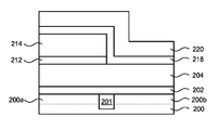
- FIG. 2A schematically shows a substrate 200 containing a PMOS device region 200 a and a NMOS device region 200 b that are separated by a shallow trench isolation (STI) 201 .
- the substrate 200 and the regions 200 a / 200 b may contain bulk silicon substrate, single crystal silicon (doped or undoped), semiconductor on insulator (SOI) substrate, or any other semiconductor material including, for example, Si, SiC, SiGe, SiGeC, Ge, GaAs, InAs, InP, as well as other III/V or II/VI compound semiconductors or any combinations thereof.
- SOI semiconductor on insulator
- the substrate 200 can be of any size, for example a 200 mm substrate, a 300 mm substrate, or an even larger substrate.
- the substrate 200 can include a tensile-strained Si layer.
- the substrate 200 may contain Ge or Si x Ge 1-x compounds, where x is the atomic fraction of Si, 1-x is the atomic fraction of Ge, and 0 ⁇ 1-x ⁇ 1.
- Exemplary Si x Ge 1-x compounds include Si 0.1 Ge 0.9 , Si 0.2 Ge 0.8 , Si 0.3 Ge 0.7 , Si 0.4 Ge 0.6 , Si 0.5 Ge 0.5 , Si 0.6 Ge 0.4 , Si 0.7 Ge 0.3 , Si 0.8 Ge 0.2 , and Si 0.9 Ge 0.1 .
- the substrate 200 can contain a compressive-strained Ge layer or a tensile-strained Si x Ge 1-x (x>0.5) deposited on a relaxed Si 0.5 Ge 0.5 buffer layer.
- the substrate 200 includes Si and the PMOS device region 200 a contains Si x Ge 1-x .
- the STI 201 is formed to electrically isolate the PMOS device region 200 a from the NMOS device region 200 b and the STI 201 horizontally defines boundaries of the device regions 200 a and 200 b .
- the STI 201 may be formed using conventional methods, for example by selectively etching an opening in the substrate 200 using a patterned mask or photoresist, depositing silicon oxide or silicon nitride to fill the opening, and then planarizing the oxide or nitride.
- the PMOS device region 200 a is doped with p-type dopants and the NMOS device region 200 b is doped with n-type dopants.
- FIG. 2A further shows an interface layer 202 is formed on the PMOS device region 200 a and the NMOS device region 200 b .
- the interface layer 202 can, for example, contain high mobility, low defect oxide (e.g., SiO 2 ).
- the interface layer 202 may be a chemical oxide formed by oxidizing a surface of substrate 200 in an aqueous bath (e.g., a bath containing deionized (DI) water and ozone (O 3 )), an oxide formed by oxidation of a surface of substrate 200 during or following the deposition of the high-k film 204 , or an oxide deposited onto a surface of substrate 200 by gas phase deposition using reactant gases.
- the interface layer 202 can have a thickness between about 6 Angstrom and about 15 Angstrom, for example.
- FIG. 2B shows a high-k film 204 deposited on the interface layer 202 .
- the interface layer 202 has a lower dielectric constant than the high-k film 204 and, therefore, the presence of the interface layer 202 increases the effective oxide thickness (EOT) of the combination of the interface layer 202 and the high-k film 204 .
- EOT effective oxide thickness
- the high-k film 204 can contain hafnium, zirconium, or hafnium and zirconium, including hafnium oxide (HfO 2 ), hafnium oxynitride (HfON), hafnium silicate (HfSiO), hafnium silicon oxynitride (HfSiON), zirconium oxide (ZrO 2 ), zirconium oxynitride (ZrON), zirconium silicate (ZrSiO), zirconium silicon oxynitride (ZrSiON), hafnium zirconium oxide (HfZrO 2 ), hafnium zirconium oxynitride (HfZrON), hafnium zirconium silicate (HfZrSiO), hafnium zirconium silicon oxynitride (HfZrSiON), or a combination of two or more thereof.
- hafnium oxide HfO 2
- the high-k film 204 can contain an oxide, oxynitride, or titanate layer containing one or more elements selected from Group II (beryllium (Be), magnesium (Mg), calcium (Ca), strontium (Sr), and barium (Ba)), and elements selected from rare earth metals of the Periodic Table of the Elements.
- Group II beryllium (Be), magnesium (Mg), calcium (Ca), strontium (Sr), and barium (Ba)
- elements selected from rare earth metals of the Periodic Table of the Elements selected from Group II (beryllium (Be), magnesium (Mg), calcium (Ca), strontium (Sr), and barium (Ba)
- Rare earth metals include yttrium (Y), lanthanum (La), cerium (Ce), praseodymium (Pr), neodymium (Nd), promethium (Pm), samarium (Sm), europium (Eu), gadolinium (Gd), terbium (Tb), dysprosium (Dy), holmium (Ho), erbium (Er), thulium (Tm), ytterbium (Yb), and lutetium (Lu).
- Examples of rare earth metal oxides include yttrium oxide (Y 2 O 3 ), lanthanium oxide (La 2 O 3 ) and lutetium oxide (Lu 2 O 3 ).
- titanate layers include barium titanate (BaTiO 3 ), strontium titanate (SrTiO 3 ), and barium strontium titanate (BaSrTiO 3 ).
- the high-k film 204 may be deposited by atomic layer deposition (ALD), plasma-enhanced ALD (PEALD), chemical vapor deposition (CVD), or plasma-enhanced CVD (PECVD).
- ALD or PEALD may be utilized due to normally superior uniformity and atomic level thickness control compared to CVD and PECVD methods.
- a thickness of the high-k film 204 can, for example, be at least 2 Angstrom, between about 2 Angstrom and about 60 Angstrom, between about 5 Angstrom and about 30 Angstrom, or between about 5 Angstrom and about 15 Angstrom.
- FIG. 2C shows a cap layer 206 deposited on the high-k film 204 over the PMOS device region 200 a and the NMOS device region 200 b .
- the cap layer 206 has a different chemical composition than the high-k film 204 .
- the cap layer 206 contains a first chemical element capable of scavenging oxygen from the interface layer 202 .
- the cap layer 206 includes a metal layer (i.e., zero valent metal) and the second chemical element is selected from Ti, Ta, Al, Ga, Mg, Ca Sr, Ba, Sc, Y, La, Ce, Pr, Nd, Pm, Sm, Eu, Gd, Tb, Dy, Ho, Er, Tm, Yb, or Lu, or a combination thereof.
- the cap layer 206 may be deposited by atomic layer deposition (ALD), plasma-enhanced ALD (PEALD), chemical vapor deposition (CVD), plasma-enhanced CVD (PECVD), or sputtering.
- a thickness of the cap layer 206 can, for example, be between about 5 Angstrom and about 200 Angstrom, between about 10 Angstrom and about 30 Angstrom, between about 30 Angstrom and about 100 Angstrom, or between about 100 Angstrom and about 200 Angstrom.
- the thickness of the cap layer 206 is selected to provide desired reduction or elimination of the interface layer 202 by scavenging of oxygen by the first chemical element in the cap layer 206 .
- the reduction or elimination of the interface layer 202 occurs by oxygen diffusion from the interface layer 202 into the cap layer 206 during a heat-treating process.
- FIG. 2C further shows an optional first barrier film 208 containing, for example, one or more of TiN, TiC, TiCN, TiAlN, TiSiN, TaN, TaC, TaCN, TaAlN, TaSiN, amorphous Si, or poly-Si, deposited on the cap layer 206 .
- a thickness of the optional first barrier film 208 can be between about 50 and 200 Angstrom, for example.
- the optional first barrier film 208 provides physical separation of the cap layer 206 from any subsequent layers formed on the optional first barrier film 208 , such as a mask layer or photoresist.
- the optional first barrier film 208 can prevent or significantly reduce oxygen diffusion into the cap layer 206 from a gaseous environment during heat-treating processes.
- FIG. 2D shows a first cap layer 212 selectively formed on the high-k film 204 in the PMOS device region 200 a and a patterned optional first barrier film 214 formed on the first cap layer 212 .
- the patterned film structure in FIG. 2D may be formed by removing the cap layer 206 and the optional first barrier film 208 in the NMOS device region 200 b by standard lithography and etching methods that can utilize a patterned mask 216 formed over the PMOS device region 200 a .
- the pattern transfer may use one or more etching steps to remove the unprotected portions of the optional first barrier film 208 and the cap layer 206 above the high-k film 204 in the NMOS device region 200 b .
- the one or more etching steps can, for example, include plasma etching, reactive ion etching (RIE), or wet etching using an etchant species in liquid solution.
- the patterned mask 216 can contain photoresist.
- the patterned mask 216 can contain an organic mask or silicon nitride (SiN).
- a photolithography tool may be used to image a pattern onto a photoresist material (not shown) deposited on the film structure in FIG. 2C .
- the patterned mask 216 provides a physical barrier during a subsequent etching process that selectively removes material not protected by the patterned mask 216 .
- the patterned optional first barrier film 214 e.g., TiN
- the cap layer 206 may be plasma etched with high etch selectivity to the high-k film 204 using a chlorine-based process gas (e.g., BCl 3 /Cl 2 /O 2 /Ar).
- a chlorine-based process gas e.g., BCl 3 /Cl 2 /O 2 /Ar
- low substrate temperatures e.g., less than 200° C., for example around room temperature and below
- a fluorine-based process gas e.g., CF 4 /O 2
- CF 4 /O 2 may be used at temperatures above room temperature while maintaining high etch selectivity to the high-k film 204 .
- the patterned mask 216 is removed, for example, using a non-oxidizing ashing process or a wet etching process that avoids oxidizing the patterned optional first barrier film 214 and the first cap layer 212 .
- an organic mask may be removed in a plasma process using a process gas containing N 2 /H 2 .
- the patterned optional first barrier film 214 e.g., TiN
- the patterned mask 216 may be selectively removed relative to the high-k film 204 using a wet etching process utilizing a combination of NH 4 OH and HF.
- FIG. 2E schematically shows a second cap layer 218 deposited over the first cap layer 212 and on the high-k film 204 in the exposed NMOS device region 200 b .
- the second cap layer 218 contains a second chemical element for diffusion into the high-k film 204 in the NMOS device region 200 b during a heat-treating process.
- the second cap layer 206 has a different chemical composition than the high-k film 204 and the first cap layer 212 and includes a dielectric material containing a first chemical element selected from Mg, Ca, Sr, Ba, Sc, Y, La, Ce, Pr, Nd, Pm, Sm, Eu, Gd, Tb, Dy, Ho, Er, Tm, Yb, or Lu, or a combination thereof.
- the dielectric material can contain a metal oxide, a metal nitride, or a metal oxynitride, or a combination thereof.
- rare earth metal oxides include yttrium oxide (Y 2 O 3 ), lanthanium oxide (La 2 O 3 ) and lutetium oxide (Lu 2 O 3 ).
- the second cap layer 218 may be deposited by atomic layer deposition (ALD), plasma-enhanced ALD (PEALD), chemical vapor deposition (CVD), plasma-enhanced CVD (PECVD), or sputtering.
- a thickness of the second cap layer 218 can, for example, be between about 5 Angstrom and about 200 Angstrom, between about 10 Angstrom and about 30 Angstrom, between about 30 Angstrom and about 200 Angstrom, or between about 200 Angstrom and about 200 Angstrom.
- the thickness of the second cap layer 206 is selected to provide an adequate supply of the second chemical element for diffusion into the high-k film 204 in the NMOS device region 200 b to reach a targeted threshold voltage shift. In other words, the thicker the second cap layer 218 , the greater the available supply of the second chemical element.
- FIG. 2E further shows an optional second barrier film 220 containing, for example, one or more layers of TiN, TiC, TiCN, TiAlN, TiSiN, TaN, TaC, TaCN, TaAlN, TaSiN, amorphous Si, or poly-Si, deposited on the second cap layer 218 .
- a thickness of the optional second barrier film 220 can be between about 50 Angstrom and 200 Angstrom, for example.
- the optional second barrier film 220 provides physical separation of the second cap layer 218 from any further layers formed on the optional second barrier film 220 .
- the optional second barrier film 220 can prevent or reduce oxygen diffusion into the second cap layer 218 from a gaseous environment during heat-treating processes.
- FIG. 2F schematically shows a heat-treating process performed to diffuse the second chemical element 218 a from the second cap layer 218 into the high-k film 204 in the NMOS device region 200 b .
- first chemical element 212 a e.g., Al
- first chemical element 212 a may diffuse from the first cap layer 212 into the high-k film 204 in the PMOS device region 200 a .
- oxygen species 202 a diffuse from the interface layer 202 (e.g., SiO 2 ) through the high-k film 204 and the first cap layer 212 in the PMOS device region 200 a , and into the second cap layer 218 over the PMOS and NMOS device regions 200 a / 200 b , thereby reducing the thickness of or eliminating the interface layer 202 .
- the interface layer 202 e.g., SiO 2
- the heat-treating process may utilize a substrate temperature, time, and gaseous environment (e.g., an inert gaseous environment containing a noble gas or N 2 ), that results in a targeted diffusion of the second chemical element 218 a (e.g., La or Ba) into the high-k film 204 in the NMOS device region 200 b , and optionally diffusion of the first chemical element 212 a (e.g., Al) into the high-k film 204 in the PMOS device region 200 a .
- the heat-treating may include a rapid thermal anneal (RTA) with a fast positive temperature ramping rate to a target temperature between about 800° C.
- RTA rapid thermal anneal
- target temperatures may be used, for example between about 900° C. and 1100° C., or between 1000° C. and 1200° C.
- the second cap layer 218 scavenges oxygen from the interface layer 202 by oxygen diffusion through the high-k film 204 and the first cap layer 212 , and into the second cap layer 218 in both the PMOS device region 200 a and the NMOS device region 200 b . Further, the second cap layer 218 may scavenge oxygen diffusing through other material layers from a gaseous processing environment during the heat-treating. This oxygen scavenging maintains a constant or nearly constant device threshold voltage, even after a high temperature heat-treating or anneal in an oxygen ambient. By reducing the thickness of or eliminating the interface layer 202 altogether, the effective oxide thickness (EOT) of the composite gate stack is reduced, thereby, enhancing the scalability of the composite gate stack and performance of the field effect transistor.
- EOT effective oxide thickness
- FIG. 2G schematically shows the resulting film structure following the heat-treating process.
- the diffusion described above forms a first high-k film 222 over the PMOS device region 200 a and a second high-k film 224 over the NMOS device region 200 b .
- the interface layer 202 from FIG. 2E is reduced in thickness or eliminated by the scavenging properties of the second cap layer 218 .
- further processing includes removing from the high-k film 204 the first cap layer 212 , the second cap layer 218 , the patterned optional first barrier film 214 , and the optional second barrier film 220 .
- Those films and layers may be removed using a plasma formed from a chlorine-based process gas (e.g., BCl 3 /Cl 2 /O 2 /Ar) with high etch selectivity to the first high-k film 222 and the second high-k film 224 .
- a chlorine-based process gas e.g., BCl 3 /Cl 2 /O 2 /Ar
- low substrate temperatures e.g., approximately room temperature and below
- the high etch selectivity may be lost at temperatures above 200° C. due to increased volatility of the etch products at these temperatures.
- a fluorine-based process gas e.g., CF 4 /O 2
- CF 4 /O 2 fluorine-based process gas
- fluorine chemistry is normally not effective in etching aluminum in the second cap layer 218 .
- a wet etching process that uses a combination of phosphoric acid, acetic acid, and nitric acid may be used to remove TiN, Al and oxidized Al metal, with good selectivity to the first high-k film 222 and the second high-k film 224 .
- a gate electrode film 230 is deposited on the first high-k film 222 and the second high-k film 224 .
- the gate electrode film 230 can, for example, have a thickness between about 5 nm (nanometers) and about 40 nm, or between about 5 nm and about 10 nm and can, for example, contain W, WN, WSi x , Al, Mo, Ta, TaN, TaSiN, HfN, HfSiN, Ti, TiN, TiSiN, Mo, MoN, Re, Pt, Ru, or Si.
- FIG. 2H shows the film stack following deposition of the gate electrode film 230 on first high-k film 222 and the second high-k film 224 .
- embodiments of the invention enable the use of the same gate electrode film 230 in both the PMOS device region 200 a the NMOS device region 200 b .
- This provides a gate stack with the same stack height for both the PMOS device region 200 a and the NMOS device region 200 b which can simplify processing of the gate stack in subsequent etching steps compared to a dual-metal-containing gate integration where two different gate stack heights must be simultaneously etched.
- well-known processing schemes may be utilized.
- a gate first integration can continue as normal.
- a gate last integration is similarly possible by using a Si gate electrode 230 instead of a TiN gate electrode 230 .
- FIGS. 2A-2H illustrate an embodiment of the invention that includes providing a substrate with defined NMOS and PMOS device regions, and an interface layer on the NMOS and PMOS device regions, depositing a high-k film on the interface layer, and depositing a first cap layer on the high-k film, wherein the first cap layer contains a first chemical element for scavenging oxygen from the interface layer.
- the method further includes removing the first cap layer from the high-k film in the NMOS device region, depositing a second cap layer on the first cap layer in the PMOS device region and on the high-k film in the NMOS device region, where the second cap layer contains a second chemical element for modifying the high-k film in the NMOS device region.
- the method still further includes performing a heat-treating process to diffuse the second chemical element into the high-k film in the NMOS device region and to reduce or eliminate the interface layer by oxygen diffusion from the interface layer through the high-k film into the second cap layer, removing the first and second cap layers from the high-k film, and depositing a gate electrode film over the high-k film.
- FIG. 3A illustrates a processing system 1 that may be utilized for depositing one or more of the films and layers described above, including the high-k film 104 , the cap layer 106 , and the second cap layer 118 according to one embodiment of the invention.
- the processing system 1 may be configured for performing ALD or CVD processing.
- the processing system 1 includes a process chamber 10 having a substrate holder 20 configured to support a substrate 100 , upon which the film or layer is formed.
- the process chamber 10 further contains an upper assembly 30 (e.g., a showerhead) coupled to a first precursor supply system 40 (e.g., hafnium precursor supply system), a second precursor supply system 42 (e.g., lanthanum or aluminum precursor supply system), a purge gas supply system 44 , an oxygen-containing gas supply system 46 , a nitrogen-containing gas supply system 48 , and an auxiliary gas supply system 50 for supplying one or more elements selected from Mg, Ca, Sr, Ba Sc, Y, La, Ce, Pr, Nd, Pm, Sm, Eu, Gd, Tb, Dy, Ho, Er, Tm, Yb, or Lu, or a combination thereof, or other elements, for example silicon.
- a first precursor supply system 40 e.g., hafnium precursor supply system
- a second precursor supply system 42 e.g., lanthanum or aluminum precursor supply system
- a purge gas supply system 44 supplying one or more elements selected from Mg, Ca, Sr,
- processing system 1 includes a substrate temperature control system 60 coupled to substrate holder 20 and configured to elevate and control the temperature of substrate 100 .
- processing system 1 includes a controller 70 that can be coupled to process chamber 10 , substrate holder 20 , upper assembly 30 configured for introducing process gases into the process chamber 10 , first precursor supply system 40 , second precursor supply system 42 , purge gas supply system 44 , oxygen-containing gas supply system 46 , nitrogen-containing gas supply system 48 , auxiliary gas supply system 50 , and substrate temperature control system 60 .
- controller 70 can be coupled to one or more additional controllers/computers (not shown), and controller 70 can obtain setup and/or configuration information from an additional controller/computer.
- the processing system 1 can include any number of processing elements having any number of controllers associated with them in addition to independent processing elements.
- the controller 70 can be used to configure any number of processing elements ( 10 , 20 , 30 , 40 , 42 , 44 , 46 , 48 , 50 , and 60 ), and the controller 70 can collect, provide, process, store, and display data from processing elements.
- the controller 70 can comprise a number of applications for controlling one or more of the processing elements.
- controller 70 can include a graphic user interface (GUI) component (not shown) that can provide easy to use interfaces that enable a user to monitor and/or control one or more processing elements.
- GUI graphic user interface
- the first precursor supply system 40 and the second precursor supply system 42 may be configured to alternately or simultaneously introduce a first precursor and a second precursor to process chamber 10 .
- the alternation of the introduction of the first and second precursors can be cyclical, or it may be acyclical with variable time periods between introduction of the first and second precursors.
- first and/or second precursors may be utilized for introducing the first and/or second precursors to the process chamber 10 .
- One method includes vaporizing precursors through the use of separate bubblers or direct liquid injection (DLI) systems, or a combination thereof, and then mixing in the gas phase within or prior to introduction into the process chamber 10 .
- DLI systems have been shown to reduce premature thermal decomposition of precursors over bubbling methods.
- Another method of delivering the first and second precursors includes separately controlling two or more different liquid sources (neat precursors or precursor solutions), which are then mixed prior to entering a common vaporizer.
- hafnium zirconium based films can contain between 5 and 95 atomic percent zirconium (5% ⁇ % Zr/(% Zr+% Hf) ⁇ 95%), and between 5 and 95 atomic percent hafnium (5% ⁇ % Hf/(% Zr+% Hf) ⁇ 95%).
- Embodiments of the invention may utilize a wide variety of hafnium and zirconium precursors.
- representative examples include: Hf(O t Bu) 4 (hafnium tert-butoxide, HTB), Hf(NEt 2 ) 4 (tetrakis(diethylamido)hafnium, TDEAH), Hf(NEtMe) 4 (tetrakis(ethylmethylamido)hafnium, TEMAH), Hf(NMe 2 ) 4 (tetrakis(dimethylamido)hafnium, TDMAH), Zr(O t Bu) 4 (zirconium tert-butoxide, ZTB), Zr(NEt 2 ) 4 (tetrakis(diethylamido)zirconium, TDEAZ), Zr(NMeEt) 4 (tetrakis(ethylmethylamido)zirconium, TEMAZ), Zr(NMe 2 )
- Embodiments of the invention may utilize one or more of a wide variety of different elements selected from Group II, Group III, Group XIII, and rare earth metals of the Periodic Table.
- the elements may be provided using any precursor gases that have sufficient reactivity, thermal stability, and volatility.
- the precursor gases may be delivered to the process chamber using bubbling or DLI methods described above for hafnium and zirconium precursors.
- Embodiments of the inventions may utilize a wide variety of different rare earth precursors.
- many rare earth precursors have the formula: ML 1 L 2 L 3 D x where M is a rare earth metal element selected from the group of yttrium (Y), lutetium (Lu), lanthanum (La), cerium (Ce), praseodymium (Pr), neodymium (Nd), samarium (Sm), europium (Eu), gadolinium (Gd), terbium (Tb), dysprosium (Dy), holmium (Ho), erbium (Er), thulium (Tm), and ytterbium (Yb).
- Y yttrium
- Lu lutetium
- La lanthanum
- Ce cerium
- Pr praseodymium
- Nd neodymium
- Sm samarium
- Eu europium
- Gd gadolinium
- Tb ter
- L 1 , L 2 , L 3 are individual anionic ligands
- D is a neutral donor ligand where x can be 0, 1, 2, or 3.
- Each L 1 , L 2 , L 3 ligand may be individually selected from the groups of alkoxides, halides, aryloxides, amides, cyclopentadienyls, alkyls, silyls, amidinates, ⁇ -diketonates, ketoiminates, silanoates, and carboxylates.
- D ligands may be selected from groups of ethers, furans, pyridines, pyroles, pyrrolidines, amines, crown ethers, glymes, and nitriles.
- L group alkoxides include tert-butoxide, iso-propoxide, ethoxide, 1-methoxy-2,2-dimethyl-2-propionate (mmp), 1-dimethylamino-2,2′-dimethyl-propionate, amyloxide, and neo-pentoxide.
- halides include fluoride, chloride, iodide, and bromide.
- aryloxides include phenoxide and 2,4,6-trimethylphenoxide.
- amides include bis(trimethylsilyl)amide di-tert-butylamide, and 2,2,6,6-tetramethylpiperidide (TMPD).
- cyclopentadienyls include cyclopentadienyl, 1-methylcyclopentadienyl, 1,2,3,4-tetramethylcyclopentadienyl, 1-ethylcyclopentadienyl, pentamethylcyclopentadienyl, 1-iso-propylcyclopentadienyl, 1-n-propylcyclopentadienyl, and 1-n-butylcyclopentadienyl.
- alkyls include bis(trimethylsilyl)methyl, tris(trimethylsilyl)methyl, and trimethylsilylmethyl.
- An example of a silyl is trimethylsilyl.
- amidinates include N,N′-di-tert-butylacetamidinate, N,N′-di-iso-propylacetamidinate, N,N′-di-isopropyl-2-tert-butylamidinate, and N,N′-di-tert-butyl-2-tert-butylamidinate.
- ⁇ -diketonates include 2,2,6,6-tetramethyl-3,5-heptanedionate (THD), hexafluoro-2,4-pentandionate, and 6,6,7,7,8,8,8-heptafluoro-2,2-dimethyl-3,5-octanedionate (FOD).
- ketoiminate 2-iso-propylimino-4-pentanonate.
- silanoates include tri-tert-butylsiloxide and triethylsiloxide.
- An example of a carboxylate is 2-ethylhexanoate.
- D ligands examples include tetrahydrofuran, diethylether, 1,2-dimethoxyethane, diglyme, triglyme, tetraglyme, 12-Crown-6,10-Crown-4, pyridine, N-methylpyrrolidine, triethylamine, trimethylamine, acetonitrile, and 2,2-dimethylpropionitrile.
- rare earth precursors include: Y precursors: Y(N(SiMe 3 ) 2 ) 3 , Y(N(iPr) 2 ) 3 , Y(N(tBu)SiMe 3 ) 3 , Y(TMPD) 3 , Cp 3 Y, (MeCp) 3 Y, ((nPr)Cp) 3 Y, ((nBu)Cp) 3 Y, Y(OCMe 2 CH 2 NMe 2 ) 3 , Y(THD) 3 , Y[OOCCH(C 2 H 5 )C 4 H 9 ] 3 , Y(C 11 H 19 O 2 ) 3 CH 3 (OCH 2 CH 2 ) 3 OCH 3 , Y(CF 3 COCHCOCF 3 ) 3 , Y(OOCC 10 H 7 ) 3 , Y(OOC 10 H 19 ) 3 , and Y(O(iPr)) 3 .
- La precursors La(N(SiMe 3 ) 2 ) 3 , La(N(iPr) 2 ) 3 , La(N(tBu)SiMe 3 ) 3 , La(TMPD) 3 , ((iPr)Cp) 3 La, Cp 3 La, Cp 3 La(NCCH 3 ) 2 , La(Me 2 NC 2 H 4 Cp) 3 , La(THD) 3 , La[OOCCH(C 2 H 5 )C 4 H 9 ] 3 , La(C 11 H 19 O 2 ) 3 .CH 3 (OCH 2 CH 2 ) 3 OCH 3 , La(C 11 H 19 O 2 ) 3 .CH 3 (OCH 2 CH 2 ) 4 OCH 3 , La(O(iPr)) 3 , La(OEt) 3 , La(acac) 3 , La(((tBu) 2 N) 2 CMe) 3 , La((iPr) 2 N) 2 CMe) 3
- Ce precursors Ce(N(SiMe 3 ) 2 ) 3 , Ce(N(iPr) 2 ) 3 , Ce(N(tBu)SiMe 3 ) 3 , Ce(TMPD) 3 , Ce(FOD) 3 , ((iPr)Cp) 3 Ce, Cp 3 Ce, Ce(Me 4 Cp) 3 , Ce(OCMe 2 CH 2 NMe 2 ) 3 , Ce(THD) 3 , Ce[OOCCH(C 2 H 5 )C 4 H 9 ] 3 , Ce(C 11 H 19 O 2 ) 3 .CH 3 (OCH 2 CH 2 ) 3 OCH 3 , Ce(C 11 H 19 O 2 ) 3 .CH 3 (OCH 2 CH 2 ) 4 OCH 3 , Ce(O(iPr)) 3 , and Ce(acac) 3 .
- Pr precursors Pr(N(SiMe 3 ) 2 ) 3 , ((iPr)Cp) 3 Pr, Cp 3 Pr, Pr(THD) 3 , Pr(FOD) 3 , (C 5 Me 4 H) 3 Pr, Pr[OOCCH(C 2 H 5 )C 4 H 9 ] 3 , Pr(C 11 H 19 O 2 ) 3 .CH 3 (OCH 2 CH 2 ) 3 OCH 3 , Pr(O(iPr)) 3 , Pr(acac) 3 , Pr(hfac) 3 , Pr(((tBu) 2 N) 2 CMe) 3 , Pr(((iPr) 2 N) 2 CMe) 3 , Pr(((tBu) 2 N) 2 C(tBu)) 3 , and Pr(((iPr) 2 N) 2 C(tBu)) 3 .
- Nd precursors Nd(N(SiMe 3 ) 2 ) 3 , Nd(N(iPr) 2 ) 3 , ((iPr)Cp) 3 Nd, Cp 3 Nd, (C 5 Me 4 H) 3 Nd, Nd(THD) 3 , Nd[OOCCH(C 2 H 5 )C 4 H 9 ] 3 , Nd(O(iPr)) 3 , Nd(acac) 3 , Nd(hfac) 3 , Nd(F 3 CC(O)CHC(O)CH 3 ) 3 , and Nd(FOD) 3 .
- Sm precursors Sm(N(SiMe 3 ) 2 ) 3 , ((iPr)Cp) 3 Sm, Cp 3 Sm, Sm(THD) 3 , Sm[OOCCH(C 2 H 5 )C 4 H 9 ] 3 , Sm(O(iPr)) 3 , Sm(acac) 3 , and (C 5 Me 5 ) 2 Sm.
- Eu precursors Eu(N(SiMe 3 ) 2 ) 3 , ((iPr)Cp) 3 Eu, Cp 3 Eu, (Me 4 Cp) 3 Eu, Eu(THD) 3 , Eu[OOCCH(C 2 H 5 )C 4 H 9 ] 3 , Eu(O(iPr)) 3 , Eu(acac) 3 , and (C 5 Me 5 ) 2 Eu.
- Tb precursors Tb(N(SiMe 3 ) 2 ) 3 , ((iPr)Cp) 3 Tb, Cp 3 Tb, Tb(THD) 3 , Tb[OOCCH(C 2 H 5 )C 4 H 9 ] 3 , Tb(O(iPr)) 3 , and Tb(acac) 3 .
- Dy precursors Dy(N(SiMe 3 ) 2 ) 3 , ((iPr)Cp) 3 Dy, Cp 3 Dy, Dy(THD) 3 , Dy[OOCCH(C 2 H 5 )C 4 H 9 ] 3 , Dy(O(iPr)) 3 , Dy(O 2 C(CH 2 ) 6 CH 3 ) 3 , and Dy(acac) 3 .
- Ho precursors Ho(N(SiMe 3 ) 2 ) 3 , ((iPr)Cp) 3 Ho, Cp 3 Ho, Ho(THD) 3 , Ho[OOCCH(C 2 H 5 )C 4 H 9 ] 3 , Ho(O(iPr)) 3 , and Ho(acac) 3 .
- Tm precursors Tm(N(SiMe 3 ) 2 ) 3 , ((iPr)Cp) 3 Tm, Cp 3 Tm, Tm(THD) 3 , Tm[OOCCH(C 2 H 5 )C 4 H 9 ] 3 , Tm(O(iPr)) 3 , and Tm(acac) 3 .
- Lu precursors Lu(N(SiMe 3 ) 2 ) 3 , ((iPr)Cp) 3 Lu, Cp 3 Lu, Lu(THD) 3 , Lu[OOCCH(C 2 H 5 )C 4 H 9 ] 3 , Lu(O(iPr)) 3 , and Lu(acac) 3 .
- Si silicon; Me: methyl; Et: ethyl; iPr: isopropyl; nPr: n-propyl; Bu: butyl; nBu: n-butyl; sBu: sec-butyl; iBu: iso-butyl; tBu: tert-butyl; Cp: cyclopentadienyl; THD: 2,2,6,6-tetramethyl-3,5-heptanedionate; TMPD: 2,2,6,6-tetramethylpiperidide; acac: acetylacetonate; hfac: hexafluoroacetylacetonate; and FOD: 6,6,7,7,8,8,8-heptafluoro-2,2-dimethyl-3,5-octanedionate.
- Common C 1 and C 2 alkylhydrazine compounds include monomethyl-hydrazine (MeNHNH 2 ), 1,1-dimethyl-hydrazine (Me 2 NNH 2 ), and 1,2-dimethyl-hydrazine (MeNHNHMe).
- an oxygen- and nitrogen-containing gas may be utilized, for example, NO, NO 2 , or N 2 O, or a combination thereof, and optionally an inert gas such as Ar.
- Embodiments of the inventions may utilize a wide variety of different Group II (alkaline earth) precursors.
- Group II precursors have the formula: ML 1 L 2 D x where M is an alkaline earth metal element selected from the group of beryllium (Be), magnesium (Mg), calcium (Ca), strontium (Sr), and barium (Ba).
- L 1 and L 2 are individual anionic ligands, and D is a neutral donor ligand where x can be 0, 1, 2, or 3.
- Each L 1 , L 2 ligand may be individually selected from the groups of alkoxides, halides, aryloxides, amides, cyclopentadienyls, alkyls, silyls, amidinates, ⁇ -diketonates, ketoiminates, silanoates, and carboxylates.
- D ligands may be selected from groups of ethers, furans, pyridines, pyroles, pyrrolidines, amines, crown ethers, glymes, and nitriles.
- L group alkoxides include tert-butoxide, iso-propoxide, ethoxide, 1-methoxy-2,2-dimethyl-2-propionate (mmp), 1-dimethylamino-2,2′-dimethyl-propionate, amyloxide, and neo-pentoxide.
- halides include fluoride, chloride, iodide, and bromide.
- aryloxides include phenoxide and 2,4,6-trimethylphenoxide.
- amides include bis(trimethylsilyl)amide di-tert-butylamide, and 2,2,6,6-tetramethylpiperidide (TMPD).
- cyclepentadienyls include cyclopentadienyl, 1-methylcyclopentadienyl, 1,2,3,4-tetramethylcyclopentadienyl, 1-ethylcyclopentadienyl, pentamethylcyclopentadienyl, 1-iso-propylcyclopentadienyl, 1-n-propylcyclopentadienyl, and 1-n-butylcyclopentadienyl.
- alkyls include bis(trimethylsilyl)methyl, tris(trimethylsilyl)methyl, and trimethylsilylmethyl.
- An example of a silyl is trimethylsilyl.
- amidinates include N,N′-di-tert-butylacetamidinate, N,N′-di-iso-propylacetamidinate, N,N′-di-isopropyl-2-tert-butylamidinate, and N,N′-di-tert-butyl-2-tert-butylamidinate.
- ⁇ -diketonates include 2,2,6,6-tetramethyl-3,5-heptanedionate (THD), hexafluoro-2,4-pentanedionate (hfac), and 6,6,7,7,8,8,8-heptafluoro-2,2-dimethyl-3,5-octanedionate (FOD).
- ketoiminate 2-iso-propylimino-4-pentanonate.
- silanoates include tri-tert-butylsiloxide and triethylsiloxide.
- An example of a carboxylate is 2-ethylhexanoate.
- D ligands examples include tetrahydrofuran, diethylether, 1,2-dimethoxyethane, diglyme, triglyme, tetraglyme, 12-Crown-6,10-Crown-4, pyridine, N-methylpyrrolidine, triethylamine, trimethylamine, acetonitrile, and 2,2-dimethylpropionitrile.
- Group II (alkaline earth) precursors include:
- Be precursors Be(N(SiMe 3 ) 2 ) 2 , Be(TMPD) 2 , and BeEt 2 .
- Ca precursors Ca(N(SiMe 3 ) 2 ) 2 , Ca(iPr 4 Cp) 2 , and Ca(Me 5 Cp) 2 .
- Sr precursors Bis(tert-butylacetamidinato)strontium (TBAASr), Sr(N(SiMe 3 ) 2 ) 2 , Sr(THD) 2 , Sr(THD) 2 (tetraglyme), Sr(iPr 4 Cp) 2 , Sr(iPr 3 Cp) 2 , and Sr(Me 5 Cp) 2 .
- Ba precursors Bis(tert-butylacetamidinato)barium (TBAABa), Ba(N(SiMe 3 ) 2 ) 2 , Ba(THD) 2 , Ba(THD) 2 (tetraglyme), Ba(iPr 4 Cp) 2 , Ba(Me 5 Cp) 2 , and Ba(nPrMe 4 Cp) 2 .
- Embodiments of the inventions may utilize a wide variety of different precursors for Group XIII high-k forming elements (B, Al, Ga, In, Tl) into the hafnium zirconium based films.
- Group XIII high-k forming elements B, Al, Ga, In, Tl
- many Al precursors have the formula: AlL 1 L 2 L 3 D x where L 1 , L 2 , L 3 are individual anionic ligands, and D is a neutral donor ligand where x can be 0, 1, or 2.
- Each L 1 , L 2 , L 3 ligand may be individually selected from the groups of alkoxides, halides, aryloxides, amides, cyclopentadienyls, alkyls, silyls, amidinates, ⁇ -diketonates, ketoiminates, silanoates, and carboxylates.
- D ligands may be selected from groups of ethers, furans, pyridines, pyroles, pyrrolidines, amines, crown ethers, glymes, and nitriles.
- Al precursors include: Al 2 Me 6 , Al 2 Et 6 , [Al(O(sBu)) 3 ] 4 , Al(CH 3 COCHCOCH 3 ) 3 , AlBr 3 , AlI 3 , Al(O(iPr)) 3 , [Al(NMe 2 ) 3 ] 2 , Al(iBU) 2 Cl 5 Al(iBu) 3 , Al(iBu) 2 H, AlEt 2 Cl, Et 3 Al 2 (O(sBu)) 3 , and Al(THD) 3 .
- Ga precursors include GaCl 3 and GaH 3
- examples of 1n precursors include InCl 3 and InH 3
- examples of B precursors include borane (BH 3 ), diborane (B 2 H 6 ), tri-ethylboron (BEt 3 ), triphenylboron (BPh 3 ), and borane adducts such as Me 3 N:BH 3 , and BCl 3 .
- Embodiments of the invention may utilize a wide variety of silicon precursors for incorporating silicon into the films or layers.
- silicon precursors include, but are not limited to, silane (SiH 4 ), disilane (Si 2 H 6 ), monochlorosilane (SiClH 3 ), dichlorosilane (SiH 2 Cl 2 ), trichlorosilane (SiHCl 3 ), hexachlorodisilane (Si 2 Cl 6 ), diethylsilane (Et 2 SiH 2 ), and alkylaminosilane compounds.
- alkylaminosilane compounds include, but are not limited to, di-isopropylaminosilane (H 3 Si(NPr 2 )), bis(tert-butylamino)silane ((C 4 H 9 (H)N) 2 SiH 2 ), tetrakis(dimethylamino)silane (Si(NMe 2 ) 4 ), tetrakis(ethylmethylamino)silane (Si(NEtMe) 4 ), tetrakis(diethylamino)silane (Si(NEt 2 ) 4 ), tris(dimethylamino)silane (HSi(NMe 2 ) 3 ), tris(ethylmethylamino)silane (HSi(NEtMe) 3 ), tris(diethylamino)silane (HSi(NEt 2 ) 3 ), and tris(dimethylhydrazino)silane (HSi(
- the purge gas supply system 44 is configured to introduce a purge gas to process chamber 10 .
- the introduction of purge gas may occur between introduction of pulses of first and second precursors and an oxygen-containing gas, a nitrogen-containing gas, an oxygen- and a nitrogen-containing gas, or a high-k forming gas to the process chamber 10 .
- the purge gas can contain an inert gas, such as a noble gas (i.e., He, Ne, Ar, Kr, Xe), nitrogen (N 2 ), or hydrogen (H 2 ).
- the substrate temperature can, for example, range from approximately 150° C. to 350° C. It is to be understood, however, that the temperature of the substrate is selected based on the desired temperature for causing deposition of a particular dielectric material on the surface of a given substrate.
- substrate holder 20 can include a mechanical clamping system, or an electrical clamping system, such as an electrostatic clamping system, to affix substrate 100 to an upper surface of substrate holder 20 .
- substrate holder 20 can further include a substrate backside gas delivery system configured to introduce gas to the back-side of substrate 100 in order to improve the gas-gap thermal conductance between substrate 100 and substrate holder 20 .
- a substrate backside gas delivery system configured to introduce gas to the back-side of substrate 100 in order to improve the gas-gap thermal conductance between substrate 100 and substrate holder 20 .
- the substrate backside gas system can contain a two-zone gas distribution system, wherein the helium gas gap pressure can be independently varied between the center and the edge of substrate 100 .
- the process chamber 10 is further coupled to a pressure control system 32 , including a vacuum pumping system 34 and a valve 36 , through a duct 38 , wherein the pressure control system 32 is configured to controllably evacuate the process chamber 10 to a pressure suitable for forming the thin film on substrate 100 , and suitable for use of the first and second process materials.
- the vacuum pumping system 34 can include a turbo-molecular vacuum pump (TMP) or a cryogenic pump capable of a pumping speed up to about 5000 liters per second (and greater) and valve 36 can include a gate valve for throttling the chamber pressure.
- a device for monitoring chamber pressure (not shown) can be coupled to the process chamber 10 .
- the pressure control system 32 can, for example, be configured to control the process chamber pressure between about 0.1 Torr and about 100 Torr during deposition of the high-k materials.
- the first precursor supply system 40 , second precursor supply system 42 , purge gas supply system 44 , oxygen-containing gas supply system 46 , the nitrogen-containing gas supply system 48 , and auxiliary gas supply system 50 can include one or more pressure control devices, one or more flow control devices, one or more filters, one or more valves, and/or one or more flow sensors.
- the flow control devices can include pneumatic driven valves, electro-mechanical (solenoidal) valves, and/or high-rate pulsed gas injection valves.
- gases may be sequentially and alternately pulsed into the process chamber 10 , where the length of each gas pulse can, for example, be between about 0.1 sec and about 100 sec. Alternately, the length of each gas pulse can be between about 1 sec and about 10 sec.
- Exemplary gas pulse lengths for precursor gases can be between 0.3 and 3 sec, for example 1 sec.
- Exemplary gas pulse lengths for an oxygen-containing gas, a nitrogen-containing gas, and an oxygen- and nitrogen-containing gas can be between 0.3 and 3 sec, for example 1 sec.
- Exemplary purge gas pulses can be between 1 and 20 sec, for example 3 sec.
- controller 70 can contain a microprocessor, memory, and a digital I/O port capable of generating control voltages sufficient to communicate and activate inputs to the processing system 1 as well as monitor outputs from the processing system 1 .
- the controller 70 may be coupled to and may exchange information with the process chamber 10 , substrate holder 20 , upper assembly 30 , first precursor supply system 40 , second precursor supply system 42 , purge gas supply system 44 , oxygen-containing gas supply system 46 , nitrogen-containing gas supply system 48 , auxiliary gas supply system 50 , substrate temperature control system 60 , substrate temperature control system 60 , and pressure control system 32 .
- a program stored in the memory may be utilized to activate the inputs to the aforementioned components of the processing system 1 according to a process recipe in order to perform a deposition process.
- controller 70 may be implemented as a general purpose computer system that performs a portion or all of the microprocessor based processing steps of the invention in response to a processor executing one or more sequences of one or more instructions contained in a memory. Such instructions may be read into the controller memory from another computer readable medium, such as a hard disk or a removable media drive.
- processors in a multi-processing arrangement may also be employed as the controller microprocessor to execute the sequences of instructions contained in main memory.
- hard-wired circuitry may be used in place of or in combination with software instructions. Thus, embodiments are not limited to any specific combination of hardware circuitry and software.
- the controller 70 includes at least one computer readable medium or memory, such as the controller memory, for holding instructions programmed according to the teachings of the invention and for containing data structures, tables, records, or other data that may be necessary to implement the present invention.
- Examples of computer readable media are compact discs, hard disks, floppy disks, tape, magneto-optical disks, PROMs (EPROM, EEPROM, flash EPROM), DRAM, SRAM, SDRAM, or any other magnetic medium, compact discs (e.g., CD-ROM), or any other optical medium, punch cards, paper tape, or other physical medium with patterns of holes, a carrier wave (described below), or any other medium from which a computer can read.
- Such software Stored on any one or on a combination of computer readable media, resides software for controlling the controller 70 , for driving a device or devices for implementing the invention, and/or for enabling the controller to interact with a human user.
- Such software may include, but is not limited to, device drivers, operating systems, development tools, and applications software.
- Such computer readable media further includes the computer program product of the present invention for performing all or a portion (if processing is distributed) of the processing performed in implementing embodiments of the invention.
- the computer code devices may be any interpretable or executable code mechanism, including but not limited to scripts, interpretable programs, dynamic link libraries (DLLs), Java classes, and complete executable programs. Moreover, parts of the processing of the present invention may be distributed for better performance, reliability, and/or cost.
- Non-volatile media includes, for example, optical, magnetic disks, and magneto-optical disks, such as the hard disk or the removable media drive.
- Volatile media includes dynamic memory, such as the main memory.
- various forms of computer readable media may be involved in carrying out one or more sequences of one or more instructions to processor of controller for execution.
- the instructions may initially be carried on a magnetic disk of a remote computer.
- the remote computer can load the instructions for implementing all or a portion of the present invention remotely into a dynamic memory and send the instructions over a network to the controller 70 .
- the controller 70 may be locally located relative to the processing system 1 , or it may be remotely located relative to the processing system 1 .
- the controller 70 may exchange data with the processing system 1 using at least one of a direct connection, an intranet, the Internet and a wireless connection.
- the controller 70 may be coupled to an intranet at, for example, a customer site (i.e., a device maker, etc.), or it may be coupled to an intranet at, for example, a vendor site (i.e., an equipment manufacturer). Additionally, for example, the controller 70 may be coupled to the Internet.
- another computer i.e., controller, server, etc.
- the controller 70 may access, for example, the controller 70 to exchange data via at least one of a direct connection, an intranet, and the Internet.
- the controller 70 may exchange data with the processing system 1 via a wireless connection.
- FIG. 3B illustrates a plasma processing system 2 that may be utilized for depositing one or more of the films and layers described above, including the high-k film 104 , the cap layer 106 , and the second cap layer 118 according to one embodiment of the invention.
- the plasma processing system 2 may be configured for performing PEALD or PECVD processing, in addition being able to perform ALD or CVD processing.
- the plasma processing system 2 is similar to the processing system 1 described in FIG. 3A , but further includes a plasma generation system configured to generate a plasma during at least a portion of the gas exposures in the process chamber 10 . This allows formation of ozone and plasma excited oxygen from an oxygen-containing gas containing O 2 , H 2 O, H 2 O 2 , or a combination thereof.
- plasma excited nitrogen may be formed from a nitrogen-containing gas containing N 2 , NH 3 , or N 2 H 4 , or C 1 -C 10 alkylhydrazine compounds, or a combination thereof.
- plasma excited oxygen and nitrogen may be formed from a process gas containing NO, NO 2 , and N 2 O, or a combination thereof.
- the plasma generation system includes a first power source 52 coupled to the process chamber 10 , and configured to couple power to gases introduced into the process chamber 10 .
- the first power source 52 may be a variable power source and may include a radio frequency (RF) generator and an impedance match network, and may further include an electrode through which RF power is coupled to the plasma in process chamber 10 .
- the electrode can be formed in the upper assembly 31 , and it can be configured to oppose the substrate holder 20 .
- the impedance match network can be configured to optimize the transfer of RF power from the RF generator to the plasma by matching the output impedance of the match network with the input impedance of the process chamber, including the electrode, and plasma. For instance, the impedance match network serves to improve the transfer of RF power to plasma in process chamber 10 by reducing the reflected power.
- Match network topologies e.g. L-type, ⁇ -type, T-type, etc.
- automatic control methods are well known to those skilled in the art.
- the first power source 52 may include a RF generator and an impedance match network, and may further include an antenna, such as an inductive coil, through which RF power is coupled to plasma in process chamber 10 .
- the antenna can, for example, include a helical or solenoidal coil, such as in an inductively coupled plasma source or helicon source, or it can, for example, include a flat coil as in a transformer coupled plasma source.
- the first power source 52 may include a microwave frequency generator, and may further include a microwave antenna and microwave window through which microwave power is coupled to plasma in process chamber 10 .
- the coupling of microwave power can be accomplished using electron cyclotron resonance (ECR) technology, or it may be employed using surface wave plasma technology, such as a slotted plane antenna (SPA), as described in U.S. Pat. No. 5,024,716, the entire content of which is incorporated herein by reference.
- ECR electron cyclotron resonance
- SPA slotted plane antenna
- the plasma processing system 2 includes a substrate bias generation system configured to generate or assist in generating a plasma (through substrate holder biasing) during at least a portion of the alternating introduction of the gases to the process chamber 10 .
- the substrate bias system can include a substrate power source 54 coupled to the process chamber 10 , and configured to couple power to the substrate 100 .
- the substrate power source 54 may include a RF generator and an impedance match network, and may further include an electrode through which RF power is coupled to substrate 100 .
- the electrode can be formed in substrate holder 20 .
- substrate holder 20 can be electrically biased at a RF voltage via the transmission of RF power from a RF generator (not shown) through an impedance match network (not shown) to substrate holder 20 .
- a typical frequency for the RF bias can range from about 0.1 MHz to about 100 MHz, and can be 13.56 MHz.
- RF bias systems for plasma processing are well known to those skilled in the art.
- RF power is applied to the substrate holder electrode at multiple frequencies.
- the plasma generation system and the substrate bias system are illustrated in FIG. 3B as separate entities, they may indeed contain one or more power sources coupled to substrate holder 20 .
- the plasma processing system 2 includes a remote plasma system 56 for providing and remotely plasma exciting an oxygen-containing gas, a nitrogen-containing gas, or a combination thereof, prior to flowing the plasma excited gas into the process chamber 10 where it is exposed to the substrate 100 .
- the remote plasma system 56 can, for example, contain a microwave frequency generator.
- the process chamber pressure can be between about 0.1 Torr and about 10 Ton, or between about 0.2 Torr and about 3 Torr.
- a plurality of embodiments for a semiconductor device and a method for forming NMOS and PMOS transistors has been described.
- the method reduces the thickness or eliminates an interface layer and forms a high-k film diffused with chemical elements that shift the threshold voltage that is appropriate for the NMOS and PMOS device regions.
Abstract
Description
ML1L2L3Dx
where M is a rare earth metal element selected from the group of yttrium (Y), lutetium (Lu), lanthanum (La), cerium (Ce), praseodymium (Pr), neodymium (Nd), samarium (Sm), europium (Eu), gadolinium (Gd), terbium (Tb), dysprosium (Dy), holmium (Ho), erbium (Er), thulium (Tm), and ytterbium (Yb). L1, L2, L3 are individual anionic ligands, and D is a neutral donor ligand where x can be 0, 1, 2, or 3. Each L1, L2, L3 ligand may be individually selected from the groups of alkoxides, halides, aryloxides, amides, cyclopentadienyls, alkyls, silyls, amidinates, β-diketonates, ketoiminates, silanoates, and carboxylates. D ligands may be selected from groups of ethers, furans, pyridines, pyroles, pyrrolidines, amines, crown ethers, glymes, and nitriles.
ML1L2Dx
where M is an alkaline earth metal element selected from the group of beryllium (Be), magnesium (Mg), calcium (Ca), strontium (Sr), and barium (Ba). L1 and L2 are individual anionic ligands, and D is a neutral donor ligand where x can be 0, 1, 2, or 3. Each L1, L2 ligand may be individually selected from the groups of alkoxides, halides, aryloxides, amides, cyclopentadienyls, alkyls, silyls, amidinates, β-diketonates, ketoiminates, silanoates, and carboxylates. D ligands may be selected from groups of ethers, furans, pyridines, pyroles, pyrrolidines, amines, crown ethers, glymes, and nitriles.
AlL1L2L3Dx
where L1, L2, L3 are individual anionic ligands, and D is a neutral donor ligand where x can be 0, 1, or 2. Each L1, L2, L3 ligand may be individually selected from the groups of alkoxides, halides, aryloxides, amides, cyclopentadienyls, alkyls, silyls, amidinates, β-diketonates, ketoiminates, silanoates, and carboxylates. D ligands may be selected from groups of ethers, furans, pyridines, pyroles, pyrrolidines, amines, crown ethers, glymes, and nitriles.
Claims (20)
Priority Applications (1)
| Application Number | Priority Date | Filing Date | Title |
|---|---|---|---|
| US13/215,431 US8440520B2 (en) | 2011-08-23 | 2011-08-23 | Diffused cap layers for modifying high-k gate dielectrics and interface layers |
Applications Claiming Priority (1)
| Application Number | Priority Date | Filing Date | Title |
|---|---|---|---|
| US13/215,431 US8440520B2 (en) | 2011-08-23 | 2011-08-23 | Diffused cap layers for modifying high-k gate dielectrics and interface layers |
Publications (2)
| Publication Number | Publication Date |
|---|---|
| US20130052814A1 US20130052814A1 (en) | 2013-02-28 |
| US8440520B2 true US8440520B2 (en) | 2013-05-14 |
Family
ID=47744312
Family Applications (1)
| Application Number | Title | Priority Date | Filing Date |
|---|---|---|---|
| US13/215,431 Active US8440520B2 (en) | 2011-08-23 | 2011-08-23 | Diffused cap layers for modifying high-k gate dielectrics and interface layers |
Country Status (1)
| Country | Link |
|---|---|
| US (1) | US8440520B2 (en) |
Cited By (2)
| Publication number | Priority date | Publication date | Assignee | Title |
|---|---|---|---|---|
| US20130256803A1 (en) * | 2012-03-30 | 2013-10-03 | Tokyo Electron Limited | Method of integrating buried threshold voltage adjustment layers for cmos processing |
| US20180350948A1 (en) * | 2016-10-07 | 2018-12-06 | Taiwan Semiconductor Manufacturing Co., Ltd. | Reducing metal gate overhang by forming a top-wide bottom-narrow dummy gate electrode |
Families Citing this family (13)
| Publication number | Priority date | Publication date | Assignee | Title |
|---|---|---|---|---|
| US8633118B2 (en) * | 2012-02-01 | 2014-01-21 | Tokyo Electron Limited | Method of forming thin metal and semi-metal layers by thermal remote oxygen scavenging |
| CN103426742B (en) * | 2012-05-24 | 2016-06-29 | 中芯国际集成电路制造(上海)有限公司 | The forming method of semiconductor structure and transistor |
| US9059022B2 (en) * | 2012-12-28 | 2015-06-16 | Taiwan Semiconductor Manufacturing Company, Ltd. | Semiconductor structures and methods of forming the same |
| CN104900502B (en) * | 2014-03-04 | 2017-11-28 | 中芯国际集成电路制造(上海)有限公司 | The forming method of gate dielectric layer and the forming method of MOS transistor |
| US10079182B2 (en) * | 2016-01-15 | 2018-09-18 | International Business Machines Corporation | Field effect transistor gate stack |
| US9859169B2 (en) * | 2016-01-15 | 2018-01-02 | International Business Machines Corporation | Field effect transistor stack with tunable work function |
| US9559016B1 (en) * | 2016-01-15 | 2017-01-31 | International Business Machines Corporation | Semiconductor device having a gate stack with tunable work function |
| WO2017135029A1 (en) | 2016-02-01 | 2017-08-10 | 株式会社リコー | Field effect transistor, method for manufacturing same, display element, display apparatus, and system |
| TWI713117B (en) * | 2017-01-05 | 2020-12-11 | 聯華電子股份有限公司 | Method for fabricating metal gate structure |
| CN109390394B (en) * | 2017-08-03 | 2022-08-02 | 联华电子股份有限公司 | Tunneling field effect transistor and manufacturing method thereof |
| US20190136372A1 (en) * | 2017-08-14 | 2019-05-09 | Applied Materials, Inc. | Atomic layer deposition coatings for high temperature heaters |
| US11180847B2 (en) | 2018-12-06 | 2021-11-23 | Applied Materials, Inc. | Atomic layer deposition coatings for high temperature ceramic components |
| JP7455968B2 (en) * | 2019-11-05 | 2024-03-26 | アプライド マテリアルズ インコーポレイテッド | PMOS high dielectric constant metal gate |
Citations (34)
| Publication number | Priority date | Publication date | Assignee | Title |
|---|---|---|---|---|
| US20020047170A1 (en) | 2000-10-19 | 2002-04-25 | Mitsubishi Denki Kabushiki Kaisha | Semiconductor device and manufacturing method thereof |
| US6407435B1 (en) | 2000-02-11 | 2002-06-18 | Sharp Laboratories Of America, Inc. | Multilayer dielectric stack and method |
| US20020172768A1 (en) | 2001-05-21 | 2002-11-21 | Nec Corporation | Method for vapor deposition of a metal compound film |
| US20030052374A1 (en) | 2001-09-14 | 2003-03-20 | Hynix Semiconductor Inc. | Semiconductor device and method for fabricating the same |
| US6617639B1 (en) | 2002-06-21 | 2003-09-09 | Advanced Micro Devices, Inc. | Use of high-K dielectric material for ONO and tunnel oxide to improve floating gate flash memory coupling |
| US6642131B2 (en) | 2001-06-21 | 2003-11-04 | Matsushita Electric Industrial Co., Ltd. | Method of forming a silicon-containing metal-oxide gate dielectric by depositing a high dielectric constant film on a silicon substrate and diffusing silicon from the substrate into the high dielectric constant film |
| US20050098839A1 (en) * | 2003-11-12 | 2005-05-12 | Lee Jong-Ho | Semiconductor devices having different gate dielectrics and methods for manufacturing the same |
| US20050245016A1 (en) * | 2004-04-28 | 2005-11-03 | Advanced Micro Devices, Inc. | Dual-metal CMOS transistors with tunable gate electrode work function and method of making the same |
| US20060054943A1 (en) | 2004-09-14 | 2006-03-16 | Infineon Technologies North America Corp. | Flash EEPROM with metal floating gate electrode |
| US20060118890A1 (en) * | 2004-12-06 | 2006-06-08 | Hong-Jyh Li | Semiconductor device and method of manufacture thereof |
| US20060151823A1 (en) | 2005-01-07 | 2006-07-13 | Shrinivas Govindarajan | High dielectric constant materials |
| US7091568B2 (en) | 2004-12-22 | 2006-08-15 | Freescale Semiconductor, Inc. | Electronic device including dielectric layer, and a process for forming the electronic device |
| US20060189154A1 (en) | 2005-02-23 | 2006-08-24 | Micron Technology, Inc. | Atomic layer deposition of Hf3N4/HfO2 films as gate dielectrics |
| US20060289948A1 (en) | 2005-06-22 | 2006-12-28 | International Business Machines Corporation | Method to control flatband/threshold voltage in high-k metal gated stacks and structures thereof |
| US7176531B1 (en) * | 2003-09-04 | 2007-02-13 | Advanced Micro Devices, Inc. | CMOS gates formed by integrating metals having different work functions and having a high-k gate dielectric |
| US20070178634A1 (en) * | 2006-01-31 | 2007-08-02 | Hyung Suk Jung | Cmos semiconductor devices having dual work function metal gate stacks |
| US20070237697A1 (en) | 2006-03-31 | 2007-10-11 | Tokyo Electron Limited | Method of forming mixed rare earth oxide and aluminate films by atomic layer deposition |
| US20080081113A1 (en) | 2006-09-29 | 2008-04-03 | Tokyo Electron Limited | Nitrogen profile engineering in nitrided high dielectric constant films |
| US7446380B2 (en) | 2005-04-29 | 2008-11-04 | International Business Machines Corporation | Stabilization of flatband voltages and threshold voltages in hafnium oxide based silicon transistors for CMOS |
| US20090047798A1 (en) | 2007-08-16 | 2009-02-19 | Tokyo Electron Limited | Method of forming high dielectric constant films using a plurality of oxidation sources |
| US20090108294A1 (en) | 2007-10-30 | 2009-04-30 | International Business Machines Corporation | Scalable high-k dielectric gate stack |
| US20090152650A1 (en) * | 2007-12-12 | 2009-06-18 | International Business Machines Corporation | High-k dielectric and metal gate stack with minimal overlap with isolation region and related methods |
| US20100127336A1 (en) | 2008-11-21 | 2010-05-27 | Texas Instruments Incorporated | Structure and method for metal gate stack oxygen concentration control using an oxygen diffusion barrier layer and a sacrificial oxygen gettering layer |
| US20100197128A1 (en) | 2009-02-04 | 2010-08-05 | Schaeffer James K | CMOS Integration with Metal Gate and Doped High-K Oxides |
| US7772073B2 (en) | 2007-09-28 | 2010-08-10 | Tokyo Electron Limited | Semiconductor device containing a buried threshold voltage adjustment layer and method of forming |
| US20100258878A1 (en) | 2007-12-03 | 2010-10-14 | Nobuyuki Mise | Cmos semiconductor device and method for manufacturing the same |
| US20100320547A1 (en) | 2009-06-18 | 2010-12-23 | International Business Machines Corporation | Scavanging metal stack for a high-k gate dielectric |
| US20100327373A1 (en) | 2009-06-30 | 2010-12-30 | Richard Carter | Uniform high-k metal gate stacks by adjusting threshold voltage for sophisticated transistors by diffusing a metal species prior to gate patterning |
| US7888195B2 (en) | 2008-08-26 | 2011-02-15 | United Microelectronics Corp. | Metal gate transistor and method for fabricating the same |
| US7952118B2 (en) * | 2003-11-12 | 2011-05-31 | Samsung Electronics Co., Ltd. | Semiconductor device having different metal gate structures |
| US20110127616A1 (en) | 2009-11-30 | 2011-06-02 | Jan Hoentschel | Work function adjustment in high-k gate stacks for devices of different threshold voltage |
| US8012827B2 (en) | 2008-04-22 | 2011-09-06 | Imec | Method for fabricating a dual workfunction semiconductor device and the device made thereof |
| US20120119204A1 (en) | 2010-11-17 | 2012-05-17 | International Business Machines Corporation | Replacement Gate Having Work Function at Valence Band Edge |
| US8202773B2 (en) * | 2008-08-29 | 2012-06-19 | Texas Instruments Incorporated | Engineered oxygen profile in metal gate electrode and nitrided high-k gate dielectrics structure for high performance PMOS devices |
-
2011
- 2011-08-23 US US13/215,431 patent/US8440520B2/en active Active
Patent Citations (34)
| Publication number | Priority date | Publication date | Assignee | Title |
|---|---|---|---|---|
| US6407435B1 (en) | 2000-02-11 | 2002-06-18 | Sharp Laboratories Of America, Inc. | Multilayer dielectric stack and method |
| US20020047170A1 (en) | 2000-10-19 | 2002-04-25 | Mitsubishi Denki Kabushiki Kaisha | Semiconductor device and manufacturing method thereof |
| US20020172768A1 (en) | 2001-05-21 | 2002-11-21 | Nec Corporation | Method for vapor deposition of a metal compound film |
| US6642131B2 (en) | 2001-06-21 | 2003-11-04 | Matsushita Electric Industrial Co., Ltd. | Method of forming a silicon-containing metal-oxide gate dielectric by depositing a high dielectric constant film on a silicon substrate and diffusing silicon from the substrate into the high dielectric constant film |
| US20030052374A1 (en) | 2001-09-14 | 2003-03-20 | Hynix Semiconductor Inc. | Semiconductor device and method for fabricating the same |
| US6617639B1 (en) | 2002-06-21 | 2003-09-09 | Advanced Micro Devices, Inc. | Use of high-K dielectric material for ONO and tunnel oxide to improve floating gate flash memory coupling |
| US7176531B1 (en) * | 2003-09-04 | 2007-02-13 | Advanced Micro Devices, Inc. | CMOS gates formed by integrating metals having different work functions and having a high-k gate dielectric |
| US20050098839A1 (en) * | 2003-11-12 | 2005-05-12 | Lee Jong-Ho | Semiconductor devices having different gate dielectrics and methods for manufacturing the same |
| US7952118B2 (en) * | 2003-11-12 | 2011-05-31 | Samsung Electronics Co., Ltd. | Semiconductor device having different metal gate structures |
| US20050245016A1 (en) * | 2004-04-28 | 2005-11-03 | Advanced Micro Devices, Inc. | Dual-metal CMOS transistors with tunable gate electrode work function and method of making the same |
| US20060054943A1 (en) | 2004-09-14 | 2006-03-16 | Infineon Technologies North America Corp. | Flash EEPROM with metal floating gate electrode |
| US20060118890A1 (en) * | 2004-12-06 | 2006-06-08 | Hong-Jyh Li | Semiconductor device and method of manufacture thereof |
| US7091568B2 (en) | 2004-12-22 | 2006-08-15 | Freescale Semiconductor, Inc. | Electronic device including dielectric layer, and a process for forming the electronic device |
| US20060151823A1 (en) | 2005-01-07 | 2006-07-13 | Shrinivas Govindarajan | High dielectric constant materials |
| US20060189154A1 (en) | 2005-02-23 | 2006-08-24 | Micron Technology, Inc. | Atomic layer deposition of Hf3N4/HfO2 films as gate dielectrics |
| US7446380B2 (en) | 2005-04-29 | 2008-11-04 | International Business Machines Corporation | Stabilization of flatband voltages and threshold voltages in hafnium oxide based silicon transistors for CMOS |
| US20060289948A1 (en) | 2005-06-22 | 2006-12-28 | International Business Machines Corporation | Method to control flatband/threshold voltage in high-k metal gated stacks and structures thereof |
| US20070178634A1 (en) * | 2006-01-31 | 2007-08-02 | Hyung Suk Jung | Cmos semiconductor devices having dual work function metal gate stacks |
| US20070237697A1 (en) | 2006-03-31 | 2007-10-11 | Tokyo Electron Limited | Method of forming mixed rare earth oxide and aluminate films by atomic layer deposition |
| US20080081113A1 (en) | 2006-09-29 | 2008-04-03 | Tokyo Electron Limited | Nitrogen profile engineering in nitrided high dielectric constant films |
| US20090047798A1 (en) | 2007-08-16 | 2009-02-19 | Tokyo Electron Limited | Method of forming high dielectric constant films using a plurality of oxidation sources |
| US7772073B2 (en) | 2007-09-28 | 2010-08-10 | Tokyo Electron Limited | Semiconductor device containing a buried threshold voltage adjustment layer and method of forming |
| US20090108294A1 (en) | 2007-10-30 | 2009-04-30 | International Business Machines Corporation | Scalable high-k dielectric gate stack |
| US20100258878A1 (en) | 2007-12-03 | 2010-10-14 | Nobuyuki Mise | Cmos semiconductor device and method for manufacturing the same |
| US20090152650A1 (en) * | 2007-12-12 | 2009-06-18 | International Business Machines Corporation | High-k dielectric and metal gate stack with minimal overlap with isolation region and related methods |
| US8012827B2 (en) | 2008-04-22 | 2011-09-06 | Imec | Method for fabricating a dual workfunction semiconductor device and the device made thereof |
| US7888195B2 (en) | 2008-08-26 | 2011-02-15 | United Microelectronics Corp. | Metal gate transistor and method for fabricating the same |
| US8202773B2 (en) * | 2008-08-29 | 2012-06-19 | Texas Instruments Incorporated | Engineered oxygen profile in metal gate electrode and nitrided high-k gate dielectrics structure for high performance PMOS devices |
| US20100127336A1 (en) | 2008-11-21 | 2010-05-27 | Texas Instruments Incorporated | Structure and method for metal gate stack oxygen concentration control using an oxygen diffusion barrier layer and a sacrificial oxygen gettering layer |
| US20100197128A1 (en) | 2009-02-04 | 2010-08-05 | Schaeffer James K | CMOS Integration with Metal Gate and Doped High-K Oxides |
| US20100320547A1 (en) | 2009-06-18 | 2010-12-23 | International Business Machines Corporation | Scavanging metal stack for a high-k gate dielectric |
| US20100327373A1 (en) | 2009-06-30 | 2010-12-30 | Richard Carter | Uniform high-k metal gate stacks by adjusting threshold voltage for sophisticated transistors by diffusing a metal species prior to gate patterning |
| US20110127616A1 (en) | 2009-11-30 | 2011-06-02 | Jan Hoentschel | Work function adjustment in high-k gate stacks for devices of different threshold voltage |
| US20120119204A1 (en) | 2010-11-17 | 2012-05-17 | International Business Machines Corporation | Replacement Gate Having Work Function at Valence Band Edge |
Non-Patent Citations (18)
| Title |
|---|
| Ando et al. "Ultimate EOT Scaling (<5A) Using Hf-based High-k Gate Dielectrics and Impact on Carrier Mobility," ECS Transactions 28(1) (2010) pp. 115-123. |
| C. Zhao, et al., "Crystallization and Tetragonal-Monoclinic Transformation in ZrO2 and HfO2 Dielectric Thin Films", Key Engineering Materials vols. 206-213 (2002), pp. 1285-1288. |
| Choi et al. "Scaling equivalent oxide thickness with flat band voltage (Vfb) modulation using in situ Ti and Hf interposed in a metal/high-k gate stack," Journal of Applied Physics 108 (2010) pp. 064107-1-064107-4. |
| G. M. M Rignanese, et al., "First-Principles Investigation of High-K Dielectrics: Comparison Between the Silicates and Oxides of Hafnium and Zirconium", Physical Review B 69, 2004, pp. 184301-1-184301-10. |
| H.Y.Yu, et al., "Physical and Electrical Characteristics of HfN Gate Electrode for Advanced MOS Devices", IEEE Electron Device Letters, vol. 24, No. 4, Apr. 2003, pp. 230-232. |
| Hyoungsub Kim, et al., "Comparative Study on Electrical and Microstructural Characteristics of ZrO2 and HfO2 Grown by Atomic Layer Deposition", J. Mater. Res., vol. 20, No. 11, Nov. 2005, .COPYRGT. Material Research Society, pp. 3125-3132. |
| Kamimuta et al., "Systematic Study of Vfb Shift in Stacked High-k Bi-layers with Cycle-by-Cycle ALD" Presentation at the ALD 2007 Conference , Jun. 27, 2007 (18 pp). |
| Kamimuta et al., "Systematic Study of Vfb Shift in Stacked High-k Bi-layers with Cycle-by-Cycle ALD", Abstract, 7th International Conference on Atomic Layer Deposition, Jun. 24-27, 2007, San Diego, CA (1 pp). |
| Kyoung-Ryul Yoon, et al., "Performance and Reliability of MIM (Metal-Insulator-Metal Capacitors With ZrO2 for 50nm DRAM Application", Extended Abstracts of the 2005 International Conference on Solid State Devices and Materials, Kobe, 2005, pp. 188-189. |
| R. I. Hegde, et al., "Microstructure Modified HfO2 Using Zr Addition With TaxCy Gate for Improved Device Performance and Reliability", IEEE, 2005, (4 pages). |
| Tsunehiro Ino, et al., "Dielectric Constant Behavior of Oriented Tetragonal Zr-Si-O System", Extended Abstracts of the 2006 International Conference on Solid State Devices and Materials, Yokohama 2006, pp. 404-405. |
| U.S. Appl. No. 13/363,765, filed Feb. 1, 2012. |
| U.S. Appl. No. 13/436,552, filed Mar. 30, 2012. |
| U.S. Appl. No. 13/656,537, filed Oct. 19, 2012. |
| Xinyuan Zhao, et al., "First-Principles Study of Electronic and Dielectric Properties of ZrO2 and HfO2", Mat. Res. Soc. Symp. Proc. vol. 745 .COPYRGT. 2003 Materials Research Society, pp. 283-289. |
| Xinyuan Zhao,let al., "Phonons and Lattice Dielectric Properties of Zirconia", Physical Review B. vol. 65 (2002), pp 075105-1-075105-10. |
| Y. Kuo, et al., "Sub 2 nm Thick Zirconium Doped Hafnium Oxide High-K Gate Dielectrics", 208th ECS Meeting (Oct. 19, 2005), Abstract #548, 1 page. |
| Y. Kuo, et al., "Sub 2 NM Thick Zirconium Doped Hafnium Oxide High-K Gate Dielectrics", ECS Transactions, The Electrochemical Society, 2006, pp. 447-454. |
Cited By (3)
| Publication number | Priority date | Publication date | Assignee | Title |
|---|---|---|---|---|
| US20130256803A1 (en) * | 2012-03-30 | 2013-10-03 | Tokyo Electron Limited | Method of integrating buried threshold voltage adjustment layers for cmos processing |
| US8865538B2 (en) * | 2012-03-30 | 2014-10-21 | Tokyo Electron Limited | Method of integrating buried threshold voltage adjustment layers for CMOS processing |
| US20180350948A1 (en) * | 2016-10-07 | 2018-12-06 | Taiwan Semiconductor Manufacturing Co., Ltd. | Reducing metal gate overhang by forming a top-wide bottom-narrow dummy gate electrode |
Also Published As
| Publication number | Publication date |
|---|---|
| US20130052814A1 (en) | 2013-02-28 |
Similar Documents
| Publication | Publication Date | Title |
|---|---|---|
| US8440520B2 (en) | Diffused cap layers for modifying high-k gate dielectrics and interface layers | |
| US7772073B2 (en) | Semiconductor device containing a buried threshold voltage adjustment layer and method of forming | |
| US8313994B2 (en) | Method for forming a high-K gate stack with reduced effective oxide thickness | |
| US8865538B2 (en) | Method of integrating buried threshold voltage adjustment layers for CMOS processing | |
| US7833913B2 (en) | Method of forming crystallographically stabilized doped hafnium zirconium based films | |
| US7767262B2 (en) | Nitrogen profile engineering in nitrided high dielectric constant films | |
| US8097300B2 (en) | Method of forming mixed rare earth oxynitride and aluminum oxynitride films by atomic layer deposition | |
| US8012442B2 (en) | Method of forming mixed rare earth nitride and aluminum nitride films by atomic layer deposition | |
| US7964515B2 (en) | Method of forming high-dielectric constant films for semiconductor devices | |
| US7741202B2 (en) | Method of controlling interface layer thickness in high dielectric constant film structures including growing and annealing a chemical oxide layer | |
| US20070237697A1 (en) | Method of forming mixed rare earth oxide and aluminate films by atomic layer deposition | |
| US10790149B2 (en) | Method of forming crystallographically stabilized ferroelectric hafnium zirconium based films for semiconductor devices | |
| US7755128B2 (en) | Semiconductor device containing crystallographically stabilized doped hafnium zirconium based materials | |
| US20090047798A1 (en) | Method of forming high dielectric constant films using a plurality of oxidation sources | |
| US20110065287A1 (en) | Pulsed chemical vapor deposition of metal-silicon-containing films | |
| US20080079111A1 (en) | Semiconductor devices containing nitrided high dielectric constant films | |
| US7494937B2 (en) | Strained metal silicon nitride films and method of forming | |
| US7759746B2 (en) | Semiconductor device with gate dielectric containing aluminum and mixed rare earth elements | |
| US20100237395A1 (en) | Semiconductor device with gate dielectric containing mixed rare earth elements | |
| US7713868B2 (en) | Strained metal nitride films and method of forming | |
| US8178446B2 (en) | Strained metal nitride films and method of forming | |
| US9064694B2 (en) | Nitridation of atomic layer deposited high-k dielectrics using trisilylamine |
Legal Events
| Date | Code | Title | Description |
|---|---|---|---|
| AS | Assignment |
Owner name: TOKYO ELECTRON LIMITED, JAPAN Free format text: ASSIGNMENT OF ASSIGNORS INTEREST;ASSIGNOR:CLARK, ROBERT D;REEL/FRAME:026798/0418 Effective date: 20110823 |
|
| STCF | Information on status: patent grant |
Free format text: PATENTED CASE |
|
| FEPP | Fee payment procedure |
Free format text: PAYOR NUMBER ASSIGNED (ORIGINAL EVENT CODE: ASPN); ENTITY STATUS OF PATENT OWNER: LARGE ENTITY |
|
| FPAY | Fee payment |
Year of fee payment: 4 |
|
| MAFP | Maintenance fee payment |
Free format text: PAYMENT OF MAINTENANCE FEE, 8TH YEAR, LARGE ENTITY (ORIGINAL EVENT CODE: M1552); ENTITY STATUS OF PATENT OWNER: LARGE ENTITY Year of fee payment: 8 |