US8400588B2 - Liquid crystal display - Google Patents

Liquid crystal display Download PDF

Info

Publication number
US8400588B2
US8400588B2 US12/900,433 US90043310A US8400588B2 US 8400588 B2 US8400588 B2 US 8400588B2 US 90043310 A US90043310 A US 90043310A US 8400588 B2 US8400588 B2 US 8400588B2
Authority
US
United States
Prior art keywords
color filter
liquid crystal
spacer
crystal display
height
Prior art date
Legal status (The legal status is an assumption and is not a legal conclusion. Google has not performed a legal analysis and makes no representation as to the accuracy of the status listed.)
Active, expires
Application number
US12/900,433
Other versions
US20110216276A1 (en
Inventor
Byung-duk Yang
Eun-Guk Lee
Sang-Ki Kwak
Dong-Yoon Kim
Yun-Jong YEO
Current Assignee (The listed assignees may be inaccurate. Google has not performed a legal analysis and makes no representation or warranty as to the accuracy of the list.)
Samsung Display Co Ltd
Original Assignee
Samsung Display Co Ltd
Priority date (The priority date is an assumption and is not a legal conclusion. Google has not performed a legal analysis and makes no representation as to the accuracy of the date listed.)
Filing date
Publication date
Application filed by Samsung Display Co Ltd filed Critical Samsung Display Co Ltd
Assigned to SAMSUNG ELECTRONICS CO., LTD. reassignment SAMSUNG ELECTRONICS CO., LTD. ASSIGNMENT OF ASSIGNORS INTEREST (SEE DOCUMENT FOR DETAILS). Assignors: KIM, DONG-YOON, KWAK, SANG-KI, LEE, EUN-GUK, YANG, BYUNG-DUK, YEO, YUN-JONG
Publication of US20110216276A1 publication Critical patent/US20110216276A1/en
Assigned to SAMSUNG DISPLAY CO., LTD. reassignment SAMSUNG DISPLAY CO., LTD. CHANGE OF NAME (SEE DOCUMENT FOR DETAILS). Assignors: SAMSUNG ELECTRONICS CO., LTD.
Application granted granted Critical
Publication of US8400588B2 publication Critical patent/US8400588B2/en
Active legal-status Critical Current
Adjusted expiration legal-status Critical

Links

Images

Classifications

    • GPHYSICS
    • G02OPTICS
    • G02FOPTICAL DEVICES OR ARRANGEMENTS FOR THE CONTROL OF LIGHT BY MODIFICATION OF THE OPTICAL PROPERTIES OF THE MEDIA OF THE ELEMENTS INVOLVED THEREIN; NON-LINEAR OPTICS; FREQUENCY-CHANGING OF LIGHT; OPTICAL LOGIC ELEMENTS; OPTICAL ANALOGUE/DIGITAL CONVERTERS
    • G02F1/00Devices or arrangements for the control of the intensity, colour, phase, polarisation or direction of light arriving from an independent light source, e.g. switching, gating or modulating; Non-linear optics
    • G02F1/01Devices or arrangements for the control of the intensity, colour, phase, polarisation or direction of light arriving from an independent light source, e.g. switching, gating or modulating; Non-linear optics for the control of the intensity, phase, polarisation or colour 
    • G02F1/13Devices or arrangements for the control of the intensity, colour, phase, polarisation or direction of light arriving from an independent light source, e.g. switching, gating or modulating; Non-linear optics for the control of the intensity, phase, polarisation or colour  based on liquid crystals, e.g. single liquid crystal display cells
    • G02F1/133Constructional arrangements; Operation of liquid crystal cells; Circuit arrangements
    • G02F1/1333Constructional arrangements; Manufacturing methods
    • G02F1/1335Structural association of cells with optical devices, e.g. polarisers or reflectors
    • G02F1/133509Filters, e.g. light shielding masks
    • G02F1/133514Colour filters
    • GPHYSICS
    • G02OPTICS
    • G02FOPTICAL DEVICES OR ARRANGEMENTS FOR THE CONTROL OF LIGHT BY MODIFICATION OF THE OPTICAL PROPERTIES OF THE MEDIA OF THE ELEMENTS INVOLVED THEREIN; NON-LINEAR OPTICS; FREQUENCY-CHANGING OF LIGHT; OPTICAL LOGIC ELEMENTS; OPTICAL ANALOGUE/DIGITAL CONVERTERS
    • G02F1/00Devices or arrangements for the control of the intensity, colour, phase, polarisation or direction of light arriving from an independent light source, e.g. switching, gating or modulating; Non-linear optics
    • G02F1/01Devices or arrangements for the control of the intensity, colour, phase, polarisation or direction of light arriving from an independent light source, e.g. switching, gating or modulating; Non-linear optics for the control of the intensity, phase, polarisation or colour 
    • G02F1/13Devices or arrangements for the control of the intensity, colour, phase, polarisation or direction of light arriving from an independent light source, e.g. switching, gating or modulating; Non-linear optics for the control of the intensity, phase, polarisation or colour  based on liquid crystals, e.g. single liquid crystal display cells
    • G02F1/133Constructional arrangements; Operation of liquid crystal cells; Circuit arrangements
    • G02F1/1333Constructional arrangements; Manufacturing methods
    • G02F1/1339Gaskets; Spacers; Sealing of cells
    • G02F1/13394Gaskets; Spacers; Sealing of cells spacers regularly patterned on the cell subtrate, e.g. walls, pillars
    • GPHYSICS
    • G02OPTICS
    • G02FOPTICAL DEVICES OR ARRANGEMENTS FOR THE CONTROL OF LIGHT BY MODIFICATION OF THE OPTICAL PROPERTIES OF THE MEDIA OF THE ELEMENTS INVOLVED THEREIN; NON-LINEAR OPTICS; FREQUENCY-CHANGING OF LIGHT; OPTICAL LOGIC ELEMENTS; OPTICAL ANALOGUE/DIGITAL CONVERTERS
    • G02F1/00Devices or arrangements for the control of the intensity, colour, phase, polarisation or direction of light arriving from an independent light source, e.g. switching, gating or modulating; Non-linear optics
    • G02F1/01Devices or arrangements for the control of the intensity, colour, phase, polarisation or direction of light arriving from an independent light source, e.g. switching, gating or modulating; Non-linear optics for the control of the intensity, phase, polarisation or colour 
    • G02F1/13Devices or arrangements for the control of the intensity, colour, phase, polarisation or direction of light arriving from an independent light source, e.g. switching, gating or modulating; Non-linear optics for the control of the intensity, phase, polarisation or colour  based on liquid crystals, e.g. single liquid crystal display cells
    • G02F1/133Constructional arrangements; Operation of liquid crystal cells; Circuit arrangements
    • G02F1/1333Constructional arrangements; Manufacturing methods
    • G02F1/1343Electrodes
    • GPHYSICS
    • G02OPTICS
    • G02FOPTICAL DEVICES OR ARRANGEMENTS FOR THE CONTROL OF LIGHT BY MODIFICATION OF THE OPTICAL PROPERTIES OF THE MEDIA OF THE ELEMENTS INVOLVED THEREIN; NON-LINEAR OPTICS; FREQUENCY-CHANGING OF LIGHT; OPTICAL LOGIC ELEMENTS; OPTICAL ANALOGUE/DIGITAL CONVERTERS
    • G02F1/00Devices or arrangements for the control of the intensity, colour, phase, polarisation or direction of light arriving from an independent light source, e.g. switching, gating or modulating; Non-linear optics
    • G02F1/01Devices or arrangements for the control of the intensity, colour, phase, polarisation or direction of light arriving from an independent light source, e.g. switching, gating or modulating; Non-linear optics for the control of the intensity, phase, polarisation or colour 
    • G02F1/13Devices or arrangements for the control of the intensity, colour, phase, polarisation or direction of light arriving from an independent light source, e.g. switching, gating or modulating; Non-linear optics for the control of the intensity, phase, polarisation or colour  based on liquid crystals, e.g. single liquid crystal display cells
    • G02F1/133Constructional arrangements; Operation of liquid crystal cells; Circuit arrangements
    • G02F1/136Liquid crystal cells structurally associated with a semi-conducting layer or substrate, e.g. cells forming part of an integrated circuit
    • G02F1/1362Active matrix addressed cells
    • G02F1/136222Colour filters incorporated in the active matrix substrate
    • GPHYSICS
    • G02OPTICS
    • G02FOPTICAL DEVICES OR ARRANGEMENTS FOR THE CONTROL OF LIGHT BY MODIFICATION OF THE OPTICAL PROPERTIES OF THE MEDIA OF THE ELEMENTS INVOLVED THEREIN; NON-LINEAR OPTICS; FREQUENCY-CHANGING OF LIGHT; OPTICAL LOGIC ELEMENTS; OPTICAL ANALOGUE/DIGITAL CONVERTERS
    • G02F1/00Devices or arrangements for the control of the intensity, colour, phase, polarisation or direction of light arriving from an independent light source, e.g. switching, gating or modulating; Non-linear optics
    • G02F1/01Devices or arrangements for the control of the intensity, colour, phase, polarisation or direction of light arriving from an independent light source, e.g. switching, gating or modulating; Non-linear optics for the control of the intensity, phase, polarisation or colour 
    • G02F1/13Devices or arrangements for the control of the intensity, colour, phase, polarisation or direction of light arriving from an independent light source, e.g. switching, gating or modulating; Non-linear optics for the control of the intensity, phase, polarisation or colour  based on liquid crystals, e.g. single liquid crystal display cells
    • G02F1/133Constructional arrangements; Operation of liquid crystal cells; Circuit arrangements
    • G02F1/136Liquid crystal cells structurally associated with a semi-conducting layer or substrate, e.g. cells forming part of an integrated circuit
    • G02F1/1362Active matrix addressed cells
    • G02F1/136286Wiring, e.g. gate line, drain line
    • GPHYSICS
    • G02OPTICS
    • G02FOPTICAL DEVICES OR ARRANGEMENTS FOR THE CONTROL OF LIGHT BY MODIFICATION OF THE OPTICAL PROPERTIES OF THE MEDIA OF THE ELEMENTS INVOLVED THEREIN; NON-LINEAR OPTICS; FREQUENCY-CHANGING OF LIGHT; OPTICAL LOGIC ELEMENTS; OPTICAL ANALOGUE/DIGITAL CONVERTERS
    • G02F2201/00Constructional arrangements not provided for in groups G02F1/00 - G02F7/00
    • G02F2201/52RGB geometrical arrangements

Definitions

  • Exemplary embodiments of the present invention relate to a liquid crystal display.
  • a liquid crystal display that includes two display panels with electrodes and a liquid crystal layer interposed therebetween is a type of flat panel display being widely used at present.
  • the liquid crystal display rearranges liquid crystal molecules of the liquid crystal layer by applying voltage to the electrodes to control the intensity of transmitted light.
  • a liquid crystal display primarily used at present has a structure in which an electric field generation electrode is provided in each of the two display panels.
  • a structure in which a plurality of thin film transistors and pixel electrodes are arranged in matrix on one display panel hereinafter, referred to as ‘thin film transistor display panel’) and color filters of red, green, and blue are formed on the other display panel and a common electrode covers a full surface thereof (hereinafter, referred to as ‘common electrode display panel’) is the mainstream.
  • a color filter on array (CoA) structure in which the color filter and the pixel electrode are formed on the same display panel is proposed.
  • a shield member is generally formed on the same display panel as the pixel electrode in addition to the color filter.
  • a spacer may be formed in order to maintain a constant thickness of the liquid crystal layer of the liquid crystal display.
  • the spacer may include a main spacer controlling the thickness of a liquid crystal cell of the liquid crystal display and a plurality of sub-spacers formed lower than the main spacer in order to prevent a smear defect, etc.
  • the main spacer and the sub-spacer form various height differences to maintain a cell gap even under various external pressures.
  • an exposure amount or a cross section of the spacer is controlled using the same layer so that the main spacer and the sub-spacer are formed to have a desired step.
  • Exemplary embodiments of the present invention provide a liquid crystal display capable of preventing a smear defect while maintaining a constant cell gap of the liquid crystal display without an additional process for forming a sub-spacer.
  • An exemplary embodiment of the present invention discloses a liquid crystal display that includes: a first substrate; a first color filter and a second color filter disposed on the first substrate; a colored member disposed on the first color filter and the second color filter; and a pixel electrode disposed on the first color filter and the second color filter.
  • the first color filter and the second color filter are partially overlapped with each other, and the thickness of the overlap between the first color filter and the second color filter is less than the thickness of an overlap between the color filters and the pixel electrode, and the height of the colored member disposed at the overlap between the first color filter and the second color filter is greater than the height of the colored member disposed at the rest of the parts.
  • FIG. 1 is a cross-sectional view schematically showing the structure of a liquid crystal display according to an exemplary embodiment of the present invention.
  • FIG. 2 is an equivalent circuit diagram of one pixel in a liquid crystal display according to an exemplary embodiment of the present invention.
  • FIG. 3 is a layout view of a liquid crystal display according to an exemplary embodiment of the present invention.
  • FIG. 4 is a layout view of a color filter of a liquid crystal display according to an exemplary embodiment of the present invention.
  • FIG. 5 is a cross-sectional view of a liquid crystal display taken along line V-V of FIG. 3 .
  • FIG. 6 is a cross-sectional view of a liquid crystal display taken along line VI-VI of FIG. 3 .
  • FIG. 7 is a cross-sectional view of a liquid crystal display taken along line VII-VII of FIG. 3 .
  • FIG. 8 is a layout view of a pixel electrode of a liquid crystal display of FIG. 3 .
  • FIG. 9 is a cross-sectional view showing a part of a liquid crystal display according to another embodiment of the present invention.
  • FIG. 1 is a cross-sectional view schematically showing the structure of a liquid crystal display according to an exemplary embodiment of the present invention.
  • the liquid crystal display includes a lower display panel 100 and an upper display panel 200 that face each other and a liquid crystal layer 3 interposed therebetween.
  • the lower display panel 100 includes a substrate 110 , a first color filter 230 A and a second color filter 230 B that are formed on the substrate 110 and are overlapped on each other, a colored member 220 that is formed on the substrate 110 and disposed at an overlap of the first color filter and 230 A and the second color filter 230 B, an insulating layer 180 disposed on the first color filter 230 A, the second color filter 230 B and the colored member 220 , and a pixel electrode 191 and a spacer 325 that are disposed on the insulating layer 180 .
  • the thickness of a portion of the first color filter 230 A that is overlapped with the pixel electrode 191 is greater than the thickness of a portion of the first color filter 230 A that is overlapped with the second color filter 230 B.
  • the thickness of a portion of the second color filter 230 B that is overlapped with the pixel electrode 191 is greater than the thickness of a portion of the second color filter 230 B that is overlapped with the first color filter 230 A.
  • the upper display panel 200 includes a common electrode 270 formed on the substrate 210 .
  • the height of the colored member 220 disposed on the overlap of the first color filter 230 A and the second color filter 230 B may be less than that of the spacer 325 .
  • the spacer 325 may be formed by the same layer as the colored member 220 .
  • FIG. 2 is an equivalent circuit diagram of one pixel in a liquid crystal display according to an exemplary embodiment of the present invention
  • FIG. 3 is a layout view of a liquid crystal display according to an exemplary embodiment of the present invention
  • FIG. 4 is a layout view of a color filter of a liquid crystal display according to an exemplary embodiment of the present invention
  • FIG. 5 is a cross-sectional view of a liquid crystal display taken along line V-V of FIG. 3 , FIG.
  • FIG. 6 is a cross-sectional view of a liquid crystal display taken along line VI-VI of FIG. 3
  • FIG. 7 is a cross-sectional view of a liquid crystal display taken along line VII-VII of FIG. 3
  • FIG. 8 is a layout view of a pixel electrode of a liquid crystal display of FIG. 3 .
  • the liquid crystal display includes signal lines including a gate line 121 , a sustaining electrode line 125 , a voltage drop gate line 123 , and a data line 171 and a pixel PX connected with the signal lines.
  • the pixel PX includes first, second, and third switching elements Qh, Ql, and Qc, first and second liquid crystal capacitors Clch and Clcl, first and second sustaining capacitors Csth and Cstl, and a voltage drop capacitor Cstd.
  • first switching element Qh and a first thin film transistor Qh, the second switching element Ql and a second thin film transistor Ql, and the third switching element Qc and a third thin film transistor Qc are each represented by the same reference numeral.
  • the first switching element Qh and the second switching element Ql are connected to the gate line 121 and the data line 171 , and the third switching element Qc is connected to the voltage drop gate line 123 .
  • the first switching element Qh and the second switching element Ql are 3-terminal elements such as a thin film transistor, etc. provided on the lower display panel 100 .
  • Control terminals of the first switching element Qh and the second switching element Ql are connected with the gate line 121
  • input terminals of the first switching element Qh and the second switching element Ql are connected with the data line 171
  • output terminals of the first switching element Qh and the second switching element Ql are connected with the first and second liquid crystal capacitors Clch and Clcl and the first and second sustaining capacitors Csth and Cstl, respectively.
  • the third switching element Qc is also a 3-terminal element such as a thin film transistor, etc. provided on the lower display panel 100 and a control terminal of the third switching element Qc is connected with the voltage drop gate line 123 , an input terminal of the third switching element Qc is connected with the second liquid crystal capacitor Clcl, and an output terminal of the third switching element Qc is connected with the voltage drop capacitor Cstd.
  • a first subpixel electrode 191 h connected with the first switching element Qh and the common electrode 270 of the upper display panel 200 are overlapped with each other to form the first liquid crystal capacitor Clch.
  • a second subpixel electrode 191 l connected with the second switching element Ql and the common electrode 270 of the upper display panel 200 are overlapped with each other to form the second liquid crystal capacitor Clcl.
  • the first and second sustaining capacitors Csth and Cstl are formed by overlapping the sustaining electrode line 125 including the sustaining electrode 129 with the first and second subpixel electrodes 191 h and 191 l.
  • the voltage drop capacitor Cstd is connected with the output terminal of the third switching element Qc and the sustaining electrode line 125 and is formed by overlapping the sustaining electrode line 125 and the output terminal of the third switching element Qc that are provided on the lower display panel 100 with each other with an insulator interposed therebetween.
  • FIG. 3 the liquid crystal display shown in FIG. 2 will be described in more detail.
  • the liquid crystal display according to the exemplary embodiment of the present invention includes the lower display panel 100 and the upper display panel 200 that face each other, the liquid crystal layer 3 interposed between the two display panels 100 and 200 , and a pair of polarizers (not shown) attached to outer surfaces of the display panels 100 and 200 .
  • a plurality of gate conductors including a plurality of gate lines 121 , a plurality of voltage drop gate lines 123 , and a plurality of sustaining electrode lines 125 are formed on an insulating substrate 110 .
  • the gate lines 121 and the voltage drop gate lines 123 primarily extend in a transverse direction and transmit a gate signal.
  • the gate line 121 includes a first gate electrode 124 h and a second gate electrode 124 l that vertically protrude and the voltage drop gate line 123 includes a third gate electrode 124 c that protrudes upward.
  • the first gate electrode 124 h and the second gate electrode 124 l are connected with each other to form one protrusion.
  • the sustaining electrode line 125 also extends primarily in the transverse direction and transmits predetermined voltage such as common voltage Vcom, etc.
  • the sustaining electrode line 125 includes a sustaining electrode 135 extending vertically, a pair of vertical portions 128 extending downward substantially in a vertical direction toward the gate line 121 , and a transverse portion 127 connecting ends of the pair of vertical portions 128 with each other.
  • the transverse portion 127 includes a capacitive electrode 126 extending downward.
  • a gate insulating layer 140 is formed on the gate conductors 121 , 123 , 125 .
  • a plurality of linear semiconductors 151 that may be made of amorphous or crystalline silicon, etc. are formed on the gate insulating layer 140 .
  • the linear semiconductor 151 extends primarily in the vertical direction and includes the first and second semiconductors 154 h and 154 l that extend toward the first and second gate electrodes 124 h and 124 l and are connected with each other and a third semiconductor 154 c connected with the second semiconductor 154 l .
  • the third semiconductor 154 c extends to form a fourth semiconductor 157 .
  • a plurality of linear ohmic contacts are formed on the linear semiconductor 151 , a first ohmic contact (not shown) is formed on the first semiconductor 154 h , and a second ohmic contact 164 b and a third ohmic contact (not shown) are formed evenly on the second semiconductor 154 l and the third semiconductor 154 c .
  • the linear ohmic contact includes a first protrusion (not shown) disposed on a first protrusion of the semiconductor by forming a pair with a first island-type ohmic contact, a second protrusion (not shown) disposed on a second protrusion of the semiconductor by forming a pair with a second island-type ohmic contact, and a third protrusion (not shown) disposed on a third protrusion of the semiconductor by forming a pair with a third island-type ohmic contact.
  • the third ohmic contact extends to form a fourth ohmic contact 167 .
  • a data conductor including the plurality of data lines 171 , a plurality of first drain electrodes 175 h , a plurality of second drain electrodes 175 l , and a plurality of third drain electrodes 175 c is formed on the ohmic contacts 164 b and 167 .
  • the data lines 171 transmit data signals and extend primarily in the vertical direction to cross the gate line 121 and the voltage drop gate line 123 .
  • Each data line 171 includes a first source electrode 173 h and a second source electrode 173 l that extend toward the first gate electrode 124 h and the second gate electrode 124 l to form a ‘un’ shape together.
  • Each of the first drain electrode 175 h , the second drain electrode 175 l , and the third drain electrode 175 c includes one wide end and the other bar-type end.
  • the bar-type end of each of the first drain electrode 175 h and the second drain electrode 175 l is partially surrounded by the first source electrode 173 h and the second source electrode 173 l .
  • the wide end of the second drain electrode 175 l extends again to form the third source electrode 173 c bent in a ‘U’ shape.
  • the wide end 177 c of the third drain electrode 175 c is overlapped with the capacitive electrode 126 to form the voltage drop capacitor Cstd and the bar-type end is partially surrounded by the third source electrode 173 c.
  • the first, second, and third gate electrodes 124 h , 124 l , and 124 c , the first, second, and third source electrodes 173 h , 173 l , and 173 c , and the first, second, and third drain electrodes 175 h , 175 l , and 175 c form the first, second, and third thin film transistors (TFTs) Qh, Ql, and Qc together with the first, second, and third island-shape semiconductors 154 h , 154 l , and 154 c , respectively.
  • TFTs thin film transistors
  • a channel of the thin film transistor is formed in each of the semiconductors 154 h , 154 l , and 154 c between each of the source electrodes 173 h , 173 l , and 173 c , and each of the drain electrodes 175 h , 175 l , and 175 c.
  • the linear semiconductor 151 including the semiconductors 154 h , 154 l , and 154 c has substantially the same planar shape as the data conductors 171 , 175 h , 175 l , and 175 c and the ohmic contacts 164 b and 167 below the data conductors except for a channel area between the source electrodes 173 h , 173 l , and 173 c and the drain electrodes 175 h , 175 l , and 175 c .
  • an exposed part without being covered by the data conductors 171 , 175 h , 175 l , and 175 c is provided in addition to parts between the source electrodes 173 h , 173 l , and 173 c and the drain electrodes 175 h , 175 l , and 175 c in the linear semiconductor 151 including the semiconductors 154 h , 154 l , and 154 c.
  • a lower passivation layer 180 p that may be made of an inorganic insulating material such as silicon nitride or silicon oxide is formed on the data conductors 171 , 175 h , 175 l , and 175 c and the exposed part of the semiconductors 154 h , 154 l , and 154 c.
  • the first color filter 230 A and the second color filter 230 B are located on the lower passivation layer 180 p . As shown in FIG. 4 , each of the color filters 230 A and 230 B is located in most of the area except for areas at which the first thin film transistor Qh, the second thin film transistor Ql, and the third transistor Qc are located. Parts of the first color filter 230 A and the second color filter 230 B, which extend in the vertical direction between the adjacent data lines 171 are overlapped with each other. The part where the first color filter 230 A and the second color filter 230 B are overlapped with each other may be overlapped with at least a part of the data line 171 .
  • Each of the color filters 230 A and the 230 B may display any one of primary colors including three primary colors such as red, green, and blue colors, etc.
  • the thickness of the overlapped part where the first color filter 230 A and the second color filter 230 B are overlapped with each other may be less than the thickness of the rest of the color filter part.
  • the width of the part where the first color filter 230 A and the second color filter 230 B are overlapped with each other is preferably greater than or equal to approximately 7 ⁇ m.
  • the colored member 220 is located on an area where the color filters 230 A and 230 B are not located and the area where the first color filter 230 A and the second color filter 230 B are overlapped with each other.
  • the colored member 220 extends vertically on the gate line 121 and the voltage drop gate line 123 and includes a first colored member 220 a covering an area where the first thin film transistor Qh, the second thin film transistor Ql, and the third thin film transistor Qc are located and a second colored member 220 b extending on the data line 171 .
  • the height of a part of the second colored member 220 b which is disposed on the first color filter 230 A and the second color filter 230 B overlapped with each other is greater than those of the rest of the parts of the colored member 220 . This will be described in detail.
  • the height of the second colored member 220 b disposed on the part between the first color filter 230 A and the second color filter 230 B, which are not overlapped with each other is less than the height of the second colored member 220 b disposed on the first color filter 230 A and the second color filter 230 B there. That is, the second colored member 220 b disposed on the first color filter 230 A and the second color filter 230 B extending on two adjacent data lines 171 is higher than that of the colored member 220 disposed between the first color filter 230 A and the second color filter 230 B that are not overlapped with each other.
  • the colored member 220 may be stably disposed to have a predetermined height.
  • the colored member 220 may include a black pigment, etc. and prevents light leakage.
  • the colored member 220 may be referred to as a black matrix.
  • An upper passivation layer 180 q is formed on the color filter 230 and the colored member 220 .
  • the upper passivation layer 180 q prevents the color filter 230 and the colored member 220 from getting loose and suppresses contamination of the liquid crystal layer 3 due to an organic material such as a solvent introduced from the color filter 230 to prevent a defect such as an afterimage which may be caused in driving a screen.
  • a plurality of first contact holes 185 h and a plurality of second contact holes 185 l that expose the wide end of the first drain electrode 175 h and the wide end of the second drain electrode 175 l , respectively are formed in the lower passivation layer 180 p , the colored member 220 , and the upper passivation layer 180 q.
  • a plurality of pixel electrodes 191 are formed on the upper passivation layer 180 q.
  • the pixel electrodes 191 include a first subpixel electrode 191 h and a second subpixel electrode 191 l that are separated from each other with two gate lines 121 and 123 interposed therebetween, are disposed at upper and lower portions of a pixel area around the gate lines 121 and 123 and are adjacent to each other in a column direction.
  • Each of the first subpixel electrode 191 h and the second subpixel 191 l includes a basic electrode 199 shown in FIG. 8 or at least one modification thereof.
  • the thickness of the overlap between the color filters 230 A and 230 B is thicker than those of the parts where the color filters 230 A and the 230 B are overlapped with the pixel electrode 191 .
  • the basic electrode 199 has an overall rectangular shape and includes a cross stem portion constituted by a transverse stem portion 193 and a vertical stem portion 192 orthogonal thereto. Further, the basic electrode 199 is divided into a first subarea Da, a second subarea Db, a third subarea Dc, and a fourth subarea Dd by the transverse stem portion 193 and the vertical stem portion 192 and each of the subareas Da, Db, Dc and Dd includes a plurality of first, second, third and fourth minute branch portions 194 a , 194 b , 194 c , and 194 d , respectively.
  • the first minute branch portion 194 a extends obliquely to an upper left direction from the transverse stem portion 193 or the vertical stem portion 192 and the second minute branch portion 194 b extends obliquely to an upper right direction from the transverse stem portion 193 or the vertical stem portion 192 .
  • the third minute branch portion 194 c extends obliquely to a lower left direction from the transverse stem portion 193 or the vertical stem portion 192 and the fourth minute branch portion 194 d extends obliquely to a lower right direction from the transverse stem portion 193 or the vertical stem portion 192
  • the first to fourth minute branch portions 194 a , 194 b , 194 c , and 194 d form an angle of approximately 45 degrees or 135 degrees with the gate lines 121 a and the 121 b or the transverse stem portion 193 . Further, the minute branch portions 194 a , 194 b , 194 c , and 194 d of the adjacent four subareas Da, Db, Dc, and Dd may be orthogonal to each other.
  • the widths of the minute branch portions 194 a , 194 b , 194 c , and 194 d may be in the range of 2.5 to 5.0 ⁇ m and a gap between the adjacent minute branch portions 194 a , 194 b , 194 c , and 194 d in one subarea Da, Db, Dc, or Dd may be in the range of 2.5 to 5.0 ⁇ m.
  • the widths of the minute branch portions 194 a , 194 b , 194 c , and 194 d may be wider as the minute branch portions are closer to the transverse stem portion 193 or the vertical stem portion 192 . Further, a difference between the widest portion and the narrowest portion in one minute branch portion 194 a , 194 b , 194 c , or 194 d may be in the range of 0.2 to 1.5 ⁇ m.
  • the first subpixel electrode 191 h and the second subpixel electrode 191 l include outer stem portions surrounding outer edges and vertical portions of the outer stem portions extend on the data line 171 to prevent capacitive coupling between the data line 171 and the first subpixel electrode 191 h and the second subpixel electrode 191 l.
  • the first subpixel electrode 191 h and the second subpixel electrode 191 l are applied with receive data voltage from the first drain electrode 175 h and the second drain electrode 175 l through the first contact hole 185 h and the second contact hole 185 l , respectively.
  • the first subpixel electrode 191 h and the second subpixel electrode 191 l applied with the data voltage generate an electric field together with the common electrode of the common electrode display panel 200 so as to determine orientation of liquid crystal molecules of the liquid crystal layer 3 between two electrodes 191 and 270 .
  • the luminance of light passing through the liquid crystal layer 3 depends on the orientation of the liquid crystal molecules determined as above.
  • first to fourth minute branch portions 194 a , 194 b , 194 c , and 194 d distort the electric field to form horizontal components for determining inclined directions of the liquid crystal molecules 31 .
  • the horizontal components of the electric field are substantially horizontal to the sides of the first to fourth minute branch portions 194 a , 194 b , 194 c , and 194 d .
  • the liquid crystal molecules 31 are inclined in a direction parallel to longitudinal directions of the minute branch portions 194 a , 194 b , 194 c , and 194 d .
  • One pixel electrode 191 includes four subareas Da to Dd in which the longitudinal directions of the minute branch portions 194 a , 194 b , 194 c , and 194 d are different from each other. Therefore, the liquid crystal molecules 31 are inclined in four different directions and four domains of which the liquid crystal molecules 31 have different orientation directions are formed on the liquid crystal layer 3 . As such, when the liquid crystal molecules are inclined in various directions, a reference viewing angle of the liquid crystal display is increased.
  • the first subpixel electrode 191 h and the common electrode 270 form the first liquid crystal capacitor Clch together with the liquid crystal layer 3 interposed therebetween and the second subpixel electrode 191 l and the common electrode 270 form the second liquid crystal capacitor Clcl together with the liquid crystal layer 3 interposed therebetween to maintain applied voltage even after the first thin film transistor Qh and the second thin film transistor Ql are turned off.
  • the first and second subpixel electrodes 191 h and 191 l are overlapped with the sustaining electrode line 125 including the sustaining electrode 129 to form the first and second sustaining capacitors Csth and Cstl and the first and second sustaining capacitors Csth and Cstl strengthens voltage sustaining capacities of the first and second liquid crystal capacitors Clch and Clcl, respectively.
  • the capacitive electrode 126 and an extension portion 177 c of the third drain electrode 175 c are overlapped with each other with the gate insulating layer 140 and the fourth semiconductor layer 157 and the fourth ohmic contact layer 167 interposed therebetween to form the voltage drop capacitor Cstd.
  • the fourth semiconductor layer 157 and the fourth ohmic contact layer 167 may be removed, which are disposed between the capacitive electrode 126 and the extension portion 177 c of the third drain electrode 175 c forming the voltage drop capacitor Cstd.
  • the spacer 325 is formed on the upper passivation layer 180 q .
  • the spacer 325 maintains a constant cell gap of the liquid crystal layer 3 disposed between the lower display panel 100 and the upper display panel 200 .
  • the spacer 325 may be formed by the same layer as the colored member 220 .
  • the spacer 325 may include a first spacer and a second spacer that have different heights.
  • the heights of the first spacer and the second spacer are greater than that of the colored member 220 .
  • the spacer having the greater height between the first spacer and the second spacer serves to maintain the cell gap and the second spacer serves to maintain the cell gap when elasticity of the first spacer is damaged due to external pressure.
  • the part of the colored member 220 disposed on the first color filter 230 A and the second color filter 230 B that are overlapped with each other among the above-mentioned colored member 220 parts may have a height less than the spacer 325 and a difference in height between the colored member 220 and the spacer 325 may be approximately 2.0 ⁇ m or less and more specifically, may be less than approximately 1.4 ⁇ m.
  • the part of the colored member 220 disposed on the first color filter 230 A and the second color filter 230 B that are overlapped with each other among the colored member 220 parts may have a height less than the spacer 325 , but greater than other thin film structures. Therefore, the colored member 220 may serve as a subspacer that prevents a smear defect from being generated due to a damage of the elasticity of the spacer 325 , which is caused by the external pressure by supporting two display panels when a user applies pressure to a local portion at the time of using the liquid crystal display.
  • the colored member 220 disposed on the first color filter 230 A and the second color filter 230 B that are overlapped with each other among the colored member 220 may have the height smaller than the first spacer and the second spacer, the colored member may serve to support the liquid crystal layer when pressure higher than pressure for the second spacer to sustain is applied to the second spacer and the liquid crystal cell gap becomes thus narrowed.
  • three or more spacers having different heights which maintain the liquid crystal cell gap are formed to thereby stably maintain the liquid crystal cell even under the external pressure.
  • a lower orientation layer (not shown) is formed on the pixel electrode 191 , the exposed upper passivation layer 180 q , and the spacer 325 .
  • the lower orientation layer may be a vertical orientation layer.
  • the common electrode 270 is formed on the insulating substrate 210 .
  • An upper orientation layer (not shown) is formed on the common electrode 270 .
  • the upper orientation layer may be the vertical orientation layer.
  • a polarizer of a pair of polarizers (not shown) is provided on each outer surface of the two display panels 100 and 200 . It is preferable that transmission axes of the two polarizers are orthogonal to each other and any one transmission axis of them is parallel to the gate line 121 .
  • the liquid crystal layer 3 has negative permittivity anisotropy and the liquid crystal molecules of the liquid crystal layer 3 are oriented to have long axes vertical to the surfaces of the two display panels 100 and 200 under the condition of no electric field. Accordingly, incident light does not pass through the orthogonal polarizer and is blocked under the condition of no electric field.
  • the first subpixel electrode 191 h and the second subpixel electrode 191 l applied with the data voltage generate the electric field together with the common electrode 270 of the common electrode display panel 200 , such that the liquid crystal molecules of the liquid crystal layer 3 oriented to be vertical to the surfaces of the two electrodes 191 and 270 under the condition of no electric field lie in a direction horizontal to the surfaces of the two electrodes 191 and 270 and the luminance of the light passing through the liquid crystal layer 3 depends on the lying angles of the liquid crystal molecules.
  • a high step is formed by partially overlapping adjacent two color filters with each other and a colored member is formed on the step, such that the colored member may be used as a light shielding member for preventing light leakage and a subspacer for preventing a smear defect from being generated. Accordingly, it is possible to prevent the smear defect while constantly maintaining a cell gap of the liquid crystal display without an additional process for manufacturing the subspacer and in addition, it is possible to prevent light leakage between pixels.
  • FIG. 9 is a cross-sectional view showing a part of a liquid crystal display according to another embodiment of the present invention.
  • FIG. 9A is a cross-sectional view showing two color filters not overlapped with each other and
  • FIG. 9B is a cross-sectional view showing two color filters overlapped with each other.
  • the overlap when the color filters are formed, by exposing an edge of an overlap of the color filters with a halftone mask such as a slit mask, etc., the overlap may have an edge more gentle than an edge of portions of the color filters that are not overlapped with each other and the thicknesses of the color filters may be decreased.
  • a cross section W of the overlap of the color filters is increased and the surfaces of the color filters may be flattened, an area of a region in which a colored member used as a subspacer for preventing a smear defect may be disposed is increased and the colored member may be stably disposed. Accordingly, it is possible to prevent the position of the subspacer from being changed due to an alignment error, etc.

Abstract

A liquid crystal display according to an exemplary embodiment of the present invention includes: a first substrate; a first signal line disposed on the first substrate, a thin film transistor connected with the first signal line, a first color filter and a second color filter disposed on the first substrate; a colored member disposed on the first color filter and the second color filter; and a pixel electrode disposed on the first color filter and the second color filter and the colored member, wherein the first color filter and the second color filter are partially overlapped with each other and the height of the colored member disposed at the overlap between the first color filter and the second color filter is greater than the height of the colored member disposed not at the overlap.

Description

CROSS REFERENCE TO RELATED APPLICATION
This application claims priority from and the benefit of Korean Patent Application No. 10-2010-0019885, filed on Mar. 5, 2010, which is hereby incorporated by reference for all purposes as if fully set forth herein.
BACKGROUND OF THE INVENTION
1. Field of the Invention
Exemplary embodiments of the present invention relate to a liquid crystal display.
2. Discussion of the Background
A liquid crystal display that includes two display panels with electrodes and a liquid crystal layer interposed therebetween is a type of flat panel display being widely used at present. The liquid crystal display rearranges liquid crystal molecules of the liquid crystal layer by applying voltage to the electrodes to control the intensity of transmitted light.
Among the types of liquid crystal displays, a liquid crystal display primarily used at present has a structure in which an electric field generation electrode is provided in each of the two display panels. Among these, a structure in which a plurality of thin film transistors and pixel electrodes are arranged in matrix on one display panel (hereinafter, referred to as ‘thin film transistor display panel’) and color filters of red, green, and blue are formed on the other display panel and a common electrode covers a full surface thereof (hereinafter, referred to as ‘common electrode display panel’) is the mainstream.
However, in the liquid crystal display, since the pixel electrode and the color filter are formed on different display panels, accurate alignment is difficult between the pixel electrode and the color filter, such that an alignment error may be generated.
In order to solve the problem, a color filter on array (CoA) structure in which the color filter and the pixel electrode are formed on the same display panel is proposed. At this time, a shield member is generally formed on the same display panel as the pixel electrode in addition to the color filter.
Meanwhile, a spacer may be formed in order to maintain a constant thickness of the liquid crystal layer of the liquid crystal display. The spacer may include a main spacer controlling the thickness of a liquid crystal cell of the liquid crystal display and a plurality of sub-spacers formed lower than the main spacer in order to prevent a smear defect, etc. The main spacer and the sub-spacer form various height differences to maintain a cell gap even under various external pressures.
However, an exposure amount or a cross section of the spacer is controlled using the same layer so that the main spacer and the sub-spacer are formed to have a desired step. Through this method, it may be difficult to acquire the desired step and a process for forming the spacer may become complicated.
The above information disclosed in this Background section is only for enhancement of understanding of the background of the invention and therefore it may contain information that does not form part of the prior art that was previously known to a person of ordinary skill in the art.
SUMMARY OF THE INVENTION
Exemplary embodiments of the present invention provide a liquid crystal display capable of preventing a smear defect while maintaining a constant cell gap of the liquid crystal display without an additional process for forming a sub-spacer.
Additional features of the invention will be set forth in the description which follows, and in part will be apparent from the description, or may be learned by practice of the invention.
An exemplary embodiment of the present invention discloses a liquid crystal display that includes: a first substrate; a first color filter and a second color filter disposed on the first substrate; a colored member disposed on the first color filter and the second color filter; and a pixel electrode disposed on the first color filter and the second color filter. The first color filter and the second color filter are partially overlapped with each other, and the thickness of the overlap between the first color filter and the second color filter is less than the thickness of an overlap between the color filters and the pixel electrode, and the height of the colored member disposed at the overlap between the first color filter and the second color filter is greater than the height of the colored member disposed at the rest of the parts.
It is to be understood that both the foregoing general description and the following detailed description are exemplary and explanatory and are intended to provide further explanation of the invention as claimed.
BRIEF DESCRIPTION OF THE DRAWINGS
The accompanying drawings, which are included to provide a further understanding of the invention and are incorporated in and constitute a part of this specification, illustrate embodiments of the invention, and together with the description serve to explain the principles of the invention.
FIG. 1 is a cross-sectional view schematically showing the structure of a liquid crystal display according to an exemplary embodiment of the present invention.
FIG. 2 is an equivalent circuit diagram of one pixel in a liquid crystal display according to an exemplary embodiment of the present invention.
FIG. 3 is a layout view of a liquid crystal display according to an exemplary embodiment of the present invention.
FIG. 4 is a layout view of a color filter of a liquid crystal display according to an exemplary embodiment of the present invention.
FIG. 5 is a cross-sectional view of a liquid crystal display taken along line V-V of FIG. 3.
FIG. 6 is a cross-sectional view of a liquid crystal display taken along line VI-VI of FIG. 3.
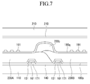
FIG. 7 is a cross-sectional view of a liquid crystal display taken along line VII-VII of FIG. 3.
FIG. 8 is a layout view of a pixel electrode of a liquid crystal display of FIG. 3.
FIG. 9 is a cross-sectional view showing a part of a liquid crystal display according to another embodiment of the present invention.
DETAILED DESCRIPTION OF THE ILLUSTRATED EMBODIMENTS
The present invention is described more fully hereinafter with reference to the accompanying drawings, in which exemplary embodiments of the invention are shown. This invention may, however, be embodied in many different forms and should not be construed as limited to the embodiments set forth herein. Rather, these embodiments are provided so that this disclosure is thorough, and will fully convey the scope of the invention to those skilled in the art. As those skilled in the art will realize, the described embodiments may be modified in various different ways, all without departing from the spirit or scope of the present invention.
In the drawings, the thickness of layers, films, panels, regions, etc., may be exaggerated for clarity. Like reference numerals designate like elements throughout the specification. It will be understood that when an element such as a layer, film, region, or substrate is referred to as being “on” or “connected to” another element, it can be directly on or directly connected to the other element or intervening elements may be present. In contrast, when an element is referred to as being “directly on” or “directly connected to” another element, there are no intervening elements present.
Hereinafter, a liquid crystal display according to an exemplary embodiment of the present invention will be described in brief with reference to FIG. 1.
FIG. 1 is a cross-sectional view schematically showing the structure of a liquid crystal display according to an exemplary embodiment of the present invention.
As shown in FIG. 1, the liquid crystal display according to the exemplary embodiment of the present invention includes a lower display panel 100 and an upper display panel 200 that face each other and a liquid crystal layer 3 interposed therebetween.
The lower display panel 100 includes a substrate 110, a first color filter 230A and a second color filter 230B that are formed on the substrate 110 and are overlapped on each other, a colored member 220 that is formed on the substrate 110 and disposed at an overlap of the first color filter and 230A and the second color filter 230B, an insulating layer 180 disposed on the first color filter 230A, the second color filter 230B and the colored member 220, and a pixel electrode 191 and a spacer 325 that are disposed on the insulating layer 180.
The thickness of a portion of the first color filter 230A that is overlapped with the pixel electrode 191 is greater than the thickness of a portion of the first color filter 230A that is overlapped with the second color filter 230B. Likewise, the thickness of a portion of the second color filter 230B that is overlapped with the pixel electrode 191 is greater than the thickness of a portion of the second color filter 230B that is overlapped with the first color filter 230A.
The upper display panel 200 includes a common electrode 270 formed on the substrate 210.
The height of the colored member 220 disposed on the overlap of the first color filter 230A and the second color filter 230B may be less than that of the spacer 325.
In another embodiment, the spacer 325 may be formed by the same layer as the colored member 220.
Hereinafter, referring to FIG. 2, FIG. 3, FIG. 4, FIG. 5, FIG. 6, FIG. 7, and FIG. 8, a liquid crystal display according to an exemplary embodiment of the present invention will be described in detail. FIG. 2 is an equivalent circuit diagram of one pixel in a liquid crystal display according to an exemplary embodiment of the present invention, FIG. 3 is a layout view of a liquid crystal display according to an exemplary embodiment of the present invention, FIG. 4 is a layout view of a color filter of a liquid crystal display according to an exemplary embodiment of the present invention, FIG. 5 is a cross-sectional view of a liquid crystal display taken along line V-V of FIG. 3, FIG. 6 is a cross-sectional view of a liquid crystal display taken along line VI-VI of FIG. 3, FIG. 7 is a cross-sectional view of a liquid crystal display taken along line VII-VII of FIG. 3, and FIG. 8 is a layout view of a pixel electrode of a liquid crystal display of FIG. 3.
Referring to FIG. 2, the liquid crystal display according to the exemplary embodiment of the present invention includes signal lines including a gate line 121, a sustaining electrode line 125, a voltage drop gate line 123, and a data line 171 and a pixel PX connected with the signal lines.
The pixel PX includes first, second, and third switching elements Qh, Ql, and Qc, first and second liquid crystal capacitors Clch and Clcl, first and second sustaining capacitors Csth and Cstl, and a voltage drop capacitor Cstd. Herein, the first switching element Qh and a first thin film transistor Qh, the second switching element Ql and a second thin film transistor Ql, and the third switching element Qc and a third thin film transistor Qc are each represented by the same reference numeral.
The first switching element Qh and the second switching element Ql are connected to the gate line 121 and the data line 171, and the third switching element Qc is connected to the voltage drop gate line 123.
The first switching element Qh and the second switching element Ql are 3-terminal elements such as a thin film transistor, etc. provided on the lower display panel 100. Control terminals of the first switching element Qh and the second switching element Ql are connected with the gate line 121, input terminals of the first switching element Qh and the second switching element Ql are connected with the data line 171, and output terminals of the first switching element Qh and the second switching element Ql are connected with the first and second liquid crystal capacitors Clch and Clcl and the first and second sustaining capacitors Csth and Cstl, respectively.
The third switching element Qc is also a 3-terminal element such as a thin film transistor, etc. provided on the lower display panel 100 and a control terminal of the third switching element Qc is connected with the voltage drop gate line 123, an input terminal of the third switching element Qc is connected with the second liquid crystal capacitor Clcl, and an output terminal of the third switching element Qc is connected with the voltage drop capacitor Cstd.
Referring to FIG. 3, a first subpixel electrode 191 h connected with the first switching element Qh and the common electrode 270 of the upper display panel 200 (FIG. 5) are overlapped with each other to form the first liquid crystal capacitor Clch. A second subpixel electrode 191 l connected with the second switching element Ql and the common electrode 270 of the upper display panel 200 are overlapped with each other to form the second liquid crystal capacitor Clcl. The first and second sustaining capacitors Csth and Cstl are formed by overlapping the sustaining electrode line 125 including the sustaining electrode 129 with the first and second subpixel electrodes 191 h and 191 l.
The voltage drop capacitor Cstd is connected with the output terminal of the third switching element Qc and the sustaining electrode line 125 and is formed by overlapping the sustaining electrode line 125 and the output terminal of the third switching element Qc that are provided on the lower display panel 100 with each other with an insulator interposed therebetween.
Hereinafter, referring to FIG. 3, FIG. 4, FIG. 5, FIG. 6, FIG. 7 and FIG. 8, the liquid crystal display shown in FIG. 2 will be described in more detail.
The liquid crystal display according to the exemplary embodiment of the present invention includes the lower display panel 100 and the upper display panel 200 that face each other, the liquid crystal layer 3 interposed between the two display panels 100 and 200, and a pair of polarizers (not shown) attached to outer surfaces of the display panels 100 and 200.
First, the lower display panel 100 will be described.
A plurality of gate conductors including a plurality of gate lines 121, a plurality of voltage drop gate lines 123, and a plurality of sustaining electrode lines 125 are formed on an insulating substrate 110.
The gate lines 121 and the voltage drop gate lines 123 primarily extend in a transverse direction and transmit a gate signal. The gate line 121 includes a first gate electrode 124 h and a second gate electrode 124 l that vertically protrude and the voltage drop gate line 123 includes a third gate electrode 124 c that protrudes upward. The first gate electrode 124 h and the second gate electrode 124 l are connected with each other to form one protrusion.
The sustaining electrode line 125 also extends primarily in the transverse direction and transmits predetermined voltage such as common voltage Vcom, etc. The sustaining electrode line 125 includes a sustaining electrode 135 extending vertically, a pair of vertical portions 128 extending downward substantially in a vertical direction toward the gate line 121, and a transverse portion 127 connecting ends of the pair of vertical portions 128 with each other. The transverse portion 127 includes a capacitive electrode 126 extending downward.
A gate insulating layer 140 is formed on the gate conductors 121, 123, 125.
A plurality of linear semiconductors 151 that may be made of amorphous or crystalline silicon, etc. are formed on the gate insulating layer 140. The linear semiconductor 151 extends primarily in the vertical direction and includes the first and second semiconductors 154 h and 154 l that extend toward the first and second gate electrodes 124 h and 124 l and are connected with each other and a third semiconductor 154 c connected with the second semiconductor 154 l. The third semiconductor 154 c extends to form a fourth semiconductor 157.
A plurality of linear ohmic contacts (not shown) are formed on the linear semiconductor 151, a first ohmic contact (not shown) is formed on the first semiconductor 154 h, and a second ohmic contact 164 b and a third ohmic contact (not shown) are formed evenly on the second semiconductor 154 l and the third semiconductor 154 c. The linear ohmic contact includes a first protrusion (not shown) disposed on a first protrusion of the semiconductor by forming a pair with a first island-type ohmic contact, a second protrusion (not shown) disposed on a second protrusion of the semiconductor by forming a pair with a second island-type ohmic contact, and a third protrusion (not shown) disposed on a third protrusion of the semiconductor by forming a pair with a third island-type ohmic contact. The third ohmic contact extends to form a fourth ohmic contact 167.
A data conductor including the plurality of data lines 171, a plurality of first drain electrodes 175 h, a plurality of second drain electrodes 175 l, and a plurality of third drain electrodes 175 c is formed on the ohmic contacts 164 b and 167.
The data lines 171 transmit data signals and extend primarily in the vertical direction to cross the gate line 121 and the voltage drop gate line 123. Each data line 171 includes a first source electrode 173 h and a second source electrode 173 l that extend toward the first gate electrode 124 h and the second gate electrode 124 l to form a ‘un’ shape together.
Each of the first drain electrode 175 h, the second drain electrode 175 l, and the third drain electrode 175 c includes one wide end and the other bar-type end. The bar-type end of each of the first drain electrode 175 h and the second drain electrode 175 l is partially surrounded by the first source electrode 173 h and the second source electrode 173 l. The wide end of the second drain electrode 175 l extends again to form the third source electrode 173 c bent in a ‘U’ shape. The wide end 177 c of the third drain electrode 175 c is overlapped with the capacitive electrode 126 to form the voltage drop capacitor Cstd and the bar-type end is partially surrounded by the third source electrode 173 c.
The first, second, and third gate electrodes 124 h, 124 l, and 124 c, the first, second, and third source electrodes 173 h, 173 l, and 173 c, and the first, second, and third drain electrodes 175 h, 175 l, and 175 c form the first, second, and third thin film transistors (TFTs) Qh, Ql, and Qc together with the first, second, and third island- shape semiconductors 154 h, 154 l, and 154 c, respectively. A channel of the thin film transistor is formed in each of the semiconductors 154 h, 154 l, and 154 c between each of the source electrodes 173 h, 173 l, and 173 c, and each of the drain electrodes 175 h, 175 l, and 175 c.
The linear semiconductor 151 including the semiconductors 154 h, 154 l, and 154 c has substantially the same planar shape as the data conductors 171, 175 h, 175 l, and 175 c and the ohmic contacts 164 b and 167 below the data conductors except for a channel area between the source electrodes 173 h, 173 l, and 173 c and the drain electrodes 175 h, 175 l, and 175 c. That is, an exposed part without being covered by the data conductors 171, 175 h, 175 l, and 175 c is provided in addition to parts between the source electrodes 173 h, 173 l, and 173 c and the drain electrodes 175 h, 175 l, and 175 c in the linear semiconductor 151 including the semiconductors 154 h, 154 l, and 154 c.
A lower passivation layer 180 p that may be made of an inorganic insulating material such as silicon nitride or silicon oxide is formed on the data conductors 171, 175 h, 175 l, and 175 c and the exposed part of the semiconductors 154 h, 154 l, and 154 c.
The first color filter 230A and the second color filter 230B are located on the lower passivation layer 180 p. As shown in FIG. 4, each of the color filters 230A and 230B is located in most of the area except for areas at which the first thin film transistor Qh, the second thin film transistor Ql, and the third transistor Qc are located. Parts of the first color filter 230A and the second color filter 230B, which extend in the vertical direction between the adjacent data lines 171 are overlapped with each other. The part where the first color filter 230A and the second color filter 230B are overlapped with each other may be overlapped with at least a part of the data line 171. Each of the color filters 230A and the 230B may display any one of primary colors including three primary colors such as red, green, and blue colors, etc. For each color filter 230A and 230B, the thickness of the overlapped part where the first color filter 230A and the second color filter 230B are overlapped with each other may be less than the thickness of the rest of the color filter part. The width of the part where the first color filter 230A and the second color filter 230B are overlapped with each other is preferably greater than or equal to approximately 7 μm.
The colored member 220 is located on an area where the color filters 230A and 230B are not located and the area where the first color filter 230A and the second color filter 230B are overlapped with each other. The colored member 220 extends vertically on the gate line 121 and the voltage drop gate line 123 and includes a first colored member 220 a covering an area where the first thin film transistor Qh, the second thin film transistor Ql, and the third thin film transistor Qc are located and a second colored member 220 b extending on the data line 171. The height of a part of the second colored member 220 b, which is disposed on the first color filter 230A and the second color filter 230B overlapped with each other is greater than those of the rest of the parts of the colored member 220. This will be described in detail.
Referring to FIG. 6 and FIG. 7, the height of the second colored member 220 b disposed on the part between the first color filter 230A and the second color filter 230B, which are not overlapped with each other is less than the height of the second colored member 220 b disposed on the first color filter 230A and the second color filter 230B there. That is, the second colored member 220 b disposed on the first color filter 230A and the second color filter 230B extending on two adjacent data lines 171 is higher than that of the colored member 220 disposed between the first color filter 230A and the second color filter 230B that are not overlapped with each other.
Since the width of the part where the first color filter 230A and the second color filter 230B are overlapped with each other should be approximately 7 μm or more, the colored member 220 may be stably disposed to have a predetermined height.
The colored member 220 may include a black pigment, etc. and prevents light leakage. The colored member 220 may be referred to as a black matrix.
An upper passivation layer 180 q is formed on the color filter 230 and the colored member 220. The upper passivation layer 180 q prevents the color filter 230 and the colored member 220 from getting loose and suppresses contamination of the liquid crystal layer 3 due to an organic material such as a solvent introduced from the color filter 230 to prevent a defect such as an afterimage which may be caused in driving a screen.
A plurality of first contact holes 185 h and a plurality of second contact holes 185 l that expose the wide end of the first drain electrode 175 h and the wide end of the second drain electrode 175 l, respectively are formed in the lower passivation layer 180 p, the colored member 220, and the upper passivation layer 180 q.
A plurality of pixel electrodes 191 are formed on the upper passivation layer 180 q.
Referring to FIG. 3, the pixel electrodes 191 include a first subpixel electrode 191 h and a second subpixel electrode 191 l that are separated from each other with two gate lines 121 and 123 interposed therebetween, are disposed at upper and lower portions of a pixel area around the gate lines 121 and 123 and are adjacent to each other in a column direction. Each of the first subpixel electrode 191 h and the second subpixel 191 l includes a basic electrode 199 shown in FIG. 8 or at least one modification thereof.
The thickness of the overlap between the color filters 230A and 230B is thicker than those of the parts where the color filters 230A and the 230B are overlapped with the pixel electrode 191.
Hereinafter, referring to FIG. 8, the basic electrode 199 will be described in detail.
As shown in FIG. 8, the basic electrode 199 has an overall rectangular shape and includes a cross stem portion constituted by a transverse stem portion 193 and a vertical stem portion 192 orthogonal thereto. Further, the basic electrode 199 is divided into a first subarea Da, a second subarea Db, a third subarea Dc, and a fourth subarea Dd by the transverse stem portion 193 and the vertical stem portion 192 and each of the subareas Da, Db, Dc and Dd includes a plurality of first, second, third and fourth minute branch portions 194 a, 194 b, 194 c, and 194 d, respectively.
The first minute branch portion 194 a extends obliquely to an upper left direction from the transverse stem portion 193 or the vertical stem portion 192 and the second minute branch portion 194 b extends obliquely to an upper right direction from the transverse stem portion 193 or the vertical stem portion 192. Further, the third minute branch portion 194 c extends obliquely to a lower left direction from the transverse stem portion 193 or the vertical stem portion 192 and the fourth minute branch portion 194 d extends obliquely to a lower right direction from the transverse stem portion 193 or the vertical stem portion 192
The first to fourth minute branch portions 194 a, 194 b, 194 c, and 194 d form an angle of approximately 45 degrees or 135 degrees with the gate lines 121 a and the 121 b or the transverse stem portion 193. Further, the minute branch portions 194 a, 194 b, 194 c, and 194 d of the adjacent four subareas Da, Db, Dc, and Dd may be orthogonal to each other.
The widths of the minute branch portions 194 a, 194 b, 194 c, and 194 d may be in the range of 2.5 to 5.0 μm and a gap between the adjacent minute branch portions 194 a, 194 b, 194 c, and 194 d in one subarea Da, Db, Dc, or Dd may be in the range of 2.5 to 5.0 μm.
According to another embodiment of the present invention, the widths of the minute branch portions 194 a, 194 b, 194 c, and 194 d may be wider as the minute branch portions are closer to the transverse stem portion 193 or the vertical stem portion 192. Further, a difference between the widest portion and the narrowest portion in one minute branch portion 194 a, 194 b, 194 c, or 194 d may be in the range of 0.2 to 1.5 μm.
The first subpixel electrode 191 h and the second subpixel electrode 191 l include outer stem portions surrounding outer edges and vertical portions of the outer stem portions extend on the data line 171 to prevent capacitive coupling between the data line 171 and the first subpixel electrode 191 h and the second subpixel electrode 191 l.
The first subpixel electrode 191 h and the second subpixel electrode 191 l are applied with receive data voltage from the first drain electrode 175 h and the second drain electrode 175 l through the first contact hole 185 h and the second contact hole 185 l, respectively. The first subpixel electrode 191 h and the second subpixel electrode 191 l applied with the data voltage generate an electric field together with the common electrode of the common electrode display panel 200 so as to determine orientation of liquid crystal molecules of the liquid crystal layer 3 between two electrodes 191 and 270. The luminance of light passing through the liquid crystal layer 3 depends on the orientation of the liquid crystal molecules determined as above.
Sides of the first to fourth minute branch portions 194 a, 194 b, 194 c, and 194 d distort the electric field to form horizontal components for determining inclined directions of the liquid crystal molecules 31. The horizontal components of the electric field are substantially horizontal to the sides of the first to fourth minute branch portions 194 a, 194 b, 194 c, and 194 d. As a result, as shown in FIG. 8, the liquid crystal molecules 31 are inclined in a direction parallel to longitudinal directions of the minute branch portions 194 a, 194 b, 194 c, and 194 d. One pixel electrode 191 includes four subareas Da to Dd in which the longitudinal directions of the minute branch portions 194 a, 194 b, 194 c, and 194 d are different from each other. Therefore, the liquid crystal molecules 31 are inclined in four different directions and four domains of which the liquid crystal molecules 31 have different orientation directions are formed on the liquid crystal layer 3. As such, when the liquid crystal molecules are inclined in various directions, a reference viewing angle of the liquid crystal display is increased.
The first subpixel electrode 191 h and the common electrode 270 form the first liquid crystal capacitor Clch together with the liquid crystal layer 3 interposed therebetween and the second subpixel electrode 191 l and the common electrode 270 form the second liquid crystal capacitor Clcl together with the liquid crystal layer 3 interposed therebetween to maintain applied voltage even after the first thin film transistor Qh and the second thin film transistor Ql are turned off.
The first and second subpixel electrodes 191 h and 191 l are overlapped with the sustaining electrode line 125 including the sustaining electrode 129 to form the first and second sustaining capacitors Csth and Cstl and the first and second sustaining capacitors Csth and Cstl strengthens voltage sustaining capacities of the first and second liquid crystal capacitors Clch and Clcl, respectively.
The capacitive electrode 126 and an extension portion 177 c of the third drain electrode 175 c are overlapped with each other with the gate insulating layer 140 and the fourth semiconductor layer 157 and the fourth ohmic contact layer 167 interposed therebetween to form the voltage drop capacitor Cstd. In another embodiment of the present invention, the fourth semiconductor layer 157 and the fourth ohmic contact layer 167 may be removed, which are disposed between the capacitive electrode 126 and the extension portion 177 c of the third drain electrode 175 c forming the voltage drop capacitor Cstd.
The spacer 325 is formed on the upper passivation layer 180 q. The spacer 325 maintains a constant cell gap of the liquid crystal layer 3 disposed between the lower display panel 100 and the upper display panel 200. In another embodiment, the spacer 325 may be formed by the same layer as the colored member 220.
Although not shown, the spacer 325 may include a first spacer and a second spacer that have different heights. The heights of the first spacer and the second spacer are greater than that of the colored member 220. The spacer having the greater height between the first spacer and the second spacer serves to maintain the cell gap and the second spacer serves to maintain the cell gap when elasticity of the first spacer is damaged due to external pressure.
The part of the colored member 220 disposed on the first color filter 230A and the second color filter 230B that are overlapped with each other among the above-mentioned colored member 220 parts may have a height less than the spacer 325 and a difference in height between the colored member 220 and the spacer 325 may be approximately 2.0 μm or less and more specifically, may be less than approximately 1.4 μm.
The part of the colored member 220 disposed on the first color filter 230A and the second color filter 230B that are overlapped with each other among the colored member 220 parts may have a height less than the spacer 325, but greater than other thin film structures. Therefore, the colored member 220 may serve as a subspacer that prevents a smear defect from being generated due to a damage of the elasticity of the spacer 325, which is caused by the external pressure by supporting two display panels when a user applies pressure to a local portion at the time of using the liquid crystal display.
Since the colored member 220 disposed on the first color filter 230A and the second color filter 230B that are overlapped with each other among the colored member 220 may have the height smaller than the first spacer and the second spacer, the colored member may serve to support the liquid crystal layer when pressure higher than pressure for the second spacer to sustain is applied to the second spacer and the liquid crystal cell gap becomes thus narrowed.
Likewise, three or more spacers having different heights which maintain the liquid crystal cell gap are formed to thereby stably maintain the liquid crystal cell even under the external pressure.
A lower orientation layer (not shown) is formed on the pixel electrode 191, the exposed upper passivation layer 180 q, and the spacer 325. The lower orientation layer may be a vertical orientation layer.
Hereinafter, the upper display panel 200 will be described.
The common electrode 270 is formed on the insulating substrate 210. An upper orientation layer (not shown) is formed on the common electrode 270. The upper orientation layer may be the vertical orientation layer.
A polarizer of a pair of polarizers (not shown) is provided on each outer surface of the two display panels 100 and 200. It is preferable that transmission axes of the two polarizers are orthogonal to each other and any one transmission axis of them is parallel to the gate line 121.
The liquid crystal layer 3 has negative permittivity anisotropy and the liquid crystal molecules of the liquid crystal layer 3 are oriented to have long axes vertical to the surfaces of the two display panels 100 and 200 under the condition of no electric field. Accordingly, incident light does not pass through the orthogonal polarizer and is blocked under the condition of no electric field.
As described above, the first subpixel electrode 191 h and the second subpixel electrode 191 l applied with the data voltage generate the electric field together with the common electrode 270 of the common electrode display panel 200, such that the liquid crystal molecules of the liquid crystal layer 3 oriented to be vertical to the surfaces of the two electrodes 191 and 270 under the condition of no electric field lie in a direction horizontal to the surfaces of the two electrodes 191 and 270 and the luminance of the light passing through the liquid crystal layer 3 depends on the lying angles of the liquid crystal molecules.
Like this, in the liquid crystal display according to the exemplary embodiment of the present invention, a high step is formed by partially overlapping adjacent two color filters with each other and a colored member is formed on the step, such that the colored member may be used as a light shielding member for preventing light leakage and a subspacer for preventing a smear defect from being generated. Accordingly, it is possible to prevent the smear defect while constantly maintaining a cell gap of the liquid crystal display without an additional process for manufacturing the subspacer and in addition, it is possible to prevent light leakage between pixels.
Hereinafter, a liquid crystal display according to another embodiment of the present invention will be described with reference to FIG. 9. FIG. 9 is a cross-sectional view showing a part of a liquid crystal display according to another embodiment of the present invention. FIG. 9A is a cross-sectional view showing two color filters not overlapped with each other and FIG. 9B is a cross-sectional view showing two color filters overlapped with each other.
In the embodiment, when the color filters are formed, by exposing an edge of an overlap of the color filters with a halftone mask such as a slit mask, etc., the overlap may have an edge more gentle than an edge of portions of the color filters that are not overlapped with each other and the thicknesses of the color filters may be decreased. By this configuration, since a cross section W of the overlap of the color filters is increased and the surfaces of the color filters may be flattened, an area of a region in which a colored member used as a subspacer for preventing a smear defect may be disposed is increased and the colored member may be stably disposed. Accordingly, it is possible to prevent the position of the subspacer from being changed due to an alignment error, etc.
It will be apparent to those skilled in the art that various modifications and variations can be made in the present invention without departing from the spirit or scope of the invention. Thus, it is intended that the present invention cover the modifications and variations of this invention provided they come within the scope of the appended claims and their equivalents.

Claims (27)

1. A liquid crystal display, comprising:
a first substrate;
a first color filter and a second color filter disposed on the first substrate;
a colored member disposed on the first color filter and the second color filter; and
a pixel electrode disposed on the first color filter and the second color filter,
wherein the first color filter and the second color filter are partially overlapped with each other,
wherein the thickness of the first color filter and the thickness of the second color filter at an overlap between the first color filter and the second color filter are less than the thickness of the first color filter and the thickness of the second color filter at an overlap between the respective color filters and the pixel electrode, and
wherein a maximum height on the first substrate of a first portion of the colored member disposed at the overlap between the first color filter and the second color filter is greater than a maximum height on the first substrate of a second portion of the colored member disposed not at the overlap between the first color filter and the second color filter.
2. The liquid crystal display of claim 1, wherein:
the surface of the overlap where the first color filter and the second color filter are overlapped with each other is flat.
3. The liquid crystal display of claim 2, wherein:
the width of the overlap of the first color filter and the second color filter is greater than or equal to approximately 7 μm.
4. The liquid crystal display of claim 3, further comprising:
a spacer for maintaining a cell gap,
wherein the height of the colored member is less than the height of the spacer.
5. The liquid crystal display of claim 4, wherein:
a difference in height between the colored member and the spacer is less than or equal to approximately 2 μm.
6. The liquid crystal display of claim 5, wherein:
the difference in height between the colored member and the spacer is less than or equal to approximately 1.4 μm.
7. The liquid crystal display of claim 4, wherein:
the spacer and the colored member are formed of the same layer.
8. The liquid crystal display of claim 4, wherein:
the spacer comprises a first spacer and a second spacer that have different heights from each other, and
the colored member has a height less than a height of the first spacer and a height of the second spacer.
9. The liquid crystal display of claim 4, further comprising:
a first signal line disposed on the first substrate,
wherein the overlap of the first color filter and the second color filter is partially overlapped with the first signal line.
10. The liquid crystal display of claim 9, wherein:
the first signal line comprises a data line.
11. A liquid crystal display, comprising:
a first substrate;
a first color filter and a second color filter disposed on the first substrate;
a colored member disposed on the first color filter and the second color filter; and
a pixel electrode disposed on the first color filter and the second color filter,
wherein the first color filter and the second color filter are partially overlapped with each other
wherein the thickness of the first color filter and the thickness of the second color filter at an overlap between the first color filter and the second color filter are less than the thickness of the first color filter and the thickness of the second color filter at an overlap between the respective color filters and the pixel electrode,
wherein the height of the colored member disposed at the overlap between the first color filter and the second color filter is greater than the height of the colored member disposed not at the overlap between the first color filter and the second color filter; and
wherein the width of the overlap of the first color filter and the second color filter is greater than or equal to approximately 7 μm.
12. The liquid crystal display of claim 11, further comprising:
a spacer to maintain a cell gap,
wherein the height of the colored member is less than a height of the spacer.
13. The liquid crystal display of claim 12, wherein:
a difference in height between the colored member and the spacer is less than or equal to approximately 2 μm.
14. The liquid crystal display of claim 13, wherein:
the difference in height between the colored member and the spacer is less than or equal to approximately 1.4 μm.
15. The liquid crystal display of claim 12, wherein:
the spacer and the colored member are formed of the same layer.
16. The liquid crystal display of claim 12, wherein:
the spacer comprises a first spacer and a second spacer that have different heights from each other, and
the colored member has a height less than a height of the first spacer and a height of the second spacer.
17. The liquid crystal display of claim 12, further comprising:
a first signal line disposed on the first substrate,
wherein the overlap of the first color filter and the second color filter is partially overlapped with the first signal line.
18. The liquid crystal display of claim 17, wherein:
the first signal line comprises a data line.
19. The liquid crystal display of claim 1, further comprising:
a spacer to maintain a cell gap,
wherein the height of the colored member is less than a height of the spacer.
20. A liquid crystal display, comprising:
a first substrate;
a first color filter and a second color filter disposed on the first substrate;
a colored member disposed on the first color filter and the second color filter;
a pixel electrode disposed on the first color filter and the second color filter; and
a spacer to maintain a cell gap,
wherein the height of the colored member is less than a height of the spacer,
wherein the first color filter and the second color filter are partially overlapped with each other
wherein the thickness of the first color filter and the thickness of the second color filter at an overlap between the first color filter and the second color filter are less than the thickness of the first color filter and the thickness of the second color filter at an overlap between the respective color filters and the pixel electrode,
wherein the height of the colored member disposed at the overlap between the first color filter and the second color filter is greater than the height of the colored member disposed not at the overlap between the first color filter and the second color filter, and
wherein a difference in height between the colored member and the spacer is less than or equal to approximately 2 μm.
21. The liquid crystal display of claim 20, wherein:
the difference in height between the colored member and the spacer is less than or equal to approximately 1.4 μm.
22. The liquid crystal display of claim 19, wherein:
the spacer and the colored member are formed of the same layer.
23. The liquid crystal display of claim 19, wherein:
the spacer comprises a first spacer and a second spacer that have different heights from each other, and
the colored member has a height less than a height of the first spacer and a height of the second spacer.
24. The liquid crystal display of claim 19, further comprising:
a first signal line disposed on the first substrate,
wherein the overlap of the first color filter and the second color filter is partially overlapped with the first signal line.
25. The liquid crystal display of claim 24, wherein:
the first signal line comprises a data line.
26. The liquid crystal display of claim 1, further comprising:
a first signal line disposed on the first substrate,
wherein the overlap of the first color filter and the second color filter is partially overlapped with the first signal line.
27. The liquid crystal display of claim 26, wherein:
the first signal line comprises a data line.
US12/900,433 2010-03-05 2010-10-07 Liquid crystal display Active 2031-07-22 US8400588B2 (en)

Applications Claiming Priority (2)

Application Number Priority Date Filing Date Title
KR1020100019885A KR101669238B1 (en) 2010-03-05 2010-03-05 Liquid crystal display
KR10-2010-0019885 2010-03-05

Publications (2)

Publication Number Publication Date
US20110216276A1 US20110216276A1 (en) 2011-09-08
US8400588B2 true US8400588B2 (en) 2013-03-19

Family

ID=44531054

Family Applications (1)

Application Number Title Priority Date Filing Date
US12/900,433 Active 2031-07-22 US8400588B2 (en) 2010-03-05 2010-10-07 Liquid crystal display

Country Status (2)

Country Link
US (1) US8400588B2 (en)
KR (1) KR101669238B1 (en)

Cited By (1)

* Cited by examiner, † Cited by third party
Publication number Priority date Publication date Assignee Title
US20150253608A1 (en) * 2014-03-10 2015-09-10 Lg Display Co., Ltd. Liquid crystal display device

Families Citing this family (18)

* Cited by examiner, † Cited by third party
Publication number Priority date Publication date Assignee Title
KR20130112628A (en) 2012-04-04 2013-10-14 삼성디스플레이 주식회사 Liquid crystal display
KR101965304B1 (en) * 2012-06-07 2019-08-14 삼성디스플레이 주식회사 Liquid crystal display and method for manufacturing the same
KR101965305B1 (en) * 2012-08-17 2019-04-04 삼성디스플레이 주식회사 Liquid crystal display and method for manufacturing the same
KR102082406B1 (en) 2012-10-05 2020-02-28 삼성디스플레이 주식회사 Liquid crystal display
KR102032962B1 (en) 2012-10-26 2019-10-17 삼성디스플레이 주식회사 Thin film transistor array substrate and manufacturing method thereof
KR20140147299A (en) * 2013-06-19 2014-12-30 삼성디스플레이 주식회사 Curved display device and manufacturing method thereof
KR20150085349A (en) 2014-01-15 2015-07-23 삼성디스플레이 주식회사 Display apparatus and fabrication method thereof
KR102189578B1 (en) * 2014-07-30 2020-12-14 삼성디스플레이 주식회사 Liquid crystal display panel and manufacturing method thereof
KR102238416B1 (en) 2014-11-17 2021-04-12 삼성디스플레이 주식회사 Array substrate and Manufacturing Method thereof
KR20160073689A (en) * 2014-12-17 2016-06-27 삼성디스플레이 주식회사 Liquid crystal display device
KR102276698B1 (en) * 2014-12-26 2021-07-13 삼성디스플레이 주식회사 Array substrate for display device
KR102281844B1 (en) * 2015-01-02 2021-07-26 삼성디스플레이 주식회사 Liquid crystal display and method for manufacturing the same
KR20160090974A (en) 2015-01-22 2016-08-02 삼성디스플레이 주식회사 Liquid crystal display device
KR102334808B1 (en) 2015-04-30 2021-12-03 삼성디스플레이 주식회사 Display panel
KR20160135888A (en) * 2015-05-18 2016-11-29 삼성디스플레이 주식회사 Display device
KR102340266B1 (en) * 2015-08-06 2021-12-16 삼성디스플레이 주식회사 Display device
CN110687704B (en) * 2019-10-23 2022-09-27 Tcl华星光电技术有限公司 Method for detecting factors influencing splicing exposure defects of COA substrate
CN112216210B (en) * 2020-10-14 2022-10-14 厦门天马微电子有限公司 Color film substrate, display panel and display device

Citations (6)

* Cited by examiner, † Cited by third party
Publication number Priority date Publication date Assignee Title
US5623353A (en) * 1990-10-26 1997-04-22 Ricoh Company, Ltd. Color liquid crystal device having thickness controlling layers disposed at pixel portions
US6671025B1 (en) * 1999-02-15 2003-12-30 Fujitsu Display Technologies Corporation Liquid crystal display device and method of manufacturing the same without scattering spacers
KR20040061230A (en) 2002-12-30 2004-07-07 엘지.필립스 엘시디 주식회사 Liquid Crystal Display and Method of Fabricating the same
JP2007286384A (en) 2006-04-18 2007-11-01 Sharp Corp Liquid crystal display device
JP2008026812A (en) 2006-07-25 2008-02-07 Toppan Printing Co Ltd Color filter and method for manufacturing the same
US20090167973A1 (en) * 2007-12-27 2009-07-02 Sun-Young Chang Thin film transistor array panel and method for manufacturing the same, and liquid crystal display

Family Cites Families (3)

* Cited by examiner, † Cited by third party
Publication number Priority date Publication date Assignee Title
JP2000111724A (en) * 1998-10-02 2000-04-21 Sharp Corp Color filter, production of color filter and liquid crystal display device using it
KR101380435B1 (en) * 2007-03-07 2014-04-02 엘지디스플레이 주식회사 Liquid crystal display and method for manufacturing the same
KR101499229B1 (en) * 2008-04-07 2015-03-05 삼성디스플레이 주식회사 Display device including color filters

Patent Citations (6)

* Cited by examiner, † Cited by third party
Publication number Priority date Publication date Assignee Title
US5623353A (en) * 1990-10-26 1997-04-22 Ricoh Company, Ltd. Color liquid crystal device having thickness controlling layers disposed at pixel portions
US6671025B1 (en) * 1999-02-15 2003-12-30 Fujitsu Display Technologies Corporation Liquid crystal display device and method of manufacturing the same without scattering spacers
KR20040061230A (en) 2002-12-30 2004-07-07 엘지.필립스 엘시디 주식회사 Liquid Crystal Display and Method of Fabricating the same
JP2007286384A (en) 2006-04-18 2007-11-01 Sharp Corp Liquid crystal display device
JP2008026812A (en) 2006-07-25 2008-02-07 Toppan Printing Co Ltd Color filter and method for manufacturing the same
US20090167973A1 (en) * 2007-12-27 2009-07-02 Sun-Young Chang Thin film transistor array panel and method for manufacturing the same, and liquid crystal display

Cited By (2)

* Cited by examiner, † Cited by third party
Publication number Priority date Publication date Assignee Title
US20150253608A1 (en) * 2014-03-10 2015-09-10 Lg Display Co., Ltd. Liquid crystal display device
US9823521B2 (en) * 2014-03-10 2017-11-21 Lg Display Co., Ltd. Apparatus and liquid crystal display device with column spacers

Also Published As

Publication number Publication date
US20110216276A1 (en) 2011-09-08
KR20110100842A (en) 2011-09-15
KR101669238B1 (en) 2016-10-26

Similar Documents

Publication Publication Date Title
US8400588B2 (en) Liquid crystal display
US8767147B2 (en) Liquid crystal display wherein a first light blocking portion and a first colored portion extends generally along a gate line and generally covers the gate line and a thin film transistor
US9791748B2 (en) Liquid crystal display
US9417498B2 (en) Liquid crystal display
US8455870B2 (en) Thin film transistor array panel and method of manufacturing the same
US9298044B2 (en) Liquid crystal display
JP4946135B2 (en) Liquid crystal display element
US9519194B2 (en) Liquid crystal display
US9612464B2 (en) Liquid crystal display
US20150092132A1 (en) Thin film transistor array panel, liquid crystal display and manufacturing method of thin film transistor array panel
US8111364B2 (en) In-plane switching mode liquid crystal display capable of improving an aperture ratio and fabrication method thereof
US20110090446A1 (en) Display device
US20150077678A1 (en) Liquid crystal display
US8582044B2 (en) Liquid crystal display and repairing method thereof
US8304768B2 (en) Thin film transistor array substrate and method for manufacturing the same
US10754213B2 (en) Thin film transistor substrate
US9494838B2 (en) Liquid crystal display device
JPH03198030A (en) Thin film transistor panel
US20090147189A1 (en) Display panel
US8895439B2 (en) Method for forming pattern and method for manufacturing display device by using the same
TWI670551B (en) Liquid crystal display device
KR20080002434A (en) Array substrate for liquid crystal panel and fabricating methode thereof
KR20160122098A (en) Liquid crystal display

Legal Events

Date Code Title Description
AS Assignment

Owner name: SAMSUNG ELECTRONICS CO., LTD., KOREA, REPUBLIC OF

Free format text: ASSIGNMENT OF ASSIGNORS INTEREST;ASSIGNORS:YANG, BYUNG-DUK;LEE, EUN-GUK;KWAK, SANG-KI;AND OTHERS;REEL/FRAME:025110/0942

Effective date: 20101007

AS Assignment

Owner name: SAMSUNG DISPLAY CO., LTD., KOREA, REPUBLIC OF

Free format text: CHANGE OF NAME;ASSIGNOR:SAMSUNG ELECTRONICS CO., LTD.;REEL/FRAME:028859/0868

Effective date: 20120403

FEPP Fee payment procedure

Free format text: PAYOR NUMBER ASSIGNED (ORIGINAL EVENT CODE: ASPN); ENTITY STATUS OF PATENT OWNER: LARGE ENTITY

STCF Information on status: patent grant

Free format text: PATENTED CASE

FPAY Fee payment

Year of fee payment: 4

MAFP Maintenance fee payment

Free format text: PAYMENT OF MAINTENANCE FEE, 8TH YEAR, LARGE ENTITY (ORIGINAL EVENT CODE: M1552); ENTITY STATUS OF PATENT OWNER: LARGE ENTITY

Year of fee payment: 8