US8390551B2 - Driving device for quickly changing the gray level of the liquid crystal display and its driving method - Google Patents
Driving device for quickly changing the gray level of the liquid crystal display and its driving method Download PDFInfo
- Publication number
- US8390551B2 US8390551B2 US12/140,674 US14067408A US8390551B2 US 8390551 B2 US8390551 B2 US 8390551B2 US 14067408 A US14067408 A US 14067408A US 8390551 B2 US8390551 B2 US 8390551B2
- Authority
- US
- United States
- Prior art keywords
- thin film
- gate lines
- gate
- film transistors
- liquid crystal
- Prior art date
- Legal status (The legal status is an assumption and is not a legal conclusion. Google has not performed a legal analysis and makes no representation as to the accuracy of the status listed.)
- Active, expires
Links
Images


Classifications
-
- G—PHYSICS
- G09—EDUCATION; CRYPTOGRAPHY; DISPLAY; ADVERTISING; SEALS
- G09G—ARRANGEMENTS OR CIRCUITS FOR CONTROL OF INDICATING DEVICES USING STATIC MEANS TO PRESENT VARIABLE INFORMATION
- G09G3/00—Control arrangements or circuits, of interest only in connection with visual indicators other than cathode-ray tubes
- G09G3/20—Control arrangements or circuits, of interest only in connection with visual indicators other than cathode-ray tubes for presentation of an assembly of a number of characters, e.g. a page, by composing the assembly by combination of individual elements arranged in a matrix no fixed position being assigned to or needed to be assigned to the individual characters or partial characters
- G09G3/34—Control arrangements or circuits, of interest only in connection with visual indicators other than cathode-ray tubes for presentation of an assembly of a number of characters, e.g. a page, by composing the assembly by combination of individual elements arranged in a matrix no fixed position being assigned to or needed to be assigned to the individual characters or partial characters by control of light from an independent source
- G09G3/36—Control arrangements or circuits, of interest only in connection with visual indicators other than cathode-ray tubes for presentation of an assembly of a number of characters, e.g. a page, by composing the assembly by combination of individual elements arranged in a matrix no fixed position being assigned to or needed to be assigned to the individual characters or partial characters by control of light from an independent source using liquid crystals
- G09G3/3611—Control of matrices with row and column drivers
- G09G3/3648—Control of matrices with row and column drivers using an active matrix
-
- G—PHYSICS
- G09—EDUCATION; CRYPTOGRAPHY; DISPLAY; ADVERTISING; SEALS
- G09G—ARRANGEMENTS OR CIRCUITS FOR CONTROL OF INDICATING DEVICES USING STATIC MEANS TO PRESENT VARIABLE INFORMATION
- G09G2300/00—Aspects of the constitution of display devices
- G09G2300/08—Active matrix structure, i.e. with use of active elements, inclusive of non-linear two terminal elements, in the pixels together with light emitting or modulating elements
- G09G2300/0809—Several active elements per pixel in active matrix panels
-
- G—PHYSICS
- G09—EDUCATION; CRYPTOGRAPHY; DISPLAY; ADVERTISING; SEALS
- G09G—ARRANGEMENTS OR CIRCUITS FOR CONTROL OF INDICATING DEVICES USING STATIC MEANS TO PRESENT VARIABLE INFORMATION
- G09G2310/00—Command of the display device
- G09G2310/02—Addressing, scanning or driving the display screen or processing steps related thereto
- G09G2310/0202—Addressing of scan or signal lines
- G09G2310/0205—Simultaneous scanning of several lines in flat panels
-
- G—PHYSICS
- G09—EDUCATION; CRYPTOGRAPHY; DISPLAY; ADVERTISING; SEALS
- G09G—ARRANGEMENTS OR CIRCUITS FOR CONTROL OF INDICATING DEVICES USING STATIC MEANS TO PRESENT VARIABLE INFORMATION
- G09G2310/00—Command of the display device
- G09G2310/02—Addressing, scanning or driving the display screen or processing steps related thereto
- G09G2310/0202—Addressing of scan or signal lines
- G09G2310/0218—Addressing of scan or signal lines with collection of electrodes in groups for n-dimensional addressing
-
- G—PHYSICS
- G09—EDUCATION; CRYPTOGRAPHY; DISPLAY; ADVERTISING; SEALS
- G09G—ARRANGEMENTS OR CIRCUITS FOR CONTROL OF INDICATING DEVICES USING STATIC MEANS TO PRESENT VARIABLE INFORMATION
- G09G2310/00—Command of the display device
- G09G2310/02—Addressing, scanning or driving the display screen or processing steps related thereto
- G09G2310/0232—Special driving of display border areas
-
- G—PHYSICS
- G09—EDUCATION; CRYPTOGRAPHY; DISPLAY; ADVERTISING; SEALS
- G09G—ARRANGEMENTS OR CIRCUITS FOR CONTROL OF INDICATING DEVICES USING STATIC MEANS TO PRESENT VARIABLE INFORMATION
- G09G2310/00—Command of the display device
- G09G2310/02—Addressing, scanning or driving the display screen or processing steps related thereto
- G09G2310/0243—Details of the generation of driving signals
- G09G2310/0251—Precharge or discharge of pixel before applying new pixel voltage
-
- G—PHYSICS
- G09—EDUCATION; CRYPTOGRAPHY; DISPLAY; ADVERTISING; SEALS
- G09G—ARRANGEMENTS OR CIRCUITS FOR CONTROL OF INDICATING DEVICES USING STATIC MEANS TO PRESENT VARIABLE INFORMATION
- G09G2310/00—Command of the display device
- G09G2310/02—Addressing, scanning or driving the display screen or processing steps related thereto
- G09G2310/0264—Details of driving circuits
- G09G2310/0281—Arrangement of scan or data electrode driver circuits at the periphery of a panel not inherent to a split matrix structure
-
- G—PHYSICS
- G09—EDUCATION; CRYPTOGRAPHY; DISPLAY; ADVERTISING; SEALS
- G09G—ARRANGEMENTS OR CIRCUITS FOR CONTROL OF INDICATING DEVICES USING STATIC MEANS TO PRESENT VARIABLE INFORMATION
- G09G2310/00—Command of the display device
- G09G2310/02—Addressing, scanning or driving the display screen or processing steps related thereto
- G09G2310/0264—Details of driving circuits
- G09G2310/0297—Special arrangements with multiplexing or demultiplexing of display data in the drivers for data electrodes, in a pre-processing circuitry delivering display data to said drivers or in the matrix panel, e.g. multiplexing plural data signals to one D/A converter or demultiplexing the D/A converter output to multiple columns
-
- G—PHYSICS
- G09—EDUCATION; CRYPTOGRAPHY; DISPLAY; ADVERTISING; SEALS
- G09G—ARRANGEMENTS OR CIRCUITS FOR CONTROL OF INDICATING DEVICES USING STATIC MEANS TO PRESENT VARIABLE INFORMATION
- G09G2310/00—Command of the display device
- G09G2310/06—Details of flat display driving waveforms
- G09G2310/061—Details of flat display driving waveforms for resetting or blanking
-
- G—PHYSICS
- G09—EDUCATION; CRYPTOGRAPHY; DISPLAY; ADVERTISING; SEALS
- G09G—ARRANGEMENTS OR CIRCUITS FOR CONTROL OF INDICATING DEVICES USING STATIC MEANS TO PRESENT VARIABLE INFORMATION
- G09G2320/00—Control of display operating conditions
- G09G2320/02—Improving the quality of display appearance
- G09G2320/0261—Improving the quality of display appearance in the context of movement of objects on the screen or movement of the observer relative to the screen
-
- G—PHYSICS
- G09—EDUCATION; CRYPTOGRAPHY; DISPLAY; ADVERTISING; SEALS
- G09G—ARRANGEMENTS OR CIRCUITS FOR CONTROL OF INDICATING DEVICES USING STATIC MEANS TO PRESENT VARIABLE INFORMATION
- G09G3/00—Control arrangements or circuits, of interest only in connection with visual indicators other than cathode-ray tubes
- G09G3/20—Control arrangements or circuits, of interest only in connection with visual indicators other than cathode-ray tubes for presentation of an assembly of a number of characters, e.g. a page, by composing the assembly by combination of individual elements arranged in a matrix no fixed position being assigned to or needed to be assigned to the individual characters or partial characters
- G09G3/34—Control arrangements or circuits, of interest only in connection with visual indicators other than cathode-ray tubes for presentation of an assembly of a number of characters, e.g. a page, by composing the assembly by combination of individual elements arranged in a matrix no fixed position being assigned to or needed to be assigned to the individual characters or partial characters by control of light from an independent source
- G09G3/36—Control arrangements or circuits, of interest only in connection with visual indicators other than cathode-ray tubes for presentation of an assembly of a number of characters, e.g. a page, by composing the assembly by combination of individual elements arranged in a matrix no fixed position being assigned to or needed to be assigned to the individual characters or partial characters by control of light from an independent source using liquid crystals
- G09G3/3611—Control of matrices with row and column drivers
- G09G3/3648—Control of matrices with row and column drivers using an active matrix
- G09G3/3659—Control of matrices with row and column drivers using an active matrix the addressing of the pixel involving the control of two or more scan electrodes or two or more data electrodes, e.g. pixel voltage dependant on signal of two data electrodes
Definitions
- the present invention relates to a driving device for quickly changing the gray level of the liquid crystal display and its driving method, especially to a display driving device and its driving method, which can simultaneously or synchronously drive a plurality of thin film transistors, wherein the source and the gate of each thin film transistor in the driving device are respectively connected with different gate lines and data lines to let the specific transistor be driven by the gate driver and the source driver, and the voltage of displaying the present frame interval data or the voltage of displaying black image is applied to accomplish the object of quickly changing the gray level of the liquid crystal display.
- the present invention can suit for the picture treatment of various liquid crystal displays, organic light emitting diode (OLED) display or plasma display panel (PDP).
- the liquid crystal display possesses the advantages of low power consumption, light of mass, thin thickness, without radiation and flickering, it gradually replaces the traditional cathode ray tube (CRT) display in the display market.
- the liquid crystal display is chiefly used as the screen of the digital television, the computer or the notebook computer.
- the large sized liquid crystal display is widely used in the amusements of the life, especially in the field in which the view angle, the response speed, the color number, and the image of high quality are in great request.
- the properties of the liquid crystal molecules such as viscousity, elasticity, and dielectricity etc.
- FIGS. 1A and 1B they are the simple schematic views showing the internal structure of the prior liquid crystal display.
- Mark 10 is the display panel.
- the data driver 11 is installed above the display panel, which can change the data of the adjusted gray level signal into the corresponding data voltage.
- the image signal can be transferred to the display panel 10 through the plurality of data lines 111 connected with the source driver 11 .
- the gate driver 12 is installed on one side of the display panel 10 , which can continuously provide scanning signal.
- the scanning signal can be transferred to the display panel 10 through the plurality of gate lines 121 connected with the gate driver 12 .
- the data line 111 and the gate line 121 are orthogonally crossed and insulated with each other. The area enclosed in them is a pixel 13 .
- the image signal After the image signal is output from the data driver 11 , it will get to the source of the thin film transistor Q 1 in the pixel 13 through the data line D 1 , and a control signal is correspondingly output from the gate driver 12 , it will get to the gate of the thin film transistor Q 1 through the gate line G 1 .
- the circuit in the pixel 13 will output the output voltage to drive the liquid crystal molecular corresponding to the pixel 13 , and a parallel plate type capacitor C LC (capacitor of liquid crystal) will be formed by the liquid crystal molecules between the two pieces of glass substrates in the display panel 10 .
- This display mode is called “Hold type”.
- the response speed of the liquid crystal molecular is not quick enough, the image of the preceding frame and the image of the following frame will overlap each other to blur the image, i.e. the afterimage phenomenon.
- the afterimage phenomenon during the frame change can be easily produced.
- the color of the traditional. CRT display is produced by the strike of the electron beam on the screen coated with phosphorescent material.
- the color produced by excitement occurs instantaneously and disappears quickly.
- the excitement for the image of the following frame is continued.
- This is the so-called impulse type display.
- the brightness variation of its display is shown as curve (b) in FIG. 2 . Therefore, no afterimage occurs between the frame and the following frame. But if the scanning frequency of the CRT display is not quick enough, the flickering phenomenon will be produced.
- the present invention discloses a driving device for quickly changing the gray level of the liquid crystal display and its driving method to simulate the pulse type display of CRT and remove the afterimage phenomenon of the liquid crystal display.
- the chief object of the present invention is to provide a driving device for quickly changing the gray level of the liquid crystal display in which the source and the gate of each thin film transistor are respectively connected to the data line and the gate line with different signals. Executing the driving method for the driving device in the display panel, the objects of increasing the changing speed of the gray level of the liquid crystal display, increasing the aspect ratio of the panel, and decreasing the number of the source drivers and the data lines can be accomplished.
- Another object of the present invention is to provide a driving method for quickly changing the gray level of the liquid crystal display in which two row of thin film transistors in the display panel can be simultaneously or synchronously turned on and the voltage of displaying the present frame and the voltage of displaying the black image can be respectively applied.
- the brightness of the pixel first rises to the expected value and then falls down in the pseudo impulse type display mode hence the object of quickly changing the gray level can be accomplished.
- the basic structure of the driving device of the present invention includes a group of thin film transistors with matrix array, gate lines connected with the gate drivers and insulated with each other, and data lines connected with the source drives and insulated with each other, wherein the gates and the sources of all the thin film transistors are respectively connected with the gate lines and the data lines.
- the thin film transistors at different locations in the liquid crystal display can be simultaneously or synchronously driven and can be respectively given the voltage of displaying the present frame and the voltage of displaying the black image by the different arrangement of the gate lines and the data lines and by the different connection between the gate lines and the gates of the thin film transistors and between the data lines and the sources of the thin film transistors.
- the gate drivers can be respectively installed on the left side and the right side of the liquid crystal panel and the drivers can be respectively installed on the upper side and the lower side.
- the gate driver can be a chip installed on glass or an integrated gate driver circuit installed on glass.
- the driving method for the said driving device includes: the period of the voltage of displaying the present frame interval data received by the thin film transistors connected with the first gate line is set as the displaying brightness period and the period of the voltage of displaying black image received by the thin film transistor connected with the first gate line is set as the displaying black image period.
- two gate lines in the liquid crystal display are turned on in a time of one synchronous control signal or by the control signals simultaneously produced by the gate drivers.
- the voltage of displaying the present frame is given to the thin film transistors connected with one of the gate lines which are simultaneously or synchronously turned on
- the voltage of displaying the present frame interval data is given to the thin film transistors connected with the other of the gate lines which are simultaneously or synchronously turned on, and scanning continues in turn.
- two gate lines in the liquid crystal display are orderly turned on in a time of one synchronous control signal or by the control signals simultaneously produced by the gate drivers.
- One of the gate lines is the next gate line of the last gate line given to the said voltage of the present frame.
- the voltage of displaying the present frame is given to the thin film transistors connected with the said gate line to the last gate line of the display panel, and the voltage of displaying black image is given to the thin film transistors connected with the first gate line. Scanning continues in turn until the liquid crystal display is wholly scanned, and the next frame interval begins.
- the ratio of the number of the gate lines scanned in the displaying brightness period to the number of the total gate lines is P and the period of the frame interval of the liquid crystal display is T, then the duration of displaying brightness is PT and the duration of displaying black image is (1 ⁇ P)T.
- the ratio P can be adjusted according to the characteristic of the display panel.
- the present invention possesses the characteristic of dividing the space of the gate lines of the display panel into a plurality of regions and the time of the frame interval into a plurality of sub-region times. Each region is orderly scanned in a time of one synchronous control signal. Therefore, the state of “frame in frame” is formed in the space and the time.
- the method of the present invention can suit for various picture treatments of liquid crystal display, organic light emitting diode (OLED) display or plasma display panel (PDP).
- FIG. 1A is a simple schematic view of the structure of the general liquid crystal display
- FIG. 1B is an enlarged schematic sectional view taken from FIG. 1A , which shows the arrangement of the elements in the area enveloped in the data lines and the gate lines;
- FIG. 2 is a comparison view, wherein curve (a) shows the brightness variation of the liquid crystal display and curve (b) shows the brightness variation of the traditional CRT display;
- FIG. 3 is a schematic view showing the two chief display modes of pseudo pulse in the prior image display technique of the liquid crystal display
- FIG. 4 is a curve view showing the variation of the image brightness versus time at different driving voltages
- FIG. 5A is a schematic view showing the arrangement of the gate lines and the data lines of the display panel of the first embodiment according to the present invention.
- FIG. 5B is an enlarged schematic sectional view taken from FIG. 5A , which shows the arrangement of the gate lines and the data lines and the state of the gate and the source, which are connected to the gate lines and the data lines, of each thin film transistor;
- FIG. 5C is an enlarged schematic sectional view taken from FIG. 5A , which shows there is a space between the neighboring data lines for preventing them from short circuit;
- FIG. 6A is a schematic view of the arrangement of the gate lines and the data lines of the display panel of the first embodiment according to the present invention, which shows the state of the source drivers respectively installed on the upper side and the lower side of the display panel;
- FIG. 6B is an enlarged schematic sectional view taken from FIG. 6A , which shows the arrangement of the gate lines and the data lines and the state of the gate and the source, which are connected to the gate lines and the data lines, of each thin film transistor;
- FIG. 7A is a schematic view of the arrangement of the gate lines and the data lines of the display panel of the first embodiment according to the present invention, which shows the state of each pair of data lines connected to a source driver, which is connected to the electronic switch;
- FIG. 7B is an enlarged schematic sectional view taken from FIG. 7A , which shows the arrangement of the gate lines and the data lines and the state of the gate and the source, which are connected to the gate lines and the data lines, of each thin film transistor;
- FIG. 8 is a wave form view of the signal used in the driving method of the display device of the first embodiment according to the present invention, which shows the variation of the wave form of the signal of the gate lines and the data lines from the gate driver and the source driver at different frame interval time;
- FIG. 9A is a schematic view of the arrangement of the gate lines and the data lines of the display panel of the second embodiment according to the present invention.
- FIG. 9B is an enlarged schematic sectional view taken from FIG. 9A , which shows the arrangement of the gate lines and the data lines and the state of the gate and the source, which are connected with the gate lines and the data lines, of each thin film transistor;
- FIG. 9C is an enlarged schematic sectional view taken from FIG. 9A , which shows there is a space between the neighboring data lines for preventing them from short circuit;
- FIG. 10A is a schematic view of the arrangement of the gate lines and the data lines of the display panel of the second embodiment according to the present invention, which shows the state of the source drivers respectively installed on the upper side and the lower side of the display panel;
- FIG. 10B is an enlarged schematic sectional view taken from FIG. 10A , which shows the arrangement of the gate lines and the data lines and the state of the gate and the source, which are connected with the gate lines and the data lines, of each thin film transistor;
- FIG. 11A is a schematic view of the arrangement of the gate lines and the data lines of the display panel of the second embodiment according to the present invention, which shows the state of each pair of data lines connected to a source driver, which is connected to the electronic switch;
- FIG. 11B is an enlarged schematic sectional view taken from FIG. 11A , which shows the arrangement of the gate lines and the data lines and the state of the gate and the source, which are connected to the gate lines and the data lines, of each thin film transistor;
- FIG. 12 is a wave form view of the signal used in the driving method of the display device of the second embodiment according to the present invention, which shows the variation of the wave form of the signal of the gate lines and the data lines from the gate driver and the source driver at different frame interval time;
- FIG. 13A is a schematic view showing the arrangement of the gate lines and the data lines of the display panel of the third embodiment according to the present invention.
- FIG. 13B is an enlarged schematic sectional view taken from FIG. 13A , which shows the arrangement of the gate lines and the data lines and the state of the gate and the source, which are connected to the gate lines and the data lines, of each thin film transistor;
- FIG. 14A is a schematic view of the arrangement of the gate lines and the data lines of the display panel of the third embodiment according to the present invention, which shows the state of the gate drivers respectively installed on the left side and the right side of the display panel;
- FIG. 14B is an enlarged schematic sectional view taken from FIG. 14A , which shows the arrangement of the gate lines and the data lines and the state of the gate and the source, which are connected to the gate lines and the data lines, of each thin film transistor;
- FIG. 15 is a wave form view of the signal used in the driving method of the display device of the third embodiment according to the present invention, which shows the variation of the wave form of the signal of the gate lines and the data lines from the gate drivers and the source drivers at different frame interval time;
- FIG. 16B is an enlarged schematic sectional view taken from FIG. 16A , which shows the arrangement of the gate lines and the data lines and the state of the gate and the source, which are connected to the gate lines and the data lines, of each thin film transistor;
- FIG. 16C is an enlarged schematic sectional view taken from FIG. 16A , which shows another arrangement of the gate lines and the data lines of the display panel of the fourth embodiment according to the present invention.
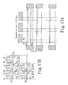
- FIG. 17A is a schematic view of the arrangement of the gate lines and the data lines of the display panel of the fourth embodiment according to the present invention, which shows the state of the gate drivers respectively installed on the left side and the right side of the display panel;
- FIG. 17B is an enlarged schematic sectional view taken from FIG. 17A , which shows the arrangement of the gate lines and the data lines and the state of the gate and the source, which are connected to the gate lines and the data lines, of each thin film transistor;
- FIG. 18 is a wave form view of the signal used in the driving method of the display device of the fourth embodiment according to the present invention, which shows the variation of the wave form of the signal of the gate lines and the data lines from the gate drivers and the source drivers at different frame interval time;
- FIG. 19 is a wave form view of the signal used in another driving method of the display device of the fourth embodiment according to the present invention, which shows the variation of the wave form of the signal of the gate lines and the data lines from the gate drivers and the source drivers at different frame interval time;
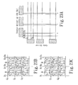
- FIG. 20A is a schematic view showing the arrangement of the gate lines and the data lines of the display panel of the fifth embodiment according to the present invention.
- FIG. 20B is an enlarged schematic sectional view taken from FIG. 20A , which shows the arrangement of the gate lines and the data lines and the state of the gate and the source, which are connected to the gate lines and the data lines, of each thin film transistor;
- FIG. 20C is an enlarged schematic sectional view taken from FIG. 20A , which shows there is a space between the neighboring gate lines to prevent them from short circuit;
- FIG. 21A is a schematic view of the arrangement of the gate lines and the data lines of the display panel of the fifth embodiment according to the present invention, which shows the state of the gate drivers respectively installed on the left side and the right side of the display panel;
- FIG. 21B is an enlarged schematic sectional view taken from FIG. 21A , which shows the arrangement of the gate lines and the data lines and the state of the gate and the source, which are connected to the gate lines and the data lines, of each thin film transistor;
- FIG. 22 is a wave form view of the signal used in the driving method of the display device of the fifth embodiment according to the present invention, which shows the variation of the wave form of the signal of the gate lines and the data lines from the gate drivers and the source drivers at different frame interval time;
- FIG. 23A is a schematic view showing the arrangement of the gate lines and the data lines of the display panel of the sixth embodiment according to the present invention.
- FIG. 23B is an enlarged schematic sectional view taken from FIG. 22A , which shows the arrangement of the gate lines and the data lines and the state of the gate and the source, which are connected to the gate lines and the data lines, of each thin film transistor;
- FIG. 23C is an enlarged schematic sectional view taken from FIG. 22A , which shows another arrangement of the gate lines and the data lines and the state of the gate and the source, which are connected to the gate lines and the data lines, of each thin film transistor;
- FIG. 23D is an enlarged schematic sectional view taken from FIG. 23A , which shows there is a space between the neighboring data lines for preventing them from short circuit;
- FIG. 24A is a schematic view of the arrangement of the gate lines and the data lines of the display panel of the sixth embodiment according to the present invention, which shows the state of the source drivers respectively installed on the upper side and the lower side of the display panel;
- FIG. 24B is an enlarged schematic sectional view taken from FIG. 24A , which shows the arrangement of the gate lines and the data lines and the state of the gate and the source, which are connected to the gate lines and the data lines, of each thin film transistor;
- FIG. 25A is a schematic view of the arrangement of the gate lines and the data lines of the display panel of the sixth embodiment according to the present invention, which shows the state of each pair of data lines connected to a source driver which is connected to the electronic switch;
- FIG. 25B is an enlarged schematic sectional view taken from FIG. 25A , which shows the arrangement of the gate lines and the data lines and the state of the gate and the source, which are connected to the gate lines and the data lines, of each thin film transistor;
- FIG. 26 is a wave form view of the signal used in the driving method of the display device of the sixth embodiment according to the present invention, which shows the variation of the wave form of the signal of the gate lines and the data lines from the gate driver and the source driver at different frame interval time;
- the design of driving IC for the liquid crystal display panel would consider these characteristics.
- the display is driven by voltage V 5 and reaches the expected brightness of some code in the time t 0
- the variation of its brightness is shown as the curve with mark 25 and is recorded.
- the liquid crystal display is driven by different voltage V 1 , V 2 , V 3 , and V 4 and reaches each expected brightness in the time t 0 .
- the brightness variation of each image versus time is shown as the curves of 21 , 22 , 23 , and 24 .
- the higher the voltage value the faster the brightness variation.
- the number of the measurement for the voltage versus brightness variation is decided by the requirement.
- the data of the voltage versus brightness variation for the display panel can be made into a lookup table to be a base for setting the brightness of the panel driven.
- the gray level value of the display When the gray level value of the display is zero, it means that the frame is completely black.
- the gray level of the display is under some value, for example code 5 ⁇ 10 , it can be regarded as black image. But the black image or the voltage, which make frame black, is still expressed by code 0 in the following statement.
- the driving device includes a group of thin film transistors Q with matrix array, which consists of N rows and M columns of thin film transistors, wherein, each thin film transistor Q can drive one pixel, so there are N ⁇ M pixels (shown by rectangle with dotted line) can be driven.
- the first gate line G 1 is connected with the gates of all the thin film transistors Q of the first row
- the second gate line G 2 is connected with the gates of all the thin film transistors Q of the second row, and so are the others. Therefore, there are N gate lines connected to gate driver and they are insulated with each other.
- the first and the second data lines D 1 , D 1′ of the first group of data lines are respectively connected with the sources of all the thin film transistors Q of the odd and the even rows of the first column.
- the first and the second data lines D 2 , D 2′ of the second group of data lines are respectively connected with the sources of all the thin film transistors Q of the odd and the even rows of the second column and so are the others. Therefore, in total there are M groups of data lines connected to the data drivers and they are insulated with each other.
- a space is given between the neighboring data lines, of which arrangement is shown as FIG. 5C .
- the source drivers connected with the data lines are installed on the same side of the display panel. If the scanning frequency is 60 Hz and there are two gate lines being turned on at the same time, the scanning time can be further decreased.
- the source drivers are respectively arranged on the upper and the lower sides of the liquid crystal display, and the first and the second data line of each group of data lines are respectively connected with the source drivers of the upper and the lower sides of the liquid crystal display, wherein, the scanning frequency of the source drivers is kept at 60 Hz.
- the first data line and the neighboring second line of each group of data lines are connected with the same source driver, and the data transfer is switched by an electronic switch S of which scanning frequency is a multiple of 60 Hz, such as 120 Hz, 180 Hz . . . etc.
- the form of the gate driver can be a chip on glass or an integrated gate driver circuit on glass.
- the driving method of the present invention executed by the said device, when time enters the present frame interval I from the preceding frame interval, the expected brightness is code 32 and V LC is the driving voltage pulse, the voltage wave form has positive and negative phases due to the driving voltage of the liquid crystal being alternating current.
- the voltage value will be expressed with code in the following statement.
- curve (a) represents the brightness variation of the pixel after being driven. If there are 2(m+n), i.e.
- N 2(m+n)
- the period of the voltage of displaying the present frame interval data for the thin film transistor connected with the first gate line is set as the displaying brightness period t 1
- the period of the voltage of displaying black image received by the thin film transistor connected with the first gate line is set as displaying black image period t 2 .
- the first gate line G 1 and the 2n th gate line G 2n are simultaneously turned on, and the voltage code 32 of displaying the present frame data is given to the thin film transistor connected to the first gate line G 1 , the voltage code 0 of the preceding frame is given to the thin film transistor Q connected to the 2n th gate line G 2n , in other words, the gate driver gives the control voltage pulse to the first gate line G 1 and the 2n th gate line G 2n at the same time, the source driver gives the voltage code 32 of displaying the present frame data to the thin film transistor Q connected to the first gate line G 1 , the voltage code 0 of the preceding frame data is given to the thin film transistor Q connected to the 2n th gate line G 2n .
- the second and the 2n+1 th gate lines, the third and the 2n+2 th gate lines . . . the 2m ⁇ 1 th and the 2(n+m) ⁇ 2 th gate lines are turned on in order, and the voltage code 32 of displaying the present frame data is given to the thin film transistors Q connected to the second to the 2m ⁇ 1 th gate lines, the voltage code 0 of the preceding frame data is given to the thin film transistors Q connected to the 2n+1 th to the 2(m+n) ⁇ 2 th gate lines.
- the 2m th and the first gate lines G 2m , G 1 are simultaneously turned on, and the voltage code 32 of displaying the present frame data is given to the thin film transistor Q connected to the 2m th gate line G 2m , the voltage code 0 of displaying black image is given to the thin film transistor Q connected to the first gate line G 1 .
- the 2(m+n) th (the last) and the 2n ⁇ 1 th gate lines are turned on in order, and the voltage code 32 of displaying the present frame data is given to the thin film transistors Q connected to the 2m+1 to the 2(m+n) th (the last) gate lines, the voltage of displaying black image is given to the thin film transistors connected to the second to the 2n ⁇ 1 th gate lines.
- the ratio of the number of the gate lines which were scanned in the displaying brightness period to the number of the total gate lines is P and the period of the frame interval of the liquid crystal display is T, then the duration of the displaying brightness is PT and the duration of the keeping brightness is (1 ⁇ P)T.
- the ratio P can be adjusted according the characteristic of the display panel.
- the second embodiment of the driving device for quickly changing the gray level of the liquid crystal display includes a group of thin film transistors with matrix array, which consist of 2N rows and M columns of thin film transistors Q, wherein, each thin film transistor Q can drive one pixel so that there are 2N ⁇ M of pixels (shown by the rectangle with dotted line) can be driven in total.
- the first gate line G 1 is connected with the gates of all the thin film transistors Q of the first and the second rows
- the second gate line G 2 is connected with the gates of all the thin film transistors Q of the third and the fourth rows, and so are the others. Therefore, total N gate lines connected to the gate drivers and insulated with each other.
- the first and the second data lines D 1 , D 1′ of the first group of data lines are respectively connected with the sources of all the thin film transistors of the odd rows and the even rows of the first column
- the first and the second data lines D 2 , D 2′ of the second group of data lines are respectively connected with the sources of all the thin film transistors of the odd and the even rows of the second column and so are the others. Therefore, in total there are M groups of data lines connected to the data drivers and they are insulated with each other.
- the second data line D 1′ of the first group of data lines and the first data line D 2 of the second group of data lines there is a space between the neighboring data lines, of which arrangement is shown in FIG. 9C .
- the aspect ratio of the liquid crystal display can be increased.
- the source drivers connected with the data lines are installed on the same side of the display panel. If the scanning frequency is 60 Hz and two gate lines are simultaneously turned on, the scanning time can be further reduced.
- the arrangement of the source drivers is shown as FIGS. 10A and 10B .
- the first and the second data lines of each group of data lines are respectively connected with the source drivers installed on the upper and the lower sides of the liquid crystal display, wherein the scanning frequency of the source drivers is kept at 60 Hz.
- the first data line and the second line of each group of data lines are connected with the same source driver, and the data transfer is switched by an electronic switch, of which scanning frequency is a multiple of 60 Hz, such as 120 Hz, 180 Hz . . . etc.
- the form of the gate driver can be a chip on glass or an integrated gate driver circuit on glass.
- the driving method of the present invention executed by the said device, when time enters the frame interval 1 , the expected brightness is code 32 and V LC the driving voltage pulse.
- the value of the driving voltage pulse will be expressed with code in the following statement.
- curve (a) represents the brightness variation of the pixel after being driven.
- the period of the voltage of displaying the present frame data for the thin film transistor connected with the first gate line is set as the displaying brightness period t 1
- the period of the voltage of displaying black image received by the thin film transistor connected with the first gate line is set as the displaying black image period t 2 .
- the first and the n th gate lines G 1 , G n are orderly turned on in a synchronous control time.
- the voltage of displaying the present frame data and the voltage of displaying black image are respectively given to the thin film transistors Q connected with the first and the n th gate lines.
- the voltage code 32 of displaying the present frame data is given to the thin film transistors Q connected with the second to m th gate lines
- the voltage code 0 of displaying black image is given to the thin film transistors Q connected with the n+1 th to m+n ⁇ 1 th gate lines.
- the m+1 th and the first gate lines G m+1 , G 1 are orderly turned on in a synchronous control time.
- the voltage code 32 of displaying the present frame data and the voltage code 0 of displaying black image are respectively given to the thin film transistors Q connected with the m+1 th and the first gate lines G m+1 , G 1 .
- the m+2 th and the second gate lines, the m+3 th and the third gate lines . . . and the m+n th (i.e. the last) and the n ⁇ 1 th gate lines G m+n , G n ⁇ 1 are orderly and synchronously turned on.
- the voltage of displaying the present frame data is given to the thin film transistors Q connected with the m+n th to m+n th (i.e. the last) gate lines, and the voltage of displaying black image is given to the thin film transistors Q connected with the second to the n ⁇ 1 th gate lines.
- the ratio of the number of the gate lines scanned in the displaying brightness period t 1 to the number of the total gate lines is P and the period of the frame interval of the liquid crystal display is T, then the duration of the displaying brightness is PT and the duration of the keeping brightness is (1 ⁇ P)T.
- the ratio P can be adjusted according the characteristic of the display panel.
- the third embodiment of the driving device for quickly changing the gray level of the liquid crystal display according to the present invention includes a group of thin film transistors with matrix array, which consists of N rows and 2M columns of thin film transistors Q, wherein each thin film transistor can drive one pixel, so there are in total N ⁇ 2M of pixels (shown by the rectangle of dotted line).
- the first and the second gate lines G 1 , G 1′ of the first group of the gate lines are respectively connected with the gates of all the thin film transistors of the odd columns and the even columns of the first row
- the first and the second gate lines G 2 , G 2′ of the second group of gate lines are respectively connected with the gates of all the transistors Q of the odd columns and the even columns of the second row . . .
- the first and the second gate lines of the N th group of gate lines are respectively connected with the gates of all the thin film transistors of the odd columns and the even columns of the N th row, therefore, there are in total N groups of gate lines connected to the gate drivers and insulated with each other.
- the first data line D 1 is connected with the sources of all the thin film transistors Q of the first and the second columns
- the second data line D 2 is connected with the sources of all the thin film transistors Q of the third and the fourth columns . . .
- the M th data line is connected with the sources of all the thin film transistors Q of the 2M ⁇ 1 th and the 2M th columns. Therefore, there are in total M data lines connected with the source drivers and insulated with each other.
- the first and the second gate lines G 1 , G 1′ of the first group of gate lines there is a space between the neighboring gate lines, of which arrangement is shown as FIG. 13C .
- the gate drivers connected with the gate lines are installed on the same side of the display panel.
- the first and the second gate lines of each group of gate lines are respectively given data by two groups of gate drivers, and the two groups of gate drivers are respectively installed on the left side and the right side of the liquid crystal display.
- the form of the gate driver can be a chip on glass, or an integrated gate driver circuit on glass.
- the driving method of the present invention executed by the said device, when time enters the frame interval 1 , the expected brightness is code 32 and V LC is the driving voltage pulse. To prevent the driving voltage pulse from confusing with the alternating voltage for driving liquid crystal, the value of the driving voltage pulse is expressed with code.
- curve (a) expresses the brightness variation of the pixel after being driven.
- the period of the voltage of displaying the present frame data received by the thin film transistor connected with the first gate line of the first group of gate lines is set as the displaying brightness period t 1
- the period of the voltage displaying black image received by the thin film transistor connected to the first gate line of the first group of gate lines is set as the displaying black image period t 2 .
- the first and the second gate line G 1 , G 1′ of the first group of gate lines are orderly turned on in a time of one synchronous control signal.
- the voltage code 32 of displaying the present frame interval data is given to the thin film transistors Q connected with the first and the second gate lines of the first group of gate lines, and the first and the second gate lines G n , G n′ of the n th group of gate lines are orderly turned on by the synchronous control signal.
- the voltage code 0 of displaying black image is given to the thin film transistors Q connected with the first and the second gate lines G n , G n′ of the n th group of gate lines.
- the first and the second gate lines of the second group of gate lines, the first and the second gate lines of the n+1 th gate lines . . . the first and the second gate lines of the m+n th group of gate lines, the first and the second gate line G m+1 , G m+1′ of the m+1 th gate lines are orderly and synchronously turned on.
- the voltage code 32 of displaying the present frame interval data is given to the thin film transistors Q connected with the second to the m+1 th groups of gate lines.
- the voltage code 0 of displaying black image is given to the thin film transistors Q connected with the n+1 th to the m+n th group of gate lines.
- the first and the second gate lines of the first group of gate lines are orderly turned on.
- the voltage code 0 of displaying black image interval is given to the thin film transistors connected with the said gate lines.
- the first and the second gate lines of the m+2 th group of gate lines are orderly turned on by the synchronous control signal.
- the voltage code 32 of displaying the present frame interval data is given to the thin film transistors Q connected with the said gate lines.
- the voltage code 0 of displaying black image is given to the thin film transistors connected with the second to the n ⁇ 1 th gate lines.
- the voltage code 32 of displaying the present frame interval data is given to the thin film transistors Q connected with the m+3 th to the m+n th gate lines.
- the ratio of the number of the gate lines scanned in the displaying brightness period t 1 to the number of the total gate lines is P and the period of the frame interval of the liquid crystal display is T, then the displaying brightness duration is PT and the keeping brightness duration is (1 ⁇ P)T.
- the ratio P can be adjusted according to the characteristic of the display panel.
- the fourth embodiment of the driving device for quickly changing the gray level of the liquid crystal display includes a group of thin film transistors Q with matrix array, which consists of N rows and M columns of thin film transistors Q, wherein each thin film transistor Q can drive one pixel, so total 2N ⁇ M of pixels (shown by the rectangle with dotted line) can be driven.
- the first gate line G 1 of the first group of gate lines is connected with the gates of all the thin film transistors Q of the first row
- the second gate line G 1′ of the first group of gate lines is connected with the gates of all the thin film transistors Q of the second row . . .
- the second gate line of the N th group of gate lines is connected with the gates of all the thin film transistors Q of the 2N th row, therefore, there are in total N groups of gate lines connected to gate drivers and insulated with each other.
- the first and the second data lines D 1 , D 2 are respectively connected with the sources of all the thin film transistors Q of the odd and the even rows of the first column
- the second and the third data lines D 3 , D 4 are respectively connected with the sources of all the thin film transistors Q of the odd and the even rows of the second column . . .
- the M th and the M+1 th data lines are respectively connected with the sources of all the thin film transistors Q of the odd and the even rows of the M th column, therefore there are in total M+1 data lines connected to the source drivers and insulated with each other.
- FIG. 16C which is the other form of the fourth embodiment. It also consists of 2N rows and M columns of thin film transistors Q, wherein each thin film transistor. Q can drive one pixel, so total 2N ⁇ M of pixels (shown by rectangle with dotted line) can be driven.
- the first gate line G 1 of the first group of gate lines is connected with the gates of all the thin film transistors Q of the first row
- the second gate line G 2 of the first group of gate lines is connected with the gates of all the thin film transistors Q of the second row . . .
- the first data line D 1 is connected with the sources of all the thin film transistors Q of the first column
- the second data line D 2 is connected with the sources of all the thin film transistors Q of the second column . . .
- the M th data line is connected with the sources of all the thin film transistors Q of the M th column, therefore, there are in total M data lines connected to the source drivers and insulated with each other.
- the gate drivers connected with the gate lines are installed on the same side of the display panel.
- the first gate line and the second gate line of each group of gate lines are respectively given data by two groups of gate drivers, and the said two groups of gate drivers are respectively installed on the left and the right sides of the liquid crystal display.
- the form of the gate driver can be a chip on glass, or an integrated gate driver circuit on glass.
- the expected brightness is code 32 and the V LC is the driving voltage pulse.
- the value of the driving voltage is expressed with code in the following statement.
- curve (a) expresses the brightness variation of the pixel after being driven.
- the period of the voltage of displaying the present frame interval data received by the thin film transistors connected with the first gate line of the first group of gate lines is set as the displaying brightness period t 1
- the period of voltage of displaying black image received by the thin film transistors connected with the first gate line of the first groups of gate lines is set as the displaying black image period t 2 .
- the first and the second gate lines G 1 , G 1′ of the first group of gate lines are orderly turned on in a time of one synchronous control signal.
- the voltage code 32 of displaying the present frame interval data is given to the thin film transistors Q connected with the first and the second gate lines G 1 , G 1′ of the first group of gate lines.
- the first and the second gate lines G n , G n′ of the n th group of gate lines are orderly turned on by the synchronous control signal.
- the voltage code 0 of displaying black image is given to the thin film transistor Q connected with the said gate lines.
- the first and the second gate lines of the second group of gate lines, the first and the second gate lines of the n+1 th group of gate lines . . . the first and the second gate lines of the m+n ⁇ 1 th group of gate lines and the first and the second gate lines G m+1 , G m+1′ of the m+1 th group of gate lines are orderly and simultaneously turned on in a time of synchronous control signal.
- the voltage code 32 of displaying the present frame interval data is given to the thin film transistors Q connected with the second to the m+1 th groups of gate lines.
- the voltage code 0 of displaying black image is given to the thin film transistors Q connected with the n+1 th to the m+n ⁇ 1 th groups of gate lines.
- the first and the second gate lines G 1 , G 1′ of the first group of gate lines are orderly turned on in a time of one synchronous control signal.
- the voltage code 0 of displaying black image is given to the thin film transistors connected with the said gate lines.
- the first and the second gate lines of the m+2 th group of gate lines are orderly turned on by the synchronous control signal.
- the voltage code 32 of displaying the present frame interval data is given to the thin film transistors connected with the said gate lines.
- the voltage code 32 of displaying the present frame interval data is given to the thin film transistors Q connected with the m+3 th to the last gate lines.
- the voltage code 0 of displaying black image is given to the transistors Q connected with the second to the n ⁇ 1 th group of gate lines.
- FIG. 19 it shows the second driving method of the present invention.
- the expected brightness is code 32 and V LC is the driving voltage pulse.
- the voltage value is expressed with code in the following statement to prevent the driving voltage from confusing with the alternating voltage for driving the liquid crystal.
- curve (a) expresses the brightness variation of the pixel after being driven.
- the period of the voltage of displaying the present frame interval data received by the thin film transistors connected with the first gate line of the first group of gate lines is set as the displaying brightness period t 1
- the period of the voltage of displaying black image received by the thin film transistors connected with the first gate line of the first group of gate lines is set as the displaying black image period t 2 .
- the first gate line G 1 of the first group of gate lines and the first gate line G n of the n th group of gate lines are orderly turned on in a time of one synchronous control signal.
- the voltage code 32 of displaying the present frame interval data and the voltage code 0 of displaying black image are respectively given to the thin film transistors Q connected with the said gate lines.
- the voltage code 32 of displaying the present frame interval data is given to the thin film transistors Q connected with the first to the m th groups of gate lines.
- the voltage code 0 of displaying black image is given to the thin film transistors Q connected with the n+1th to the m+n ⁇ 1th groups of gate lines.
- the first gate line G 1 of the first group of gate lines and the first gate line of the m+2 th group of gate lines are orderly turned on in a time of one synchronous control signal.
- the voltage code 0 of displaying black image and the voltage code 32 of displaying the present frame interval data are respectively given to the thin film transistors Q connected with the said gate lines.
- the voltage code 32 of displaying the present frame interval data is given to the thin film transistors Q connected with the m+1 th group to the last gate line G (m+n)′ .
- the voltage code 0 of displaying black image is given to the thin film transistors Q connected with the second group of gate lines to the n ⁇ 1 th group of gate lines.
- the ratio of the number of the gate lines scanned in the displaying brightness period t 1 to the number of the total gate lines is P and the period of the frame interval of the liquid crystal display is T, then the displaying brightness duration is PT and the keeping brightness duration is (1 ⁇ P)T.
- the ratio P can be adjusted according to the characteristic of the display panel.
- the fifth embodiment of the driving device for quickly changing the gray level of the liquid crystal display according to the present invention includes a group of thin film transistors Q with matrix array, which consists of N rows and 2M columns of thin film transistors Q.
- One pixel is driven by two neighboring thin film transistors Q, therefore total.
- N ⁇ M of pixels shown by rectangle with dotted line
- the first and the second gate lines G 1 , G 1′ of the first group of gate lines are respectively connected with the gates of all the thin film transistors Q of the odd and the even columns of the first row.
- the first and the second gate lines G 2 , G 2′ of the second group of gate lines are respectively connected with the gates of all the thin film transistors Q of the odd and the even columns of the second row . . . and the first and the second gate lines of the N th group of gate lines are respectively connected with the gates of all the thin film transistors Q of the odd and the even columns of the N th row. Therefore, there are in total N groups of gate lines connected to the gate drivers and insulated with each other.
- the first data line D 1 is connected with the sources of all the thin film transistors Q of the first column.
- the second data line D 2 is connected with the sources of all the thin film transistors Q of the second column . . . and the 2M th data line is connected with the sources of all the thin film transistors Q of the 2M th column. Therefore, there are in total 2M data lines connected to the source drivers and insulated with each other.
- the neighboring gate lines from short circuit, for example, the first gate line G 1 and the second gate line G 1′ of the first group of gate lines, there is a space between the two neighboring gate lines, of which arrangement is shown as FIG. 20C .
- the gate drivers connected with the gate lines are installed on the same side of the display panel.
- the first gate line and the second gate line of each group of gate lines are respectively given data by two groups of gate drivers, and the said two groups of gate drivers are respectively installed on the left and the right sides of the liquid crystal display.
- the form of the gate driver can be a chip on glass or an integrated gate driver circuit on glass.
- the driving method of the present invention can be executed by the device stated above.
- the expected brightness is code 32 and V LC is the driving voltage pulse.
- the value of the driving voltage pulse is expressed with code in the following statement to prevent the driving voltage from confusing the alternating voltage for driving liquid crystal.
- curve (a) expresses the brightness variation of the pixel after being driven.
- the period of the voltage of displaying the present frame interval data received by the thin film transistors connected with the first gate line of the first group of gate lines is set as the displaying brightness period t 1
- the period of the voltage of displaying black image received by the thin film transistors connected with the second gate line of the first group of gate lines is set as the displaying black image period t 2 .
- the first gate line G 1 of the first group of gate lines and the second gate line G n′ of the n th group of gate lines are orderly turned on in a time of one synchronous control signal.
- the voltage code 32 of displaying the present frame interval data and the voltage code 0 of displaying black image are respectively given to the thin film transistors Q connected with the said gate lines.
- the voltage code 32 of displaying the present frame interval data is given to the thin film transistors Q connected with the first gate line of the second group to the m+1 th group of gate lines.
- the voltage code° of displaying black image is given to the thin film transistors Q connected with the second gate line of the n+1 th group to the m+n ⁇ 1 th group of gate lines.
- the second gate line G 1′ of the first group of gate lines and the first gate line of the m+2 th group of gate lines are orderly turned on in a time of one synchronous control signal.
- the voltage code 0 of displaying black image and the voltage code 32 of displaying the present frame interval data are respectively given to the thin film transistors Q connected with the said gate lines.
- the voltage code 0 of displaying black image is given to the thin film transistors Q connected with the second gate line of the second group to the n ⁇ 1 th group of gate lines.
- the voltage code 32 of displaying the present frame interval data is given to the thin film transistors Q connected with the first gate lines of the m+3 th group to the m+n th group of gate lines.
- the ratio of the number of the gate lines scanned in the displaying brightness period t 1 to the number of the total gate lines is P and the frame interval period of the liquid crystal display is T, then the displaying brightness duration is PT and the keeping brightness duration is (1 ⁇ P)T.
- the ratio P can be adjusted according to the characteristic of the display panel.
- the sixth embodiment of the driving device for quickly changing the gray level of the liquid crystal display includes a group of thin film transistors Q with matrix array, which consists of N rows and 2M columns of thin film transistors Q.
- One pixel is driven by two neighboring thin film transistors so that total N ⁇ M of pixels (shown by the rectangle with dotted line) can be driven.
- the first and the second gate lines G 1 , G 2 are respectively connected with the gates of all the thin film transistors Q of the odd column and the even column of the first row.
- the second and the third gate lines G 2 , G 3 are respectively connected with gates of all the thin film transistors Q of the odd column and the even column of the second row . . . and the N th and the N+1 th gate lines are respectively connected with the gates of all the thin film transistors Q of the odd column and the even column of the N th row. Therefore, there are in total N gate lines connected to the gate drivers and insulated with each other.
- the first data line D 1 of the first group of data lines is connected with the sources of all the thin film transistors Q of the first column.
- the second data line D 1′ of the first group of data lines is connected with the sources of all the thin film transistors Q of the second column . . . and the second data line of the M th group of data lines is connected with the sources of all the thin film transistors Q of the 2M th column. Therefore, there are in total M groups of data lines connected to the source drivers and insulated with each other.
- a row of thin film transistors Q can be additionally installed above the first row of thin film transistors Q in the present embodiment.
- Each thin film transistor Q can control a pixel.
- the gates of the said row of thin film transistors Q are connected with the first gate line and their sources are connected with the second data line of each group of data lines.
- the neighboring data lines from short circuit, for example, the second data line D 1′ of the first group of data lines and the first data line D 2 of the second group of data lines, there is a space between two neighboring data lines of which arrangement is shown as FIG. 23D .
- the source drivers connected with the data lines are installed on the same side. If the scanning frequency is 60 Hz and two gate lines are simultaneously turned on, the scanning time can be further decreased.
- the source drivers can be arranged as shown in FIGS. 24A and 24B .
- the first data line of each group of data lines and the second data line of each group of data lines are respectively connected with the source drivers installed on the upper side and the lower side of the liquid crystal display.
- the scanning frequency of the source drivers is kept at 60 Hz.
- FIGS. 25A and 25B the first data line of each group of data lines and the second data line of each group of data lines, which are neighboring, are connected with the same source driver.
- the data transfer is switched by an electronic switch. Its scanning frequency is a multiple of that of the said source driver, for examples, 120 Hz, 180 Hz . . . etc.
- the form of the gate driver can be a chip on glass, or an integrated gate driver circuit on glass.
- the driving method of the present invention is executed with the device stated above.
- the expected brightness is code 32 and V LC is the driving voltage pulse.
- the value of the driving voltage is expressed with code in the following statement to prevent the driving voltage from confusing the alternating voltage for driving liquid crystal.
- curve (a) expresses the brightness variation of the pixel after being driven.
- the period of the voltage of displaying the present frame interval data received by the thin film transistor connected with the first gate line is set as the displaying brightness period t 1 and the period of the voltage of displaying black image received by the thin film transistors connected with the first gate line is set as the displaying black image period t 2 .
- the first and the n+1 th gate lines G 1 , G n+1 are orderly turned on in a time of one synchronous control signal.
- the voltage code 32 of displaying the present frame interval data and the voltage code 0 of displaying black image are respectively given to the thin film transistors Q connected with the said gate lines.
- the second and the n+2 th gate lines, the third and the n+3 th gate lines . . . and the m+n ⁇ 1 th and the m th gate lines are orderly and synchronously turned on in the time of synchronous control signal.
- the voltage code 32 of displaying the present frame interval data is given to the thin film transistors connected with the second to the m th gate lines.
- the voltage code 0 of displaying black image is given to the thin film transistors Q connected with the n+2 th to the m+n ⁇ 1 th gate lines.
- the voltage code 32 of displaying the present frame interval data and the voltage code 0 of displaying black image are respectively given to the thin film transistors Q connected with the said gate lines.
- the second and the m+2 th gate lines, the third and the m+3 th gate lines . . . and the m+n th (i.e. the last) and the n th gate lines are orderly turned on.
- the voltage code 32 of displaying the present frame interval data is given to the thin film transistors Q connected with the m+2 th to the m+n th (the last) gate lines.
- the voltage code 0 of displaying black image is given to the thin film transistors Q connected with the second to the n th gate lines.
- the displaying brightness duration is PT and the keeping brightness duration is (1 ⁇ p)T.
- the ratio P can be adjusted according to the characteristic of the display panel.
- the present invention can quickly drive the liquid crystal display and quickly change the display value of the gray level of the liquid crystal display by the division of the time (frame interval time) and space (gate lines) and the application of the voltage of displaying the present frame brightness and the voltage of displaying black image in the steps stated above.
- the driving method according to the present invention can suit for various picture treatments of liquid crystal display, organic light emitting diode (OLED) display or plasma display panel (PDP).
- OLED organic light emitting diode
- PDP plasma display panel
- the present invention has the following advantages:
- the present invention indeed can accomplish its expected object of providing a driving device for quickly changing the gray level of the liquid crystal display and its driving method.
- the present invention has the advantage of the image display in the traditional CRT display and can improve the drawback of the image display of the liquid crystal display. Therefore the present invention has very high utilization value in industry, so it is brought forward claiming patent right.
Abstract
Description
- (1) The black color data or the black image is inserted in the continuous image frame: if F1, F2, F3, and F4 are the frames of the series of continuous image, the black images B1, B2, and B3 can be inserted between the continuous image frames with a multiple scanning frequency. After the expected brightness of the display is reached, it can be removed by the black image data. This method can simulate the display of CRT.
- (2) The black image signal is inserted in the back light source to make the back light source flicker: The brightness of every frame is originally provided by the light source at the back of the display panel. If L1, L2, L3, and L4 are the continuous back light source and the black image signals are inserted between the back light sources, the light source can be forced to close and produce the black image B1, B2, and B3. This method can also get the effect of simulating the display of CRT and remove the afterimage phenomenon.
- 1. The liquid crystal display driven by the driving method of quickly changing the gray level according to the present invention can improve the phenomenon of the afterimage in the traditional liquid crystal display and keep the advantages in the traditional CRT display, hence it possesses good effect in visual feeling.
- 2. Besides dividing the scanning area of the display panel, the ratio of each scanning area can be adjusted and kept according to the characteristic of the panel. The present invention can suit for various display panels and possesses very high utilization value in industry.
- 3. The present invention can avoid the electromagnetic interference and the high equipment cost due to the technique of switching the back light source in the prior art by the application of the driving voltage for displaying black image.
Claims (18)
Priority Applications (1)
| Application Number | Priority Date | Filing Date | Title |
|---|---|---|---|
| US12/140,674 US8390551B2 (en) | 2004-08-31 | 2008-06-17 | Driving device for quickly changing the gray level of the liquid crystal display and its driving method |
Applications Claiming Priority (2)
| Application Number | Priority Date | Filing Date | Title |
|---|---|---|---|
| US10/929,564 US20060044241A1 (en) | 2004-08-31 | 2004-08-31 | Driving device for quickly changing the gray level of the liquid crystal display and its driving method |
| US12/140,674 US8390551B2 (en) | 2004-08-31 | 2008-06-17 | Driving device for quickly changing the gray level of the liquid crystal display and its driving method |
Related Parent Applications (1)
| Application Number | Title | Priority Date | Filing Date |
|---|---|---|---|
| US10/929,564 Division US20060044241A1 (en) | 2004-08-31 | 2004-08-31 | Driving device for quickly changing the gray level of the liquid crystal display and its driving method |
Publications (2)
| Publication Number | Publication Date |
|---|---|
| US20100265270A1 US20100265270A1 (en) | 2010-10-21 |
| US8390551B2 true US8390551B2 (en) | 2013-03-05 |
Family
ID=35942359
Family Applications (3)
| Application Number | Title | Priority Date | Filing Date |
|---|---|---|---|
| US10/929,564 Abandoned US20060044241A1 (en) | 2004-08-31 | 2004-08-31 | Driving device for quickly changing the gray level of the liquid crystal display and its driving method |
| US12/122,084 Expired - Fee Related US7636099B2 (en) | 2004-08-31 | 2008-05-16 | Driving device for quickly changing the gray level of the liquid crystal display and its driving method |
| US12/140,674 Active 2025-09-12 US8390551B2 (en) | 2004-08-31 | 2008-06-17 | Driving device for quickly changing the gray level of the liquid crystal display and its driving method |
Family Applications Before (2)
| Application Number | Title | Priority Date | Filing Date |
|---|---|---|---|
| US10/929,564 Abandoned US20060044241A1 (en) | 2004-08-31 | 2004-08-31 | Driving device for quickly changing the gray level of the liquid crystal display and its driving method |
| US12/122,084 Expired - Fee Related US7636099B2 (en) | 2004-08-31 | 2008-05-16 | Driving device for quickly changing the gray level of the liquid crystal display and its driving method |
Country Status (1)
| Country | Link |
|---|---|
| US (3) | US20060044241A1 (en) |
Families Citing this family (21)
| Publication number | Priority date | Publication date | Assignee | Title |
|---|---|---|---|---|
| US20060044241A1 (en) * | 2004-08-31 | 2006-03-02 | Vast View Technology Inc. | Driving device for quickly changing the gray level of the liquid crystal display and its driving method |
| JP4437110B2 (en) * | 2004-11-17 | 2010-03-24 | 三星モバイルディスプレイ株式會社 | Organic light emitting display device, driving method of organic light emitting display device, and driving method of pixel circuit |
| TWI303407B (en) * | 2004-12-24 | 2008-11-21 | Innolux Display Corp | Driving circuit of display and method of driving the circuit |
| TWI354970B (en) * | 2005-12-26 | 2011-12-21 | Lg Display Co Ltd | Display and driving method thereof |
| US8519928B2 (en) * | 2006-06-22 | 2013-08-27 | Entropic Communications, Inc. | Method and system for frame insertion in a digital display system |
| US7852446B2 (en) * | 2006-09-18 | 2010-12-14 | Samsung Electronics Co., Ltd. | Liquid crystal display and method of driving the same |
| JP5177139B2 (en) * | 2007-11-15 | 2013-04-03 | パナソニック株式会社 | Plasma display apparatus and driving method of plasma display panel |
| US8502749B2 (en) * | 2007-11-15 | 2013-08-06 | Panasonic Corporation | Plasma display apparatus and driving method for plasma display apparatus |
| WO2009084331A1 (en) * | 2007-12-27 | 2009-07-09 | Sharp Kabushiki Kaisha | Liquid crystal display, liquid crystal display driving method, and television receiver |
| CN101896961A (en) * | 2007-12-27 | 2010-11-24 | 夏普株式会社 | Liquid crystal display, liquid crystal display driving method, and television receiver |
| KR101570399B1 (en) * | 2009-03-02 | 2015-11-30 | 삼성디스플레이 주식회사 | Thin film transistor sustrate |
| JP5321269B2 (en) | 2009-06-16 | 2013-10-23 | ソニー株式会社 | Image display device, image display method, and program |
| US9111505B2 (en) * | 2011-09-20 | 2015-08-18 | Sharp Kabushiki Kaisha | Liquid crystal display device and drive method for liquid crystal panel |
| KR20150052997A (en) * | 2013-11-07 | 2015-05-15 | 삼성디스플레이 주식회사 | Organic light emitting display device and driving method thereof |
| TWI543142B (en) | 2014-09-12 | 2016-07-21 | 聯詠科技股份有限公司 | Source driver, operatoin method thereof and driving circuit using the same |
| CN105575344B (en) * | 2014-10-08 | 2018-10-02 | 联咏科技股份有限公司 | Source electrode driver, its operation method and its driving circuit |
| KR102266064B1 (en) * | 2014-10-15 | 2021-06-18 | 삼성디스플레이 주식회사 | Method of driving display panel, display panel driving apparatus and display apparatus having the display panel driving apparatus |
| CN105093757B (en) * | 2015-09-02 | 2018-03-30 | 京东方科技集团股份有限公司 | A kind of display panel and preparation method thereof, display device |
| KR102314647B1 (en) * | 2017-11-23 | 2021-10-19 | 삼성전자주식회사 | Method and device for processing an image and recording medium thereof |
| KR102552303B1 (en) * | 2018-06-21 | 2023-07-10 | 삼성디스플레이 주식회사 | Display device and driving mathod thereof |
| CN111048056A (en) * | 2019-12-19 | 2020-04-21 | 惠州Tcl移动通信有限公司 | Terminal equipment brightness adjusting method and system, storage medium and terminal equipment |
Citations (22)
| Publication number | Priority date | Publication date | Assignee | Title |
|---|---|---|---|---|
| US735566A (en) * | 1903-01-23 | 1903-08-04 | George W Mcgill | Wire-clip. |
| US4955698A (en) * | 1988-03-03 | 1990-09-11 | Robert Bosch Gmbh | Opto-electronic indicating matrix, and indicating device provided therewith |
| US5805128A (en) * | 1995-08-23 | 1998-09-08 | Samsung Electronics Co., Ltd. | Liquid crystal display device |
| US5949396A (en) * | 1996-12-28 | 1999-09-07 | Lg Semicon Co., Ltd. | Thin film transistor-liquid crystal display |
| US6057904A (en) * | 1996-10-29 | 2000-05-02 | Lg Electronics, Inc. | Insulating layer arrangements for liquid crystal display and fabricating method thereof |
| US6157056A (en) * | 1997-01-20 | 2000-12-05 | Kabushiki Kaisha Toshiba | Semiconductor memory device having a plurality of memory cell transistors arranged to constitute memory cell arrays |
| US6310594B1 (en) * | 1998-11-04 | 2001-10-30 | International Business Machines Corporation | Driving method and circuit for pixel multiplexing circuits |
| US20020003522A1 (en) * | 2000-07-07 | 2002-01-10 | Masahiro Baba | Display method for liquid crystal display device |
| US20030030609A1 (en) * | 2001-08-09 | 2003-02-13 | Hsin-Ta Lee | Display apparatus with a time domain multiplex driving circuit |
| US20030043104A1 (en) * | 2001-09-03 | 2003-03-06 | Samsung Electronics Co., Ltd. | Liquid crystal display apparatus |
| US20030090452A1 (en) * | 1999-03-16 | 2003-05-15 | Katsuhide Uchino | Liquid crystal display apparatus, its driving method and liquid crystal display system |
| US20030090614A1 (en) * | 2001-11-15 | 2003-05-15 | Hyung-Guel Kim | Liquid crystal display |
| US20030206149A1 (en) * | 2000-06-14 | 2003-11-06 | Junichi Yamashita | Display device and method for driving the same |
| US20040056331A1 (en) * | 2002-09-10 | 2004-03-25 | Au Optronics Corp. | Display panel with bypassing lines |
| US20040113879A1 (en) * | 2002-12-10 | 2004-06-17 | Hitachi, Ltd. | Liquid-crystal display device and method of driving liquid-crystal display device |
| US20050024353A1 (en) * | 2001-11-20 | 2005-02-03 | E Ink Corporation | Methods for driving electro-optic displays |
| US6903716B2 (en) * | 2002-03-07 | 2005-06-07 | Hitachi, Ltd. | Display device having improved drive circuit and method of driving same |
| US20060044241A1 (en) * | 2004-08-31 | 2006-03-02 | Vast View Technology Inc. | Driving device for quickly changing the gray level of the liquid crystal display and its driving method |
| US7038561B2 (en) * | 2004-09-20 | 2006-05-02 | Robert Esty | Do-it-yourself GFI outlet kit |
| US7038651B2 (en) * | 2002-03-20 | 2006-05-02 | Hitachi, Ltd. | Display device |
| US7420550B2 (en) * | 2004-08-31 | 2008-09-02 | Vast View Technology, Inc. | Liquid crystal display driving device of matrix structure type and its driving method |
| US7425937B2 (en) * | 2002-08-09 | 2008-09-16 | Semiconductor Energy Laboratory Co., Ltd. | Device and driving method thereof |
Family Cites Families (17)
| Publication number | Priority date | Publication date | Assignee | Title |
|---|---|---|---|---|
| JP3715996B2 (en) * | 1994-07-29 | 2005-11-16 | 株式会社日立製作所 | Liquid crystal display device |
| TW344043B (en) * | 1994-10-21 | 1998-11-01 | Hitachi Ltd | Liquid crystal display device with reduced frame portion surrounding display area |
| JP3267844B2 (en) * | 1994-11-09 | 2002-03-25 | シャープ株式会社 | Liquid crystal element and manufacturing method thereof |
| US5748164A (en) * | 1994-12-22 | 1998-05-05 | Displaytech, Inc. | Active matrix liquid crystal image generator |
| JPH1068931A (en) * | 1996-08-28 | 1998-03-10 | Sharp Corp | Active matrix type liquid crystal display device |
| EP1621923B8 (en) * | 1997-06-12 | 2010-03-24 | Sharp Kabushiki Kaisha | Vertically-aligned (VA) liquid crystal display device |
| CN1214282C (en) * | 1997-10-31 | 2005-08-10 | 精工爱普生株式会社 | Electro-optical device and electronic apparatus |
| JP3832125B2 (en) * | 1998-01-23 | 2006-10-11 | セイコーエプソン株式会社 | Electro-optical device and electronic apparatus |
| US6590553B1 (en) * | 1999-07-23 | 2003-07-08 | Nec Corporation | Liquid crystal display device and method for driving the same |
| TW493152B (en) * | 1999-12-24 | 2002-07-01 | Semiconductor Energy Lab | Electronic device |
| JP4550334B2 (en) * | 2001-09-27 | 2010-09-22 | 株式会社日立製作所 | Liquid crystal display device and method of manufacturing liquid crystal display device |
| JP3918496B2 (en) * | 2001-10-22 | 2007-05-23 | 株式会社日立製作所 | Liquid crystal display device and manufacturing method thereof |
| KR100890022B1 (en) * | 2002-07-19 | 2009-03-25 | 삼성전자주식회사 | Liquid crystal display and driving method thereof |
| JP3854905B2 (en) * | 2002-07-30 | 2006-12-06 | 株式会社 日立ディスプレイズ | Liquid crystal display |
| JP4443140B2 (en) * | 2003-04-25 | 2010-03-31 | 株式会社 日立ディスプレイズ | Liquid crystal display |
| TWI245254B (en) * | 2003-06-27 | 2005-12-11 | Display Optronics Corp M | Method for increasing response speed and contrast ratio of liquid crystal display device |
| JP2005062582A (en) * | 2003-08-18 | 2005-03-10 | Hitachi Displays Ltd | Display device |
-
2004
- 2004-08-31 US US10/929,564 patent/US20060044241A1/en not_active Abandoned
-
2008
- 2008-05-16 US US12/122,084 patent/US7636099B2/en not_active Expired - Fee Related
- 2008-06-17 US US12/140,674 patent/US8390551B2/en active Active
Patent Citations (24)
| Publication number | Priority date | Publication date | Assignee | Title |
|---|---|---|---|---|
| US735566A (en) * | 1903-01-23 | 1903-08-04 | George W Mcgill | Wire-clip. |
| US4955698A (en) * | 1988-03-03 | 1990-09-11 | Robert Bosch Gmbh | Opto-electronic indicating matrix, and indicating device provided therewith |
| US5805128A (en) * | 1995-08-23 | 1998-09-08 | Samsung Electronics Co., Ltd. | Liquid crystal display device |
| US6057904A (en) * | 1996-10-29 | 2000-05-02 | Lg Electronics, Inc. | Insulating layer arrangements for liquid crystal display and fabricating method thereof |
| US5949396A (en) * | 1996-12-28 | 1999-09-07 | Lg Semicon Co., Ltd. | Thin film transistor-liquid crystal display |
| US6157056A (en) * | 1997-01-20 | 2000-12-05 | Kabushiki Kaisha Toshiba | Semiconductor memory device having a plurality of memory cell transistors arranged to constitute memory cell arrays |
| US6310594B1 (en) * | 1998-11-04 | 2001-10-30 | International Business Machines Corporation | Driving method and circuit for pixel multiplexing circuits |
| US20030090452A1 (en) * | 1999-03-16 | 2003-05-15 | Katsuhide Uchino | Liquid crystal display apparatus, its driving method and liquid crystal display system |
| US20030206149A1 (en) * | 2000-06-14 | 2003-11-06 | Junichi Yamashita | Display device and method for driving the same |
| US20020003522A1 (en) * | 2000-07-07 | 2002-01-10 | Masahiro Baba | Display method for liquid crystal display device |
| US20030030609A1 (en) * | 2001-08-09 | 2003-02-13 | Hsin-Ta Lee | Display apparatus with a time domain multiplex driving circuit |
| US20030043104A1 (en) * | 2001-09-03 | 2003-03-06 | Samsung Electronics Co., Ltd. | Liquid crystal display apparatus |
| US20030090614A1 (en) * | 2001-11-15 | 2003-05-15 | Hyung-Guel Kim | Liquid crystal display |
| US7508479B2 (en) * | 2001-11-15 | 2009-03-24 | Samsung Electronics Co., Ltd. | Liquid crystal display |
| US20050024353A1 (en) * | 2001-11-20 | 2005-02-03 | E Ink Corporation | Methods for driving electro-optic displays |
| US6903716B2 (en) * | 2002-03-07 | 2005-06-07 | Hitachi, Ltd. | Display device having improved drive circuit and method of driving same |
| US20050219188A1 (en) * | 2002-03-07 | 2005-10-06 | Kazuyoshi Kawabe | Display device having improved drive circuit and method of driving same |
| US7038651B2 (en) * | 2002-03-20 | 2006-05-02 | Hitachi, Ltd. | Display device |
| US7425937B2 (en) * | 2002-08-09 | 2008-09-16 | Semiconductor Energy Laboratory Co., Ltd. | Device and driving method thereof |
| US20040056331A1 (en) * | 2002-09-10 | 2004-03-25 | Au Optronics Corp. | Display panel with bypassing lines |
| US20040113879A1 (en) * | 2002-12-10 | 2004-06-17 | Hitachi, Ltd. | Liquid-crystal display device and method of driving liquid-crystal display device |
| US20060044241A1 (en) * | 2004-08-31 | 2006-03-02 | Vast View Technology Inc. | Driving device for quickly changing the gray level of the liquid crystal display and its driving method |
| US7420550B2 (en) * | 2004-08-31 | 2008-09-02 | Vast View Technology, Inc. | Liquid crystal display driving device of matrix structure type and its driving method |
| US7038561B2 (en) * | 2004-09-20 | 2006-05-02 | Robert Esty | Do-it-yourself GFI outlet kit |
Also Published As
| Publication number | Publication date |
|---|---|
| US20060044241A1 (en) | 2006-03-02 |
| US20080211829A1 (en) | 2008-09-04 |
| US7636099B2 (en) | 2009-12-22 |
| US20100265270A1 (en) | 2010-10-21 |
Similar Documents
| Publication | Publication Date | Title |
|---|---|---|
| US8390551B2 (en) | Driving device for quickly changing the gray level of the liquid crystal display and its driving method | |
| CA2046357C (en) | Liquid crystal display | |
| WO2019242118A1 (en) | Display device and driving method | |
| US6870530B2 (en) | Method of display in which frames are divided into subframes and assigned driving shift voltages | |
| KR100510936B1 (en) | Liquid crystal display device and driving method for liquid crystal display device | |
| US8462093B2 (en) | Display device and driving method of display device | |
| US7825886B2 (en) | Liquid crystal display device driven with a small number of data lines | |
| US7420550B2 (en) | Liquid crystal display driving device of matrix structure type and its driving method | |
| WO2016061856A1 (en) | Tft array substrate | |
| WO2016061849A1 (en) | Tft array substrate | |
| CN112530351B (en) | Display panel driving method, display panel and display device | |
| US11056057B2 (en) | Array substrate, display apparatus, and method of driving array substrate | |
| CN109166553B (en) | Liquid crystal display device and driving method thereof | |
| JP2006309226A (en) | Display panel, display device having the same and method of driving the same | |
| US20140340297A1 (en) | Liquid crystal display device | |
| WO2019127671A1 (en) | Method for acquiring overdrive look up table of liquid crystal display | |
| JP2011028149A (en) | Image processor, display system, electronic equipment, and image processing method | |
| JP2010122650A (en) | Display apparatus and method of driving the same | |
| KR100778845B1 (en) | Method for operating lcd | |
| CN110599948A (en) | Driving method of display device | |
| JP4245550B2 (en) | Liquid crystal display with improved video quality and driving method thereof | |
| CN107731192B (en) | Driving system and method for liquid crystal display | |
| CN113270076A (en) | Display panel driving method and display device | |
| CN109147699B (en) | Double-layer display device and driving method thereof | |
| US20060114220A1 (en) | Method for controlling opeprations of a liquid crystal display to avoid flickering frames |
Legal Events
| Date | Code | Title | Description |
|---|---|---|---|
| AS | Assignment |
Owner name: VAST VIEW TECHNOLOGY INC., TAIWAN Free format text: ASSIGNMENT OF ASSIGNORS INTEREST;ASSIGNORS:SHEN, YUH-REN;CHEN, CHUN-CHI;CHEN, CHENG-JUNG;REEL/FRAME:021107/0013 Effective date: 20080402 |
|
| STCF | Information on status: patent grant |
Free format text: PATENTED CASE |
|
| FPAY | Fee payment |
Year of fee payment: 4 |
|
| AS | Assignment |
Owner name: ASCENT SYSTEM LIMITED, HONG KONG Free format text: ASSIGNMENT OF ASSIGNORS INTEREST;ASSIGNOR:VASTVIEW TECHNOLOGY INC.;REEL/FRAME:043895/0087 Effective date: 20171016 |
|
| AS | Assignment |
Owner name: HKC CORPORATION LIMITED, CHINA Free format text: ASSIGNMENT OF ASSIGNORS INTEREST;ASSIGNOR:ASCENT SYSTEM LIMITED;REEL/FRAME:045092/0822 Effective date: 20180126 |
|
| FEPP | Fee payment procedure |
Free format text: ENTITY STATUS SET TO UNDISCOUNTED (ORIGINAL EVENT CODE: BIG.); ENTITY STATUS OF PATENT OWNER: LARGE ENTITY |
|
| MAFP | Maintenance fee payment |
Free format text: PAYMENT OF MAINTENANCE FEE, 8TH YEAR, LARGE ENTITY (ORIGINAL EVENT CODE: M1552); ENTITY STATUS OF PATENT OWNER: LARGE ENTITY Year of fee payment: 8 |