US8345467B2 - Resistive memory devices including selected reference memory cells operating responsive to read operations - Google Patents
Resistive memory devices including selected reference memory cells operating responsive to read operations Download PDFInfo
- Publication number
- US8345467B2 US8345467B2 US13/219,582 US201113219582A US8345467B2 US 8345467 B2 US8345467 B2 US 8345467B2 US 201113219582 A US201113219582 A US 201113219582A US 8345467 B2 US8345467 B2 US 8345467B2
- Authority
- US
- United States
- Prior art keywords
- cells
- sense amplifier
- data
- coupled
- memory
- Prior art date
- Legal status (The legal status is an assumption and is not a legal conclusion. Google has not performed a legal analysis and makes no representation as to the accuracy of the status listed.)
- Active
Links
Images


Classifications
-
- G—PHYSICS
- G11—INFORMATION STORAGE
- G11C—STATIC STORES
- G11C7/00—Arrangements for writing information into, or reading information out from, a digital store
- G11C7/06—Sense amplifiers; Associated circuits, e.g. timing or triggering circuits
- G11C7/062—Differential amplifiers of non-latching type, e.g. comparators, long-tailed pairs
-
- G—PHYSICS
- G11—INFORMATION STORAGE
- G11C—STATIC STORES
- G11C11/00—Digital stores characterised by the use of particular electric or magnetic storage elements; Storage elements therefor
- G11C11/56—Digital stores characterised by the use of particular electric or magnetic storage elements; Storage elements therefor using storage elements with more than two stable states represented by steps, e.g. of voltage, current, phase, frequency
- G11C11/5664—Digital stores characterised by the use of particular electric or magnetic storage elements; Storage elements therefor using storage elements with more than two stable states represented by steps, e.g. of voltage, current, phase, frequency using organic memory material storage elements
-
- G—PHYSICS
- G11—INFORMATION STORAGE
- G11C—STATIC STORES
- G11C11/00—Digital stores characterised by the use of particular electric or magnetic storage elements; Storage elements therefor
- G11C11/56—Digital stores characterised by the use of particular electric or magnetic storage elements; Storage elements therefor using storage elements with more than two stable states represented by steps, e.g. of voltage, current, phase, frequency
- G11C11/5678—Digital stores characterised by the use of particular electric or magnetic storage elements; Storage elements therefor using storage elements with more than two stable states represented by steps, e.g. of voltage, current, phase, frequency using amorphous/crystalline phase transition storage elements
-
- G—PHYSICS
- G11—INFORMATION STORAGE
- G11C—STATIC STORES
- G11C11/00—Digital stores characterised by the use of particular electric or magnetic storage elements; Storage elements therefor
- G11C11/56—Digital stores characterised by the use of particular electric or magnetic storage elements; Storage elements therefor using storage elements with more than two stable states represented by steps, e.g. of voltage, current, phase, frequency
- G11C11/5685—Digital stores characterised by the use of particular electric or magnetic storage elements; Storage elements therefor using storage elements with more than two stable states represented by steps, e.g. of voltage, current, phase, frequency using storage elements comprising metal oxide memory material, e.g. perovskites
-
- G—PHYSICS
- G11—INFORMATION STORAGE
- G11C—STATIC STORES
- G11C13/00—Digital stores characterised by the use of storage elements not covered by groups G11C11/00, G11C23/00, or G11C25/00
- G11C13/0002—Digital stores characterised by the use of storage elements not covered by groups G11C11/00, G11C23/00, or G11C25/00 using resistive RAM [RRAM] elements
- G11C13/0004—Digital stores characterised by the use of storage elements not covered by groups G11C11/00, G11C23/00, or G11C25/00 using resistive RAM [RRAM] elements comprising amorphous/crystalline phase transition cells
-
- G—PHYSICS
- G11—INFORMATION STORAGE
- G11C—STATIC STORES
- G11C13/00—Digital stores characterised by the use of storage elements not covered by groups G11C11/00, G11C23/00, or G11C25/00
- G11C13/0002—Digital stores characterised by the use of storage elements not covered by groups G11C11/00, G11C23/00, or G11C25/00 using resistive RAM [RRAM] elements
- G11C13/0007—Digital stores characterised by the use of storage elements not covered by groups G11C11/00, G11C23/00, or G11C25/00 using resistive RAM [RRAM] elements comprising metal oxide memory material, e.g. perovskites
-
- G—PHYSICS
- G11—INFORMATION STORAGE
- G11C—STATIC STORES
- G11C13/00—Digital stores characterised by the use of storage elements not covered by groups G11C11/00, G11C23/00, or G11C25/00
- G11C13/0002—Digital stores characterised by the use of storage elements not covered by groups G11C11/00, G11C23/00, or G11C25/00 using resistive RAM [RRAM] elements
- G11C13/0009—RRAM elements whose operation depends upon chemical change
- G11C13/0014—RRAM elements whose operation depends upon chemical change comprising cells based on organic memory material
- G11C13/0016—RRAM elements whose operation depends upon chemical change comprising cells based on organic memory material comprising polymers
-
- G—PHYSICS
- G11—INFORMATION STORAGE
- G11C—STATIC STORES
- G11C13/00—Digital stores characterised by the use of storage elements not covered by groups G11C11/00, G11C23/00, or G11C25/00
- G11C13/0002—Digital stores characterised by the use of storage elements not covered by groups G11C11/00, G11C23/00, or G11C25/00 using resistive RAM [RRAM] elements
- G11C13/0021—Auxiliary circuits
- G11C13/004—Reading or sensing circuits or methods
-
- G—PHYSICS
- G11—INFORMATION STORAGE
- G11C—STATIC STORES
- G11C7/00—Arrangements for writing information into, or reading information out from, a digital store
- G11C7/06—Sense amplifiers; Associated circuits, e.g. timing or triggering circuits
- G11C7/067—Single-ended amplifiers
-
- G—PHYSICS
- G11—INFORMATION STORAGE
- G11C—STATIC STORES
- G11C7/00—Arrangements for writing information into, or reading information out from, a digital store
- G11C7/14—Dummy cell management; Sense reference voltage generators
-
- G—PHYSICS
- G11—INFORMATION STORAGE
- G11C—STATIC STORES
- G11C7/00—Arrangements for writing information into, or reading information out from, a digital store
- G11C7/18—Bit line organisation; Bit line lay-out
-
- G—PHYSICS
- G11—INFORMATION STORAGE
- G11C—STATIC STORES
- G11C13/00—Digital stores characterised by the use of storage elements not covered by groups G11C11/00, G11C23/00, or G11C25/00
- G11C13/0002—Digital stores characterised by the use of storage elements not covered by groups G11C11/00, G11C23/00, or G11C25/00 using resistive RAM [RRAM] elements
- G11C13/0021—Auxiliary circuits
- G11C13/004—Reading or sensing circuits or methods
- G11C2013/0054—Read is performed on a reference element, e.g. cell, and the reference sensed value is used to compare the sensed value of the selected cell
-
- G—PHYSICS
- G11—INFORMATION STORAGE
- G11C—STATIC STORES
- G11C2213/00—Indexing scheme relating to G11C13/00 for features not covered by this group
- G11C2213/30—Resistive cell, memory material aspects
- G11C2213/32—Material having simple binary metal oxide structure
-
- G—PHYSICS
- G11—INFORMATION STORAGE
- G11C—STATIC STORES
- G11C2213/00—Indexing scheme relating to G11C13/00 for features not covered by this group
- G11C2213/70—Resistive array aspects
- G11C2213/79—Array wherein the access device being a transistor
Definitions
- the present invention relates generally to integrated circuits and, more particularly, to resistive memory devices.
- Resistive based memory devices such as magnetic random access memory (MRAM), phase changeable random access memory (PRAM), resistance random access memory (RRAM), etc. can store data by programming the resistance of cells included therein.
- MRAM magnetic random access memory
- PRAM phase changeable random access memory
- RRAM resistance random access memory
- an MRAM can store a logical data value of “zero” by programming a data cell to have a relatively low resistance or can store a logical data value of “one” by programming the data cell to have a relatively high resistance as shown in FIG. 1 .
- the resistance values provided by the different values stored therein can be distributed over a range so that different memory cells exhibit different levels of resistance even though those different memory cells are programmed with the same logical data values.
- the programmed value can be determined by essentially comparing the programmed resistance to a reference resistance.
- the programmed resistance and reference resistance can actually be provided by respective currents (i.e., currents that correspond to the logical data value stored in the cell as well as the reference).
- circuitry in the MRAM can determine the level of resistance provided by the data cell being read, based on the current, to output the logical data value stored therein.
- MRAMs are further discussed in, for example, Durlam et al. “A low power 1 Mbit MRAM based on 1T1MTJ bit cell integrated with Copper Interconnects” 2002 Symposium on VLSI Circuits Digest of Technical Papers 158-161 (2002).
- MRAMs are also discussed in, for example, Debrosse et al. “A High-Speed 128-kb MRAM Core for Future Universal Memory Applications” IEEE Journal of Solid-State Circuits 39(4):678-683 (2004).
- each of the wordlines includes a pair of reference cells where one of the pair is programmed with a logical data value of one, whereas the other reference cell in the pair is programmed with a logical data value of zero so that the combination of the two can provide a midpoint therebetween as a reference.
- FIG. 4 is a conventional sense amplifier circuit (S/A) that can be used to determine data values stored in the MRAM cells using reference currents.
- S/A sense amplifier circuit
- a parallel arrangement of reference cells can be programmed so that half of the cells store a logical data value of zero whereas the remaining half store a logical data value of one to provide a reference current Iref that should ideally be at a midpoint between the currents associated with different logical data values, as shown in FIG. 5 .
- a current Icell is provided to a first input of the sense amplifier, whereas the reference current Iref is provided to the second input of the sense amplifier.
- the sense amplifier compares the voltages developed in response to the respective currents and produces a difference at the output thereof based essentially on the comparison between the reference current and the current actually provided by accessing the particular memory cell.
- the currents provided by the data cells can be spread over respective ranges.
- Embodiments according to the invention can provide resistive memory devices including selected reference memory cells.
- a Resistance based Random Access Memory can include a sense amplifier circuit that includes a first input coupled to a bit line of a reference cell in a first block of the ReRAM responsive to a read operation to a second block.
- FIG. 1 is a graphical depiction of different resistance levels provided by cells storing logical data values of zero or logical data values of one.
- FIG. 2 is a circuit of a conventional MRAM including two reference cells.
- FIG. 3 is a graph that illustrates variation in resistances associated with reference cells as a function of voltage biasing provided thereto.
- FIG. 4 is a circuit schematic of a conventional sense amplifier circuit used to compare currents provided by data cells and reference cells.
- FIG. 5 is a graphical illustration of currents provided by data cells storing logical data values of one and zero as well as reference currents provided by reference cells that are approximately midway between the current levels provided by the data cells.
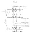
- FIG. 6 is a circuit schematic that illustrates sense amplifier circuits coupled to data cells and current reference cells according to some embodiments of the invention.
- FIG. 7 is a simplified equivalent circuit that represents sense amplifier circuits coupled to reference cells/data cells using access transistors according to some embodiments of the invention.
- FIG. 8 is an equivalent circuit showing a “crosspoint” configuration where the resistive elements represent the data cells and reference cells according to some embodiments of the invention.
- FIG. 9 is a schematic representation of a sense amplifier circuit selectively coupled to reference cells in different memory blocks according to some embodiments of the invention.
- FIG. 10 is a simplified schematic illustration of sense amplifier circuits including control transistors coupled to inputs thereof according to some embodiments of the invention.
- FIG. 11 is a schematic illustration of memory blocks including data cells and reference cells according to some embodiments of the invention.
- FIG. 12 is a simplified equivalent circuit of memory blocks including data cells and reference cells shown in FIG. 11 according to some embodiments of the invention.
- FIG. 13 is a schematic illustration of a resistive random access memory device wherein the data cells and reference cells are shown in a “crosspoint” configuration according to some embodiments of the invention.
- FIG. 14 is a simplified equivalent circuit showing the sense amplifier circuits SA 0 - 15 in FIG. 13 according to some embodiments of the invention.
- FIG. 15 is a schematic illustration of memory blocks 0 - 7 and memory blocks 8 - 15 coupled to inputs of sense amplifier circuits SA 0 - 7 according to some embodiments of the invention.
- FIG. 16 is a simplified equivalent circuit of memory blocks 0 - 7 and memory blocks 8 - 15 coupled to inputs of sense amplifier circuits SA 0 - 7 shown in FIG. 16 .
- FIG. 17 is a schematic illustration of variations in the range of distribution of currents associated with logical data values stored in data cells/reference cells.
- FIG. 18 is a schematic illustration that shows a relatively narrow distribution range for currents generated by data cells storing a logical data value of one and the current generated by memory cells storing logical data values of zero can occur over a relatively wide range.
- FIG. 19 is a schematic illustration of a reference current circuit RCB′ including three reference cells RS 1 -RS 3 coupled to four sense amplifier circuits SU 1 - 4 each providing a reference current Iref′ to the reference current circuit RCB′ according to some embodiments of the invention.
- FIG. 20 is a schematic that illustrates reference cells coupled to sense amplifier circuits SU 1 -SU 4 in some embodiments according to the invention.
- embodiments according to the invention can provide for at least three ReRAM reference cells coupled in parallel with one another and configured to provide a reference current to respective ReRAM sense amplifier circuits.
- circuits according to some embodiments of the invention can provide a relatively large number of reference cells where half are programmed with a logical data value of zero and half are programmed with a logical data value of one so that the parallel combination can provide a reference current that approximates a midpoint between reference currents associated with the logical data values of zero.
- the reference current may be less subject to process variation as the greater number of reference cells may provide a more accurate representation of a true midpoint between the data values.
- reference cells in a second block of memory are used to provide a reference current to the sense amplifier used to read the data from the first block of memory.
- either of the inputs of the sense amplifier circuits can be used to provide the reference current.
- the inputs of the sense amplifier circuits may be coupled to reference block select transistors that are configured to couple together the inputs of the sense amplifier circuits that are to be provided with the reference current.
- the input of the sense amplifier circuit that is to be coupled to the other inputs can be responsive to the block of memory to which the read operation is directed. Accordingly, a read to a first block of memory can result in data being provided to a first set of inputs of the sense amplifier circuits whereas the remaining inputs of the sense amplifier circuits are coupled to reference cells in a second block of memory.
- reference cells from different blocks can be coupled together in response to a read operation to a memory block that is outside those blocks that are coupled together.
- a read to a particular block of memory can result in reference cells from blocks other than that to which the read is directed being coupled together.
- a current reference circuit can include a number of reference cells that are configured to provide respective reference currents upon activation to a sense amplifier.
- the amounts of current provided by the reference cells can have an unequally weighted distribution of resistance values.
- the number of reference cells used to store logical data values of one may be unequal to the number of reference cells used to store a data value of zero. Accordingly, the reference circuit may be configured to compensate for a particular distribution of values provided by data cells that may be caused by particular process parameters.
- the current reference circuit may be configured so that all the reference cells store equal data values to provide substantially equal reference currents to the sense amplifier circuits coupled thereto.
- FIG. 6 is a circuit schematic that illustrates sense amplifier circuits coupled to data cells and current reference cells according to some embodiments of the invention.
- a memory block MCB includes a plurality of data cells MC that are configured to store data for subsequent retrieval during read operations performed thereto.
- the data stored in the data cells MC can be accessed through biasing of wordlines MWL 1 -M and bitlines MBL 1 -N which are coupled to the data cells MC.
- the data cells MC are configured to store logical data values based on resistive properties, such as those provided in magnetic random access memories, phase changeable random access memories, etc. Accordingly, logical data values, such as one and zero, can be stored in the data cells MC as different resistances so that upon a read operation the logical data values can be determined based on the current which flows to/from the data cells MC when the proper biasing is applied to the wordlines and bitlines coupled thereto.
- the data cells may actually represent multi-bit storage cells.
- a multi-bit arrangement at least two bits of data are stored per memory cell.
- the status of information stored in each memory cell maybe “00”, “01”, “10” or “11”.
- each memory cell may be programmed to have a threshold voltage determined as one of four different values. Accordingly, such a multi-bit memory device can store two bits in the same area as a one-bit memory device while using the number of memory cells corresponding to half the number of memory cells required in the one-bit memory device for that amount of information.
- the chip size is correspondingly reduced for storage of a given amount of information, as compared to the one-bit memory device.
- the capacity of the multi-bit memory device increases correspondingly as compared to that of the one-bit memory device.
- Multi-bit storage cells are described further in, for example, U.S. Pat. No. 6,118,696, entitled Multi-bit memory cell array of a non-volatile semiconductor memory device and method for driving the same, the entirety of which is incorporate herein by reference.
- sense amplifier circuits SU 1 -N include two inputs where one of the inputs is coupled to a respective bitline from the data cells MC in the memory block MCB.
- sense amplifier circuit SU 1 includes a first input IA 1 that is coupled to the bitline MLB 1 , which is also coupled to the first column of data cells MC in the memory block MCB.
- an input of the sense amplifier circuit SU 2 referred to as IA 2
- IA 2 is coupled to the bitline MLB 2 in the second column of data cells MC in the memory block MCB.
- a second input to each of the sense amplifier circuits SU 1 -n is coupled to a node ND. Any number of sense amplifier circuits SU can be used where each of the sense amplifier circuits is coupled to a respective bitline used to access a column in the memory block MCB.
- a reference current circuit RCB is configured to include at least three reference memory cells RC 1 -RCn coupled in parallel with one another to the node ND where each of the reference cells RC 1 -n is coupled to a reference wordline RWL. Furthermore, each of the reference cells RC 1 -n is coupled to a respective reference bitline RBL 1 -n which can be used (in combination with the reference wordline RWL) to activate the reference cells RC 1 -n in the current circuit RCB.
- a row of data cells MC in the memory block MCB can be accessed by biasing the appropriate combination of wordlines MWL 1 -m and bitlines MLB 1 -n.
- the wordline MWL 1 can be activated and a bias voltage applied to each of the bitlines MBL 1 -n to access the logical data values stored in the first row of data cells MC.
- currents IM 1 -n can be provided responsive to activation of the appropriate row of data cells MC during a read operation.
- Each of the currents IM 1 -n provided in response to the read can be proportional to the resistance provided by the respective data cell MC to which the input is connected during the read operation.
- the reference current circuit RCB can be activated by biasing of the reference word line RWL and the reference bit lines RBL 1 -n to provide substantially equal reference currents Iref sourced from each of the respective inputs to the sense amplifier circuits SU 1 -n,
- the reference currents Iref are divided among the at least three reference cells coupled in parallel with one another, which are shown in FIG. 6 as reference currents IR 1 -IRn.
- each of the sense amplifier circuits SU 1 -SUn compares the voltage levels provided to the inputs of the sense amplifier SA 1 -n that are proportional to the reference current and the current IM 1 -n that is sourced by the respective sense amplifier circuit SU 1 -n.
- each input of the sense amplifiers SA 1 -SAn is coupled to respective constant current sources IS 1 and IS 2 that can be accessed through operation of a pair of control transistors TC 1 and TC 2 that operate responsive to an output of a pair of comparators CMP 1 and CMP 2 .
- the comparators CMP 1 and CMP 2 each compare the voltage developed by the respective current Iref and IM 1 -n to a bias voltage Vb to provide operation of the control transistors TC 1 and TC 2 .
- the comparators CMP 1 and CMP 2 compare the voltage at the input (either the input coupled to the reference cells or the input connected to the data cells) to the bias voltage Vb and if the input voltage is less than the bias voltage Vb, the output of the comparitor increases so that a drain current in the control transistor TC 1 or TC 2 supplied by the constant current source IS 1 or IS 2 is increased thereby raising the voltage level presented at the input. If, on the other hand, the voltage developed at the input from the data cells MC is greater than the bias voltage Vb, the output of the comparator CMP 1 or CMP 2 decreases so that the drain current of the control transistor TC 1 or TC 2 decreases to reduce the voltage present at the input of the sense amplifier circuit SU 1 -n. It will be understood that although the operation of the circuits included in the sense amplifier circuit SU 1 -SUn are described above with reference to inputs coupled to the data cells MC, the operations of the circuits coupled to the reference cells can be analogous.
- the reference cells RC 1 -RCn included in the reference current circuit RCB can be configured so that half of the reference cells RC 1 -RCn are programmed to have a logical data value of zero, whereas the remaining reference cells RC 1 -RCn (i.e., the other half) are programmed to have a logical data value of one. Accordingly, the combined reference currents Iref provided to/from the sense amplifier circuit SU 1 -n are divided among the reference cells that are coupled in parallel with one another.
- the distribution range of the current Iref can be narrower, thereby enabling an improvement in the operating margin of the sense amplifier circuits SU 1 -n, which may further allow a more accurate determination of the data that is stored in the data cells MC.
- FIG. 7 is a simplified equivalent circuit that represents sense amplifier circuits coupled to reference cells/data cells using access transistors according to some embodiments of the invention.
- the data cells and reference cells are represented by the resistive elements coupled to the wordlines and bitlines WL/BL and reference wordline WLref and respective bitlines 0 - 15 as shown in FIG. 6 .
- the wordlines both the wordlines used to activate the data cells as well as the wordline WLref used to activate the reference cells
- the circuits described herein can operate in conjunction with access transistors as shown in FIG. 7 when the appropriate biasing is applied to the wordlines and bitlines.
- FIG. 8 is an equivalent circuit showing a “crosspoint” configuration where the resistive elements represent the data cells and reference cells as shown in FIG. 6 .
- the biasing of the wordlines coupled to the data cells along with the biasing provided to the bit lines BL 0 -BL 15 can provide for access to the data stored in the data cells.
- the reference cells can be activated responsive to biasing of the reference wordline WLref along with the bitlines.
- the selected wordline WL/WLref can have a ground voltage applied thereto while a bias voltage (of about 0.4V) is applied to the un-selected wordlines WL in conjunction with the bias voltage being applied to the bitlines.
- FIG. 9 is a schematic representation of a sense amplifier circuit selectively coupled to reference cells in different memory blocks according to some embodiments of the invention.
- the sense amplifier circuit SA is coupled to data cells and reference cells in both block 0 and in block 1 .
- the sense amplifier circuit SA can be coupled to the reference cells included in block 0 responsive to a read operation directed to data cells in block 1 .
- the sense amplifier circuit can be selectively coupled to reference cells included in, block 1 responsive to a read operation directed to data cells in memory block 0 .
- FIG. 10 is a simplified schematic illustration of sense amplifier circuits including control transistors coupled to inputs thereof.
- a first input of the sense amplifier circuits SA are coupled to control transistors which operate under control of a signal indicating a read to block 1 .
- the remaining inputs of the sense amplifier circuits SA are coupled together to control transistors that operate responsive to a signal indicating a read to block 0 .
- the upper inputs of the sense amplifier circuits can be coupled together to reference cells included in block 0 .
- the lower inputs of the sense amplifier circuits are coupled together to reference cells included in block 1 . Accordingly, a read operation directed to a particular block can cause the other inputs to the sense amplifier circuit to be coupled to reference cells in a memory block other than the block to which the read is directed.
- FIG. 11 is a schematic illustration of memory blocks including data cells and reference cells according to some embodiments of the invention.
- a first half block HBK 1 and a second half block HBK 2 each include respective row and column decoders used to activate the data cells and reference cells associated therewith.
- a first row decoder 13 A and a first column decoder 11 A are used to activate data cells and reference cells included in memory blocks MBLK 1 -MBLKi included in the first half block of HBK 1 .
- a sense amplifier block SAB includes sense amplifier circuits SU 1 -n which provide input/outputs 1 -n respectively.
- the sense amplifier circuits SU 1 -n are coupled to data cells and reference cells included in the half blocks HBK 1 and HBK 2 .
- the data cells and reference cells are coupled to respective access transistors that are used to activate the data cell/reference cell associated therewith.
- the data cells included in the first row of the half block HBK 1 can be activated by the wordline ML 1 and bitlines BL 1 -n for all memory blocks MBLK 1 -MBLKi.
- the reference cells RC 1 -RCn including memory blocks MBLK 1 -MBLKi are also controlled by respective access transistors coupled thereto.
- a read operation to one of the half blocks HBK 1 /HBK 2 can result in one of the inputs to the sense amplifier circuits SU 1 -SUn being coupled to reference cells in the other half block HBK 1 /HBK 2 .
- a read to half block HBK 1 results in data cells included in MBLK 1 -MBLKi being activated by appropriate biasing of the wordlines and bitlines coupled thereto to provide inputs to the sense amplifier circuits SU 1 -SUn.
- control signal ⁇ R 1 designates a read to the first half block HBK 1 so that the remaining inputs to the sense amplifier circuits SU-SUn are coupled to reference cells in the second half block at HBK 2 .
- the reference wordline provided by the second row decoder 13 B along with the bitlines BSL 1 -n (for both MBLK 1 and MBLKi in HBK 2 ) are used to activate the reference cells included therein.
- FIG. 11 can illustrate the use of reference cells included in memory blocks other than those to which a read operation is directed while employing access transistors to the activation of data cells and reference cells as described above in reference to FIGS. 9 and 10 , and as shown in a simplified equivalent circuit of FIG. 12 .
- FIG. 13 is a schematic illustration of a resistive random access memory device wherein the data cells and reference cells are shown in a “crosspoint” configuration as described in, for example, FIG. 8 .
- data cells included in a first row of the half block HBK 1 ′ are coupled to bitlines BL 1 -n (for both MBLK 1 ′ and MBLKi′ and are coupled to a block switching transistor TB and to a row bias unit RBU 1 for providing the proper biasing thereto in response to, for example, a read operation.
- the sense amplifier circuits included in the sense amplifier block SAB can be provided with data from the data cells from one of the half blocks HBK 1 ′/HBK 2 ′ while being coupled to reference cells included in the other half block HBK 1 ′/HBK 2 ′, which is illustrated in equivalent simplified FIG. 14 showing the sense amplifier circuits SA 0 - 15 being provided with data 0 - 31 from data cells 0 - 15 in each of the memory blocks MBLK 1 ′ and MBLK 2 ′ where each of the MBLK 1 / 2 includes sixteen data cells. Accordingly, the sense amplifier circuits SA 0 -SA 15 are also coupled to reference cells 0 - 15 included in HBK 2 ′ responsive to the read to HBK 1 ′.
- FIG. 15 is a schematic illustration of memory blocks 0 - 7 and memory blocks 8 - 15 coupled to inputs of sense amplifier circuits SA 0 - 7 , wherein the sense amplifier circuits are selectively coupled to reference cells included in a plurality of memory blocks included in memory blocks other than those to which a read operation is directed. For example, in response to a read operation to data cells included in blocks 8 - 15 , one of the inputs for each of the sense amplifier circuits SA 0 - 7 is selectively coupled to reference cells included in blocks 0 - 7 whereas the remaining inputs of the sense amplifier circuits SA 0 - 7 are selectively coupled to data cells included in memory blocks 8 - 15 , which is also illustrated in a simplified equivalent circuit of FIG. 16 .
- FIG. 17 is a schematic illustration of variations in the range of distribution of currents associated with logical data values stored in data cells/reference cells.
- FIG. 17 shows that the current associated with a program resistance of a resistive memory cell having a state corresponding to a logical data one can be a resistance that varies widely compared to variation in currents generated by cells programmed with logical data zero. Accordingly, the currents generated by cells being programmed with logical data zero can provide currents in a much narrower range than currents generated by memory cells programmed to store a logical data value of one.
- FIG. 18 is a schematic illustration that shows a relatively narrow distribution range for currents generated by data cells storing a logical data value of one and the current generated by memory cells storing logical data values of zero can occur over a relatively wide range.
- FIG. 19 is a schematic illustration of a reference current circuit RCB′ including three reference cells RS 1 -RS 3 coupled to four sense amplifier circuits SU 1 - 4 each providing a reference current Iref′ to the reference current circuit RCB′.
- all of the reference cells RS 1 - 3 can be programmed to the same state.
- each of the reference cells RS 1 -RS 3 can be programmed to either a logical data value of one or a logical data value of zero.
- the current Iref′ can be equal to about 3 ⁇ 4 of the current provided to each of the reference cells RS 1 -RS 3 .
- the reference current may be provided in an amount that is according to an unequally weighted distribution of resistance values among the reference cells.
- the reference cells can be programmed to a single value as opposed to an equal number of different values (i.e., an equal number of cells programmed to logical data value zero and logical data value one).
- the reference current used by the sense amplifiers to determine between the different data values stored in the data cells can be set according to only one of the logical data values so that an unusually wide distribution range associated with one of the logical data values can be compensated for.
- a relatively wide range of distribution for logical data value one may present problems if the reference current is generated as a midpoint between the two logical data values.
- the reference current may overlap with an upper range of the distribution of logical data value one thereby possibly generating errors when reading data cells.
- the reference current may be generated to be nearer to the logical data value one having the narrower range of distribution.
- FIG. 20 is a schematic that illustrates reference cells coupled to sense amplifier circuits SU 1 -SU 4 in some embodiments according to the invention.
- the reference cells can be arranged as a parallel arrangement where each parallel leg includes at least two reference cells in serial.
- each of the serial elements in the parallel legs can be activated by a separate reference wordline RWL 1 and RWL 2 .
- the reference current provided by the sense amplifier circuits SU 1 - 4 can thereby be generated to be about twice the current provided to each of the parallel legs of the reference current circuit RCB′′ to thereby reduce the possibility of mischaracterizing data read from the data cells in situations where the distribution of the logical data value zero/one is particularly wide as shown, for example, in FIG. 18 .
- embodiments according to the invention can provide for at least three ReRAM reference cells coupled in parallel with one another and configured to provide a reference current to respective ReRAM sense amplifier circuits.
- circuits according to some embodiments of the invention can provide a relatively large number of reference cells where half are programmed with a logical data value of zero and half are programmed with a logical data value of one so that the parallel combination can provide a reference current that approximates a midpoint between reference currents associated with the logical data values of zero.
- the reference current may be less subject to process variation as the greater number of reference cells may provide a more accurate representation of a true midpoint between the data values.
- reference cells in a second block of memory are used to provide a reference current to the sense amplifier used to read the data from the first block of memory.
- either of the inputs of the sense amplifier circuits can be used to provide the reference current.
- the inputs of the sense amplifier circuits may be coupled to reference block select transistors that are configured to couple together the inputs of the sense amplifier circuits that are to be provided with the reference current.
- the input of the sense amplifier circuit that is to be coupled to the other inputs can be responsive to the block of memory to which the read operation is directed. Accordingly, a read to a first block of memory can result in data being provided to a first set of inputs of the sense amplifier circuits whereas the remaining inputs of the sense amplifier circuits are coupled to reference cells in a second block of memory.
- reference cells from different blocks can be coupled together in response to a read operation to a memory block that is outside those blocks that are coupled together.
- a read to a particular block of memory can result in reference cells from blocks other than that to which the read is directed being coupled together.
- a current reference circuit can include a number of reference cells that are configured to provide respective reference currents upon activation to a sense amplifier.
- the amounts of current provided by the reference cells can have an unequally weighted distribution of resistance values.
- the number of reference cells used to store logical data values of one may be unequal to the number of reference cells used to store a data value of zero. Accordingly, the reference circuit may be configured to compensate for a particular distribution of values provided by data cells that may be caused by particular process parameters.
- the current reference circuit may be configured so that all the reference cells store equal data values to provide substantially equal reference currents to the sense amplifier circuits coupled thereto.
Abstract
A Resistance based Random Access Memory (ReRAM) can include a sense amplifier circuit that includes a first input coupled to a bit line of a reference cell in a first block of the ReRAM responsive to a read operation to a second block.
Description
The present application is a Divisional Application of U.S. patent application Ser. No. 12/358,936, filed in the United States Patent Office on Jan. 23, 2009, now U.S. Pat. No. 8,023,311 which is a Divisional Application of U.S. patent application Ser. No. 11/527,271, filed in the United States Patent Office on Sep. 26, 2006, now U.S. Pat. No. 7,495,984 and claims priority to Korean Patent Application No. 2005-0124033, filed in the Korean Intellectual Property Office on Dec. 15, 2005, the disclosures of which are incorporated herein by reference.
The present invention relates generally to integrated circuits and, more particularly, to resistive memory devices.
Resistive based memory devices (ReRAMs), such as magnetic random access memory (MRAM), phase changeable random access memory (PRAM), resistance random access memory (RRAM), etc. can store data by programming the resistance of cells included therein. For example, an MRAM can store a logical data value of “zero” by programming a data cell to have a relatively low resistance or can store a logical data value of “one” by programming the data cell to have a relatively high resistance as shown in FIG. 1 .
As further shown in FIG. 1 , the resistance values provided by the different values stored therein can be distributed over a range so that different memory cells exhibit different levels of resistance even though those different memory cells are programmed with the same logical data values.
When the data is read from the data cell, the programmed value can be determined by essentially comparing the programmed resistance to a reference resistance. The programmed resistance and reference resistance can actually be provided by respective currents (i.e., currents that correspond to the logical data value stored in the cell as well as the reference). Accordingly, when the data cell is read, circuitry in the MRAM can determine the level of resistance provided by the data cell being read, based on the current, to output the logical data value stored therein. MRAMs are further discussed in, for example, Durlam et al. “A low power 1 Mbit MRAM based on 1T1MTJ bit cell integrated with Copper Interconnects” 2002 Symposium on VLSI Circuits Digest of Technical Papers 158-161 (2002).
MRAMs are also discussed in, for example, Debrosse et al. “A High-Speed 128-kb MRAM Core for Future Universal Memory Applications” IEEE Journal of Solid-State Circuits 39(4):678-683 (2004).
One conventional way of determining the logical data values stored in an MRAM is discussed, for example, in U.S. Pat. No. 6,982,908 to Cho. The approach discussed in Cho uses reference cells that are programmed to store both a logical data value of zero and a logical data value of one. These reference cells are placed in parallel with one another so that a current provided by the combination (i.e., the reference current) should ideally have a value that is the midpoint between a current corresponding to a logical data value of one and a current corresponding to a logical data value of zero, as shown, for example, in FIG. 2 . For example, as shown in FIG. 2 of Cho, each of the wordlines includes a pair of reference cells where one of the pair is programmed with a logical data value of one, whereas the other reference cell in the pair is programmed with a logical data value of zero so that the combination of the two can provide a midpoint therebetween as a reference.
One of the drawbacks associated with this type of approach is that the actual current generated by reading the data cell (and the reference cell) can vary based on a bias voltage provided thereto, as shown in FIG. 3 . The Cho patent cited above also discussed an approach to reduce the effects of biasing by including two reference cells for each wordline activated for read operations, as shown, for example, in FIG. 3 of Cho.
According to FIGS. 4 and 5 , when a data cell is accessed, a current Icell is provided to a first input of the sense amplifier, whereas the reference current Iref is provided to the second input of the sense amplifier. The sense amplifier compares the voltages developed in response to the respective currents and produces a difference at the output thereof based essentially on the comparison between the reference current and the current actually provided by accessing the particular memory cell. As shown in FIG. 5 , the currents provided by the data cells (and the currents provided by the reference cells) can be spread over respective ranges.
Embodiments according to the invention can provide resistive memory devices including selected reference memory cells. Pursuant to these embodiments, a Resistance based Random Access Memory (ReRAM) can include a sense amplifier circuit that includes a first input coupled to a bit line of a reference cell in a first block of the ReRAM responsive to a read operation to a second block.
The present invention now will be described more fully hereinafter with reference to the accompanying drawings, in which embodiments of the invention are shown. However, this invention should not be construed as limited to the embodiments set forth herein. Rather, these embodiments are provided so that this disclosure will be thorough and complete, and will fully convey the scope of the invention to those skilled in the art. Like numbers refer to like elements throughout. As used herein the term “and/or” includes any and all combinations of one or more of the associated listed items.
The terminology used herein is for the purpose of describing particular embodiments only and is not intended to be limiting of the invention. As used herein, the singular forms “a”, “an” and “the” are intended to include the plural forms as well, unless the context clearly indicates otherwise. It will be further understood that the terms “comprises” and/or “comprising,” when used in this specification, specify the presence of stated features, integers, steps, operations, elements, and/or components, but do not preclude the presence or addition of one or more other features, integers, steps, operations, elements, components, and/or groups thereof.
It will be understood that when an element is referred to as being “connected” or “coupled” to another element, it can be directly connected or coupled to the other element or intervening elements may be present. In contrast, when an element is referred to as being “directly connected” or “directly coupled” to another element, there are no intervening elements present.
It will be understood that, although the terms first, second, etc. may be used herein to describe various elements, these elements should not be limited by these terms. These terms are only used to distinguish one element from another. Thus, a first element could be termed a second element without departing from the teachings of the present invention.
Unless otherwise defined, all terms (including technical and scientific terms) used herein have the same meaning as commonly understood by one of ordinary skill in the art to which this invention belongs. It will be further understood that terms, such as those defined in commonly used dictionaries, should be interpreted as having a meaning that is consistent with their meaning in the context of the relevant art and will not be interpreted in an idealized or overly formal sense unless expressly so defined herein.
As described hereinbelow in greater detail, embodiments according to the invention can provide for at least three ReRAM reference cells coupled in parallel with one another and configured to provide a reference current to respective ReRAM sense amplifier circuits. For example, circuits according to some embodiments of the invention can provide a relatively large number of reference cells where half are programmed with a logical data value of zero and half are programmed with a logical data value of one so that the parallel combination can provide a reference current that approximates a midpoint between reference currents associated with the logical data values of zero. Furthermore, the reference current may be less subject to process variation as the greater number of reference cells may provide a more accurate representation of a true midpoint between the data values.
In some embodiments according to the invention, when a read operation is performed to a first block of memory, reference cells in a second block of memory are used to provide a reference current to the sense amplifier used to read the data from the first block of memory. In still other embodiments according to the invention, either of the inputs of the sense amplifier circuits can be used to provide the reference current. In particular, the inputs of the sense amplifier circuits may be coupled to reference block select transistors that are configured to couple together the inputs of the sense amplifier circuits that are to be provided with the reference current.
Furthermore, the input of the sense amplifier circuit that is to be coupled to the other inputs can be responsive to the block of memory to which the read operation is directed. Accordingly, a read to a first block of memory can result in data being provided to a first set of inputs of the sense amplifier circuits whereas the remaining inputs of the sense amplifier circuits are coupled to reference cells in a second block of memory.
In still other embodiments according to the invention, reference cells from different blocks can be coupled together in response to a read operation to a memory block that is outside those blocks that are coupled together. In other words, a read to a particular block of memory can result in reference cells from blocks other than that to which the read is directed being coupled together.
In still further embodiments according to the invention, a current reference circuit can include a number of reference cells that are configured to provide respective reference currents upon activation to a sense amplifier. The amounts of current provided by the reference cells can have an unequally weighted distribution of resistance values. In other words, in some embodiments according to the invention, the number of reference cells used to store logical data values of one may be unequal to the number of reference cells used to store a data value of zero. Accordingly, the reference circuit may be configured to compensate for a particular distribution of values provided by data cells that may be caused by particular process parameters.
In still other embodiments according to the invention, the current reference circuit may be configured so that all the reference cells store equal data values to provide substantially equal reference currents to the sense amplifier circuits coupled thereto.
It will be understood that the data cells MC are configured to store logical data values based on resistive properties, such as those provided in magnetic random access memories, phase changeable random access memories, etc. Accordingly, logical data values, such as one and zero, can be stored in the data cells MC as different resistances so that upon a read operation the logical data values can be determined based on the current which flows to/from the data cells MC when the proper biasing is applied to the wordlines and bitlines coupled thereto.
It will be further understood that although the discussion herein discusses the storage and retrieval of single bit data in/from the data cells MC, the data cells may actually represent multi-bit storage cells. In a multi-bit arrangement, at least two bits of data are stored per memory cell. For example, in a 2-bit memory cell configuration, the status of information stored in each memory cell maybe “00”, “01”, “10” or “11”. Furthermore, each memory cell may be programmed to have a threshold voltage determined as one of four different values. Accordingly, such a multi-bit memory device can store two bits in the same area as a one-bit memory device while using the number of memory cells corresponding to half the number of memory cells required in the one-bit memory device for that amount of information. Therefore, the chip size is correspondingly reduced for storage of a given amount of information, as compared to the one-bit memory device. As the number of bits stored per memory cell increases, the capacity of the multi-bit memory device increases correspondingly as compared to that of the one-bit memory device. Multi-bit storage cells are described further in, for example, U.S. Pat. No. 6,118,696, entitled Multi-bit memory cell array of a non-volatile semiconductor memory device and method for driving the same, the entirety of which is incorporate herein by reference.
As further shown in FIG. 6 , sense amplifier circuits SU1-N include two inputs where one of the inputs is coupled to a respective bitline from the data cells MC in the memory block MCB. For example, sense amplifier circuit SU1 includes a first input IA1 that is coupled to the bitline MLB1, which is also coupled to the first column of data cells MC in the memory block MCB. Furthermore, an input of the sense amplifier circuit SU2, referred to as IA2, is coupled to the bitline MLB2 in the second column of data cells MC in the memory block MCB. As further shown in FIG. 6 , a second input to each of the sense amplifier circuits SU1-n is coupled to a node ND. Any number of sense amplifier circuits SU can be used where each of the sense amplifier circuits is coupled to a respective bitline used to access a column in the memory block MCB.
As further shown in FIG. 6 , a reference current circuit RCB is configured to include at least three reference memory cells RC1-RCn coupled in parallel with one another to the node ND where each of the reference cells RC1-n is coupled to a reference wordline RWL. Furthermore, each of the reference cells RC1-n is coupled to a respective reference bitline RBL1-n which can be used (in combination with the reference wordline RWL) to activate the reference cells RC1-n in the current circuit RCB.
In operation, a row of data cells MC in the memory block MCB can be accessed by biasing the appropriate combination of wordlines MWL1-m and bitlines MLB1-n. For example, to access the first row of data cells MC in the memory block MCB, the wordline MWL1 can be activated and a bias voltage applied to each of the bitlines MBL1-n to access the logical data values stored in the first row of data cells MC. Accordingly, currents IM1-n can be provided responsive to activation of the appropriate row of data cells MC during a read operation. Each of the currents IM1-n provided in response to the read can be proportional to the resistance provided by the respective data cell MC to which the input is connected during the read operation.
During the read operation, the reference current circuit RCB can be activated by biasing of the reference word line RWL and the reference bit lines RBL1-n to provide substantially equal reference currents Iref sourced from each of the respective inputs to the sense amplifier circuits SU1-n, The reference currents Iref are divided among the at least three reference cells coupled in parallel with one another, which are shown in FIG. 6 as reference currents IR1-IRn.
In response, each of the sense amplifier circuits SU1-SUn compares the voltage levels provided to the inputs of the sense amplifier SA1-n that are proportional to the reference current and the current IM1-n that is sourced by the respective sense amplifier circuit SU1-n. In particular, each input of the sense amplifiers SA1-SAn is coupled to respective constant current sources IS1 and IS2 that can be accessed through operation of a pair of control transistors TC1 and TC2 that operate responsive to an output of a pair of comparators CMP1 and CMP2. The comparators CMP1 and CMP2 each compare the voltage developed by the respective current Iref and IM1-n to a bias voltage Vb to provide operation of the control transistors TC1 and TC2.
The comparators CMP1 and CMP2 compare the voltage at the input (either the input coupled to the reference cells or the input connected to the data cells) to the bias voltage Vb and if the input voltage is less than the bias voltage Vb, the output of the comparitor increases so that a drain current in the control transistor TC1 or TC2 supplied by the constant current source IS1 or IS2 is increased thereby raising the voltage level presented at the input. If, on the other hand, the voltage developed at the input from the data cells MC is greater than the bias voltage Vb, the output of the comparator CMP1 or CMP2 decreases so that the drain current of the control transistor TC1 or TC2 decreases to reduce the voltage present at the input of the sense amplifier circuit SU1-n. It will be understood that although the operation of the circuits included in the sense amplifier circuit SU1-SUn are described above with reference to inputs coupled to the data cells MC, the operations of the circuits coupled to the reference cells can be analogous.
According to FIG. 6 , the reference cells RC1-RCn included in the reference current circuit RCB can be configured so that half of the reference cells RC1-RCn are programmed to have a logical data value of zero, whereas the remaining reference cells RC1-RCn (i.e., the other half) are programmed to have a logical data value of one. Accordingly, the combined reference currents Iref provided to/from the sense amplifier circuit SU1-n are divided among the reference cells that are coupled in parallel with one another.
Because an increased number of reference cells RC1-n can be provided in the reference current circuit RCB, the distribution range of the current Iref can be narrower, thereby enabling an improvement in the operating margin of the sense amplifier circuits SU1-n, which may further allow a more accurate determination of the data that is stored in the data cells MC.
As further shown in FIG. 11 , a sense amplifier block SAB includes sense amplifier circuits SU1-n which provide input/outputs 1-n respectively. The sense amplifier circuits SU1-n are coupled to data cells and reference cells included in the half blocks HBK1 and HBK2.
As further shown in FIG. 11 , the data cells and reference cells are coupled to respective access transistors that are used to activate the data cell/reference cell associated therewith. For example, the data cells included in the first row of the half block HBK1 can be activated by the wordline ML1 and bitlines BL1-n for all memory blocks MBLK1-MBLKi. Furthermore, the reference cells RC1-RCn including memory blocks MBLK1-MBLKi are also controlled by respective access transistors coupled thereto.
In operation, as discussed above in reference to FIGS. 9 and 10 , a read operation to one of the half blocks HBK1/HBK2 can result in one of the inputs to the sense amplifier circuits SU1-SUn being coupled to reference cells in the other half block HBK1/HBK2. For example, a read to half block HBK1 results in data cells included in MBLK1-MBLKi being activated by appropriate biasing of the wordlines and bitlines coupled thereto to provide inputs to the sense amplifier circuits SU1-SUn.
It will be understood that the control signal ØR1 designates a read to the first half block HBK1 so that the remaining inputs to the sense amplifier circuits SU-SUn are coupled to reference cells in the second half block at HBK2. In particular, the reference wordline provided by the second row decoder 13B along with the bitlines BSL1-n (for both MBLK1 and MBLKi in HBK2) are used to activate the reference cells included therein. Accordingly, FIG. 11 can illustrate the use of reference cells included in memory blocks other than those to which a read operation is directed while employing access transistors to the activation of data cells and reference cells as described above in reference to FIGS. 9 and 10 , and as shown in a simplified equivalent circuit of FIG. 12 .
In operation, the sense amplifier circuits included in the sense amplifier block SAB can be provided with data from the data cells from one of the half blocks HBK1′/HBK2′ while being coupled to reference cells included in the other half block HBK1′/HBK2′, which is illustrated in equivalent simplified FIG. 14 showing the sense amplifier circuits SA0-15 being provided with data 0-31 from data cells 0-15 in each of the memory blocks MBLK1′ and MBLK2′ where each of the MBLK1/2 includes sixteen data cells. Accordingly, the sense amplifier circuits SA0-SA15 are also coupled to reference cells 0-15 included in HBK2′ responsive to the read to HBK1′.
Moreover, as shown above in reference to FIG. 19 , the reference current used by the sense amplifiers to determine between the different data values stored in the data cells can be set according to only one of the logical data values so that an unusually wide distribution range associated with one of the logical data values can be compensated for. For example, as shown in FIG. 17 , a relatively wide range of distribution for logical data value one may present problems if the reference current is generated as a midpoint between the two logical data values. In other words, if the reference current is generated as the midpoint between the logical data value one and logical data value zero, it is possible that the reference current may overlap with an upper range of the distribution of logical data value one thereby possibly generating errors when reading data cells. In contrast, as shown in FIG. 18 , the reference current may be generated to be nearer to the logical data value one having the narrower range of distribution.
As described herein, embodiments according to the invention can provide for at least three ReRAM reference cells coupled in parallel with one another and configured to provide a reference current to respective ReRAM sense amplifier circuits. For example, circuits according to some embodiments of the invention can provide a relatively large number of reference cells where half are programmed with a logical data value of zero and half are programmed with a logical data value of one so that the parallel combination can provide a reference current that approximates a midpoint between reference currents associated with the logical data values of zero. Furthermore, the reference current may be less subject to process variation as the greater number of reference cells may provide a more accurate representation of a true midpoint between the data values.
In some embodiments according to the invention, when a read operation is performed to a first block of memory, reference cells in a second block of memory are used to provide a reference current to the sense amplifier used to read the data from the first block of memory. In still other embodiments according to the invention, either of the inputs of the sense amplifier circuits can be used to provide the reference current. In particular, the inputs of the sense amplifier circuits may be coupled to reference block select transistors that are configured to couple together the inputs of the sense amplifier circuits that are to be provided with the reference current.
Furthermore, the input of the sense amplifier circuit that is to be coupled to the other inputs can be responsive to the block of memory to which the read operation is directed. Accordingly, a read to a first block of memory can result in data being provided to a first set of inputs of the sense amplifier circuits whereas the remaining inputs of the sense amplifier circuits are coupled to reference cells in a second block of memory.
In still other embodiments according to the invention, reference cells from different blocks can be coupled together in response to a read operation to a memory block that is outside those blocks that are coupled together. In other words, a read to a particular block of memory can result in reference cells from blocks other than that to which the read is directed being coupled together.
In still further embodiments according to the invention, a current reference circuit can include a number of reference cells that are configured to provide respective reference currents upon activation to a sense amplifier. The amounts of current provided by the reference cells can have an unequally weighted distribution of resistance values. In other words, in some embodiments according to the invention, the number of reference cells used to store logical data values of one may be unequal to the number of reference cells used to store a data value of zero. Accordingly, the reference circuit may be configured to compensate for a particular distribution of values provided by data cells that may be caused by particular process parameters.
In still other embodiments according to the invention, the current reference circuit may be configured so that all the reference cells store equal data values to provide substantially equal reference currents to the sense amplifier circuits coupled thereto.
While the present invention has been particularly shown and described with reference to exemplary embodiments thereof, it will be understood by those of ordinary skill in the art that various changes in form and details may be made therein without departing from the spirit and scope of the present invention as defined by the following claims.
Claims (7)
1. A Resistance based Random Access Memory (ReRAM) comprising: a current reference circuit including reference cells configured to provide respective reference currents upon activation to sense amplifier circuits coupled thereto in amounts provided by an unequally weighted distribution of resistance values among the reference cells.
2. A ReRAM according to claim 1 wherein the resistance values are weighted toward a resistance value having a narrower range of values among data cells in the ReRAM.
3. A ReRAM according claim 1 wherein the ReRAM comprises a PRAM or an OxRAM, or a polymer RAM.
4. A ReRAM according to claim 1 wherein the unequally weighted distribution of resistance values is based only on one of the resistance values used to store data in the ReRAM.
5. A ReRAM according to claim 4 wherein the only one of the resistance values comprises the resistance value having a narrower range of values.
6. A ReRAM according to claim 1 wherein the current reference circuit comprises: a number of first reference cells configured to store a first resistance value; and a second number of second cells configured to store a second resistance value, wherein the first and second numbers are unequal.
7. A ReRAM according to claim 6 wherein the number of first reference cells is greater than the number of second reference cells if the range of the first resistance values is narrower than the range of the second resistance values.
Priority Applications (1)
| Application Number | Priority Date | Filing Date | Title |
|---|---|---|---|
| US13/219,582 US8345467B2 (en) | 2005-12-15 | 2011-08-26 | Resistive memory devices including selected reference memory cells operating responsive to read operations |
Applications Claiming Priority (5)
| Application Number | Priority Date | Filing Date | Title |
|---|---|---|---|
| KR2005-0124033 | 2005-12-15 | ||
| KR1020050124033A KR100735750B1 (en) | 2005-12-15 | 2005-12-15 | Semiconductor devices including a reference cell block and sense amplification units for generating a plurality of uniform reference data and systems employing the same |
| US11/527,271 US7495984B2 (en) | 2005-12-15 | 2006-09-26 | Resistive memory devices including selected reference memory cells |
| US12/358,936 US8023311B2 (en) | 2005-12-15 | 2009-01-23 | Resistive memory devices including selected reference memory cells operating responsive to read operations |
| US13/219,582 US8345467B2 (en) | 2005-12-15 | 2011-08-26 | Resistive memory devices including selected reference memory cells operating responsive to read operations |
Related Parent Applications (1)
| Application Number | Title | Priority Date | Filing Date |
|---|---|---|---|
| US12/358,936 Division US8023311B2 (en) | 2005-12-15 | 2009-01-23 | Resistive memory devices including selected reference memory cells operating responsive to read operations |
Publications (2)
| Publication Number | Publication Date |
|---|---|
| US20110310657A1 US20110310657A1 (en) | 2011-12-22 |
| US8345467B2 true US8345467B2 (en) | 2013-01-01 |
Family
ID=38173261
Family Applications (3)
| Application Number | Title | Priority Date | Filing Date |
|---|---|---|---|
| US11/527,271 Active 2027-07-07 US7495984B2 (en) | 2005-12-15 | 2006-09-26 | Resistive memory devices including selected reference memory cells |
| US12/358,936 Active 2027-05-20 US8023311B2 (en) | 2005-12-15 | 2009-01-23 | Resistive memory devices including selected reference memory cells operating responsive to read operations |
| US13/219,582 Active US8345467B2 (en) | 2005-12-15 | 2011-08-26 | Resistive memory devices including selected reference memory cells operating responsive to read operations |
Family Applications Before (2)
| Application Number | Title | Priority Date | Filing Date |
|---|---|---|---|
| US11/527,271 Active 2027-07-07 US7495984B2 (en) | 2005-12-15 | 2006-09-26 | Resistive memory devices including selected reference memory cells |
| US12/358,936 Active 2027-05-20 US8023311B2 (en) | 2005-12-15 | 2009-01-23 | Resistive memory devices including selected reference memory cells operating responsive to read operations |
Country Status (3)
| Country | Link |
|---|---|
| US (3) | US7495984B2 (en) |
| KR (1) | KR100735750B1 (en) |
| TW (1) | TWI340388B (en) |
Cited By (3)
| Publication number | Priority date | Publication date | Assignee | Title |
|---|---|---|---|---|
| US20140185401A1 (en) * | 2012-12-31 | 2014-07-03 | Taiwan Semiconductor Manufacturing Company, Ltd. | Sensing circuit, memory device and data detecting method |
| US9142292B2 (en) | 2011-02-02 | 2015-09-22 | Panasonic Intellectual Property Management Co., Ltd. | Method for reading data from nonvolatile storage element, and nonvolatile storage device |
| US11127459B1 (en) | 2020-03-16 | 2021-09-21 | Globalfoundries Singapore Pte. Ltd. | Memory devices and methods of forming the same |
Families Citing this family (88)
| Publication number | Priority date | Publication date | Assignee | Title |
|---|---|---|---|---|
| US8664124B2 (en) | 2005-10-31 | 2014-03-04 | Novellus Systems, Inc. | Method for etching organic hardmasks |
| JP4987616B2 (en) * | 2006-08-31 | 2012-07-25 | 株式会社東芝 | Magnetic random access memory and resistive random access memory |
| US7701759B2 (en) | 2007-02-05 | 2010-04-20 | Macronix International Co., Ltd. | Memory cell device and programming methods |
| US7915166B1 (en) | 2007-02-22 | 2011-03-29 | Novellus Systems, Inc. | Diffusion barrier and etch stop films |
| WO2008126166A1 (en) * | 2007-03-09 | 2008-10-23 | Fujitsu Limited | Nonvolatile semiconductor storage device and reading method thereof |
| US7630262B2 (en) * | 2007-07-04 | 2009-12-08 | Hynix Semiconductor, Inc. | One-transistor type dram |
| KR100861190B1 (en) * | 2007-07-04 | 2008-09-30 | 주식회사 하이닉스반도체 | One transistor type dram |
| KR101367659B1 (en) * | 2007-07-12 | 2014-02-25 | 삼성전자주식회사 | Multi-level phase change memory device for reducing read error and read method thereof |
| US8962101B2 (en) | 2007-08-31 | 2015-02-24 | Novellus Systems, Inc. | Methods and apparatus for plasma-based deposition |
| KR100895389B1 (en) * | 2007-09-06 | 2009-04-30 | 주식회사 하이닉스반도체 | Phase change memory device |
| JP2009087494A (en) * | 2007-10-02 | 2009-04-23 | Toshiba Corp | Magnetic random access memory |
| US7778065B2 (en) * | 2008-02-29 | 2010-08-17 | International Business Machines Corporation | Method and apparatus for implementing concurrent multiple level sensing operation for resistive memory devices |
| US8077505B2 (en) | 2008-05-07 | 2011-12-13 | Macronix International Co., Ltd. | Bipolar switching of phase change device |
| US8134857B2 (en) | 2008-06-27 | 2012-03-13 | Macronix International Co., Ltd. | Methods for high speed reading operation of phase change memory and device employing same |
| US8435608B1 (en) | 2008-06-27 | 2013-05-07 | Novellus Systems, Inc. | Methods of depositing smooth and conformal ashable hard mask films |
| JP2010055719A (en) * | 2008-08-29 | 2010-03-11 | Toshiba Corp | Resistance change memory device |
| US7719913B2 (en) * | 2008-09-12 | 2010-05-18 | Macronix International Co., Ltd. | Sensing circuit for PCRAM applications |
| US8036014B2 (en) | 2008-11-06 | 2011-10-11 | Macronix International Co., Ltd. | Phase change memory program method without over-reset |
| US7869270B2 (en) * | 2008-12-29 | 2011-01-11 | Macronix International Co., Ltd. | Set algorithm for phase change memory cell |
| US8093661B2 (en) * | 2009-01-07 | 2012-01-10 | Macronix International Co., Ltd. | Integrated circuit device with single crystal silicon on silicide and manufacturing method |
| US8107283B2 (en) | 2009-01-12 | 2012-01-31 | Macronix International Co., Ltd. | Method for setting PCRAM devices |
| US8064247B2 (en) | 2009-01-14 | 2011-11-22 | Macronix International Co., Ltd. | Rewritable memory device based on segregation/re-absorption |
| US8406033B2 (en) | 2009-06-22 | 2013-03-26 | Macronix International Co., Ltd. | Memory device and method for sensing and fixing margin cells |
| KR20100137884A (en) * | 2009-06-23 | 2010-12-31 | 삼성전자주식회사 | Variable resistive memory device compensating wordline resistance |
| US8269203B2 (en) | 2009-07-02 | 2012-09-18 | Actel Corporation | Resistive RAM devices for programmable logic devices |
| US7894254B2 (en) | 2009-07-15 | 2011-02-22 | Macronix International Co., Ltd. | Refresh circuitry for phase change memory |
| US8494430B2 (en) * | 2009-09-10 | 2013-07-23 | Xerox Corporation | Apparatus and method for the registration and de-skew of substrate media |
| US8563414B1 (en) | 2010-04-23 | 2013-10-22 | Novellus Systems, Inc. | Methods for forming conductive carbon films by PECVD |
| US8634235B2 (en) | 2010-06-25 | 2014-01-21 | Macronix International Co., Ltd. | Phase change memory coding |
| US8587994B2 (en) * | 2010-09-08 | 2013-11-19 | Qualcomm Incorporated | System and method for shared sensing MRAM |
| US8605520B2 (en) * | 2010-09-22 | 2013-12-10 | Magic Technologies, Inc. | Replaceable, precise-tracking reference lines for memory products |
| US8467238B2 (en) | 2010-11-15 | 2013-06-18 | Macronix International Co., Ltd. | Dynamic pulse operation for phase change memory |
| US8559243B2 (en) * | 2010-11-22 | 2013-10-15 | Infineon Technologies Ag | Self timed current integrating scheme employing level and slope detection |
| KR20120059991A (en) | 2010-12-01 | 2012-06-11 | 삼성전자주식회사 | Memory device, test operation method thereof, and system having the same |
| JP5673935B2 (en) * | 2010-12-28 | 2015-02-18 | セイコーエプソン株式会社 | Nonvolatile storage device, electronic device |
| US8374019B2 (en) | 2011-01-05 | 2013-02-12 | Macronix International Co., Ltd. | Phase change memory with fast write characteristics |
| US8891293B2 (en) | 2011-06-23 | 2014-11-18 | Macronix International Co., Ltd. | High-endurance phase change memory devices and methods for operating the same |
| WO2013027347A1 (en) * | 2011-08-24 | 2013-02-28 | パナソニック株式会社 | Semiconductor recording device |
| KR20140047732A (en) | 2011-08-26 | 2014-04-22 | 휴렛-팩커드 디벨롭먼트 컴퍼니, 엘.피. | Circuit and method for reading a resistive switching device in an array |
| JP5877338B2 (en) | 2011-08-31 | 2016-03-08 | パナソニックIpマネジメント株式会社 | Read circuit and nonvolatile memory using the same |
| US8675390B2 (en) | 2011-10-21 | 2014-03-18 | Qualcomm Incorporated | System and method for MRAM having controlled averagable and isolatable voltage reference |
| US9343146B2 (en) | 2012-01-10 | 2016-05-17 | Micron Technology, Inc. | Apparatuses and methods for low power current mode sense amplification |
| US9001550B2 (en) | 2012-04-27 | 2015-04-07 | Macronix International Co., Ltd. | Blocking current leakage in a memory array |
| SG195494A1 (en) | 2012-05-18 | 2013-12-30 | Novellus Systems Inc | Carbon deposition-etch-ash gap fill process |
| US8644060B2 (en) * | 2012-06-07 | 2014-02-04 | Avalanche Technology, Inc. | Method of sensing data of a magnetic random access memories (MRAM) |
| JP5966150B2 (en) * | 2012-07-31 | 2016-08-10 | パナソニックIpマネジメント株式会社 | Nonvolatile memory element driving method and nonvolatile memory device |
| US20140071747A1 (en) | 2012-09-07 | 2014-03-13 | Being Advanced Memory Corporation | Processors and Systems with Multicell Multibit Phase-Change Memory |
| US9362133B2 (en) | 2012-12-14 | 2016-06-07 | Lam Research Corporation | Method for forming a mask by etching conformal film on patterned ashable hardmask |
| KR101545512B1 (en) | 2012-12-26 | 2015-08-24 | 성균관대학교산학협력단 | Semiconductor memory apparatus, verify read method and system |
| KR102060488B1 (en) | 2012-12-27 | 2019-12-30 | 삼성전자주식회사 | Non-volatile random access memory device and data read method thereof |
| US8964442B2 (en) | 2013-01-14 | 2015-02-24 | Macronix International Co., Ltd. | Integrated circuit 3D phase change memory array and manufacturing method |
| KR102079370B1 (en) | 2013-02-05 | 2020-02-20 | 삼성전자주식회사 | Nonvolatile memory device and writing method thereof |
| KR101470520B1 (en) * | 2013-02-12 | 2014-12-08 | 성균관대학교산학협력단 | Semiconductor memory apparatus, read method and system |
| US9304396B2 (en) | 2013-02-25 | 2016-04-05 | Lam Research Corporation | PECVD films for EUV lithography |
| US9099191B2 (en) * | 2013-06-04 | 2015-08-04 | Ememory Technology Inc. | Current sensing amplifier and sensing method thereof |
| US9589799B2 (en) | 2013-09-30 | 2017-03-07 | Lam Research Corporation | High selectivity and low stress carbon hardmask by pulsed low frequency RF power |
| US9320387B2 (en) | 2013-09-30 | 2016-04-26 | Lam Research Corporation | Sulfur doped carbon hard masks |
| TWI503842B (en) * | 2013-11-28 | 2015-10-11 | Winbond Electronics Corp | Resistive memory apparatus and memory cell thereof |
| CN104733611B (en) * | 2013-12-24 | 2017-09-05 | 华邦电子股份有限公司 | Resistive memory device and its memory cell |
| WO2015126518A2 (en) * | 2014-02-20 | 2015-08-27 | Rambus Inc. | High performance persistent memory |
| US9761309B2 (en) * | 2014-02-28 | 2017-09-12 | Hewlett Packard Enterprise Development Lp | Sensing circuit for resistive memory array |
| US9424914B2 (en) | 2014-03-19 | 2016-08-23 | Winbond Electronics Corp. | Resistive memory apparatus and memory cell thereof |
| GB2524534A (en) | 2014-03-26 | 2015-09-30 | Ibm | Determining a cell state of a resistive memory cell |
| US9312002B2 (en) | 2014-04-04 | 2016-04-12 | Sandisk Technologies Inc. | Methods for programming ReRAM devices |
| KR102111510B1 (en) | 2014-04-10 | 2020-05-19 | 에스케이하이닉스 주식회사 | Electronic device |
| KR102116879B1 (en) * | 2014-05-19 | 2020-06-01 | 에스케이하이닉스 주식회사 | Electronic device |
| US9064569B1 (en) | 2014-07-03 | 2015-06-23 | Sandisk Technologies Inc. | Memory controller with resistive random access memory (ReRAM) |
| KR102212750B1 (en) | 2014-07-23 | 2021-02-05 | 삼성전자주식회사 | Resistive memory device, memory system including the same and method of reading data in resistive memory device |
| US10079059B2 (en) | 2014-07-28 | 2018-09-18 | Hewlett Packard Enterprise Development Lp | Memristor cell read margin enhancement |
| US10032509B2 (en) * | 2015-03-30 | 2018-07-24 | Toshiba Memory Corporation | Semiconductor memory device including variable resistance element |
| US9666273B2 (en) | 2015-06-18 | 2017-05-30 | International Business Machines Corporation | Determining a cell state of a resistive memory cell |
| US9779810B2 (en) | 2015-09-11 | 2017-10-03 | Macronix International Co., Ltd. | Adjustable writing circuit |
| US10490270B2 (en) | 2015-10-28 | 2019-11-26 | Hewlett Packard Enterprise Development Lp | Reference column sensing for resistive memory |
| US9520189B1 (en) | 2015-10-29 | 2016-12-13 | International Business Machines Corporation | Enhanced temperature compensation for resistive memory cell circuits |
| US9659624B1 (en) * | 2016-03-15 | 2017-05-23 | Avago Technologies General Ip (Singapore) Pte. Ltd. | Method for sense reference generation for MTJ based memories |
| US10170182B2 (en) | 2016-03-16 | 2019-01-01 | Imec Vzw | Resistance change memory device configured for state evaluation based on reference cells |
| US9666259B1 (en) * | 2016-04-12 | 2017-05-30 | Qualcomm Incorporated | Dual mode sensing scheme |
| US10430534B2 (en) * | 2016-11-30 | 2019-10-01 | Numem Inc. | Resistance-based memory compiler |
| TWI645402B (en) * | 2017-01-20 | 2018-12-21 | 旺宏電子股份有限公司 | Semiconductor memory device and operation method thereof |
| DE112018004134T5 (en) * | 2017-08-11 | 2020-04-23 | Microsemi Soc Corp. | CIRCUIT LOGIC AND METHOD FOR PROGRAMMING RESISTIVE DIRECT ACCESS STORAGE DEVICES |
| KR102422252B1 (en) * | 2017-11-15 | 2022-07-19 | 에스케이하이닉스 주식회사 | Memory device |
| US10242737B1 (en) * | 2018-02-13 | 2019-03-26 | Macronix International Co., Ltd. | Device structure for neuromorphic computing system |
| TW202113121A (en) | 2019-05-29 | 2021-04-01 | 美商蘭姆研究公司 | High selectivity, low stress, and low hydrogen diamond-like carbon hardmasks by high power pulsed low frequency rf |
| US10803913B1 (en) * | 2019-06-11 | 2020-10-13 | Applied Materials, Inc. | Narrow range sense amplifier with immunity to noise and variation |
| US11289144B1 (en) | 2020-09-25 | 2022-03-29 | Nxp Usa, Inc. | Non-volatile memory with virtual ground voltage provided to unselected column lines during memory write operation |
| US11348628B2 (en) * | 2020-09-25 | 2022-05-31 | Nxp Usa, Inc. | Non-volatle memory with virtual ground voltage provided to unselected column lines during memory read operation |
| US11605418B2 (en) * | 2020-10-26 | 2023-03-14 | Micron Technology, Inc. | Memory device architecture using multiple physical cells per bit to improve read margin and to alleviate the need for managing demarcation read voltages |
| TWI816628B (en) * | 2023-02-17 | 2023-09-21 | 環宇積體電路股份有限公司 | Resistive memory and how to operate it |
Citations (45)
| Publication number | Priority date | Publication date | Assignee | Title |
|---|---|---|---|---|
| JPH02110895A (en) | 1988-10-19 | 1990-04-24 | Toshiba Corp | Semiconductor memory |
| US5432731A (en) | 1993-03-08 | 1995-07-11 | Motorola, Inc. | Ferroelectric memory cell and method of sensing and writing the polarization state thereof |
| JPH0997496A (en) | 1995-09-29 | 1997-04-08 | Nec Corp | Ferroelectric substance memory device and data reading method |
| US5753946A (en) | 1995-02-22 | 1998-05-19 | Sony Corporation | Ferroelectric memory |
| US5999439A (en) | 1995-09-11 | 1999-12-07 | Micron Technology, Inc. | Ferroelectric memory using ferroelectric reference cells |
| US6246622B1 (en) | 1999-07-30 | 2001-06-12 | Nec Corporation | Semiconductor memory device |
| US6269040B1 (en) | 2000-06-26 | 2001-07-31 | International Business Machines Corporation | Interconnection network for connecting memory cells to sense amplifiers |
| US6317376B1 (en) | 2000-06-20 | 2001-11-13 | Hewlett-Packard Company | Reference signal generation for magnetic random access memory devices |
| US6317375B1 (en) | 2000-08-31 | 2001-11-13 | Hewlett-Packard Company | Method and apparatus for reading memory cells of a resistive cross point array |
| KR20020003296A (en) | 2000-07-03 | 2002-01-12 | 추후제출 | Integrated memory with memory cells with magnetoresistive effect and method for operating the memory |
| US6426907B1 (en) | 2001-01-24 | 2002-07-30 | Infineon Technologies North America Corp. | Reference for MRAM cell |
| JP2002343077A (en) | 2001-05-16 | 2002-11-29 | Mitsubishi Electric Corp | Thin film magnetic storage device |
| US6490217B1 (en) | 2001-05-23 | 2002-12-03 | International Business Machines Corporation | Select line architecture for magnetic random access memories |
| JP2003196973A (en) | 2001-12-21 | 2003-07-11 | Mitsubishi Electric Corp | Thin film magnetic material storage device |
| DE10304453A1 (en) | 2002-02-04 | 2003-08-21 | Mitsubishi Electric Corp | Magnetic thin film storage device |
| JP2003257175A (en) | 2001-12-28 | 2003-09-12 | Nec Corp | Semiconductor memory device using tunnel magnetoresistive elements |
| JP2003257177A (en) | 2001-12-28 | 2003-09-12 | Toshiba Corp | Magnetic random access memory |
| JP2003288779A (en) | 2002-02-25 | 2003-10-10 | Hewlett Packard Co <Hp> | Method and system for removing leakage current by carrying out sensing equipotential sensing across memory array |
| JP2003297072A (en) | 2002-04-03 | 2003-10-17 | Mitsubishi Electric Corp | Thin film magnetic storage device |
| US20030235071A1 (en) | 2002-06-20 | 2003-12-25 | Takeshi Okazawa | Magnetic memory device having XP cell and STr cell in one chip |
| JP2004005797A (en) | 2002-05-30 | 2004-01-08 | Mitsubishi Electric Corp | Thin film magnetic substance memory device |
| US6738285B2 (en) | 2002-01-30 | 2004-05-18 | Renesas Technology Corp. | Thin film magnetic memory device with high-accuracy data read structure having a reduced number of circuit elements |
| US6757191B2 (en) | 2001-09-21 | 2004-06-29 | Renesas Technology Corp. | Thin film magnetic memory device sharing an access element by a plurality of memory cells |
| US6778426B2 (en) | 2001-08-08 | 2004-08-17 | Kabushiki Kaisha Toshiba | Magnetic random access memory including memory cell unit and reference cell unit |
| US6795340B2 (en) | 2002-01-10 | 2004-09-21 | Nec Corporation | Non-volatile magnetic memory |
| US20040233709A1 (en) | 2003-05-22 | 2004-11-25 | Kenji Tsuchida | MRAM having memory cell array in which cross-point memory cells are arranged by hierarchical bit line scheme and data read method thereof |
| US6839269B2 (en) | 2001-12-28 | 2005-01-04 | Kabushiki Kaisha Toshiba | Magnetic random access memory |
| KR20050004160A (en) | 2002-05-22 | 2005-01-12 | 코닌클리즈케 필립스 일렉트로닉스 엔.브이. | Magnetoresistive memory cell array and mram memory comprising such array |
| JP2005018916A (en) | 2003-06-26 | 2005-01-20 | Toshiba Corp | Magnetic random access memory |
| US6870759B2 (en) | 2002-12-09 | 2005-03-22 | Applied Spintronics Technology, Inc. | MRAM array with segmented magnetic write lines |
| US20050105329A1 (en) | 2003-11-04 | 2005-05-19 | Nazarian Hagop A. | Serial transistor-cell array architecture |
| US20050128793A1 (en) | 2003-12-12 | 2005-06-16 | Ho Chiahua | Method and apparatus for a low write current MRAM having a write magnet |
| US6982908B2 (en) | 2002-08-02 | 2006-01-03 | Samsung Electronics Co., Ltd. | Magnetic random access memory device capable of providing a constant current to a reference cell |
| US20060062066A1 (en) | 2004-09-17 | 2006-03-23 | Garni Bradley J | Mram sense amplifier having a precharge circuit and method for sensing |
| US7027342B2 (en) | 2004-06-15 | 2006-04-11 | Sharp Kabushiki Kaisha | Semiconductor memory device |
| US7116598B2 (en) | 2004-09-28 | 2006-10-03 | Kabushiki Kaisha Toshiba | Semiconductor memory |
| US7313043B2 (en) | 2005-11-29 | 2007-12-25 | Altis Semiconductor Snc | Magnetic Memory Array |
| US20090323405A1 (en) * | 2008-06-30 | 2009-12-31 | Qualcomm Incorporated | Controlled Value Reference Signal of Resistance Based Memory Circuit |
| US20100046274A1 (en) * | 2008-08-20 | 2010-02-25 | Kabushiki Kaisha Toshiba | Resistance change memory |
| US20100054020A1 (en) | 2008-09-04 | 2010-03-04 | Kabushiki Kaisha Toshiba | Semiconductor memory device |
| US20100195415A1 (en) | 2009-02-04 | 2010-08-05 | Elpida Memory, Inc. | Semiconductor memory device and reading method therefor |
| US20100271861A1 (en) | 2009-04-22 | 2010-10-28 | Sony Corporation | Variable-resistance memory device and its operation method |
| US20110080775A1 (en) * | 2006-09-05 | 2011-04-07 | Jun-Soo Bae | Nonvolatile memory device, storage system having the same, and method of driving the nonvolatile memory device |
| US20110310661A1 (en) * | 2008-09-12 | 2011-12-22 | Micron Technology, Inc. | Memory sensing devices, methods, and systems |
| US20120087183A1 (en) * | 2010-10-12 | 2012-04-12 | Samsung Electronics Co., Ltd. | Methods of operating prams using initial programmed resistances and prams using the same |
-
2005
- 2005-12-15 KR KR1020050124033A patent/KR100735750B1/en active IP Right Grant
-
2006
- 2006-09-26 US US11/527,271 patent/US7495984B2/en active Active
- 2006-12-14 TW TW095146843A patent/TWI340388B/en active
-
2009
- 2009-01-23 US US12/358,936 patent/US8023311B2/en active Active
-
2011
- 2011-08-26 US US13/219,582 patent/US8345467B2/en active Active
Patent Citations (63)
| Publication number | Priority date | Publication date | Assignee | Title |
|---|---|---|---|---|
| JPH02110895A (en) | 1988-10-19 | 1990-04-24 | Toshiba Corp | Semiconductor memory |
| US5432731A (en) | 1993-03-08 | 1995-07-11 | Motorola, Inc. | Ferroelectric memory cell and method of sensing and writing the polarization state thereof |
| US5753946A (en) | 1995-02-22 | 1998-05-19 | Sony Corporation | Ferroelectric memory |
| US5999439A (en) | 1995-09-11 | 1999-12-07 | Micron Technology, Inc. | Ferroelectric memory using ferroelectric reference cells |
| JPH0997496A (en) | 1995-09-29 | 1997-04-08 | Nec Corp | Ferroelectric substance memory device and data reading method |
| US6246622B1 (en) | 1999-07-30 | 2001-06-12 | Nec Corporation | Semiconductor memory device |
| US6317376B1 (en) | 2000-06-20 | 2001-11-13 | Hewlett-Packard Company | Reference signal generation for magnetic random access memory devices |
| US6269040B1 (en) | 2000-06-26 | 2001-07-31 | International Business Machines Corporation | Interconnection network for connecting memory cells to sense amplifiers |
| US6504751B2 (en) | 2000-07-03 | 2003-01-07 | Infineon Technologies Ag | Integrated memory having memory cells with a magnetoresistive storage property and method of operating such a memory |
| KR20020003296A (en) | 2000-07-03 | 2002-01-12 | 추후제출 | Integrated memory with memory cells with magnetoresistive effect and method for operating the memory |
| KR100449067B1 (en) | 2000-07-03 | 2004-09-16 | 인피니언 테크놀로지스 아게 | Integrated memory with memory cells with magnetoresistive effect and method for operating the memory |
| US6317375B1 (en) | 2000-08-31 | 2001-11-13 | Hewlett-Packard Company | Method and apparatus for reading memory cells of a resistive cross point array |
| JP2002140888A (en) | 2000-08-31 | 2002-05-17 | Hewlett Packard Co <Hp> | Information storing device |
| US6426907B1 (en) | 2001-01-24 | 2002-07-30 | Infineon Technologies North America Corp. | Reference for MRAM cell |
| JP2002343077A (en) | 2001-05-16 | 2002-11-29 | Mitsubishi Electric Corp | Thin film magnetic storage device |
| US7116595B2 (en) | 2001-05-16 | 2006-10-03 | Renesas Technology Corp. | Thin film magnetic memory device having a magnetic tunnel junction |
| US6876575B2 (en) | 2001-05-16 | 2005-04-05 | Renesas Technology Corp. | Thin film magnetic memory device having a magnetic tunnel junction |
| US6490217B1 (en) | 2001-05-23 | 2002-12-03 | International Business Machines Corporation | Select line architecture for magnetic random access memories |
| US6778426B2 (en) | 2001-08-08 | 2004-08-17 | Kabushiki Kaisha Toshiba | Magnetic random access memory including memory cell unit and reference cell unit |
| US6757191B2 (en) | 2001-09-21 | 2004-06-29 | Renesas Technology Corp. | Thin film magnetic memory device sharing an access element by a plurality of memory cells |
| JP2003196973A (en) | 2001-12-21 | 2003-07-11 | Mitsubishi Electric Corp | Thin film magnetic material storage device |
| US7272064B2 (en) | 2001-12-21 | 2007-09-18 | Renesas Technology Corp. | Thin film magnetic memory device for writing data of a plurality of bits in parallel |
| US7072207B2 (en) | 2001-12-21 | 2006-07-04 | Renesas Technology Corp. | Thin film magnetic memory device for writing data of a plurality of bits in parallel |
| US6714443B2 (en) | 2001-12-21 | 2004-03-30 | Renesas Technology Corp. | Thin film magnetic memory device for writing data of a plurality of bits in parallel |
| JP2003257177A (en) | 2001-12-28 | 2003-09-12 | Toshiba Corp | Magnetic random access memory |
| US6990015B2 (en) | 2001-12-28 | 2006-01-24 | Nec Corporation | Semiconductor memory device using tunneling magnetoresistive elements |
| JP2003257175A (en) | 2001-12-28 | 2003-09-12 | Nec Corp | Semiconductor memory device using tunnel magnetoresistive elements |
| US20050036376A1 (en) | 2001-12-28 | 2005-02-17 | Yoshihisa Iwata | Magnetic random access memory |
| US6839269B2 (en) | 2001-12-28 | 2005-01-04 | Kabushiki Kaisha Toshiba | Magnetic random access memory |
| US6795340B2 (en) | 2002-01-10 | 2004-09-21 | Nec Corporation | Non-volatile magnetic memory |
| US6738285B2 (en) | 2002-01-30 | 2004-05-18 | Renesas Technology Corp. | Thin film magnetic memory device with high-accuracy data read structure having a reduced number of circuit elements |
| DE10304453A1 (en) | 2002-02-04 | 2003-08-21 | Mitsubishi Electric Corp | Magnetic thin film storage device |
| US6826079B2 (en) | 2002-02-25 | 2004-11-30 | Hewlett-Packard Development Company, L.P. | Method and system for performing equipotential sensing across a memory array to eliminate leakage currents |
| JP2003288779A (en) | 2002-02-25 | 2003-10-10 | Hewlett Packard Co <Hp> | Method and system for removing leakage current by carrying out sensing equipotential sensing across memory array |
| US6678189B2 (en) | 2002-02-25 | 2004-01-13 | Hewlett-Packard Development Company, L.P. | Method and system for performing equipotential sensing across a memory array to eliminate leakage currents |
| US7233537B2 (en) | 2002-04-03 | 2007-06-19 | Renesas Technology Corp. | Thin film magnetic memory device provided with a dummy cell for data read reference |
| JP2003297072A (en) | 2002-04-03 | 2003-10-17 | Mitsubishi Electric Corp | Thin film magnetic storage device |
| KR20050004160A (en) | 2002-05-22 | 2005-01-12 | 코닌클리즈케 필립스 일렉트로닉스 엔.브이. | Magnetoresistive memory cell array and mram memory comprising such array |
| JP2004005797A (en) | 2002-05-30 | 2004-01-08 | Mitsubishi Electric Corp | Thin film magnetic substance memory device |
| US6856537B2 (en) | 2002-05-30 | 2005-02-15 | Renesas Technology Corp. | Thin film magnetic memory device having dummy cell |
| JP2004023062A (en) | 2002-06-20 | 2004-01-22 | Nec Electronics Corp | Semiconductor device and method for manufacturing the same |
| US20030235071A1 (en) | 2002-06-20 | 2003-12-25 | Takeshi Okazawa | Magnetic memory device having XP cell and STr cell in one chip |
| KR20030097697A (en) | 2002-06-20 | 2003-12-31 | 엔이씨 일렉트로닉스 코포레이션 | Magnetic memory device having xp cell and str cell in one chip |
| US6982908B2 (en) | 2002-08-02 | 2006-01-03 | Samsung Electronics Co., Ltd. | Magnetic random access memory device capable of providing a constant current to a reference cell |
| US6870759B2 (en) | 2002-12-09 | 2005-03-22 | Applied Spintronics Technology, Inc. | MRAM array with segmented magnetic write lines |
| US20040233709A1 (en) | 2003-05-22 | 2004-11-25 | Kenji Tsuchida | MRAM having memory cell array in which cross-point memory cells are arranged by hierarchical bit line scheme and data read method thereof |
| JP2005018916A (en) | 2003-06-26 | 2005-01-20 | Toshiba Corp | Magnetic random access memory |
| US20050105329A1 (en) | 2003-11-04 | 2005-05-19 | Nazarian Hagop A. | Serial transistor-cell array architecture |
| US7286378B2 (en) | 2003-11-04 | 2007-10-23 | Micron Technology, Inc. | Serial transistor-cell array architecture |
| US20050128793A1 (en) | 2003-12-12 | 2005-06-16 | Ho Chiahua | Method and apparatus for a low write current MRAM having a write magnet |
| US7027342B2 (en) | 2004-06-15 | 2006-04-11 | Sharp Kabushiki Kaisha | Semiconductor memory device |
| US20060062066A1 (en) | 2004-09-17 | 2006-03-23 | Garni Bradley J | Mram sense amplifier having a precharge circuit and method for sensing |
| US7116598B2 (en) | 2004-09-28 | 2006-10-03 | Kabushiki Kaisha Toshiba | Semiconductor memory |
| US7313043B2 (en) | 2005-11-29 | 2007-12-25 | Altis Semiconductor Snc | Magnetic Memory Array |
| US20110080775A1 (en) * | 2006-09-05 | 2011-04-07 | Jun-Soo Bae | Nonvolatile memory device, storage system having the same, and method of driving the nonvolatile memory device |
| US20090323405A1 (en) * | 2008-06-30 | 2009-12-31 | Qualcomm Incorporated | Controlled Value Reference Signal of Resistance Based Memory Circuit |
| US20100046274A1 (en) * | 2008-08-20 | 2010-02-25 | Kabushiki Kaisha Toshiba | Resistance change memory |
| US8189363B2 (en) * | 2008-08-20 | 2012-05-29 | Kabushiki Kaisha Toshiba | Resistance change memory |
| US20100054020A1 (en) | 2008-09-04 | 2010-03-04 | Kabushiki Kaisha Toshiba | Semiconductor memory device |
| US20110310661A1 (en) * | 2008-09-12 | 2011-12-22 | Micron Technology, Inc. | Memory sensing devices, methods, and systems |
| US20100195415A1 (en) | 2009-02-04 | 2010-08-05 | Elpida Memory, Inc. | Semiconductor memory device and reading method therefor |
| US20100271861A1 (en) | 2009-04-22 | 2010-10-28 | Sony Corporation | Variable-resistance memory device and its operation method |
| US20120087183A1 (en) * | 2010-10-12 | 2012-04-12 | Samsung Electronics Co., Ltd. | Methods of operating prams using initial programmed resistances and prams using the same |
Non-Patent Citations (10)
| Title |
|---|
| German Office Action corresponding to German Patent Application No. 10 2006 053 744.0 dated Oct. 12, 2010; 7 pages. |
| John DeBrosse et al.; A High-Speed 128-kb MRAM Core for Future Universal Memory Applications; IEEE Journal of Solid-State Circuits, vol. 39. No. 4; Apr. 2004, pp. 678-683. |
| Korean Office Action for corresponding Korean Patent Application No. 10-2005-0124033, 2 pages, (Nov. 20, 2006). |
| M. Durlam et al; IEEE 2002 Symposium on VLSI Circuits Digest of Technical Papers; pp. 158-161. |
| Notice of Allowability for Korean Patent Application No. 10-2005-0107178; May 31, 2007. |
| Notice of Allowability for Korean Patent Application No. 10-2005-0124033; May 28, 2007. |
| Taiwanese First Office Action and English translation (12 pages) corresponding to Taiwanese Patent Application No. 095141271; Issue Date: Jun. 12, 2009. |
| Taiwanese First Office Action and English translation (18 pages) corresponding to Taiwanese Patent Application No. 095141271; Dated: Dec. 17, 2008. |
| Taiwanese Office Action corresponding to Taiwan Patent Application No. 095146843 dated Dec. 3, 2009; 13 pages. |
| Taiwanese Preliminary Notice of First Office Action and English translation (5 pages) corresponding to Taiwanese Patent Application No. 095146843; Issue Date: Jul. 13, 2009. |
Cited By (4)
| Publication number | Priority date | Publication date | Assignee | Title |
|---|---|---|---|---|
| US9142292B2 (en) | 2011-02-02 | 2015-09-22 | Panasonic Intellectual Property Management Co., Ltd. | Method for reading data from nonvolatile storage element, and nonvolatile storage device |
| US20140185401A1 (en) * | 2012-12-31 | 2014-07-03 | Taiwan Semiconductor Manufacturing Company, Ltd. | Sensing circuit, memory device and data detecting method |
| US9437257B2 (en) * | 2012-12-31 | 2016-09-06 | Taiwan Semiconductor Manufacturing Company, Ltd. | Sensing circuit, memory device and data detecting method |
| US11127459B1 (en) | 2020-03-16 | 2021-09-21 | Globalfoundries Singapore Pte. Ltd. | Memory devices and methods of forming the same |
Also Published As
| Publication number | Publication date |
|---|---|
| KR20070063801A (en) | 2007-06-20 |
| KR100735750B1 (en) | 2007-07-06 |
| US20090135642A1 (en) | 2009-05-28 |
| US7495984B2 (en) | 2009-02-24 |
| US20110310657A1 (en) | 2011-12-22 |
| US8023311B2 (en) | 2011-09-20 |
| TW200729216A (en) | 2007-08-01 |
| US20070140029A1 (en) | 2007-06-21 |
| TWI340388B (en) | 2011-04-11 |
Similar Documents
| Publication | Publication Date | Title |
|---|---|---|
| US8345467B2 (en) | Resistive memory devices including selected reference memory cells operating responsive to read operations | |
| JP4153901B2 (en) | Semiconductor memory device | |
| US10269404B2 (en) | Resistance change memory | |
| EP1965391B1 (en) | Non-volatile semiconductor memory device | |
| US8031517B2 (en) | Memory device, memory system having the same, and programming method of a memory cell | |
| US7570511B2 (en) | Semiconductor memory device having a three-dimensional cell array structure | |
| US7573766B2 (en) | Phase change random access memory and method of testing the same | |
| US8811059B2 (en) | Resistive memory apparatus, layout structure, and sensing circuit thereof | |
| JP4295680B2 (en) | Semiconductor memory device | |
| US8014219B2 (en) | Semiconductor memory device | |
| US7778065B2 (en) | Method and apparatus for implementing concurrent multiple level sensing operation for resistive memory devices | |
| KR100872165B1 (en) | Nonvolatile memory device using variable resistive element | |
| US10714174B2 (en) | Resistive memory device and operating method thereof | |
| KR102215359B1 (en) | Nonvolatile memory device and method for sensing the same | |
| KR20130027840A (en) | Data read circuit, nonvolatile memory device having the same and method for reading data of nonvolatile memory device | |
| JP2007164969A (en) | Resistive memory device including selected reference memory cell | |
| US8040714B2 (en) | Multilevel nonvolatile memory device using variable resistance | |
| US7499344B2 (en) | Integrated circuit memory having a read circuit | |
| US7668007B2 (en) | Memory system including a resistance variable memory device | |
| US6778434B2 (en) | Magnetic random access memory device with a reduced number of interconnections for selection of address | |
| CN1811988B (en) | Storage unit array offset method and semiconductor storage device | |
| US11854617B2 (en) | Structure for multiple sense amplifiers of memory device |
Legal Events
| Date | Code | Title | Description |
|---|---|---|---|
| STCF | Information on status: patent grant |
Free format text: PATENTED CASE |
|
| FPAY | Fee payment |
Year of fee payment: 4 |
|
| MAFP | Maintenance fee payment |
Free format text: PAYMENT OF MAINTENANCE FEE, 8TH YEAR, LARGE ENTITY (ORIGINAL EVENT CODE: M1552); ENTITY STATUS OF PATENT OWNER: LARGE ENTITY Year of fee payment: 8 |