US8344398B2 - Low voltage diode with reduced parasitic resistance and method for fabricating - Google Patents
Low voltage diode with reduced parasitic resistance and method for fabricating Download PDFInfo
- Publication number
- US8344398B2 US8344398B2 US12/905,374 US90537410A US8344398B2 US 8344398 B2 US8344398 B2 US 8344398B2 US 90537410 A US90537410 A US 90537410A US 8344398 B2 US8344398 B2 US 8344398B2
- Authority
- US
- United States
- Prior art keywords
- layer
- diode
- schottky
- barrier
- gan
- Prior art date
- Legal status (The legal status is an assumption and is not a legal conclusion. Google has not performed a legal analysis and makes no representation as to the accuracy of the status listed.)
- Active
Links
- 238000000034 method Methods 0.000 title abstract description 28
- 230000003071 parasitic effect Effects 0.000 title description 9
- 230000004888 barrier function Effects 0.000 claims abstract description 46
- 229910052751 metal Inorganic materials 0.000 claims abstract description 42
- 239000002184 metal Substances 0.000 claims abstract description 42
- 239000000463 material Substances 0.000 claims description 16
- 239000012535 impurity Substances 0.000 claims description 9
- 150000004767 nitrides Chemical class 0.000 claims description 6
- 230000001747 exhibiting effect Effects 0.000 claims description 5
- 229910052719 titanium Inorganic materials 0.000 claims description 5
- 229910052804 chromium Inorganic materials 0.000 claims description 4
- VNNRSPGTAMTISX-UHFFFAOYSA-N chromium nickel Chemical compound [Cr].[Ni] VNNRSPGTAMTISX-UHFFFAOYSA-N 0.000 claims description 4
- 229910052748 manganese Inorganic materials 0.000 claims description 4
- 229910001120 nichrome Inorganic materials 0.000 claims description 4
- 229910052759 nickel Inorganic materials 0.000 claims description 4
- 229910052758 niobium Inorganic materials 0.000 claims description 4
- 229910052715 tantalum Inorganic materials 0.000 claims description 4
- 229910052718 tin Inorganic materials 0.000 claims description 4
- 229910052742 iron Inorganic materials 0.000 claims description 3
- 229910052732 germanium Inorganic materials 0.000 claims description 2
- 229910052721 tungsten Inorganic materials 0.000 claims description 2
- 239000000758 substrate Substances 0.000 abstract description 44
- 238000004519 manufacturing process Methods 0.000 abstract description 13
- 230000006911 nucleation Effects 0.000 abstract description 11
- 238000010899 nucleation Methods 0.000 abstract description 11
- 230000008569 process Effects 0.000 abstract description 11
- 238000000151 deposition Methods 0.000 abstract description 10
- VYPSYNLAJGMNEJ-UHFFFAOYSA-N Silicium dioxide Chemical compound O=[Si]=O VYPSYNLAJGMNEJ-UHFFFAOYSA-N 0.000 abstract description 8
- 238000001020 plasma etching Methods 0.000 abstract description 5
- 229910052681 coesite Inorganic materials 0.000 abstract description 4
- 229910052906 cristobalite Inorganic materials 0.000 abstract description 4
- 239000000377 silicon dioxide Substances 0.000 abstract description 4
- 229910052682 stishovite Inorganic materials 0.000 abstract description 4
- 229910052905 tridymite Inorganic materials 0.000 abstract description 4
- 229910015363 Au—Sn Inorganic materials 0.000 abstract description 3
- 239000011800 void material Substances 0.000 abstract description 3
- 239000010410 layer Substances 0.000 description 133
- JMASRVWKEDWRBT-UHFFFAOYSA-N Gallium nitride Chemical compound [Ga]#N JMASRVWKEDWRBT-UHFFFAOYSA-N 0.000 description 32
- 229910002601 GaN Inorganic materials 0.000 description 20
- 239000004065 semiconductor Substances 0.000 description 15
- HBMJWWWQQXIZIP-UHFFFAOYSA-N silicon carbide Chemical compound [Si+]#[C-] HBMJWWWQQXIZIP-UHFFFAOYSA-N 0.000 description 14
- 229910010271 silicon carbide Inorganic materials 0.000 description 14
- XUIMIQQOPSSXEZ-UHFFFAOYSA-N Silicon Chemical compound [Si] XUIMIQQOPSSXEZ-UHFFFAOYSA-N 0.000 description 5
- 239000000203 mixture Substances 0.000 description 5
- 229910052710 silicon Inorganic materials 0.000 description 5
- 239000010703 silicon Substances 0.000 description 5
- 229910002704 AlGaN Inorganic materials 0.000 description 4
- 150000002500 ions Chemical class 0.000 description 4
- JBRZTFJDHDCESZ-UHFFFAOYSA-N AsGa Chemical compound [As]#[Ga] JBRZTFJDHDCESZ-UHFFFAOYSA-N 0.000 description 3
- 229910052782 aluminium Inorganic materials 0.000 description 3
- 230000015556 catabolic process Effects 0.000 description 3
- 239000002800 charge carrier Substances 0.000 description 3
- 238000005530 etching Methods 0.000 description 3
- 230000006798 recombination Effects 0.000 description 3
- 238000005215 recombination Methods 0.000 description 3
- IJGRMHOSHXDMSA-UHFFFAOYSA-N Atomic nitrogen Chemical compound N#N IJGRMHOSHXDMSA-UHFFFAOYSA-N 0.000 description 2
- 229910001218 Gallium arsenide Inorganic materials 0.000 description 2
- 238000013459 approach Methods 0.000 description 2
- 230000008901 benefit Effects 0.000 description 2
- 230000000903 blocking effect Effects 0.000 description 2
- 238000006243 chemical reaction Methods 0.000 description 2
- 150000001875 compounds Chemical class 0.000 description 2
- 239000002019 doping agent Substances 0.000 description 2
- 230000000694 effects Effects 0.000 description 2
- 238000009616 inductively coupled plasma Methods 0.000 description 2
- 239000012212 insulator Substances 0.000 description 2
- 150000002739 metals Chemical class 0.000 description 2
- 229910052757 nitrogen Inorganic materials 0.000 description 2
- 229910052594 sapphire Inorganic materials 0.000 description 2
- 239000010980 sapphire Substances 0.000 description 2
- 238000003860 storage Methods 0.000 description 2
- 229910017980 Ag—Sn Inorganic materials 0.000 description 1
- 241000408659 Darpa Species 0.000 description 1
- GYHNNYVSQQEPJS-UHFFFAOYSA-N Gallium Chemical compound [Ga] GYHNNYVSQQEPJS-UHFFFAOYSA-N 0.000 description 1
- XAGFODPZIPBFFR-UHFFFAOYSA-N aluminium Chemical compound [Al] XAGFODPZIPBFFR-UHFFFAOYSA-N 0.000 description 1
- 230000001668 ameliorated effect Effects 0.000 description 1
- 238000003486 chemical etching Methods 0.000 description 1
- 238000005229 chemical vapour deposition Methods 0.000 description 1
- 239000004020 conductor Substances 0.000 description 1
- 238000007796 conventional method Methods 0.000 description 1
- 239000013078 crystal Substances 0.000 description 1
- 230000008021 deposition Effects 0.000 description 1
- 238000001312 dry etching Methods 0.000 description 1
- 230000005684 electric field Effects 0.000 description 1
- 230000008030 elimination Effects 0.000 description 1
- 238000003379 elimination reaction Methods 0.000 description 1
- 230000005496 eutectics Effects 0.000 description 1
- 229910052733 gallium Inorganic materials 0.000 description 1
- 229910052737 gold Inorganic materials 0.000 description 1
- 229910052738 indium Inorganic materials 0.000 description 1
- APFVFJFRJDLVQX-UHFFFAOYSA-N indium atom Chemical compound [In] APFVFJFRJDLVQX-UHFFFAOYSA-N 0.000 description 1
- 238000001465 metallisation Methods 0.000 description 1
- 238000012986 modification Methods 0.000 description 1
- 230000004048 modification Effects 0.000 description 1
- 230000000737 periodic effect Effects 0.000 description 1
- 238000000206 photolithography Methods 0.000 description 1
- 238000012545 processing Methods 0.000 description 1
- 239000011241 protective layer Substances 0.000 description 1
- 230000009467 reduction Effects 0.000 description 1
- 238000011160 research Methods 0.000 description 1
- 238000004904 shortening Methods 0.000 description 1
- 230000007480 spreading Effects 0.000 description 1
- 238000003892 spreading Methods 0.000 description 1
- 238000004347 surface barrier Methods 0.000 description 1
- 230000008719 thickening Effects 0.000 description 1
Images


Classifications
-
- H—ELECTRICITY
- H01—ELECTRIC ELEMENTS
- H01L—SEMICONDUCTOR DEVICES NOT COVERED BY CLASS H10
- H01L29/00—Semiconductor devices adapted for rectifying, amplifying, oscillating or switching, or capacitors or resistors with at least one potential-jump barrier or surface barrier, e.g. PN junction depletion layer or carrier concentration layer; Details of semiconductor bodies or of electrodes thereof ; Multistep manufacturing processes therefor
- H01L29/66—Types of semiconductor device ; Multistep manufacturing processes therefor
- H01L29/66007—Multistep manufacturing processes
- H01L29/66075—Multistep manufacturing processes of devices having semiconductor bodies comprising group 14 or group 13/15 materials
- H01L29/66083—Multistep manufacturing processes of devices having semiconductor bodies comprising group 14 or group 13/15 materials the devices being controllable only by variation of the electric current supplied or the electric potential applied, to one or more of the electrodes carrying the current to be rectified, amplified, oscillated or switched, e.g. two-terminal devices
- H01L29/6609—Diodes
- H01L29/66143—Schottky diodes
-
- H—ELECTRICITY
- H01—ELECTRIC ELEMENTS
- H01L—SEMICONDUCTOR DEVICES NOT COVERED BY CLASS H10
- H01L29/00—Semiconductor devices adapted for rectifying, amplifying, oscillating or switching, or capacitors or resistors with at least one potential-jump barrier or surface barrier, e.g. PN junction depletion layer or carrier concentration layer; Details of semiconductor bodies or of electrodes thereof ; Multistep manufacturing processes therefor
- H01L29/40—Electrodes ; Multistep manufacturing processes therefor
- H01L29/43—Electrodes ; Multistep manufacturing processes therefor characterised by the materials of which they are formed
- H01L29/47—Schottky barrier electrodes
- H01L29/475—Schottky barrier electrodes on AIII-BV compounds
-
- H—ELECTRICITY
- H01—ELECTRIC ELEMENTS
- H01L—SEMICONDUCTOR DEVICES NOT COVERED BY CLASS H10
- H01L29/00—Semiconductor devices adapted for rectifying, amplifying, oscillating or switching, or capacitors or resistors with at least one potential-jump barrier or surface barrier, e.g. PN junction depletion layer or carrier concentration layer; Details of semiconductor bodies or of electrodes thereof ; Multistep manufacturing processes therefor
- H01L29/66—Types of semiconductor device ; Multistep manufacturing processes therefor
- H01L29/66007—Multistep manufacturing processes
- H01L29/66075—Multistep manufacturing processes of devices having semiconductor bodies comprising group 14 or group 13/15 materials
- H01L29/66083—Multistep manufacturing processes of devices having semiconductor bodies comprising group 14 or group 13/15 materials the devices being controllable only by variation of the electric current supplied or the electric potential applied, to one or more of the electrodes carrying the current to be rectified, amplified, oscillated or switched, e.g. two-terminal devices
- H01L29/66196—Multistep manufacturing processes of devices having semiconductor bodies comprising group 14 or group 13/15 materials the devices being controllable only by variation of the electric current supplied or the electric potential applied, to one or more of the electrodes carrying the current to be rectified, amplified, oscillated or switched, e.g. two-terminal devices with an active layer made of a group 13/15 material
- H01L29/66204—Diodes
- H01L29/66212—Schottky diodes
-
- H—ELECTRICITY
- H01—ELECTRIC ELEMENTS
- H01L—SEMICONDUCTOR DEVICES NOT COVERED BY CLASS H10
- H01L29/00—Semiconductor devices adapted for rectifying, amplifying, oscillating or switching, or capacitors or resistors with at least one potential-jump barrier or surface barrier, e.g. PN junction depletion layer or carrier concentration layer; Details of semiconductor bodies or of electrodes thereof ; Multistep manufacturing processes therefor
- H01L29/66—Types of semiconductor device ; Multistep manufacturing processes therefor
- H01L29/86—Types of semiconductor device ; Multistep manufacturing processes therefor controllable only by variation of the electric current supplied, or only the electric potential applied, to one or more of the electrodes carrying the current to be rectified, amplified, oscillated or switched
- H01L29/861—Diodes
- H01L29/872—Schottky diodes
-
- H—ELECTRICITY
- H01—ELECTRIC ELEMENTS
- H01L—SEMICONDUCTOR DEVICES NOT COVERED BY CLASS H10
- H01L29/00—Semiconductor devices adapted for rectifying, amplifying, oscillating or switching, or capacitors or resistors with at least one potential-jump barrier or surface barrier, e.g. PN junction depletion layer or carrier concentration layer; Details of semiconductor bodies or of electrodes thereof ; Multistep manufacturing processes therefor
- H01L29/02—Semiconductor bodies ; Multistep manufacturing processes therefor
- H01L29/12—Semiconductor bodies ; Multistep manufacturing processes therefor characterised by the materials of which they are formed
- H01L29/20—Semiconductor bodies ; Multistep manufacturing processes therefor characterised by the materials of which they are formed including, apart from doping materials or other impurities, only AIIIBV compounds
- H01L29/2003—Nitride compounds
Definitions
- This invention is concerned with diodes, and more particularly diodes exhibiting low on-state forward voltage and reduced parasitic resistance.
- a diode is an electronic component that restricts the direction of movement of charge carriers.
- the diode essentially allows an electric current to flow in one direction, but substantially blocks current flow in the opposite direction.
- Diode rectifiers are one of the most widely used devices in low voltage switching, power supplies, power converters and related applications. For efficient operation, it is desirable for such diodes to operate with low on-state voltage (a forward voltage drop V f of 0.1-0.4V or lower), low reverse leakage current, a voltage blocking capability of 20-30V, and high switching speed. These features are important to achieve high conversion efficiency, which is the final goal of any rectifier for low voltage applications.
- Diodes are based on semiconductor pn-junctions, typically using silicon (Si), with impurity elements introduced to modify, in a controlled manner, the diode's operating characteristics. Diodes can also be formed from other semiconductor materials, such as gallium arsenide (GaAs) and silicon carbide (SiC). In a pn diode, conventional current can flow from the p-type side (the anode) to the n-type side (the cathode), but not in the opposite direction.
- Si gallium arsenide
- SiC silicon carbide
- a semiconductor diode's current-voltage, or I-V, characteristic curve is attributable to the depletion layer or depletion zone that exists at the pn junction between the differing semiconductor layers.
- conduction band (mobile) electrons from the n-doped region diffuse into the p-doped region, where there is a large population of holes (locations for electrons where no electron is present) with which the electrons can “recombine”.
- a mobile electron recombines with a hole, the hole vanishes and the electron is no longer mobile, i.e., two charge carriers are eliminated.
- the region around the p-n junction becomes depleted of charge carriers and thus behaves as an insulator.
- the width of the depletion zone cannot grow without limit. For each electron-hole pair that recombines, a positively charged dopant ion is left behind in the n-doped region and a negatively charged dopant ion is left behind in the p-doped region. As recombination proceeds and more ions are created, an increasing electric field develops through the depletion zone, which acts to slow and then eventually stop recombination. At this point, there is a ‘built-in’ potential across the depletion zone.
- the depletion zone continues to act as an insulator, preventing any significant electric current. This is the reverse bias phenomenon. If the polarity of the external voltage opposes the built-in potential, however, recombination can once again proceed, resulting in substantial electric current through the p-n junction.
- the built-in potential is approximately 0.6 V. Thus, if an external current is passed through the diode, about 0.6 V will be developed across the diode, causing the p-doped region to be positive with respect to the n-doped region. The diode is said to be ‘turned on’, as it has a forward bias.
- a diode's I-V characteristic can be approximated by two regions of operation. Below a certain difference is potential between the two leads attached to the diode, the depletion layer has significant width, and the diode can be thought of as an open (non-conductive) circuit. As the potential difference is increased, at some point the diode will become conductive and allow charges to flow. The diode can then be considered as a circuit element with zero (or at least very low) resistance. In a normal silicon diode at rated currents, the voltage drop across a conducting diode is approximately 0.6 to 0.7 volts.
- the current through the device is very low (in the ⁇ A range) for all reverse voltages up to a point called the peak inverse voltage (PIV). Beyond this point, a process called reverse breakdown occurs, which causes the device to be damaged, accompanied by a large increase in current.
- PV peak inverse voltage
- junction diode One disadvantage of a junction diode is that, during forward conduction, the power loss in the diode can become excessive for large current flow.
- Another type of diode, the Schottky barrier diode utilizes a rectifying metal-to-semiconductor barrier instead of a pn junction. The junction between the metal and the semiconductor establishes a barrier region that, when properly fabricated, will minimize charge storage effects and improve the switching performance of the diode by shortening its turn-off time. [L. P. Hunter, Physics of Semiconductor Materials, Devices, and Circuits, Semiconductor Devices, Page 1-10 (1970)].
- Common Schottky diodes have a lower forward voltage drop than pn-junction diodes and are thus more desirable in applications where energy losses in the diode can have a significant negative impact on the performance of the system, e.g., where diodes are used as output rectifiers in a switching power supply.
- Schottky diodes can be used as low loss rectifiers, although their reverse leakage current is generally much higher than other rectifier designs. Schottky diodes are majority carrier devices; as such, they do not suffer from minority carrier storage problems that slow down most normal diodes. They also tend to have much lower junction capacitance than pn diodes, which contributes to their high switching speed.
- One way to reduce the on-state voltage below 0.5V in a conventional Schottky diode is to reduce the diode's surface barrier potential. Reducing the barrier potential, however, results in a tradeoff of increased reverse leakage current. In addition, the reduced barrier can degrade high temperature operation and result in soft breakdown characteristics under reverse bias operation.
- GaN gallium nitride
- GaN low voltage diodes can be typically fabricated on a SiC or GaN substrate.
- the substrate is in the conductive path and contributes to the voltage drops.
- typical substrate resistivity values of around 20-30 mohm-cm for SiC/GaN substrates a 200 ⁇ m thick substrate will add 40-60 mV of voltage drop at an operating current density of 100 A/cm 2 .
- This additional voltage drop is unacceptable, since the target for total voltage drop at operating current is ⁇ 200 mV.
- an additional barrier is encountered at the GaN epi-SiC substrate interface. While there are techniques used to mitigate this barrier, they add extra complexity and may also contribute to increased resistance.
- This invention provides a semiconductor diode structure and method for fabrication a diode structure that substantially reduces parasitic resistance in the diode and eliminates the associated resistive voltage drops.
- a method of making a diode involves depositing an n+ semiconducting buffer layer on a substrate, depositing an n ⁇ semiconducting layer on the n+ layer, depositing a semiconducting barrier layer on the n ⁇ layer, and depositing a dielectric layer on the barrier layer. A portion of the dielectric layer is then removed, and a Schottky metal is deposited on the barrier layer in the void left by the removed portion.
- the dielectric layer and the Schottky metal are affixed to a conductive support layer with a metal bonding layer, the substrate is removed to expose the n+ layer, portions of the n+, n ⁇ , and barrier layers are selectively removed to form a mesa diode structure on the dielectric layer over the Schottky metal; and an ohmic contact is deposited on the n+ layer.
- a second method of making a diode is similar to the first, except that, after depositing a Schottky metal on the barrier layer, selective portions of the n+ and n ⁇ layers are removed to form a mesa diode structure under the Schottky metal, the substrate is removed under the mesa diode structure to form a via, and an ohmic contact is deposited on the n+ layer in the via.
- a third method of making a diode is similar to the second method, except that the substrate is a GaN substrate and that, after selective portions of the n+ and n ⁇ layers are removed to form a mesa diode structure, the GaN substrate is thinned to reduce parasitic substrate resistance and the ohmic contact is deposited on the thinned substrate.
- the n+ layer, the n ⁇ layer, and the barrier layer comprise Group III nitrides.
- a nucleation layer may be deposited on the substrate, prior to depositing the n+ layer on the substrate.
- the nucleation layer may be Al x Ga 1-x N
- the n+ layer may be n+ doped GaN, particularly, a layer of GaN between 0.5 and 5 ⁇ m thick and doped with an impurity concentration of between 5 ⁇ 10 17 /cm 3 and 5 ⁇ 10 19 /cm 3 .
- the n ⁇ layer may be n ⁇ doped GaN, particularly, a layer of GaN between 0.5 and 5 ⁇ m thick and doped with an impurity concentration of between 1 ⁇ 10 15 /cm 3 and 1 ⁇ 10 17 /cm 3 .
- the barrier layer may be AlGaN, particularly a layer with 30% Al for the Al x Ga 1-x N with 15 ⁇ x ⁇ 45.
- the thickness of the barrier layer may be between 0-30 A, particularly 5 A.
- the dielectric layer may be a SiO 2 dielectric layer.
- the Schottky metal may be selected from the group consisting of Cr, Ge, Fe, Mn, Nb, Ni, NiCr, Sn, Ta, Ti, and W, preferably Cr.
- the conductive support layer may be metallized Si, while the dielectric layer may be affixed to the support layer with a metal bonding layer using an Au—Sn Eutectic wafer bonding process.
- the ohmic contact material may be selected from the group consisting of Al/Au and Ti/Au or other suitable ohmic contacts to n+ GaN. Removing the substrate to expose the n+ layer may be accomplished using reactive ion etching. After affixing the dielectric layer to the support layer with a metal bonding layer, a backside bonding layer may be affixed to the support layer opposite the dielectric layer.
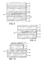
- FIG. 1 is a sectional view of one embodiment of a diode constructed according to the invention.
- FIGS. 2 , 3 , 4 , 5 , 6 , 7 , 8 , 9 , and 10 are sectional views illustrating the steps in a process of fabricating a diode according to the invention
- FIGS. 11 and 12 are graphs depicting the performance measured for diodes constructed according to the invention.
- FIGS. 13 and 14 are sectional views, analogous to FIG. 1 , depicting alternative embodiments of diodes constructed according to the invention.
- This invention provides rectifier diodes with very low forward voltage (V f ) values, for use in applications such as high efficiency power supplies, as well as other applications such as low voltage switching power supplies and power converters.
- a method according to the present invention provides full-wafer bonding of gallium nitride devices on a SiC substrate with front-side processing completed, to a metalized wafer carrier wafer.
- the SiC substrate is removed and ohmic contacts are places directly on the n+ GaN epitaxial layer. This eliminates the GaN—SiC interface barrier/resistance path as well as the SiC substrate resistance path. This helps minimize or reduce the parasitic resistive voltage drops.
- Embodiments of the invention are described herein with reference to cross-sectional view illustrations that are schematic illustrations of idealized embodiments of the invention. As such, variations from the shapes of the illustrations as a result, for example, of manufacturing techniques and/or tolerances are expected. Embodiments of the invention should not be construed as limited to the particular shapes of the regions illustrated herein but are to include deviations in shapes that result, for example, from manufacturing. A region illustrated or described as square or rectangular will typically have rounded or curved features due to normal manufacturing tolerances. Thus, the regions illustrated in the figures are schematic in nature and their shapes are not intended to illustrate the precise shape of a region of a device and are not intended to limit the scope of the invention.
- FIG. 1 shows one embodiment of a Schottky diode 100 constructed in accordance with the present invention that can be fabricated from many different material systems.
- the diode 100 is shown as a single device for ease of description and understanding, but as further described below, the diodes 100 are typically fabricated at a wafer level and then singulated from the wafer into individual devices. Thousands of devices are typically fabricated from a single wafer level process.
- the preferred diode 100 is fabricated using the Group-III nitride based material system.
- Group-III nitrides include the semiconductor compounds formed between nitrogen and the elements in Group-III of the periodic table, usually aluminum (Al), gallium (Ga), and indium (In). This group also includes ternary and tertiary compounds such as AlGaN and AlInGaN.
- the preferred materials for the diode are GaN and AlGaN.
- the diode 100 includes a substrate 102 of conductive material, that can be made of different materials but is preferable metallized silicon (Si) that acts as a conductive support layer for the device.
- a metal bonding layer 104 connects the support layer 102 to a Schottky metal layer 106 .
- a semiconducting AlGaN barrier layer 108 is disposed on the Schottky layer opposite the bonding layer, with an n ⁇ semiconducting GaN layer 110 disposed on the barrier layer.
- An n+ semiconducting GaN buffer layer 112 is disposed on the n ⁇ layer.
- an ohmic contact 114 which provides an electrical connection to the diode through the layer 112 , is disposed on the layer 112 .
- FIGS. 2-10 One method of making the diode depicted in FIG. 1 is shown in FIGS. 2-10 , and the method is described herein with reference to a single device with the understanding that the method is equally applicable to fabricated devices at the wafer level. The method is described with reference to certain materials having particular compositions, but it is understood that different materials can used having different compositions.
- the substrate 118 is preferably silicon carbide (SiC), however, which has a much closer crystal lattice match to Group III nitrides than sapphire and results in Group III nitride films of higher quality.
- SiC substrates are available from Cree Research, Inc., of Durham, N.C. and methods for producing them are set forth in the scientific literature, as well as in, e.g., U.S. Pat. Nos. Re. 34,861; 4,946,547; and 5,200,022.
- an n+ semiconducting buffer layer 112 is deposited on the nucleation layer 116 .
- the buffer layer is preferably GaN between 0.5 and 5 ⁇ m thick, doped with an impurity concentration of between 5 ⁇ 10 17 /cm 3 and 5 ⁇ 10 19 /cm 3 .
- an n ⁇ semiconducting layer 110 is then deposited on the buffer layer 112 , with the layer 110 preferably being formed of GaN between 0.5 and 5 ⁇ m thick, doped with an impurity concentration of between 1 ⁇ 10 15 /cm 3 and 1 ⁇ 10 17 /cm 3 .
- the barrier layer 108 is preferably 5 ⁇ thick and with a composition within the range of 15 ⁇ x ⁇ 45.
- the n+, n ⁇ and barrier layers may be deposited by deposition techniques known in the semiconductor fabrication art, including, e.g., metal-organic chemical vapor deposition (MOCVD).
- an SiO 2 dielectric layer 120 is deposited on the barrier layer 108 , then, as shown in FIG. 7 , a portion of the dielectric layer is removed and a Schottky metal 106 is deposited in the void remaining after the portion has been removed, so that the Schottky metal is in electrical contact with the barrier layer 108 .
- Standard metallization techniques as known in the art of semiconductor fabrication, can be used to form the Schottky metal, which is preferably Cr, although other metals could be used to achieve a low barrier height, the preferred materials being Cr, Fe, Mn, Nb, Ni, NiCr, Sn, Ta, Ti, Ge, and W.
- Schottky metals with different work functions result in different barrier potentials.
- Cr provides an acceptable barrier potential for a diode with Vf of around 0.2 v and is easy to deposit by conventional methods.
- the metal should be chosen to provide a low Schottky barrier potential and low V f , but high enough so that the reverse current remains low. If the metal chosen, for example, had a work function equal to the semiconductor's electron affinity, the barrier potential would approach zero (except in the case of a tunnel diode), resulting in a V f that approaches zero and also increases the diode's reverse current, such that the diode would become ohmic in nature and provide no rectification.
- the dielectric layer 120 is used as a protective layer and can be removed selectively at various points in the process.
- the Schottky metal could be deposited in a complete layer, then etched off later to define the Schottky barrier contact.
- the structure is flipped over and the dielectric layer/Schottky metal is bonded to a metallized Si conductive support layer 102 by means of a metal bonding layer 104 , preferably utilizing an Au—Sn utectic wafer bonding process.
- the bonding layer is thick metal, which exhibits a higher coefficient of thermal expansion than Si. Consequently, when a bonded wafer cools after the bonding process, this difference in thermal expansion may cause tensile stress in the bonding layer.
- the substrate 118 is later removed, as described below, the tensile stress in the bonding layer may cause the support layer 102 and the remaining layers to bow. This distortion in the layers is undesirable for subsequent fabrication steps, particularly those involving photolithography.
- the tensile stress effect can be ameliorated by adding an optional backside bonding layer 122 to the backside of the layer 104 (the backside bonding layer should be contacted by a nonmetallic surface during the bond process, to ensure that it adheres only to the support layer 102 , and not to the bond tool). With the additional bond layer, tensile stress is introduced in both bonding layers upon cool down. The stress in the backside bonding layer counteracts the stress introduced by the bond layer 102 to minimize the bowing after the removal of the substrate 118 .
- the SiC substrate 118 and the nucleating layer 116 are thinned and removed, and different removal methods can be used according to the present invention.
- most of the SiC substrate is removed by grinding, leaving only a remaining thin layer (e.g. 10-30 micron) that can be removed by reactive ion etching or other dry etching like Inductively Coupled Plasma Etching (ICP).
- ICP Inductively Coupled Plasma Etching
- n+, n ⁇ , and barrier layers are then removed to form a mesa diode structure on the SiO 2 dielectric layer 120 over the Schottky metal 106 .
- the removal can be accomplished by a number of etching techniques known in the semiconductor fabrication art, including, e.g., chemical etching, reactive ion etching (RIE), and ion mill etching.
- RIE reactive ion etching
- an ohmic contact 114 is deposited on the n+ layer 112 to complete the diode.
- Low voltage diodes were fabricated by the method above, with a 2 ⁇ m thick n+ layer doped to 1 ⁇ 10 16 /cm 3 , a 1 ⁇ m thick n ⁇ layer doped to 1 ⁇ 10 16 /cm 3 , and a thin 5 ⁇ barrier layer of approximate composition Al 0.3 Ga 0.7 N. An Al/Au ohmic contact was used. Standard dicing techniques were performed to obtain individual devices.
- FIG. 11 which is a plot of forward current I f (A/cm 2 ) on the vertical axis versus forward voltage V f (V) on the horizontal axis, as well as Table 1 below, display the performance exhibited by these devices.
- This diode structure exhibits minimal parasitic resistance. Besides yielding a low V f , these diode may be operable at a current density of greater than 100 A/cm 2 , hence improving capacitance per unit amperage.
- these devices began to show the impact of current spreading, because the total metal thickness for the ohmic contact was less than 0.5 ⁇ m. Metal thickening, to increase the ohmic metal to greater than 2 ⁇ m, should ameliorate this issue. Because of the low intrinsic barrier for these devices, they could be operated at a high forward current of 200 A/cm 2 , thereby gaining a capacitance advantage.
- FIG. 12 is a plot of forward current (I f ) on the vertical axis versus forward voltage (V f ) on the horizontal axis.
- the diode of the invention can also be made in alternative embodiments. Instead of complete removal of the substrate, for example, a via can be etched in the substrate to remove the material under the active device and to retain the remainder of the substrate material for mechanical support.
- a diode 200 made according to this second embodiment, is depicted in FIG. 13 , which is similar to FIG. 1 .
- the diode 200 is fabricated in a manner similar to the process described in conjunction with FIGS. 2 through 7 .
- a nucleation layer 216 is deposited on a SiC substrate 218 , then an n+ semiconducting buffer layer 212 is deposited on the nucleation layer.
- n ⁇ semiconducting layer 210 is deposited on the buffer layer 212 and a semiconducting barrier layer 208 is deposited on the n ⁇ layer 210 .
- a Schottky metal layer 206 is deposited on the barrier layer 208 .
- n+, n ⁇ , and buffer layers are then removed to form a mesa diode structure under the Schottky metal.
- a portion of the substrate 218 and the nucleation layer 216 is removed under the mesa diode structure to form a via, then an ohmic contact layer 214 is deposited on the substrate and in the via, such that the ohmic contact layer electrically connects with the n+ layer 212 .
- a third embodiment of the diode can be implemented on a bulk GaN wafer, with the bulk GaN wafer being subsequently thinned to reduce parasitic substrate resistance.
- the bulk GaN wafer does not need to be completely removed since there is no heterostructure epi-substrate interface, as with the GaN diode fabricated on a SiC substrate.
- reduction of substrate parasitic will be a function of the extent of thinning of the GaN substrate wafer.
- the third embodiment is shown as the diode 300 , as depicted in FIG. 14 , which is also similar to FIG. 1 .
- This embodiment like the second embodiment, is fabricated using a process similar to that described in conjunction with FIGS. 2 through 7 .
- a nucleation layer 316 is deposited on a GaN substrate 318 , then an n+ semiconducting buffer layer 312 is deposited on the nucleation layer.
- An n ⁇ semiconducting layer 310 is deposited on the buffer layer 312 and a semiconducting barrier layer 308 is deposited on the n ⁇ layer 310 .
- a Schottky metal layer 306 is deposited on the barrier layer 308 .
- n+, n ⁇ , and buffer layers are then removed to form a mesa diode structure under the Schottky metal.
- the GaN substrate 318 is thinned sufficiently to reduce parasitic resistance associated with the substrate, then an ohmic contact layer 314 is deposited on the substrate.
Abstract
A method of making a diode begins by depositing an AlxGa1-xN nucleation layer on a SiC substrate, then depositing an n+ GaN buffer layer, an n− GaN layer, an AlxGa1-xN barrier layer, and an SiO2 dielectric layer. A portion of the dielectric layer is removed and a Schottky metal deposited in the void. The dielectric layer is affixed to the support layer with a metal bonding layer using an Au—Sn utectic wafer bonding process, the substrate is removed using reactive ion etching to expose the n+ layer, selected portions of the n+, n−, and barrier layers are removed to form a mesa diode structure on the dielectric layer over the Schottky metal, and an ohmic contact is deposited on the n+ layer.
Description
This application is a divisional from, and claims the benefit of, U.S. patent application Ser. No. 11/655,696, filed Jan. 19, 2007, now U.S. Pat. No. 7,834,367 to Parikh et al., having the same title as the present application.
This invention was made with Government support under DARPA Contract No. 4400129974 (as subcontractor—Raytheon as prime). The Government has certain rights in this invention
This invention is concerned with diodes, and more particularly diodes exhibiting low on-state forward voltage and reduced parasitic resistance.
A diode is an electronic component that restricts the direction of movement of charge carriers. The diode essentially allows an electric current to flow in one direction, but substantially blocks current flow in the opposite direction.
Diode rectifiers are one of the most widely used devices in low voltage switching, power supplies, power converters and related applications. For efficient operation, it is desirable for such diodes to operate with low on-state voltage (a forward voltage drop Vf of 0.1-0.4V or lower), low reverse leakage current, a voltage blocking capability of 20-30V, and high switching speed. These features are important to achieve high conversion efficiency, which is the final goal of any rectifier for low voltage applications.
The most common diodes are based on semiconductor pn-junctions, typically using silicon (Si), with impurity elements introduced to modify, in a controlled manner, the diode's operating characteristics. Diodes can also be formed from other semiconductor materials, such as gallium arsenide (GaAs) and silicon carbide (SiC). In a pn diode, conventional current can flow from the p-type side (the anode) to the n-type side (the cathode), but not in the opposite direction.
A semiconductor diode's current-voltage, or I-V, characteristic curve is attributable to the depletion layer or depletion zone that exists at the pn junction between the differing semiconductor layers. When a pn junction is first created, conduction band (mobile) electrons from the n-doped region diffuse into the p-doped region, where there is a large population of holes (locations for electrons where no electron is present) with which the electrons can “recombine”. When a mobile electron recombines with a hole, the hole vanishes and the electron is no longer mobile, i.e., two charge carriers are eliminated. The region around the p-n junction becomes depleted of charge carriers and thus behaves as an insulator.
The width of the depletion zone, however, cannot grow without limit. For each electron-hole pair that recombines, a positively charged dopant ion is left behind in the n-doped region and a negatively charged dopant ion is left behind in the p-doped region. As recombination proceeds and more ions are created, an increasing electric field develops through the depletion zone, which acts to slow and then eventually stop recombination. At this point, there is a ‘built-in’ potential across the depletion zone.
If an external voltage is placed across the diode with the same polarity as the built-in potential, the depletion zone continues to act as an insulator, preventing any significant electric current. This is the reverse bias phenomenon. If the polarity of the external voltage opposes the built-in potential, however, recombination can once again proceed, resulting in substantial electric current through the p-n junction. For silicon diodes, the built-in potential is approximately 0.6 V. Thus, if an external current is passed through the diode, about 0.6 V will be developed across the diode, causing the p-doped region to be positive with respect to the n-doped region. The diode is said to be ‘turned on’, as it has a forward bias.
A diode's I-V characteristic can be approximated by two regions of operation. Below a certain difference is potential between the two leads attached to the diode, the depletion layer has significant width, and the diode can be thought of as an open (non-conductive) circuit. As the potential difference is increased, at some point the diode will become conductive and allow charges to flow. The diode can then be considered as a circuit element with zero (or at least very low) resistance. In a normal silicon diode at rated currents, the voltage drop across a conducting diode is approximately 0.6 to 0.7 volts.
In the reverse bias region for a normal p-n rectifier diode, the current through the device is very low (in the μA range) for all reverse voltages up to a point called the peak inverse voltage (PIV). Beyond this point, a process called reverse breakdown occurs, which causes the device to be damaged, accompanied by a large increase in current.
One disadvantage of a junction diode is that, during forward conduction, the power loss in the diode can become excessive for large current flow. Another type of diode, the Schottky barrier diode, utilizes a rectifying metal-to-semiconductor barrier instead of a pn junction. The junction between the metal and the semiconductor establishes a barrier region that, when properly fabricated, will minimize charge storage effects and improve the switching performance of the diode by shortening its turn-off time. [L. P. Hunter, Physics of Semiconductor Materials, Devices, and Circuits, Semiconductor Devices, Page 1-10 (1970)].
Common Schottky diodes have a lower forward voltage drop than pn-junction diodes and are thus more desirable in applications where energy losses in the diode can have a significant negative impact on the performance of the system, e.g., where diodes are used as output rectifiers in a switching power supply. For such applications, it is highly desirable to provide a rectifier with a very low forward voltage drop (0.1-0.4V), reduced reverse leakage current, low voltage blocking capability (20-30V), and high switching speed. These features are important to achieve high conversion efficiency, which is the final goal of any rectifier that is to be used for low voltage applications.
Schottky diodes can be used as low loss rectifiers, although their reverse leakage current is generally much higher than other rectifier designs. Schottky diodes are majority carrier devices; as such, they do not suffer from minority carrier storage problems that slow down most normal diodes. They also tend to have much lower junction capacitance than pn diodes, which contributes to their high switching speed.
One way to reduce the on-state voltage below 0.5V in a conventional Schottky diode is to reduce the diode's surface barrier potential. Reducing the barrier potential, however, results in a tradeoff of increased reverse leakage current. In addition, the reduced barrier can degrade high temperature operation and result in soft breakdown characteristics under reverse bias operation.
In addition, for Schottky diodes that are made of GaAs; one disadvantage of this material is that the Fermi level (or surface potential) is fixed or pinned at approximately 0.7 volts. (Si Schottky diodes also have this limitation to a certain extent.) As a result, the on-state forward voltage (Vf) is fixed. Regardless of the type of metal used to contact the semiconductor, the surface potential in such a diode cannot be lowered to lower Vf.
One solution to this limitation with GaAs is the gallium nitride (GaN) material system. GaN has a 3.4 eV wide direct bandgap, high electron velocity (2×107 cm/s), high breakdown fields (2×10⁶ V/cm) and the availability of heterostructures. GaN based low voltage diodes can achieve reduced forward voltage drops in comparison with conventional Schottky diode rectifiers (See, e.g., Parikh, et al., Gallium Nitride Based Diodes with Low Forward voltage and Low Reverse Current Operation, U.S. patent application Ser. No. 10/445,130, filed May 20, 2003, which is commonly assigned and the specification of which is incorporated herein by reference as if described in its entirety).
GaN low voltage diodes, however, can be typically fabricated on a SiC or GaN substrate. For a vertical diode device, the substrate is in the conductive path and contributes to the voltage drops. With typical substrate resistivity values of around 20-30 mohm-cm for SiC/GaN substrates, a 200 μm thick substrate will add 40-60 mV of voltage drop at an operating current density of 100 A/cm2. This additional voltage drop is unacceptable, since the target for total voltage drop at operating current is <200 mV. Furthermore, for the most commonly used SiC substrate (GaN substrates are expensive and small in diameter), an additional barrier is encountered at the GaN epi-SiC substrate interface. While there are techniques used to mitigate this barrier, they add extra complexity and may also contribute to increased resistance.
Consequently, a need has developed in the art for diodes that can be operated with lower forward voltage drops.
This invention provides a semiconductor diode structure and method for fabrication a diode structure that substantially reduces parasitic resistance in the diode and eliminates the associated resistive voltage drops.
A method of making a diode involves depositing an n+ semiconducting buffer layer on a substrate, depositing an n− semiconducting layer on the n+ layer, depositing a semiconducting barrier layer on the n− layer, and depositing a dielectric layer on the barrier layer. A portion of the dielectric layer is then removed, and a Schottky metal is deposited on the barrier layer in the void left by the removed portion. The dielectric layer and the Schottky metal are affixed to a conductive support layer with a metal bonding layer, the substrate is removed to expose the n+ layer, portions of the n+, n−, and barrier layers are selectively removed to form a mesa diode structure on the dielectric layer over the Schottky metal; and an ohmic contact is deposited on the n+ layer.
A second method of making a diode, is similar to the first, except that, after depositing a Schottky metal on the barrier layer, selective portions of the n+ and n− layers are removed to form a mesa diode structure under the Schottky metal, the substrate is removed under the mesa diode structure to form a via, and an ohmic contact is deposited on the n+ layer in the via.
A third method of making a diode is similar to the second method, except that the substrate is a GaN substrate and that, after selective portions of the n+ and n− layers are removed to form a mesa diode structure, the GaN substrate is thinned to reduce parasitic substrate resistance and the ohmic contact is deposited on the thinned substrate.
In more particular embodiments, the n+ layer, the n− layer, and the barrier layer comprise Group III nitrides. A nucleation layer may be deposited on the substrate, prior to depositing the n+ layer on the substrate. The nucleation layer may be AlxGa1-xN, and the n+ layer may be n+ doped GaN, particularly, a layer of GaN between 0.5 and 5 μm thick and doped with an impurity concentration of between 5×10¹⁷/cm3 and 5×10¹⁹/cm3.
The n− layer may be n− doped GaN, particularly, a layer of GaN between 0.5 and 5 μm thick and doped with an impurity concentration of between 1×10¹⁵/cm3 and 1×10¹⁷/cm3. The barrier layer may be AlGaN, particularly a layer with 30% Al for the AlxGa1-xN with 15≦x≦45. The thickness of the barrier layer may be between 0-30 A, particularly 5 A. The dielectric layer may be a SiO2 dielectric layer. The Schottky metal may be selected from the group consisting of Cr, Ge, Fe, Mn, Nb, Ni, NiCr, Sn, Ta, Ti, and W, preferably Cr.
The conductive support layer may be metallized Si, while the dielectric layer may be affixed to the support layer with a metal bonding layer using an Au—Sn Eutectic wafer bonding process. The ohmic contact material may be selected from the group consisting of Al/Au and Ti/Au or other suitable ohmic contacts to n+ GaN. Removing the substrate to expose the n+ layer may be accomplished using reactive ion etching. After affixing the dielectric layer to the support layer with a metal bonding layer, a backside bonding layer may be affixed to the support layer opposite the dielectric layer.
This invention provides rectifier diodes with very low forward voltage (Vf) values, for use in applications such as high efficiency power supplies, as well as other applications such as low voltage switching power supplies and power converters.
In one embodiment of a method according to the present invention provides full-wafer bonding of gallium nitride devices on a SiC substrate with front-side processing completed, to a metalized wafer carrier wafer. The SiC substrate is removed and ohmic contacts are places directly on the n+ GaN epitaxial layer. This eliminates the GaN—SiC interface barrier/resistance path as well as the SiC substrate resistance path. This helps minimize or reduce the parasitic resistive voltage drops.
It is also understood that when an element such as a layer, region or substrate is referred to as being “on” another element, it can be directly on the other element or intervening elements may also be present. Furthermore, relative terms such as “inner”, “outer”, “upper”, “above”, “lower”, “beneath”, and “below”, and similar terms, may be used herein to describe a relationship of one layer or another region. It is understood that these terms are intended to encompass different orientations of the device in addition to the orientation depicted in the figures.
Embodiments of the invention are described herein with reference to cross-sectional view illustrations that are schematic illustrations of idealized embodiments of the invention. As such, variations from the shapes of the illustrations as a result, for example, of manufacturing techniques and/or tolerances are expected. Embodiments of the invention should not be construed as limited to the particular shapes of the regions illustrated herein but are to include deviations in shapes that result, for example, from manufacturing. A region illustrated or described as square or rectangular will typically have rounded or curved features due to normal manufacturing tolerances. Thus, the regions illustrated in the figures are schematic in nature and their shapes are not intended to illustrate the precise shape of a region of a device and are not intended to limit the scope of the invention.
The preferred diode 100 is fabricated using the Group-III nitride based material system. Group-III nitrides include the semiconductor compounds formed between nitrogen and the elements in Group-III of the periodic table, usually aluminum (Al), gallium (Ga), and indium (In). This group also includes ternary and tertiary compounds such as AlGaN and AlInGaN. The preferred materials for the diode are GaN and AlGaN.
The diode 100 includes a substrate 102 of conductive material, that can be made of different materials but is preferable metallized silicon (Si) that acts as a conductive support layer for the device. A metal bonding layer 104 connects the support layer 102 to a Schottky metal layer 106. A semiconducting AlGaN barrier layer 108 is disposed on the Schottky layer opposite the bonding layer, with an n− semiconducting GaN layer 110 disposed on the barrier layer. An n+ semiconducting GaN buffer layer 112 is disposed on the n− layer. Finally, an ohmic contact 114, which provides an electrical connection to the diode through the layer 112, is disposed on the layer 112.
One method of making the diode depicted in FIG. 1 is shown in FIGS. 2-10 , and the method is described herein with reference to a single device with the understanding that the method is equally applicable to fabricated devices at the wafer level. The method is described with reference to certain materials having particular compositions, but it is understood that different materials can used having different compositions.
The method begins, as depicted in FIG. 2 , with the deposition of an AlxGa1-x N nucleation layer 116 on a substrate 118, with the AlN composition (i.e., x=1) being preferred for the nucleation layer 116. A variety of materials for the substrate 118, such as silicon, sapphire and silicon carbide, can be used for the substrate. The substrate 118 is preferably silicon carbide (SiC), however, which has a much closer crystal lattice match to Group III nitrides than sapphire and results in Group III nitride films of higher quality. SiC substrates are available from Cree Research, Inc., of Durham, N.C. and methods for producing them are set forth in the scientific literature, as well as in, e.g., U.S. Pat. Nos. Re. 34,861; 4,946,547; and 5,200,022.
Next, as shown in FIG. 3 , an n+ semiconducting buffer layer 112 is deposited on the nucleation layer 116. The buffer layer is preferably GaN between 0.5 and 5 μm thick, doped with an impurity concentration of between 5×10¹⁷/cm3 and 5×10¹⁹/cm3.
In FIG. 4 , an n− semiconducting layer 110 is then deposited on the buffer layer 112, with the layer 110 preferably being formed of GaN between 0.5 and 5 μm thick, doped with an impurity concentration of between 1×10¹⁵/cm3 and 1×10¹⁷/cm3.
A semiconducting barrier layer 108 of AlxGa1-xN, as shown in FIG. 5 , is deposited on the n− layer 110. The barrier layer 108 is preferably 5 Å thick and with a composition within the range of 15≦x≦45. The n+, n− and barrier layers may be deposited by deposition techniques known in the semiconductor fabrication art, including, e.g., metal-organic chemical vapor deposition (MOCVD).
Next, as depicted in FIG. 6 , an SiO2 dielectric layer 120 is deposited on the barrier layer 108, then, as shown in FIG. 7 , a portion of the dielectric layer is removed and a Schottky metal 106 is deposited in the void remaining after the portion has been removed, so that the Schottky metal is in electrical contact with the barrier layer 108. Standard metallization techniques, as known in the art of semiconductor fabrication, can be used to form the Schottky metal, which is preferably Cr, although other metals could be used to achieve a low barrier height, the preferred materials being Cr, Fe, Mn, Nb, Ni, NiCr, Sn, Ta, Ti, Ge, and W. Schottky metals with different work functions result in different barrier potentials. Cr provides an acceptable barrier potential for a diode with Vf of around 0.2 v and is easy to deposit by conventional methods.
The metal should be chosen to provide a low Schottky barrier potential and low Vf, but high enough so that the reverse current remains low. If the metal chosen, for example, had a work function equal to the semiconductor's electron affinity, the barrier potential would approach zero (except in the case of a tunnel diode), resulting in a Vf that approaches zero and also increases the diode's reverse current, such that the diode would become ohmic in nature and provide no rectification.
The dielectric layer 120 is used as a protective layer and can be removed selectively at various points in the process. Alternatively, the Schottky metal could be deposited in a complete layer, then etched off later to define the Schottky barrier contact.
At this point, as shown in FIG. 8 , the structure is flipped over and the dielectric layer/Schottky metal is bonded to a metallized Si conductive support layer 102 by means of a metal bonding layer 104, preferably utilizing an Au—Sn utectic wafer bonding process. The bonding layer is thick metal, which exhibits a higher coefficient of thermal expansion than Si. Consequently, when a bonded wafer cools after the bonding process, this difference in thermal expansion may cause tensile stress in the bonding layer. When the substrate 118 is later removed, as described below, the tensile stress in the bonding layer may cause the support layer 102 and the remaining layers to bow. This distortion in the layers is undesirable for subsequent fabrication steps, particularly those involving photolithography.
The tensile stress effect can be ameliorated by adding an optional backside bonding layer 122 to the backside of the layer 104 (the backside bonding layer should be contacted by a nonmetallic surface during the bond process, to ensure that it adheres only to the support layer 102, and not to the bond tool). With the additional bond layer, tensile stress is introduced in both bonding layers upon cool down. The stress in the backside bonding layer counteracts the stress introduced by the bond layer 102 to minimize the bowing after the removal of the substrate 118.
Next, as depicted in FIG. 9 , the SiC substrate 118 and the nucleating layer 116 are thinned and removed, and different removal methods can be used according to the present invention. In one embodiment most of the SiC substrate is removed by grinding, leaving only a remaining thin layer (e.g. 10-30 micron) that can be removed by reactive ion etching or other dry etching like Inductively Coupled Plasma Etching (ICP).
As shown in FIG. 10 , selected portions of the n+, n−, and barrier layers are then removed to form a mesa diode structure on the SiO2 dielectric layer 120 over the Schottky metal 106. The removal can be accomplished by a number of etching techniques known in the semiconductor fabrication art, including, e.g., chemical etching, reactive ion etching (RIE), and ion mill etching. Finally, an ohmic contact 114 is deposited on the n+ layer 112 to complete the diode.
Low voltage diodes were fabricated by the method above, with a 2 μm thick n+ layer doped to 1×10¹⁶/cm3, a 1 μm thick n− layer doped to 1×10¹⁶/cm3, and a thin 5 Å barrier layer of approximate composition Al0.3Ga0.7N. An Al/Au ohmic contact was used. Standard dicing techniques were performed to obtain individual devices.
| TABLE 1 | ||
| If (A/cm2) | Vf (V) | Vr (If/Ir = 100) |
| 100 | 0.15 | −3.31 |
| 200 | 0.18 | −7.77 |
This diode structure exhibits minimal parasitic resistance. Besides yielding a low Vf, these diode may be operable at a current density of greater than 100 A/cm2, hence improving capacitance per unit amperage. At the 1 A level, these devices began to show the impact of current spreading, because the total metal thickness for the ohmic contact was less than 0.5 μm. Metal thickening, to increase the ohmic metal to greater than 2 μm, should ameliorate this issue. Because of the low intrinsic barrier for these devices, they could be operated at a high forward current of 200 A/cm2, thereby gaining a capacitance advantage.
These devices were then packaged using standard Ag—Sn based die attachment techniques. The results for the packaged diodes are shown in FIG. 12 that, like FIG. 11 , is a plot of forward current (If) on the vertical axis versus forward voltage (Vf) on the horizontal axis.
The diode of the invention can also be made in alternative embodiments. Instead of complete removal of the substrate, for example, a via can be etched in the substrate to remove the material under the active device and to retain the remainder of the substrate material for mechanical support. A diode 200, made according to this second embodiment, is depicted in FIG. 13 , which is similar to FIG. 1 . The diode 200 is fabricated in a manner similar to the process described in conjunction with FIGS. 2 through 7 . A nucleation layer 216 is deposited on a SiC substrate 218, then an n+ semiconducting buffer layer 212 is deposited on the nucleation layer. An n− semiconducting layer 210 is deposited on the buffer layer 212 and a semiconducting barrier layer 208 is deposited on the n− layer 210. A Schottky metal layer 206 is deposited on the barrier layer 208.
Selected portions of the n+, n−, and buffer layers are then removed to form a mesa diode structure under the Schottky metal. Finally, a portion of the substrate 218 and the nucleation layer 216 is removed under the mesa diode structure to form a via, then an ohmic contact layer 214 is deposited on the substrate and in the via, such that the ohmic contact layer electrically connects with the n+ layer 212.
A third embodiment of the diode can be implemented on a bulk GaN wafer, with the bulk GaN wafer being subsequently thinned to reduce parasitic substrate resistance. The bulk GaN wafer does not need to be completely removed since there is no heterostructure epi-substrate interface, as with the GaN diode fabricated on a SiC substrate. Other than the elimination of this interfacial voltage drop, reduction of substrate parasitic will be a function of the extent of thinning of the GaN substrate wafer.
The third embodiment is shown as the diode 300, as depicted in FIG. 14 , which is also similar to FIG. 1 . This embodiment, like the second embodiment, is fabricated using a process similar to that described in conjunction with FIGS. 2 through 7 . A nucleation layer 316 is deposited on a GaN substrate 318, then an n+ semiconducting buffer layer 312 is deposited on the nucleation layer. An n− semiconducting layer 310 is deposited on the buffer layer 312 and a semiconducting barrier layer 308 is deposited on the n− layer 310. A Schottky metal layer 306 is deposited on the barrier layer 308.
Selected portions of the n+, n−, and buffer layers are then removed to form a mesa diode structure under the Schottky metal. The GaN substrate 318 is thinned sufficiently to reduce parasitic resistance associated with the substrate, then an ohmic contact layer 314 is deposited on the substrate.
The preferred embodiments of this invention have been illustrated and described above. Modifications and additional embodiments, however, will undoubtedly be apparent to those skilled in the art. Furthermore, equivalent elements may be substituted for those illustrated and described herein, parts or connections might be reversed or otherwise interchanged, and certain features of the invention may be utilized independently of other features. Consequently, the exemplary embodiments should be considered illustrative, rather than inclusive, while the appended claims are more indicative of the full scope of the invention.
Claims (17)
1. A diode, comprising:
a conductive support layer;
a Schottky metal layer on the conductive support layer;
a semiconducting barrier layer on the Schottky layer opposite the conductive support layer;
an n− semiconducting layer on the barrier layer opposite the Schottky layer;
an n+ semiconducting buffer layer on the n− layer opposite the barrier layer; and
an ohmic contact on the n+ layer opposite the n− layer.
2. The diode of claim 1 , further comprising a metal bonding layer affixing the Schottky layer to the support layer.
3. The diode of claim 1 , wherein the n+ layer, the n− layer, and the barrier layer comprises Group III nitrides.
4. The diode of claim 1 , wherein the Schottky metal is selected from the group consisting of Cr, Fe, Mn, Nb, Ni, NiCr, Sn, Ta, Ti, Ge, and W.
5. The diode of claim 2 , wherein the conductive support layer is metallized Si.
6. A diode, comprising:
a conductive support layer;
a Schottky metal layer;
a metal bonding layer affixing the Schottky layer to the support layer;
a 0-20 Å thick semiconducting barrier layer of AlxGa1-xN, with 0.15≦x≦0.45, disposed on the Schottky layer opposite the bonding layer;
an n− semiconducting layer of GaN, between 0.5 and 5 μm thick and doped with an impurity concentration of between 1×10¹⁵/cm3 and 1×10¹⁷/cm3, disposed on the barrier layer opposite the Schottky layer;
an n+ semiconducting buffer layer of GaN, between 0.5 and 5 μm thick and doped with an impurity concentration of between 5×10¹⁷/cm3 and 5×10¹⁹/cm3, disposed on the n− layer opposite the barrier layer; and
an ohmic contact disposed on the n+ layer opposite the n− layer.
7. The diode of claim 1 , exhibiting a Vf of approximately 0.2V.
8. The diode of claim 1 , exhibiting a Vf of less than 0.2V.
9. The diode of claim 1 , wherein said n+ semiconducting buffer layer of GaN is between 0.5 and 5 μm thick and doped with an impurity concentration of between 5×10¹⁷/cm3 and 5×10¹⁹/cm3.
10. The diode of claim 1 , wherein said n− semiconducting layer of GaN, is between 0.5 and 5 μm thick and doped with an impurity concentration of between 1×10¹⁵/cm3 and 1×10¹⁷/cm3.
11. The diode of claim 1 , wherein said semiconducting barrier layer comprises AlxGa1-xN and is between 0-20 Å thick, with 0.15≦x≦0.45.
12. The diode of claim 6 , wherein the Schottky metal comprises a material from the group consisting of Cr, Fe, Mn, Nb, Ni, NiCr, Sn, Ta, Ti, Ge, W and combinations thereof.
13. The diode of claim 6 , wherein the conductive support layer comprises a metallized layer.
14. The diode of claim 6 , wherein the conductive support layer is metallized Si.
15. The diode of claim 6 , exhibiting a Vf of approximately 0.2V.
16. The diode of claim 6 , exhibiting a Vf of less than 0.2V.
17. The diode of claim 1 , further comprising a bonding layer between the conductive support layer and the Schottky metal layer.
Priority Applications (2)
| Application Number | Priority Date | Filing Date | Title |
|---|---|---|---|
| US12/905,374 US8344398B2 (en) | 2007-01-19 | 2010-10-15 | Low voltage diode with reduced parasitic resistance and method for fabricating |
| US13/693,929 US9041139B2 (en) | 2007-01-19 | 2012-12-04 | Low voltage diode with reduced parasitic resistance and method for fabricating |
Applications Claiming Priority (2)
| Application Number | Priority Date | Filing Date | Title |
|---|---|---|---|
| US11/655,696 US7834367B2 (en) | 2007-01-19 | 2007-01-19 | Low voltage diode with reduced parasitic resistance and method for fabricating |
| US12/905,374 US8344398B2 (en) | 2007-01-19 | 2010-10-15 | Low voltage diode with reduced parasitic resistance and method for fabricating |
Related Parent Applications (1)
| Application Number | Title | Priority Date | Filing Date |
|---|---|---|---|
| US11/655,696 Division US7834367B2 (en) | 2007-01-19 | 2007-01-19 | Low voltage diode with reduced parasitic resistance and method for fabricating |
Related Child Applications (1)
| Application Number | Title | Priority Date | Filing Date |
|---|---|---|---|
| US13/693,929 Division US9041139B2 (en) | 2007-01-19 | 2012-12-04 | Low voltage diode with reduced parasitic resistance and method for fabricating |
Publications (2)
| Publication Number | Publication Date |
|---|---|
| US20110031579A1 US20110031579A1 (en) | 2011-02-10 |
| US8344398B2 true US8344398B2 (en) | 2013-01-01 |
Family
ID=39312953
Family Applications (3)
| Application Number | Title | Priority Date | Filing Date |
|---|---|---|---|
| US11/655,696 Active 2027-07-17 US7834367B2 (en) | 2007-01-19 | 2007-01-19 | Low voltage diode with reduced parasitic resistance and method for fabricating |
| US12/905,374 Active US8344398B2 (en) | 2007-01-19 | 2010-10-15 | Low voltage diode with reduced parasitic resistance and method for fabricating |
| US13/693,929 Active US9041139B2 (en) | 2007-01-19 | 2012-12-04 | Low voltage diode with reduced parasitic resistance and method for fabricating |
Family Applications Before (1)
| Application Number | Title | Priority Date | Filing Date |
|---|---|---|---|
| US11/655,696 Active 2027-07-17 US7834367B2 (en) | 2007-01-19 | 2007-01-19 | Low voltage diode with reduced parasitic resistance and method for fabricating |
Family Applications After (1)
| Application Number | Title | Priority Date | Filing Date |
|---|---|---|---|
| US13/693,929 Active US9041139B2 (en) | 2007-01-19 | 2012-12-04 | Low voltage diode with reduced parasitic resistance and method for fabricating |
Country Status (3)
| Country | Link |
|---|---|
| US (3) | US7834367B2 (en) |
| EP (1) | EP1947700B1 (en) |
| JP (1) | JP5011069B2 (en) |
Cited By (1)
| Publication number | Priority date | Publication date | Assignee | Title |
|---|---|---|---|---|
| US9502992B2 (en) | 2012-06-01 | 2016-11-22 | Coriant Operations, Inc. | Diode substitute with low drop and minimal loading |
Families Citing this family (21)
| Publication number | Priority date | Publication date | Assignee | Title |
|---|---|---|---|---|
| EP2111632A1 (en) * | 2007-02-12 | 2009-10-28 | The Regents of the University of California | Cleaved facet (ga,al,in)n edge-emitting laser diodes grown on semipolar {11-2n} bulk gallium nitride substrates |
| KR20090035869A (en) * | 2007-10-08 | 2009-04-13 | 삼성전자주식회사 | Organic semiconductor device |
| JP5506258B2 (en) * | 2008-08-06 | 2014-05-28 | キヤノン株式会社 | Rectifier element |
| US8766395B2 (en) | 2009-03-25 | 2014-07-01 | Qunano Ab | Schottky device |
| US9583678B2 (en) | 2009-09-18 | 2017-02-28 | Soraa, Inc. | High-performance LED fabrication |
| US8933644B2 (en) | 2009-09-18 | 2015-01-13 | Soraa, Inc. | LED lamps with improved quality of light |
| JP2013505588A (en) * | 2009-09-18 | 2013-02-14 | ソラア インコーポレーテッド | Power light emitting diode and method using current density manipulation |
| US9293644B2 (en) | 2009-09-18 | 2016-03-22 | Soraa, Inc. | Power light emitting diode and method with uniform current density operation |
| KR20120032258A (en) * | 2010-09-28 | 2012-04-05 | 삼성엘이디 주식회사 | Gallium nitride based semiconductor device and method of manufacturing the same |
| WO2013063038A1 (en) * | 2011-10-24 | 2013-05-02 | Rosestreet Labs, Llc | Nitride uv light sensors on silicon substrates |
| US8981432B2 (en) * | 2012-08-10 | 2015-03-17 | Avogy, Inc. | Method and system for gallium nitride electronic devices using engineered substrates |
| US9761763B2 (en) | 2012-12-21 | 2017-09-12 | Soraa, Inc. | Dense-luminescent-materials-coated violet LEDs |
| US9410664B2 (en) | 2013-08-29 | 2016-08-09 | Soraa, Inc. | Circadian friendly LED light source |
| CN103545405B (en) * | 2013-11-11 | 2016-03-30 | 天津三安光电有限公司 | Iii-nitride light emitting devices |
| JP6266490B2 (en) | 2014-11-04 | 2018-01-24 | エア・ウォーター株式会社 | Semiconductor device and manufacturing method thereof |
| CN108369964B (en) * | 2015-12-25 | 2021-09-10 | 出光兴产株式会社 | Laminated body |
| DE102016013542A1 (en) | 2016-11-14 | 2018-05-17 | 3 - 5 Power Electronics GmbH | Stacked Schottky diode |
| US10204778B2 (en) * | 2016-12-28 | 2019-02-12 | QROMIS, Inc. | Method and system for vertical power devices |
| JP2020038939A (en) * | 2018-09-05 | 2020-03-12 | トレックス・セミコンダクター株式会社 | Method for manufacturing vertical compound semiconductor device |
| CN110544719A (en) * | 2019-09-16 | 2019-12-06 | 河北工业大学 | GaN-based PIN diode device structure and preparation method thereof |
| CN114122106B (en) * | 2021-10-20 | 2024-04-05 | 苏州科技大学 | Schottky junction with continuously adjustable open-circuit voltage and preparation and application thereof |
Citations (92)
| Publication number | Priority date | Publication date | Assignee | Title |
|---|---|---|---|---|
| US3896479A (en) | 1973-09-24 | 1975-07-22 | Bell Telephone Labor Inc | Reduced stresses in iii-v semiconductor devices |
| US4152044A (en) | 1977-06-17 | 1979-05-01 | International Telephone And Telegraph Corporation | Galium aluminum arsenide graded index waveguide |
| FR2586844A1 (en) | 1985-08-27 | 1987-03-06 | Sofrela Sa | Signalling device using light-emitting diodes |
| US4675575A (en) | 1984-07-13 | 1987-06-23 | E & G Enterprises | Light-emitting diode assemblies and systems therefore |
| EP0272985A2 (en) | 1986-12-20 | 1988-06-29 | Fujitsu Limited | Constant current semiconductor device |
| JPS63288061A (en) | 1987-05-20 | 1988-11-25 | Fujitsu Ltd | Semiconductor negative resistance element |
| US4946547A (en) | 1989-10-13 | 1990-08-07 | Cree Research, Inc. | Method of preparing silicon carbide surfaces for crystal growth |
| JPH0575101A (en) | 1991-09-10 | 1993-03-26 | Sanken Electric Co Ltd | Semiconductor device having schottky barrier |
| US5200022A (en) | 1990-10-03 | 1993-04-06 | Cree Research, Inc. | Method of improving mechanically prepared substrate surfaces of alpha silicon carbide for deposition of beta silicon carbide thereon and resulting product |
| JPH05283672A (en) | 1992-03-30 | 1993-10-29 | Murata Mfg Co Ltd | Schottky barrier semiconductor device |
| JPH06268257A (en) | 1993-03-12 | 1994-09-22 | Nichia Chem Ind Ltd | Gallium nitride compound semiconductor light emitting element |
| USRE34861E (en) | 1987-10-26 | 1995-02-14 | North Carolina State University | Sublimation of silicon carbide to produce large, device quality single crystals of silicon carbide |
| JPH07162038A (en) | 1993-12-10 | 1995-06-23 | Nichia Chem Ind Ltd | Gallium nitride compound semiconductor light emitting diode |
| JPH07176826A (en) | 1993-12-17 | 1995-07-14 | Nichia Chem Ind Ltd | Gallium nitride compound semiconductor laser element |
| US5477436A (en) | 1992-08-29 | 1995-12-19 | Robert Bosch Gmbh | Illuminating device for motor vehicles |
| JPH0823124A (en) | 1994-07-06 | 1996-01-23 | Nichia Chem Ind Ltd | Light-emitting element of gallium nitride compound semiconductor |
| JPH0870139A (en) | 1994-06-24 | 1996-03-12 | Nichia Chem Ind Ltd | Method for crystal growth of n-type gallium nitride compound semiconductor |
| JPH08162671A (en) | 1994-10-07 | 1996-06-21 | Nichia Chem Ind Ltd | Nitride semiconductor light emitting diode |
| JPH08274414A (en) | 1995-01-31 | 1996-10-18 | Nichia Chem Ind Ltd | Nitride semiconductor laser element |
| US5612567A (en) | 1996-05-13 | 1997-03-18 | North Carolina State University | Schottky barrier rectifiers and methods of forming same |
| JPH09148678A (en) | 1995-11-24 | 1997-06-06 | Nichia Chem Ind Ltd | Nitride semiconductor light emitting element |
| JPH09153642A (en) | 1995-09-29 | 1997-06-10 | Nichia Chem Ind Ltd | Nitride semiconductor light emitting element |
| JPH09162444A (en) | 1995-12-11 | 1997-06-20 | Nichia Chem Ind Ltd | Nitride semiconductor multi-color light emitting device and its production |
| JPH09219556A (en) | 1995-11-24 | 1997-08-19 | Nichia Chem Ind Ltd | Nitride semiconductor laser element |
| JPH09330630A (en) | 1996-06-12 | 1997-12-22 | Nec Corp | Lighting switch |
| JPH1012969A (en) | 1996-06-19 | 1998-01-16 | Nichia Chem Ind Ltd | Nitride semiconductor laser element |
| JPH1033557A (en) | 1996-07-19 | 1998-02-10 | Matsushita Electric Ind Co Ltd | Dental gas laser system |
| JPH1041581A (en) | 1996-05-21 | 1998-02-13 | Nichia Chem Ind Ltd | Nitride semiconductor element |
| JPH1065271A (en) | 1996-08-13 | 1998-03-06 | Toshiba Corp | Gallium nitride based semiconductor light-emitting element |
| JPH10145000A (en) | 1996-11-07 | 1998-05-29 | Nichia Chem Ind Ltd | Nitride semiconductor element and its manufacture |
| JPH10145002A (en) | 1996-11-15 | 1998-05-29 | Nichia Chem Ind Ltd | Nitride semiconductor device and method for growing the nitride semiconductor |
| WO1998031055A1 (en) | 1997-01-09 | 1998-07-16 | Nichia Chemical Industries, Ltd. | Nitride semiconductor device |
| FR2759188A1 (en) | 1997-01-31 | 1998-08-07 | Thery Hindrick | Signal light used for controlling road traffic |
| WO1998037585A1 (en) | 1997-02-24 | 1998-08-27 | Minnesota Mining And Manufacturing Company | Passivation capping layer for ohmic contact in ii-vi semiconductor light transducing device |
| EP0881666A2 (en) | 1997-05-26 | 1998-12-02 | Sony Corporation | P-type nitrogen compound semiconductor and method of manufacturing same |
| WO1998056043A1 (en) | 1997-06-03 | 1998-12-10 | Daimlerchrysler Ag | Semiconductor component and method for producing the same |
| WO1999005728A1 (en) | 1997-07-25 | 1999-02-04 | Nichia Chemical Industries, Ltd. | Nitride semiconductor device |
| JPH1140850A (en) | 1997-07-23 | 1999-02-12 | Toyoda Gosei Co Ltd | Manufacture of iii nitride compound semiconductor element |
| JPH1174562A (en) | 1997-06-30 | 1999-03-16 | Nichia Chem Ind Ltd | Nitride semiconductor element |
| JPH11186659A (en) | 1997-12-22 | 1999-07-09 | Nichia Chem Ind Ltd | Nitride semiconductor laser element |
| JPH11191638A (en) | 1997-10-01 | 1999-07-13 | Nichia Chem Ind Ltd | Nitride semiconductor device |
| JPH11224972A (en) | 1995-11-24 | 1999-08-17 | Nichia Chem Ind Ltd | Nitride semiconductor light-emitting element |
| EP0936682A1 (en) | 1996-07-29 | 1999-08-18 | Nichia Chemical Industries, Ltd. | Light emitting device and display device |
| JPH11238945A (en) | 1997-12-18 | 1999-08-31 | Nichia Chem Ind Ltd | Nitride semiconductor light-emitting device |
| WO1999046822A1 (en) | 1998-03-12 | 1999-09-16 | Nichia Chemical Industries, Ltd. | Nitride semiconductor device |
| JPH11251684A (en) | 1998-02-26 | 1999-09-17 | Nichia Chem Ind Ltd | Nitride semiconductor element |
| JPH11298090A (en) | 1998-04-09 | 1999-10-29 | Nichia Chem Ind Ltd | Nitride semiconductor element |
| JPH11330552A (en) | 1998-05-18 | 1999-11-30 | Nichia Chem Ind Ltd | Nitride semiconductor light-emitting element and light-emitting device |
| JP2000049363A (en) | 1998-07-31 | 2000-02-18 | Denso Corp | Schottky diode and its manufacture |
| JP2000068594A (en) | 1997-09-01 | 2000-03-03 | Nichia Chem Ind Ltd | Nitride semiconductor element |
| US6046464A (en) | 1995-03-29 | 2000-04-04 | North Carolina State University | Integrated heterostructures of group III-V nitride semiconductor materials including epitaxial ohmic contact comprising multiple quantum well |
| JP2000133883A (en) | 1998-10-22 | 2000-05-12 | Nichia Chem Ind Ltd | Nitride semiconductor element |
| JP2000150920A (en) | 1998-11-12 | 2000-05-30 | Nippon Telegr & Teleph Corp <Ntt> | Manufacture of schottky junction semiconductor diode device |
| JP2000150956A (en) | 1998-11-18 | 2000-05-30 | Nichia Chem Ind Ltd | Nitride semiconductor light emitting element |
| JP2000244072A (en) | 1998-10-06 | 2000-09-08 | Nichia Chem Ind Ltd | Nitride semiconductor element |
| JP2000307149A (en) | 1999-04-21 | 2000-11-02 | Nichia Chem Ind Ltd | Nitride semiconductor element |
| WO2000076004A1 (en) | 1999-06-07 | 2000-12-14 | Nichia Corporation | Nitride semiconductor device |
| JP2001168471A (en) | 1998-12-15 | 2001-06-22 | Nichia Chem Ind Ltd | Nitride semiconductor light-emitting element |
| US6330111B1 (en) | 2000-06-13 | 2001-12-11 | Kenneth J. Myers, Edward Greenberg | Lighting elements including light emitting diodes, microprism sheet, reflector, and diffusing agent |
| US6331915B1 (en) | 2000-06-13 | 2001-12-18 | Kenneth J. Myers | Lighting element including light emitting diodes, microprism sheet, reflector, and diffusing agent |
| WO2002005399A1 (en) | 2000-07-07 | 2002-01-17 | Nichia Corporation | Nitride semiconductor device |
| US20020015013A1 (en) | 2000-06-28 | 2002-02-07 | Larry Ragle | Integrated color LED chip |
| FR2814220A1 (en) | 2000-09-18 | 2002-03-22 | Koito Mfg Co Ltd | VEHICLE LAMP COMPRISING SEVERAL PHOTOEMISSIVE DIODES |
| US20020054495A1 (en) | 2000-09-18 | 2002-05-09 | Koito Manufacturing Co., Ltd. | Vehicle lamp |
| US20030015708A1 (en) | 2001-07-23 | 2003-01-23 | Primit Parikh | Gallium nitride based diodes with low forward voltage and low reverse current operation |
| US20030020069A1 (en) | 2001-07-25 | 2003-01-30 | Motorola, Inc. | Structure and method for optimizing transmission media through dielectric layering and doping in semiconductor structures and devices utilizing the formation of a compliant substrate |
| JP2003059938A (en) | 2001-06-07 | 2003-02-28 | Nippon Telegr & Teleph Corp <Ntt> | Nitride semiconductor stack and semiconductor device therefor |
| US20030085409A1 (en) | 2001-11-02 | 2003-05-08 | Yu-Chen Shen | Indium gallium nitride separate confinement heterostructure light emitting devices |
| US20030165169A1 (en) | 2002-03-01 | 2003-09-04 | Opnext Japan, Inc. | Semiconductor laser diode and optical module |
| EP1349202A2 (en) | 2002-03-28 | 2003-10-01 | Rohm Co., Ltd. | Semiconductor device and method of manufacturing the same |
| US6746889B1 (en) | 2001-03-27 | 2004-06-08 | Emcore Corporation | Optoelectronic device with improved light extraction |
| US6784463B2 (en) | 1997-06-03 | 2004-08-31 | Lumileds Lighting U.S., Llc | III-Phospide and III-Arsenide flip chip light-emitting devices |
| US20040207313A1 (en) | 2003-04-21 | 2004-10-21 | Sharp Kabushiki Kaisha | LED device and portable telephone, digital camera and LCD apparatus using the same |
| US20050077535A1 (en) | 2003-10-08 | 2005-04-14 | Joinscan Electronics Co., Ltd | LED and its manufacturing process |
| US20050117320A1 (en) | 2003-11-14 | 2005-06-02 | Hon Hai Precision Industry Co., Ltd. | Light-emitting diode and backlight system using the same |
| US20050152127A1 (en) | 2003-12-19 | 2005-07-14 | Takayuki Kamiya | LED lamp apparatus |
| US20050173692A1 (en) | 2002-12-27 | 2005-08-11 | Park Young H. | Vertical GaN light emitting diode and method for manufacturing the same |
| US20050173728A1 (en) | 2004-02-05 | 2005-08-11 | Saxler Adam W. | Nitride heterojunction transistors having charge-transfer induced energy barriers and methods of fabricating the same |
| US6932497B1 (en) | 2003-12-17 | 2005-08-23 | Jean-San Huang | Signal light and rear-view mirror arrangement |
| US20060034576A1 (en) | 2004-08-16 | 2006-02-16 | Merritt Scott A | Superluminescent diodes having high output power and reduced internal reflections |
| US20060081862A1 (en) | 2004-10-14 | 2006-04-20 | Chua Janet B Y | Device and method for emitting output light using quantum dots and non-quantum fluorescent material |
| EP1653255A2 (en) | 2004-10-29 | 2006-05-03 | Pentair Water Pool and Spa, Inc. | Selectable beam lens for underwater light |
| EP1681509A1 (en) | 2005-01-17 | 2006-07-19 | Omron Corporation | Luminescent light source and luminescent source array |
| US7087936B2 (en) | 2003-04-30 | 2006-08-08 | Cree, Inc. | Methods of forming light-emitting devices having an antireflective layer that has a graded index of refraction |
| US20060220046A1 (en) | 2005-03-04 | 2006-10-05 | Chuan-Pei Yu | Led |
| US20060267031A1 (en) | 2000-12-28 | 2006-11-30 | Stefan Tasch | Light source with a light-emitting element |
| US20070025231A1 (en) | 2005-07-29 | 2007-02-01 | Masanao Ochiai | Semiconductor laser device |
| JP2007036010A (en) | 2005-07-28 | 2007-02-08 | Toshiba Corp | Schottky barrier diode equipment and its manufacturing method |
| US20080036364A1 (en) | 2006-08-10 | 2008-02-14 | Intematix Corporation | Two-phase yellow phosphor with self-adjusting emission wavelength |
| US20080074032A1 (en) | 2004-04-19 | 2008-03-27 | Tadashi Yano | Method for Fabricating Led Illumination Light Source and Led Illumination Light Source |
| EP2048718A1 (en) | 2007-10-10 | 2009-04-15 | Cree, Inc. | Multiple conversion material light emitting diode package and method of fabricating same |
| US20110193057A1 (en) | 2007-11-30 | 2011-08-11 | Osram Opto Semiconductors Gmbh | LED Having Current Spreading Layer |
Family Cites Families (54)
| Publication number | Priority date | Publication date | Assignee | Title |
|---|---|---|---|---|
| US3886580A (en) * | 1973-10-09 | 1975-05-27 | Cutler Hammer Inc | Tantalum-gallium arsenide schottky barrier semiconductor device |
| JPH077180B2 (en) | 1985-12-12 | 1995-01-30 | コニカ株式会社 | Variable Copy Optical System |
| JPH03191447A (en) | 1989-12-21 | 1991-08-21 | Nec Corp | Decoding system |
| US5034783A (en) | 1990-07-27 | 1991-07-23 | At&T Bell Laboratories | Semiconductor device including cascadable polarization independent heterostructure |
| JP3191447B2 (en) | 1992-10-21 | 2001-07-23 | 株式会社ニコン | Method of manufacturing resin-bonded aspheric lens |
| US5705321A (en) | 1993-09-30 | 1998-01-06 | The University Of New Mexico | Method for manufacture of quantum sized periodic structures in Si materials |
| US6388272B1 (en) * | 1996-03-07 | 2002-05-14 | Caldus Semiconductor, Inc. | W/WC/TAC ohmic and rectifying contacts on SiC |
| JP3374737B2 (en) | 1997-01-09 | 2003-02-10 | 日亜化学工業株式会社 | Nitride semiconductor device |
| JP3985065B2 (en) | 1997-05-14 | 2007-10-03 | 忠弘 大見 | Porous silicon substrate forming method and porous silicon substrate forming apparatus |
| DE19729396A1 (en) | 1997-07-09 | 1999-01-14 | Siemens Ag | Electrical contact for a II-VI semiconductor device and method for producing the electrical contact |
| JP3744795B2 (en) | 1998-04-17 | 2006-02-15 | バルベリーニ ソシエタ ペル アチオニ | Plant and process for automatically bonding polarizing lenses |
| JP3559453B2 (en) | 1998-06-29 | 2004-09-02 | 株式会社東芝 | Light emitting element |
| WO2000021143A1 (en) | 1998-10-05 | 2000-04-13 | Osram Opto Semiconductors Gmbh & Co. Ohg | Radiation emitting semiconductor chip |
| US7001536B2 (en) | 1999-03-23 | 2006-02-21 | The Trustees Of Princeton University | Organometallic complexes as phosphorescent emitters in organic LEDs |
| DE19918370B4 (en) | 1999-04-22 | 2006-06-08 | Osram Opto Semiconductors Gmbh | LED white light source with lens |
| US6515313B1 (en) | 1999-12-02 | 2003-02-04 | Cree Lighting Company | High efficiency light emitters with reduced polarization-induced charges |
| TW465123B (en) | 2000-02-02 | 2001-11-21 | Ind Tech Res Inst | High power white light LED |
| US6447604B1 (en) | 2000-03-13 | 2002-09-10 | Advanced Technology Materials, Inc. | Method for achieving improved epitaxy quality (surface texture and defect density) on free-standing (aluminum, indium, gallium) nitride ((al,in,ga)n) substrates for opto-electronic and electronic devices |
| JP4406490B2 (en) | 2000-03-14 | 2010-01-27 | 株式会社朝日ラバー | Light emitting diode |
| US6765242B1 (en) | 2000-04-11 | 2004-07-20 | Sandia Corporation | Npn double heterostructure bipolar transistor with ingaasn base region |
| EP1277241B1 (en) | 2000-04-26 | 2017-12-13 | OSRAM Opto Semiconductors GmbH | Gan-based light-emitting-diode chip |
| JP2001332770A (en) | 2000-05-23 | 2001-11-30 | Koha Co Ltd | Resin-sealing method of led chip |
| US6504179B1 (en) | 2000-05-29 | 2003-01-07 | Patent-Treuhand-Gesellschaft Fur Elektrische Gluhlampen Mbh | Led-based white-emitting illumination unit |
| US6611002B2 (en) * | 2001-02-23 | 2003-08-26 | Nitronex Corporation | Gallium nitride material devices and methods including backside vias |
| JP3830083B2 (en) | 2001-03-07 | 2006-10-04 | スタンレー電気株式会社 | Semiconductor device and manufacturing method thereof |
| JP4210823B2 (en) * | 2001-08-20 | 2009-01-21 | サンケン電気株式会社 | Shiyaki barrier diode and manufacturing method thereof |
| WO2003035945A2 (en) | 2001-10-26 | 2003-05-01 | Ammono Sp. Zo.O. | Substrate for epitaxy |
| WO2003044870A1 (en) | 2001-11-22 | 2003-05-30 | Mireille Georges | Light-emitting diode illuminating optical device |
| US7470941B2 (en) | 2001-12-06 | 2008-12-30 | Hrl Laboratories, Llc | High power-low noise microwave GaN heterojunction field effect transistor |
| JP3802424B2 (en) | 2002-01-15 | 2006-07-26 | 株式会社東芝 | Semiconductor light emitting device and manufacturing method thereof |
| JP3782357B2 (en) | 2002-01-18 | 2006-06-07 | 株式会社東芝 | Manufacturing method of semiconductor light emitting device |
| JP3878868B2 (en) | 2002-03-01 | 2007-02-07 | シャープ株式会社 | GaN-based laser element |
| JP3801931B2 (en) | 2002-03-05 | 2006-07-26 | ローム株式会社 | Structure and manufacturing method of light emitting device using LED chip |
| EP1490453B1 (en) | 2002-03-25 | 2012-08-15 | Philips Intellectual Property & Standards GmbH | Tri-color white light led lamp |
| US7792170B2 (en) | 2002-09-20 | 2010-09-07 | Mitsubishi Chemical Corporation | Semiconductor laser |
| US6815241B2 (en) | 2002-09-25 | 2004-11-09 | Cao Group, Inc. | GaN structures having low dislocation density and methods of manufacture |
| US6693357B1 (en) | 2003-03-13 | 2004-02-17 | Texas Instruments Incorporated | Methods and semiconductor devices with wiring layer fill structures to improve planarization uniformity |
| JP4058627B2 (en) | 2003-03-14 | 2008-03-12 | 株式会社朝日ラバー | Manufacturing method of resin lens for semiconductor optical element |
| JP4182783B2 (en) | 2003-03-14 | 2008-11-19 | 豊田合成株式会社 | LED package |
| US20040183081A1 (en) | 2003-03-20 | 2004-09-23 | Alexander Shishov | Light emitting diode package with self dosing feature and methods of forming same |
| JP4030463B2 (en) | 2003-05-20 | 2008-01-09 | 三洋電機株式会社 | LED light source and manufacturing method thereof |
| EP1629537B1 (en) | 2003-05-30 | 2014-07-30 | OSRAM Opto Semiconductors GmbH | Light-emitting diode |
| US20050048766A1 (en) | 2003-08-31 | 2005-03-03 | Wen-Chieh Wu | Method for fabricating a conductive plug in integrated circuit |
| JP4590905B2 (en) | 2003-10-31 | 2010-12-01 | 豊田合成株式会社 | Light emitting element and light emitting device |
| US6943381B2 (en) | 2004-01-30 | 2005-09-13 | Lumileds Lighting U.S., Llc | III-nitride light-emitting devices with improved high-current efficiency |
| JP4233466B2 (en) | 2004-02-12 | 2009-03-04 | 三菱化学株式会社 | LIGHT EMITTING DEVICE, LIGHTING DEVICE, AND DISPLAY DEVICE |
| US7517728B2 (en) | 2004-03-31 | 2009-04-14 | Cree, Inc. | Semiconductor light emitting devices including a luminescent conversion element |
| JP4180017B2 (en) * | 2004-05-17 | 2008-11-12 | 三菱電機株式会社 | Schottky barrier diode |
| JP4567426B2 (en) * | 2004-11-25 | 2010-10-20 | パナソニック株式会社 | Schottky barrier diode and diode array |
| US7491626B2 (en) | 2005-06-20 | 2009-02-17 | Sensor Electronic Technology, Inc. | Layer growth using metal film and/or islands |
| EP1902466A4 (en) * | 2005-07-05 | 2010-09-08 | Int Rectifier Corp | Schottky diode with improved surge capability |
| KR101332139B1 (en) | 2005-12-21 | 2013-11-21 | 크리, 인코포레이티드 | Lighting device and lighting method |
| WO2007121486A2 (en) | 2006-04-18 | 2007-10-25 | Lamina Lighting, Inc. | Optical devices for controlled color mixing |
| KR100850950B1 (en) | 2006-07-26 | 2008-08-08 | 엘지전자 주식회사 | Nitride based light emitting diode |
-
2007
- 2007-01-19 US US11/655,696 patent/US7834367B2/en active Active
- 2007-11-09 JP JP2007292302A patent/JP5011069B2/en active Active
- 2007-11-16 EP EP07254498.4A patent/EP1947700B1/en active Active
-
2010
- 2010-10-15 US US12/905,374 patent/US8344398B2/en active Active
-
2012
- 2012-12-04 US US13/693,929 patent/US9041139B2/en active Active
Patent Citations (102)
| Publication number | Priority date | Publication date | Assignee | Title |
|---|---|---|---|---|
| US3896479A (en) | 1973-09-24 | 1975-07-22 | Bell Telephone Labor Inc | Reduced stresses in iii-v semiconductor devices |
| US4152044A (en) | 1977-06-17 | 1979-05-01 | International Telephone And Telegraph Corporation | Galium aluminum arsenide graded index waveguide |
| US4675575A (en) | 1984-07-13 | 1987-06-23 | E & G Enterprises | Light-emitting diode assemblies and systems therefore |
| FR2586844A1 (en) | 1985-08-27 | 1987-03-06 | Sofrela Sa | Signalling device using light-emitting diodes |
| EP0272985A2 (en) | 1986-12-20 | 1988-06-29 | Fujitsu Limited | Constant current semiconductor device |
| JPS63288061A (en) | 1987-05-20 | 1988-11-25 | Fujitsu Ltd | Semiconductor negative resistance element |
| USRE34861E (en) | 1987-10-26 | 1995-02-14 | North Carolina State University | Sublimation of silicon carbide to produce large, device quality single crystals of silicon carbide |
| US4946547A (en) | 1989-10-13 | 1990-08-07 | Cree Research, Inc. | Method of preparing silicon carbide surfaces for crystal growth |
| US5200022A (en) | 1990-10-03 | 1993-04-06 | Cree Research, Inc. | Method of improving mechanically prepared substrate surfaces of alpha silicon carbide for deposition of beta silicon carbide thereon and resulting product |
| JPH0575101A (en) | 1991-09-10 | 1993-03-26 | Sanken Electric Co Ltd | Semiconductor device having schottky barrier |
| JPH05283672A (en) | 1992-03-30 | 1993-10-29 | Murata Mfg Co Ltd | Schottky barrier semiconductor device |
| US5477436A (en) | 1992-08-29 | 1995-12-19 | Robert Bosch Gmbh | Illuminating device for motor vehicles |
| JPH06268257A (en) | 1993-03-12 | 1994-09-22 | Nichia Chem Ind Ltd | Gallium nitride compound semiconductor light emitting element |
| JPH07162038A (en) | 1993-12-10 | 1995-06-23 | Nichia Chem Ind Ltd | Gallium nitride compound semiconductor light emitting diode |
| JPH07176826A (en) | 1993-12-17 | 1995-07-14 | Nichia Chem Ind Ltd | Gallium nitride compound semiconductor laser element |
| JPH0870139A (en) | 1994-06-24 | 1996-03-12 | Nichia Chem Ind Ltd | Method for crystal growth of n-type gallium nitride compound semiconductor |
| JPH0823124A (en) | 1994-07-06 | 1996-01-23 | Nichia Chem Ind Ltd | Light-emitting element of gallium nitride compound semiconductor |
| JPH08162671A (en) | 1994-10-07 | 1996-06-21 | Nichia Chem Ind Ltd | Nitride semiconductor light emitting diode |
| JPH08274414A (en) | 1995-01-31 | 1996-10-18 | Nichia Chem Ind Ltd | Nitride semiconductor laser element |
| US6046464A (en) | 1995-03-29 | 2000-04-04 | North Carolina State University | Integrated heterostructures of group III-V nitride semiconductor materials including epitaxial ohmic contact comprising multiple quantum well |
| JPH09153642A (en) | 1995-09-29 | 1997-06-10 | Nichia Chem Ind Ltd | Nitride semiconductor light emitting element |
| JPH09148678A (en) | 1995-11-24 | 1997-06-06 | Nichia Chem Ind Ltd | Nitride semiconductor light emitting element |
| JPH09219556A (en) | 1995-11-24 | 1997-08-19 | Nichia Chem Ind Ltd | Nitride semiconductor laser element |
| JPH11224972A (en) | 1995-11-24 | 1999-08-17 | Nichia Chem Ind Ltd | Nitride semiconductor light-emitting element |
| JPH09162444A (en) | 1995-12-11 | 1997-06-20 | Nichia Chem Ind Ltd | Nitride semiconductor multi-color light emitting device and its production |
| US5612567A (en) | 1996-05-13 | 1997-03-18 | North Carolina State University | Schottky barrier rectifiers and methods of forming same |
| JPH1041581A (en) | 1996-05-21 | 1998-02-13 | Nichia Chem Ind Ltd | Nitride semiconductor element |
| JPH09330630A (en) | 1996-06-12 | 1997-12-22 | Nec Corp | Lighting switch |
| JPH1012969A (en) | 1996-06-19 | 1998-01-16 | Nichia Chem Ind Ltd | Nitride semiconductor laser element |
| JPH1033557A (en) | 1996-07-19 | 1998-02-10 | Matsushita Electric Ind Co Ltd | Dental gas laser system |
| EP0936682A1 (en) | 1996-07-29 | 1999-08-18 | Nichia Chemical Industries, Ltd. | Light emitting device and display device |
| JPH1065271A (en) | 1996-08-13 | 1998-03-06 | Toshiba Corp | Gallium nitride based semiconductor light-emitting element |
| JPH10145000A (en) | 1996-11-07 | 1998-05-29 | Nichia Chem Ind Ltd | Nitride semiconductor element and its manufacture |
| JPH10145002A (en) | 1996-11-15 | 1998-05-29 | Nichia Chem Ind Ltd | Nitride semiconductor device and method for growing the nitride semiconductor |
| WO1998031055A1 (en) | 1997-01-09 | 1998-07-16 | Nichia Chemical Industries, Ltd. | Nitride semiconductor device |
| FR2759188A1 (en) | 1997-01-31 | 1998-08-07 | Thery Hindrick | Signal light used for controlling road traffic |
| WO1998037585A1 (en) | 1997-02-24 | 1998-08-27 | Minnesota Mining And Manufacturing Company | Passivation capping layer for ohmic contact in ii-vi semiconductor light transducing device |
| EP0881666A2 (en) | 1997-05-26 | 1998-12-02 | Sony Corporation | P-type nitrogen compound semiconductor and method of manufacturing same |
| US6784463B2 (en) | 1997-06-03 | 2004-08-31 | Lumileds Lighting U.S., Llc | III-Phospide and III-Arsenide flip chip light-emitting devices |
| WO1998056043A1 (en) | 1997-06-03 | 1998-12-10 | Daimlerchrysler Ag | Semiconductor component and method for producing the same |
| JPH1174562A (en) | 1997-06-30 | 1999-03-16 | Nichia Chem Ind Ltd | Nitride semiconductor element |
| JPH1140850A (en) | 1997-07-23 | 1999-02-12 | Toyoda Gosei Co Ltd | Manufacture of iii nitride compound semiconductor element |
| WO1999005728A1 (en) | 1997-07-25 | 1999-02-04 | Nichia Chemical Industries, Ltd. | Nitride semiconductor device |
| JP2000068594A (en) | 1997-09-01 | 2000-03-03 | Nichia Chem Ind Ltd | Nitride semiconductor element |
| JPH11191638A (en) | 1997-10-01 | 1999-07-13 | Nichia Chem Ind Ltd | Nitride semiconductor device |
| JPH11238945A (en) | 1997-12-18 | 1999-08-31 | Nichia Chem Ind Ltd | Nitride semiconductor light-emitting device |
| JPH11186659A (en) | 1997-12-22 | 1999-07-09 | Nichia Chem Ind Ltd | Nitride semiconductor laser element |
| JPH11251684A (en) | 1998-02-26 | 1999-09-17 | Nichia Chem Ind Ltd | Nitride semiconductor element |
| EP1063711A1 (en) | 1998-03-12 | 2000-12-27 | Nichia Chemical Industries, Ltd. | Turntable device and manufacturing method thereof |
| WO1999046822A1 (en) | 1998-03-12 | 1999-09-16 | Nichia Chemical Industries, Ltd. | Nitride semiconductor device |
| JPH11298090A (en) | 1998-04-09 | 1999-10-29 | Nichia Chem Ind Ltd | Nitride semiconductor element |
| JPH11330552A (en) | 1998-05-18 | 1999-11-30 | Nichia Chem Ind Ltd | Nitride semiconductor light-emitting element and light-emitting device |
| JP2000049363A (en) | 1998-07-31 | 2000-02-18 | Denso Corp | Schottky diode and its manufacture |
| JP2000244072A (en) | 1998-10-06 | 2000-09-08 | Nichia Chem Ind Ltd | Nitride semiconductor element |
| JP2000133883A (en) | 1998-10-22 | 2000-05-12 | Nichia Chem Ind Ltd | Nitride semiconductor element |
| JP2000150920A (en) | 1998-11-12 | 2000-05-30 | Nippon Telegr & Teleph Corp <Ntt> | Manufacture of schottky junction semiconductor diode device |
| JP2000150956A (en) | 1998-11-18 | 2000-05-30 | Nichia Chem Ind Ltd | Nitride semiconductor light emitting element |
| JP2001168471A (en) | 1998-12-15 | 2001-06-22 | Nichia Chem Ind Ltd | Nitride semiconductor light-emitting element |
| JP2000307149A (en) | 1999-04-21 | 2000-11-02 | Nichia Chem Ind Ltd | Nitride semiconductor element |
| WO2000076004A1 (en) | 1999-06-07 | 2000-12-14 | Nichia Corporation | Nitride semiconductor device |
| EP1189289A1 (en) | 1999-06-07 | 2002-03-20 | Nichia Corporation | Nitride semiconductor device |
| US6331915B1 (en) | 2000-06-13 | 2001-12-18 | Kenneth J. Myers | Lighting element including light emitting diodes, microprism sheet, reflector, and diffusing agent |
| US6330111B1 (en) | 2000-06-13 | 2001-12-11 | Kenneth J. Myers, Edward Greenberg | Lighting elements including light emitting diodes, microprism sheet, reflector, and diffusing agent |
| US20020015013A1 (en) | 2000-06-28 | 2002-02-07 | Larry Ragle | Integrated color LED chip |
| EP1313187A1 (en) | 2000-07-07 | 2003-05-21 | Nichia Corporation | Nitride semiconductor device |
| WO2002005399A1 (en) | 2000-07-07 | 2002-01-17 | Nichia Corporation | Nitride semiconductor device |
| US6657393B2 (en) | 2000-09-18 | 2003-12-02 | Koito Manufacturing Co., Ltd. | Vehicle lamp having light sources with LEDs arranged in two groups |
| US20020054495A1 (en) | 2000-09-18 | 2002-05-09 | Koito Manufacturing Co., Ltd. | Vehicle lamp |
| FR2814220A1 (en) | 2000-09-18 | 2002-03-22 | Koito Mfg Co Ltd | VEHICLE LAMP COMPRISING SEVERAL PHOTOEMISSIVE DIODES |
| US20060267031A1 (en) | 2000-12-28 | 2006-11-30 | Stefan Tasch | Light source with a light-emitting element |
| JP2007189239A (en) | 2000-12-28 | 2007-07-26 | Toyoda Gosei Co Ltd | Light source having light-emitting device |
| US20070090383A1 (en) | 2000-12-28 | 2007-04-26 | Toyoda Gosei Co., Ltd. | Light emitting device |
| US6746889B1 (en) | 2001-03-27 | 2004-06-08 | Emcore Corporation | Optoelectronic device with improved light extraction |
| JP2003059938A (en) | 2001-06-07 | 2003-02-28 | Nippon Telegr & Teleph Corp <Ntt> | Nitride semiconductor stack and semiconductor device therefor |
| US20030015708A1 (en) | 2001-07-23 | 2003-01-23 | Primit Parikh | Gallium nitride based diodes with low forward voltage and low reverse current operation |
| US20040080010A1 (en) | 2001-07-23 | 2004-04-29 | Cree Lighting Company | Gallium nitride based diodes with low forward voltage and low reverse current operation |
| US20030020069A1 (en) | 2001-07-25 | 2003-01-30 | Motorola, Inc. | Structure and method for optimizing transmission media through dielectric layering and doping in semiconductor structures and devices utilizing the formation of a compliant substrate |
| US20030085409A1 (en) | 2001-11-02 | 2003-05-08 | Yu-Chen Shen | Indium gallium nitride separate confinement heterostructure light emitting devices |
| JP2003152219A (en) | 2001-11-02 | 2003-05-23 | Lumileds Lighting Us Llc | Indium gallium nitride separate confinement heterostructure light emitting device |
| US20030165169A1 (en) | 2002-03-01 | 2003-09-04 | Opnext Japan, Inc. | Semiconductor laser diode and optical module |
| EP1349202A2 (en) | 2002-03-28 | 2003-10-01 | Rohm Co., Ltd. | Semiconductor device and method of manufacturing the same |
| US20050173692A1 (en) | 2002-12-27 | 2005-08-11 | Park Young H. | Vertical GaN light emitting diode and method for manufacturing the same |
| US20040207313A1 (en) | 2003-04-21 | 2004-10-21 | Sharp Kabushiki Kaisha | LED device and portable telephone, digital camera and LCD apparatus using the same |
| US7087936B2 (en) | 2003-04-30 | 2006-08-08 | Cree, Inc. | Methods of forming light-emitting devices having an antireflective layer that has a graded index of refraction |
| US20050077535A1 (en) | 2003-10-08 | 2005-04-14 | Joinscan Electronics Co., Ltd | LED and its manufacturing process |
| US20050117320A1 (en) | 2003-11-14 | 2005-06-02 | Hon Hai Precision Industry Co., Ltd. | Light-emitting diode and backlight system using the same |
| US6932497B1 (en) | 2003-12-17 | 2005-08-23 | Jean-San Huang | Signal light and rear-view mirror arrangement |
| US20050152127A1 (en) | 2003-12-19 | 2005-07-14 | Takayuki Kamiya | LED lamp apparatus |
| US20050173728A1 (en) | 2004-02-05 | 2005-08-11 | Saxler Adam W. | Nitride heterojunction transistors having charge-transfer induced energy barriers and methods of fabricating the same |
| US20080074032A1 (en) | 2004-04-19 | 2008-03-27 | Tadashi Yano | Method for Fabricating Led Illumination Light Source and Led Illumination Light Source |
| US20060034576A1 (en) | 2004-08-16 | 2006-02-16 | Merritt Scott A | Superluminescent diodes having high output power and reduced internal reflections |
| US20060081862A1 (en) | 2004-10-14 | 2006-04-20 | Chua Janet B Y | Device and method for emitting output light using quantum dots and non-quantum fluorescent material |
| EP1653255A2 (en) | 2004-10-29 | 2006-05-03 | Pentair Water Pool and Spa, Inc. | Selectable beam lens for underwater light |
| US20060158899A1 (en) | 2005-01-17 | 2006-07-20 | Omron Corporation | Luminescent light source and luminescent light source array |
| EP1681509A1 (en) | 2005-01-17 | 2006-07-19 | Omron Corporation | Luminescent light source and luminescent source array |
| US20060220046A1 (en) | 2005-03-04 | 2006-10-05 | Chuan-Pei Yu | Led |
| JP2007036010A (en) | 2005-07-28 | 2007-02-08 | Toshiba Corp | Schottky barrier diode equipment and its manufacturing method |
| US20070025231A1 (en) | 2005-07-29 | 2007-02-01 | Masanao Ochiai | Semiconductor laser device |
| US20080036364A1 (en) | 2006-08-10 | 2008-02-14 | Intematix Corporation | Two-phase yellow phosphor with self-adjusting emission wavelength |
| EP2048718A1 (en) | 2007-10-10 | 2009-04-15 | Cree, Inc. | Multiple conversion material light emitting diode package and method of fabricating same |
| JP2009094517A (en) | 2007-10-10 | 2009-04-30 | Cree Inc | Multiple conversion material light emitting diode package, and method of manufacturing the same |
| US20110193057A1 (en) | 2007-11-30 | 2011-08-11 | Osram Opto Semiconductors Gmbh | LED Having Current Spreading Layer |
Non-Patent Citations (92)
| Title |
|---|
| "Effects of periodic delta-doping on the properties of GaN:Si films grown on Si (111) substrates" L.S. Wang, et al, Applied Physics Letters, vol. 85, No. 34, Dec. 13, 2004, pp. 5881-5884. |
| "III-nitride ultraviolet light-emitting diodes with delta doping". K.H. Kim, et al. Applied Physics Letters, vol. 83, No. 3, Jul. 21, 2003. pp. 566-568. |
| "Properties of Delta Doped A10.25Ga0.75N and GaN Epitaxial Layers", Jeffrey S. Flynn, et al, Materials Research Society, 1 page. |
| "The American Heritage Dictionary", Library of Congress, New College Ed., 1976. pp. 867. |
| "The effect of periodic silane burst on the properties of GaN on Si (111) substrates", Zang Keyan, et al, Singapore-MIT Alliance. E4-04-10 & Dept. of Materials Science and Engineering 4 pages. |
| Asbeck P M. et al "Enhancement of Base Conductivity Via the Piezoelectric Effect in AlGaN/BaN HBTs", Solid State Electronics, Elsevier Science Publishers, Barking GB, vol. 44, No. 2, Feb. 2000, pp. 211-219, p. 213, left-hand column. |
| Copending U.S. Appl. No. 11/443,741, filed Jun. 14, 2007. |
| Copending U.S. Appl. No. 11/685,761, filed Mar. 13, 2007. |
| Copending U.S. Appl. No. 11/939,059, filed Nov. 13, 2007. |
| Decision for Grant for Japanese Patent Application No. 2008-182592, dated Jul. 3. 2012. |
| Epitaxial Growth and Characterisation of Silicon Delta-Doped GaAs, AlAs and AlxGal-xAs, B. Sciana, et al, Crystal Res. Technol. 36 2001 8-10, pp. 1145-1154. |
| European Search Report from related European Application No. 07254498.4. |
| European Search Report re related EP Appl. 08160129.6.2222, Dated: Dec. 15, 2008. |
| European Search Report re related European Application No. 08253301.9-2222. Feb. 24, 2009. |
| European Search Report, EP 03 07 8515, dated: Feb. 2, 2004. |
| Examination of European Patent Application No. 08 253 301.9-2222, dated Apr. 24, 2012. |
| Examination Report for counterpart European Patent Application No. 07254498.4 dated Jan. 26, 2012. |
| Examiner's Report to the Board (Summary) in Japanese Appeal Filing No. 2009-007421, Japanese Patent Application No. 2003-529535 mailed Dec. 7, 2010. |
| Extended Search Report for European Patent Application No. 11154411.0 dated May 30, 2011. |
| Extended Search Report from the European Patent Office re related European Patent Application No. 08160129.6, dated Dec. 15, 2008. |
| International Search Report for PCT/US2008/004453, Date: Sep. 9, 2008. |
| Invitation to Submit Applicant's Opinion (Summary) in Japanese Appeal Filing No. 2009-007421, Japanese Patent Application No. 2003-529535 mailed Dec. 7, 2010. |
| Johnson M A L et al. "New UV Light Emitter Based on AlGaN Heterostructures with Graded Electron and Hole Injectors", Materials Research Society Symposium-Proceedings 2002 Materials Research Society US, vol. 743, 2002, pp. 481-486, abstract; figure 2. |
| Kim J K et al. "Strongly Enhanced Phosphor Efficiency in GaInN White Light-Emitting Diodes Using Remote Phosphor Configuration and Diffuse Reflector Cup", Japanese Journal of Applied Physics, Japan Society of Applied Physics, Tokyo, JP, vol. 44, No. 20-23, Jan. 1, 2005, XP-001236966. |
| L.P. Hunter, Physics of Semiconductor Material Devices and Circuits, Semiconductor Devices p. 1-10, (1970). |
| M.A.L. Johnson, et al., New UV Light Emitter Based on AlGaN Heterostructures with Graded Electron and Hole Injectors, Mat. Res. Soc. Symp. Proc. vol. 743, 2003, pp. 481-486. |
| Non-final Rejection, Korean Appl. No. 10-2003-7012710, dated: Aug. 8, 2008. |
| Non-final Rejection, Korean Appl. No. 10-2008-7026427, dated: Jan. 23, 2009. |
| Notice of Allowance for U.S. Appl. No. 11/655,696 mailed Apr. 2, 2010. |
| Notice of Allowance for U.S. Appl. No. 11/655,696, mailed Jul. 19, 2010. |
| Notice of First Office Action from China Patent Application No. 200710142217.6 dated: Jun. 22, 2009. |
| Notice of Reasons for Rejection for Japanese Patent Application No. JP 2007-143451 dated May 10, 2011. |
| Notice Requesting Submission of Opinion re related Korean application No. 10-2004-7001033, dated: Mar. 9, 2009. |
| Notification of National Application Upon the Preliminary Examination of Patent Application from Chinese Patent Application No. 200880100370.5 dated Jun. 1, 2010. |
| Notification on Publication and Entry into Procedure of Substantive Examination of Invention Patent Application from Chinese Patent Application No. 200880100370.5 dated Aug. 18, 2010. |
| Office Action for Canadian Patent Application No. 2,454,310 dated Aug. 30, 2011. |
| Office Action from U.S. Appl. No. 11/600,617, dated: Dec. 22, 2009. |
| Office Action from U.S. Appl. No. 11/655,696, dated: Apr. 6, 2009. |
| Office Action from U.S. Appl. No. 11/655,696, dated: Jul. 6, 2009. |
| Office Action from U.S. Appl. No. 11/655,696, dated: Nov. 17, 2008. |
| Office Action from U.S. Appl. No. 11/900,952, Dated: May 26, 2011. |
| Office Action from U.S. Appl. No. 13/045,246, Dated: Oct. 21, 2011. |
| Official Communication from the EPO regarding European Application No. 08253301.9, dated Nov. 17, 2009. |
| Panda A.K. et al., "DC and High-Frequency Characteristics of GaN Based Impatts", IEEE Transactions on Electron Devices, IEEE Service Center, Pisacataway, NJ, US vol. 48, No. 4, Apr. 1, 2001, pp. 820-823. |
| Partial European Search Report, EP 09 15 7557, dated: May 28, 2009. |
| PCT Search Report and Written Opinion PCT/US2007/086237, date: May 8, 2008 in related application. |
| PCT Search Report and Written Opinion PCT/US2007/086242, Date: Mar. 4, 2008. |
| PCT Search Report and Written Opinion PCT/US2007/12403, Date: Aug. 6, 2008. |
| Reduction of threading edge dislocation density in n-type GaN by Si delta-doping, Y.B. Pan, et al, Journal of Crystal Growth 286 (2006) 255-258. |
| Related Preliminary Korean Office Action , Korean Application No. 10-2004-7001033, dated Nov. 28, 2008. |
| Request for Continued Examination Filed Jun. 18, 2010 U.S. Appl. No. 11/655,696. |
| Response to Office Action U.S. Appl. No. 11/600,617, Dated: Mar. 18, 2010. |
| Response to Office Action U.S. Appl. No. 11/655,696, dated: Jan. 16, 2009. |
| Response to Office Action U.S. Appl. No. 11/655,696, dated: Jan. 6, 2010. |
| Response to Office Action U.S. Appl. No. 11/655,696, dated: Jun. 8, 2009. |
| Sakai at al., "Experimental Investigation of Dependence of Electrical Characteristics on Device Parameters in Trench MOS Barrier Schottky Diodes", 1998, International Symposium on Power Semiconductor Devices & ICs, Kyoto, pp. 293-296. |
| Second Office action from related Chinese Application No. 200710142217.6, dated: Nov. 6, 2009. |
| Simon J et al, "Polarization-induced 3-dimensional Electron Slabs in Graded A1GaN Layeras", Materials Research Society Symposium Proceedings 2006 Materials Research Society US, vol. 892, Nov. 28, 2005, pp. 417-422, abstract, 1 and 4. |
| Simon, John, et al., Polarization-Induced 3-Dimension Electron Slabs in Graded A1GaN Layers, Material Res. Soc. Symp. vol. 892, 2006, pp. 417-422. |
| Singh Madhusudan, et al., "Examination of Tunnel Junctions in the AlGaN/GaN System: Consequences of Polarization Charge", Applied Physics Letters, AIP, American Institute of Physics, Melville, NY, vol. 77, No. 12, Sep. 18, 2000, pp. 1867-1969. |
| Summary of Decision of Rejection from Japanese Patent Application No. 2008-262602, dated May 8, 2012. |
| Summary of Notice of Reasons for Rejection for counterpart Japanese Patent Application No. 2007-292302 dated Oct. 4, 2011. |
| Summary of Notice of Reasons for Rejection for counterpart Japanese Patent Application No. JP 2007-292302 mailed Jan. 24, 2012. |
| Summary of Notice of Reasons for Rejection for Japanese Patent Application No. 2008-182592 mailed Nov. 22, 2011. |
| Summary of Notice of Reasons for Rejection for Japanese Patent Application No. 2008-262602 mailed Jul. 12, 2011. |
| Summary of Notice of Reasons for Rejection for Japanese Patent Application No. 2008-264568 mailed Nov. 15, 2011. |
| The Second Office Action from People's Republic of China, re: China Application No. 200480027969.2, Date: Jul. 4, 2008. |
| U.S. Appl. No. 11/613,691, filed Dec. 20, 2006. |
| U.S. Appl. No. 11/614,180, filed Dec. 21. 2006. |
| U.S. Appl. No. 11/624,811, filed Jan. 19, 2007. |
| U.S. Appl. No. 11/736,799, filed Apr. 18, 2007. |
| U.S. Appl. No. 11/743,754, filed May 3, 2007. |
| U.S. Appl. No. 11/751,982, filed May 22, 2007. |
| U.S. Appl. No. 11/751,990, filed May 22, 2007. |
| U.S. Appl. No. 11/753,103, filed May 24, 2007. |
| U.S. Appl. No. 11/755,153, filed May 30, 2007. |
| U.S. Appl. No. 11/818,818, filed Jun. 14, 2007. |
| U.S. Appl. No. 11/843,243, filed Aug. 22, 2007. |
| U.S. Appl. No. 11/856,421, filed Sep. 17, 2007. |
| U.S. Appl. No. 11/859,048, filed Sep. 21, 2007. |
| U.S. Appl. No. 11/870,679, filed Oct. 11, 2007. |
| U.S. Appl. No. 11/877,038, filed Oct. 23, 2007. |
| U.S. Appl. No. 11/936,163, filed Nov. 7, 2007. |
| U.S. Appl. No. 11/939,047, filed Nov. 13, 2007. |
| U.S. Appl. No. 11/939,052, filed Nov. 13, 2007. |
| U.S. Appl. No. 11/948,041, filed Nov. 30, 2007. |
| U.S. Appl. No. 11/949,222, filed Dec. 3, 2007. |
| U.S. Appl. No. 12/002,429, filed Dec. 4, 2007. |
| U.S. Appl. No. 12/045,729, filed Mar. 11, 2008. |
| U.S. Appl. No. 12/174,053, filed Jul. 16, 2008. |
| Written Opinion for PCT/US2008/004453, Date: Sep. 9, 2008. |
| Zhang at al. "Comparison of GaN P-I-N and Schottky Rectifier Performance", IEEE Transactions on Electron Devices, vol. 48, No. 3, Mar. 2001, pp. 407-411. |
Cited By (1)
| Publication number | Priority date | Publication date | Assignee | Title |
|---|---|---|---|---|
| US9502992B2 (en) | 2012-06-01 | 2016-11-22 | Coriant Operations, Inc. | Diode substitute with low drop and minimal loading |
Also Published As
| Publication number | Publication date |
|---|---|
| US20130126894A1 (en) | 2013-05-23 |
| US9041139B2 (en) | 2015-05-26 |
| EP1947700A2 (en) | 2008-07-23 |
| US7834367B2 (en) | 2010-11-16 |
| EP1947700B1 (en) | 2016-01-06 |
| US20110031579A1 (en) | 2011-02-10 |
| EP1947700A3 (en) | 2010-01-13 |
| US20080173882A1 (en) | 2008-07-24 |
| JP2008177537A (en) | 2008-07-31 |
| JP5011069B2 (en) | 2012-08-29 |
Similar Documents
| Publication | Publication Date | Title |
|---|---|---|
| US9041139B2 (en) | Low voltage diode with reduced parasitic resistance and method for fabricating | |
| US11121216B2 (en) | III-nitride devices including a graded depleting layer | |
| US6949774B2 (en) | Gallium nitride based diodes with low forward voltage and low reverse current operation | |
| US7863172B2 (en) | Gallium nitride semiconductor device | |
| US9171914B2 (en) | Semiconductor device | |
| JP2016502761A (en) | Schottky diode and manufacturing method thereof | |
| US20070200115A1 (en) | High power silicon carbide (SiC) PiN diodes having low forward voltage drops | |
| JP2016501442A (en) | GaN-based Schottky diode with dual metal, partially recessed electrode | |
| US20230017518A1 (en) | Semiconductor device | |
| US20040104384A1 (en) | Growth of high temperature, high power, high speed electronics | |
| US11569392B2 (en) | Power semiconductor diode including field stop region | |
| US20240113235A1 (en) | Silicon carbide device with single metallization process for ohmic and schottky contacts |
Legal Events
| Date | Code | Title | Description |
|---|---|---|---|
| STCF | Information on status: patent grant |
Free format text: PATENTED CASE |
|
| FPAY | Fee payment |
Year of fee payment: 4 |
|
| MAFP | Maintenance fee payment |
Free format text: PAYMENT OF MAINTENANCE FEE, 8TH YEAR, LARGE ENTITY (ORIGINAL EVENT CODE: M1552); ENTITY STATUS OF PATENT OWNER: LARGE ENTITY Year of fee payment: 8 |
|
| AS | Assignment |
Owner name: U.S. BANK TRUST COMPANY, NATIONAL ASSOCIATION, NORTH CAROLINA Free format text: SECURITY INTEREST;ASSIGNOR:WOLFSPEED, INC.;REEL/FRAME:064185/0755 Effective date: 20230623 |