US8340616B2 - Tracking filter for tuner - Google Patents
Tracking filter for tuner Download PDFInfo
- Publication number
- US8340616B2 US8340616B2 US11/302,876 US30287605A US8340616B2 US 8340616 B2 US8340616 B2 US 8340616B2 US 30287605 A US30287605 A US 30287605A US 8340616 B2 US8340616 B2 US 8340616B2
- Authority
- US
- United States
- Prior art keywords
- filter
- tracking filter
- input
- tracking
- gain
- Prior art date
- Legal status (The legal status is an assumption and is not a legal conclusion. Google has not performed a legal analysis and makes no representation as to the accuracy of the status listed.)
- Expired - Fee Related, expires
Links
Images


Classifications
-
- H—ELECTRICITY
- H03—ELECTRONIC CIRCUITRY
- H03H—IMPEDANCE NETWORKS, e.g. RESONANT CIRCUITS; RESONATORS
- H03H7/00—Multiple-port networks comprising only passive electrical elements as network components
- H03H7/01—Frequency selective two-port networks
- H03H7/0153—Electrical filters; Controlling thereof
-
- H—ELECTRICITY
- H03—ELECTRONIC CIRCUITRY
- H03J—TUNING RESONANT CIRCUITS; SELECTING RESONANT CIRCUITS
- H03J5/00—Discontinuous tuning; Selecting predetermined frequencies; Selecting frequency bands with or without continuous tuning in one or more of the bands, e.g. push-button tuning, turret tuner
- H03J5/24—Discontinuous tuning; Selecting predetermined frequencies; Selecting frequency bands with or without continuous tuning in one or more of the bands, e.g. push-button tuning, turret tuner with a number of separate pretuned tuning circuits or separate tuning elements selectively brought into circuit, e.g. for waveband selection or for television channel selection
- H03J5/242—Discontinuous tuning; Selecting predetermined frequencies; Selecting frequency bands with or without continuous tuning in one or more of the bands, e.g. push-button tuning, turret tuner with a number of separate pretuned tuning circuits or separate tuning elements selectively brought into circuit, e.g. for waveband selection or for television channel selection used exclusively for band selection
- H03J5/244—Discontinuous tuning; Selecting predetermined frequencies; Selecting frequency bands with or without continuous tuning in one or more of the bands, e.g. push-button tuning, turret tuner with a number of separate pretuned tuning circuits or separate tuning elements selectively brought into circuit, e.g. for waveband selection or for television channel selection used exclusively for band selection using electronic means
-
- H—ELECTRICITY
- H03—ELECTRONIC CIRCUITRY
- H03J—TUNING RESONANT CIRCUITS; SELECTING RESONANT CIRCUITS
- H03J2200/00—Indexing scheme relating to tuning resonant circuits and selecting resonant circuits
- H03J2200/10—Tuning of a resonator by means of digitally controlled capacitor bank
-
- H—ELECTRICITY
- H03—ELECTRONIC CIRCUITRY
- H03J—TUNING RESONANT CIRCUITS; SELECTING RESONANT CIRCUITS
- H03J2200/00—Indexing scheme relating to tuning resonant circuits and selecting resonant circuits
- H03J2200/32—Tuning of tracking filter
Definitions
- the present invention relates to filters used with radio frequency tuners and specifically to tunable tracking filters.
- Broadband receivers such as TV and cable tuners that are built with discrete components often incorporate tracking filters that operate on the radio frequency (RF) input signal prior to conversion from RF to intermediate frequency (IF) or baseband.
- the filters are tune-able such that they can be set to have their center frequencies at the desired channel. This has several benefits:
- the tracking filter can be used to help suppress the image channel.
- Harmonic suppression In addition to LO-RF, the subsequent mixer also to some extent down-converts signal at the harmonics of the LO, i.e. 2LO-RF, 3LO-RF, etc.
- the filtering suppresses signals that might reside at multiples of the LO and thereby helps in preventing contamination of the down-converted desired channel.
- Prior art techniques implement RF tracking filters with discrete components.
- the tracking filters are built using very low loss, high Q, passive components as well as varactors, which usually achieve the necessary linearity by utilizing a very high tuning voltage. With this method, very sharp low loss filtering can be achieved.
- This type of component choice is normally not available in integrated circuit technologies and therefore the circuit techniques are not applicable to these types of receivers implemented in integrated circuit technology.
- Vorenkamp et al. U.S. Pat. No. 6,285,865 entitled “System and method for on-chip filter tuning”, issued Sep. 4, 2001, incorporated herein by reference, discloses various aspects of one approach to a tunable LC filter using a dummy circuit and an active circuit. Vorenkamp examines phase transition at the center of the filter band to tune the filter.
- the present invention is an implementation of an RF tracking filter that can be created in integrated circuit technology.
- the tracking filter is tuned using switched-in capacitors in conjunction with a fixed inductor, which can be on-chip or off-chip.
- Optional switched-in resistors loading the filter provide adjustment for gain and Q of the filter.
- the filters can be driven by an active low gain buffer stage and passive voltage gain is achieved in the filter from the Q of the LC tank circuit.
- a low gain active stage provides high linearity compared to a high gain active stage.
- the advantages of the tunable filter are superior performance in the presence of jammers, image rejection, and harmonic suppression.
- the tunable filter includes selectable resistors to adjust the Q of the filter and provide an automatic gain control (AGC) function.
- AGC automatic gain control
- the invention includes a method of circuit calibration for gain and frequency, wherein a test tone is selectively injected into the tracking filters and filter center frequency and gain response can be calibrated.
- the level of the test tone is limited to insure minimal emissions of the test tone.
- One or more tracking filters can be used in a tuner, with each tracking filter covering part of the frequency range of the tuner operation.
- the tracking filters preferably have some overlap in frequency range.
- the tracking filter can be used in conjunction with a low noise amplifier (LNA).
- LNA low noise amplifier
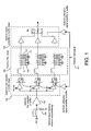
- FIG. 1 shows a tracking filter block diagram according to the present invention.
- FIG. 2 shows an LNA Calibration/AGC block diagram according to the present invention.
- FIG. 3 shows an example of a calibration procedure according to the present invention.
- FIG. 1 shows that tracking filter 100 relies on inductor and capacitor (LC) filtering using fixed inductors and variable capacitors.
- the variable capacitors are implemented as arrays of capacitors 101 with switches 102 .
- the switches can easily be implemented using metal-oxide-semiconductor (MOS) transistors but other methods are possible too such as diode switches.
- MOS metal-oxide-semiconductor
- the switches connect the capacitors to a common signal point, for example AC ground.
- the switches are shown on the AC ground side of the capacitors but could also be on the signal side of the capacitors.
- FIG. 1 shows how low noise amplifier (LNA) 104 can be split up into several banks using different values of inductors to limit the required range of each capacitor bank.
- the variable capacitors can be implemented in other well-known ways such as with varactors or a combination of varactors with switched capacitors.
- the LNA is to use active gain elements.
- Another implementation of FIG. 1 can use unity gain or low gain buffers, for example, emitter followers, and gain is provided by the tracking filter.
- the tracking filter gain is the passive voltage multiplication provided by the Q of the LC tanks; therefore, the voltage gain would be equal to Q, the circuit's quality factor.
- a circuit's Q is defined as two times the product of pi and the ratio of the maximum energy stored to the energy dissipated per cycle.
- the LNA/tracking filter can also provide voltage gain at its input due to intentionally mismatching, for example, the input impedance is set higher than the signal source impedance, which causes less voltage division from the source than if the input impedance had been power-matched.
- emitter followers in the LNA as opposed to active gain blocks enables very high linearity and high input impedance. It is especially an advantage that the load impedance for the emitter followers increases significantly for frequencies away from the resonance frequency of the LC circuit. This greatly improves linearity for jammers at larger frequency offsets from the desired channel without sacrificing noise figure for the desired signal.
- FIG. 1 shows the LNA consisting of pre-buffer or amplifier 103 driving three buffers or amplifiers, of which only one is active at a time, depending on which band is selected.
- the number of bands could be any number from 1 upwards.
- the pre-buffer can be omitted-its main benefit is to reduce parasitic loading of the RF input from the disabled tracking filter buffers.
- the switches (S 1 , S 2 , S 3 ) can be omitted if the test signal buffer is designed so that it has relatively high output impedance when off. The same argument applies to switch S 4 in stage 106 of FIG. 1 .
- the mentioned buffers do not have to be emitter-followers; they could be implemented as source followers or as any other known buffer technique.
- variable automatic gain control (AGC) gain can be obtained by using variable parallel resistors across the tank circuits, which can de-Q the filter and thereby lower the gain.
- the variability can be achieved by a resistor network 110 with switches 111 connecting the resistors to ground. This should be construed as AC ground, for example a suitable reference voltage or a capacitor connected to the circuit ground or any other technique for providing an AC signal ground. Alternatively, the switches could be placed between the resistors and the signal node. Variability of the resistors can be achieved in other well know ways, including using MOS transistors.
- the LNA optionally incorporates calibration signal input 107 . This can be used for auto-calibration of the center frequency that, for example, would determine the correct capacitor switch settings.
- the test signal can either be passed through the LNA or it can be routed directly to the output. The latter feature also enables gain calibration if desired.
- FIG. 2 shows LNA calibration circuitry comprising calibration block 200 and calibration clock generator circuit 202 .
- the purpose of the calibration circuit is twofold: to tune the filter to the desired channel by adjustment of the capacitor arrays, and to optionally adjust the gain.
- the gain can be adjusted at several locations, for example, in the LNA, before the LNA or, by adjusting the tank circuit Q and therefore the filter gain to a nominal value.
- Calibration clock generator circuit 202 produces calibration test tone 201 and clock signals for the sample/hold and state machine circuits.
- the filter calibration is done by injection of test tone 201 in the signal path and by adjustment of the capacitor array while detecting the level of the test tone after it has passed through the receiver and dedicated detection circuitry 210 .
- the filter is centered by detecting the point at which, as the capacitor array is adjusted, the receive path gain is maximized.
- One way of achieving this is to monotonically adjust the capacitor array until the gain stops increasing and starts to decrease.
- the circuit yields the peak receive path gain that is also for this filter topology the center frequency of the filter.
- This method requires some storage mechanism in order to determine change in gain from one step to the next. This can be achieved in several well-known ways, including sample-hold circuits 220 for analog implementations or registers in digital implementations.
- the gain calibration is done by injection of test tone 201 in the signal path, and establishing a reference receive path gain “A” with the LNA bypassed.
- the LNA is then switched in using the calibration through path and a new receive gain path gain “B” is established.
- the difference between “A” and “B” is the gain of the LNA and tracking filter.
- the filter gain is then optimized by adjustment of a resistor array. In one implementation, an attenuator loss of predetermined value is switched in into the calibration block during the “B” phase only.
- the filter gain is optimized by adjustment of a resistor array while detecting the level of the test tone, after passing through the receiver and dedicated detection circuitry. Path gain “B” is compared with the previously established reference receive path gain “A”.
- the filter gain is optimized and equal to the predetermined attenuator loss when gains “A” and “B” are equal, since the LNA gain exactly offsets the attenuator loss.
- the LNA gain can be precisely set and in addition, if several attenuator values are available then several LNA gain settings can be achieved. Similar to the filter calibration, a storage function is needed. For the gain calibration, the signals representing gain “B” and the previously determined gain “A” need to be stored and compared.
- FIG. 2 shows a mainly analog implementation in which the aforementioned storage function is implemented with sample-hold circuits.
- This invention also addresses some potential issues with the calibration method. Situations to consider include leakage of the test tone out the RF pins could violate emissions specifications, noise and strong co-channel interference at the input can corrupt the calibration, thus making reliable signal level measurements difficult, and off-channel jammers can corrupt calibration by overwhelming the test tone signal and thereby causing the calibration machine to center on the jammer instead of the test tone.
- test tone level control circuit can optionally be implemented which minimizes the level of the test tone while ensuring that noise or interference does not corrupt the measurement.
- the test tone level is set to a minimal value and gradually increased until a minimum required ratio of calibration test tone to noise and interference is achieved. This also ensures that emission of test tone power is minimized during the calibration period.
- FIG. 3 shows details of an example of the described calibration procedure.
- the calibration procedure can be implemented in various other ways.
- FIG. 2 shows an example implementation of an AGC loop around the LNA/tracking filter. This can take any number of inputs from any locations in the signal path.
- two sense points are used, input 203 of the mixer and input 204 of the main part of the channel filter.
- the front-end gain is determined by avoidance of overloading the channel filter as well as avoidance of overloading the mixer input. It is advantageous to use a sense point after the tracking filter but before the mixer. This enables the AGC to react to off-channel jammers.
- the jammer level at which the AGC starts reducing the gain then depends on the frequency offset from the desired channel; the further the frequency offset is, the higher the tolerable jammer level before the onset of gain reduction.
- the AGC loop can advantageously be implemented in digital form, for example as an up/down counter whose output word controls the resistor array.
- the counter would be clocked with a reference frequency and the up/down control would be determined by the outputs of the power or peak detection circuits.
- the analog outputs can be compared to reference, called “set point” values by using comparators and the digital outputs of these comparators can then be logically OR'ed together to form the up/down control signal for the counter.
- the jammers are analog video signals asymmetric AGC attack and decay times can be used, one implementation would be to sample a number of consecutive samples of the error signal to detect a ramp up/down and use this to slow down the counter clock using a divider.
- a maximum filter Q can be set by limiting the maximum value of the variable resistors.
- One way to implement a resistance limit with switched resistors is to have a separate control register to store the limit value; the value may be different based on frequency. The resistor control word is then prevented from setting the resistance beyond the limit value.
Abstract
Description
Claims (10)
Priority Applications (1)
| Application Number | Priority Date | Filing Date | Title |
|---|---|---|---|
| US11/302,876 US8340616B2 (en) | 2004-12-16 | 2005-12-14 | Tracking filter for tuner |
Applications Claiming Priority (2)
| Application Number | Priority Date | Filing Date | Title |
|---|---|---|---|
| US63655604P | 2004-12-16 | 2004-12-16 | |
| US11/302,876 US8340616B2 (en) | 2004-12-16 | 2005-12-14 | Tracking filter for tuner |
Publications (2)
| Publication Number | Publication Date |
|---|---|
| US20060154636A1 US20060154636A1 (en) | 2006-07-13 |
| US8340616B2 true US8340616B2 (en) | 2012-12-25 |
Family
ID=36653911
Family Applications (1)
| Application Number | Title | Priority Date | Filing Date |
|---|---|---|---|
| US11/302,876 Expired - Fee Related US8340616B2 (en) | 2004-12-16 | 2005-12-14 | Tracking filter for tuner |
Country Status (1)
| Country | Link |
|---|---|
| US (1) | US8340616B2 (en) |
Cited By (4)
| Publication number | Priority date | Publication date | Assignee | Title |
|---|---|---|---|---|
| US20130040595A1 (en) * | 2010-04-21 | 2013-02-14 | Beijing Kt Micro, Ltd. | Circuit For A Front-End Tunable Filter of A Communication and Broadcast Receiver and A tuning Method thereof |
| US20140253249A1 (en) * | 2013-03-11 | 2014-09-11 | Mediatek Singapore Pte. Ltd. | Circuit for providing a flat gain response over a selected frequency range and method of use |
| US20190393841A1 (en) * | 2017-06-16 | 2019-12-26 | Nippon Telegraph And Telephone Corporation | Amplifier |
| US11438002B2 (en) * | 2020-03-06 | 2022-09-06 | Omni Design Technologies Inc. | Time-interleaved A/D converters with isolation inductors |
Families Citing this family (19)
| Publication number | Priority date | Publication date | Assignee | Title |
|---|---|---|---|---|
| US7336939B2 (en) * | 2003-05-21 | 2008-02-26 | Broadcom Corporation | Integrated tracking filters for direct conversion and low-IF single conversion broadband filters |
| KR100692306B1 (en) * | 2005-04-01 | 2007-03-09 | 인티그런트 테크놀로지즈(주) | Tracking filter for tuning channel in wide-band |
| US7474160B2 (en) * | 2005-05-25 | 2009-01-06 | Qualcomm Incorporated | Systems and methods for calibrating a filter |
| GB2427088B (en) * | 2005-06-08 | 2008-12-24 | Zarlink Semiconductor Ltd | Radio frequency tuner |
| US20070206705A1 (en) * | 2006-03-03 | 2007-09-06 | Applied Wireless Identification Group, Inc. | RFID reader with adjustable filtering and adaptive backscatter processing |
| US20070105514A1 (en) * | 2005-11-08 | 2007-05-10 | Chao-Wen Tseng | Low Noise, High Linearity TV Tuner Architecture with Switched Fixed-Gain LNA |
| US8150351B2 (en) * | 2006-04-17 | 2012-04-03 | Entropic Communications, Inc. | Receiver with tuner front end using tracking filters and calibration |
| US20080111623A1 (en) * | 2006-11-15 | 2008-05-15 | Microtune (Texas), L.P. | Input signal power control |
| US7715813B2 (en) * | 2007-01-15 | 2010-05-11 | Mediatek Singapore Pte Ltd | Receiver having tunable amplifier with integrated tracking filter |
| US8090332B2 (en) * | 2007-12-12 | 2012-01-03 | Qualcomm, Incorporated | Tracking filter for a receiver |
| US8374566B2 (en) * | 2008-04-04 | 2013-02-12 | Nxp B.V. | Integrated wideband RF tracking filter for RF front end with parallel band switched tuned amplifiers |
| US8331897B2 (en) * | 2008-04-07 | 2012-12-11 | Qualcomm Incorporated | Highly linear embedded filtering passive mixer |
| US8385867B2 (en) * | 2009-06-29 | 2013-02-26 | Silicon Laboratories Inc. | Tracking filter for a television tuner |
| GB2472273A (en) * | 2009-07-31 | 2011-02-02 | Cambridge Silicon Radio Ltd | Fine gain adjustment of tuned circuit for UWB receiver |
| US8428533B2 (en) * | 2010-06-08 | 2013-04-23 | Qualcomm, Incorporated | Techniques for optimizing gain or noise figure of an RF receiver |
| JP2012034191A (en) * | 2010-07-30 | 2012-02-16 | Panasonic Corp | Semiconductor integrated circuit and tuner system having the same |
| US8649302B2 (en) * | 2011-02-15 | 2014-02-11 | Intel Mobile Communications GmbH | Receiver for receiving RF-signals in a plurality of different communication bands and transceiver |
| US9793935B2 (en) * | 2015-07-02 | 2017-10-17 | Mediatek Inc. | Multi-mixer system and method for reducing interference within multi-mixer system |
| US10340860B1 (en) * | 2018-09-21 | 2019-07-02 | Qualcomm Incorporated | Multi-mode low noise amplifier |
Citations (17)
| Publication number | Priority date | Publication date | Assignee | Title |
|---|---|---|---|---|
| US4685150A (en) | 1983-03-11 | 1987-08-04 | Deutsche Thomson-Brandt Gmbh | Tuning of a resonant circuit in a communications receiver |
| DE4329705A1 (en) | 1993-09-02 | 1995-03-09 | Froehlich Reimar Dr Ing | Circuit arrangement for microcomputer-controllable inductors, capacitors and L/C circuits |
| DE19904604A1 (en) | 1999-02-05 | 2000-06-15 | Temic Semiconductor Gmbh | Circuit layout and method for adjusting a band filter in a radio receiver has a band filter, a voltage-controlled oscillator, a tuner, a reference oscillator, a phase locked loop (PLL) actuator, an equalizer and a micro-controller. |
| US6175274B1 (en) * | 1999-07-26 | 2001-01-16 | Nokia Mobile Phones Limited | Switched gain low noise amplifier |
| US6307442B1 (en) * | 1999-05-17 | 2001-10-23 | Maxim Integrated Products | Enhanced LC filter with tunable Q |
| US6525609B1 (en) * | 1998-11-12 | 2003-02-25 | Broadcom Corporation | Large gain range, high linearity, low noise MOS VGA |
| US6686809B2 (en) * | 2001-03-09 | 2004-02-03 | National Semiconductor Corporation | Filter trimming |
| US6731175B1 (en) * | 2002-06-20 | 2004-05-04 | Faraday Technology Corp. | High frequency amplifier |
| US6750734B2 (en) * | 2002-05-29 | 2004-06-15 | Ukom, Inc. | Methods and apparatus for tuning an LC filter |
| US6778023B2 (en) * | 2001-07-31 | 2004-08-17 | Nokia Corporation | Tunable filter and method of tuning a filter |
| US6823292B2 (en) * | 2001-11-01 | 2004-11-23 | Koninklijke Philips Electronics N.V. | Tuneable filter |
| US20050012565A1 (en) * | 2003-07-18 | 2005-01-20 | Takatsugu Kamata | Methods and apparatus for an improved discrete LC filter |
| US6954115B2 (en) * | 2002-05-29 | 2005-10-11 | Rf Stream Corporation | Methods and apparatus for tuning successive approximation |
| US6965275B2 (en) * | 2004-02-13 | 2005-11-15 | Infineon Technologies Ag | Method and apparatus for tuning a filter |
| US7076225B2 (en) * | 2001-02-16 | 2006-07-11 | Qualcomm Incorporated | Variable gain selection in direct conversion receiver |
| US7323945B2 (en) * | 2004-02-10 | 2008-01-29 | Bitwave Semiconductor, Inc. | Programmable radio transceiver |
| US7346324B2 (en) * | 2003-09-29 | 2008-03-18 | Sharp Kabushiki Kaisha | Grounded-emitter circuit, and high-frequency receiver and high-frequency transmitter using the same |
-
2005
- 2005-12-14 US US11/302,876 patent/US8340616B2/en not_active Expired - Fee Related
Patent Citations (20)
| Publication number | Priority date | Publication date | Assignee | Title |
|---|---|---|---|---|
| US4685150A (en) | 1983-03-11 | 1987-08-04 | Deutsche Thomson-Brandt Gmbh | Tuning of a resonant circuit in a communications receiver |
| DE4329705A1 (en) | 1993-09-02 | 1995-03-09 | Froehlich Reimar Dr Ing | Circuit arrangement for microcomputer-controllable inductors, capacitors and L/C circuits |
| US6525609B1 (en) * | 1998-11-12 | 2003-02-25 | Broadcom Corporation | Large gain range, high linearity, low noise MOS VGA |
| DE19904604A1 (en) | 1999-02-05 | 2000-06-15 | Temic Semiconductor Gmbh | Circuit layout and method for adjusting a band filter in a radio receiver has a band filter, a voltage-controlled oscillator, a tuner, a reference oscillator, a phase locked loop (PLL) actuator, an equalizer and a micro-controller. |
| US6307442B1 (en) * | 1999-05-17 | 2001-10-23 | Maxim Integrated Products | Enhanced LC filter with tunable Q |
| US6175274B1 (en) * | 1999-07-26 | 2001-01-16 | Nokia Mobile Phones Limited | Switched gain low noise amplifier |
| US7076225B2 (en) * | 2001-02-16 | 2006-07-11 | Qualcomm Incorporated | Variable gain selection in direct conversion receiver |
| US20040212447A1 (en) | 2001-03-09 | 2004-10-28 | Christian Nystrom | Filter trimming |
| US7002427B2 (en) * | 2001-03-09 | 2006-02-21 | National Semiconductor Corporation | Filter trimming |
| US6686809B2 (en) * | 2001-03-09 | 2004-02-03 | National Semiconductor Corporation | Filter trimming |
| US6778023B2 (en) * | 2001-07-31 | 2004-08-17 | Nokia Corporation | Tunable filter and method of tuning a filter |
| US6823292B2 (en) * | 2001-11-01 | 2004-11-23 | Koninklijke Philips Electronics N.V. | Tuneable filter |
| US6750734B2 (en) * | 2002-05-29 | 2004-06-15 | Ukom, Inc. | Methods and apparatus for tuning an LC filter |
| US6954115B2 (en) * | 2002-05-29 | 2005-10-11 | Rf Stream Corporation | Methods and apparatus for tuning successive approximation |
| US6731175B1 (en) * | 2002-06-20 | 2004-05-04 | Faraday Technology Corp. | High frequency amplifier |
| US20050012565A1 (en) * | 2003-07-18 | 2005-01-20 | Takatsugu Kamata | Methods and apparatus for an improved discrete LC filter |
| US7183880B2 (en) * | 2003-07-18 | 2007-02-27 | Rfstream Corporation | Discrete inductor bank and LC filter |
| US7346324B2 (en) * | 2003-09-29 | 2008-03-18 | Sharp Kabushiki Kaisha | Grounded-emitter circuit, and high-frequency receiver and high-frequency transmitter using the same |
| US7323945B2 (en) * | 2004-02-10 | 2008-01-29 | Bitwave Semiconductor, Inc. | Programmable radio transceiver |
| US6965275B2 (en) * | 2004-02-13 | 2005-11-15 | Infineon Technologies Ag | Method and apparatus for tuning a filter |
Non-Patent Citations (1)
| Title |
|---|
| Frederik Emmons Terman, "Radio Engineering", 1947, p. 39-p. 52, McGraw-Hill Book Company, Inc, New York and London. |
Cited By (11)
| Publication number | Priority date | Publication date | Assignee | Title |
|---|---|---|---|---|
| US20130040595A1 (en) * | 2010-04-21 | 2013-02-14 | Beijing Kt Micro, Ltd. | Circuit For A Front-End Tunable Filter of A Communication and Broadcast Receiver and A tuning Method thereof |
| US8862089B2 (en) * | 2010-04-21 | 2014-10-14 | Beijing Kt Micro, Ltd. | Circuit for a front-end tunable filter of a communication and broadcast receiver and a tuning method thereof |
| US20140253249A1 (en) * | 2013-03-11 | 2014-09-11 | Mediatek Singapore Pte. Ltd. | Circuit for providing a flat gain response over a selected frequency range and method of use |
| CN104052408A (en) * | 2013-03-11 | 2014-09-17 | 联发科技(新加坡)私人有限公司 | Integrated circuit |
| US9166545B2 (en) * | 2013-03-11 | 2015-10-20 | Mediatek Singapore Ptd. Ltd. | Circuit for providing a flat gain response over a selected frequency range and method of use |
| CN104052408B (en) * | 2013-03-11 | 2017-04-12 | 联发科技(新加坡)私人有限公司 | Integrated circuit |
| US20190393841A1 (en) * | 2017-06-16 | 2019-12-26 | Nippon Telegraph And Telephone Corporation | Amplifier |
| US10804857B2 (en) * | 2017-06-16 | 2020-10-13 | Nippon Telegraph And Telephone Corporation | Amplifier |
| US11438002B2 (en) * | 2020-03-06 | 2022-09-06 | Omni Design Technologies Inc. | Time-interleaved A/D converters with isolation inductors |
| US20220337267A1 (en) * | 2020-03-06 | 2022-10-20 | Omni Design Technologies Inc. | Time-interleaved a/d converters with isolation inductors |
| US11770128B2 (en) * | 2020-03-06 | 2023-09-26 | Omni Design Technologies Inc. | Time-interleaved A/D converters with isolation inductors |
Also Published As
| Publication number | Publication date |
|---|---|
| US20060154636A1 (en) | 2006-07-13 |
Similar Documents
| Publication | Publication Date | Title |
|---|---|---|
| US8340616B2 (en) | Tracking filter for tuner | |
| US7620379B2 (en) | Radio frequency tuner | |
| US4247953A (en) | Tunable high-frequency input circuit | |
| US7095454B2 (en) | Broadband single conversion tuner integrated circuits | |
| US8150351B2 (en) | Receiver with tuner front end using tracking filters and calibration | |
| US20050040909A1 (en) | Broadband integrated digitally tunable filters | |
| US7983644B2 (en) | Apparatus and method for local oscillator calibration in mixer circuits | |
| US20100149431A1 (en) | Active Inductor Circuits for Filtering in a Cable Tuner Circuit | |
| EP1911167B1 (en) | Boosted-bias tunable filter with run-time calibration | |
| US7006162B2 (en) | Tuner | |
| US4771332A (en) | Tuning apparatus for the VHF band of a television receiver | |
| US20050118968A1 (en) | Double conversion tuner | |
| US6950152B2 (en) | Television tuner which has leveled a gain deviation in the same band | |
| US7283795B2 (en) | Receiver device having improved selectivity characteristics | |
| US7054606B1 (en) | Digitally calibrated narrowband filter with analog channel compensation | |
| US20030220088A1 (en) | Tuner | |
| US7155189B2 (en) | AM receiver | |
| US6864924B2 (en) | Television tuner input circuit having satisfactory selection properties at high band reception | |
| US20010027093A1 (en) | Circuit configuration for filtering a radio-frequency signal | |
| WO2006066000A1 (en) | Tracking filter for tuner | |
| JPH0730456A (en) | Television tuner | |
| US7158772B1 (en) | Filter for broadcast receiver tuner | |
| GB2362049A (en) | Double-tuned band switching circuit for high, low and middle band VHF with inductive coupling | |
| JP2004357174A (en) | Input circuit for electronic tuner | |
| JPH06140957A (en) | U-v tuner |
Legal Events
| Date | Code | Title | Description |
|---|---|---|---|
| AS | Assignment |
Owner name: RF MAGIC, INC., CALIFORNIA Free format text: ASSIGNMENT OF ASSIGNORS INTEREST;ASSIGNOR:SHAH, PETER JIVAN;REEL/FRAME:017665/0504 Effective date: 20060308 |
|
| STCF | Information on status: patent grant |
Free format text: PATENTED CASE |
|
| AS | Assignment |
Owner name: ENTROPIC COMMUNICATIONS, INC., CALIFORNIA Free format text: MERGER AND CHANGE OF NAME;ASSIGNORS:EXCALIBUR ACQUISITION CORPORATION;ENTROPIC COMMUNICATIONS, INC.;ENTROPIC COMMUNICATIONS, INC.;REEL/FRAME:035706/0267 Effective date: 20150430 |
|
| AS | Assignment |
Owner name: ENTROPIC COMMUNICATIONS, LLC, CALIFORNIA Free format text: MERGER AND CHANGE OF NAME;ASSIGNORS:ENTROPIC COMMUNICATIONS, INC.;EXCALIBUR SUBSIDIARY, LLC;ENTROPIC COMMUNICATIONS, LLC;REEL/FRAME:035717/0628 Effective date: 20150430 |
|
| FPAY | Fee payment |
Year of fee payment: 4 |
|
| AS | Assignment |
Owner name: ENTROPIC COMMUNICATIONS INC., CALIFORNIA Free format text: ASSIGNMENT OF ASSIGNORS INTEREST;ASSIGNOR:RF MAGIC, INC.;REEL/FRAME:042211/0977 Effective date: 20140401 |
|
| AS | Assignment |
Owner name: JPMORGAN CHASE BANK, N.A., AS COLLATERAL AGENT, IL Free format text: SECURITY AGREEMENT;ASSIGNORS:MAXLINEAR, INC.;ENTROPIC COMMUNICATIONS, LLC (F/K/A ENTROPIC COMMUNICATIONS, INC.);EXAR CORPORATION;REEL/FRAME:042453/0001 Effective date: 20170512 Owner name: JPMORGAN CHASE BANK, N.A., AS COLLATERAL AGENT, ILLINOIS Free format text: SECURITY AGREEMENT;ASSIGNORS:MAXLINEAR, INC.;ENTROPIC COMMUNICATIONS, LLC (F/K/A ENTROPIC COMMUNICATIONS, INC.);EXAR CORPORATION;REEL/FRAME:042453/0001 Effective date: 20170512 |
|
| AS | Assignment |
Owner name: MUFG UNION BANK, N.A., CALIFORNIA Free format text: SUCCESSION OF AGENCY (REEL 042453 / FRAME 0001);ASSIGNOR:JPMORGAN CHASE BANK, N.A.;REEL/FRAME:053115/0842 Effective date: 20200701 |
|
| FEPP | Fee payment procedure |
Free format text: MAINTENANCE FEE REMINDER MAILED (ORIGINAL EVENT CODE: REM.); ENTITY STATUS OF PATENT OWNER: LARGE ENTITY |
|
| LAPS | Lapse for failure to pay maintenance fees |
Free format text: PATENT EXPIRED FOR FAILURE TO PAY MAINTENANCE FEES (ORIGINAL EVENT CODE: EXP.); ENTITY STATUS OF PATENT OWNER: LARGE ENTITY |
|
| STCH | Information on status: patent discontinuation |
Free format text: PATENT EXPIRED DUE TO NONPAYMENT OF MAINTENANCE FEES UNDER 37 CFR 1.362 |
|
| FP | Lapsed due to failure to pay maintenance fee |
Effective date: 20201225 |
|
| AS | Assignment |
Owner name: MAXLINEAR, INC., CALIFORNIA Free format text: RELEASE BY SECURED PARTY;ASSIGNOR:MUFG UNION BANK, N.A.;REEL/FRAME:056656/0204 Effective date: 20210623 Owner name: EXAR CORPORATION, CALIFORNIA Free format text: RELEASE BY SECURED PARTY;ASSIGNOR:MUFG UNION BANK, N.A.;REEL/FRAME:056656/0204 Effective date: 20210623 Owner name: MAXLINEAR COMMUNICATIONS LLC, CALIFORNIA Free format text: RELEASE BY SECURED PARTY;ASSIGNOR:MUFG UNION BANK, N.A.;REEL/FRAME:056656/0204 Effective date: 20210623 |