US8337959B2 - Method and apparatus to apply surface release coating for imprint mold - Google Patents
Method and apparatus to apply surface release coating for imprint mold Download PDFInfo
- Publication number
- US8337959B2 US8337959B2 US11/945,470 US94547007A US8337959B2 US 8337959 B2 US8337959 B2 US 8337959B2 US 94547007 A US94547007 A US 94547007A US 8337959 B2 US8337959 B2 US 8337959B2
- Authority
- US
- United States
- Prior art keywords
- chamber
- workpiece
- mold
- vapor
- deposition
- Prior art date
- Legal status (The legal status is an assumption and is not a legal conclusion. Google has not performed a legal analysis and makes no representation as to the accuracy of the status listed.)
- Active, expires
Links
- 238000000034 method Methods 0.000 title claims abstract description 42
- 238000000576 coating method Methods 0.000 title description 19
- 239000011248 coating agent Substances 0.000 title description 18
- 239000004094 surface-active agent Substances 0.000 claims abstract description 60
- 239000000758 substrate Substances 0.000 claims abstract description 28
- 238000004140 cleaning Methods 0.000 claims abstract description 22
- 238000001459 lithography Methods 0.000 claims abstract description 20
- 230000008021 deposition Effects 0.000 claims abstract description 16
- 238000001947 vapour-phase growth Methods 0.000 claims abstract description 11
- CBENFWSGALASAD-UHFFFAOYSA-N Ozone Chemical compound [O-][O+]=O CBENFWSGALASAD-UHFFFAOYSA-N 0.000 claims abstract description 8
- 238000011109 contamination Methods 0.000 claims abstract description 6
- 239000002318 adhesion promoter Substances 0.000 claims abstract description 5
- 238000000151 deposition Methods 0.000 claims description 18
- XLYOFNOQVPJJNP-UHFFFAOYSA-N water Chemical compound O XLYOFNOQVPJJNP-UHFFFAOYSA-N 0.000 claims description 15
- 238000006243 chemical reaction Methods 0.000 claims description 9
- 239000000463 material Substances 0.000 claims description 8
- 239000007791 liquid phase Substances 0.000 claims description 7
- 238000010521 absorption reaction Methods 0.000 claims description 4
- 239000012530 fluid Substances 0.000 claims description 4
- QRPMCZNLJXJVSG-UHFFFAOYSA-N trichloro(1,1,2,2,3,3,4,4,5,5,6,6,7,7,8,8,9,9,10,10,10-henicosafluorodecyl)silane Chemical compound FC(F)(F)C(F)(F)C(F)(F)C(F)(F)C(F)(F)C(F)(F)C(F)(F)C(F)(F)C(F)(F)C(F)(F)[Si](Cl)(Cl)Cl QRPMCZNLJXJVSG-UHFFFAOYSA-N 0.000 claims description 4
- LEPRPXBFZRAOGU-UHFFFAOYSA-N 3-trichlorosilylpropyl prop-2-enoate Chemical compound Cl[Si](Cl)(Cl)CCCOC(=O)C=C LEPRPXBFZRAOGU-UHFFFAOYSA-N 0.000 claims description 3
- 238000010926 purge Methods 0.000 claims description 3
- HVRIKLVHKQKDAZ-UHFFFAOYSA-N FC(C(C(F)(F)F)(F)F)([Si](Cl)(Cl)Cl)C(C(C(C(C(C(F)(F)F)(F)F)(F)F)(F)F)(F)F)(F)F Chemical compound FC(C(C(F)(F)F)(F)F)([Si](Cl)(Cl)Cl)C(C(C(C(C(C(F)(F)F)(F)F)(F)F)(F)F)(F)F)(F)F HVRIKLVHKQKDAZ-UHFFFAOYSA-N 0.000 claims description 2
- SBSCMBQZVCGKFP-UHFFFAOYSA-N bromo-dichloro-(1,1,2,2,3,3,4,4,5,5,6,6,7,7,8,8,9,9,10,10,10-henicosafluorodecyl)germane Chemical compound FC(F)(F)C(F)(F)C(F)(F)C(F)(F)C(F)(F)C(F)(F)C(F)(F)C(F)(F)C(F)(F)C(F)(F)[Ge](Cl)(Cl)Br SBSCMBQZVCGKFP-UHFFFAOYSA-N 0.000 claims description 2
- OMBLNHKTSXMFDO-UHFFFAOYSA-N bromo-dichloro-(1,1,2,2,3,3,4,4,5,5,6,6,7,7,8,8,9,9,10,10,10-henicosafluorodecyl)silane Chemical compound FC(F)(F)C(F)(F)C(F)(F)C(F)(F)C(F)(F)C(F)(F)C(F)(F)C(F)(F)C(F)(F)C(F)(F)[Si](Cl)(Cl)Br OMBLNHKTSXMFDO-UHFFFAOYSA-N 0.000 claims description 2
- OTBGVKCQFOAAQH-UHFFFAOYSA-N trichloro(1,1,2,2,3,3,4,4,5,5,6,6,6-tridecafluorohexyl)silane Chemical compound FC(F)(F)C(F)(F)C(F)(F)C(F)(F)C(F)(F)C(F)(F)[Si](Cl)(Cl)Cl OTBGVKCQFOAAQH-UHFFFAOYSA-N 0.000 claims description 2
- AVXLXFZNRNUCRP-UHFFFAOYSA-N trichloro(1,1,2,2,3,3,4,4,5,5,6,6,7,7,8,8,8-heptadecafluorooctyl)silane Chemical compound FC(F)(F)C(F)(F)C(F)(F)C(F)(F)C(F)(F)C(F)(F)C(F)(F)C(F)(F)[Si](Cl)(Cl)Cl AVXLXFZNRNUCRP-UHFFFAOYSA-N 0.000 claims description 2
- 239000005052 trichlorosilane Substances 0.000 claims description 2
- 230000003213 activating effect Effects 0.000 claims 1
- 238000012544 monitoring process Methods 0.000 claims 1
- 239000012071 phase Substances 0.000 claims 1
- 239000007788 liquid Substances 0.000 abstract description 24
- 230000008016 vaporization Effects 0.000 abstract description 9
- 238000009834 vaporization Methods 0.000 abstract description 8
- 238000010438 heat treatment Methods 0.000 abstract description 5
- 150000002500 ions Chemical class 0.000 abstract description 4
- 238000002347 injection Methods 0.000 abstract description 3
- 239000007924 injection Substances 0.000 abstract description 3
- 238000000926 separation method Methods 0.000 abstract description 3
- 239000007921 spray Substances 0.000 abstract description 2
- 239000007789 gas Substances 0.000 description 23
- 239000000126 substance Substances 0.000 description 15
- IJGRMHOSHXDMSA-UHFFFAOYSA-N Atomic nitrogen Chemical compound N#N IJGRMHOSHXDMSA-UHFFFAOYSA-N 0.000 description 12
- 239000011800 void material Substances 0.000 description 9
- 238000007654 immersion Methods 0.000 description 7
- XKRFYHLGVUSROY-UHFFFAOYSA-N Argon Chemical compound [Ar] XKRFYHLGVUSROY-UHFFFAOYSA-N 0.000 description 6
- 229910052757 nitrogen Inorganic materials 0.000 description 6
- 238000005086 pumping Methods 0.000 description 6
- 238000007740 vapor deposition Methods 0.000 description 6
- 239000010408 film Substances 0.000 description 4
- 239000004809 Teflon Substances 0.000 description 3
- 229920006362 Teflon® Polymers 0.000 description 3
- 239000003570 air Substances 0.000 description 3
- 229910052786 argon Inorganic materials 0.000 description 3
- 239000001307 helium Substances 0.000 description 3
- 229910052734 helium Inorganic materials 0.000 description 3
- SWQJXJOGLNCZEY-UHFFFAOYSA-N helium atom Chemical compound [He] SWQJXJOGLNCZEY-UHFFFAOYSA-N 0.000 description 3
- 230000005855 radiation Effects 0.000 description 3
- 239000010409 thin film Substances 0.000 description 3
- 230000008901 benefit Effects 0.000 description 2
- 239000011261 inert gas Substances 0.000 description 2
- 238000004519 manufacturing process Methods 0.000 description 2
- 238000000465 moulding Methods 0.000 description 2
- 238000001127 nanoimprint lithography Methods 0.000 description 2
- 238000000206 photolithography Methods 0.000 description 2
- 229920000642 polymer Polymers 0.000 description 2
- 239000010453 quartz Substances 0.000 description 2
- 238000007789 sealing Methods 0.000 description 2
- 239000004065 semiconductor Substances 0.000 description 2
- VYPSYNLAJGMNEJ-UHFFFAOYSA-N silicon dioxide Inorganic materials O=[Si]=O VYPSYNLAJGMNEJ-UHFFFAOYSA-N 0.000 description 2
- 229910001220 stainless steel Inorganic materials 0.000 description 2
- 239000010935 stainless steel Substances 0.000 description 2
- WMJWAOGCUJJPRD-UHFFFAOYSA-K FC(F)(F)C(F)(F)C(F)(F)C(F)(F)C(F)(F)C(F)(F)C(F)(F)C(F)(F)C(F)(F)C(F)(F)[Ti](Cl)(Cl)Cl Chemical compound FC(F)(F)C(F)(F)C(F)(F)C(F)(F)C(F)(F)C(F)(F)C(F)(F)C(F)(F)C(F)(F)C(F)(F)[Ti](Cl)(Cl)Cl WMJWAOGCUJJPRD-UHFFFAOYSA-K 0.000 description 1
- 238000003848 UV Light-Curing Methods 0.000 description 1
- XAGFODPZIPBFFR-UHFFFAOYSA-N aluminium Chemical compound [Al] XAGFODPZIPBFFR-UHFFFAOYSA-N 0.000 description 1
- 229910052782 aluminium Inorganic materials 0.000 description 1
- QVGXLLKOCUKJST-UHFFFAOYSA-N atomic oxygen Chemical compound [O] QVGXLLKOCUKJST-UHFFFAOYSA-N 0.000 description 1
- 238000007664 blowing Methods 0.000 description 1
- 238000005229 chemical vapour deposition Methods 0.000 description 1
- 239000002894 chemical waste Substances 0.000 description 1
- 238000012864 cross contamination Methods 0.000 description 1
- 238000005137 deposition process Methods 0.000 description 1
- 238000001312 dry etching Methods 0.000 description 1
- 238000001704 evaporation Methods 0.000 description 1
- 230000008020 evaporation Effects 0.000 description 1
- 239000011521 glass Substances 0.000 description 1
- 231100001261 hazardous Toxicity 0.000 description 1
- 238000007373 indentation Methods 0.000 description 1
- 230000010354 integration Effects 0.000 description 1
- 238000002955 isolation Methods 0.000 description 1
- 238000002156 mixing Methods 0.000 description 1
- 239000000203 mixture Substances 0.000 description 1
- 230000003287 optical effect Effects 0.000 description 1
- 239000001301 oxygen Substances 0.000 description 1
- 229910052760 oxygen Inorganic materials 0.000 description 1
- 238000004886 process control Methods 0.000 description 1
- 229910052710 silicon Inorganic materials 0.000 description 1
- 239000010703 silicon Substances 0.000 description 1
- 239000007787 solid Substances 0.000 description 1
- 238000004544 sputter deposition Methods 0.000 description 1
- 238000003860 storage Methods 0.000 description 1
- 238000001029 thermal curing Methods 0.000 description 1
- VIFIHLXNOOCGLJ-UHFFFAOYSA-N trichloro(3,3,4,4,5,5,6,6,7,7,8,8,9,9,10,10,10-heptadecafluorodecyl)silane Chemical compound FC(F)(F)C(F)(F)C(F)(F)C(F)(F)C(F)(F)C(F)(F)C(F)(F)C(F)(F)CC[Si](Cl)(Cl)Cl VIFIHLXNOOCGLJ-UHFFFAOYSA-N 0.000 description 1
- 238000013022 venting Methods 0.000 description 1
- 238000001039 wet etching Methods 0.000 description 1
Images


Classifications
-
- H—ELECTRICITY
- H01—ELECTRIC ELEMENTS
- H01J—ELECTRIC DISCHARGE TUBES OR DISCHARGE LAMPS
- H01J37/00—Discharge tubes with provision for introducing objects or material to be exposed to the discharge, e.g. for the purpose of examination or processing thereof
- H01J37/32—Gas-filled discharge tubes
- H01J37/32431—Constructional details of the reactor
-
- B—PERFORMING OPERATIONS; TRANSPORTING
- B82—NANOTECHNOLOGY
- B82Y—SPECIFIC USES OR APPLICATIONS OF NANOSTRUCTURES; MEASUREMENT OR ANALYSIS OF NANOSTRUCTURES; MANUFACTURE OR TREATMENT OF NANOSTRUCTURES
- B82Y10/00—Nanotechnology for information processing, storage or transmission, e.g. quantum computing or single electron logic
-
- B—PERFORMING OPERATIONS; TRANSPORTING
- B82—NANOTECHNOLOGY
- B82Y—SPECIFIC USES OR APPLICATIONS OF NANOSTRUCTURES; MEASUREMENT OR ANALYSIS OF NANOSTRUCTURES; MANUFACTURE OR TREATMENT OF NANOSTRUCTURES
- B82Y40/00—Manufacture or treatment of nanostructures
-
- C—CHEMISTRY; METALLURGY
- C23—COATING METALLIC MATERIAL; COATING MATERIAL WITH METALLIC MATERIAL; CHEMICAL SURFACE TREATMENT; DIFFUSION TREATMENT OF METALLIC MATERIAL; COATING BY VACUUM EVAPORATION, BY SPUTTERING, BY ION IMPLANTATION OR BY CHEMICAL VAPOUR DEPOSITION, IN GENERAL; INHIBITING CORROSION OF METALLIC MATERIAL OR INCRUSTATION IN GENERAL
- C23C—COATING METALLIC MATERIAL; COATING MATERIAL WITH METALLIC MATERIAL; SURFACE TREATMENT OF METALLIC MATERIAL BY DIFFUSION INTO THE SURFACE, BY CHEMICAL CONVERSION OR SUBSTITUTION; COATING BY VACUUM EVAPORATION, BY SPUTTERING, BY ION IMPLANTATION OR BY CHEMICAL VAPOUR DEPOSITION, IN GENERAL
- C23C14/00—Coating by vacuum evaporation, by sputtering or by ion implantation of the coating forming material
- C23C14/06—Coating by vacuum evaporation, by sputtering or by ion implantation of the coating forming material characterised by the coating material
- C23C14/12—Organic material
-
- G—PHYSICS
- G03—PHOTOGRAPHY; CINEMATOGRAPHY; ANALOGOUS TECHNIQUES USING WAVES OTHER THAN OPTICAL WAVES; ELECTROGRAPHY; HOLOGRAPHY
- G03F—PHOTOMECHANICAL PRODUCTION OF TEXTURED OR PATTERNED SURFACES, e.g. FOR PRINTING, FOR PROCESSING OF SEMICONDUCTOR DEVICES; MATERIALS THEREFOR; ORIGINALS THEREFOR; APPARATUS SPECIALLY ADAPTED THEREFOR
- G03F7/00—Photomechanical, e.g. photolithographic, production of textured or patterned surfaces, e.g. printing surfaces; Materials therefor, e.g. comprising photoresists; Apparatus specially adapted therefor
- G03F7/0002—Lithographic processes using patterning methods other than those involving the exposure to radiation, e.g. by stamping
-
- H—ELECTRICITY
- H01—ELECTRIC ELEMENTS
- H01J—ELECTRIC DISCHARGE TUBES OR DISCHARGE LAMPS
- H01J2237/00—Discharge tubes exposing object to beam, e.g. for analysis treatment, etching, imaging
- H01J2237/32—Processing objects by plasma generation
- H01J2237/33—Processing objects by plasma generation characterised by the type of processing
- H01J2237/335—Cleaning
- H01J2237/3355—Holes or apertures, i.e. inprinted circuit boards
Definitions
- This invention relates to treating molds and substrates for imprint lithography, and in particular, to an integrated cleaning/deposition process and related apparatus.
- Lithography is a key process in the fabrication of semiconductor integrated circuits and many optical, magnetic, biological, and electro-mechanical devices. Lithography creates a pattern on a substrate-supported moldable film so that, in subsequent process steps, the pattern can be replicated in the substrate or in another material that is added onto the substrate.
- photolithography Conventional lithography, referred to as photolithography, involves applying a thin film of photosensitive resist to a substrate, exposing the resist to a desired pattern of radiation and developing the exposed resist to produce a physical pattern on the substrate.
- the resolution of patterns produced by photolithography is limited by the wavelength of the exposing radiation.
- pattern features become smaller, increasingly expensive shorter wavelength equipment is required.
- Imprint lithography based on a fundamentally different principle, offers high resolution, high throughput, low cost and the potential of large area coverage.
- imprint lithography a mold with a pattern of projecting and recessed features is pressed into a moldable surface, typically a thin film, deforming the shape of the film and forming a relief pattern in the film.
- the film is hardened, as by UV or thermal curing, and the mold and imprinted substrate are separated. After the mold is removed, the thin film can be processed, as by removing the residual reduced thickness portions to expose the underlying substrate for further processing.
- Imprint lithography can be used to replicate patterns having high resolution features in the microscale and nanoscale ranges.
- nanoscale imprint lithography Details of nanoscale imprint lithography (“nanoimprint lithography”) are described in U.S. Pat. No. 5,772,905 issued Jun. 30, 1998 and entitled “Nanoimprint Lithography”. The '905 patent is incorporated herein by reference.
- a significant factor for commercial imprint lithography is the useful life of the imprint mold.
- the mold lifetime directly affects cost of the products and throughput of the production.
- the lifetime of the imprint mold is limited by wearing of the mold surface release coating and damage to the mold material.
- the material damage, such as breaks, surface feature rupture, and surface indentation is caused by the stress and strain of imprinting.
- Wearing of the surface release coating depends on the surface chemistry, bonding strength and the coverage of the surface release layer. It is also affected by how well the release layer is applied on the mold surface. Reliable methods of applying a surface release layer are much needed for imprint lithography.
- the mold is coated with a surface release layer for a non-sticking separation. Bonding strength of the release layer to the mold depends on the cleanness of the surface and the process of release layer deposition.
- the mold is disposed in an evacuable chamber, cleaned to remove surface organic contamination and coated with the surface release layer in a chamber, all without relocation or undesired time delay.
- the chamber encloses a support chuck for the mold or substrate, a surface cleaner unit adjacent the support, a heating source adjacent the support, and advantageously, sensors for measuring chamber pressure, vapor partial pressure and moisture concentration.
- a vapor source connected to the chamber supplies release surfactant vapor.
- the mold is cleaned, and the cleaning is followed by vapor phase deposition of the surfactant.
- the mold is advantageously heated. Typical ways of cleaning include exposure to ozone or plasma reactive ion etch.
- Surfactant vapor may be generated by liquid surface vaporization, liquid injection or spray vaporization.
- a surface adhesion promoter can be coated on the substrate by a similar method with the same apparatus.
- FIG. 1 illustrates surfactant molecular bonding to the mold surface
- FIG. 2 shows ion coating the mold with a surface release layer
- FIG. 3 illustrates apparatus for coating
- FIGS. 4 , 5 , and 6 show alternative embodiments of the apparatus
- FIGS. 7A , 7 B and 8 show embodiments of vapor generation sources
- FIGS. 9 , 10 , and 11 illustrate alternative embodiments of the apparatus.
- an imprint mold 100 has its molding surface covered with molecules 102 of an anti-sticking surfactant. Chemical bonds are formed between the molecules and the mold. The coverage of the molecules forms a surface release layer to provide a clean separation of the mold from the imprinted resist after imprinting.
- the surface release layer may be applied on the mold by any of several ways such as liquid phase immersion, vapor phase deposition, chemical vapor deposition, sputtering, and evaporation. The most widely used ways are liquid phase immersion and vapor phase deposition. Liquid phase immersion requires immersion of the mold in a liquid containing the surfactant. The molecules of the surfactant travel in the liquid and bond to the surface of the immersed mold.
- vapor phase deposition molecules of the surfactant arrive in vapor and bond to the surface of the mold when the vapor contacts with the surface. Compared to liquid phase immersion, vapor phase deposition is better in uniformity and topology coverage. Furthermore, vapor phase deposition consumes less chemical for each treatment and has no chemical waste. Therefore, vapor phase deposition is usually preferred to liquid phase immersion.
- FIG. 2 illustrates a procedure to apply the surface release layer on imprint mold.
- the first step shown in block A, is to clean the mold to remove organic contamination. Surface cleanness is important to achieve good uniformity and high bonding strength of the surface release layer.
- the cleaning is by wet or dry etching.
- the next step (Block B) is to apply the surfactant layer to the mold surface.
- the surfactant is applied by vapor phase deposition.
- the third step is to bake the mold to enhance the bonding strength of surfactant molecules to mold surface.
- the same procedure can be used to apply an adhesion promoter (another surfactant) on the substrate to be imprinted.
- the method and apparatus of the invention can treat both the mold and the substrate with the same equipment and are believed effective for applying any type surfactant on a general workpiece.
- FIG. 3 illustrates apparatus for coating the mold.
- the apparatus has a chamber 301 that is vacuum seal capable.
- a support chuck 305 inside the chamber supports mold 309 for treatment.
- Cleaner 303 which can be located above the mold and the chuck, cleans the surface of the mold.
- a heating source 307 which can be located beneath the chuck, can heat the mold through a thermally conductive chuck.
- the heating source may be a resistance heater, a lamp heater, or a heated fluid circulator.
- the wall of chamber 301 is advantageously connected with a vacuum sensor 315 and a surfactant vapor partial pressure sensor 317 .
- a moisture sensor 319 may be connected to the chamber to help control moisture in the chamber.
- a vapor generation unit 311 is connected to the chamber through a port to provide sufficient flow of vapor surfactant. Pumping or gas feeding 313 can be applied through another port.
- mold 309 is loaded onto the chuck 305 with the molding surface of imprinting features facing upward. Cleaner 303 starts to clean the mold surface. After cleaning, and with minimal delay beyond apparatus response time, vapor deposition starts.
- the chamber 301 is pumped to a certain level of vacuum. Then vapor of the surfactant is introduced into the chamber from the vapor generation unit 311 .
- the vapor partial pressure in the chamber is measured by the vapor partial pressure sensor 317 .
- a feedback loop may be established to adjust flow-in rate of the vapor in order to control the vapor partial pressure precisely. Since typical surfactant reactions are sensitive to moisture in ambient, the moisture level in the ambient is advantageously monitored by moisture sensor 319 . The moisture level may be adjusted by an additional component (not shown) which will be discussed later.
- the mold may be heated by turning on the heating source 307 to speed up the surface bonding reaction and the coverage of the mold surface by surfactant molecules.
- the chamber is pumped to remove residual vapor.
- the chuck may be cooled for next run.
- the mold can be cooled within the chamber before or after unloading or cooled outside the chamber after unloading.
- the apparatus may have a single vapor generation source or multiple vapor generation sources for multiple surfactants.
- vapors of surfactants may be introduced one at a time or several at a time. When several vapors are introduced, one should consider in advance acceptable cross contamination of the different surfactants.
- Any of several methods may be used to precisely control the moisture level in vapor deposition.
- One method is to use a source of air with predetermined moisture concentration to purge the chamber.
- Another is to use a water vapor source to input moisture and a water absorption source to extract moisture.
- the moisture level in the chamber can be adjusted by controlling alternative operations of the water vapor source and the water absorption source.
- a third method is to use a water vapor source to input only specific amount of moisture through a flow rate controller.
- cleaner 303 may be a ultra-violet (UV) light lamp.
- UV lamp 403 preferably radiates very short wavelength light ( ⁇ 200 nm) to generate ozone at the mold surface to clean the mold.
- the lamp advantageously has a grid shape or a multi-tubular shape to provide strong, uniform radiation.
- cleaner 303 may comprise plasma generation electrodes.
- Top electrode 501 can be connected to one end of a plasma power supply through a conductive feedthrough 505 .
- Bottom electrode 503 which can be chuck 305 , may be connected to the other end of the plasma power source through a conductive feedthrough 507 .
- plasma can be produced close to mold surface and chuck surface.
- the plasma generates ions of gas radicals that can clean the mold surface from organic contamination.
- the most common plasma cleaning gas is oxygen.
- the electrodes should be larger than the mold area.
- FIG. 6 illustrates another embodiment of the apparatus where cleaner 303 comprises an external reactive gas source 601 connected to the chamber by gas line to a port 603 .
- the reactive gas is introduced into the chamber to react with organics on the mold surface.
- the gas cleans the mold.
- There may be flow rate controller (not shown), valve (not shown) or both to control the flow-in amount of reactive gas introduced.
- the reactive gas source may be a ozone generator or an ozone storage cylinder.
- the apparatus of FIG. 6 should connect into a venting or exhaust environment in order to safely evacuate any hazardous gas used or generated.
- One embodiment of the vapor generation source can be a gas reservoir that contains a predetermined concentration of surfactant vapor.
- the gas preferably comprises nitrogen, argon, helium or air.
- the surfactant vapor can be generated by vaporizing the surfactant and mixing it with the gas at predetermined ratio. The mixture is then filled into the reservoir.
- a user could install a prefilled reservoir as from a commercial supplier.
- FIG. 7A illustrates a vapor generation source comprising a container 701 that is sealed and filled with liquid surfactant 705 .
- a port 703 is to evacuate vapor of surfactant 705 out to the cleaner.
- surfactant molecules 707 leave the surface of liquid 705 and form vapor above the surface.
- the molecules can be evacuated through port 703 and be fed through the gas line into the cleaner.
- the liquid 705 can be heated. The higher the temperature of the liquid, the higher the vapor pressure achieved.
- the container can be heated. Heat is then transferred to the liquid by thermal conduction.
- an immersion heater 709 can be used to directly heat the liquid. To prevent delay of operation, the liquid can be heated prior to start of vapor deposition.
- FIG. 7B illustrates an alternative arrangement where a line comprising a bubble-blowing tube 713 is added to the vapor generation source of FIG. 7A .
- the line may further comprise a valve, flow controller and/or a flow rate sensor.
- Feedthrough 711 permits tube 713 to pass through the wall of container 701 and keep vacuum seal of the container. Open outlet 715 of tube 713 is emerged within liquid surfactant 705 .
- Inlet 719 of tube 713 is connected to a gas line.
- the tube 713 material is preferably aluminum, stainless steel, or a teflon-based polymer. During operation, gas can be introduced through the tube into the sealed space inside the container. Bubbles 717 of the gas are generated at outlet 715 .
- the bubbles When the bubbles rise to the surface of the liquid and break up, they convert surfactant into the vapor state. Therefore, the vapor density of the surfactant molecules 707 will increase. The increased vapor density provides higher quality and faster treatment for very small features on a mold or a mask.
- An inert gas such as nitrogen, argon, or helium is preferred for its chemical stability.
- the flow of gas into the container can be either continuous or pulsed. Average flow rate should be controlled to generate sufficient bubbles while retaining a sufficient vacuum or pressure within the container.
- FIG. 8 shows another embodiment of a vapor generation source.
- Container 801 is sealed.
- An injector 805 through the container wall is connected to a surfactant reservoir 807 .
- the other end of the injector enters the sealed container 801 .
- the injector 805 can inject a controlled amount of surfactant liquid 705 into the sealed space of the container 801 .
- the liquid may be preheated before going into the injector, heated during passage through the injector, or heated both ways.
- the injected liquid becomes droplets 809 .
- the droplets quickly vaporize due to their small size. The smaller the droplet, the faster vaporization is.
- the sealed space inside the container 801 may be pumped into vacuum (pumping source not shown).
- the container 801 may be heated to facilitate vaporization (heater not shown).
- Surfactant molecules 811 can be evacuated through a port 803 .
- the amount of injected liquid is controlled to produce complete vaporization inside container and to provide sufficient vapor for a single run.
- the injection of liquid can be also coordinated with control of vapor deposition in order to have a precise surface release layer coated.
- the coating apparatus may have a port in chamber 301 connected to a water vapor source.
- Water vapor can be introduced from the source through the connection line and the port into the chamber.
- the water vapor source can be a gas reservoir that contains a predetermined moisture concentration.
- the gas can be air or an inert gas such as nitrogen, argon, or helium.
- Other embodiments of the water vapor source can be similar to the embodiments described and illustrated in FIGS. 7A , 7 B and 8 , where surfactant liquid 705 is replaced with pure water.
- the principle of the invention can be implemented on a nanoimprint tool to clean the mold and treat it with a surface release coating on the nanoimprint tool.
- the described embodiments in the invention will be part of the nanoimprint tool.
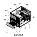
- FIG. 9 illustrates an embodiment of the coating apparatus comprising a frame 901 to accommodate all components.
- a chamber 903 in which the cleaning and the deposition steps are performed is located in the lower half of the frame.
- Valves 905 are positioned behind the chamber in the same level. Tubes connect these valves to ports at the rear of the chamber. Additional ports are provided in the chamber for sensors and electrical feedthroughs, partially shown.
- a vapor generation unit 807 is located at the upper space within the frame on top of the valves. Gas lines (not drawn) connect the vapor generation unit to other components.
- a programmable-logic-ladder (PLC) control unit 909 is positioned on the upper half space in the frame. The PLC unit runs control software.
- PLC programmable-logic-ladder
- a high voltage power supply 911 for an Ultra-violet lamp is positioned next to the PLC unit.
- control electronics 913 comprising solid state relays and an additional low voltage supply.
- a display 915 is fixed on front panel 914 .
- the display shows messages of control software and has input keys to input numbers, buttons for process control, and indicators to indicate status.
- Chamber 903 has a door 917 in the front. The door is connected to a motion support such as bearing 923 . The door is also connected to a chuck 919 for supporting the substrate to be processed.
- FIG. 10 shows the apparatus with the top plate of the chamber removed.
- an Ultra-violet (UV) lamp 1003 is above the push-in position of support chuck 919 .
- the UV lamp has grid-shape to cover most of the chuck area.
- the UV lamp is connected to the top plate (not shown) of the chamber through fixtures 1003 .
- the UV lamp is electrically connected to high-voltage power supply 911 by a feedthrough (not shown) on the chamber wall.
- Door 917 has a handle 1011 . At both sides, the door 917 is connected to rods 1005 . The rods pass through bearings 923 and are movable.
- stoppers 1007 At the end of rods 1005 , there are stoppers 1007 to limit the moving range of the rods.
- the bearings are side-mounted to outer surfaces of the chamber wall.
- Door locks 921 are also mounted to outer surface of the chamber wall.
- a contact sensor 1009 is installed in the same way to indicate whether the door is closed.
- Chuck 919 is connected to the door through a thermal isolation plate and fixture a 1015 .
- the chuck has cartridge heaters embedded into its body. The heaters are electrically connected to control electronics 913 through a feedthrough (not shown) on the chamber wall.
- Thermocouple sensors are also mounted to measure temperatures.
- FIG. 11 shows a vapor generation source comprising a body 1101 .
- a cylindrical void 1103 inside the body 1101 serves as volume to store chemical liquid and vapor.
- the void 1103 is opened on top of the body.
- a sealing cap plate 1105 with view-through window 1106 is put on upper surface of the void.
- port 1109 and port 1111 pass through the body to connect to the void.
- Port 1109 is connected to the chamber to deliver chemical vapor and port 1113 is connected to a nitrogen supply (or vice versa).
- Cartridge heaters 1117 are inserted into heater tunnels 1115 machined in the body. Heat is transferred to chemicals stored in the void through the body.
- the body may be made from chemical-resistant material, preferably stainless steel or Teflon, or, inner surface of the void may be coated with chemical-resistant material, such as Teflon.
- chemical-resistant material such as Teflon.
- nitrogen vent is first introduced to the void to protect the chemicals from ambient. Then a cap is removed for dropping in chemicals and put back after the dropping. Finally, the nitrogen is shut off for normal operation.
- Multiple sets of the same as void 1103 , cap 1105 , ports 1107 / 1111 and fitting 1109 / 1113 may exist in same body 1101 . Each set can handle one chemical without cross-interference.
- the drawing of FIG. 11 illustrates two identical chemical handling sets in the same body.
- FIG. 9 illustrates two identical units of FIG. 11 are installed as chemical generation sources. The apparatus can handle four different chemicals in one tool.
- a substrate for example a mold or wafer for imprint lithography
- a magnetic solenoid door lock 921 is electrically turned on to hold the door in position.
- a user can press a button on the display to run the process.
- the door is unlocked and pulled out to unload the substrate.
- the door shown in FIGS. 9 and 10 is manually opened and closed. It is clear that a driver source, such as motor actuator or pneumatic actuator can be installed to automatically open and close the door.
- the first step is to load mold or substrate.
- the second step is to turn on UV lamp to generate Ozone to clean mold or substrate.
- the cleaning step may take from tens seconds to several minutes.
- the third step is to turn off UV lamp and exhaust the chamber for several minutes to remove residual Ozone.
- the fourth step is to pump the chamber. Normally, a vacuum better than 1000 mTorr is needed for vapor coating. The vacuum can be reached in 30 seconds.
- the purging step typically lasts 1-3 minutes to achieve a better vacuum.
- the base vacuum of less than 50 mTorr can be achieved after 10-15 minutes pumping.
- the mold or substrate is heated to vapor coating temperature, which is typical 60-100° C.
- Surfactant contained inside the vapor generation source is heated to vapor generation temperature. Higher temperatures provide higher vapor density of surfactant.
- the vapor generation temperature is typically set at 80° C.
- the fifth step is to coat mold or substrate with surfactant vapor. The temperature that is reached in the previous step is maintained during the coating step. The coating starts with turning on control valve of vapor line. The vapor of surfactant is introduced into the chamber. The coating process on mold or substrate surface begins immediately. Coating typically takes several minutes to twenty minutes. An experimental study of 5 minutes coating deposition time showed that good surface release coating was obtained on a quartz mold.
- the vacuum pumping may be turned off to rely on good chamber seal to maintain vacuum. In such case, surfactant vapor pressure inside chamber is higher than maintaining vacuum pumping.
- the sixth step is to close vapor line to stop flow-in of surfactant vapor and pump residual vapor out of the chamber. The pumping may take several minutes to remove most of residual vapor.
- the seventh step is to vent the chamber. After the chamber is vented to atmosphere, the coated mold or substrate is unloaded. The process was performed on various mold/substrate materials, such as quartz, glass, silicon, III-IV semiconductors, and polymers.
- Surfactants that were tested include surface release surfactant (1H,1H,2H,2H-perfluorodecyltrichlorosilane) for mold treatment and surface adhesion promoter ((3-Acryloxypropyl)-trichlorosilane) for substrate treatment.
- the apparatus works for any type of surfactant, especially for surfactant having liquid phase at room temperature and higher vapor pressure at a reasonable elevated temperature.
Abstract
In imprint lithography, the mold is coated with a surface release layer for a non-sticking separation. Bonding strength of the release layer to the mold depends on the cleanness of the surface and the process of release layer deposition. In accordance with the invention, the mold is disposed in an evacuable chamber, cleaned to remove surface organic contamination and coated with the surface release layer in a chamber, all without relocation or undesired time delay. The chamber encloses a support chuck for the mold or substrate, a surface cleaner unit adjacent the support, a heating source adjacent the support, and advantageously, sensors of measuring chamber pressure, vapor partial pressure and moisture concentration. A vapor source connected to the chamber supplies release surfactant vapor. The mold is cleaned, and the cleaning is followed by vapor phase deposition of the surfactant. The mold is advantageously heated. Typical ways of cleaning include exposure to ozone or plasma ion etch. Surfactant vapor may be generated by liquid surface vaporization, liquid injection or spray vaporization. A surface adhesion promoter can be coated on the substrate by a similar method with the same apparatus.
Description
The present application claims the benefit of U.S. Provisional Patent Application Ser. No. 60/867,498 filed on Nov. 28, 2006 and U.S. Provisional Patent Application Ser. No. 60/869,981 filed on Dec. 14, 2006, all of which are herein incorporated by reference.
Not Applicable.
This invention relates to treating molds and substrates for imprint lithography, and in particular, to an integrated cleaning/deposition process and related apparatus.
Lithography is a key process in the fabrication of semiconductor integrated circuits and many optical, magnetic, biological, and electro-mechanical devices. Lithography creates a pattern on a substrate-supported moldable film so that, in subsequent process steps, the pattern can be replicated in the substrate or in another material that is added onto the substrate.
Conventional lithography, referred to as photolithography, involves applying a thin film of photosensitive resist to a substrate, exposing the resist to a desired pattern of radiation and developing the exposed resist to produce a physical pattern on the substrate. The resolution of patterns produced by photolithography is limited by the wavelength of the exposing radiation. Moreover, as pattern features become smaller, increasingly expensive shorter wavelength equipment is required.
Imprint lithography, based on a fundamentally different principle, offers high resolution, high throughput, low cost and the potential of large area coverage. In imprint lithography, a mold with a pattern of projecting and recessed features is pressed into a moldable surface, typically a thin film, deforming the shape of the film and forming a relief pattern in the film. The film is hardened, as by UV or thermal curing, and the mold and imprinted substrate are separated. After the mold is removed, the thin film can be processed, as by removing the residual reduced thickness portions to expose the underlying substrate for further processing. Imprint lithography can be used to replicate patterns having high resolution features in the microscale and nanoscale ranges. Details of nanoscale imprint lithography (“nanoimprint lithography”) are described in U.S. Pat. No. 5,772,905 issued Jun. 30, 1998 and entitled “Nanoimprint Lithography”. The '905 patent is incorporated herein by reference.
A significant factor for commercial imprint lithography is the useful life of the imprint mold. The mold lifetime directly affects cost of the products and throughput of the production. The lifetime of the imprint mold is limited by wearing of the mold surface release coating and damage to the mold material. The material damage, such as breaks, surface feature rupture, and surface indentation is caused by the stress and strain of imprinting. Wearing of the surface release coating depends on the surface chemistry, bonding strength and the coverage of the surface release layer. It is also affected by how well the release layer is applied on the mold surface. Reliable methods of applying a surface release layer are much needed for imprint lithography.
In imprint lithography, the mold is coated with a surface release layer for a non-sticking separation. Bonding strength of the release layer to the mold depends on the cleanness of the surface and the process of release layer deposition. In accordance with the invention, the mold is disposed in an evacuable chamber, cleaned to remove surface organic contamination and coated with the surface release layer in a chamber, all without relocation or undesired time delay. The chamber encloses a support chuck for the mold or substrate, a surface cleaner unit adjacent the support, a heating source adjacent the support, and advantageously, sensors for measuring chamber pressure, vapor partial pressure and moisture concentration. A vapor source connected to the chamber supplies release surfactant vapor. The mold is cleaned, and the cleaning is followed by vapor phase deposition of the surfactant. The mold is advantageously heated. Typical ways of cleaning include exposure to ozone or plasma reactive ion etch. Surfactant vapor may be generated by liquid surface vaporization, liquid injection or spray vaporization. A surface adhesion promoter can be coated on the substrate by a similar method with the same apparatus.
The advantages, nature and various additional features of the invention will appear more fully upon consideration of the illustrative embodiments now to be described in detail in connection with the accompanying drawings.
In the drawings:
It is to be understood that the drawings are to illustrate the concepts of the invention and are not to scale.
Referring to FIG. 1 , an imprint mold 100 has its molding surface covered with molecules 102 of an anti-sticking surfactant. Chemical bonds are formed between the molecules and the mold. The coverage of the molecules forms a surface release layer to provide a clean separation of the mold from the imprinted resist after imprinting. The surface release layer may be applied on the mold by any of several ways such as liquid phase immersion, vapor phase deposition, chemical vapor deposition, sputtering, and evaporation. The most widely used ways are liquid phase immersion and vapor phase deposition. Liquid phase immersion requires immersion of the mold in a liquid containing the surfactant. The molecules of the surfactant travel in the liquid and bond to the surface of the immersed mold. In vapor phase deposition, molecules of the surfactant arrive in vapor and bond to the surface of the mold when the vapor contacts with the surface. Compared to liquid phase immersion, vapor phase deposition is better in uniformity and topology coverage. Furthermore, vapor phase deposition consumes less chemical for each treatment and has no chemical waste. Therefore, vapor phase deposition is usually preferred to liquid phase immersion.
The same procedure can be used to apply an adhesion promoter (another surfactant) on the substrate to be imprinted. Thus, the method and apparatus of the invention can treat both the mold and the substrate with the same equipment and are believed effective for applying any type surfactant on a general workpiece.
In operation, mold 309 is loaded onto the chuck 305 with the molding surface of imprinting features facing upward. Cleaner 303 starts to clean the mold surface. After cleaning, and with minimal delay beyond apparatus response time, vapor deposition starts. The chamber 301 is pumped to a certain level of vacuum. Then vapor of the surfactant is introduced into the chamber from the vapor generation unit 311. The vapor partial pressure in the chamber is measured by the vapor partial pressure sensor 317. A feedback loop may be established to adjust flow-in rate of the vapor in order to control the vapor partial pressure precisely. Since typical surfactant reactions are sensitive to moisture in ambient, the moisture level in the ambient is advantageously monitored by moisture sensor 319. The moisture level may be adjusted by an additional component (not shown) which will be discussed later.
During vapor deposition, the mold may be heated by turning on the heating source 307 to speed up the surface bonding reaction and the coverage of the mold surface by surfactant molecules. After vapor deposition, the chamber is pumped to remove residual vapor. The chuck may be cooled for next run. Finally, the mold can be cooled within the chamber before or after unloading or cooled outside the chamber after unloading.
The apparatus may have a single vapor generation source or multiple vapor generation sources for multiple surfactants. In operation, vapors of surfactants may be introduced one at a time or several at a time. When several vapors are introduced, one should consider in advance acceptable cross contamination of the different surfactants.
Any of several methods may be used to precisely control the moisture level in vapor deposition. One method is to use a source of air with predetermined moisture concentration to purge the chamber. Another is to use a water vapor source to input moisture and a water absorption source to extract moisture. The moisture level in the chamber can be adjusted by controlling alternative operations of the water vapor source and the water absorption source. A third method is to use a water vapor source to input only specific amount of moisture through a flow rate controller.
Referring to FIG. 4 , in one embodiment of the apparatus, cleaner 303 may be a ultra-violet (UV) light lamp. UV lamp 403 preferably radiates very short wavelength light (<200 nm) to generate ozone at the mold surface to clean the mold. The lamp advantageously has a grid shape or a multi-tubular shape to provide strong, uniform radiation.
Referring to FIG. 5 , in another embodiment of the apparatus, cleaner 303 may comprise plasma generation electrodes. Top electrode 501 can be connected to one end of a plasma power supply through a conductive feedthrough 505. Bottom electrode 503, which can be chuck 305, may be connected to the other end of the plasma power source through a conductive feedthrough 507. When appropriate gases are mixed inside the chamber at appropriate pressure, plasma can be produced close to mold surface and chuck surface. The plasma generates ions of gas radicals that can clean the mold surface from organic contamination. The most common plasma cleaning gas is oxygen. To have uniform plasma cleaning across mold surface, the electrodes should be larger than the mold area.
One embodiment of the vapor generation source can be a gas reservoir that contains a predetermined concentration of surfactant vapor. The gas preferably comprises nitrogen, argon, helium or air. The surfactant vapor can be generated by vaporizing the surfactant and mixing it with the gas at predetermined ratio. The mixture is then filled into the reservoir. Alternatively, a user could install a prefilled reservoir as from a commercial supplier.
In addition to the port connected to the vapor generation source, the coating apparatus may have a port in chamber 301 connected to a water vapor source. Water vapor can be introduced from the source through the connection line and the port into the chamber. By selecting the amount or flow rate of water vapor introduced into the chamber, the moisture density inside the chamber can be optimally controlled for good coating strength and uniformity. Furthermore, the quality of the mold surface coating treatment can be steadily maintained by controlling the moisture density. In one embodiment, the water vapor source can be a gas reservoir that contains a predetermined moisture concentration. The gas can be air or an inert gas such as nitrogen, argon, or helium. Other embodiments of the water vapor source can be similar to the embodiments described and illustrated in FIGS. 7A , 7B and 8, where surfactant liquid 705 is replaced with pure water.
The principle of the invention can be implemented on a nanoimprint tool to clean the mold and treat it with a surface release coating on the nanoimprint tool. For such case, the described embodiments in the invention will be part of the nanoimprint tool. Through such integration, cleaning and treating the mold on site can minimally interrupt imprinting throughput by saving mold exchange time. In addition, cleaning and treating the mold can be done during the imprinting process in order to achieve higher yield and longer mold lifetime.
In operation of the apparatus, a substrate, for example a mold or wafer for imprint lithography, is loaded on to the chuck when the door is pulled out. After that, the door is pushed back against front surface of chamber wall. Then, a magnetic solenoid door lock 921 is electrically turned on to hold the door in position. After choosing and installing a program to run process, a user can press a button on the display to run the process. After the process is complete, the door is unlocked and pulled out to unload the substrate. The door shown in FIGS. 9 and 10 is manually opened and closed. It is clear that a driver source, such as motor actuator or pneumatic actuator can be installed to automatically open and close the door.
A detailed example of the operation can now be described step by step. The first step is to load mold or substrate. The second step is to turn on UV lamp to generate Ozone to clean mold or substrate. The cleaning step may take from tens seconds to several minutes. During the cleaning step, the mold or substrate may be heated to facilitate cleaning reaction. The third step is to turn off UV lamp and exhaust the chamber for several minutes to remove residual Ozone. The fourth step is to pump the chamber. Normally, a vacuum better than 1000 mTorr is needed for vapor coating. The vacuum can be reached in 30 seconds. The purging step typically lasts 1-3 minutes to achieve a better vacuum. The base vacuum of less than 50 mTorr can be achieved after 10-15 minutes pumping. During steps 3 and 4, the mold or substrate is heated to vapor coating temperature, which is typical 60-100° C. Surfactant contained inside the vapor generation source is heated to vapor generation temperature. Higher temperatures provide higher vapor density of surfactant. The vapor generation temperature is typically set at 80° C. The fifth step is to coat mold or substrate with surfactant vapor. The temperature that is reached in the previous step is maintained during the coating step. The coating starts with turning on control valve of vapor line. The vapor of surfactant is introduced into the chamber. The coating process on mold or substrate surface begins immediately. Coating typically takes several minutes to twenty minutes. An experimental study of 5 minutes coating deposition time showed that good surface release coating was obtained on a quartz mold. The vacuum pumping may be turned off to rely on good chamber seal to maintain vacuum. In such case, surfactant vapor pressure inside chamber is higher than maintaining vacuum pumping. The sixth step is to close vapor line to stop flow-in of surfactant vapor and pump residual vapor out of the chamber. The pumping may take several minutes to remove most of residual vapor. The seventh step is to vent the chamber. After the chamber is vented to atmosphere, the coated mold or substrate is unloaded. The process was performed on various mold/substrate materials, such as quartz, glass, silicon, III-IV semiconductors, and polymers. Surfactants that were tested include surface release surfactant (1H,1H,2H,2H-perfluorodecyltrichlorosilane) for mold treatment and surface adhesion promoter ((3-Acryloxypropyl)-trichlorosilane) for substrate treatment.
Examples of surfactants which can be used in the apparatus comprise perfluorohexyl-trichlorosilane, perfluorooctyl-trichlorosilane, perfluorodecyl-trichlorosilane, perfluorodecyl-trichlorosilane, perfluorohexylpropyl-trichlorosilane, perfluorodecyl-trichlorotitanium, perfluorodecyl-dichlorobromosilane, polydimethylsiloxane-trichlorosilane, perfluorodecyl-dichlorobromogermanium, perfluorodecyl-dichlorobromomochromium, acryloxypropyl-trichlorosilane, and the like. The apparatus works for any type of surfactant, especially for surfactant having liquid phase at room temperature and higher vapor pressure at a reasonable elevated temperature.
It is to be understood that the above-described embodiments are illustrative of only a few of the many possible specific embodiments which can represent applications of the invention. Numerous and varied other arrangements can be made by those skilled in the art without departing from the spirit and scope of the invention.
Claims (23)
1. A method of treating a workpiece comprising either a substrate or a mold for imprint lithography, comprising the steps of:
providing the workpiece having a surface intended for use in imprint lithography;
providing a chamber;
first, placing the workpiece within the chamber;
second, cleaning said surface of said workpiece using a chemical reaction inside said chamber to remove contamination from said surface without significantly altering said surface; and
third, without removing said cleaned workpiece to outside said chamber, sequentially depositing a layer of surfactant molecules on said surface, through vapor phase deposition inside said chamber.
2. The method of claim 1 wherein said workpiece is heated by baking within said chamber following deposition of said layer of surfactant molecules to enhance a bonding strength of said surfactant molecules to said surface.
3. The method of claim 1 wherein said surface is illuminated with ultraviolet light within said chamber, and wherein said chemical reaction comprises a reaction with ozone primarily generated by said ultraviolet light at said illuminated surface.
4. The method of claim 1 wherein said chemical reaction comprises reaction with plasma-produced radicals.
5. The method of claim 1 wherein said deposition comprises breaking of molecular chains of said surfactant molecules and connecting ends of said broken chains to the surface.
6. The method of claim 1 wherein said layer is an anti-sticking layer for imprint lithography; and
wherein said workpiece is a mold for imprint lithography.
7. The method of claim 1 wherein said layer is an adhesion promoter facilitating an adherence of material onto said workpiece; and
wherein said workpiece is a substrate for imprint lithography.
8. The method of claim 1 further including the step of establishing a desired vacuum within said chamber immediately following said cleaning step and immediately before said depositing step.
9. The method of claim 1 further including the step of activating a heater associated with said chuck during said step of cleaning, and wherein said chuck conducts thermal energy from said heater to said workpiece to heat said workpiece within said chamber during said step of cleaning.
10. The method of claim 1 further including the step of controlling an environment within said chamber between said cleaning step and said deposition step to avoid contamination of said workpiece surface.
11. The method of claim 1 wherein said chamber is a vacuum chamber.
12. The method of claim 1 further including the step of controlling a moisture level within said chamber during said deposition step.
13. The method of claim 1 further including the step of monitoring, with a moisture sensor, a moisture level within said chamber prior to said deposition step.
14. The method of claim 13 further including the step of controlling a moisture level within said chamber for said deposition step by purging said chamber with a source of air having a predetermined moisture concentration.
15. The method of claim 13 further including the step of controlling a moisture level within said chamber for said deposition step by inputting moisture into said chamber from a water vapor source.
16. The method of claim 15 wherein said moisture is input in specific quantity through a flow rate controller.
17. The method of claim 13 further including the step of controlling a moisture level within said chamber for said deposition step by extracting moisture from said chamber with a water absorption means.
18. The method of claim 13 further including the step of controlling a moisture level within said chamber for said deposition step by selectively controlling a water vapor source and a water absorption means in fluid communication with said chamber.
19. A method of treating a workpiece comprising either a substrate or a mold for imprint lithography, comprising the steps of:
providing the workpiece having a surface intended for use in imprint lithography;
providing a chamber;
first, placing the workpiece within the chamber;
second, cleaning said surface of said workpiece using a chemical reaction inside said chamber;
third, without removing said workpiece from said chamber, sequentially depositing a layer of surfactant molecules on said surface, through vapor phase deposition inside said chamber; and
wherein said workpiece is heated within said chamber before said step of cleaning.
20. The method of claim 19 wherein said surfactant molecules for deposition on said surface are generated by a single vapor generation source in fluid communication with said chamber.
21. The method of claim 19 wherein said surfactant molecules for deposition on said surface include a plurality of surfactants, generated by a plurality of vapor generation sources in fluid communication with said chamber.
22. The method of claim 19 wherein said surfactant molecules consist of at least one type of surfactant from a set of surfactants including perfluorohexyl-trichlorosilane, perfluorooctyl-trichlorosilane, perfluorodecyl-trichlorosilane, perfluorodecyl-trichlorosilane, perfluorohexylpropyl-trichlorosilane, perflurordecyl-trichlorotitanium, perfluorodecyl-dichlorobromosilane, polydimethylsiloxane-trichlorosilane, perfluorodecyl-dichlorobromogermanium, perfluorodecyl-dichlorobromomochromium, acryloxypropyl-trichlorosilane, and the like.
23. The method of claim 19 wherein said surfactant has a liquid phase at room temperature and a higher vapor pressure at an elevated temperature during said deposition phase.
Priority Applications (2)
| Application Number | Priority Date | Filing Date | Title |
|---|---|---|---|
| US11/945,470 US8337959B2 (en) | 2006-11-28 | 2007-11-27 | Method and apparatus to apply surface release coating for imprint mold |
| US13/027,530 US20110155060A1 (en) | 2006-11-28 | 2011-02-15 | Method And Apparatus To Apply Surface Release Coating For Imprint Mold |
Applications Claiming Priority (3)
| Application Number | Priority Date | Filing Date | Title |
|---|---|---|---|
| US86749806P | 2006-11-28 | 2006-11-28 | |
| US86998106P | 2006-12-14 | 2006-12-14 | |
| US11/945,470 US8337959B2 (en) | 2006-11-28 | 2007-11-27 | Method and apparatus to apply surface release coating for imprint mold |
Related Child Applications (1)
| Application Number | Title | Priority Date | Filing Date |
|---|---|---|---|
| US13/027,530 Continuation US20110155060A1 (en) | 2006-11-28 | 2011-02-15 | Method And Apparatus To Apply Surface Release Coating For Imprint Mold |
Publications (2)
| Publication Number | Publication Date |
|---|---|
| US20080131623A1 US20080131623A1 (en) | 2008-06-05 |
| US8337959B2 true US8337959B2 (en) | 2012-12-25 |
Family
ID=39476140
Family Applications (2)
| Application Number | Title | Priority Date | Filing Date |
|---|---|---|---|
| US11/945,470 Active 2029-08-01 US8337959B2 (en) | 2006-11-28 | 2007-11-27 | Method and apparatus to apply surface release coating for imprint mold |
| US13/027,530 Abandoned US20110155060A1 (en) | 2006-11-28 | 2011-02-15 | Method And Apparatus To Apply Surface Release Coating For Imprint Mold |
Family Applications After (1)
| Application Number | Title | Priority Date | Filing Date |
|---|---|---|---|
| US13/027,530 Abandoned US20110155060A1 (en) | 2006-11-28 | 2011-02-15 | Method And Apparatus To Apply Surface Release Coating For Imprint Mold |
Country Status (1)
| Country | Link |
|---|---|
| US (2) | US8337959B2 (en) |
Cited By (1)
| Publication number | Priority date | Publication date | Assignee | Title |
|---|---|---|---|---|
| US10784100B2 (en) | 2016-07-21 | 2020-09-22 | Tokyo Electron Limited | Back-side friction reduction of a substrate |
Families Citing this family (30)
| Publication number | Priority date | Publication date | Assignee | Title |
|---|---|---|---|---|
| US8846195B2 (en) * | 2005-07-22 | 2014-09-30 | Canon Nanotechnologies, Inc. | Ultra-thin polymeric adhesion layer |
| US8808808B2 (en) * | 2005-07-22 | 2014-08-19 | Molecular Imprints, Inc. | Method for imprint lithography utilizing an adhesion primer layer |
| GB0802687D0 (en) * | 2008-02-14 | 2008-03-19 | P2I Ltd | Vapour delivery system |
| TWI410288B (en) * | 2008-10-02 | 2013-10-01 | Molecular Imprints Inc | In-situ cleaning of an imprint lithography tool |
| US8394203B2 (en) * | 2008-10-02 | 2013-03-12 | Molecular Imprints, Inc. | In-situ cleaning of an imprint lithography tool |
| KR101046828B1 (en) * | 2008-10-15 | 2011-07-06 | 국민대학교산학협력단 | Apparatus and Temperature Control Method for Performing Nano-imprint Lithography with Temperature Control |
| US8361546B2 (en) * | 2008-10-30 | 2013-01-29 | Molecular Imprints, Inc. | Facilitating adhesion between substrate and patterned layer |
| TWI411656B (en) * | 2008-10-30 | 2013-10-11 | Molecular Imprints Inc | Facilitating adhesion between substrate and patterned layer |
| US20110165412A1 (en) * | 2009-11-24 | 2011-07-07 | Molecular Imprints, Inc. | Adhesion layers in nanoimprint lithograhy |
| WO2011064021A1 (en) * | 2009-11-30 | 2011-06-03 | Asml Netherlands B.V. | Imprint lithography apparatus and method |
| US8747092B2 (en) | 2010-01-22 | 2014-06-10 | Nanonex Corporation | Fast nanoimprinting apparatus using deformale mold |
| US8980751B2 (en) * | 2010-01-27 | 2015-03-17 | Canon Nanotechnologies, Inc. | Methods and systems of material removal and pattern transfer |
| JP5471514B2 (en) * | 2010-01-28 | 2014-04-16 | ウシオ電機株式会社 | Light processing equipment |
| US8524134B2 (en) * | 2010-07-12 | 2013-09-03 | Graham J. Hubbard | Method of molding polymeric materials to impart a desired texture thereto |
| TW201213591A (en) * | 2010-09-21 | 2012-04-01 | Hon Hai Prec Ind Co Ltd | Mold for making optical-film and method for manufacturing the mold |
| CN102433562A (en) * | 2010-09-29 | 2012-05-02 | 鸿富锦精密工业(深圳)有限公司 | Optical film processing die and manufacturing method thereof |
| JP5019009B2 (en) | 2010-10-29 | 2012-09-05 | 大日本印刷株式会社 | IMPRINT MOLD CLEANING METHOD, CLEANING DEVICE, AND IMPRINT MOLD MANUFACTURING METHOD |
| JP5395102B2 (en) * | 2011-02-28 | 2014-01-22 | 株式会社豊田中央研究所 | Vapor growth equipment |
| US8852693B2 (en) | 2011-05-19 | 2014-10-07 | Liquipel Ip Llc | Coated electronic devices and associated methods |
| JP5890709B2 (en) * | 2011-06-30 | 2016-03-22 | 株式会社東芝 | Template substrate and manufacturing method thereof |
| US9278857B2 (en) | 2012-01-31 | 2016-03-08 | Seagate Technology Inc. | Method of surface tension control to reduce trapped gas bubbles |
| US10105883B2 (en) | 2013-03-15 | 2018-10-23 | Nanonex Corporation | Imprint lithography system and method for manufacturing |
| US10108086B2 (en) | 2013-03-15 | 2018-10-23 | Nanonex Corporation | System and methods of mold/substrate separation for imprint lithography |
| US10182880B2 (en) | 2013-12-11 | 2019-01-22 | Caretag Surgical Aps | Attachment and cover for an electronic identification tag |
| CN105986248B (en) * | 2015-03-03 | 2018-08-28 | 北京自动化控制设备研究所 | A kind of anti-relaxation film plating process of atomic air chamber |
| US10504715B2 (en) * | 2016-07-21 | 2019-12-10 | Tokyo Electron Limited | Back-side friction reduction of a substrate |
| US10310374B2 (en) * | 2016-08-18 | 2019-06-04 | International Business Machines Corporation | Repatternable nanoimprint lithography stamp |
| KR20200083642A (en) * | 2017-11-29 | 2020-07-08 | 도쿄엘렉트론가부시키가이샤 | Reduced back friction on the substrate |
| US10453800B1 (en) | 2018-03-29 | 2019-10-22 | International Business Machines Corporation | Optical chip ID definition using nanoimprint lithography |
| CN110262186B (en) * | 2019-06-25 | 2021-12-03 | 京东方科技集团股份有限公司 | Nano-imprinting mold, nano-imprinting device and nano-imprinting method |
Citations (5)
| Publication number | Priority date | Publication date | Assignee | Title |
|---|---|---|---|---|
| US20040202865A1 (en) * | 2003-04-08 | 2004-10-14 | Andrew Homola | Release coating for stamper |
| US20050042553A1 (en) * | 2003-08-21 | 2005-02-24 | 3M Innovative Properties Company | Phototool coating |
| US20060222899A1 (en) * | 2005-03-30 | 2006-10-05 | Kabushiki Kaisha Toshiba | Magnetic recording media |
| US20070166557A1 (en) * | 2004-05-28 | 2007-07-19 | Matthias Keil | Modified metal mold for use in imprinting processes |
| US7294294B1 (en) * | 2000-10-17 | 2007-11-13 | Seagate Technology Llc | Surface modified stamper for imprint lithography |
Family Cites Families (13)
| Publication number | Priority date | Publication date | Assignee | Title |
|---|---|---|---|---|
| US3678889A (en) * | 1970-02-06 | 1972-07-25 | Tokyo Shibaura Electric Co | Reflector assembly for reflecting the vapors of high temperature volatile materials |
| US3830194A (en) * | 1972-09-28 | 1974-08-20 | Applied Materials Tech | Susceptor support structure and docking assembly |
| US4506815A (en) * | 1982-12-09 | 1985-03-26 | Thiokol Corporation | Bubbler cylinder and dip tube device |
| JPH09184080A (en) * | 1995-12-27 | 1997-07-15 | Vacuum Metallurgical Co Ltd | Formation of thin film by ultrafine grain and device therefor |
| JP2000169961A (en) * | 1998-12-02 | 2000-06-20 | Matsushita Electric Ind Co Ltd | Sputtering apparatus |
| JP2003115576A (en) * | 2001-10-03 | 2003-04-18 | Matsushita Electric Ind Co Ltd | Method for manufacturing electronic device |
| JP3881569B2 (en) * | 2002-03-13 | 2007-02-14 | 株式会社堀場エステック | Liquid material vaporizer |
| DE10297731T5 (en) * | 2002-05-08 | 2005-07-07 | Agency For Science, Technology And Research | Reverse embossing technology |
| US20050271893A1 (en) * | 2004-06-04 | 2005-12-08 | Applied Microstructures, Inc. | Controlled vapor deposition of multilayered coatings adhered by an oxide layer |
| US20050056216A1 (en) * | 2003-09-15 | 2005-03-17 | Intel Corporation | Precursor delivery system |
| US8240539B2 (en) * | 2004-05-28 | 2012-08-14 | Panasonic Corporation | Joining apparatus with UV cleaning |
| US20060219754A1 (en) * | 2005-03-31 | 2006-10-05 | Horst Clauberg | Bonding wire cleaning unit and method of wire bonding using same |
| JP4341579B2 (en) * | 2005-05-19 | 2009-10-07 | セイコーエプソン株式会社 | Microlens manufacturing method |
-
2007
- 2007-11-27 US US11/945,470 patent/US8337959B2/en active Active
-
2011
- 2011-02-15 US US13/027,530 patent/US20110155060A1/en not_active Abandoned
Patent Citations (5)
| Publication number | Priority date | Publication date | Assignee | Title |
|---|---|---|---|---|
| US7294294B1 (en) * | 2000-10-17 | 2007-11-13 | Seagate Technology Llc | Surface modified stamper for imprint lithography |
| US20040202865A1 (en) * | 2003-04-08 | 2004-10-14 | Andrew Homola | Release coating for stamper |
| US20050042553A1 (en) * | 2003-08-21 | 2005-02-24 | 3M Innovative Properties Company | Phototool coating |
| US20070166557A1 (en) * | 2004-05-28 | 2007-07-19 | Matthias Keil | Modified metal mold for use in imprinting processes |
| US20060222899A1 (en) * | 2005-03-30 | 2006-10-05 | Kabushiki Kaisha Toshiba | Magnetic recording media |
Non-Patent Citations (3)
| Title |
|---|
| Jansen et al. J. Micromech. Microeng. 6 (1996) pp. 14-28. * |
| Kao et al. IEEE transactions on Electron Devices, vol. 52 No. 8 Aug. 2005 pp. 1722-1726. * |
| Keil et al, Process development and characterization of antisticking layers on nickel-based stamps designed for nanoimprint lithography [J. Vac. Sci. Technol. B 22(6), Nov./Dec. 2004]. * |
Cited By (1)
| Publication number | Priority date | Publication date | Assignee | Title |
|---|---|---|---|---|
| US10784100B2 (en) | 2016-07-21 | 2020-09-22 | Tokyo Electron Limited | Back-side friction reduction of a substrate |
Also Published As
| Publication number | Publication date |
|---|---|
| US20080131623A1 (en) | 2008-06-05 |
| US20110155060A1 (en) | 2011-06-30 |
Similar Documents
| Publication | Publication Date | Title |
|---|---|---|
| US8337959B2 (en) | Method and apparatus to apply surface release coating for imprint mold | |
| US6328809B1 (en) | Vapor drying system and method | |
| JP5014985B2 (en) | Process processing system and method for processing substrates | |
| TW204411B (en) | ||
| JP3901156B2 (en) | Mask forming method and removing method, and semiconductor device, electric circuit, display module, color filter, and light emitting element manufactured by the method | |
| JP2008502134A (en) | Method of operating a process processing system for processing a substrate | |
| JP6263450B2 (en) | Organic monomolecular film formation method | |
| TWI293407B (en) | Substrate processing apparatus and substrate processing method | |
| TW448499B (en) | Surface treatment method and surface treatment apparatus | |
| KR100555388B1 (en) | Substrate processing apparatus and substrate processing method | |
| JP5356522B2 (en) | High throughput processing system for chemical processing and heat treatment and operation method thereof | |
| KR100797428B1 (en) | Vacuum processing apparatus and multi-chamber vacuum processing apparatus | |
| US20040226186A1 (en) | Apparatus for drying semiconductor substrates using azeotrope effect and drying method using the apparatus | |
| TW200524032A (en) | Substrate processing method, substrate processing apparatus and computer-readable recording medium | |
| TW202217457A (en) | Surface modification for metal-containing photoresist deposition | |
| US7546840B2 (en) | Method for cleaning reaction container and film deposition system | |
| KR100518147B1 (en) | Evaporation apparatus, organic material evaporation source, and method of manufacturing thin organic film | |
| US5294280A (en) | Gas measuring device and processing apparatus provided with the gas measuring device | |
| JP3954464B2 (en) | Substrate processing equipment | |
| JPH11274132A (en) | Method and device for cleaning substrate | |
| JP3989355B2 (en) | Processing apparatus and processing method | |
| JP2010212430A (en) | Atomic layer deposition apparatus | |
| JP2009099581A (en) | Etching device, and method of manufacturing non-defective layer substrate | |
| WO1998001898A1 (en) | Rie apparatus | |
| JPH1050656A (en) | Cleaning semiconductor manufacturing apparatus and semiconductor wafer and manufacturing semiconductor device |
Legal Events
| Date | Code | Title | Description |
|---|---|---|---|
| AS | Assignment |
Owner name: NANONEX CORPORATION, NEW JERSEY Free format text: ASSIGNMENT OF ASSIGNORS INTEREST;ASSIGNORS:ZHANG, WEI, MR.;HU, LIN, MR.;TAN, HUA, MR.;AND OTHERS;SIGNING DATES FROM 20101217 TO 20110225;REEL/FRAME:026195/0063 |
|
| STCF | Information on status: patent grant |
Free format text: PATENTED CASE |
|
| FPAY | Fee payment |
Year of fee payment: 4 |
|
| MAFP | Maintenance fee payment |
Free format text: PAYMENT OF MAINTENANCE FEE, 8TH YR, SMALL ENTITY (ORIGINAL EVENT CODE: M2552); ENTITY STATUS OF PATENT OWNER: SMALL ENTITY Year of fee payment: 8 |