US8330352B2 - Organic light emitting diode display and method for manufacturing the same - Google Patents
Organic light emitting diode display and method for manufacturing the same Download PDFInfo
- Publication number
- US8330352B2 US8330352B2 US12/250,225 US25022508A US8330352B2 US 8330352 B2 US8330352 B2 US 8330352B2 US 25022508 A US25022508 A US 25022508A US 8330352 B2 US8330352 B2 US 8330352B2
- Authority
- US
- United States
- Prior art keywords
- pixels
- pixel
- light emitting
- organic light
- emitting device
- Prior art date
- Legal status (The legal status is an assumption and is not a legal conclusion. Google has not performed a legal analysis and makes no representation as to the accuracy of the status listed.)
- Active, expires
Links
Images


Classifications
-
- G—PHYSICS
- G09—EDUCATION; CRYPTOGRAPHY; DISPLAY; ADVERTISING; SEALS
- G09G—ARRANGEMENTS OR CIRCUITS FOR CONTROL OF INDICATING DEVICES USING STATIC MEANS TO PRESENT VARIABLE INFORMATION
- G09G3/00—Control arrangements or circuits, of interest only in connection with visual indicators other than cathode-ray tubes
- G09G3/20—Control arrangements or circuits, of interest only in connection with visual indicators other than cathode-ray tubes for presentation of an assembly of a number of characters, e.g. a page, by composing the assembly by combination of individual elements arranged in a matrix no fixed position being assigned to or needed to be assigned to the individual characters or partial characters
- G09G3/22—Control arrangements or circuits, of interest only in connection with visual indicators other than cathode-ray tubes for presentation of an assembly of a number of characters, e.g. a page, by composing the assembly by combination of individual elements arranged in a matrix no fixed position being assigned to or needed to be assigned to the individual characters or partial characters using controlled light sources
- G09G3/30—Control arrangements or circuits, of interest only in connection with visual indicators other than cathode-ray tubes for presentation of an assembly of a number of characters, e.g. a page, by composing the assembly by combination of individual elements arranged in a matrix no fixed position being assigned to or needed to be assigned to the individual characters or partial characters using controlled light sources using electroluminescent panels
- G09G3/32—Control arrangements or circuits, of interest only in connection with visual indicators other than cathode-ray tubes for presentation of an assembly of a number of characters, e.g. a page, by composing the assembly by combination of individual elements arranged in a matrix no fixed position being assigned to or needed to be assigned to the individual characters or partial characters using controlled light sources using electroluminescent panels semiconductive, e.g. using light-emitting diodes [LED]
- G09G3/3208—Control arrangements or circuits, of interest only in connection with visual indicators other than cathode-ray tubes for presentation of an assembly of a number of characters, e.g. a page, by composing the assembly by combination of individual elements arranged in a matrix no fixed position being assigned to or needed to be assigned to the individual characters or partial characters using controlled light sources using electroluminescent panels semiconductive, e.g. using light-emitting diodes [LED] organic, e.g. using organic light-emitting diodes [OLED]
-
- H—ELECTRICITY
- H10—SEMICONDUCTOR DEVICES; ELECTRIC SOLID-STATE DEVICES NOT OTHERWISE PROVIDED FOR
- H10K—ORGANIC ELECTRIC SOLID-STATE DEVICES
- H10K59/00—Integrated devices, or assemblies of multiple devices, comprising at least one organic light-emitting element covered by group H10K50/00
- H10K59/30—Devices specially adapted for multicolour light emission
- H10K59/35—Devices specially adapted for multicolour light emission comprising red-green-blue [RGB] subpixels
- H10K59/352—Devices specially adapted for multicolour light emission comprising red-green-blue [RGB] subpixels the areas of the RGB subpixels being different
-
- H—ELECTRICITY
- H10—SEMICONDUCTOR DEVICES; ELECTRIC SOLID-STATE DEVICES NOT OTHERWISE PROVIDED FOR
- H10K—ORGANIC ELECTRIC SOLID-STATE DEVICES
- H10K59/00—Integrated devices, or assemblies of multiple devices, comprising at least one organic light-emitting element covered by group H10K50/00
- H10K59/30—Devices specially adapted for multicolour light emission
- H10K59/35—Devices specially adapted for multicolour light emission comprising red-green-blue [RGB] subpixels
- H10K59/353—Devices specially adapted for multicolour light emission comprising red-green-blue [RGB] subpixels characterised by the geometrical arrangement of the RGB subpixels
-
- G—PHYSICS
- G09—EDUCATION; CRYPTOGRAPHY; DISPLAY; ADVERTISING; SEALS
- G09G—ARRANGEMENTS OR CIRCUITS FOR CONTROL OF INDICATING DEVICES USING STATIC MEANS TO PRESENT VARIABLE INFORMATION
- G09G2300/00—Aspects of the constitution of display devices
- G09G2300/04—Structural and physical details of display devices
- G09G2300/0439—Pixel structures
- G09G2300/0452—Details of colour pixel setup, e.g. pixel composed of a red, a blue and two green components
-
- H—ELECTRICITY
- H10—SEMICONDUCTOR DEVICES; ELECTRIC SOLID-STATE DEVICES NOT OTHERWISE PROVIDED FOR
- H10K—ORGANIC ELECTRIC SOLID-STATE DEVICES
- H10K71/00—Manufacture or treatment specially adapted for the organic devices covered by this subclass
- H10K71/10—Deposition of organic active material
- H10K71/16—Deposition of organic active material using physical vapour deposition [PVD], e.g. vacuum deposition or sputtering
- H10K71/166—Deposition of organic active material using physical vapour deposition [PVD], e.g. vacuum deposition or sputtering using selective deposition, e.g. using a mask
Definitions
- the present invention relates to an organic light emitting device and a method for manufacturing the same.
- LCD liquid crystal display
- CRTs cathode ray tubes
- the LCD is a passive display device, an additional back-light is added as a light source. Also, the LCD may have various problems such as a slow response time and a narrow viewing angle.
- organic light emitting device organic light emitting diode display, OLED display
- OLED display organic light emitting diode display
- the organic light emitting device includes two electrodes and an organic light emitting layer interposed between the two electrodes.
- One of the electrodes injects holes into the light emitting layer and the other injects electrons.
- the injected electrons and holes combine to form excitons, which emit light as they discharge energy.
- Emission layers for displaying red, green, and blue colors may be used to display full colors, and the same color emission layers may be arranged in rows of stripes.
- Emission layers having the stripe structure may be formed using a shadow mask.
- the shadow mask includes a plurality of openings having substantially the same size and shape as the emission layers, and an organic material is deposited through the openings such that the plurality of emission layers arranged in a row may be simultaneously formed.
- This invention provides an organic light emitting display device that may have an increased aperture ratio.
- the present invention discloses an organic light emitting device including a plurality of first pixels including a first pixel electrode and an emission layer disposed on the first pixel electrode to display a first color; a plurality of second pixels including a second pixel electrode and an emission layer disposed on the second pixel electrode to display a second color; and a plurality of third pixels including a third pixel electrode and an emission layer disposed on the third pixel electrode to display a third color.
- the first and second pixels are arranged in a first column, the third pixels are arranged in a second column, and the emission layer of the third pixels overlaps at least two third pixel electrodes.
- the present invention also discloses an organic light emitting device including a plurality of first pixels including an emission layer to display a first color; a plurality of second pixels including an emission layer to display a second color; and a plurality of third pixels including an emission layer to display a third color.
- the first and second pixels are arranged in a first column, the third pixels are arranged in a second column, and the emission layers of at least two third pixels are connected to each other.
- the present invention also discloses an organic light emitting device including a plurality of red pixel groups arranged in a 2 ⁇ 2 matrix of four red pixels sharing one red emission layer; a plurality of green pixel groups arranged in a 2 ⁇ 2 matrix of four green pixels sharing one green emission layer; and a plurality of blue pixel groups arranged in a 2 ⁇ 2 matrix of four blue pixels sharing one blue emission layer.
- the red pixel groups and the green pixel groups are alternately arranged in a first column, the blue pixel groups are continuously arranged in a second column, and the first column and the second column are alternately arranged.
- the present invention also discloses an organic light emitting device including a plurality of first, second, and third pixels to display different colors.
- the first and second pixels are arranged in a first column
- the third pixels are arranged in a second column
- an interval between neighboring third pixels is larger than an interval between neighboring first and second pixels.
- the present invention also discloses a method for manufacturing an organic light emitting device that includes forming a plurality of pixel electrodes on a substrate; forming a plurality of first, second, and third emission layers for respectively emitting light of first, second, and third colors on the pixel electrodes; and forming a common electrode on the first, second, and third emission layers.
- Forming the first, second, and third emission layers includes forming the first emission layers by using a first mask including a plurality of first openings, forming the second emission layers on positions neighboring the first emission layers by using the first mask, and forming the third emission layers on positions neighboring the first and second emission layers by using a second mask including a plurality of second openings having a different size from the first openings.
- the present invention also discloses a method for manufacturing an organic light emitting device that includes forming a plurality of pixel electrodes on a substrate; forming a plurality of emission layers on the pixel electrodes; and forming a common electrode on the emission layers.
- Forming the emission layers includes sequentially forming a plurality of first, second, and third emission layers that display different colors, and at least one of the first, the second, and the third emission layers overlaps at least two neighboring pixel electrodes.
- FIG. 1 is a top plan view schematically showing the arrangement of a plurality of pixels in an organic light emitting device according to an exemplary embodiment of the present invention.
- FIG. 2 is a cross-sectional view schematically showing a red pixel R, a green pixel G, and a blue pixel B taken along lines II-II′, II′-II′′, and II′′-II′′′ shown in FIG. 1 .
- FIG. 3A and FIG. 3B are schematic diagrams showing a mask for forming an organic emission layer in a manufacturing method of an organic light emitting device according to an exemplary embodiment of the present invention.
- FIG. 4A , FIG. 4B , and FIG. 4C are schematic diagrams sequentially showing methods for forming the organic emission layer in the manufacturing method of the organic light emitting device shown in FIG. 1 and FIG. 2 according to an exemplary embodiment of the present invention.
- FIG. 5 is a cross-sectional view taken along line V-V shown in FIG. 4A .
- FIG. 6 is a top plan view schematically showing the arrangement of a plurality of pixels in an organic light emitting device of a stripe structure.
- FIG. 7 is a schematic diagram showing a mask for forming an organic emission layer in an organic light emitting device of a stripe structure.
- FIG. 8A , FIG. 8B , and FIG. 8C are schematic diagrams sequentially showing methods for forming the organic emission layer of a stripe structure in a manufacturing method of an organic light emitting device.
- FIG. 9 is a cross-sectional view taken along line IX-IX shown in FIG. 8A .
- FIG. 10 is a top plan view schematically showing the arrangement of a plurality of pixels in an organic light emitting device according to another exemplary embodiment of the present invention.
- FIG. 11 is a cross-sectional view schematically showing a red pixel R, a green pixel G, and a blue pixel B taken along lines XI-XI′, XI′-XI′′, and XI′′-XI′′′ shown in FIG. 10 .
- FIG. 12A and FIG. 12B are schematic diagrams showing a mask for forming an organic emission layer in a manufacturing method of an organic light emitting device according to another exemplary embodiment of the present invention.
- FIG. 13A , FIG. 13B , and FIG. 13C are schematic diagrams sequentially showing methods for forming the organic emission layer in the manufacturing method of the organic light emitting device shown in FIG. 10 and FIG. 11 according to another exemplary embodiment of the present invention.
- FIG. 14 is a top plan view schematically showing the arrangement of a plurality of pixels in an organic light emitting device according to another exemplary embodiment of the present invention.
- FIG. 15 is a cross-sectional view schematically showing a red pixel R, a green pixel G, and a blue pixel B taken along lines XV-XV′ and XV′-XV′′ shown in FIG. 14
- FIG. 16A and FIG. 16B are schematic diagrams showing a mask for forming an organic emission layer in a manufacturing method of an organic light emitting device according to another exemplary embodiment of the present invention.
- FIG. 17A , FIG. 17B , and FIG. 17C are schematic diagrams sequentially showing methods for forming the organic emission layer in the manufacturing method of the organic light emitting device shown in FIG. 14 and FIG. 15 according to another exemplary embodiment of the present invention.
- FIG. 18 is a top plan view schematically showing the arrangement of a plurality of pixels in an organic light emitting device according to another exemplary embodiment of the present invention.
- FIG. 19 is a top plan view schematically showing the arrangement of a plurality of pixels in an organic light emitting device according to another exemplary embodiment of the present invention.
- FIG. 20 is a graph showing the aperture ratios of the organic light emitting device according to an exemplary embodiment of the present invention, and the organic light emitting device of the stripe structure.
- FIG. 1 is a top plan view schematically showing the arrangement of a plurality of pixels in an organic light emitting device according to an exemplary embodiment of the present invention
- FIG. 2 is a cross-sectional view taken along lines II-II′, II′-II′′, and II′′-II′′′ of FIG. 1 .
- an organic light emitting device includes red pixels R to display a red color, green pixels G to display a green color, and blue pixels B to display a blue color.
- the red pixels R, the green pixels G, and the blue pixels B form the basic pixel, which is used to display full colors, and three pixels forming one group are repeated according to a row and column.
- the plurality of red pixels R and the plurality of green pixels G are alternately arranged in a first column, and the plurality of blue pixels B are continuously arranged in a second column.
- red pixels R and the blue pixels B are alternately arranged in a row
- green pixels G and the blue pixels B are also alternately arranged in a row.
- neither the red pixels R, the green pixels G, nor the blue pixels B are continuously arranged in a line in the column or row directions.
- intervals b between neighboring blue pixels B are larger than intervals a between neighboring red pixels R and green pixels G.
- the intervals a between the red pixels R and the green pixels G are substantially the same as the intervals a between the red pixels R and the blue pixels B and the green pixels G and the blue pixels B.
- the red pixels R and the green pixels G have substantially the same area, and the blue pixels B may have a larger area than the areas of the red pixels R and the green pixels G.
- the red pixel R and the green pixel G are disposed at the left side and the blue pixel B is disposed at the right side such that the area ratio may be controlled.
- the arrangement of the pixels may vary.
- the blue pixels B are larger than the red pixels R and the green pixels G to compensate for the blue emission layer, which has lower emitting efficiency and a shorter lifetime than the red and green emission layers.
- the luminance of the red, green, and blue pixels R, G, and B may be more uniform.
- the organic light emitting device includes a plurality of pixel electrodes 191 R, 191 G, and 191 B, a plurality of organic emission layers 370 R, 370 G, and 370 B, and a common electrode 270 , which are formed on a substrate 110 .
- the pixel electrodes 191 R, 191 G, and 191 B, the organic emission layers 370 R, 370 G, and 370 B, and the common electrode 270 form organic light emitting diodes (OLED).
- An insulating layer 361 for insulation between the pixel electrodes 191 R, 191 G, and 191 B and the common electrode 270 , may be included, and while not shown in the drawing, a plurality of signal lines including a plurality of gate lines, a plurality of data lines, and a plurality of driving voltage lines, a plurality of switching transistors connected to the gate lines and the data lines, and a plurality of driving transistors connected to the driving voltage lines, the switching transistors, and the pixel electrodes 191 R, 191 G, and 191 B, may be further included.
- FIG. 1 and FIG. 2 A method for manufacturing the organic light emitting device shown in FIG. 1 and FIG. 2 will be described in detail below with reference to FIG. 3A , FIG. 3B , FIG. 4A , FIG. 4B , FIG. 4C , and FIG. 5 , as well as FIG. 1 and FIG. 2 .
- FIG. 3A and FIG. 3B are schematic diagrams showing masks for forming an organic emission layer in a manufacturing method of an organic light emitting device according to an exemplary embodiment of the present invention
- FIG. 4A , FIG. 4B , and FIG. 4C are schematic diagrams sequentially showing methods for forming the organic emission layer in the manufacturing method of the organic light emitting device shown in FIG. 1 and FIG. 2 according to an exemplary embodiment of the present invention
- FIG. 5 is a cross-sectional view taken along line V-V shown in FIG. 4A .
- a plurality of pixel electrodes 191 R, 191 G, and 191 B are formed on the insulation substrate 110 , and the insulating layer 361 is deposited thereon.
- the insulating layer 361 has a plurality of openings 365 exposing the pixel electrodes 191 R, 191 G, and 191 B.
- emission layers 370 R, 370 G, and 370 B are formed in respective openings 365 .
- the emission layers 370 R, 370 G, and 370 B may be formed through a deposition method using a shadow mask.
- the first mask 10 includes a plurality of openings 10 a having an approximately square shape
- the second mask 20 includes a plurality of openings 20 a having an approximately rectangular shape.
- the openings 20 a have a larger area than the openings 10 a.
- the first mask 10 is disposed on the substrate 110 including the pixel electrodes 191 R, 191 G, and 191 B and the insulating layer 361 .
- a red emission material is deposited through the openings 10 a of the first mask 10 to form a plurality of red emission layers 370 R on the pixel electrodes 191 R.
- the first mask 10 is then moved a predetermined distance, and a green emission material is deposited through the openings 10 a of the first mask 10 to form a plurality of green emission layers 370 G on the pixel electrodes 191 G.
- the second mask 20 is disposed on the substrate 110 , and a blue emission material is deposited through the openings 20 a of the second mask 20 to form a plurality of blue emission layer 370 B on the pixel electrodes 191 B.
- the red emission layers 370 R and the green emission layers 370 G are formed using the first mask 10
- the blue emission layers 370 B are formed using the second mask 20 .
- the red emission layers 370 R and the green emission layers 370 G are alternately arranged in a first column, and the blue emission layers 370 B are continuously arranged in a second column that is adjacent to the first column. Also, the interval b between neighboring blue emission layers 370 B is larger than the interval a between the red emission layers 370 R and the green emission layers 370 G.
- the organic emission layers are formed using masks including sufficient intervals between openings to form the above-described pixel arrangement.
- masks including sufficient intervals between openings spaces between the openings may be manufactured such that the organic material may be precisely deposited on the portions where the edges of the openings meet each other when depositing the organic material through the openings.
- the organic emission layer may be formed to have the same size as the openings of the mask, the emission area and the aperture ratio may be improved.
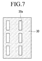
- the organic light emitting device including the stripe structure and a method for manufacturing the same will be described in detail below with reference to FIG. 6 , FIG. 7 , FIG. 8A , FIG. 8B , FIG. 8C , and FIG. 9 .
- FIG. 6 is a top plan view schematically showing the arrangement of a plurality of pixels in an organic light emitting device of a stripe structure
- FIG. 7 is a schematic diagram showing a mask for forming an organic emission layer in an organic light emitting device of a stripe structure
- FIG. 8A , FIG. 8B , and FIG. 8C are schematic diagrams sequentially showing methods for forming of the organic emission layer in the manufacturing method of the organic light emitting device of a stripe structure
- FIG. 9 is a cross-sectional view taken along line IX-IX shown in FIG. 8A .
- an organic light emitting device of the stripe structure includes a plurality of red pixels R arranged in a first column, a plurality of green pixels G arranged in a second column, and a plurality of blue pixels B arranged in a third column.
- a red pixel R, a green pixel G, and a blue pixel B arranged in the row direction form one group.
- FIG. 7 A manufacturing method of the organic light emitting device will be described with reference to FIG. 7 , FIG. 8A , FIG. 8B , FIG. 8C , and FIG. 9 .
- one mask 30 may be used to deposit the emission layers in the organic light emitting device of the stripe structure. That is, because the red, green, and blue emission layers 370 R, 370 G, and 370 B have the same shape and size, they may be formed using the same mask 30 .
- the mask 30 includes a plurality of openings 30 a having a substantially rectangular shape, and the openings 30 a are arranged with narrower intervals than those of the openings 10 a and 20 a of the masks 10 and 20 according to an exemplary embodiment of the present invention.
- the third mask 30 is disposed on the substrate 110 including the pixel electrodes 191 R and the insulating layer 361 .
- a red emission material is deposited through the openings 30 a of the third mask 30 to form a red emission layer 370 R on the pixel electrodes 191 R.
- the third mask 30 is moved a predetermined distance, and a green emission material is deposited through the openings 30 a of the third mask 30 to form a green emission layer 370 G on the pixel electrodes 191 G.
- the third mask 30 is then again moved a predetermined distance, and a blue emission material is deposited through the openings 30 a of the third mask 30 to form a blue emission layer 370 B on the pixel electrodes 191 B.
- one mask 30 moves three times to form the red, green, and blue emission layers 370 R, 370 G, and 370 B.
- the intervals between the openings 30 a of the mask 30 are narrow, it may be difficult to minutely manufacture the edges of the openings when manufacturing the mask.
- the edge portions of the opening may not be minutely formed.
- the side surfaces of the opening may have an uneven shape.
- a shadow effect in which the organic material is not deposited on portions 15 a and 15 b corresponding to the edges of the openings, may be generated such that the area where the organic material is deposited is reduced. Accordingly, the organic emission layer is actually formed with a smaller area than the size of the opening. Consequently, the emission area and the aperture ratio are reduced.
- the deposition area of the organic emission layer formed according to an exemplary embodiment of the present invention is larger than the deposition area of the organic emission layer formed in the organic light emitting device of the stripe structure, the emission area and the aperture ratio may be increased.
- FIG. 10 is a top plan view schematically showing the arrangement of a plurality of pixels in an organic light emitting device according to the present exemplary embodiment of the present invention
- FIG. 11 is a cross-sectional view schematically showing a red pixel R, a green pixel G, and a blue pixel B taken along lines XI-XI′, XI′-XI′′, and XI′′-XI′′′ shown in FIG. 10 .
- the plurality of red pixels R and the plurality of green pixels G are alternately arranged in a first column, and the plurality of blue pixels B are continuously arranged in a second column, like the above-described embodiment.
- red pixels R and the blue pixels B are alternately arranged in a row
- green pixels G and the blue pixels B are also alternately arranged in a row.
- the intervals d between the red pixels R and the green pixels G are the same as the interval between the red pixels R and the blue pixels B, and between the green pixels G and the blue pixels B. Also, two neighboring blue pixels B 1 and B 2 form one blue pixel group, and the interval f between two neighboring blue pixel groups is larger than the interval d between the red pixels R and the green pixels G.
- the emission layers of two neighboring blue pixels B 1 and B 2 are formed of one pattern. That is, in this exemplary embodiment, the emission layers 370 B of the blue pixels B overlap two neighboring pixel electrodes 191 B 1 and 191 B 2 .
- the red emission layer 370 R is formed on the pixel electrode 191 R in the red pixel R
- the green emission layer 370 G is formed on the pixel electrode 191 G in the green pixel G.
- the emission layer 370 B of the first and second blue pixels B 1 and B 2 which are neighboring blue pixels in the column of the blue pixels, is formed of one pattern.
- one portion of the blue emission layer 370 B is the emission layer 370 B 1 of the first blue pixel B 1
- another portion of the blue emission layer 370 B is the emission layer 370 B 2 of the second blue pixel B 2 .
- a shadow mask having an opening with a size corresponding to the sum of the emission areas of the first and second blue pixels B 1 and B 2 may be used, and will be described below in detail.
- the emission layer 370 B of two neighboring blue pixels B 1 and B 2 is formed of one pattern such that they are connected without an interval therebetween, and the interval between two neighboring first and second blue pixels B 1 and B 2 is substantially determined by the interval e between the pixel electrode 191 B 1 of the first blue pixel B 1 and the pixel electrode 191 B 2 of the second blue pixel B 2 .
- the interval e between the pixel electrode 191 B 1 and the pixel electrode 191 B 2 is unrelated to the shadow mask, which is used to deposit the emission layer 370 B, such that the shadow effect, in which the emission area is reduced by the limits of the shadow mask, may be prevented.
- FIG. 10 and FIG. 11 A method for manufacturing the organic light emitting device shown in FIG. 10 and FIG. 11 will be described in detail below with reference to FIG. 12A , FIG. 12B , FIG. 13A , FIG. 13B , and FIG. 13C , as well as FIG. 10 and FIG. 11 .
- FIG. 12A and FIG. 12B are schematic diagrams showing masks for forming an organic emission layer in a manufacturing method of an organic light emitting device according to the current exemplary embodiment of the present invention
- FIG. 13A , FIG. 13B , and FIG. 13C are schematic diagrams sequentially showing methods for forming of the organic emission layer in the manufacturing method of the organic light emitting device shown in FIG. 10 and FIG. 11 .
- a plurality of pixel electrodes 191 R, 191 G, 191 B 1 , and 191 B 2 are formed on an insulation substrate 110 , and an insulating layer 361 is deposited thereon.
- the insulating layer 361 has a plurality of openings 365 exposing the pixel electrodes 191 R, 191 G, 191 B 1 , and 191 B 2 .
- emission layers 370 R, 370 G, and 370 B are formed in respective openings 365 .
- the emission layers 370 R, 370 G, and 370 B may be formed through a deposition method using a shadow mask.
- the fourth mask 40 includes a plurality of openings 40 a having an approximately square shape, and it may be the same as the first mask 10 used to form the red emission layers 370 R and the green emission layers 370 G in the previous exemplary embodiment.
- the fifth mask 50 includes a plurality of openings 50 a having an approximately rectangular shape. The openings 50 a have a larger area than the openings 40 a.
- the fourth mask 40 is disposed on the substrate 110 including the pixel electrodes 191 R, 191 G, 191 B 1 , and 191 B 2 , and the insulating layer 361 .
- a red emission material is deposited through the openings 40 a of the fourth mask 40 to form a plurality of red emission layers 370 R on the pixel electrodes 191 R, like the above-described embodiment.
- the fourth mask 40 is moved a predetermined distance, and a green emission material is deposited through the openings 40 a of the first mask 40 to form a plurality of green emission layers 370 G on the pixel electrodes 191 G.
- the fifth mask 50 is then disposed on the substrate 110 , and a blue emission material is deposited through the openings 50 a of the second mask 50 to form a plurality of blue emission layers 370 B on the pixel electrodes 191 B 1 and 191 B 2 .
- the blue emission layers 370 B overlap the two pixel electrodes 191 B 1 and 191 B 2 .
- the red emission layers 370 R and the green emission layers 370 G are formed using the fourth mask 40 , and two neighboring blue emission layers 370 B 1 and 370 B 2 are formed in one pattern using the fifth mask 50 .
- the organic emission layers are formed through the above-described method such that they may be formed using a mask including sufficient intervals between openings to form the above-described pixel arrangement.
- the spaces between the openings may be minutely manufactured such that the organic material is precisely deposited to the portions where the edges of the openings meet each other when depositing the organic material through the openings.
- the organic emission layer of two neighboring blue pixels is formed in one pattern such that a shadow effect generated by limits of the shadow mask of the case in which the emission layers are separately formed may be prevented. Accordingly, reduction of the emission area and the aperture ratio by the interval between the emission layers may be prevented.
- FIG. 14 is a top plan view schematically showing the arrangement of a plurality of pixels in an organic light emitting device according to another exemplary embodiment of the present invention
- FIG. 15 is a cross-sectional view schematically showing a red pixel R, a green pixel G, and a blue pixel B taken along lines XV-XV′ and XV′-XV′′ shown in FIG. 14 .
- the plurality of red pixels R and the plurality of blue pixels B are alternately arranged in a row, and the plurality of green pixels G and the plurality of blue pixels B are also alternately arranged in a row, like the above-described embodiment.
- the intervals g between the red pixels R and the green pixels G, between the red pixels R and the blue pixels B, and between the green pixels G and the blue pixels B are substantially the same.
- the interval i between two neighboring blue pixel groups is larger than the interval g.
- the red pixels R and the green pixels G are repeatedly disposed by twos in the column direction.
- the emission layers 370 B of two neighboring blue pixels B 1 and B 2 are formed of one pattern in the column direction
- the emission layers 370 R of two neighboring red pixels R 1 and R 2 and/or the emission layers 370 G of two neighboring green pixels G 1 and G 2 are each formed of one pattern.
- a portion of the blue emission layer 370 B is the emission layer 370 B 1 of the first blue pixel B 1 and another portion of the blue emission layer 370 B is the emission layer 370 B 2 of the second blue pixel B 2
- a portion of the red emission layer 370 R is the emission layer 370 R 1 of the first red pixel R 1 and another portion of the red emission layer 370 R is the emission layer 370 R 2 of the second red pixel R 2
- a portion of the green emission layer 370 G is the emission layer 370 G 1 of the first green pixel G 1 and another portion of the green emission layer 370 G is the emission layer 370 G 2 of the second green pixel G 2 .
- a shadow mask having openings with a size corresponding to the sum of the emission areas of neighboring first and second red pixels R 1 and R 2 , or neighboring first and second green pixels G 1 and G 2 , may be used.
- the emission layer 370 R of two neighboring red pixels R 1 and R 2 is formed of one pattern such that they are connected without an interval therebetween, and the interval between neighboring first and second red pixels R 1 and R 2 is substantially determined by the interval h between the pixel electrodes 191 R 1 of the first red pixel R 1 and the pixel electrode 191 R 2 of the second red pixel R 2 .
- the emission layer 370 G of two neighboring green pixels G 1 and G 2 is formed of one pattern such that they are connected without an interval therebetween, and the interval between two neighboring first and second green pixels G 1 and G 2 is substantially determined by the interval h between the pixel electrodes 191 G 1 of the first green pixel G 1 and the pixel electrode 191 G 2 of the second green pixel G 2 .
- the interval h between the pixel electrode 191 R 1 and the pixel electrode 191 R 2 or the pixel electrode 191 G 1 and the pixel electrode 191 G 2 is unrelated to the shadow mask used to deposit the emission layer 370 R and 370 G such that the shadow effect, in which the emission area is reduced by the limits of the shadow mask, may be prevented.
- FIG. 14 and FIG. 15 A method for manufacturing the organic light emitting device shown in FIG. 14 and FIG. 15 will be described in detail below with reference to FIG. 16A , FIG. 16B , FIG. 17A , FIG. 17B , and FIG. 17C , as well as FIG. 14 and FIG. 15 .
- FIG. 16A and FIG. 16B are schematic diagrams showing a mask for forming an organic emission layer in a manufacturing method of an organic light emitting device according to the current exemplary embodiment of the present invention
- FIG. 17A , FIG. 17B , and FIG. 17C are schematic diagrams sequentially showing methods for forming the organic emission layer in the manufacturing method of the organic light emitting device shown in FIG. 14 and FIG. 15 .
- a plurality of pixel electrodes 191 R 1 , 191 R 2 , 191 G 1 , 191 G 2 , 191 B 1 , and 191 B 2 are formed on an insulation substrate 110 , and an insulating layer 361 is deposited thereon.
- the insulating layer 361 has a plurality of openings 365 exposing the pixel electrodes 191 R 1 , 191 R 2 , 191 G 1 , 191 G 2 , 191 B 1 , and 191 B 2 .
- emission layers 370 R, 370 G, and 370 B are formed in respective openings 365 .
- the emission layers 370 R, 370 G, and 370 B may be formed through a deposition method using a shadow mask.
- the sixth mask 60 includes a plurality of openings 60 a having an approximately rectangular shape, and it is used to deposit the red emission layers 370 R and the green emission layers 370 G
- the fifth mask 50 includes a plurality of openings 50 a having an approximately rectangular shape, and it is used to deposit the blue emission layer 370 B.
- the sixth mask 60 is disposed on the substrate 110 including the pixel electrodes 191 R 1 , 191 R 2 , 191 G 1 , 191 G 2 , 191 B 1 , and 191 B 2 , and the insulating layer 361 .
- a red emission material is deposited through the openings 60 a of the sixth mask 60 to form a plurality of red emission layers 370 R on the pixel electrodes 191 R 1 and 191 R 2 .
- the red emission layers 370 R overlap two pixel electrodes 191 R 1 and 191 R 2 .
- the sixth mask 60 is moved a predetermined distance on the substrate 110 , and a green emission material is deposited through the openings 60 a of the sixth mask 60 to form a plurality of green emission layers 370 G on the pixel electrodes 191 G 1 and 191 G 2 .
- the green emission layers 370 G overlap two pixel electrodes 191 G 1 and 191 G 2 .
- the fifth mask 50 is disposed on the substrate 110 , and a blue emission material is deposited through the openings 50 a of the fifth mask 50 to form a plurality of blue emission layers 370 B on the pixel electrodes 191 B 1 and 191 B 2 .
- the blue emission layers 370 B overlap two pixel electrodes 191 B 1 and 191 B 2 .
- the red emission layer 370 R and the green emission layer 370 G of two neighboring red and green pixels, respectively, are formed in one pattern, as is the blue emission layer 370 B. Accordingly, reduction of the emission area by manufacturing limits of a shadow mask may be prevented for the red pixel R and the green pixel G, as in blue pixel B, such that the emission area and the aperture ratio may be increased in the red pixel R and the green pixel G.
- FIG. 18 is a top plan view schematically showing the arrangement of a plurality of pixels in an organic light emitting device according to another exemplary embodiment of the present invention.
- the red pixels R and the green pixels G are repeatedly arranged by twos in a first column, as in the third embodiment, and the blue pixels B are continuously arranged in the second column.
- the red pixels R and the blue pixels B are repeatedly arranged by twos in a row, and the green pixels G and the blue pixels B are repeatedly arranged by twos in a row.
- red pixels R, four blue pixels B, and four green pixels G respectively form groups such that the blue emission layer 370 B of four neighboring blue pixels B 1 , B 2 , B 3 , and B 4 is formed of one pattern, the red emission layer 370 R of four neighboring red pixels R 1 , R 2 , R 3 , and R 4 is formed of one pattern, and the green emission layer 370 G of four neighboring green pixels G 1 , G 2 , G 3 , and G 4 is formed of one pattern.
- the interval j between the red pixel group including four red pixels R and the green pixel group including four green pixels G, the interval j between the red pixel group and the blue pixel group including four blue pixels B, and the interval j between the green pixel group and the blue pixel group are substantially the same.
- the interval m between two neighboring blue pixel groups is larger than the interval j between the red pixel group and the green pixel group.
- one emission layer is formed in four neighboring pixels such that a shadow mask having an opening with a size corresponding to the sum of the emission areas of the four neighboring pixels may be used when forming the emission layer.
- the deposition method using the shadow mask is the same as that of the previous exemplary embodiment, so a description thereof is omitted.
- the emission layer of four neighboring blue pixels is formed of one pattern such that they are connected without an interval therebetween, and the interval between neighboring pixels is substantially determined by the interval k between the pixel electrodes. This holds for the red pixel group, the green pixel group, and the blue pixel group.
- the interval k between the pixel electrode 191 R 1 and the pixel electrode 191 R 2 or the pixel electrode 191 G 1 and the pixel electrode 191 G 2 is unrelated to the shadow mask used to deposit the emission layer 370 R and 370 G such that the shadow effect, in which the emission area is reduced by the limits of the shadow mask, may be prevented. Also, the emission layer of four neighboring blue pixels is formed of one pattern such that the emission area may be further obtained, compared with the above-described embodiment.
- FIG. 19 is a top plan view schematically showing the arrangement of a plurality of pixels in an organic light emitting device according to another exemplary embodiment of the present invention.
- the red pixels R and the green pixels G are repeatedly arranged by twos in the first column, as in the fourth embodiment, and the blue pixels B are continuously arranged in the second column.
- two red pixels R, two blue pixels B, and two green pixels G are repeatedly arranged in a row.
- the aperture ratio is the same as in the fourth embodiment, but the visibility may be improved.
- pixels of two kinds for example the red pixels R and the blue pixels B, or the green pixels G and the blue pixels B
- three pixels for example the red pixels R, the blue pixels B, and the green pixels G are repeatedly arranged in a row such that horizontal stripes that may be generated according to the row when displaying a spatial color, such as with the red pixel R and the green pixel G, may be prevented.
- the pixel arrangement according this exemplary embodiment may improve the visibility compared with the above-described embodiment.
- FIG. 20 is a graph showing the aperture ratios of the organic light emitting devices according to the exemplary embodiments of the present invention, as well as the organic light emitting device of the conventional stripe structure.
- the aperture ratios of the organic light emitting devices according to the first to fifth exemplary embodiments are improved compared with the organic light emitting device of the stripe structure.
- the shadow effect in which the emission area is reduced by the limits of the shadow mask, may be prevented such that the reduction of the emission area and the aperture ratio may be prevented in large-sized organic light emitting devices.
Abstract
Description
Claims (20)
Applications Claiming Priority (4)
| Application Number | Priority Date | Filing Date | Title |
|---|---|---|---|
| KR10-2007-0115384 | 2007-11-13 | ||
| KR20070115384 | 2007-11-13 | ||
| KR20080035774A KR101479994B1 (en) | 2007-11-13 | 2008-04-17 | Organic light emitting diode display and method for manufacturing the same |
| KR10-2008-0035774 | 2008-04-17 |
Publications (2)
| Publication Number | Publication Date |
|---|---|
| US20090121983A1 US20090121983A1 (en) | 2009-05-14 |
| US8330352B2 true US8330352B2 (en) | 2012-12-11 |
Family
ID=40623242
Family Applications (1)
| Application Number | Title | Priority Date | Filing Date |
|---|---|---|---|
| US12/250,225 Active 2031-10-12 US8330352B2 (en) | 2007-11-13 | 2008-10-13 | Organic light emitting diode display and method for manufacturing the same |
Country Status (1)
| Country | Link |
|---|---|
| US (1) | US8330352B2 (en) |
Cited By (30)
| Publication number | Priority date | Publication date | Assignee | Title |
|---|---|---|---|---|
| US20130234917A1 (en) * | 2012-03-06 | 2013-09-12 | Sang-Shin Lee | Pixel arrangement structure for organic light emitting display device |
| US20140306198A1 (en) * | 2013-04-15 | 2014-10-16 | Samsung Display Co., Ltd. | Organic luminescence display and method of manufacturing the same |
| US20150008820A1 (en) * | 2013-07-05 | 2015-01-08 | Samsung Display Co., Ltd. | Organic light emitting display device and method of manufacturing the same |
| US20150248855A1 (en) * | 2014-03-03 | 2015-09-03 | Samsung Display Co., Ltd. | Organic light emitting display device |
| US20160043148A1 (en) * | 2013-11-07 | 2016-02-11 | Boe Technology Group Co., Ltd. | Pixel structure and manufacturing method thereof, light-emitting device, array substrate and display device |
| US9262961B2 (en) | 2013-08-30 | 2016-02-16 | Au Optronics Corporation | Pixel arrangement of color display apparatus |
| US20160155416A1 (en) * | 2014-11-28 | 2016-06-02 | Samsung Display Co., Ltd. | Display device and driving method thereof |
| US9431469B2 (en) | 2013-04-26 | 2016-08-30 | Samsung Display Co., Ltd. | Organic light-emitting diode display |
| US9444050B2 (en) | 2013-01-17 | 2016-09-13 | Kateeva, Inc. | High resolution organic light-emitting diode devices, displays, and related method |
| US20160343284A1 (en) * | 2014-12-30 | 2016-11-24 | Boe Technology Group Co., Ltd | Pixel structure and displaying method thereof, and related display apparatus |
| US9614191B2 (en) | 2013-01-17 | 2017-04-04 | Kateeva, Inc. | High resolution organic light-emitting diode devices, displays, and related methods |
| US9972663B2 (en) | 2012-02-24 | 2018-05-15 | Lg Display Co., Ltd. | Organic light emitting display device including driving sub-pixels each overlapping with multiple color sub-pixels |
| US10141380B2 (en) | 2016-04-29 | 2018-11-27 | Lg Display Co., Ltd. | Organic light emitting display device |
| US10181499B2 (en) | 2016-04-08 | 2019-01-15 | Lg Display Co., Ltd. | Organic light emitting display device |
| US10236326B2 (en) | 2016-04-01 | 2019-03-19 | Lg Display Co., Ltd. | Organic light emitting display device having sub pixels of different areas and distances |
| US20190096961A1 (en) * | 2017-06-21 | 2019-03-28 | Shenzhen China Star Optoelectronics Semiconductor Display Technology Co., Ltd. | Oled display panel and display device |
| US10490605B2 (en) | 2016-04-20 | 2019-11-26 | Lg Display Co., Ltd. | Organic light emitting display device |
| US10832616B2 (en) | 2012-03-06 | 2020-11-10 | Samsung Display Co., Ltd. | Pixel arrangement structure for organic light emitting diode display |
| US10861905B2 (en) * | 2018-11-13 | 2020-12-08 | Wuhan China Star Optoelectronics Semiconductor Display Technology Co., Ltd. | Pixel arrangement structure and organic light-emitting diode display device |
| US10909904B2 (en) | 2016-04-08 | 2021-02-02 | Lg Display Co., Ltd. | Organic light emitting display device |
| WO2021103159A1 (en) * | 2019-11-26 | 2021-06-03 | 武汉华星光电技术有限公司 | Display panel and display device |
| US11069286B2 (en) | 2018-02-09 | 2021-07-20 | Boe Technology Group Co., Ltd. | Color compensation method, compensation device, and display device |
| US11233096B2 (en) | 2016-02-18 | 2022-01-25 | Boe Technology Group Co., Ltd. | Pixel arrangement structure and driving method thereof, display substrate and display device |
| US11448807B2 (en) | 2016-02-18 | 2022-09-20 | Chengdu Boe Optoelectronics Technology Co., Ltd. | Display substrate, fine metal mask set and manufacturing method thereof |
| US11462594B2 (en) | 2019-10-29 | 2022-10-04 | Samsung Display Co., Ltd. | Display apparatus having color converting layers and method of manufacturing the same |
| US11462589B2 (en) | 2018-02-09 | 2022-10-04 | Beijing Boe Technology Development Co., Ltd. | Pixel arrangement structure, display method and preparing method of pixel arrangement structure, and display substrate |
| US11462591B2 (en) | 2018-02-09 | 2022-10-04 | Boe Technology Group Co., Ltd. | Display device comprising a specified arrangement of sub-pixels and spacers |
| US11735108B2 (en) | 2019-07-31 | 2023-08-22 | Boe Technology Group Co., Ltd. | Display substrate and preparation method thereof, display panel, and display device |
| US11747531B2 (en) | 2016-02-18 | 2023-09-05 | Chengdu Boe Optoelectronics Technology Co., Ltd. | Display substrate, fine metal mask set and manufacturing method thereof |
| US11861126B2 (en) | 2022-01-10 | 2024-01-02 | Samsung Display Co., Ltd. | Electronic device including a sensor layer with increased sensing sensitivity |
Families Citing this family (78)
| Publication number | Priority date | Publication date | Assignee | Title |
|---|---|---|---|---|
| JP4623138B2 (en) | 2008-05-21 | 2011-02-02 | ソニー株式会社 | Display device and electronic device |
| KR101058117B1 (en) * | 2010-03-22 | 2011-08-24 | 삼성모바일디스플레이주식회사 | Mask assembly for thin film deposition, organic light emitting display device using the same, and manufacturing method thereof |
| KR20110129531A (en) * | 2010-05-26 | 2011-12-02 | 삼성모바일디스플레이주식회사 | Pixel array for organic light emitting display device |
| KR101189025B1 (en) * | 2010-05-31 | 2012-10-08 | 삼성디스플레이 주식회사 | Pixel Array for Organic Light Emitting Display Device |
| DE102011053000B4 (en) * | 2010-08-27 | 2017-08-17 | Lg Display Co., Ltd. | Organic electroluminescent device |
| KR101257734B1 (en) * | 2010-09-08 | 2013-04-24 | 엘지디스플레이 주식회사 | Organic Electroluminescent Display Device |
| KR101897481B1 (en) * | 2010-11-04 | 2018-09-12 | 루미리즈 홀딩 비.브이. | Solid state light emitting devices based on crystallographically relaxed structures |
| KR101794649B1 (en) * | 2010-12-28 | 2017-11-08 | 엘지디스플레이 주식회사 | Method for fabricating array substrate for ffs mode liquid crystal display device |
| KR101943995B1 (en) | 2012-06-27 | 2019-01-31 | 삼성디스플레이 주식회사 | Organic Light Emitting Display Device |
| CN108550608B (en) * | 2012-10-30 | 2024-01-23 | 株式会社半导体能源研究所 | Light-emitting panel, display device, and method for manufacturing light-emitting panel |
| TWI559524B (en) | 2013-01-15 | 2016-11-21 | 友達光電股份有限公司 | Pixel structure of electroluminescent display panel |
| US10580832B2 (en) | 2013-01-18 | 2020-03-03 | Universal Display Corporation | High resolution low power consumption OLED display with extended lifetime |
| US10229956B2 (en) | 2013-01-18 | 2019-03-12 | Universal Display Corporation | High resolution low power consumption OLED display with extended lifetime |
| US10243023B2 (en) | 2013-01-18 | 2019-03-26 | Universal Display Corporation | Top emission AMOLED displays using two emissive layers |
| US10304906B2 (en) | 2013-01-18 | 2019-05-28 | Universal Display Corporation | High resolution low power consumption OLED display with extended lifetime |
| US9590017B2 (en) * | 2013-01-18 | 2017-03-07 | Universal Display Corporation | High resolution low power consumption OLED display with extended lifetime |
| CN107180854A (en) * | 2013-03-04 | 2017-09-19 | 群创光电股份有限公司 | Color organic light emitting diode display device |
| TWI538191B (en) | 2013-03-04 | 2016-06-11 | 群創光電股份有限公司 | Color oled display |
| KR101485166B1 (en) * | 2013-04-25 | 2015-01-22 | 삼성디스플레이 주식회사 | Organic light emitting diode display and mask unit |
| CN103280162B (en) * | 2013-05-10 | 2015-02-18 | 京东方科技集团股份有限公司 | Display substrate and driving method thereof and display device |
| TWI612656B (en) | 2013-08-19 | 2018-01-21 | 友達光電股份有限公司 | Dual emission type display panel |
| CN103484818A (en) * | 2013-09-25 | 2014-01-01 | 京东方科技集团股份有限公司 | Vapor deposition method, vapor deposition device and light-emitting device |
| CN103632634A (en) * | 2013-10-29 | 2014-03-12 | 华映视讯(吴江)有限公司 | Active matrix organic light emitting diode pixel structure |
| TWI522992B (en) | 2013-10-30 | 2016-02-21 | 友達光電股份有限公司 | Pixel array structure of color display panel |
| KR102271226B1 (en) * | 2013-11-13 | 2021-06-29 | 엘지디스플레이 주식회사 | Organic light emitting display panel and organic light emitting display device |
| CN104037198B (en) * | 2013-12-31 | 2017-09-29 | 昆山国显光电有限公司 | A kind of dot structure and the OLED using the dot structure |
| CN104752469B (en) * | 2013-12-31 | 2018-08-03 | 昆山国显光电有限公司 | A kind of dot structure and the organic light emitting display using the dot structure |
| CN103872091A (en) * | 2014-03-18 | 2014-06-18 | 四川虹视显示技术有限公司 | High-resolution OLED device and mask plate for manufacturing |
| TWI545749B (en) | 2014-04-23 | 2016-08-11 | 群創光電股份有限公司 | Display substrate and display device applying the same |
| US10700134B2 (en) | 2014-05-27 | 2020-06-30 | Universal Display Corporation | Low power consumption OLED display |
| TWI525379B (en) | 2014-06-04 | 2016-03-11 | 聯詠科技股份有限公司 | Display device and driving module thereof |
| KR102215092B1 (en) * | 2014-06-05 | 2021-02-15 | 삼성디스플레이 주식회사 | Organic light emitting display device |
| JP6404615B2 (en) * | 2014-06-26 | 2018-10-10 | シャープ株式会社 | Organic electroluminescent element manufacturing mask, organic electroluminescent element manufacturing apparatus, and organic electroluminescent element manufacturing method |
| CN104112763B (en) * | 2014-06-30 | 2017-07-04 | 京东方科技集团股份有限公司 | A kind of pixel arrangement structure, display device and its display methods |
| TWI521271B (en) | 2014-07-31 | 2016-02-11 | 友達光電股份有限公司 | Pixel array |
| CN105448951B (en) * | 2014-08-29 | 2019-01-29 | 上海和辉光电有限公司 | OLED display |
| KR102201827B1 (en) * | 2014-09-16 | 2021-01-13 | 엘지디스플레이 주식회사 | Organic light emitting display device, organic light emitting display panel and method for fabricating the same |
| JP6566289B2 (en) * | 2014-11-26 | 2019-08-28 | Tianma Japan株式会社 | Display device, electro-optical device, electric apparatus, metal mask, and pixel array |
| JP6433266B2 (en) * | 2014-11-28 | 2018-12-05 | 株式会社ジャパンディスプレイ | Display device |
| TWI556048B (en) | 2014-12-02 | 2016-11-01 | 聯詠科技股份有限公司 | Display device and driving module thereof |
| TWI574078B (en) | 2014-12-02 | 2017-03-11 | 聯詠科技股份有限公司 | Display device and driving module thereof |
| TWI587041B (en) * | 2014-12-02 | 2017-06-11 | 聯詠科技股份有限公司 | Display device and driving module thereof |
| CN105789249B (en) * | 2014-12-25 | 2018-09-11 | 昆山国显光电有限公司 | Dot structure and the organic light-emitting display device for using the dot structure |
| CN104466007B (en) * | 2014-12-30 | 2017-05-03 | 京东方科技集团股份有限公司 | Pixel structure, display method of pixel structure and display device |
| KR102369088B1 (en) * | 2015-01-29 | 2022-03-02 | 삼성디스플레이 주식회사 | Organic light emitting diode display and manufacturing method thereof |
| KR102525051B1 (en) * | 2015-01-30 | 2023-04-25 | 삼성디스플레이 주식회사 | Organic light-emitting display |
| CN104638147B (en) * | 2015-03-04 | 2017-01-25 | 京东方科技集团股份有限公司 | Pixel demarcation layer and OLED (organic light emitting diode) device |
| CN104766875B (en) * | 2015-03-30 | 2019-12-13 | 昆山工研院新型平板显示技术中心有限公司 | pixel arrangement mode sharing blue light emitting layer and organic electroluminescent device |
| JP2016200769A (en) * | 2015-04-14 | 2016-12-01 | 株式会社ジャパンディスプレイ | Display device |
| CN105140421B (en) * | 2015-07-27 | 2017-04-26 | 京东方科技集团股份有限公司 | Mask plate assembly and method for fabricating electroluminescent layer, display panel and drive method |
| CN106486055B (en) * | 2015-09-02 | 2021-05-18 | 天马微电子股份有限公司 | Display device |
| JP2017049571A (en) * | 2015-09-02 | 2017-03-09 | Nltテクノロジー株式会社 | Display device and program |
| US10263050B2 (en) | 2015-09-18 | 2019-04-16 | Universal Display Corporation | Hybrid display |
| US9818804B2 (en) | 2015-09-18 | 2017-11-14 | Universal Display Corporation | Hybrid display |
| CA2909813A1 (en) * | 2015-10-26 | 2017-04-26 | Ignis Innovation Inc | High ppi pattern orientation |
| US10854684B2 (en) | 2016-02-18 | 2020-12-01 | Boe Technology Group Co., Ltd. | Pixel arrangement structure and driving method thereof, display substrate and display device |
| CN110133899A (en) | 2018-02-09 | 2019-08-16 | 京东方科技集团股份有限公司 | Pixel arrangement structure, display base plate, display device |
| US11264430B2 (en) | 2016-02-18 | 2022-03-01 | Chengdu Boe Optoelectronics Technology Co., Ltd. | Pixel arrangement structure with misaligned repeating units, display substrate, display apparatus and method of fabrication thereof |
| CN107644888A (en) * | 2016-07-22 | 2018-01-30 | 京东方科技集团股份有限公司 | Pixel arrangement structure, display base plate, display device, preparation method and mask plate |
| KR102651858B1 (en) * | 2016-07-04 | 2024-03-28 | 삼성디스플레이 주식회사 | Organic light emitting display panel |
| WO2018229859A1 (en) * | 2017-06-13 | 2018-12-20 | シャープ株式会社 | Display device, method for producing display device, and apparatus for producing display device |
| US11574960B2 (en) | 2018-02-09 | 2023-02-07 | Boe Technology Group Co., Ltd. | Pixel arrangement structure, display substrate, display device and mask plate group |
| CN108492762B (en) * | 2018-04-09 | 2021-01-26 | 京东方科技集团股份有限公司 | Display device and display method thereof |
| CN108520891B (en) * | 2018-04-20 | 2020-08-04 | 京东方科技集团股份有限公司 | Ink-jet printing method of array substrate, array substrate and display device |
| CN208189154U (en) * | 2018-06-13 | 2018-12-04 | 云谷(固安)科技有限公司 | A kind of stretching display screen and display device |
| US10797112B2 (en) | 2018-07-25 | 2020-10-06 | Universal Display Corporation | Energy efficient OLED TV |
| CN109671759A (en) * | 2018-12-18 | 2019-04-23 | 武汉华星光电半导体显示技术有限公司 | OLED pixel structure |
| CN109473057B (en) | 2019-01-15 | 2021-10-22 | 成都京东方光电科技有限公司 | Stretchable display panel, display method thereof and display device |
| KR20200106589A (en) | 2019-03-04 | 2020-09-15 | 삼성디스플레이 주식회사 | Carrier, apparatus for manufacturing a display apparatus having the same and method for manufacturing a display apparatus |
| CN110429110A (en) * | 2019-07-15 | 2019-11-08 | 武汉华星光电半导体显示技术有限公司 | Light-emitting substrate and display equipment |
| KR20210016141A (en) * | 2019-07-31 | 2021-02-15 | 삼성디스플레이 주식회사 | Display panel |
| CN110620135B (en) * | 2019-09-30 | 2022-05-27 | 武汉天马微电子有限公司 | Display panel and display device |
| US11557635B2 (en) * | 2019-12-10 | 2023-01-17 | Samsung Display Co., Ltd. | Display device, mask assembly, and apparatus for manufacturing the display device |
| CN111403451A (en) * | 2020-03-26 | 2020-07-10 | 武汉华星光电半导体显示技术有限公司 | Display panel, preparation method thereof and mask plate |
| CN111584576A (en) * | 2020-05-14 | 2020-08-25 | 深圳市华星光电半导体显示技术有限公司 | Display panel |
| KR20220099601A (en) * | 2021-01-06 | 2022-07-14 | 삼성디스플레이 주식회사 | Display apparatus and manufacturing the same |
| CN114694580B (en) * | 2022-03-31 | 2023-07-04 | 武汉天马微电子有限公司 | Display panel, driving method thereof and display device |
| US20240054945A1 (en) * | 2022-08-15 | 2024-02-15 | Apple Inc. | Emission Staggering for Low Light or Low Gray Level |
Citations (27)
| Publication number | Priority date | Publication date | Assignee | Title |
|---|---|---|---|---|
| US5341153A (en) * | 1988-06-13 | 1994-08-23 | International Business Machines Corporation | Method of and apparatus for displaying a multicolor image |
| US6008868A (en) * | 1994-03-11 | 1999-12-28 | Canon Kabushiki Kaisha | Luminance weighted discrete level display |
| US20020014837A1 (en) * | 2000-06-19 | 2002-02-07 | Kim Chang Nam | Full color organic EL display panel, manufacturing method thereof and driving circuit thereof |
| US20020015110A1 (en) * | 2000-07-28 | 2002-02-07 | Clairvoyante Laboratories, Inc. | Arrangement of color pixels for full color imaging devices with simplified addressing |
| US6366025B1 (en) * | 1999-02-26 | 2002-04-02 | Sanyo Electric Co., Ltd. | Electroluminescence display apparatus |
| US6429601B1 (en) * | 1998-02-18 | 2002-08-06 | Cambridge Display Technology Ltd. | Electroluminescent devices |
| US20030052597A1 (en) * | 2001-09-19 | 2003-03-20 | Hiroyuki Sakurai | Self-emitting display apparatus |
| US20040036421A1 (en) * | 2002-08-20 | 2004-02-26 | Eastman Kodak Company | Color organic light emitting diode display with improved lifetime |
| US20040108818A1 (en) * | 2002-12-10 | 2004-06-10 | Eastman Kodak Company | Color OLED display having repeated patterns of colored light emitting elements |
| US20040125278A1 (en) * | 2002-12-31 | 2004-07-01 | Lg.Philips Lcd Co., Ltd. | Liquid crystal display device including color filter |
| US6801000B2 (en) * | 2000-06-23 | 2004-10-05 | Cambridge Display Technology Ltd. | Light-emitting devices |
| US20040217694A1 (en) * | 2003-04-30 | 2004-11-04 | Eastman Kodak Company | Color oled display with improved power efficiency |
| US20050001542A1 (en) * | 2003-05-01 | 2005-01-06 | Hiroshi Kiguchi | Organic electroluminescent device and electronic apparatus |
| US6870323B1 (en) * | 2003-10-02 | 2005-03-22 | Eastman Kodak Company | Color display with white light emitting elements |
| US20050087740A1 (en) * | 2003-09-24 | 2005-04-28 | Sanyo Electric Co., Ltd. | Organic electroluminescent display device of top emission type |
| US20050127819A1 (en) * | 2003-12-12 | 2005-06-16 | Hisashi Ohtani | Light emitting device |
| US20050151462A1 (en) * | 2003-12-17 | 2005-07-14 | Semiconductor Energy Laboratory Co., Ltd. | Display device and manufacturing method thereof |
| US20070001584A1 (en) * | 2005-06-30 | 2007-01-04 | Lg.Philips Lcd Co., Ltd. | Organic light emitting device |
| US20070046185A1 (en) * | 2005-08-26 | 2007-03-01 | Kim Byung H | Organic light emitting display and method for fabricating the same |
| US20080111459A1 (en) * | 2006-11-10 | 2008-05-15 | Helber Margaret J | Blue color filter element |
| US20080158107A1 (en) * | 2006-12-27 | 2008-07-03 | Miller Michael E | Electronic display having improved uniformity |
| US20080224968A1 (en) * | 2007-03-14 | 2008-09-18 | Sony Corporation | Display device, method for driving display device, and electronic apparatus |
| US20080231554A1 (en) * | 2007-03-22 | 2008-09-25 | Chung-Chun Lee | Electro-luminescence display |
| US7492337B2 (en) * | 2004-01-07 | 2009-02-17 | Seiko Epson Corporation | Electro-optical device |
| US7728802B2 (en) * | 2000-07-28 | 2010-06-01 | Samsung Electronics Co., Ltd. | Arrangements of color pixels for full color imaging devices with simplified addressing |
| US7791565B2 (en) * | 2004-04-16 | 2010-09-07 | Tpo Hong Kong Holding Limited | Colour electroluminescent display device and its driving method |
| US7821553B2 (en) * | 2005-12-30 | 2010-10-26 | International Business Machines Corporation | Pixel array, imaging sensor including the pixel array and digital camera including the imaging sensor |
-
2008
- 2008-10-13 US US12/250,225 patent/US8330352B2/en active Active
Patent Citations (39)
| Publication number | Priority date | Publication date | Assignee | Title |
|---|---|---|---|---|
| US5341153A (en) * | 1988-06-13 | 1994-08-23 | International Business Machines Corporation | Method of and apparatus for displaying a multicolor image |
| US6008868A (en) * | 1994-03-11 | 1999-12-28 | Canon Kabushiki Kaisha | Luminance weighted discrete level display |
| US6429601B1 (en) * | 1998-02-18 | 2002-08-06 | Cambridge Display Technology Ltd. | Electroluminescent devices |
| US6366025B1 (en) * | 1999-02-26 | 2002-04-02 | Sanyo Electric Co., Ltd. | Electroluminescence display apparatus |
| US20020014837A1 (en) * | 2000-06-19 | 2002-02-07 | Kim Chang Nam | Full color organic EL display panel, manufacturing method thereof and driving circuit thereof |
| US6838819B2 (en) * | 2000-06-19 | 2005-01-04 | Lg Electronics Inc. | Full color organic EL display panel, manufacturing method thereof and driving circuit thereof |
| US6801000B2 (en) * | 2000-06-23 | 2004-10-05 | Cambridge Display Technology Ltd. | Light-emitting devices |
| US20020015110A1 (en) * | 2000-07-28 | 2002-02-07 | Clairvoyante Laboratories, Inc. | Arrangement of color pixels for full color imaging devices with simplified addressing |
| US7728802B2 (en) * | 2000-07-28 | 2010-06-01 | Samsung Electronics Co., Ltd. | Arrangements of color pixels for full color imaging devices with simplified addressing |
| US6903754B2 (en) * | 2000-07-28 | 2005-06-07 | Clairvoyante, Inc | Arrangement of color pixels for full color imaging devices with simplified addressing |
| US20030052597A1 (en) * | 2001-09-19 | 2003-03-20 | Hiroyuki Sakurai | Self-emitting display apparatus |
| US6940222B2 (en) * | 2001-09-19 | 2005-09-06 | Kabushiki Kaisha Toshiba | Self-emitting display apparatus having variable light emission area |
| US6747618B2 (en) * | 2002-08-20 | 2004-06-08 | Eastman Kodak Company | Color organic light emitting diode display with improved lifetime |
| US20040036421A1 (en) * | 2002-08-20 | 2004-02-26 | Eastman Kodak Company | Color organic light emitting diode display with improved lifetime |
| US20040108818A1 (en) * | 2002-12-10 | 2004-06-10 | Eastman Kodak Company | Color OLED display having repeated patterns of colored light emitting elements |
| US6867549B2 (en) * | 2002-12-10 | 2005-03-15 | Eastman Kodak Company | Color OLED display having repeated patterns of colored light emitting elements |
| US20040125278A1 (en) * | 2002-12-31 | 2004-07-01 | Lg.Philips Lcd Co., Ltd. | Liquid crystal display device including color filter |
| US7239363B2 (en) * | 2002-12-31 | 2007-07-03 | Lg.Philips Lcd Co., Ltd | Liquid crystal display device including color filter |
| US6919681B2 (en) * | 2003-04-30 | 2005-07-19 | Eastman Kodak Company | Color OLED display with improved power efficiency |
| US20040217694A1 (en) * | 2003-04-30 | 2004-11-04 | Eastman Kodak Company | Color oled display with improved power efficiency |
| US20050001542A1 (en) * | 2003-05-01 | 2005-01-06 | Hiroshi Kiguchi | Organic electroluminescent device and electronic apparatus |
| US7205713B2 (en) * | 2003-05-01 | 2007-04-17 | Seiko Epson Corporation | Organic electroluminescent device and electronic apparatus having specific sub-pixel pattern |
| US20050087740A1 (en) * | 2003-09-24 | 2005-04-28 | Sanyo Electric Co., Ltd. | Organic electroluminescent display device of top emission type |
| US6870323B1 (en) * | 2003-10-02 | 2005-03-22 | Eastman Kodak Company | Color display with white light emitting elements |
| US20050127819A1 (en) * | 2003-12-12 | 2005-06-16 | Hisashi Ohtani | Light emitting device |
| US20050151462A1 (en) * | 2003-12-17 | 2005-07-14 | Semiconductor Energy Laboratory Co., Ltd. | Display device and manufacturing method thereof |
| US7508126B2 (en) * | 2003-12-17 | 2009-03-24 | Semiconductor Energy Laboratory Co., Ltd. | Display device with specific pixel configuration and manufacturing method thereof |
| US7492337B2 (en) * | 2004-01-07 | 2009-02-17 | Seiko Epson Corporation | Electro-optical device |
| US7791565B2 (en) * | 2004-04-16 | 2010-09-07 | Tpo Hong Kong Holding Limited | Colour electroluminescent display device and its driving method |
| US20070001584A1 (en) * | 2005-06-30 | 2007-01-04 | Lg.Philips Lcd Co., Ltd. | Organic light emitting device |
| US8247966B2 (en) * | 2005-06-30 | 2012-08-21 | Lg Display Co., Ltd. | Organic light emitting device |
| US20070046185A1 (en) * | 2005-08-26 | 2007-03-01 | Kim Byung H | Organic light emitting display and method for fabricating the same |
| US7825584B2 (en) * | 2005-08-26 | 2010-11-02 | Samsung Mobile Display Co., Ltd. | Organic light emitting display device and method for fabricating the same |
| US7821553B2 (en) * | 2005-12-30 | 2010-10-26 | International Business Machines Corporation | Pixel array, imaging sensor including the pixel array and digital camera including the imaging sensor |
| US20080111459A1 (en) * | 2006-11-10 | 2008-05-15 | Helber Margaret J | Blue color filter element |
| US20080158107A1 (en) * | 2006-12-27 | 2008-07-03 | Miller Michael E | Electronic display having improved uniformity |
| US8013817B2 (en) * | 2006-12-27 | 2011-09-06 | Global Oled Technology Llc | Electronic display having improved uniformity |
| US20080224968A1 (en) * | 2007-03-14 | 2008-09-18 | Sony Corporation | Display device, method for driving display device, and electronic apparatus |
| US20080231554A1 (en) * | 2007-03-22 | 2008-09-25 | Chung-Chun Lee | Electro-luminescence display |
Cited By (67)
| Publication number | Priority date | Publication date | Assignee | Title |
|---|---|---|---|---|
| US9972663B2 (en) | 2012-02-24 | 2018-05-15 | Lg Display Co., Ltd. | Organic light emitting display device including driving sub-pixels each overlapping with multiple color sub-pixels |
| US11626067B2 (en) | 2012-03-06 | 2023-04-11 | Samsung Display Co., Ltd. | Pixel arrangement structure for organic light emitting diode display |
| US11651731B2 (en) | 2012-03-06 | 2023-05-16 | Samsung Display Co., Ltd. | Pixel arrangement structure for organic light emitting diode display |
| US11626068B2 (en) | 2012-03-06 | 2023-04-11 | Samsung Display Co., Ltd. | Pixel arrangement structure for organic light emitting diode display |
| US11626066B2 (en) | 2012-03-06 | 2023-04-11 | Samsung Display Co., Ltd. | Pixel arrangement structure for organic light emitting diode display |
| US11626064B2 (en) | 2012-03-06 | 2023-04-11 | Samsung Display Co., Ltd. | Pixel arrangement structure for organic light emitting diode display |
| US10832616B2 (en) | 2012-03-06 | 2020-11-10 | Samsung Display Co., Ltd. | Pixel arrangement structure for organic light emitting diode display |
| US11594578B2 (en) | 2012-03-06 | 2023-02-28 | Samsung Display Co., Ltd. | Pixel arrangement structure for organic light emitting display device |
| US11676531B2 (en) | 2012-03-06 | 2023-06-13 | Samsung Display Co., Ltd. | Pixel arrangement structure for organic light emitting diode display |
| US20180069057A1 (en) | 2012-03-06 | 2018-03-08 | Samsung Display Co., Ltd. | Pixel arrangement structure for organic light emitting display device |
| US20130234917A1 (en) * | 2012-03-06 | 2013-09-12 | Sang-Shin Lee | Pixel arrangement structure for organic light emitting display device |
| US9818803B2 (en) * | 2012-03-06 | 2017-11-14 | Samsung Display Co., Ltd. | Pixel arrangement structure for organic light emitting display device |
| US10854683B2 (en) | 2012-03-06 | 2020-12-01 | Samsung Display Co., Ltd. | Pixel arrangement structure for organic light emitting display device |
| US10985217B2 (en) | 2013-01-17 | 2021-04-20 | Kateeva, Inc. | High resolution organic light-emitting diode devices, displays, and related methods |
| US9666652B2 (en) | 2013-01-17 | 2017-05-30 | Kateeva, Inc. | High resolution organic light-emitting diode devices, displays, and related method |
| US10707273B2 (en) * | 2013-01-17 | 2020-07-07 | Kateeva, Inc. | High resolution organic light-emitting diode devices, displays, and related methods |
| US9614191B2 (en) | 2013-01-17 | 2017-04-04 | Kateeva, Inc. | High resolution organic light-emitting diode devices, displays, and related methods |
| US10269874B2 (en) | 2013-01-17 | 2019-04-23 | Kateeva, Inc. | High resolution organic light-emitting diode devices, displays, and related methods |
| US10580841B2 (en) | 2013-01-17 | 2020-03-03 | Kateeva, Inc. | High resolution organic light-emitting diode devices, displays, and related method |
| US10522601B2 (en) | 2013-01-17 | 2019-12-31 | Kateeva, Inc. | High resolution organic light-emitting diode devices, displays, and related method |
| US9444050B2 (en) | 2013-01-17 | 2016-09-13 | Kateeva, Inc. | High resolution organic light-emitting diode devices, displays, and related method |
| US11489019B2 (en) | 2013-01-17 | 2022-11-01 | Kateeva, Inc. | High resolution organic light-emitting diode devices, displays, and related methods |
| US9831295B2 (en) | 2013-04-15 | 2017-11-28 | Samsung Display Co., Ltd. | Organic luminescence display and method of manufacturing the same |
| US20140306198A1 (en) * | 2013-04-15 | 2014-10-16 | Samsung Display Co., Ltd. | Organic luminescence display and method of manufacturing the same |
| US9312311B2 (en) * | 2013-04-15 | 2016-04-12 | Samsung Display Co., Ltd. | Organic luminescence display and method of manufacturing the same |
| US10347703B2 (en) | 2013-04-26 | 2019-07-09 | Samsung Display Co., Ltd. | Organic light-emitting diode display |
| US10937848B2 (en) | 2013-04-26 | 2021-03-02 | Samsung Display Co., Ltd. | Organic light-emitting diode display |
| US9431469B2 (en) | 2013-04-26 | 2016-08-30 | Samsung Display Co., Ltd. | Organic light-emitting diode display |
| US9837476B2 (en) | 2013-04-26 | 2017-12-05 | Samsung Display Co., Ltd. | Organic light-emitting diode display |
| US20150008820A1 (en) * | 2013-07-05 | 2015-01-08 | Samsung Display Co., Ltd. | Organic light emitting display device and method of manufacturing the same |
| US9627457B2 (en) * | 2013-07-05 | 2017-04-18 | Samsung Display Co., Ltd. | Organic light emitting display device and method of manufacturing the same |
| US9262961B2 (en) | 2013-08-30 | 2016-02-16 | Au Optronics Corporation | Pixel arrangement of color display apparatus |
| US9691826B2 (en) * | 2013-11-07 | 2017-06-27 | Boe Technology Group Co., Ltd. | Pixel structure and manufacturing method thereof, light-emitting device, array substrate and display device |
| US20160043148A1 (en) * | 2013-11-07 | 2016-02-11 | Boe Technology Group Co., Ltd. | Pixel structure and manufacturing method thereof, light-emitting device, array substrate and display device |
| US20150248855A1 (en) * | 2014-03-03 | 2015-09-03 | Samsung Display Co., Ltd. | Organic light emitting display device |
| US9672767B2 (en) * | 2014-03-03 | 2017-06-06 | Samsung Display Co., Ltd. | Organic light emitting display device |
| US9870727B2 (en) * | 2014-11-28 | 2018-01-16 | Samsung Display Co., Ltd. | Display device and driving method thereof |
| US20160155416A1 (en) * | 2014-11-28 | 2016-06-02 | Samsung Display Co., Ltd. | Display device and driving method thereof |
| US10043433B2 (en) * | 2014-12-30 | 2018-08-07 | Boe Technology Group Co., Ltd | Pixel structure and displaying method thereof, and related display apparatus |
| US20160343284A1 (en) * | 2014-12-30 | 2016-11-24 | Boe Technology Group Co., Ltd | Pixel structure and displaying method thereof, and related display apparatus |
| US11747531B2 (en) | 2016-02-18 | 2023-09-05 | Chengdu Boe Optoelectronics Technology Co., Ltd. | Display substrate, fine metal mask set and manufacturing method thereof |
| US11233096B2 (en) | 2016-02-18 | 2022-01-25 | Boe Technology Group Co., Ltd. | Pixel arrangement structure and driving method thereof, display substrate and display device |
| US11448807B2 (en) | 2016-02-18 | 2022-09-20 | Chengdu Boe Optoelectronics Technology Co., Ltd. | Display substrate, fine metal mask set and manufacturing method thereof |
| US10236326B2 (en) | 2016-04-01 | 2019-03-19 | Lg Display Co., Ltd. | Organic light emitting display device having sub pixels of different areas and distances |
| US11462588B2 (en) | 2016-04-01 | 2022-10-04 | Lg Display Co., Ltd. | Organic light emitting display device having sub pixels of different areas and distances |
| US10629656B2 (en) | 2016-04-08 | 2020-04-21 | Lg Display Co., Ltd. | Organic light emitting display device |
| US10181499B2 (en) | 2016-04-08 | 2019-01-15 | Lg Display Co., Ltd. | Organic light emitting display device |
| US11043539B2 (en) | 2016-04-08 | 2021-06-22 | Lg Display Co., Ltd. | Organic light emitting display device |
| US10909904B2 (en) | 2016-04-08 | 2021-02-02 | Lg Display Co., Ltd. | Organic light emitting display device |
| US11205684B2 (en) | 2016-04-20 | 2021-12-21 | Lg Display Co., Ltd. | Organic light emitting display device |
| US10490605B2 (en) | 2016-04-20 | 2019-11-26 | Lg Display Co., Ltd. | Organic light emitting display device |
| US10141380B2 (en) | 2016-04-29 | 2018-11-27 | Lg Display Co., Ltd. | Organic light emitting display device |
| US11631721B2 (en) | 2016-04-29 | 2023-04-18 | Lg Display Co., Ltd. | Organic light emitting display device having a plurality of green sub pixels disposed between at least one red sub pixel and at least one blue sub pixel |
| US10580833B2 (en) | 2016-04-29 | 2020-03-03 | Lg Display Co., Ltd. | Organic light emitting display device |
| US10903281B2 (en) | 2016-04-29 | 2021-01-26 | Lg Display Co., Ltd. | Organic light emitting display device |
| US20190096961A1 (en) * | 2017-06-21 | 2019-03-28 | Shenzhen China Star Optoelectronics Semiconductor Display Technology Co., Ltd. | Oled display panel and display device |
| US10446617B2 (en) * | 2017-06-21 | 2019-10-15 | Shenzhen China Star Optoelectronics Semiconductor Display Technology Co., Ltd. | OLED display panel and display device with shared color sub pixels |
| US11462591B2 (en) | 2018-02-09 | 2022-10-04 | Boe Technology Group Co., Ltd. | Display device comprising a specified arrangement of sub-pixels and spacers |
| US11462589B2 (en) | 2018-02-09 | 2022-10-04 | Beijing Boe Technology Development Co., Ltd. | Pixel arrangement structure, display method and preparing method of pixel arrangement structure, and display substrate |
| US11069286B2 (en) | 2018-02-09 | 2021-07-20 | Boe Technology Group Co., Ltd. | Color compensation method, compensation device, and display device |
| US11957019B2 (en) | 2018-02-09 | 2024-04-09 | Boe Technology Group Co., Ltd. | Pixel arrangement structure, display method and preparing method of pixel arrangement structure, and display substrate |
| US10861905B2 (en) * | 2018-11-13 | 2020-12-08 | Wuhan China Star Optoelectronics Semiconductor Display Technology Co., Ltd. | Pixel arrangement structure and organic light-emitting diode display device |
| US11735108B2 (en) | 2019-07-31 | 2023-08-22 | Boe Technology Group Co., Ltd. | Display substrate and preparation method thereof, display panel, and display device |
| US11908410B2 (en) | 2019-07-31 | 2024-02-20 | Boe Technology Group Co., Ltd. | Display substrate and preparation method thereof, display panel, and display device |
| US11462594B2 (en) | 2019-10-29 | 2022-10-04 | Samsung Display Co., Ltd. | Display apparatus having color converting layers and method of manufacturing the same |
| WO2021103159A1 (en) * | 2019-11-26 | 2021-06-03 | 武汉华星光电技术有限公司 | Display panel and display device |
| US11861126B2 (en) | 2022-01-10 | 2024-01-02 | Samsung Display Co., Ltd. | Electronic device including a sensor layer with increased sensing sensitivity |
Also Published As
| Publication number | Publication date |
|---|---|
| US20090121983A1 (en) | 2009-05-14 |
Similar Documents
| Publication | Publication Date | Title |
|---|---|---|
| US8330352B2 (en) | Organic light emitting diode display and method for manufacturing the same | |
| KR101479994B1 (en) | Organic light emitting diode display and method for manufacturing the same | |
| KR101700558B1 (en) | Organic light emitting display device | |
| CN111682120B (en) | Display panel, preparation method thereof and display device | |
| KR101193186B1 (en) | Apparatus for thin layer deposition, method for manufacturing of organic light emitting display apparatus using the same, and organic light emitting display apparatus manufactured by the method | |
| KR100469252B1 (en) | Shadow Mask and Full Color Organic Electroluminescence Display Device Using the same | |
| US8183768B2 (en) | Organic light emitting display apparatus having pixels with increased aperture ratio | |
| CN109148543B (en) | Pixel structure and display panel | |
| US10446616B2 (en) | Transparent organic light-emitting display device | |
| CN101645492B (en) | Method of depositing light emitting layer, organic el device, and preparation method thereof | |
| KR101826432B1 (en) | Organic light emitting display device | |
| KR20110108050A (en) | Organic electro-luminescence device and method of fabricating the same | |
| KR20000047779A (en) | Color electro luminescent display | |
| US10727439B2 (en) | Display panel for maintaining parallel substrates with constant space and display device including the same | |
| KR20190047235A (en) | Organic light emitting display device | |
| US10205131B2 (en) | Mask group and method for fabricating an organic luminescence layer, display panel and driving method | |
| KR20190131580A (en) | Pixel Structures and OLED Display Panels | |
| WO2022199003A1 (en) | Pixel arrangement structure, and display panel and method for preparing same | |
| WO2021227025A1 (en) | Display panel and manufacturing method therefor, and display device | |
| CN110634909A (en) | Display substrate, display panel and display device | |
| CN111354762B (en) | Pixel structure, display device and evaporation mask | |
| TWI544621B (en) | Pixel array and mask structure thereof | |
| CN212323004U (en) | Display substrate and display device | |
| KR20170120488A (en) | Organic light emitting display device | |
| CN110600519B (en) | Display substrate, manufacturing method thereof and display device |
Legal Events
| Date | Code | Title | Description |
|---|---|---|---|
| AS | Assignment |
Owner name: SAMSUNG ELECTRONICS CO., LTD., KOREA, REPUBLIC OF Free format text: ASSIGNMENT OF ASSIGNORS INTEREST;ASSIGNORS:SUNG, UN-CHEOL;CHOI, BEOHM-ROCK;RHEE, JUNG-SOO;AND OTHERS;REEL/FRAME:021685/0312 Effective date: 20080901 |
|
| AS | Assignment |
Owner name: SAMSUNG DISPLAY CO., LTD., KOREA, REPUBLIC OF Free format text: CHANGE OF NAME;ASSIGNOR:SAMSUNG ELECTRONICS CO., LTD.;REEL/FRAME:028863/0810 Effective date: 20120403 |
|
| STCF | Information on status: patent grant |
Free format text: PATENTED CASE |
|
| FEPP | Fee payment procedure |
Free format text: PAYOR NUMBER ASSIGNED (ORIGINAL EVENT CODE: ASPN); ENTITY STATUS OF PATENT OWNER: LARGE ENTITY |
|
| FPAY | Fee payment |
Year of fee payment: 4 |
|
| RF | Reissue application filed |
Effective date: 20181207 |
|
| MAFP | Maintenance fee payment |
Free format text: PAYMENT OF MAINTENANCE FEE, 8TH YEAR, LARGE ENTITY (ORIGINAL EVENT CODE: M1552); ENTITY STATUS OF PATENT OWNER: LARGE ENTITY Year of fee payment: 8 |