US8330259B2 - Antenna in package with reduced electromagnetic interaction with on chip elements - Google Patents
Antenna in package with reduced electromagnetic interaction with on chip elements Download PDFInfo
- Publication number
- US8330259B2 US8330259B2 US11/572,380 US57238005A US8330259B2 US 8330259 B2 US8330259 B2 US 8330259B2 US 57238005 A US57238005 A US 57238005A US 8330259 B2 US8330259 B2 US 8330259B2
- Authority
- US
- United States
- Prior art keywords
- integrated circuit
- antenna
- circuit package
- ground plane
- package
- Prior art date
- Legal status (The legal status is an assumption and is not a legal conclusion. Google has not performed a legal analysis and makes no representation as to the accuracy of the status listed.)
- Active, expires
Links
Images


Classifications
-
- H—ELECTRICITY
- H01—ELECTRIC ELEMENTS
- H01Q—ANTENNAS, i.e. RADIO AERIALS
- H01Q1/00—Details of, or arrangements associated with, antennas
- H01Q1/36—Structural form of radiating elements, e.g. cone, spiral, umbrella; Particular materials used therewith
-
- H—ELECTRICITY
- H01—ELECTRIC ELEMENTS
- H01L—SEMICONDUCTOR DEVICES NOT COVERED BY CLASS H10
- H01L23/00—Details of semiconductor or other solid state devices
- H01L23/552—Protection against radiation, e.g. light or electromagnetic waves
-
- H—ELECTRICITY
- H01—ELECTRIC ELEMENTS
- H01L—SEMICONDUCTOR DEVICES NOT COVERED BY CLASS H10
- H01L23/00—Details of semiconductor or other solid state devices
- H01L23/48—Arrangements for conducting electric current to or from the solid state body in operation, e.g. leads, terminal arrangements ; Selection of materials therefor
-
- H—ELECTRICITY
- H01—ELECTRIC ELEMENTS
- H01Q—ANTENNAS, i.e. RADIO AERIALS
- H01Q1/00—Details of, or arrangements associated with, antennas
- H01Q1/12—Supports; Mounting means
- H01Q1/22—Supports; Mounting means by structural association with other equipment or articles
- H01Q1/2283—Supports; Mounting means by structural association with other equipment or articles mounted in or on the surface of a semiconductor substrate as a chip-type antenna or integrated with other components into an IC package
-
- H—ELECTRICITY
- H01—ELECTRIC ELEMENTS
- H01Q—ANTENNAS, i.e. RADIO AERIALS
- H01Q1/00—Details of, or arrangements associated with, antennas
- H01Q1/36—Structural form of radiating elements, e.g. cone, spiral, umbrella; Particular materials used therewith
- H01Q1/38—Structural form of radiating elements, e.g. cone, spiral, umbrella; Particular materials used therewith formed by a conductive layer on an insulating support
-
- H—ELECTRICITY
- H01—ELECTRIC ELEMENTS
- H01L—SEMICONDUCTOR DEVICES NOT COVERED BY CLASS H10
- H01L2223/00—Details relating to semiconductor or other solid state devices covered by the group H01L23/00
- H01L2223/58—Structural electrical arrangements for semiconductor devices not otherwise provided for
- H01L2223/64—Impedance arrangements
- H01L2223/66—High-frequency adaptations
- H01L2223/6661—High-frequency adaptations for passive devices
- H01L2223/6677—High-frequency adaptations for passive devices for antenna, e.g. antenna included within housing of semiconductor device
-
- H—ELECTRICITY
- H01—ELECTRIC ELEMENTS
- H01L—SEMICONDUCTOR DEVICES NOT COVERED BY CLASS H10
- H01L2224/00—Indexing scheme for arrangements for connecting or disconnecting semiconductor or solid-state bodies and methods related thereto as covered by H01L24/00
- H01L2224/01—Means for bonding being attached to, or being formed on, the surface to be connected, e.g. chip-to-package, die-attach, "first-level" interconnects; Manufacturing methods related thereto
- H01L2224/10—Bump connectors; Manufacturing methods related thereto
- H01L2224/15—Structure, shape, material or disposition of the bump connectors after the connecting process
- H01L2224/16—Structure, shape, material or disposition of the bump connectors after the connecting process of an individual bump connector
- H01L2224/161—Disposition
- H01L2224/16151—Disposition the bump connector connecting between a semiconductor or solid-state body and an item not being a semiconductor or solid-state body, e.g. chip-to-substrate, chip-to-passive
- H01L2224/16221—Disposition the bump connector connecting between a semiconductor or solid-state body and an item not being a semiconductor or solid-state body, e.g. chip-to-substrate, chip-to-passive the body and the item being stacked
- H01L2224/16225—Disposition the bump connector connecting between a semiconductor or solid-state body and an item not being a semiconductor or solid-state body, e.g. chip-to-substrate, chip-to-passive the body and the item being stacked the item being non-metallic, e.g. insulating substrate with or without metallisation
-
- H—ELECTRICITY
- H01—ELECTRIC ELEMENTS
- H01L—SEMICONDUCTOR DEVICES NOT COVERED BY CLASS H10
- H01L2924/00—Indexing scheme for arrangements or methods for connecting or disconnecting semiconductor or solid-state bodies as covered by H01L24/00
- H01L2924/0001—Technical content checked by a classifier
- H01L2924/00011—Not relevant to the scope of the group, the symbol of which is combined with the symbol of this group
-
- H—ELECTRICITY
- H01—ELECTRIC ELEMENTS
- H01L—SEMICONDUCTOR DEVICES NOT COVERED BY CLASS H10
- H01L2924/00—Indexing scheme for arrangements or methods for connecting or disconnecting semiconductor or solid-state bodies as covered by H01L24/00
- H01L2924/0001—Technical content checked by a classifier
- H01L2924/00014—Technical content checked by a classifier the subject-matter covered by the group, the symbol of which is combined with the symbol of this group, being disclosed without further technical details
-
- H—ELECTRICITY
- H01—ELECTRIC ELEMENTS
- H01L—SEMICONDUCTOR DEVICES NOT COVERED BY CLASS H10
- H01L2924/00—Indexing scheme for arrangements or methods for connecting or disconnecting semiconductor or solid-state bodies as covered by H01L24/00
- H01L2924/15—Details of package parts other than the semiconductor or other solid state devices to be connected
- H01L2924/151—Die mounting substrate
- H01L2924/153—Connection portion
- H01L2924/1531—Connection portion the connection portion being formed only on the surface of the substrate opposite to the die mounting surface
- H01L2924/15311—Connection portion the connection portion being formed only on the surface of the substrate opposite to the die mounting surface being a ball array, e.g. BGA
-
- H—ELECTRICITY
- H01—ELECTRIC ELEMENTS
- H01L—SEMICONDUCTOR DEVICES NOT COVERED BY CLASS H10
- H01L2924/00—Indexing scheme for arrangements or methods for connecting or disconnecting semiconductor or solid-state bodies as covered by H01L24/00
- H01L2924/15—Details of package parts other than the semiconductor or other solid state devices to be connected
- H01L2924/151—Die mounting substrate
- H01L2924/153—Connection portion
- H01L2924/1532—Connection portion the connection portion being formed on the die mounting surface of the substrate
- H01L2924/15321—Connection portion the connection portion being formed on the die mounting surface of the substrate being a ball array, e.g. BGA
-
- H—ELECTRICITY
- H01—ELECTRIC ELEMENTS
- H01L—SEMICONDUCTOR DEVICES NOT COVERED BY CLASS H10
- H01L2924/00—Indexing scheme for arrangements or methods for connecting or disconnecting semiconductor or solid-state bodies as covered by H01L24/00
- H01L2924/30—Technical effects
- H01L2924/301—Electrical effects
- H01L2924/3025—Electromagnetic shielding
Definitions
- the technology described in this document relates generally to novel integrated circuit packages. More particularly, this document describes a novel integrated circuit package that include a new family of miniature antennas.
- SoC System on Chip
- SoP System on Package
- FWSIP Full Wire System in Package
- Many electronic devices for consumer applications such as handsets, wireless devices, (e.g., headsets, dongles, computer interfaces, mouses, keyboards, and remote controls), personal digital assistants (PDAs), or personal computers (PCs) are increasingly including SoP or SoC components.
- PDAs personal digital assistants
- PCs personal computers
- the ultimate component for achieving the true integration of a FWSiP/FWSoP component is the antenna.
- the concept of integrating a miniature antenna into a package or module is especially attractive due to the tremendous growth and success of cellular and wireless systems.
- short/medium range wireless connectivity applications such as BluetoothTM, Hyperlan, IEEE802.11 (WiFi), ultra wide band (UWB), Wimax, and Zig Bee systems where the progressive system integration into a single, compact product is becoming a key factor for success.
- This concept of integrating a miniature antenna into a package or module is especially attractive in several communication standards and services such as GSM, UMTS, PCS1900, KPCS, CDMA, WCDMA, DAB, and GPS.
- IC package dimensions are continuously decreasing and therefore the use of miniature antennas is advantageous.
- Antennas that include a portion shaped as a space-filling, grid-dimension, or box-counting curve provide very good performance while allowing a high degree of miniaturization.
- These types of antennas are preferably incorporated in the IC packages.
- FIG. 1 is a schematic view of an example IC package including an antenna on one side and pads that are outside of the antenna projection.
- FIG. 2 is a schematic view of an example IC package including an antenna on two sides and pads that are outside the projection of the antenna.
- FIG. 3 is a schematic view of an example IC package including an antenna that is located on two sides of the chip, and pins or pads cover a certain percentage of the chip.
- FIG. 4 is a perspective view of an example IC package illustrating conducting traces that are outside of the antenna projection.
- FIG. 5 is a schematic view of an example IC package where the ground plane is located at a distance from the antenna.
- FIG. 6 is a schematic view of an example IC package that includes a ground plane with a cut out.
- FIG. 7 is a schematic view of an example IC package including an L-shaped antenna and a ground plane.
- FIG. 8 is a schematic view of an example IC package that includes two different ground planes.
- FIG. 9 is a schematic view of an example IC package containing an antenna placed on a PCB including a ground plane.
- FIG. 10 is a schematic view of an example IC package on a PCB including a ground plane, part of which is located in the projection of the chip.
- FIG. 11 is a schematic view of an example IC package on a PCB where a ground plane is arranged so that the surface of the ground plane is maximized while keeping a distance between it and the end of the antenna.
- FIG. 12 is a schematic view of an example IC package including an L-Shaped antenna positioned in a PCB that includes a ground plane.
- FIG. 13 is a schematic view of an example IC package in a PCB including a PCB ground plane that falls inside the projection of the IC package and wherein the surface of the PCB ground plane is maximized.
- FIG. 14 is a schematic view of an example IC package including two internal ground planes, one of which is a part of, or coupled to, the PCB ground plane.
- FIG. 15 is a schematic view of an example IC package where a “horizontal antenna” is located in an advantageous position with respect to a PCB that includes a ground plane that serves as an internal ground plane.
- FIG. 16 is a schematic view of an example IC package on a PCB, where a portion of the PCB ground plane is in the projection of the IC package, and the surface of the PCB ground plane is maximized.
- FIG. 17 is a schematic view of an example IC package where the surface of the PCB including a ground plane is maximized while a part of the PCB ground plane is in the projection of the IC package.
- FIG. 18 is a perspective view of an example device with conductive plates on top and underneath the part or subsystem of an IC package to be isolated.
- FIG. 19 is a partial see-through, perspective view of an example shielding for a part or subsystem of an IC package to be isolated in the form of a cage.
- FIG. 20 is a cross-sectional view taken along the axis 20 - 20 of the example shielding of FIG. 19 included in a package.
- FIG. 21 is a partial see-through, perspective view of an example device including a conductive plate with a central aperture where the part or subsystem of the IC package to be isolated is located.
- FIG. 22 is a cross-sectional view of an example part or subsystem of an IC package to be isolated that is overmolded and shielded by means of a conductive paint.
- FIG. 22 b is a cross-sectional view of an example part or subsystem of an IC package to be isolated being overmolded and covered by a conductive paint.
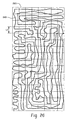
- FIG. 23 shows diagrams of different types of example space-filling, grid dimension, and box-counting curves.
- FIG. 24 shows a diagram of an example of a grid dimension curve.
- FIG. 25 shows a diagram of an example of a grid dimension curve located in a first grid.
- FIG. 26 shows a diagram of an example of a grid dimension curve located in a second grid.
- FIG. 27 shows a diagram of an example of a grid dimension curve located in a third grid.
- FIG. 28 shows a diagram of an example of a box counting curve located in a first curve.
- FIG. 29 shows a diagram of an example of a box counting curve located in a second grid.
- FIG. 30 shows a cross-sectional view of an example package with a semi-conductor die attached to the substrate of the package, and that is covered with a layer of conductive material.
- FIG. 31 shows a cross-sectional view of an example package with a semi-conductor die attached to the substrate of the package with a second substrate placed above the semi-conductor die.
- FIG. 32 shows a cross-sectional view of an example package having a first substrate and a second substrate that is placed above the first substrate of the package, and a semi-conductor die is attached by solder balls underneath the second substrate of the package.
- FIG. 33 shows a cross-sectional view of an example package having a first substrate and a second substrate that is placed above the first substrate of the package, and a semi-conductor die is attached by wire bonds underneath the second substrate of the package.
- FIG. 1 is a schematic view of an antenna 12 in an example integrated circuit (IC) package 11 .
- the IC package 11 includes, among other parts, an antenna 12 including a feeding point 13 and pads or pins 14 .
- No pads or pins 14 which may conduct a signal or be connected to a power or ground plane are located in the antenna 12 projection.
- Antenna projection means the lower or upper projection of the antenna, the lower projection being what is normally understood by the expression underneath the antenna. This location of the pads or pins outside the upper or lower projection (footprint) of the antenna reduces the interaction between the pads and the antenna, preventing a decrease in performance of the antenna.
- the antenna is preferably in the form of a space-filling curve, but other kinds of antennas may also be used.
- the antenna 12 may be included on the same layer or different layers of the IC package as the pads, pins or other components.
- some signal pads could be present in the antenna projection, preferably close to the feeding point 13 .
- the antenna feed point 13 could be accessible through at least a pad or pin of the IC package 11 , and may also be present in the antenna projection without a significant loss in the antenna 12 performance.
- Fixation pads could be present in the example IC package 11 in order to attach the IC package 11 to the PCB.
- these pads When the only function accomplished by these pads is mechanical and no signal or power supply is transmitted by them and no ground is connected to the pins or pads, their effect on the antenna performance is negligible and therefore they may be present in the antenna projection. This arrangement is advantageous in some cases due to the overall reduction on the package or chip size.
- FIG. 2 One example of an advantageous arrangement of an antenna 22 with respect to the pads 14 on a IC package 11 is shown in FIG. 2 .
- the antenna 22 in this example is in the shape of an L-shaped Hilbert space-filling curve. It is located on at least a part of the perimeter of the IC package 11 and the pads 14 are located outside the antenna projection. In other examples, other kinds of antennas may also be used.
- fixation pads 14 could be present in the projection of the antenna. If it is necessary to include electrically conducting pads or other conducting components in the antenna projection, then these should be located as close to the antenna feedpoint 13 as possible. This will minimize the interference with the antenna.
- the functionality or I/O assignment of the pads or pins 14 might be of importance when considering the interaction of the pads or pins 14 with either of the antennas discussed above 12 , 22 .
- the different pad or pin functionalities are powering and grounding, radio frequency functionalities, analog signals, digital buses, and other digital signals, such as signals used for the configuration of the IC.
- the influence of the pins or pads is smaller when close to the antenna feedpoint 13 .
- the pins or pads 14 should thus be located as far away as possible from the end of the antennas 12 , 22 , because the antennas 12 , 22 are most sensitive at the end.
- FIG. 3 shows an example IC package 11 where pins or pads 14 for grounding, powering, and transmitting signals are located at a distance from the antenna projection, and represent around forty percent of the overall surface of the IC package. This percentage could be increased or decreased depending on the particular design constraints.
- ground pins in the projection of either of the antennas 12 , 22 it is advantageous to have the ground pins or pads at a distance from the feeding point 13 that is not larger than one-fifth of the side of the IC package or one-sixtieth of the wavelength in the free space at the operating frequency of the antennas 12 , 22 .
- the digital data pins in the projection of the antennas 12 , 22 it is advantageous to have them at a distance from the feeding point 13 that is not greater than half of the side of the IC package 11 for a package having a side that is one-twelfth of the free-space wavelength of the antenna operating frequency. This would allow the detuning of the antennas 12 , 22 to be kept within a ten percent range.
- ground pins or pads are located at a distance from the feeding point 13 that is not larger than one-half of the side of the IC package or one-twenty-fourth of the wavelength in the free space at the operating frequency of the antennas.
- Signal pads and tracks have a loading effect on the antennas 12 , 22 which leads to a change in the antenna input impedance and resonance frequency. This effect is more severe when pads and tracks are close to the end of the antennas 12 , 22 .
- FIG. 4 shows an example IC package 11 where no tracks cross the projection of the antenna 12 .
- the tracks 41 are at least 1 mm away from the projection of the antenna 12 in a ten-by-ten mm IC package for a Bluetooth Radio IC that operates at 2.4 GHz. Should it be necessary to cross the projection of the antenna 12 , this crossing should preferably be no further than five mm away from the antenna feedpoint 13 in a 10-by-10 mm package for a Bluetooth Radio IC package. The position of the feedpoint 13 could be in or out of the projection of the antenna 12 . Due to the scaling properties of Maxwell's equations, the same features are to be scaled proportionally in packages for other applications working at other wavelengths. For example, in the case of an application running at 1.2 GHz (twice the wavelength for Bluetooth) such signal tracks would preferably cross the antenna footprint at a distance no larger than 10 mm instead of 5 mm.
- the placement of the tracks 14 and the routing of the signals may also affect antenna 12 performance.
- Digital lines filtering could be effective to minimize radio frequency noise. In some examples, this filtering is implemented by any conventional means, for example radio frequency chokes.
- Another option to prevent coupling is to include digital tracks that are mismatched at RF frequencies. Because tracks cannot propagate the radio frequency signals, less power is coupled (hence more isolation is obtained) and less power is delivered to the output ports on the board.
- differential lines In general, the use of differential lines is very effective in suppressing noise and interference when the signal is carried by two lines that have the same potential but that have opposite polarity or phase, and the lines are not referred to a common ground from which interfering signals may be coupled.
- ground planes may be included inside the IC package 11 .
- the greater the distance between the antenna 12 and ground plane the smaller the interaction (in particular the reduction of the antenna input impedance referred to 50 ohms), and therefore the better the antenna performance.
- FIGS. 5 to 8 illustrate several configurations chosen to minimize coupling between the antenna 12 and the internal ground plane.
- the antenna 12 is placed parallel to the ground plane 51 .
- the purpose of this arrangement is to maximize the distance between the antenna 12 and ground plane 51 .
- the distance (d) between the antenna 12 and the ground plane 51 should preferably be 2.5 mm.
- an arrangement where no ground plane 51 is close to the end of the antenna is preferable.
- FIG. 5 illustrates this possibility as an example in a ten-by-ten mm package 11 . Due to the scaling properties of Maxwell's equations, the same features are to be scaled proportionally in packages for other applications working at other wavelengths.
- the ground plane is spaced away from the antenna by at least the greater of one-quarter of a side length of the integrated circuit package and one-fiftieth of a free-space operating wavelength of the antenna.
- FIG. 6 shows an example IC package 11 including a large internal ground plane 51 .
- a part of the ground plane 61 is removed to maximize the distance between the end of the antenna 62 and the ground plane 51 .
- the upper left part of the ground plane has a cut-off.
- Other geometries for the inset or cut-off in the ground plane 61 are also possible.
- FIG. 7 may be preferred.
- ground planes 51 , 81 of different types are present on the IC package. These several ground planes 51 , 81 are typically chosen from the following group: radio frequency, analog, or digital. Different ground planes are included for the purpose of reducing noise.
- two different ground planes 51 , 81 are present on the IC package 11 .
- One of them is a radio frequency ground plane 51
- the other is a digital ground plane 81 .
- the radio frequency circuit in this example is connected to the antenna feeding point 13 ; therefore, it is preferable to minimize the track distance between the feeding point 13 and the RF circuit, for example, by locating the RF ground plane 51 in the position shown in FIG. 8 . In this location, the RF ground plane 51 , which is the ground plane that the antenna 22 is referred to, is far from the end of the antenna 62 .
- the ground planes 51 , 81 may be connected by means of an inductor to filter high frequency currents and balance potentials by means of DC currents. This arrangement may be used to connect planes which are outside the IC package 11 with planes that are inside the IC package 11 .
- ground planes may be included that are arranged at different levels.
- exterior ground planes may be present.
- the IC package 11 may be mounted on a PCB, particularly a multilayer PCB.
- One of the layers of a multilevel PCB is normally a ground plane. If this ground plane is within the projection of the antenna its performance could be decreased.
- One possible solution is to use a PCB where a considerable part of the PCB does not include a ground plane.
- this part of the PCB that does not include a ground plane is also referred to as ‘clearance’.
- FIGS. 9 to 17 illustrate examples where a part of the PCB does not contain a ground plane.
- FIGS. 9 to 17 illustrate arrangements where the ground plane clearance is minimized.
- the coupling between the exterior ground plane and the antenna depends, among other factors, on the shape of the antenna.
- FIGS. 9-11 show a IC package 11 that incorporates an antenna 12 having a projection with a rectangular form.
- a part of the ground plane 92 of the PCB 91 could be located in the projection of the IC package 11 on the PCB 91 , but preferably not in the projection of the antenna 12 .
- FIG. 9 shows an embodiment illustrating an advantageous position of a IC package 11 having a rectangular antenna 12 along its left side, with respect to the PCB 91 .
- FIG. 10 shows an example illustrating how the part of the PCB 91 having a ground plane 92 is maximized while keeping the interaction between antenna 12 and ground plane 92 to a minimum.
- the ground plane 92 has two protrusions 101 , 102 .
- Protrusion A 101 falls inside the IC package 11 while protrusion B 102 is beside the IC package 11 .
- the distance between protrusions A 101 and B 102 serves to minimize the interaction between the external ground plane 92 and the antenna 12 .
- FIG. 11 shows an example where the ground plane 111 is arranged so that the surface of the ground plane 111 is maximized while keeping a distance between it and the end of the antenna 112 .
- FIG. 12 shows an example of an IC package containing an L-shaped Hilbert Space-Filling antenna 22 and placed in a PCB 91 with an area of the PCB 91 free from the ground plane 92 .
- a space-filling antenna 22 has been used in the example of FIG. 12 , in other examples, other types of antennas could also be used.
- the position of the IC package 11 containing the antenna 22 in the upper right-hand corner with respect to the PCB 91 is preferred.
- FIG. 13 shows an example where the part of the PCB 91 having a ground plane 92 is maximized while keeping the interaction between the antenna 22 on the IC package 11 and the ground plane 92 to a minimum.
- Protrusion A 131 falls inside the projection of the IC package 11 while protrusion B 132 is located a distance away from the antenna 22 outside the IC package 11 .
- FIG. 14 shows an example where the IC package 11 includes two internal ground planes 131 , 141 : one ground plane 131 that is part of, or coupled to, the PCB ground plane 92 and another ground plane 141 that is independent from the PCB ground plane 92 . Both ground planes 131 , 141 are situated at a distance from the antenna 22 . One of the ground planes can perform the function of an RF ground plane, while the other can function as a digital ground plane.
- FIG. 15 shows an example of an IC package 11 that is positioned in the middle near the top edge with respect to a PCB 91 .
- the IC package 11 contains an antenna 151 disposed in an horizontal position.
- the inner ground plane 152 of the IC package 11 is also part of, or coupled to, the PCB ground plane 92 .
- FIG. 16 shows an example of an IC package 11 where the part of the PCB having a ground plane 92 is maximized while the interaction between the antenna 151 and ground plane 92 is kept to a minimum.
- Protrusion A 131 falls inside the projection of the IC package while protrusion B 132 is located at a distance from the antenna 151 .
- the antenna 151 is located in a horizontal position with respect to the IC package 11 .
- FIG. 17 shows another example of a IC package 11 where the part of the PCB having a ground plane 92 is maximized while the interaction between the antenna 151 and ground plane 92 is kept to a minimum.
- Protrusion A 131 falls inside the projection of the IC package while protrusion B 132 is located at a distance from the antenna 22 .
- This arrangement is advantageous because the clearance on the PCB 91 outside the IC package 11 is minimized, allowing a smaller PCB 91 and more space for other components.
- Another possibility for preventing decreased performance of the antenna 22 is to use a shielding to isolate a certain part or subsystem of the IC package from the antenna 22 .
- This isolated part of the IC package 11 could be, for example, a pad, track, a ground plane, a circuit, or a silicon part which could be a die.
- FIG. 18 shows an example where the part or subsystem 182 of the IC package to be electrically isolated (the entire IC package is not shown to enhance the clarity of FIG. 18 ) is placed between a lower 184 and an upper 181 metallic conductive piece which covers the die projection. Both plates are electrically connected by means of legs 183 .
- the overall shielding structure might be connected to ground in some examples.
- a part of the lower 184 or upper metallic pieces 181 may have a hole in some examples, so that pads would provide an electrical connection through the lower conductive part.
- FIG. 19 shows a see-through view of an example shielding arrangement 191 similar to that of FIG. 18 with one conductive part over the part or subsystem 182 of the IC package to be isolated.
- lateral walls 192 as well as upper 181 and lower parts 184 , surround the isolated part 182 of the IC package.
- Legs 183 are incorporated in the corners of the cage. These legs 183 might serve to connect lateral walls 192 with the upper 181 and lower parts 184 .
- legs 183 serve to connect the shielding structure to ground. This ground could be the ground plane 201 situated in one of the PCB 202 layers, as shown in FIG. 20 .
- FIG. 20 is a sectional view of the shielding arrangement 191 of FIG. 19 located inside the IC package 11 .
- the part or subsystem of the IC package to be isolated 182 is located inside the shielding arrangement 191 .
- the legs 183 are connected to the PCB 202 ground plane 201 .
- FIG. 21 shows an example of an IC package 11 that includes a conductive plate 195 with a central aperture where the part or subsystem 182 of the IC package to be isolated is located.
- Legs 183 in some examples connect the conductive part which serves as a shielding to ground. The shielding would preferably not be placed in the antenna projection.
- FIG. 22 illustrates an example where the part or subsystem 182 of the IC package to be isolated is located in a cavity formed by an overmold 221 .
- the interior wall of the cavity is covered by a metallic paint 222 and this paint 222 is connected to ground 223 .
- FIG. 22 b shows an example where the overmold 221 is physically in contact with the part or subsystem to be isolated 182 and a metallic paint 222 covers the exterior surface of the overmold 221 . This metallic paint 222 is also connected to ground.
- any of the conductive surfaces mentioned above could be replaced by a grid where the distance between the stripes which form the grid is not more than one-tenth of the free space operating wavelength of the antenna.
- These wires could define a shielding arrangement cage such as that shown in FIG. 19 .
- any of the shieldings mentioned above would cover only partially the part or subsystem 182 of the IC package to be isolated.
- FIG. 23 shows examples of space filling curves.
- Space filling curves 2301 through 2314 are examples of space filling curves for antenna designs.
- Space-filling curves fill the surface or volume where they are located in an efficient way while keeping the linear properties of being curves.
- a Space-filling curve is a non-periodic line composed by a number of connected straight segments smaller than a fraction of the operating free-space wave length of the antenna, where the segments are arranged so that none of the adjacent and connected segments form another longer straight segment and none of the segments intersect with each other.
- the fraction of the operating wavelength is one-tenth or smaller.
- a space-filling curve may have one or more non-straight segments smaller than a fraction of the operating free-space wave length of the antenna, where the segments are arranged so that none of the adjacent and connected segments form another longer segment and none of the segments intersect with each other.
- a grid dimension curve is a curve having a grid dimension greater than one according to the below equation.
- FIG. 24 shows an example of a two-dimensional antenna 2401 forming a grid dimension curve with a grid dimension of approximately two.
- FIG. 25 shows the antenna 2401 of FIG. 24 enclosed in a first grid 2501 having thirty-two 32 square cells, each with a length L 1 . The number of cells (N 1 ) in the first grid that enclose at least a portion of the curve are counted.
- FIG. 26 shows the same antenna 2401 enclosed in a second grid 2601 having one hundred twenty-eight (128) square cells, each with a length L 2 .
- the number of cells (N 2 ) in the second grid that enclose at least a portion of the curve are also counted.
- the value of N 1 in the above grid dimension (Dg) equation is thirty-two (i.e., the total number of cells in the first grid 2501 ), and the value of N 2 is one hundred twenty-eight (i.e., the total number of cells in the second grid 2601 ).
- the grid dimension of the antenna 2401 may be calculated as follows:
- the number of square cells may be increased up to a maximum amount.
- the maximum number of cells in a grid is dependant upon the resolution of the curve. As the number of cells approaches the maximum, the grid dimension calculation becomes more accurate. If a grid having more than the maximum number of cells is selected, however, then the accuracy of the grid dimension calculation begins to decrease.
- the maximum number of cells in a grid is one-thousand.
- FIG. 27 shows the same antenna 2401 enclosed in a third grid 2701 with five hundred twelve (512) square cells, each having a length L 3 .
- the length (L 3 ) of the cells in the third grid is one-half the length (L 2 ) of the cells in the second grid, shown in FIG. 26 .
- N for the second grid 2601 is one hundred twenty-eight (128).
- An examination of FIG. 27 reveals that the antenna 2401 is enclosed within only five-hundred nine of the five-hundred twelve cells of the third grid 2701 . Therefore, the value of N for the third grid 2701 is five-hundred nine.
- a more accurate value for the grid dimension (D g ) of the antenna 2401 may be calculated as follows:
- a box counting antenna has a conducting pattern, at least a portion of which includes a curve, and the curve comprises at least five segments. Each of the at least five segments forms an angle with each adjacent segment in the curve, and at least three of the segments are shorter than one-tenth of the longest free-space operating wavelength of the antenna. Each angle between adjacent segments is less than 180°, at least two of the angles between adjacent sections are less than 115°, and at least two of the angles are not equal.
- the curve fits inside a rectangular area, the longest side of the rectangular area being shorter than one-fifth of the longest free-space operating wavelength of the antenna.
- the box-counting dimension is computed in the following way. First, a grid with cells of size L 1 is placed over the geometry, so that the grid completely covers the geometry, and the number of boxes N 1 that include at least a point of the geometry are counted. Second, a grid with boxes of size L 2 (where L 2 is smaller than L 1 ) is also placed over the geometry, so that the grid completely covers the geometry, and the number of boxes N 2 that include at least a point of the geometry are counted again.
- the box-counting dimension D is then computed as:
- the box-counting dimension is computed by placing the first and second grids inside the minimum rectangular area enclosing the curve of the antenna and applying the above algorithm.
- the minimum rectangular area means an area where there is not an entire row or column on the perimeter of the grid that does not contain any piece of the curve.
- some of the examples may include a box-counting dimension larger than 1.17, and in those applications where the required degree of miniaturization is higher, the designs may feature a box-counting dimension ranging from 1.5 up to 2, inclusive. For some embodiments, a curve having a box-counting dimension of about 2 is preferred.
- the box-counting dimension may be necessarily computed with a finer grid.
- the first grid will be taken as a mesh of ten-by-ten equal cells, while the second grid will be taken as a mesh of twenty-by-twenty equal cells, and then D g is computed according to the equation above.
- One way of enhancing the miniaturization capabilities of the antenna is to arrange the several segments of the curve of the antenna pattern in such a way that the curve intersects at least one point of at least fourteen boxes of the first grid with five-by-five boxes or cells enclosing the curve.
- the curve crosses at least one of the boxes twice within the five-by-five grid, that is, the curve includes two non-adjacent portions inside at least one of the cells or boxes of the grid.
- FIG. 28 and FIG. 29 An example of how the box-counting dimension is computed is shown in FIG. 28 and FIG. 29 .
- the curve 2801 crosses more than 14 of the 25 cells in grid 2802 , and also the curve crosses at least one cell twice, that is, at least one cell contains two non-adjacent segments of the curve. In fact, 2801 is an example where such a double crossing occurs in 13 boxes out of the 25 in 2802 .
- FIGS. 31 through 33 present some embodiments of a package comprising a substrate 3000 , a semiconductor die 3001 , and an antenna 3002 .
- These figures show a cross-sectional view of example packages, which are BGA-type for illustration purposes in these examples.
- the example packages also comprise some additional elements to shield the semiconductor die 3001 from the electromagnetic radiation emitted by the antenna 3002 that is included in the package.
- the semiconductor die 3001 is connected to the substrate 3000 of the package by solder balls 3003 .
- the semiconductor die 3001 has been covered with a layer of a conductive material 3004 which is then connected by one or several wire bonds 3005 to a ground plane.
- the ground plane is internal to the package; however, in other examples the ground plane is external to the package, for example, a conductive layer of the PCB on which the package is mounted may function as an external ground plane. In the latter, the wire bond 3005 will be connected to the external ground plane by means of a ball 3006 , pad or pin of the substrate 3000 of the package.
- FIG. 31 discloses another example in which a second substrate 3020 is located above the semiconductor die 3001 .
- the second substrate 3020 includes a conductive layer 3021 that covers the semiconductor die 3001 .
- the second substrate 3020 is connected to the first substrate 3000 by means of solder balls 3022 , which have a mechanical function of acting as spacers and supporting the second substrate 3020 , and an electrical function of connecting the conducting layer 3021 to a ground plane.
- the ground plane will be internal to the package, while in other examples it will be external to the package.
- the substrate 3000 provides electrical continuity between a solder ball 3022 that is internal to the package and a solder ball 3006 , pad or pin outside of the package.
- FIG. 32 presents another example package similar to the example package of FIG. 31 , but in which the semiconductor die 3001 has been flip-chip bonded to the second substrate 3020 .
- the semiconductor die 3001 is connected to the second substrate 3020 by means of solder balls 3040 .
- the area of the substrate 3000 underneath the projection of the second substrate 3020 could be advantageously covered with a conductive layer to protect the semiconductor die 3001 from electromagnetic radiation.
- FIG. 33 Yet another example package is presented in FIG. 33 , in which the semiconductor die 3001 is flip-chip mounted on the second substrate 3020 , as in FIG. 32 . However, in this example the semiconductor die 3001 is connected to the second substrate 3020 by wire bonds 3060 .
- the example IC packages disclosed herein are advantageously used in wireless devices.
- the antenna arrangement and shielding allows the IC package with antenna to be very small, and particularly useful in mobile wireless devices, for example, laptops, PDA's, cellular phones, and other devices.
Abstract
Description
For a more accurate calculation of the grid dimension, the number of square cells may be increased up to a maximum amount. The maximum number of cells in a grid is dependant upon the resolution of the curve. As the number of cells approaches the maximum, the grid dimension calculation becomes more accurate. If a grid having more than the maximum number of cells is selected, however, then the accuracy of the grid dimension calculation begins to decrease. Typically, the maximum number of cells in a grid is one-thousand.
The box-counting dimension is computed by placing the first and second grids inside the minimum rectangular area enclosing the curve of the antenna and applying the above algorithm.
Claims (50)
Priority Applications (1)
| Application Number | Priority Date | Filing Date | Title |
|---|---|---|---|
| US11/572,380 US8330259B2 (en) | 2004-07-23 | 2005-07-22 | Antenna in package with reduced electromagnetic interaction with on chip elements |
Applications Claiming Priority (3)
| Application Number | Priority Date | Filing Date | Title |
|---|---|---|---|
| US59069504P | 2004-07-23 | 2004-07-23 | |
| PCT/EP2005/008032 WO2006008180A1 (en) | 2004-07-23 | 2005-07-22 | Antenna in package with reduced electromagnetic interaction with on chip elements |
| US11/572,380 US8330259B2 (en) | 2004-07-23 | 2005-07-22 | Antenna in package with reduced electromagnetic interaction with on chip elements |
Publications (2)
| Publication Number | Publication Date |
|---|---|
| US20080265038A1 US20080265038A1 (en) | 2008-10-30 |
| US8330259B2 true US8330259B2 (en) | 2012-12-11 |
Family
ID=35033650
Family Applications (2)
| Application Number | Title | Priority Date | Filing Date |
|---|---|---|---|
| US11/572,380 Active 2028-12-04 US8330259B2 (en) | 2004-07-23 | 2005-07-22 | Antenna in package with reduced electromagnetic interaction with on chip elements |
| US13/673,750 Abandoned US20130313692A1 (en) | 2004-07-23 | 2012-11-09 | Antenna in package with reduced electromagnetic interaction with on chip elements |
Family Applications After (1)
| Application Number | Title | Priority Date | Filing Date |
|---|---|---|---|
| US13/673,750 Abandoned US20130313692A1 (en) | 2004-07-23 | 2012-11-09 | Antenna in package with reduced electromagnetic interaction with on chip elements |
Country Status (3)
| Country | Link |
|---|---|
| US (2) | US8330259B2 (en) |
| EP (1) | EP1771919A1 (en) |
| WO (1) | WO2006008180A1 (en) |
Cited By (131)
| Publication number | Priority date | Publication date | Assignee | Title |
|---|---|---|---|---|
| US9160055B2 (en) | 2012-12-12 | 2015-10-13 | Kabushiki Kaisha Toshiba | Wireless device |
| US9178269B2 (en) | 2011-07-13 | 2015-11-03 | Kabushiki Kaisha Toshiba | Wireless apparatus |
| US9184492B2 (en) | 2010-09-24 | 2015-11-10 | Kabushiki Kaisha Toshiba | Radio device |
| US9245866B2 (en) | 2010-01-05 | 2016-01-26 | Kabushiki Kaisha Toshiba | Antenna device and wireless apparatus |
| US9543641B2 (en) | 2011-07-13 | 2017-01-10 | Kabushiki Kaisha Toshiba | Wireless apparatus |
| US9667317B2 (en) | 2015-06-15 | 2017-05-30 | At&T Intellectual Property I, L.P. | Method and apparatus for providing security using network traffic adjustments |
| US9674711B2 (en) | 2013-11-06 | 2017-06-06 | At&T Intellectual Property I, L.P. | Surface-wave communications and methods thereof |
| US9685992B2 (en) | 2014-10-03 | 2017-06-20 | At&T Intellectual Property I, L.P. | Circuit panel network and methods thereof |
| US9705610B2 (en) | 2014-10-21 | 2017-07-11 | At&T Intellectual Property I, L.P. | Transmission device with impairment compensation and methods for use therewith |
| US9705561B2 (en) | 2015-04-24 | 2017-07-11 | At&T Intellectual Property I, L.P. | Directional coupling device and methods for use therewith |
| US9722318B2 (en) | 2015-07-14 | 2017-08-01 | At&T Intellectual Property I, L.P. | Method and apparatus for coupling an antenna to a device |
| US9729197B2 (en) | 2015-10-01 | 2017-08-08 | At&T Intellectual Property I, L.P. | Method and apparatus for communicating network management traffic over a network |
| US9735833B2 (en) | 2015-07-31 | 2017-08-15 | At&T Intellectual Property I, L.P. | Method and apparatus for communications management in a neighborhood network |
| US9742521B2 (en) | 2014-11-20 | 2017-08-22 | At&T Intellectual Property I, L.P. | Transmission device with mode division multiplexing and methods for use therewith |
| US9742462B2 (en) | 2014-12-04 | 2017-08-22 | At&T Intellectual Property I, L.P. | Transmission medium and communication interfaces and methods for use therewith |
| US9749013B2 (en) | 2015-03-17 | 2017-08-29 | At&T Intellectual Property I, L.P. | Method and apparatus for reducing attenuation of electromagnetic waves guided by a transmission medium |
| US9748626B2 (en) | 2015-05-14 | 2017-08-29 | At&T Intellectual Property I, L.P. | Plurality of cables having different cross-sectional shapes which are bundled together to form a transmission medium |
| US9749053B2 (en) | 2015-07-23 | 2017-08-29 | At&T Intellectual Property I, L.P. | Node device, repeater and methods for use therewith |
| US9769020B2 (en) | 2014-10-21 | 2017-09-19 | At&T Intellectual Property I, L.P. | Method and apparatus for responding to events affecting communications in a communication network |
| US9768833B2 (en) | 2014-09-15 | 2017-09-19 | At&T Intellectual Property I, L.P. | Method and apparatus for sensing a condition in a transmission medium of electromagnetic waves |
| US9769128B2 (en) | 2015-09-28 | 2017-09-19 | At&T Intellectual Property I, L.P. | Method and apparatus for encryption of communications over a network |
| US9780834B2 (en) | 2014-10-21 | 2017-10-03 | At&T Intellectual Property I, L.P. | Method and apparatus for transmitting electromagnetic waves |
| US9787412B2 (en) | 2015-06-25 | 2017-10-10 | At&T Intellectual Property I, L.P. | Methods and apparatus for inducing a fundamental wave mode on a transmission medium |
| US9793954B2 (en) | 2015-04-28 | 2017-10-17 | At&T Intellectual Property I, L.P. | Magnetic coupling device and methods for use therewith |
| US9793951B2 (en) | 2015-07-15 | 2017-10-17 | At&T Intellectual Property I, L.P. | Method and apparatus for launching a wave mode that mitigates interference |
| US9793955B2 (en) | 2015-04-24 | 2017-10-17 | At&T Intellectual Property I, Lp | Passive electrical coupling device and methods for use therewith |
| US9800327B2 (en) | 2014-11-20 | 2017-10-24 | At&T Intellectual Property I, L.P. | Apparatus for controlling operations of a communication device and methods thereof |
| US9820146B2 (en) | 2015-06-12 | 2017-11-14 | At&T Intellectual Property I, L.P. | Method and apparatus for authentication and identity management of communicating devices |
| US9838078B2 (en) | 2015-07-31 | 2017-12-05 | At&T Intellectual Property I, L.P. | Method and apparatus for exchanging communication signals |
| US9838896B1 (en) | 2016-12-09 | 2017-12-05 | At&T Intellectual Property I, L.P. | Method and apparatus for assessing network coverage |
| US20170358862A1 (en) * | 2002-11-07 | 2017-12-14 | Fractus, S.A. | Integrated Circuit Package Including Miniature Antenna |
| US9847850B2 (en) | 2014-10-14 | 2017-12-19 | At&T Intellectual Property I, L.P. | Method and apparatus for adjusting a mode of communication in a communication network |
| US9847566B2 (en) | 2015-07-14 | 2017-12-19 | At&T Intellectual Property I, L.P. | Method and apparatus for adjusting a field of a signal to mitigate interference |
| US9853342B2 (en) | 2015-07-14 | 2017-12-26 | At&T Intellectual Property I, L.P. | Dielectric transmission medium connector and methods for use therewith |
| US9860075B1 (en) | 2016-08-26 | 2018-01-02 | At&T Intellectual Property I, L.P. | Method and communication node for broadband distribution |
| US9865911B2 (en) | 2015-06-25 | 2018-01-09 | At&T Intellectual Property I, L.P. | Waveguide system for slot radiating first electromagnetic waves that are combined into a non-fundamental wave mode second electromagnetic wave on a transmission medium |
| US9866309B2 (en) | 2015-06-03 | 2018-01-09 | At&T Intellectual Property I, Lp | Host node device and methods for use therewith |
| US9871283B2 (en) | 2015-07-23 | 2018-01-16 | At&T Intellectual Property I, Lp | Transmission medium having a dielectric core comprised of plural members connected by a ball and socket configuration |
| US9871282B2 (en) | 2015-05-14 | 2018-01-16 | At&T Intellectual Property I, L.P. | At least one transmission medium having a dielectric surface that is covered at least in part by a second dielectric |
| US9871558B2 (en) | 2014-10-21 | 2018-01-16 | At&T Intellectual Property I, L.P. | Guided-wave transmission device and methods for use therewith |
| US9876571B2 (en) | 2015-02-20 | 2018-01-23 | At&T Intellectual Property I, Lp | Guided-wave transmission device with non-fundamental mode propagation and methods for use therewith |
| US9876264B2 (en) | 2015-10-02 | 2018-01-23 | At&T Intellectual Property I, Lp | Communication system, guided wave switch and methods for use therewith |
| US9876605B1 (en) | 2016-10-21 | 2018-01-23 | At&T Intellectual Property I, L.P. | Launcher and coupling system to support desired guided wave mode |
| US9882257B2 (en) | 2015-07-14 | 2018-01-30 | At&T Intellectual Property I, L.P. | Method and apparatus for launching a wave mode that mitigates interference |
| US9887447B2 (en) | 2015-05-14 | 2018-02-06 | At&T Intellectual Property I, L.P. | Transmission medium having multiple cores and methods for use therewith |
| US9893795B1 (en) | 2016-12-07 | 2018-02-13 | At&T Intellectual Property I, Lp | Method and repeater for broadband distribution |
| US9906269B2 (en) | 2014-09-17 | 2018-02-27 | At&T Intellectual Property I, L.P. | Monitoring and mitigating conditions in a communication network |
| US9904535B2 (en) | 2015-09-14 | 2018-02-27 | At&T Intellectual Property I, L.P. | Method and apparatus for distributing software |
| US9912382B2 (en) | 2015-06-03 | 2018-03-06 | At&T Intellectual Property I, Lp | Network termination and methods for use therewith |
| US9912033B2 (en) | 2014-10-21 | 2018-03-06 | At&T Intellectual Property I, Lp | Guided wave coupler, coupling module and methods for use therewith |
| US9912027B2 (en) | 2015-07-23 | 2018-03-06 | At&T Intellectual Property I, L.P. | Method and apparatus for exchanging communication signals |
| US9911020B1 (en) | 2016-12-08 | 2018-03-06 | At&T Intellectual Property I, L.P. | Method and apparatus for tracking via a radio frequency identification device |
| US9913139B2 (en) | 2015-06-09 | 2018-03-06 | At&T Intellectual Property I, L.P. | Signal fingerprinting for authentication of communicating devices |
| US9917341B2 (en) | 2015-05-27 | 2018-03-13 | At&T Intellectual Property I, L.P. | Apparatus and method for launching electromagnetic waves and for modifying radial dimensions of the propagating electromagnetic waves |
| US9927517B1 (en) | 2016-12-06 | 2018-03-27 | At&T Intellectual Property I, L.P. | Apparatus and methods for sensing rainfall |
| US9929755B2 (en) | 2015-07-14 | 2018-03-27 | At&T Intellectual Property I, L.P. | Method and apparatus for coupling an antenna to a device |
| US9948333B2 (en) | 2015-07-23 | 2018-04-17 | At&T Intellectual Property I, L.P. | Method and apparatus for wireless communications to mitigate interference |
| US9954287B2 (en) | 2014-11-20 | 2018-04-24 | At&T Intellectual Property I, L.P. | Apparatus for converting wireless signals and electromagnetic waves and methods thereof |
| US9954286B2 (en) | 2014-10-21 | 2018-04-24 | At&T Intellectual Property I, L.P. | Guided-wave transmission device with non-fundamental mode propagation and methods for use therewith |
| US9967173B2 (en) | 2015-07-31 | 2018-05-08 | At&T Intellectual Property I, L.P. | Method and apparatus for authentication and identity management of communicating devices |
| US9973416B2 (en) | 2014-10-02 | 2018-05-15 | At&T Intellectual Property I, L.P. | Method and apparatus that provides fault tolerance in a communication network |
| US9973940B1 (en) | 2017-02-27 | 2018-05-15 | At&T Intellectual Property I, L.P. | Apparatus and methods for dynamic impedance matching of a guided wave launcher |
| US9991580B2 (en) | 2016-10-21 | 2018-06-05 | At&T Intellectual Property I, L.P. | Launcher and coupling system for guided wave mode cancellation |
| US9998870B1 (en) | 2016-12-08 | 2018-06-12 | At&T Intellectual Property I, L.P. | Method and apparatus for proximity sensing |
| US9999038B2 (en) | 2013-05-31 | 2018-06-12 | At&T Intellectual Property I, L.P. | Remote distributed antenna system |
| US9997819B2 (en) | 2015-06-09 | 2018-06-12 | At&T Intellectual Property I, L.P. | Transmission medium and method for facilitating propagation of electromagnetic waves via a core |
| US10009067B2 (en) | 2014-12-04 | 2018-06-26 | At&T Intellectual Property I, L.P. | Method and apparatus for configuring a communication interface |
| US10020844B2 (en) | 2016-12-06 | 2018-07-10 | T&T Intellectual Property I, L.P. | Method and apparatus for broadcast communication via guided waves |
| US10027397B2 (en) | 2016-12-07 | 2018-07-17 | At&T Intellectual Property I, L.P. | Distributed antenna system and methods for use therewith |
| US10044409B2 (en) | 2015-07-14 | 2018-08-07 | At&T Intellectual Property I, L.P. | Transmission medium and methods for use therewith |
| US10051630B2 (en) | 2013-05-31 | 2018-08-14 | At&T Intellectual Property I, L.P. | Remote distributed antenna system |
| US10069535B2 (en) | 2016-12-08 | 2018-09-04 | At&T Intellectual Property I, L.P. | Apparatus and methods for launching electromagnetic waves having a certain electric field structure |
| US10069185B2 (en) | 2015-06-25 | 2018-09-04 | At&T Intellectual Property I, L.P. | Methods and apparatus for inducing a non-fundamental wave mode on a transmission medium |
| US10090594B2 (en) | 2016-11-23 | 2018-10-02 | At&T Intellectual Property I, L.P. | Antenna system having structural configurations for assembly |
| US10090606B2 (en) | 2015-07-15 | 2018-10-02 | At&T Intellectual Property I, L.P. | Antenna system with dielectric array and methods for use therewith |
| US20180285706A1 (en) * | 2015-10-06 | 2018-10-04 | Thin Film Electronics Asa | Electronic Device Having an Antenna, Metal Trace(s) and/or Inductor With a Printed Adhesion Promoter Thereon, and Methods of Making and Using the Same |
| US10103422B2 (en) | 2016-12-08 | 2018-10-16 | At&T Intellectual Property I, L.P. | Method and apparatus for mounting network devices |
| US20180332151A1 (en) * | 2015-12-22 | 2018-11-15 | Intel Corporation | Microelectronic devices designed with integrated antennas on a substrate |
| US10135145B2 (en) | 2016-12-06 | 2018-11-20 | At&T Intellectual Property I, L.P. | Apparatus and methods for generating an electromagnetic wave along a transmission medium |
| US10135147B2 (en) | 2016-10-18 | 2018-11-20 | At&T Intellectual Property I, L.P. | Apparatus and methods for launching guided waves via an antenna |
| US10135146B2 (en) | 2016-10-18 | 2018-11-20 | At&T Intellectual Property I, L.P. | Apparatus and methods for launching guided waves via circuits |
| US10139820B2 (en) | 2016-12-07 | 2018-11-27 | At&T Intellectual Property I, L.P. | Method and apparatus for deploying equipment of a communication system |
| US10148016B2 (en) | 2015-07-14 | 2018-12-04 | At&T Intellectual Property I, L.P. | Apparatus and methods for communicating utilizing an antenna array |
| US10168695B2 (en) | 2016-12-07 | 2019-01-01 | At&T Intellectual Property I, L.P. | Method and apparatus for controlling an unmanned aircraft |
| US10178445B2 (en) | 2016-11-23 | 2019-01-08 | At&T Intellectual Property I, L.P. | Methods, devices, and systems for load balancing between a plurality of waveguides |
| US10205655B2 (en) | 2015-07-14 | 2019-02-12 | At&T Intellectual Property I, L.P. | Apparatus and methods for communicating utilizing an antenna array and multiple communication paths |
| US10225025B2 (en) | 2016-11-03 | 2019-03-05 | At&T Intellectual Property I, L.P. | Method and apparatus for detecting a fault in a communication system |
| US10224634B2 (en) | 2016-11-03 | 2019-03-05 | At&T Intellectual Property I, L.P. | Methods and apparatus for adjusting an operational characteristic of an antenna |
| US10243270B2 (en) | 2016-12-07 | 2019-03-26 | At&T Intellectual Property I, L.P. | Beam adaptive multi-feed dielectric antenna system and methods for use therewith |
| US10243784B2 (en) | 2014-11-20 | 2019-03-26 | At&T Intellectual Property I, L.P. | System for generating topology information and methods thereof |
| US10264586B2 (en) | 2016-12-09 | 2019-04-16 | At&T Mobility Ii Llc | Cloud-based packet controller and methods for use therewith |
| US10291334B2 (en) | 2016-11-03 | 2019-05-14 | At&T Intellectual Property I, L.P. | System for detecting a fault in a communication system |
| US10298293B2 (en) | 2017-03-13 | 2019-05-21 | At&T Intellectual Property I, L.P. | Apparatus of communication utilizing wireless network devices |
| US10305190B2 (en) | 2016-12-01 | 2019-05-28 | At&T Intellectual Property I, L.P. | Reflecting dielectric antenna system and methods for use therewith |
| US10312567B2 (en) | 2016-10-26 | 2019-06-04 | At&T Intellectual Property I, L.P. | Launcher with planar strip antenna and methods for use therewith |
| US10326494B2 (en) | 2016-12-06 | 2019-06-18 | At&T Intellectual Property I, L.P. | Apparatus for measurement de-embedding and methods for use therewith |
| US10326689B2 (en) | 2016-12-08 | 2019-06-18 | At&T Intellectual Property I, L.P. | Method and system for providing alternative communication paths |
| US10340603B2 (en) | 2016-11-23 | 2019-07-02 | At&T Intellectual Property I, L.P. | Antenna system having shielded structural configurations for assembly |
| US10340591B2 (en) | 2014-04-29 | 2019-07-02 | Hewlett-Packard Development Company, L.P. | Antenna with bridged ground planes |
| US10340573B2 (en) | 2016-10-26 | 2019-07-02 | At&T Intellectual Property I, L.P. | Launcher with cylindrical coupling device and methods for use therewith |
| US10340983B2 (en) | 2016-12-09 | 2019-07-02 | At&T Intellectual Property I, L.P. | Method and apparatus for surveying remote sites via guided wave communications |
| US10340600B2 (en) | 2016-10-18 | 2019-07-02 | At&T Intellectual Property I, L.P. | Apparatus and methods for launching guided waves via plural waveguide systems |
| US10340601B2 (en) | 2016-11-23 | 2019-07-02 | At&T Intellectual Property I, L.P. | Multi-antenna system and methods for use therewith |
| US10355367B2 (en) | 2015-10-16 | 2019-07-16 | At&T Intellectual Property I, L.P. | Antenna structure for exchanging wireless signals |
| US10359749B2 (en) | 2016-12-07 | 2019-07-23 | At&T Intellectual Property I, L.P. | Method and apparatus for utilities management via guided wave communication |
| US10361489B2 (en) | 2016-12-01 | 2019-07-23 | At&T Intellectual Property I, L.P. | Dielectric dish antenna system and methods for use therewith |
| US10374316B2 (en) | 2016-10-21 | 2019-08-06 | At&T Intellectual Property I, L.P. | System and dielectric antenna with non-uniform dielectric |
| US10382976B2 (en) | 2016-12-06 | 2019-08-13 | At&T Intellectual Property I, L.P. | Method and apparatus for managing wireless communications based on communication paths and network device positions |
| US10389029B2 (en) | 2016-12-07 | 2019-08-20 | At&T Intellectual Property I, L.P. | Multi-feed dielectric antenna system with core selection and methods for use therewith |
| US10389037B2 (en) | 2016-12-08 | 2019-08-20 | At&T Intellectual Property I, L.P. | Apparatus and methods for selecting sections of an antenna array and use therewith |
| US10411356B2 (en) | 2016-12-08 | 2019-09-10 | At&T Intellectual Property I, L.P. | Apparatus and methods for selectively targeting communication devices with an antenna array |
| US10439675B2 (en) | 2016-12-06 | 2019-10-08 | At&T Intellectual Property I, L.P. | Method and apparatus for repeating guided wave communication signals |
| US10446936B2 (en) | 2016-12-07 | 2019-10-15 | At&T Intellectual Property I, L.P. | Multi-feed dielectric antenna system and methods for use therewith |
| US10498044B2 (en) | 2016-11-03 | 2019-12-03 | At&T Intellectual Property I, L.P. | Apparatus for configuring a surface of an antenna |
| US10530505B2 (en) | 2016-12-08 | 2020-01-07 | At&T Intellectual Property I, L.P. | Apparatus and methods for launching electromagnetic waves along a transmission medium |
| US10535928B2 (en) | 2016-11-23 | 2020-01-14 | At&T Intellectual Property I, L.P. | Antenna system and methods for use therewith |
| US10547348B2 (en) | 2016-12-07 | 2020-01-28 | At&T Intellectual Property I, L.P. | Method and apparatus for switching transmission mediums in a communication system |
| US10601494B2 (en) | 2016-12-08 | 2020-03-24 | At&T Intellectual Property I, L.P. | Dual-band communication device and method for use therewith |
| US10637149B2 (en) | 2016-12-06 | 2020-04-28 | At&T Intellectual Property I, L.P. | Injection molded dielectric antenna and methods for use therewith |
| US10650940B2 (en) | 2015-05-15 | 2020-05-12 | At&T Intellectual Property I, L.P. | Transmission medium having a conductive material and methods for use therewith |
| US10694379B2 (en) | 2016-12-06 | 2020-06-23 | At&T Intellectual Property I, L.P. | Waveguide system with device-based authentication and methods for use therewith |
| US10727599B2 (en) | 2016-12-06 | 2020-07-28 | At&T Intellectual Property I, L.P. | Launcher with slot antenna and methods for use therewith |
| US10755542B2 (en) | 2016-12-06 | 2020-08-25 | At&T Intellectual Property I, L.P. | Method and apparatus for surveillance via guided wave communication |
| US10777873B2 (en) | 2016-12-08 | 2020-09-15 | At&T Intellectual Property I, L.P. | Method and apparatus for mounting network devices |
| US10797781B2 (en) | 2015-06-03 | 2020-10-06 | At&T Intellectual Property I, L.P. | Client node device and methods for use therewith |
| US10811767B2 (en) | 2016-10-21 | 2020-10-20 | At&T Intellectual Property I, L.P. | System and dielectric antenna with convex dielectric radome |
| US10819035B2 (en) | 2016-12-06 | 2020-10-27 | At&T Intellectual Property I, L.P. | Launcher with helical antenna and methods for use therewith |
| US10916969B2 (en) | 2016-12-08 | 2021-02-09 | At&T Intellectual Property I, L.P. | Method and apparatus for providing power using an inductive coupling |
| US10923818B2 (en) | 2017-09-21 | 2021-02-16 | City University Of Hong Kong | Dual-fed dual-frequency hollow dielectric antenna |
| US10938108B2 (en) | 2016-12-08 | 2021-03-02 | At&T Intellectual Property I, L.P. | Frequency selective multi-feed dielectric antenna system and methods for use therewith |
| US11901623B2 (en) | 2020-08-18 | 2024-02-13 | Georgia Tech Research Corporation | RF systems on antenna and method of fabrication |
Families Citing this family (16)
| Publication number | Priority date | Publication date | Assignee | Title |
|---|---|---|---|---|
| US8196829B2 (en) | 2006-06-23 | 2012-06-12 | Fractus, S.A. | Chip module, sim card, wireless device and wireless communication method |
| US8738103B2 (en) | 2006-07-18 | 2014-05-27 | Fractus, S.A. | Multiple-body-configuration multimedia and smartphone multifunction wireless devices |
| WO2008111914A1 (en) | 2007-03-09 | 2008-09-18 | Nanyang Technological University | An integrated circuit structure and a method of forming the same |
| US8649820B2 (en) | 2011-11-07 | 2014-02-11 | Blackberry Limited | Universal integrated circuit card apparatus and related methods |
| USD703208S1 (en) * | 2012-04-13 | 2014-04-22 | Blackberry Limited | UICC apparatus |
| US8936199B2 (en) | 2012-04-13 | 2015-01-20 | Blackberry Limited | UICC apparatus and related methods |
| USD701864S1 (en) * | 2012-04-23 | 2014-04-01 | Blackberry Limited | UICC apparatus |
| US9225388B2 (en) | 2012-07-03 | 2015-12-29 | Intel Corporation | Transmitting magnetic field through metal chassis using fractal surfaces |
| US9196958B2 (en) | 2012-07-26 | 2015-11-24 | Apple Inc. | Antenna structures and shield layers on packaged wireless circuits |
| US10784208B2 (en) * | 2015-09-10 | 2020-09-22 | Advanced Semiconductor Engineering, Inc. | Semiconductor package device and method of manufacturing the same |
| MY191810A (en) * | 2016-12-21 | 2022-07-16 | Intel Corp | Slot antenna on a printed circuit board (pcb) |
| US11201119B2 (en) | 2018-06-06 | 2021-12-14 | At&S Austria Technologie & Systemtechnik Aktiengesellschaft | RF functionality and electromagnetic radiation shielding in a component carrier |
| US11664872B2 (en) | 2019-01-31 | 2023-05-30 | Spreadtrum Communications (Shanghai) Co., Ltd. | Beam detection method and device, beam adjusting method and device, antenna module selection method and device, and computer readable storage media |
| CN111294093B (en) * | 2019-01-31 | 2022-03-22 | 展讯通信(上海)有限公司 | AiP structure-based beam detection method and device and computer-readable storage medium |
| CN110828065B (en) * | 2019-06-27 | 2021-12-17 | 北京品驰医疗设备有限公司 | Grooving pattern generation method for suppressing eddy current effect and charging medium manufacturing method |
| EP4241383A1 (en) * | 2020-11-03 | 2023-09-13 | Intel Corporation | Distributed radiohead system |
Citations (117)
| Publication number | Priority date | Publication date | Assignee | Title |
|---|---|---|---|---|
| US4232277A (en) | 1979-03-09 | 1980-11-04 | The United States Of America As Represented By The Secretary Of The Army | Microwave oscillator for microwave integrated circuit applications |
| JPS62262502A (en) | 1986-05-09 | 1987-11-14 | Yuniden Kk | Antenna for radio communication equipment |
| US4751513A (en) | 1986-05-02 | 1988-06-14 | Rca Corporation | Light controlled antennas |
| US4843468A (en) | 1986-07-14 | 1989-06-27 | British Broadcasting Corporation | Scanning techniques using hierarchical set of curves |
| JPH01311605A (en) | 1988-06-08 | 1989-12-15 | Nec Corp | Microwave integrated circuit |
| EP0523564A1 (en) | 1991-07-15 | 1993-01-20 | Sumitomo Electric Industries, Ltd. | An oscillating circuit with a ring shaped resonator of superconducting material coupled thereto |
| US5363114A (en) | 1990-01-29 | 1994-11-08 | Shoemaker Kevin O | Planar serpentine antennas |
| US5386214A (en) | 1989-02-14 | 1995-01-31 | Fujitsu Limited | Electronic circuit device |
| JPH0852968A (en) | 1994-02-14 | 1996-02-27 | Gemplus Card Internatl Sa | Non-contact card and its production |
| DE19500925A1 (en) | 1995-01-16 | 1996-07-18 | Orga Kartensysteme Gmbh | Integrated circuit (I.C) card or "chip" card |
| US5569879A (en) | 1991-02-19 | 1996-10-29 | Gemplus Card International | Integrated circuit micromodule obtained by the continuous assembly of patterned strips |
| WO1997006578A1 (en) | 1995-08-09 | 1997-02-20 | Fractal Antenna Systems, Inc. | Fractal antennas, resonators and loading elements |
| JPH0983240A (en) | 1995-09-12 | 1997-03-28 | Toshiba Corp | Communication module |
| US5621913A (en) | 1992-05-15 | 1997-04-15 | Micron Technology, Inc. | System with chip to chip communication |
| US5621199A (en) | 1995-04-03 | 1997-04-15 | Datalogic, Inc. | RFID reader |
| US5710458A (en) | 1993-12-20 | 1998-01-20 | Kabushiki Kaisha Toshiba | Card like semiconductor device |
| ES2112163A1 (en) | 1995-05-19 | 1998-03-16 | Univ Catalunya Politecnica | Fractal or multi-fractal aerials. |
| EP0902472A2 (en) | 1997-09-15 | 1999-03-17 | Microchip Technology Inc. | Combination inductive coil and integrated circuit semiconductor chip in a single lead frame package and method therefor |
| US5886669A (en) | 1995-05-10 | 1999-03-23 | Casio Computer Co., Ltd. | Antenna for use with a portable radio apparatus |
| US5892661A (en) | 1996-10-31 | 1999-04-06 | Motorola, Inc. | Smartcard and method of making |
| EP0909089A1 (en) | 1997-04-06 | 1999-04-14 | Sony Corporation | Signal processor and signal processing method |
| US5903239A (en) | 1994-08-11 | 1999-05-11 | Matsushita Electric Industrial Co., Ltd. | Micro-patch antenna connected to circuits chips |
| WO1999027608A1 (en) | 1997-11-22 | 1999-06-03 | Nathan Cohen | Cylindrical conformable antenna on a planar substrate |
| WO1999035691A1 (en) | 1998-01-09 | 1999-07-15 | Microchip Technology Incorporated | An integrated circuit (ic) package including accompanying ic chip and coil and a method of production therefor |
| US6011518A (en) | 1996-07-26 | 2000-01-04 | Harness System Technologies Research, Ltd. | Vehicle antenna |
| EP0969375A2 (en) | 1998-06-30 | 2000-01-05 | Sun Microsystems, Inc. | Method for visualizing locality within an address space |
| EP0978729A2 (en) | 1998-08-07 | 2000-02-09 | Hitachi, Ltd. | High-frequency transmitter-receiving apparatus for such an application as vehicle-onboard radar system |
| US6052093A (en) | 1996-12-18 | 2000-04-18 | Savi Technology, Inc. | Small omni-directional, slot antenna |
| WO2000025266A1 (en) | 1998-10-23 | 2000-05-04 | Stmicroelectronics S.A. | Self-adhesive electronic circuit |
| WO2000034916A1 (en) | 1998-12-04 | 2000-06-15 | Gemplus | Contactless electronic module, chip card comprising same, and methods for making same |
| US6087990A (en) | 1999-02-02 | 2000-07-11 | Antenna Plus, Llc | Dual function communication antenna |
| US6107920A (en) | 1998-06-09 | 2000-08-22 | Motorola, Inc. | Radio frequency identification tag having an article integrated antenna |
| US6147655A (en) | 1998-11-05 | 2000-11-14 | Single Chip Systems Corporation | Flat loop antenna in a single plane for use in radio frequency identification tags |
| WO2000077728A1 (en) | 1999-06-15 | 2000-12-21 | Gemplus | Cards and method for making cards having a communication interface with and without contact |
| WO2001005048A1 (en) | 1999-07-14 | 2001-01-18 | Filtronic Lk Oy | Structure of a radio-frequency front end |
| WO2001004957A1 (en) | 1999-07-08 | 2001-01-18 | Gemplus | Contactless electronic module and method for obtaining same |
| WO2001008093A1 (en) | 1999-07-23 | 2001-02-01 | Gemplus | Minicard with integrated circuit and method for obtaining same |
| EP1085597A2 (en) | 1999-09-15 | 2001-03-21 | Lucent Technologies Inc. | Antenna package for a wireless communications device |
| WO2001022528A1 (en) | 1999-09-20 | 2001-03-29 | Fractus, S.A. | Multilevel antennae |
| US6236366B1 (en) | 1996-09-02 | 2001-05-22 | Olympus Optical Co., Ltd. | Hermetically sealed semiconductor module composed of semiconductor integrated circuit and antenna element |
| US6240301B1 (en) | 1998-10-29 | 2001-05-29 | Ericcson Inc. | Diversity antenna in a SIM card package |
| US6239752B1 (en) | 1995-02-28 | 2001-05-29 | Stmicroelectronics, Inc. | Semiconductor chip package that is also an antenna |
| US6263193B1 (en) | 1997-03-28 | 2001-07-17 | Kabushiki Kaisha Toshiba | Microwave transmitter/receiver module |
| WO2001054225A1 (en) | 2000-01-19 | 2001-07-26 | Fractus, S.A. | Space-filling miniature antennas |
| US6268796B1 (en) | 1997-12-12 | 2001-07-31 | Alfred Gnadinger | Radio frequency identification transponder having integrated antenna |
| EP1126522A1 (en) | 2000-02-18 | 2001-08-22 | Alcatel | Packaged integrated circuit with radio frequency antenna |
| US6281848B1 (en) | 1999-06-25 | 2001-08-28 | Murata Manufacturing Co., Ltd. | Antenna device and communication apparatus using the same |
| US6285342B1 (en) | 1998-10-30 | 2001-09-04 | Intermec Ip Corp. | Radio frequency tag with miniaturized resonant antenna |
| EP1130677A2 (en) | 2000-02-29 | 2001-09-05 | Lucent Technologies Inc. | Patch antenna with finite ground plane |
| US6320543B1 (en) | 1999-03-24 | 2001-11-20 | Nec Corporation | Microwave and millimeter wave circuit apparatus |
| US20010046126A1 (en) | 2000-02-18 | 2001-11-29 | Colello Gary M. | Flip-chip RF-ID tag |
| WO2002001495A1 (en) | 2000-06-26 | 2002-01-03 | Gemplus | Hybrid card with ohmic contact and delocalized sinks |
| US20020005433A1 (en) | 1998-01-07 | 2002-01-17 | Hideo Nochi | Non-contact ic card |
| US20020033773A1 (en) | 2000-09-19 | 2002-03-21 | Takayuki Hirabayashi | Antenna Device and radio communication card module having antenna device |
| US6366260B1 (en) | 1998-11-02 | 2002-04-02 | Intermec Ip Corp. | RFID tag employing hollowed monopole antenna |
| WO2002029929A2 (en) | 2000-10-03 | 2002-04-11 | Marconi Corporation Plc | Multi-band wireless communication device |
| US6373447B1 (en) | 1998-12-28 | 2002-04-16 | Kawasaki Steel Corporation | On-chip antenna, and systems utilizing same |
| EP1198027A1 (en) | 2000-10-12 | 2002-04-17 | The Furukawa Electric Co., Ltd. | Small antenna |
| US6388631B1 (en) | 2001-03-19 | 2002-05-14 | Hrl Laboratories Llc | Reconfigurable interleaved phased array antenna |
| US20020058539A1 (en) | 1999-09-13 | 2002-05-16 | Paul A. Underbrink | Directional antenna for hand-held wireless communications device |
| JP2002141726A (en) | 2000-11-02 | 2002-05-17 | Yokowo Co Ltd | Antenna incorporated with electronic component |
| JP2002158529A (en) | 2000-11-20 | 2002-05-31 | Murata Mfg Co Ltd | Surface-mounted antenna structure and communications equipment provided with the same |
| US20020089456A1 (en) | 2001-01-11 | 2002-07-11 | Hiroki Hamada | Chip antenna and method of manufacturing the same |
| US6421013B1 (en) | 1999-10-04 | 2002-07-16 | Amerasia International Technology, Inc. | Tamper-resistant wireless article including an antenna |
| US20020094661A1 (en) | 1999-10-01 | 2002-07-18 | Ziptronix | Three dimensional device intergration method and intergrated device |
| US6424315B1 (en) | 2000-08-02 | 2002-07-23 | Amkor Technology, Inc. | Semiconductor chip having a radio-frequency identification transceiver |
| EP1227540A1 (en) | 2001-01-30 | 2002-07-31 | Alps Electric Co., Ltd. | Partial ground connection of a metal housing for realising certain electrical lenghts for the ground connection of a chip antenna |
| WO2002060004A2 (en) | 2001-01-06 | 2002-08-01 | Telisar Corporation | An integrated antenna system |
| US20020101382A1 (en) | 2001-02-01 | 2002-08-01 | Takayoshi Konishi | Chip antenna and antenna unit including the same |
| JP2002299933A (en) | 2001-04-02 | 2002-10-11 | Murata Mfg Co Ltd | Electrode structure for antenna and communication equipment provided with the same |
| US6465880B1 (en) * | 1997-08-28 | 2002-10-15 | Nippon Telegraph And Telephone Corporation | IC card indicating state of usage and system therefor |
| US6476767B2 (en) | 2000-04-14 | 2002-11-05 | Hitachi Metals, Ltd. | Chip antenna element, antenna apparatus and communications apparatus comprising same |
| WO2002095869A1 (en) | 2001-05-25 | 2002-11-28 | Koninklijke Philips Electronics N.V. | Radio communications device with slot antenna |
| WO2002096166A1 (en) | 2001-05-18 | 2002-11-28 | Corporation For National Research Initiatives | Radio frequency microelectromechanical systems (mems) devices on low-temperature co-fired ceramic (ltcc) substrates |
| US6509825B1 (en) | 1999-09-24 | 2003-01-21 | Microchip Technology Incorporated | Integrated circuit device having a self-biased, single pin radio frequency signal input |
| US6512482B1 (en) | 2001-03-20 | 2003-01-28 | Xilinx, Inc. | Method and apparatus using a semiconductor die integrated antenna structure |
| US6535175B2 (en) | 2000-06-01 | 2003-03-18 | Intermec Ip Corp. | Adjustable length antenna system for RF transponders |
| EP1307017A1 (en) | 2001-10-24 | 2003-05-02 | Siemens Aktiengesellschaft | Method and system for radio data networks access authentication |
| US6563463B1 (en) | 1999-05-24 | 2003-05-13 | Hitachi, Ltd. | Wireless tag, its manufacturing and its layout |
| US20030102544A1 (en) * | 2001-12-03 | 2003-06-05 | Masataka Nishikawa | Semiconductor module and production method therefor and module for IC cards and the like |
| WO2003050913A1 (en) | 2001-12-10 | 2003-06-19 | Fractus, S.A. | Contactless identification device |
| EP1326302A2 (en) | 2001-12-28 | 2003-07-09 | Zarlink Semiconductor (U.S.) Inc. | Integrated circuit fractal antenna in a hearing aid device |
| US6611237B2 (en) | 2000-11-30 | 2003-08-26 | The Regents Of The University Of California | Fluidic self-assembly of active antenna |
| US6646609B2 (en) | 2001-08-07 | 2003-11-11 | Murata Manufacturing Co., Ltd. | Antenna with an integral RF circuit, antenna module incorporating the same, and communication apparatus incorporating the same |
| WO2003096475A1 (en) | 2002-05-09 | 2003-11-20 | Koninklijke Philips Electronics N.V. | Antenna arrangement and module including the arrangement |
| US6657592B2 (en) | 2002-04-26 | 2003-12-02 | Rf Micro Devices, Inc. | Patch antenna |
| US6670921B2 (en) | 2001-07-13 | 2003-12-30 | Hrl Laboratories, Llc | Low-cost HDMI-D packaging technique for integrating an efficient reconfigurable antenna array with RF MEMS switches and a high impedance surface |
| US6674409B2 (en) | 2000-12-05 | 2004-01-06 | Microtune (San Diego), Inc. | Balanced antenna structure for bluetooth 2.4 GHz physical region semiconductor integrated circuit |
| US20040014428A1 (en) | 2002-07-16 | 2004-01-22 | Franca-Neto Luiz M. | RF/microwave system with a system on a chip package or the like |
| US6697021B2 (en) | 2002-01-14 | 2004-02-24 | Microtune (San Diego), Inc. | Double F antenna |
| WO2004019261A2 (en) | 2002-08-26 | 2004-03-04 | Dai Nippon Printing Co., Ltd. | Sim, sim holder, ic module, ic card and ic card holder |
| WO2004021271A1 (en) | 2002-08-30 | 2004-03-11 | Stmicroelectronics Sa | Antenna communication method for a chip card and associated device |
| WO2004025778A1 (en) | 2002-09-10 | 2004-03-25 | Fractus, S.A. | Coupled multiband antennas |
| EP1403960A1 (en) | 2001-04-12 | 2004-03-31 | NEC Corporation | Mobile radio-utilizing device |
| JP2004104344A (en) | 2002-09-06 | 2004-04-02 | Sharp Corp | Dipole antenna, tag using the same, and mobile unit identification system |
| US6716103B1 (en) | 1999-10-07 | 2004-04-06 | Nintendo Co., Ltd. | Portable game machine |
| US6717494B2 (en) | 2001-06-21 | 2004-04-06 | Nec Toppan Circuit Solutions, Inc. | Printed-circuit board, coaxial cable, and electronic device |
| WO2004042868A1 (en) | 2002-11-07 | 2004-05-21 | Fractus, S.A. | Integrated circuit package including miniature antenna |
| US6744411B1 (en) | 2002-12-23 | 2004-06-01 | The Boeing Company | Electronically scanned antenna system, an electrically scanned antenna and an associated method of forming the same |
| FR2848025A1 (en) | 2002-11-28 | 2004-06-04 | Gemplus Card Int | Protection of an electronic component by a conducting layer with random contact for integrity verification, comprises insulating grid forming micro-channels for access to micro-sensors |
| US6745945B1 (en) | 1999-04-29 | 2004-06-08 | Schlumberger Systemes | Method for making contactless cards by lamination and contactless card obtained by said method |
| US20040119644A1 (en) | 2000-10-26 | 2004-06-24 | Carles Puente-Baliarda | Antenna system for a motor vehicle |
| US20040129785A1 (en) | 2001-11-06 | 2004-07-08 | Luu Daniel V. H. | Contactless SIM card carrier with detachable antenna and carrier therefore |
| US20040129786A1 (en) | 2001-02-02 | 2004-07-08 | Yves Reignoux | Portable object with chip and antenna |
| US20040137971A1 (en) * | 2002-11-06 | 2004-07-15 | Hideaki Shoji | Wireless communication apparatus |
| US20040222930A1 (en) | 2003-05-07 | 2004-11-11 | Huei-Hsin Sun | Wrist antenna |
| US6819293B2 (en) | 2001-02-13 | 2004-11-16 | Koninklijke Philips Electronics N.V. | Patch antenna with switchable reactive components for multiple frequency use in mobile communications |
| US20040246187A1 (en) | 2003-06-05 | 2004-12-09 | Tsutomu Hara | Printed circuit board and wireless communication apparatus |
| US20050238149A1 (en) | 2004-04-24 | 2005-10-27 | De Leon Hilary L | Cellular phone-based automatic payment system |
| WO2005109330A1 (en) | 2004-05-06 | 2005-11-17 | Fractus, S.A. | Radio-frequency system in package including antenna |
| US6998709B2 (en) * | 2003-11-05 | 2006-02-14 | Broadcom Corp. | RFIC die-package configuration |
| US20060076658A1 (en) | 2004-10-13 | 2006-04-13 | Advanced Semiconductor Engineering, Inc. | Semiconductor package structure with microstrip antennan |
| US20060141958A1 (en) | 2004-12-29 | 2006-06-29 | Brosnan Michael J | Non-resonant antennas embedded in wireless peripherals |
| US20060170610A1 (en) | 2005-01-28 | 2006-08-03 | Tenatronics Limited | Antenna system for remote control automotive application |
| WO2006120250A2 (en) | 2005-05-13 | 2006-11-16 | Fractus, S.A. | Antenna diversity system and slot antenna component |
| WO2007028448A1 (en) | 2005-07-21 | 2007-03-15 | Fractus, S.A. | Handheld device with two antennas, and method of enhancing the isolation between the antennas |
| US7586414B2 (en) | 2004-02-27 | 2009-09-08 | Fujitsu Limited | Radio tag |
-
2005
- 2005-07-22 WO PCT/EP2005/008032 patent/WO2006008180A1/en active Application Filing
- 2005-07-22 EP EP05761383A patent/EP1771919A1/en not_active Withdrawn
- 2005-07-22 US US11/572,380 patent/US8330259B2/en active Active
-
2012
- 2012-11-09 US US13/673,750 patent/US20130313692A1/en not_active Abandoned
Patent Citations (124)
| Publication number | Priority date | Publication date | Assignee | Title |
|---|---|---|---|---|
| US4232277A (en) | 1979-03-09 | 1980-11-04 | The United States Of America As Represented By The Secretary Of The Army | Microwave oscillator for microwave integrated circuit applications |
| US4751513A (en) | 1986-05-02 | 1988-06-14 | Rca Corporation | Light controlled antennas |
| JPS62262502A (en) | 1986-05-09 | 1987-11-14 | Yuniden Kk | Antenna for radio communication equipment |
| US4843468A (en) | 1986-07-14 | 1989-06-27 | British Broadcasting Corporation | Scanning techniques using hierarchical set of curves |
| US4843468B1 (en) | 1986-07-14 | 1993-12-21 | British Broadcasting Corporation | Scanning techniques using hierarchial set of curves |
| JPH01311605A (en) | 1988-06-08 | 1989-12-15 | Nec Corp | Microwave integrated circuit |
| US5386214A (en) | 1989-02-14 | 1995-01-31 | Fujitsu Limited | Electronic circuit device |
| US5363114A (en) | 1990-01-29 | 1994-11-08 | Shoemaker Kevin O | Planar serpentine antennas |
| US5569879A (en) | 1991-02-19 | 1996-10-29 | Gemplus Card International | Integrated circuit micromodule obtained by the continuous assembly of patterned strips |
| EP0523564A1 (en) | 1991-07-15 | 1993-01-20 | Sumitomo Electric Industries, Ltd. | An oscillating circuit with a ring shaped resonator of superconducting material coupled thereto |
| US5621913A (en) | 1992-05-15 | 1997-04-15 | Micron Technology, Inc. | System with chip to chip communication |
| US5710458A (en) | 1993-12-20 | 1998-01-20 | Kabushiki Kaisha Toshiba | Card like semiconductor device |
| JPH0852968A (en) | 1994-02-14 | 1996-02-27 | Gemplus Card Internatl Sa | Non-contact card and its production |
| US5903239A (en) | 1994-08-11 | 1999-05-11 | Matsushita Electric Industrial Co., Ltd. | Micro-patch antenna connected to circuits chips |
| DE19500925A1 (en) | 1995-01-16 | 1996-07-18 | Orga Kartensysteme Gmbh | Integrated circuit (I.C) card or "chip" card |
| US6239752B1 (en) | 1995-02-28 | 2001-05-29 | Stmicroelectronics, Inc. | Semiconductor chip package that is also an antenna |
| US5621199A (en) | 1995-04-03 | 1997-04-15 | Datalogic, Inc. | RFID reader |
| US5886669A (en) | 1995-05-10 | 1999-03-23 | Casio Computer Co., Ltd. | Antenna for use with a portable radio apparatus |
| ES2112163A1 (en) | 1995-05-19 | 1998-03-16 | Univ Catalunya Politecnica | Fractal or multi-fractal aerials. |
| WO1997006578A1 (en) | 1995-08-09 | 1997-02-20 | Fractal Antenna Systems, Inc. | Fractal antennas, resonators and loading elements |
| JPH0983240A (en) | 1995-09-12 | 1997-03-28 | Toshiba Corp | Communication module |
| US6011518A (en) | 1996-07-26 | 2000-01-04 | Harness System Technologies Research, Ltd. | Vehicle antenna |
| US6236366B1 (en) | 1996-09-02 | 2001-05-22 | Olympus Optical Co., Ltd. | Hermetically sealed semiconductor module composed of semiconductor integrated circuit and antenna element |
| US5892661A (en) | 1996-10-31 | 1999-04-06 | Motorola, Inc. | Smartcard and method of making |
| US6052093A (en) | 1996-12-18 | 2000-04-18 | Savi Technology, Inc. | Small omni-directional, slot antenna |
| US6263193B1 (en) | 1997-03-28 | 2001-07-17 | Kabushiki Kaisha Toshiba | Microwave transmitter/receiver module |
| EP0909089A1 (en) | 1997-04-06 | 1999-04-14 | Sony Corporation | Signal processor and signal processing method |
| US6465880B1 (en) * | 1997-08-28 | 2002-10-15 | Nippon Telegraph And Telephone Corporation | IC card indicating state of usage and system therefor |
| EP0902472A2 (en) | 1997-09-15 | 1999-03-17 | Microchip Technology Inc. | Combination inductive coil and integrated circuit semiconductor chip in a single lead frame package and method therefor |
| WO1999027608A1 (en) | 1997-11-22 | 1999-06-03 | Nathan Cohen | Cylindrical conformable antenna on a planar substrate |
| US6268796B1 (en) | 1997-12-12 | 2001-07-31 | Alfred Gnadinger | Radio frequency identification transponder having integrated antenna |
| US20020005433A1 (en) | 1998-01-07 | 2002-01-17 | Hideo Nochi | Non-contact ic card |
| WO1999035691A1 (en) | 1998-01-09 | 1999-07-15 | Microchip Technology Incorporated | An integrated circuit (ic) package including accompanying ic chip and coil and a method of production therefor |
| US6107920A (en) | 1998-06-09 | 2000-08-22 | Motorola, Inc. | Radio frequency identification tag having an article integrated antenna |
| EP0969375A2 (en) | 1998-06-30 | 2000-01-05 | Sun Microsystems, Inc. | Method for visualizing locality within an address space |
| EP0978729A2 (en) | 1998-08-07 | 2000-02-09 | Hitachi, Ltd. | High-frequency transmitter-receiving apparatus for such an application as vehicle-onboard radar system |
| WO2000025266A1 (en) | 1998-10-23 | 2000-05-04 | Stmicroelectronics S.A. | Self-adhesive electronic circuit |
| US6240301B1 (en) | 1998-10-29 | 2001-05-29 | Ericcson Inc. | Diversity antenna in a SIM card package |
| US6285342B1 (en) | 1998-10-30 | 2001-09-04 | Intermec Ip Corp. | Radio frequency tag with miniaturized resonant antenna |
| US6366260B1 (en) | 1998-11-02 | 2002-04-02 | Intermec Ip Corp. | RFID tag employing hollowed monopole antenna |
| US6147655A (en) | 1998-11-05 | 2000-11-14 | Single Chip Systems Corporation | Flat loop antenna in a single plane for use in radio frequency identification tags |
| WO2000034916A1 (en) | 1998-12-04 | 2000-06-15 | Gemplus | Contactless electronic module, chip card comprising same, and methods for making same |
| US6373447B1 (en) | 1998-12-28 | 2002-04-16 | Kawasaki Steel Corporation | On-chip antenna, and systems utilizing same |
| US6087990A (en) | 1999-02-02 | 2000-07-11 | Antenna Plus, Llc | Dual function communication antenna |
| US6320543B1 (en) | 1999-03-24 | 2001-11-20 | Nec Corporation | Microwave and millimeter wave circuit apparatus |
| US6745945B1 (en) | 1999-04-29 | 2004-06-08 | Schlumberger Systemes | Method for making contactless cards by lamination and contactless card obtained by said method |
| US6563463B1 (en) | 1999-05-24 | 2003-05-13 | Hitachi, Ltd. | Wireless tag, its manufacturing and its layout |
| WO2000077728A1 (en) | 1999-06-15 | 2000-12-21 | Gemplus | Cards and method for making cards having a communication interface with and without contact |
| US6281848B1 (en) | 1999-06-25 | 2001-08-28 | Murata Manufacturing Co., Ltd. | Antenna device and communication apparatus using the same |
| WO2001004957A1 (en) | 1999-07-08 | 2001-01-18 | Gemplus | Contactless electronic module and method for obtaining same |
| WO2001005048A1 (en) | 1999-07-14 | 2001-01-18 | Filtronic Lk Oy | Structure of a radio-frequency front end |
| WO2001008093A1 (en) | 1999-07-23 | 2001-02-01 | Gemplus | Minicard with integrated circuit and method for obtaining same |
| US20020058539A1 (en) | 1999-09-13 | 2002-05-16 | Paul A. Underbrink | Directional antenna for hand-held wireless communications device |
| EP1085597A2 (en) | 1999-09-15 | 2001-03-21 | Lucent Technologies Inc. | Antenna package for a wireless communications device |
| WO2001022528A1 (en) | 1999-09-20 | 2001-03-29 | Fractus, S.A. | Multilevel antennae |
| US6509825B1 (en) | 1999-09-24 | 2003-01-21 | Microchip Technology Incorporated | Integrated circuit device having a self-biased, single pin radio frequency signal input |
| US20020094661A1 (en) | 1999-10-01 | 2002-07-18 | Ziptronix | Three dimensional device intergration method and intergrated device |
| US6421013B1 (en) | 1999-10-04 | 2002-07-16 | Amerasia International Technology, Inc. | Tamper-resistant wireless article including an antenna |
| US6716103B1 (en) | 1999-10-07 | 2004-04-06 | Nintendo Co., Ltd. | Portable game machine |
| WO2001054225A1 (en) | 2000-01-19 | 2001-07-26 | Fractus, S.A. | Space-filling miniature antennas |
| EP1126522A1 (en) | 2000-02-18 | 2001-08-22 | Alcatel | Packaged integrated circuit with radio frequency antenna |
| JP2001292026A (en) | 2000-02-18 | 2001-10-19 | Alcatel | Package integrated circuit |
| US20010046126A1 (en) | 2000-02-18 | 2001-11-29 | Colello Gary M. | Flip-chip RF-ID tag |
| EP1130677A2 (en) | 2000-02-29 | 2001-09-05 | Lucent Technologies Inc. | Patch antenna with finite ground plane |
| US6476767B2 (en) | 2000-04-14 | 2002-11-05 | Hitachi Metals, Ltd. | Chip antenna element, antenna apparatus and communications apparatus comprising same |
| US6535175B2 (en) | 2000-06-01 | 2003-03-18 | Intermec Ip Corp. | Adjustable length antenna system for RF transponders |
| WO2002001495A1 (en) | 2000-06-26 | 2002-01-03 | Gemplus | Hybrid card with ohmic contact and delocalized sinks |
| US6424315B1 (en) | 2000-08-02 | 2002-07-23 | Amkor Technology, Inc. | Semiconductor chip having a radio-frequency identification transceiver |
| US6535172B2 (en) * | 2000-09-19 | 2003-03-18 | Sony Corporation | Antenna device and radio communication card module having antenna device |
| US20020033773A1 (en) | 2000-09-19 | 2002-03-21 | Takayuki Hirabayashi | Antenna Device and radio communication card module having antenna device |
| WO2002029929A2 (en) | 2000-10-03 | 2002-04-11 | Marconi Corporation Plc | Multi-band wireless communication device |
| EP1198027A1 (en) | 2000-10-12 | 2002-04-17 | The Furukawa Electric Co., Ltd. | Small antenna |
| US7511675B2 (en) | 2000-10-26 | 2009-03-31 | Advanced Automotive Antennas, S.L. | Antenna system for a motor vehicle |
| US20040119644A1 (en) | 2000-10-26 | 2004-06-24 | Carles Puente-Baliarda | Antenna system for a motor vehicle |
| JP2002141726A (en) | 2000-11-02 | 2002-05-17 | Yokowo Co Ltd | Antenna incorporated with electronic component |
| JP2002158529A (en) | 2000-11-20 | 2002-05-31 | Murata Mfg Co Ltd | Surface-mounted antenna structure and communications equipment provided with the same |
| US6611237B2 (en) | 2000-11-30 | 2003-08-26 | The Regents Of The University Of California | Fluidic self-assembly of active antenna |
| US6674409B2 (en) | 2000-12-05 | 2004-01-06 | Microtune (San Diego), Inc. | Balanced antenna structure for bluetooth 2.4 GHz physical region semiconductor integrated circuit |
| WO2002060004A2 (en) | 2001-01-06 | 2002-08-01 | Telisar Corporation | An integrated antenna system |
| US6583762B2 (en) | 2001-01-11 | 2003-06-24 | The Furukawa Electric Co., Ltd. | Chip antenna and method of manufacturing the same |
| US20020089456A1 (en) | 2001-01-11 | 2002-07-11 | Hiroki Hamada | Chip antenna and method of manufacturing the same |
| EP1227540A1 (en) | 2001-01-30 | 2002-07-31 | Alps Electric Co., Ltd. | Partial ground connection of a metal housing for realising certain electrical lenghts for the ground connection of a chip antenna |
| US20020101382A1 (en) | 2001-02-01 | 2002-08-01 | Takayoshi Konishi | Chip antenna and antenna unit including the same |
| US20040129786A1 (en) | 2001-02-02 | 2004-07-08 | Yves Reignoux | Portable object with chip and antenna |
| US6819293B2 (en) | 2001-02-13 | 2004-11-16 | Koninklijke Philips Electronics N.V. | Patch antenna with switchable reactive components for multiple frequency use in mobile communications |
| US6388631B1 (en) | 2001-03-19 | 2002-05-14 | Hrl Laboratories Llc | Reconfigurable interleaved phased array antenna |
| US6512482B1 (en) | 2001-03-20 | 2003-01-28 | Xilinx, Inc. | Method and apparatus using a semiconductor die integrated antenna structure |
| JP2002299933A (en) | 2001-04-02 | 2002-10-11 | Murata Mfg Co Ltd | Electrode structure for antenna and communication equipment provided with the same |
| EP1403960A1 (en) | 2001-04-12 | 2004-03-31 | NEC Corporation | Mobile radio-utilizing device |
| WO2002096166A1 (en) | 2001-05-18 | 2002-11-28 | Corporation For National Research Initiatives | Radio frequency microelectromechanical systems (mems) devices on low-temperature co-fired ceramic (ltcc) substrates |
| WO2002095869A1 (en) | 2001-05-25 | 2002-11-28 | Koninklijke Philips Electronics N.V. | Radio communications device with slot antenna |
| US6717494B2 (en) | 2001-06-21 | 2004-04-06 | Nec Toppan Circuit Solutions, Inc. | Printed-circuit board, coaxial cable, and electronic device |
| US6670921B2 (en) | 2001-07-13 | 2003-12-30 | Hrl Laboratories, Llc | Low-cost HDMI-D packaging technique for integrating an efficient reconfigurable antenna array with RF MEMS switches and a high impedance surface |
| US6646609B2 (en) | 2001-08-07 | 2003-11-11 | Murata Manufacturing Co., Ltd. | Antenna with an integral RF circuit, antenna module incorporating the same, and communication apparatus incorporating the same |
| EP1307017A1 (en) | 2001-10-24 | 2003-05-02 | Siemens Aktiengesellschaft | Method and system for radio data networks access authentication |
| US20040129785A1 (en) | 2001-11-06 | 2004-07-08 | Luu Daniel V. H. | Contactless SIM card carrier with detachable antenna and carrier therefore |
| US20030102544A1 (en) * | 2001-12-03 | 2003-06-05 | Masataka Nishikawa | Semiconductor module and production method therefor and module for IC cards and the like |
| WO2003050913A1 (en) | 2001-12-10 | 2003-06-19 | Fractus, S.A. | Contactless identification device |
| EP1326302A2 (en) | 2001-12-28 | 2003-07-09 | Zarlink Semiconductor (U.S.) Inc. | Integrated circuit fractal antenna in a hearing aid device |
| US6710744B2 (en) | 2001-12-28 | 2004-03-23 | Zarlink Semiconductor (U.S.) Inc. | Integrated circuit fractal antenna in a hearing aid device |
| US6697021B2 (en) | 2002-01-14 | 2004-02-24 | Microtune (San Diego), Inc. | Double F antenna |
| US6657592B2 (en) | 2002-04-26 | 2003-12-02 | Rf Micro Devices, Inc. | Patch antenna |
| WO2003096475A1 (en) | 2002-05-09 | 2003-11-20 | Koninklijke Philips Electronics N.V. | Antenna arrangement and module including the arrangement |
| US20040014428A1 (en) | 2002-07-16 | 2004-01-22 | Franca-Neto Luiz M. | RF/microwave system with a system on a chip package or the like |
| WO2004019261A2 (en) | 2002-08-26 | 2004-03-04 | Dai Nippon Printing Co., Ltd. | Sim, sim holder, ic module, ic card and ic card holder |
| WO2004021271A1 (en) | 2002-08-30 | 2004-03-11 | Stmicroelectronics Sa | Antenna communication method for a chip card and associated device |
| JP2004104344A (en) | 2002-09-06 | 2004-04-02 | Sharp Corp | Dipole antenna, tag using the same, and mobile unit identification system |
| WO2004025778A1 (en) | 2002-09-10 | 2004-03-25 | Fractus, S.A. | Coupled multiband antennas |
| US20040137971A1 (en) * | 2002-11-06 | 2004-07-15 | Hideaki Shoji | Wireless communication apparatus |
| US7095372B2 (en) * | 2002-11-07 | 2006-08-22 | Fractus, S.A. | Integrated circuit package including miniature antenna |
| WO2004042868A1 (en) | 2002-11-07 | 2004-05-21 | Fractus, S.A. | Integrated circuit package including miniature antenna |
| FR2848025A1 (en) | 2002-11-28 | 2004-06-04 | Gemplus Card Int | Protection of an electronic component by a conducting layer with random contact for integrity verification, comprises insulating grid forming micro-channels for access to micro-sensors |
| US6744411B1 (en) | 2002-12-23 | 2004-06-01 | The Boeing Company | Electronically scanned antenna system, an electrically scanned antenna and an associated method of forming the same |
| US20040222930A1 (en) | 2003-05-07 | 2004-11-11 | Huei-Hsin Sun | Wrist antenna |
| US20040246187A1 (en) | 2003-06-05 | 2004-12-09 | Tsutomu Hara | Printed circuit board and wireless communication apparatus |
| US6998709B2 (en) * | 2003-11-05 | 2006-02-14 | Broadcom Corp. | RFIC die-package configuration |
| US7586414B2 (en) | 2004-02-27 | 2009-09-08 | Fujitsu Limited | Radio tag |
| US20050238149A1 (en) | 2004-04-24 | 2005-10-27 | De Leon Hilary L | Cellular phone-based automatic payment system |
| WO2005109330A1 (en) | 2004-05-06 | 2005-11-17 | Fractus, S.A. | Radio-frequency system in package including antenna |
| US20060076658A1 (en) | 2004-10-13 | 2006-04-13 | Advanced Semiconductor Engineering, Inc. | Semiconductor package structure with microstrip antennan |
| US20060141958A1 (en) | 2004-12-29 | 2006-06-29 | Brosnan Michael J | Non-resonant antennas embedded in wireless peripherals |
| US20060170610A1 (en) | 2005-01-28 | 2006-08-03 | Tenatronics Limited | Antenna system for remote control automotive application |
| WO2006120250A2 (en) | 2005-05-13 | 2006-11-16 | Fractus, S.A. | Antenna diversity system and slot antenna component |
| WO2007028448A1 (en) | 2005-07-21 | 2007-03-15 | Fractus, S.A. | Handheld device with two antennas, and method of enhancing the isolation between the antennas |
Non-Patent Citations (78)
| Title |
|---|
| Alan I. Penn, et al., "Fractal Dimension of Low-Resolution Medical Images" (18th Annual International Conference of the IEEE Engineering in Medicine and Biology Society, Amsterdam 1996; 4.5.3: Image Pattern Analysis I), pp. 1163-1165. |
| Aug. 14, 2003 Reply to Examination Report for EP1258054 (00909089.5). |
| Bedri et al. A packaged miniature antenna for wireless networking, International Symposium on Microelectronic International Microelectronics and Packaging Society (IMAPS 2001), 2001. |
| Bhavsar, Samir A.: Letter: Fractus v. Samsung et al., Case No. 6:09-cv-00203-LED: Disclosure of Material Information to the USPTO; Oct. 28, 2009. |
| Bluetooth radio, www.palowireless.com/database/ericsson/pba31301r1e.pdf, Aug. 2001. |
| Breur, J.J. et al, Bluetooth radio module with embedded antenna diversity, Proceedings of European Conference on Wireless Technology, München, Germany, Oct. 2003. |
| Caswell, Yorke, Invisible errors in dimension calculations: geometric and systematic effects, Dimensions and entropies in chaotic systems, G. Mayer-Kress edit., Springer-Verlag, Berlin 1989, second ed., pp. 123-136. |
| Chakraborty , S. et al, A 2.4-GHz radio front in RF system-on-package technology, IEEE Microwave Magazine, Jun. 2002. |
| Chu, Physical limitations of omni-directional antennas, Journal of applied physics, Dec. 1948. |
| Constantine A. Balanis, "Antenna Theory" (1982, John Wiley & Sons, Inc.),selected pages. |
| D.A. Russell, J.D. Hanson, E. Ott, "Dimension and Strange Attractors", Phys. Rev. Lett. 45 (1980) 1175-1178. |
| David M. Pozar et al., "Microstrip Antennas-The Analysis and Design of Microstrip Antennas and Arrays" (1995, Institute of Electrical and Electronic Engineers, Inc.), p. ix and 3. |
| Dec. 15, 2004 Letter Dealing with Oral Proceedings for EP1258054 (00909089.5). |
| Desclos, V-band double-slot antenna integration on LTCC substrate using thick-film technology, Microwave and Optical Technology Letters, Mar. 2001, vol. 28, No. 5, pp. 354-357. |
| EPO Office Action for EP1258054 (00909089.5) dated Feb. 7, 2003. |
| Fabrizio Berizzi, et al., "Fractal Analysis of the Signal Scattered from the Sea Surface" (IEEE Transactions on Antennas and Propagation, vol. 47, No. 2, Feb. 1999), pp. 324-338. |
| Flaherty, National combines analogue and digital expertise for 3G, Wireless week, May 2002. |
| G. Poilanse et al., Achieving antenna isolation within wireless systems, Microwaves & RF webcastseries / Penton, 2003. |
| Griffin, et al, Electromagnetic design aspects of packages for monolithic microwave integrated circuit-based arrays with integrated antenna elements, IEEE Transactions on antennas and propagation, vol. 43, No. 9, Sep.1995. |
| Halbo, Ohlckers, Electronic components, packaging and production, ISBN: 82-992193-2-9, 1993. |
| Hall, System applications: the challenge for active integrated antennas, AP 2000 Millenium conference on antennas and propagation, Apr. 2000. |
| Hansen, Fundamental limitations in antennas, Proceedings of the IRE, Feb. 1981. |
| Hansen, R. C.: "Fundamental Limitations in Antennas"; Proceedings of the IEEE, IEEE. New York, US; Feb. 1981; ISSN 0018-9219, vol. 2, NR. 69, pp. 170-182. |
| Harris, Handset industry debates Bluetooth options, Wireless europe, May 2002. |
| Heinz-Otto Peitgen, et al, "Chaos and Fractals-New Frontiers of Science" (1992), pp. 212-216, 387-388. |
| Hendrik F. V Boshoff, "A Fast Box Counting Algorithm for Determining the Fractal Dimension of Sampled Continuous Functions" (1992 IEEE), pp. 43-48. |
| http://www.redbrick.dcu.ie/~bolsh/thesis/node16.html. |
| http://www.redbrick.dcu.ie/~bolsh/thesis/node22.html. |
| http://www.redbrick.dcu.ie/˜bolsh/thesis/node16.html. |
| http://www.redbrick.dcu.ie/˜bolsh/thesis/node22.html. |
| http://www.sewanee.edu/physics/PHYSICS123/BOX%20COUNTING%20DIMENSION.html. |
| International Preliminary Examination Report and International Search Report of Aug. 29, 2002 for PCT/EP00/00411 published as WO 01/54225 A1. |
| Ito, et al., "A 60-GHz-band planar dielectric waveguide filter for flip-chip modules," IEEE Transactions on Microwave Theory and Techniques 49(12): 2431-2436, Dec. 2001. |
| Jaggard , D. L. Expert report of Dwight L. Jaggard (redacted)-expert witness retained by Fractus. Fractus. Feb. 23, 2011. |
| Jaggard , D. L. Rebuttal expert report of Dr. Dwight L. Jaggard (redacted version). Fractus. Feb. 16, 2011. |
| Jan. 2005 Minutes from Oral Proceedings for EP1258054 (00909089.5). |
| Jie Feng et al., "Fractional Box-Counting Approach to Fractal Dimension Estimation", (IEEE 1996; Proceedings of ICPR'96), pp. 854-858. |
| John D. Kraus, "Antennas" (1988, McGraw-Hill, Inc.), preface and list of contents. |
| Judd et al, Estimating dimensions with confidence, International journal of bifurcation and chaos, vol. 1, No. 2, 1991, pp. 467-470. |
| Keith R. Carver et al., "Microstrip Antenna Technology" (IEEE Transactions on Antennas and Propagation, vol. AP-29, No. 1, Jan. 1981), pp. 2-23. |
| Kenneth Falconer, "Fractal Geometry-Mathematical Foundations and Applications" (2nd edition) (John Wiley & Sons. Ltd., 2003) (the first edition is from 1990). |
| Kim et al, Integrated dipole antennas on silicon substrates for intra-chip communication, IEEE Transactions on antennas and propagation, Jan. 1999. |
| Kim, K., A Plane Wave Model Approach to Understanding Propagation in an Intra-Chip Communication System, by Dept. of Electrical and Computer Engineering, University of Florida, (2001). |
| Lim et al, RF-System-on-package (SOP) for wireless communications, IEEE microwave magazine, Mar. 2002. |
| Liu et al, Dual-frequency planar inverted-F antenna, IEEE Transactions on antennas and propagation, Oct. 1997. |
| Long, "Ethertronics, Magnolia Tout Global CDMA Handset Offering". The Electronics Industry Knowledge Network, 2002. |
| Ma, G. et al, Dual band antenna mounted on chip case, IEEE, Dec. 3, 2001. |
| Mailloux , R.J. Antenna array architecture. Proceedings of the IEEE, 1992. |
| Mathews, Gaynor, RF System in Package: Considerations, Technologies and Solutions, Whitepaper from Amkor Technology (http://www.amkor.com/products/notes-papers/RF-SiP-Paper041403.pdf), Apr. 14, 2003. |
| Matsushima et al, Electromagnetically coupled dielectric chip antenna, IEEE Transactions on antennas and propagation, Jun. 1998. |
| Nagumo, et al., Dual Resonance Chip Dielectric Antenna With a Slant Gap For Hand Wireless Communication Tools, by Murata Mfg. Co., Ltd, Japan. |
| Nirupam Sarkar, et al., "An Efficient Differential Box-Counting Approach to Compute Fractal Dimension of Image" (IEEE Transactions on Systems, Man, and Cybernetics, vol. 24, No. 1, Jan. 1994), pp. 115-120. |
| Oct. 28, 2004 Summons for EP1258054 (00909089.5). |
| Papapolymerou et al, Micromachined patch antennas, IEEE Transactions on antennas and propagation, Feb. 1998. |
| Paul S. Addison, "Fractals and Chaos-An illustrated Course" (Institute of Physics Publishing, Bristol and Philadelphia; IOP Publishing 1997), pp. 30, 31 &33. |
| Paul So., Ernest Barreto, and Brian R. Hunt, "Box-counting dimension without boxes: Computing D0 from average expansion rates", Physical Review E (Statistical Physics, Plasmas, Fluids, and Related Interdisciplinary Topics)-Jul. 1999-vol. 60, Issue 1, pp. 378-385. |
| Ramesh Garg et al., "Microstrip Antenna Design Handbook" (2001, Artech House, Inc.), selected pages. |
| Reza et al, Radios for next-generation wireless networks, IEE Microwave magazine, Mar. 2005. |
| RF / Wireless design services, Amkor Technology, Jun. 2003. |
| RF/Wireless Design Services Sheet, Amkor Technology (http://www.amkor.com/services/test/RF-Wireless-Test-Design.pdf), visited on Jan. 22, 2007. |
| Richard C. Johnson (Editor), "Antenna Engineering Handbook" (McGraw Hill Inc.), Chapter "Microstrip Antennas" by Robert E. Munson, selected pages. |
| S. Kobayashi et al., "Estimation of 3d Fractal Dimension of Real Electrical Tree Patterns" (IEEE 1994; Proceedings of the 4th International Conference on Properties and Applications of Dielectric Materials, Jul. 3-8, 1994 Brisbane, Australia), pp. 359-362. |
| S. Rouvier, et al., "Fractal Analysis of Bidimensional Profiles and Application to Electromagnetic Scattering from Soils" (1996 IEEE), pp. 2167-2169. |
| Scanlan , C. M. et al, System-in-package technology, application and trends, Amkor Technology, Jun. 2005. |
| Sherwani, Yu, Badida, Introduction to multi chip modules, John Wiley & Sons, 1995. |
| Singh et al, Small H-shaped antennas for MMIC applications, IEEE Transactions on antennas and propagation, Jul. 2000. |
| Song, P. Novel antenna design for future mobile systems, University of Birmingham, May 2001. |
| Susan S. Chen, et al., "On the Calculation of Fractal Features from Images" (IEEE Transactions on Pattern Analysis and Machine Intelligence, vol. 15, No. 10, Oct. 1993), pp. 1087-1090. |
| Tanidokoro et al, I-wavelength loop type dielectric chip antennas, IEEE Transactions on antennas and propagation, Jan. 1998. |
| TSAI, Miniature antenna integration in chip-scale packaging, Tessera-2003 GHz Interconnect Workshop, 2003. |
| Vincent Ng. et al., "Diagnosis of Melanoma with Fractal Dimensions" (IEEE TENCON'93 / Beijing), pp. 514-517. |
| Wheeler, Fundamental limitations of small antennas, Proceedings of the IRE, Dec. 1947. |
| Wille, David G.: HTC's First Amended Answer and Counterclaim; Oct. 2, 2009. |
| Wimer, Michael C.; USPTO Office Actions for U.S. Appl. No. 10/422,578; Oct. 4, 2004, Apr. 7, 2005, Aug. 24, 2005, Jan. 26, 2006, Mar. 12, 2007, Aug. 23, 2007 and Mar. 26, 2008. |
| Yuan Y. Tang. et al., "The application of Fractal Analysis to Feature Extraction" (1999 IEEE). pp. 875-879. |
| Zhang et al, Integration of a planar inverted F antenna on a cavity-down ceramic ball grid array package, IEEE Transactions on antennas and propagation, Jun. 2002. |
| Zhang et al., Integration of a Planar Inverted F Antenna On A Cavity-Down Ceramic Ball Grid Array Package, by Integrated Systems Research Lab, School of EEE, Nanyang Technological University, Singapore,(2002). |
| Zhao et al, Design of "Chip-Scale" patch antennas for 5-6GHz wireless microsystems, IEEE Antennas and propagation international symposium, Jul. 2001. |
Cited By (148)
| Publication number | Priority date | Publication date | Assignee | Title |
|---|---|---|---|---|
| US10056691B2 (en) * | 2002-11-07 | 2018-08-21 | Fractus, S.A. | Integrated circuit package including miniature antenna |
| US20170358862A1 (en) * | 2002-11-07 | 2017-12-14 | Fractus, S.A. | Integrated Circuit Package Including Miniature Antenna |
| US10320079B2 (en) * | 2002-11-07 | 2019-06-11 | Fractus, S.A. | Integrated circuit package including miniature antenna |
| US10644405B2 (en) | 2002-11-07 | 2020-05-05 | Fractus, S.A. | Integrated circuit package including miniature antenna |
| US9245866B2 (en) | 2010-01-05 | 2016-01-26 | Kabushiki Kaisha Toshiba | Antenna device and wireless apparatus |
| US9184492B2 (en) | 2010-09-24 | 2015-11-10 | Kabushiki Kaisha Toshiba | Radio device |
| US9178269B2 (en) | 2011-07-13 | 2015-11-03 | Kabushiki Kaisha Toshiba | Wireless apparatus |
| US9543641B2 (en) | 2011-07-13 | 2017-01-10 | Kabushiki Kaisha Toshiba | Wireless apparatus |
| US9160055B2 (en) | 2012-12-12 | 2015-10-13 | Kabushiki Kaisha Toshiba | Wireless device |
| US10051630B2 (en) | 2013-05-31 | 2018-08-14 | At&T Intellectual Property I, L.P. | Remote distributed antenna system |
| US9999038B2 (en) | 2013-05-31 | 2018-06-12 | At&T Intellectual Property I, L.P. | Remote distributed antenna system |
| US9674711B2 (en) | 2013-11-06 | 2017-06-06 | At&T Intellectual Property I, L.P. | Surface-wave communications and methods thereof |
| US10340591B2 (en) | 2014-04-29 | 2019-07-02 | Hewlett-Packard Development Company, L.P. | Antenna with bridged ground planes |
| US9768833B2 (en) | 2014-09-15 | 2017-09-19 | At&T Intellectual Property I, L.P. | Method and apparatus for sensing a condition in a transmission medium of electromagnetic waves |
| US10063280B2 (en) | 2014-09-17 | 2018-08-28 | At&T Intellectual Property I, L.P. | Monitoring and mitigating conditions in a communication network |
| US9906269B2 (en) | 2014-09-17 | 2018-02-27 | At&T Intellectual Property I, L.P. | Monitoring and mitigating conditions in a communication network |
| US9973416B2 (en) | 2014-10-02 | 2018-05-15 | At&T Intellectual Property I, L.P. | Method and apparatus that provides fault tolerance in a communication network |
| US9685992B2 (en) | 2014-10-03 | 2017-06-20 | At&T Intellectual Property I, L.P. | Circuit panel network and methods thereof |
| US9847850B2 (en) | 2014-10-14 | 2017-12-19 | At&T Intellectual Property I, L.P. | Method and apparatus for adjusting a mode of communication in a communication network |
| US9876587B2 (en) | 2014-10-21 | 2018-01-23 | At&T Intellectual Property I, L.P. | Transmission device with impairment compensation and methods for use therewith |
| US9912033B2 (en) | 2014-10-21 | 2018-03-06 | At&T Intellectual Property I, Lp | Guided wave coupler, coupling module and methods for use therewith |
| US9705610B2 (en) | 2014-10-21 | 2017-07-11 | At&T Intellectual Property I, L.P. | Transmission device with impairment compensation and methods for use therewith |
| US9780834B2 (en) | 2014-10-21 | 2017-10-03 | At&T Intellectual Property I, L.P. | Method and apparatus for transmitting electromagnetic waves |
| US9954286B2 (en) | 2014-10-21 | 2018-04-24 | At&T Intellectual Property I, L.P. | Guided-wave transmission device with non-fundamental mode propagation and methods for use therewith |
| US9960808B2 (en) | 2014-10-21 | 2018-05-01 | At&T Intellectual Property I, L.P. | Guided-wave transmission device and methods for use therewith |
| US9769020B2 (en) | 2014-10-21 | 2017-09-19 | At&T Intellectual Property I, L.P. | Method and apparatus for responding to events affecting communications in a communication network |
| US9871558B2 (en) | 2014-10-21 | 2018-01-16 | At&T Intellectual Property I, L.P. | Guided-wave transmission device and methods for use therewith |
| US9800327B2 (en) | 2014-11-20 | 2017-10-24 | At&T Intellectual Property I, L.P. | Apparatus for controlling operations of a communication device and methods thereof |
| US10243784B2 (en) | 2014-11-20 | 2019-03-26 | At&T Intellectual Property I, L.P. | System for generating topology information and methods thereof |
| US9742521B2 (en) | 2014-11-20 | 2017-08-22 | At&T Intellectual Property I, L.P. | Transmission device with mode division multiplexing and methods for use therewith |
| US9749083B2 (en) | 2014-11-20 | 2017-08-29 | At&T Intellectual Property I, L.P. | Transmission device with mode division multiplexing and methods for use therewith |
| US9954287B2 (en) | 2014-11-20 | 2018-04-24 | At&T Intellectual Property I, L.P. | Apparatus for converting wireless signals and electromagnetic waves and methods thereof |
| US9742462B2 (en) | 2014-12-04 | 2017-08-22 | At&T Intellectual Property I, L.P. | Transmission medium and communication interfaces and methods for use therewith |
| US10009067B2 (en) | 2014-12-04 | 2018-06-26 | At&T Intellectual Property I, L.P. | Method and apparatus for configuring a communication interface |
| US9876570B2 (en) | 2015-02-20 | 2018-01-23 | At&T Intellectual Property I, Lp | Guided-wave transmission device with non-fundamental mode propagation and methods for use therewith |
| US9876571B2 (en) | 2015-02-20 | 2018-01-23 | At&T Intellectual Property I, Lp | Guided-wave transmission device with non-fundamental mode propagation and methods for use therewith |
| US9749013B2 (en) | 2015-03-17 | 2017-08-29 | At&T Intellectual Property I, L.P. | Method and apparatus for reducing attenuation of electromagnetic waves guided by a transmission medium |
| US10224981B2 (en) | 2015-04-24 | 2019-03-05 | At&T Intellectual Property I, Lp | Passive electrical coupling device and methods for use therewith |
| US9831912B2 (en) | 2015-04-24 | 2017-11-28 | At&T Intellectual Property I, Lp | Directional coupling device and methods for use therewith |
| US9705561B2 (en) | 2015-04-24 | 2017-07-11 | At&T Intellectual Property I, L.P. | Directional coupling device and methods for use therewith |
| US9793955B2 (en) | 2015-04-24 | 2017-10-17 | At&T Intellectual Property I, Lp | Passive electrical coupling device and methods for use therewith |
| US9793954B2 (en) | 2015-04-28 | 2017-10-17 | At&T Intellectual Property I, L.P. | Magnetic coupling device and methods for use therewith |
| US9887447B2 (en) | 2015-05-14 | 2018-02-06 | At&T Intellectual Property I, L.P. | Transmission medium having multiple cores and methods for use therewith |
| US9871282B2 (en) | 2015-05-14 | 2018-01-16 | At&T Intellectual Property I, L.P. | At least one transmission medium having a dielectric surface that is covered at least in part by a second dielectric |
| US9748626B2 (en) | 2015-05-14 | 2017-08-29 | At&T Intellectual Property I, L.P. | Plurality of cables having different cross-sectional shapes which are bundled together to form a transmission medium |
| US10650940B2 (en) | 2015-05-15 | 2020-05-12 | At&T Intellectual Property I, L.P. | Transmission medium having a conductive material and methods for use therewith |
| US9917341B2 (en) | 2015-05-27 | 2018-03-13 | At&T Intellectual Property I, L.P. | Apparatus and method for launching electromagnetic waves and for modifying radial dimensions of the propagating electromagnetic waves |
| US9912382B2 (en) | 2015-06-03 | 2018-03-06 | At&T Intellectual Property I, Lp | Network termination and methods for use therewith |
| US10797781B2 (en) | 2015-06-03 | 2020-10-06 | At&T Intellectual Property I, L.P. | Client node device and methods for use therewith |
| US9866309B2 (en) | 2015-06-03 | 2018-01-09 | At&T Intellectual Property I, Lp | Host node device and methods for use therewith |
| US10050697B2 (en) | 2015-06-03 | 2018-08-14 | At&T Intellectual Property I, L.P. | Host node device and methods for use therewith |
| US9935703B2 (en) | 2015-06-03 | 2018-04-03 | At&T Intellectual Property I, L.P. | Host node device and methods for use therewith |
| US10812174B2 (en) | 2015-06-03 | 2020-10-20 | At&T Intellectual Property I, L.P. | Client node device and methods for use therewith |
| US9967002B2 (en) | 2015-06-03 | 2018-05-08 | At&T Intellectual I, Lp | Network termination and methods for use therewith |
| US9912381B2 (en) | 2015-06-03 | 2018-03-06 | At&T Intellectual Property I, Lp | Network termination and methods for use therewith |
| US9997819B2 (en) | 2015-06-09 | 2018-06-12 | At&T Intellectual Property I, L.P. | Transmission medium and method for facilitating propagation of electromagnetic waves via a core |
| US9913139B2 (en) | 2015-06-09 | 2018-03-06 | At&T Intellectual Property I, L.P. | Signal fingerprinting for authentication of communicating devices |
| US9820146B2 (en) | 2015-06-12 | 2017-11-14 | At&T Intellectual Property I, L.P. | Method and apparatus for authentication and identity management of communicating devices |
| US9667317B2 (en) | 2015-06-15 | 2017-05-30 | At&T Intellectual Property I, L.P. | Method and apparatus for providing security using network traffic adjustments |
| US10069185B2 (en) | 2015-06-25 | 2018-09-04 | At&T Intellectual Property I, L.P. | Methods and apparatus for inducing a non-fundamental wave mode on a transmission medium |
| US9787412B2 (en) | 2015-06-25 | 2017-10-10 | At&T Intellectual Property I, L.P. | Methods and apparatus for inducing a fundamental wave mode on a transmission medium |
| US9865911B2 (en) | 2015-06-25 | 2018-01-09 | At&T Intellectual Property I, L.P. | Waveguide system for slot radiating first electromagnetic waves that are combined into a non-fundamental wave mode second electromagnetic wave on a transmission medium |
| US9853342B2 (en) | 2015-07-14 | 2017-12-26 | At&T Intellectual Property I, L.P. | Dielectric transmission medium connector and methods for use therewith |
| US9882257B2 (en) | 2015-07-14 | 2018-01-30 | At&T Intellectual Property I, L.P. | Method and apparatus for launching a wave mode that mitigates interference |
| US9929755B2 (en) | 2015-07-14 | 2018-03-27 | At&T Intellectual Property I, L.P. | Method and apparatus for coupling an antenna to a device |
| US9722318B2 (en) | 2015-07-14 | 2017-08-01 | At&T Intellectual Property I, L.P. | Method and apparatus for coupling an antenna to a device |
| US9847566B2 (en) | 2015-07-14 | 2017-12-19 | At&T Intellectual Property I, L.P. | Method and apparatus for adjusting a field of a signal to mitigate interference |
| US10044409B2 (en) | 2015-07-14 | 2018-08-07 | At&T Intellectual Property I, L.P. | Transmission medium and methods for use therewith |
| US10205655B2 (en) | 2015-07-14 | 2019-02-12 | At&T Intellectual Property I, L.P. | Apparatus and methods for communicating utilizing an antenna array and multiple communication paths |
| US10148016B2 (en) | 2015-07-14 | 2018-12-04 | At&T Intellectual Property I, L.P. | Apparatus and methods for communicating utilizing an antenna array |
| US10090606B2 (en) | 2015-07-15 | 2018-10-02 | At&T Intellectual Property I, L.P. | Antenna system with dielectric array and methods for use therewith |
| US9793951B2 (en) | 2015-07-15 | 2017-10-17 | At&T Intellectual Property I, L.P. | Method and apparatus for launching a wave mode that mitigates interference |
| US9912027B2 (en) | 2015-07-23 | 2018-03-06 | At&T Intellectual Property I, L.P. | Method and apparatus for exchanging communication signals |
| US9806818B2 (en) | 2015-07-23 | 2017-10-31 | At&T Intellectual Property I, Lp | Node device, repeater and methods for use therewith |
| US9749053B2 (en) | 2015-07-23 | 2017-08-29 | At&T Intellectual Property I, L.P. | Node device, repeater and methods for use therewith |
| US9871283B2 (en) | 2015-07-23 | 2018-01-16 | At&T Intellectual Property I, Lp | Transmission medium having a dielectric core comprised of plural members connected by a ball and socket configuration |
| US9948333B2 (en) | 2015-07-23 | 2018-04-17 | At&T Intellectual Property I, L.P. | Method and apparatus for wireless communications to mitigate interference |
| US9735833B2 (en) | 2015-07-31 | 2017-08-15 | At&T Intellectual Property I, L.P. | Method and apparatus for communications management in a neighborhood network |
| US9967173B2 (en) | 2015-07-31 | 2018-05-08 | At&T Intellectual Property I, L.P. | Method and apparatus for authentication and identity management of communicating devices |
| US9838078B2 (en) | 2015-07-31 | 2017-12-05 | At&T Intellectual Property I, L.P. | Method and apparatus for exchanging communication signals |
| US9904535B2 (en) | 2015-09-14 | 2018-02-27 | At&T Intellectual Property I, L.P. | Method and apparatus for distributing software |
| US9769128B2 (en) | 2015-09-28 | 2017-09-19 | At&T Intellectual Property I, L.P. | Method and apparatus for encryption of communications over a network |
| US9729197B2 (en) | 2015-10-01 | 2017-08-08 | At&T Intellectual Property I, L.P. | Method and apparatus for communicating network management traffic over a network |
| US9876264B2 (en) | 2015-10-02 | 2018-01-23 | At&T Intellectual Property I, Lp | Communication system, guided wave switch and methods for use therewith |
| US20180285706A1 (en) * | 2015-10-06 | 2018-10-04 | Thin Film Electronics Asa | Electronic Device Having an Antenna, Metal Trace(s) and/or Inductor With a Printed Adhesion Promoter Thereon, and Methods of Making and Using the Same |
| US10355367B2 (en) | 2015-10-16 | 2019-07-16 | At&T Intellectual Property I, L.P. | Antenna structure for exchanging wireless signals |
| US20180332151A1 (en) * | 2015-12-22 | 2018-11-15 | Intel Corporation | Microelectronic devices designed with integrated antennas on a substrate |
| US10887439B2 (en) * | 2015-12-22 | 2021-01-05 | Intel Corporation | Microelectronic devices designed with integrated antennas on a substrate |
| US9860075B1 (en) | 2016-08-26 | 2018-01-02 | At&T Intellectual Property I, L.P. | Method and communication node for broadband distribution |
| US10135147B2 (en) | 2016-10-18 | 2018-11-20 | At&T Intellectual Property I, L.P. | Apparatus and methods for launching guided waves via an antenna |
| US10135146B2 (en) | 2016-10-18 | 2018-11-20 | At&T Intellectual Property I, L.P. | Apparatus and methods for launching guided waves via circuits |
| US10340600B2 (en) | 2016-10-18 | 2019-07-02 | At&T Intellectual Property I, L.P. | Apparatus and methods for launching guided waves via plural waveguide systems |
| US9876605B1 (en) | 2016-10-21 | 2018-01-23 | At&T Intellectual Property I, L.P. | Launcher and coupling system to support desired guided wave mode |
| US10374316B2 (en) | 2016-10-21 | 2019-08-06 | At&T Intellectual Property I, L.P. | System and dielectric antenna with non-uniform dielectric |
| US9991580B2 (en) | 2016-10-21 | 2018-06-05 | At&T Intellectual Property I, L.P. | Launcher and coupling system for guided wave mode cancellation |
| US10811767B2 (en) | 2016-10-21 | 2020-10-20 | At&T Intellectual Property I, L.P. | System and dielectric antenna with convex dielectric radome |
| US10340573B2 (en) | 2016-10-26 | 2019-07-02 | At&T Intellectual Property I, L.P. | Launcher with cylindrical coupling device and methods for use therewith |
| US10312567B2 (en) | 2016-10-26 | 2019-06-04 | At&T Intellectual Property I, L.P. | Launcher with planar strip antenna and methods for use therewith |
| US10498044B2 (en) | 2016-11-03 | 2019-12-03 | At&T Intellectual Property I, L.P. | Apparatus for configuring a surface of an antenna |
| US10291334B2 (en) | 2016-11-03 | 2019-05-14 | At&T Intellectual Property I, L.P. | System for detecting a fault in a communication system |
| US10225025B2 (en) | 2016-11-03 | 2019-03-05 | At&T Intellectual Property I, L.P. | Method and apparatus for detecting a fault in a communication system |
| US10224634B2 (en) | 2016-11-03 | 2019-03-05 | At&T Intellectual Property I, L.P. | Methods and apparatus for adjusting an operational characteristic of an antenna |
| US10090594B2 (en) | 2016-11-23 | 2018-10-02 | At&T Intellectual Property I, L.P. | Antenna system having structural configurations for assembly |
| US10178445B2 (en) | 2016-11-23 | 2019-01-08 | At&T Intellectual Property I, L.P. | Methods, devices, and systems for load balancing between a plurality of waveguides |
| US10340601B2 (en) | 2016-11-23 | 2019-07-02 | At&T Intellectual Property I, L.P. | Multi-antenna system and methods for use therewith |
| US10340603B2 (en) | 2016-11-23 | 2019-07-02 | At&T Intellectual Property I, L.P. | Antenna system having shielded structural configurations for assembly |
| US10535928B2 (en) | 2016-11-23 | 2020-01-14 | At&T Intellectual Property I, L.P. | Antenna system and methods for use therewith |
| US10361489B2 (en) | 2016-12-01 | 2019-07-23 | At&T Intellectual Property I, L.P. | Dielectric dish antenna system and methods for use therewith |
| US10305190B2 (en) | 2016-12-01 | 2019-05-28 | At&T Intellectual Property I, L.P. | Reflecting dielectric antenna system and methods for use therewith |
| US10439675B2 (en) | 2016-12-06 | 2019-10-08 | At&T Intellectual Property I, L.P. | Method and apparatus for repeating guided wave communication signals |
| US10755542B2 (en) | 2016-12-06 | 2020-08-25 | At&T Intellectual Property I, L.P. | Method and apparatus for surveillance via guided wave communication |
| US10326494B2 (en) | 2016-12-06 | 2019-06-18 | At&T Intellectual Property I, L.P. | Apparatus for measurement de-embedding and methods for use therewith |
| US9927517B1 (en) | 2016-12-06 | 2018-03-27 | At&T Intellectual Property I, L.P. | Apparatus and methods for sensing rainfall |
| US10819035B2 (en) | 2016-12-06 | 2020-10-27 | At&T Intellectual Property I, L.P. | Launcher with helical antenna and methods for use therewith |
| US10727599B2 (en) | 2016-12-06 | 2020-07-28 | At&T Intellectual Property I, L.P. | Launcher with slot antenna and methods for use therewith |
| US10694379B2 (en) | 2016-12-06 | 2020-06-23 | At&T Intellectual Property I, L.P. | Waveguide system with device-based authentication and methods for use therewith |
| US10020844B2 (en) | 2016-12-06 | 2018-07-10 | T&T Intellectual Property I, L.P. | Method and apparatus for broadcast communication via guided waves |
| US10637149B2 (en) | 2016-12-06 | 2020-04-28 | At&T Intellectual Property I, L.P. | Injection molded dielectric antenna and methods for use therewith |
| US10382976B2 (en) | 2016-12-06 | 2019-08-13 | At&T Intellectual Property I, L.P. | Method and apparatus for managing wireless communications based on communication paths and network device positions |
| US10135145B2 (en) | 2016-12-06 | 2018-11-20 | At&T Intellectual Property I, L.P. | Apparatus and methods for generating an electromagnetic wave along a transmission medium |
| US10027397B2 (en) | 2016-12-07 | 2018-07-17 | At&T Intellectual Property I, L.P. | Distributed antenna system and methods for use therewith |
| US10359749B2 (en) | 2016-12-07 | 2019-07-23 | At&T Intellectual Property I, L.P. | Method and apparatus for utilities management via guided wave communication |
| US10389029B2 (en) | 2016-12-07 | 2019-08-20 | At&T Intellectual Property I, L.P. | Multi-feed dielectric antenna system with core selection and methods for use therewith |
| US10243270B2 (en) | 2016-12-07 | 2019-03-26 | At&T Intellectual Property I, L.P. | Beam adaptive multi-feed dielectric antenna system and methods for use therewith |
| US9893795B1 (en) | 2016-12-07 | 2018-02-13 | At&T Intellectual Property I, Lp | Method and repeater for broadband distribution |
| US10168695B2 (en) | 2016-12-07 | 2019-01-01 | At&T Intellectual Property I, L.P. | Method and apparatus for controlling an unmanned aircraft |
| US10446936B2 (en) | 2016-12-07 | 2019-10-15 | At&T Intellectual Property I, L.P. | Multi-feed dielectric antenna system and methods for use therewith |
| US10139820B2 (en) | 2016-12-07 | 2018-11-27 | At&T Intellectual Property I, L.P. | Method and apparatus for deploying equipment of a communication system |
| US10547348B2 (en) | 2016-12-07 | 2020-01-28 | At&T Intellectual Property I, L.P. | Method and apparatus for switching transmission mediums in a communication system |
| US10069535B2 (en) | 2016-12-08 | 2018-09-04 | At&T Intellectual Property I, L.P. | Apparatus and methods for launching electromagnetic waves having a certain electric field structure |
| US10777873B2 (en) | 2016-12-08 | 2020-09-15 | At&T Intellectual Property I, L.P. | Method and apparatus for mounting network devices |
| US10601494B2 (en) | 2016-12-08 | 2020-03-24 | At&T Intellectual Property I, L.P. | Dual-band communication device and method for use therewith |
| US10103422B2 (en) | 2016-12-08 | 2018-10-16 | At&T Intellectual Property I, L.P. | Method and apparatus for mounting network devices |
| US10938108B2 (en) | 2016-12-08 | 2021-03-02 | At&T Intellectual Property I, L.P. | Frequency selective multi-feed dielectric antenna system and methods for use therewith |
| US10411356B2 (en) | 2016-12-08 | 2019-09-10 | At&T Intellectual Property I, L.P. | Apparatus and methods for selectively targeting communication devices with an antenna array |
| US10389037B2 (en) | 2016-12-08 | 2019-08-20 | At&T Intellectual Property I, L.P. | Apparatus and methods for selecting sections of an antenna array and use therewith |
| US10916969B2 (en) | 2016-12-08 | 2021-02-09 | At&T Intellectual Property I, L.P. | Method and apparatus for providing power using an inductive coupling |
| US10326689B2 (en) | 2016-12-08 | 2019-06-18 | At&T Intellectual Property I, L.P. | Method and system for providing alternative communication paths |
| US10530505B2 (en) | 2016-12-08 | 2020-01-07 | At&T Intellectual Property I, L.P. | Apparatus and methods for launching electromagnetic waves along a transmission medium |
| US9998870B1 (en) | 2016-12-08 | 2018-06-12 | At&T Intellectual Property I, L.P. | Method and apparatus for proximity sensing |
| US9911020B1 (en) | 2016-12-08 | 2018-03-06 | At&T Intellectual Property I, L.P. | Method and apparatus for tracking via a radio frequency identification device |
| US10264586B2 (en) | 2016-12-09 | 2019-04-16 | At&T Mobility Ii Llc | Cloud-based packet controller and methods for use therewith |
| US10340983B2 (en) | 2016-12-09 | 2019-07-02 | At&T Intellectual Property I, L.P. | Method and apparatus for surveying remote sites via guided wave communications |
| US9838896B1 (en) | 2016-12-09 | 2017-12-05 | At&T Intellectual Property I, L.P. | Method and apparatus for assessing network coverage |
| US9973940B1 (en) | 2017-02-27 | 2018-05-15 | At&T Intellectual Property I, L.P. | Apparatus and methods for dynamic impedance matching of a guided wave launcher |
| US10298293B2 (en) | 2017-03-13 | 2019-05-21 | At&T Intellectual Property I, L.P. | Apparatus of communication utilizing wireless network devices |
| US10923818B2 (en) | 2017-09-21 | 2021-02-16 | City University Of Hong Kong | Dual-fed dual-frequency hollow dielectric antenna |
| US11901623B2 (en) | 2020-08-18 | 2024-02-13 | Georgia Tech Research Corporation | RF systems on antenna and method of fabrication |
Also Published As
| Publication number | Publication date |
|---|---|
| EP1771919A1 (en) | 2007-04-11 |
| US20080265038A1 (en) | 2008-10-30 |
| WO2006008180A1 (en) | 2006-01-26 |
| US20130313692A1 (en) | 2013-11-28 |
Similar Documents
| Publication | Publication Date | Title |
|---|---|---|
| US8330259B2 (en) | Antenna in package with reduced electromagnetic interaction with on chip elements | |
| US10644405B2 (en) | Integrated circuit package including miniature antenna | |
| US7924226B2 (en) | Tunable antenna | |
| JP3916068B2 (en) | Wireless device | |
| KR101613173B1 (en) | Radio- and electromagnetic interference through-silicon vias for stacked-die packages, and methods of making same | |
| US6958732B2 (en) | Small-sized and high-gained antenna-integrated module | |
| US20080198082A1 (en) | Antenna Diversity System and Slot Antenna Component | |
| JP2004159288A (en) | Antenna assembly, printed wiring board, printed board, communication adapter, and portable electronic apparatus | |
| TWI440251B (en) | Antenna device | |
| JP2005167900A (en) | Antenna-integrated module | |
| JP4269540B2 (en) | Wireless module for mobile terminals | |
| US6924562B2 (en) | Semiconductor integrated circuit having at least one of a power supply plane and ground plane divided into parts insulated from one another | |
| CN213483749U (en) | Communication module | |
| TW201814959A (en) | Antenna system and antenna structure thereof | |
| US20070090509A1 (en) | Electromagnetic interference circuit package shield | |
| KR101305581B1 (en) | Shield member and pcb comprising the shield member | |
| CN117677041A (en) | Radio frequency device | |
| JP2024004191A (en) | antenna module | |
| CN117423685A (en) | Quantum chip packaging structure | |
| CN115119487A (en) | Electromagnetic interference shielding assembly, manufacturing method and electromagnetic interference shielding method |
Legal Events
| Date | Code | Title | Description |
|---|---|---|---|
| AS | Assignment |
Owner name: FRACTUS, S.A., SPAIN Free format text: ASSIGNMENT OF ASSIGNORS INTEREST;ASSIGNORS:MUMBRU FORN, JOSE;PUENTE, CARLES;SOLER CASTANY, JORDI;REEL/FRAME:018813/0222;SIGNING DATES FROM 20070117 TO 20070119 Owner name: FRACTUS, S.A., SPAIN Free format text: ASSIGNMENT OF ASSIGNORS INTEREST;ASSIGNORS:MUMBRU FORN, JOSE;PUENTE, CARLES;SOLER CASTANY, JORDI;SIGNING DATES FROM 20070117 TO 20070119;REEL/FRAME:018813/0222 |
|
| STCF | Information on status: patent grant |
Free format text: PATENTED CASE |
|
| FPAY | Fee payment |
Year of fee payment: 4 |
|
| MAFP | Maintenance fee payment |
Free format text: PAYMENT OF MAINTENANCE FEE, 8TH YEAR, LARGE ENTITY (ORIGINAL EVENT CODE: M1552); ENTITY STATUS OF PATENT OWNER: LARGE ENTITY Year of fee payment: 8 |