US8329556B2 - Localized annealing during semiconductor device fabrication - Google Patents
Localized annealing during semiconductor device fabrication Download PDFInfo
- Publication number
- US8329556B2 US8329556B2 US12/158,678 US15867806A US8329556B2 US 8329556 B2 US8329556 B2 US 8329556B2 US 15867806 A US15867806 A US 15867806A US 8329556 B2 US8329556 B2 US 8329556B2
- Authority
- US
- United States
- Prior art keywords
- metal layer
- substrate
- semiconductor devices
- metal
- annealing
- Prior art date
- Legal status (The legal status is an assumption and is not a legal conclusion. Google has not performed a legal analysis and makes no representation as to the accuracy of the status listed.)
- Expired - Fee Related, expires
Links
Images


Classifications
-
- H—ELECTRICITY
- H01—ELECTRIC ELEMENTS
- H01L—SEMICONDUCTOR DEVICES NOT COVERED BY CLASS H10
- H01L21/00—Processes or apparatus adapted for the manufacture or treatment of semiconductor or solid state devices or of parts thereof
- H01L21/02—Manufacture or treatment of semiconductor devices or of parts thereof
- H01L21/04—Manufacture or treatment of semiconductor devices or of parts thereof the devices having at least one potential-jump barrier or surface barrier, e.g. PN junction, depletion layer or carrier concentration layer
- H01L21/18—Manufacture or treatment of semiconductor devices or of parts thereof the devices having at least one potential-jump barrier or surface barrier, e.g. PN junction, depletion layer or carrier concentration layer the devices having semiconductor bodies comprising elements of Group IV of the Periodic System or AIIIBV compounds with or without impurities, e.g. doping materials
- H01L21/30—Treatment of semiconductor bodies using processes or apparatus not provided for in groups H01L21/20 - H01L21/26
- H01L21/324—Thermal treatment for modifying the properties of semiconductor bodies, e.g. annealing, sintering
-
- H—ELECTRICITY
- H01—ELECTRIC ELEMENTS
- H01L—SEMICONDUCTOR DEVICES NOT COVERED BY CLASS H10
- H01L21/00—Processes or apparatus adapted for the manufacture or treatment of semiconductor or solid state devices or of parts thereof
- H01L21/02—Manufacture or treatment of semiconductor devices or of parts thereof
- H01L21/04—Manufacture or treatment of semiconductor devices or of parts thereof the devices having at least one potential-jump barrier or surface barrier, e.g. PN junction, depletion layer or carrier concentration layer
- H01L21/18—Manufacture or treatment of semiconductor devices or of parts thereof the devices having at least one potential-jump barrier or surface barrier, e.g. PN junction, depletion layer or carrier concentration layer the devices having semiconductor bodies comprising elements of Group IV of the Periodic System or AIIIBV compounds with or without impurities, e.g. doping materials
- H01L21/26—Bombardment with radiation
- H01L21/263—Bombardment with radiation with high-energy radiation
- H01L21/268—Bombardment with radiation with high-energy radiation using electromagnetic radiation, e.g. laser radiation
- H01L21/2686—Bombardment with radiation with high-energy radiation using electromagnetic radiation, e.g. laser radiation using incoherent radiation
-
- H—ELECTRICITY
- H01—ELECTRIC ELEMENTS
- H01L—SEMICONDUCTOR DEVICES NOT COVERED BY CLASS H10
- H01L21/00—Processes or apparatus adapted for the manufacture or treatment of semiconductor or solid state devices or of parts thereof
- H01L21/02—Manufacture or treatment of semiconductor devices or of parts thereof
- H01L21/04—Manufacture or treatment of semiconductor devices or of parts thereof the devices having at least one potential-jump barrier or surface barrier, e.g. PN junction, depletion layer or carrier concentration layer
- H01L21/18—Manufacture or treatment of semiconductor devices or of parts thereof the devices having at least one potential-jump barrier or surface barrier, e.g. PN junction, depletion layer or carrier concentration layer the devices having semiconductor bodies comprising elements of Group IV of the Periodic System or AIIIBV compounds with or without impurities, e.g. doping materials
- H01L21/28—Manufacture of electrodes on semiconductor bodies using processes or apparatus not provided for in groups H01L21/20 - H01L21/268
- H01L21/283—Deposition of conductive or insulating materials for electrodes conducting electric current
- H01L21/285—Deposition of conductive or insulating materials for electrodes conducting electric current from a gas or vapour, e.g. condensation
- H01L21/28506—Deposition of conductive or insulating materials for electrodes conducting electric current from a gas or vapour, e.g. condensation of conductive layers
- H01L21/28575—Deposition of conductive or insulating materials for electrodes conducting electric current from a gas or vapour, e.g. condensation of conductive layers on semiconductor bodies comprising AIIIBV compounds
Definitions
- This invention relates to optical annealing during semiconductor device fabrication and refers particularly, though not exclusively, to annealing during semiconductor device fabrication by use of lasers or lamps after the substrate is removed.
- Many semiconductor devices are fabricated in large numbers on a substrate. During fabrication they incorporate at least one layer of a metal. Most metal layers applied to semiconductors devices during the fabrication of the semiconductor devices are annealed following their application. Annealing is normally in an oven or the like for a period of time and a predetermined temperature. Often the temperature is relatively high, for example, the annealing temperature for the Ohmic contact metal to n-type GaN is done at 900 C [Z. Fan et al, Applied Physics Letters, Volume 68, page 1672, 1996]. The use of relatively high temperatures has many problems that degrade device performance. For example, unwanted atomic diffusions can take place at high annealing temperatures, degrading the device performance.
- annealing done at low temperatures, preferably at room temperature. Due to the difference between the thermal expansion coefficients of different materials on a wafer (such as, for example, the substrate, epitaxial layers, metals, dielectrics, and so forth), conventional annealing often causes thermal stress in the wafer as the heating is applied to the whole wafer. If the stress is not buffered properly, it often causes cracking in the wafer or the peeling of thin films from the wafer, or creating defects in the wafer. This is especially true in certain wafer fabrication technologies where the substrate is removed and the epitaxial layers are bonded to another mechanical support that acts like a new substrate.
- a process for the fabrication of semiconductor devices being fabricated on a substrate and including at least one metal layer after removal of the substrate and applying a second substrate, there is provided the step of annealing the at least one metal layer by application of a beam of electromagnetic radiation on the least one metal layer.
- a process for the fabrication of semiconductor devices being fabricated on a substrate and including at least one metal layer, the process comprising removing the substrate from the semiconductor devices, forming a second substrate on the at least one metal layer, and annealing the at least one metal layer by application of a beam of electromagnetic radiation at a number of locations on the at least one metal layer.
- the second substrate may be applied to the semiconductor devices before or after the substrate is removed.
- the beam of electromagnetic radiation may be a laser beam, light from at least one lamp, or light from a bank of lamps.
- the second substrate may be applied to the semiconductor devices on a second surface of the semiconductor devices, the substrate having been removed from a first surface of the semiconductor devices, the first and second surfaces being different.
- the first surface may be opposite the second surface.
- the duration of the application of the laser beam may also be determined by the metal of the at least one metal layer, and the thickness of the at least one metal layer.
- the laser beam may be of a frequency and intensity determined by the metal of the at least one metal layer, the thickness of the at least one metal layer, and the material of the semiconductor devices.
- the plurality of metal layers may be annealed sequentially or simultaneously.
- the laser beam may be sequentially applied to the number of locations.
- the laser beam may be applied directly to the at least one layer, or may be applied through the semiconductor device to the at least one metal layer. It may be to an interface of the at least one metal layer and the semiconductor device.
- the beam of electromagnetic radiation may be applied at a number of locations on the at least one metal layer.
- the number and spacing of the locations may be determined by the metal of the at least one metal layer, and a thickness of the at least one metal layer.
- a mask may be placed between a source of the beam of electromagnetic radiation and the semiconductor devices; the screen having at least one aperture therethrough for the passage through the at least one aperture of the beam of electromagnetic radiation.
- the at least one aperture may be sized and shaped to be substantially the same as the at least one metal layer.
- FIG. 1 is a schematic vertical cross-sectional view of a preferred form of semiconductor device on which will be performed a preferred method
- FIG. 2 is a view corresponding to FIG. 1 after removal of the first substrate
- FIG. 3 is a view corresponding to FIGS. 1 and 2 after formation of the second substrate
- FIG. 4 is a side view corresponding to FIGS. 1 to 3 after formation of an ohmic contact layer
- FIG. 5 is a top view corresponding to FIG. 4 ;
- FIG. 6 is a schematic top view of the semiconductor devices of FIGS. 4 and 5 during annealing
- FIG. 7 is a side view corresponding to the FIG. 6 ;
- FIG. 8 is a localized side view corresponding to FIG. 7 ;
- FIG. 9 is a schematic side view corresponding to FIG. 6 of a second embodiment
- FIG. 2 a substrate 3 on which are epitaxial layers 1 and quantum well layer that together from the beginning of a semiconductor device.
- the substrate is removed from the quantum well layer 2 and expitaxial layers 1 by any known technique.
- a second substrate 4 (such as for example, copper) is added above the epitaxial layer 1 ( FIG. 3 ).
- FIGS. 4 and 5 show that ohmic contact layers 5 are then formed on the epitaxial layers 1 .
- the second substrate 4 is preferably formed on a second surface 32 of the semiconductor device 20 , the substrate 3 having been removed from a first surface 30 of the semiconductor devices 20 , the first and second surfaces 30 , 32 being different.
- the first and second surfaces 30 , 32 are opposite surfaces.
- the second substrate 4 may be formed on or applied to the second surface either before or after the substrate 3 is removed.
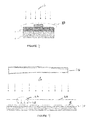
- FIGS. 6 and 7 illustrate an apparatus 14 for producing a beam 16 of electromagnetic radiation.
- the apparatus 14 may be a laser, at least one lamp, or a bank of lamps.
- the substrate 4 has a number of semiconductor devices 20 being fabricated on the substrate 4 . Although twelve semiconductor devices 20 and shown, there may be any suitable number.
- the ohmic contacts 5 are annealed to enable them to be more strongly adhered to the epitaxial layers 1 . This is by a form of fusion of the ohmic contacts 5 and the epitaxial layers 1 at their interface.
- the apparatus 14 produces the beam 16 .
- the beam 16 will be a laser beam if apparatus 14 is a laser, or will be light of desired frequency if apparatus 14 is at least one lamp, or a bank of lamps.
- the beam 16 is focused on the exposed surface of the ohmic contact 5 . As such the ohmic contact 5 is heated by the beam 16 . Due to the inherent heat conductivity of the ohmic contact 5 , the beam 16 does not need to be applied to the entirety of the surface of the ohmic contact 5
- the beam 16 is shown being applied to one semiconductor device 20 . It may be applied to two or more simultaneously, up to being simultaneously applied to all semiconductor devices 20 .
- the heat conductivity of the ohmic contact 5 means that heating is limited to the immediate area 30 of the ohmic contact 5 and thus not all of the epitaxial layers 1 are heated. In this way the heat in the expitaxial layers 1 is dispersed through the epitaxial layers 1 and does not affect the interface of epitaxial layers 1 and the second substrate 4 . Therefore the temperature at the interface of the epitaxial layer 1 and the second substrate 4 will be less that the temperature at the interface of the ohmic contact 5 and the epitaxial layer 1 .
- the duration, wavelength, radiation power, and radiation power density of the application of the electromagnetic beam 16 may be determined by the metal of the at least one metal layer 5 , and the thickness of the at least one metal layer 5 , and the materials of the semiconductor devices 20 .
- FIG. 9 shows a second embodiment. This may be used when the beam 16 is laser beam, but should be used when the beam 16 is of light.
- a mask 24 is placed between source 14 and the semiconductor devices 20 .
- the mask 24 has at least one aperture 26 that is preferably sized and shaped to be substantially the same as that of the area to be annealed—in this case the ohmic contact 5 . In that way the light 28 passing through the aperture 26 only contacts the ohmic contact 5 and not the epitaxial layers 1 .
- localized optical annealing is used in semiconductor device fabrication, where the original wafer substrate is removed and the semiconductor layers are transferred to a new substrate either before or after the optical-annealing.
- Both laser annealing and lamp annealing may be used.
- Laser annealing can be applied to where annealing is required by directing the laser beam to that area.
- a broad light beam that is generated by a lamp, a bank of lamps, or a broadened laser beam can also be applied to the whole surface of the wafer, or to an interface in the wafer if the light is so chosen that it can pass certain layers (or substrate) of the wafer without being significantly absorbed before reaching the interface.
- the above-described process may also be used to anneal a more substantial metal layer such as, for example, the second substrate 4 .
- the second substrate 4 is a layer of a metal (copper) that has high conductivity
- the beam 16 does not need to be applied to the entirety of the metal layer 4 , but is applied sequentially to locations on the surface of the metal layer 4 for annealing of the metal layer 4 to take place.
- the number and spacing of the locations, the duration of the application of the beam 16 at each location, the intensity of the laser beam 16 and the frequency of the laser beam 16 will be determined by the metal of the metal layer 4 , and the thickness of the metal layer 4 .
- the beam 16 may be applied simultaneously to the number of locations.
- the order of application of the beam 16 matches heat flow in the metal layer 4 to maximize the annealing.
- the aperture(s) 26 will be sized, shaped, spaced and located to substantially match the size, shape, spacing and location of the metal layers 4 .
- the beam 16 may be applied directly to the at least one metal layer 22 , or may be applied to the at least one metal layer 22 through the semiconductor device 20 . In the latter case, the beam 16 is preferably applied to the interface between the at least one metal layer 22 and the semiconductor devices 20 .
- each layer may be annealed sequentially, or simultaneously.
- the nature of the beam 16 will depend significantly on the materials of the ohmic or metal layer 5 , and the epitaxial layers 1 . This will include the thickness of the ohmic or metal layer 5 .
- Laser conditions include pulse width of the laser, number of pulses, the frequency of the pulses, and the power and density of the laser beam.
Abstract
Description
Claims (9)
Applications Claiming Priority (4)
| Application Number | Priority Date | Filing Date | Title |
|---|---|---|---|
| SG200508210 | 2005-12-20 | ||
| SG200508210-2A SG133432A1 (en) | 2005-12-20 | 2005-12-20 | Localized annealing during semiconductor device fabrication |
| SG200508210-2 | 2005-12-20 | ||
| PCT/SG2006/000395 WO2007073354A1 (en) | 2005-12-20 | 2006-12-19 | Localized annealing during semiconductor device fabrication |
Publications (2)
| Publication Number | Publication Date |
|---|---|
| US20100047996A1 US20100047996A1 (en) | 2010-02-25 |
| US8329556B2 true US8329556B2 (en) | 2012-12-11 |
Family
ID=38188964
Family Applications (1)
| Application Number | Title | Priority Date | Filing Date |
|---|---|---|---|
| US12/158,678 Expired - Fee Related US8329556B2 (en) | 2005-12-20 | 2006-12-19 | Localized annealing during semiconductor device fabrication |
Country Status (6)
| Country | Link |
|---|---|
| US (1) | US8329556B2 (en) |
| JP (1) | JP2009520376A (en) |
| KR (1) | KR20080096510A (en) |
| CN (1) | CN101410991B (en) |
| SG (1) | SG133432A1 (en) |
| WO (1) | WO2007073354A1 (en) |
Cited By (5)
| Publication number | Priority date | Publication date | Assignee | Title |
|---|---|---|---|---|
| US10170681B1 (en) | 2017-11-28 | 2019-01-01 | International Business Machines Corporation | Laser annealing of qubits with structured illumination |
| US10340438B2 (en) | 2017-11-28 | 2019-07-02 | International Business Machines Corporation | Laser annealing qubits for optimized frequency allocation |
| US10355193B2 (en) | 2017-11-28 | 2019-07-16 | International Business Machines Corporation | Flip chip integration on qubit chips |
| US10418540B2 (en) | 2017-11-28 | 2019-09-17 | International Business Machines Corporation | Adjustment of qubit frequency through annealing |
| US11895931B2 (en) | 2017-11-28 | 2024-02-06 | International Business Machines Corporation | Frequency tuning of multi-qubit systems |
Families Citing this family (8)
| Publication number | Priority date | Publication date | Assignee | Title |
|---|---|---|---|---|
| TWI228272B (en) | 2003-09-19 | 2005-02-21 | Tinggi Technologies Pte Ltd | Fabrication of semiconductor devices |
| EP1730790B1 (en) | 2004-03-15 | 2011-11-09 | Tinggi Technologies Private Limited | Fabrication of semiconductor devices |
| CN1998094B (en) | 2004-04-07 | 2012-12-26 | 霆激技术有限公司 | Fabrication of reflective layer on semiconductor light emitting diodes |
| SG130975A1 (en) | 2005-09-29 | 2007-04-26 | Tinggi Tech Private Ltd | Fabrication of semiconductor devices for light emission |
| SG131803A1 (en) | 2005-10-19 | 2007-05-28 | Tinggi Tech Private Ltd | Fabrication of transistors |
| SG140473A1 (en) | 2006-08-16 | 2008-03-28 | Tinggi Tech Private Ltd | Improvements in external light efficiency of light emitting diodes |
| SG140512A1 (en) | 2006-09-04 | 2008-03-28 | Tinggi Tech Private Ltd | Electrical current distribution in light emitting devices |
| DE102021108756A1 (en) * | 2021-04-08 | 2022-10-13 | Osram Opto Semiconductors Gmbh | METHOD OF TESTING A WAFER AND WAFER |
Citations (134)
| Publication number | Priority date | Publication date | Assignee | Title |
|---|---|---|---|---|
| US3897627A (en) | 1974-06-28 | 1975-08-05 | Rca Corp | Method for manufacturing semiconductor devices |
| US4107720A (en) | 1974-10-29 | 1978-08-15 | Raytheon Company | Overlay metallization multi-channel high frequency field effect transistor |
| US5192987A (en) | 1991-05-17 | 1993-03-09 | Apa Optics, Inc. | High electron mobility transistor with GaN/Alx Ga1-x N heterojunctions |
| US5405804A (en) | 1993-01-22 | 1995-04-11 | Kabushiki Kaisha Toshiba | Method of manufacturing a semiconductor device by laser annealing a metal layer through an insulator |
| US5654228A (en) | 1995-03-17 | 1997-08-05 | Motorola | VCSEL having a self-aligned heat sink and method of making |
| US5719433A (en) | 1995-07-25 | 1998-02-17 | Thomson-Csf | Semiconductor component with integrated heat sink |
| US5811927A (en) | 1996-06-21 | 1998-09-22 | Motorola, Inc. | Method for affixing spacers within a flat panel display |
| US5879862A (en) | 1995-09-30 | 1999-03-09 | Daewoo Electronics Co., Ltd. | Method for planarizing a non planar layer |
| US5917202A (en) * | 1995-12-21 | 1999-06-29 | Hewlett-Packard Company | Highly reflective contacts for light emitting semiconductor devices |
| US6020261A (en) | 1999-06-01 | 2000-02-01 | Motorola, Inc. | Process for forming high aspect ratio circuit features |
| JP2000164928A (en) | 1998-11-25 | 2000-06-16 | Toshiba Electronic Engineering Corp | Semiconductor light emitting device and its manufacture |
| JP2000183400A (en) | 1998-12-17 | 2000-06-30 | Toyoda Gosei Co Ltd | Iii nitride compound semiconductor light-emitting element |
| US6091085A (en) | 1998-02-19 | 2000-07-18 | Agilent Technologies, Inc. | GaN LEDs with improved output coupling efficiency |
| US6117784A (en) | 1997-11-12 | 2000-09-12 | International Business Machines Corporation | Process for integrated circuit wiring |
| JP2000277804A (en) | 1995-06-15 | 2000-10-06 | Nichia Chem Ind Ltd | Nitride semiconductor device and manufacture thereof, and light emitting element |
| JP2000294837A (en) | 1999-04-05 | 2000-10-20 | Stanley Electric Co Ltd | Gallium nitride compound semiconductor light emitting element |
| EP1061590A1 (en) | 1998-12-28 | 2000-12-20 | Shin-Etsu Handotai Co., Ltd | Light emitting diode and its manufacturing method |
| US6169297B1 (en) | 1997-12-23 | 2001-01-02 | Kwangju Institute Of Science And Technology | Metal thin film with ohmic contact for light emit diodes |
| TW419836B (en) | 1998-05-13 | 2001-01-21 | Toyoda Gosei Kk | Flip tip type of light-emitting semiconductor device using group III nitride compound |
| JP2001036129A (en) | 1999-07-16 | 2001-02-09 | Dowa Mining Co Ltd | Light emitting diode and manufacture thereof |
| JP2001035974A (en) | 1999-07-19 | 2001-02-09 | Nec Corp | Semiconductor device, and manufacture thereof |
| JP2001049491A (en) | 1999-08-04 | 2001-02-20 | Fujitsu Ltd | Cu ELECTROPLATING FILM FORMING METHOD |
| US6210479B1 (en) | 1999-02-26 | 2001-04-03 | International Business Machines Corporation | Product and process for forming a semiconductor structure on a host substrate |
| JP2001168387A (en) | 1999-09-29 | 2001-06-22 | Toyoda Gosei Co Ltd | Iii nitride compound semiconductor element |
| JP2001168094A (en) | 1999-12-06 | 2001-06-22 | Murata Mfg Co Ltd | Wiring structure, wiring forming method and semiconductor device |
| WO2001047039A1 (en) | 1999-12-22 | 2001-06-28 | Lumileds Lighting, U.S., Llc | Method of making a iii-nitride light-emitting device with increased light generating capability |
| US6259156B1 (en) | 1998-03-13 | 2001-07-10 | Nec Corporation | Semiconductor device and method for manufacturing same |
| JP2001237461A (en) | 2000-02-22 | 2001-08-31 | Toshiba Corp | Semiconductor light-emitting element |
| KR20010088931A (en) | 2001-08-08 | 2001-09-29 | 유태경 | Fabrication Method of GaN related LED using Substrate Remove Technology |
| EP1139409A2 (en) | 2000-02-29 | 2001-10-04 | Agere Systems Guardian Corporation | Selective laser anneal on semiconductor material |
| JP2001274507A (en) | 2000-03-28 | 2001-10-05 | Pioneer Electronic Corp | Nitride semiconductor laser and its manufacturing method |
| US6303405B1 (en) | 1998-09-25 | 2001-10-16 | Kabushiki Kaisha Toshiba | Semiconductor light emitting element, and its manufacturing method |
| US6307218B1 (en) | 1998-11-20 | 2001-10-23 | Lumileds Lighting, U.S., Llc | Electrode structures for light emitting devices |
| JP2001313422A (en) | 2000-02-21 | 2001-11-09 | Nichia Chem Ind Ltd | Light-emitting element and manufacturing method for the light-emitting element |
| US6319778B1 (en) | 2000-08-10 | 2001-11-20 | United Epitaxy Company, Inc. | Method of making light emitting diode |
| TW475276B (en) | 2000-11-07 | 2002-02-01 | Ind Tech Res Inst | GaN based III-V compound semiconductor light-emitting device |
| US20020022286A1 (en) | 1997-11-18 | 2002-02-21 | Nikolaev Audrey E. | Method for growing p-n heterojunction-based structures utilizing HVPE techniques |
| US20020034835A1 (en) | 2000-09-19 | 2002-03-21 | United Epitaxy Company, Inc. | Method of fabricating high efficiency light-emitting diode with a transparent substrate |
| US6365429B1 (en) | 1998-12-30 | 2002-04-02 | Xerox Corporation | Method for nitride based laser diode with growth substrate removed using an intermediate substrate |
| US6380564B1 (en) | 2000-08-16 | 2002-04-30 | United Epitaxy Company, Ltd. | Semiconductor light emitting device |
| US6420242B1 (en) | 1998-01-23 | 2002-07-16 | The Regents Of The University Of California | Separation of thin films from transparent substrates by selective optical processing |
| US6420732B1 (en) | 2000-06-26 | 2002-07-16 | Luxnet Corporation | Light emitting diode of improved current blocking and light extraction structure |
| US20020093023A1 (en) | 1997-06-03 | 2002-07-18 | Camras Michael D. | III-Phosphide and III-Arsenide flip chip light-emitting devices |
| US6426512B1 (en) | 1999-03-05 | 2002-07-30 | Toyoda Gosei Co., Ltd. | Group III nitride compound semiconductor device |
| US20020113279A1 (en) | 2001-02-19 | 2002-08-22 | Mitsubishi Denki Kabushiki Kaisha | Semiconductor device, and method of forming an electrode |
| KR100338180B1 (en) | 1993-03-19 | 2002-08-24 | 루미리즈 라이팅 유에스 엘엘씨 | Wafer bonding of light emitting diode layers |
| US20020117681A1 (en) | 2001-02-23 | 2002-08-29 | Weeks T. Warren | Gallium nitride material devices and methods including backside vias |
| US6455870B1 (en) | 1999-06-15 | 2002-09-24 | Arima Optoelectronics Corporation | Unipolar light emitting devices based on III-nitride semiconductor superlattices |
| US20020137243A1 (en) | 2001-03-22 | 2002-09-26 | Nai-Chuan Chen | Method for forming a semiconductor device having a metallic substrate |
| US20020134985A1 (en) | 2000-08-01 | 2002-09-26 | Tzer-Perng Chen | Interface texturing for light-emitting device |
| CN1373522A (en) | 2001-03-05 | 2002-10-09 | 全新光电科技股份有限公司 | LED with substrate coated with metallic reflection film and its preparing process |
| US20020179910A1 (en) | 2001-03-15 | 2002-12-05 | Slater David B. | Low temperature formation of backside ohmic contacts for vertical devices |
| US6492661B1 (en) | 1999-11-04 | 2002-12-10 | Fen-Ren Chien | Light emitting semiconductor device having reflection layer structure |
| US6509270B1 (en) | 2001-03-30 | 2003-01-21 | Cypress Semiconductor Corp. | Method for polishing a semiconductor topography |
| US20030038284A1 (en) | 2000-06-21 | 2003-02-27 | Sharp Kabushiki Kaisha | Semiconductor light emitting device for stably obtaining peak wave length of emission spectrum |
| US20030064535A1 (en) | 2001-09-28 | 2003-04-03 | Kub Francis J. | Method of manufacturing a semiconductor device having a thin GaN material directly bonded to an optimized substrate |
| US6562648B1 (en) | 2000-08-23 | 2003-05-13 | Xerox Corporation | Structure and method for separation and transfer of semiconductor thin films onto dissimilar substrate materials |
| JP2003152138A (en) | 2001-11-08 | 2003-05-23 | Furukawa Electric Co Ltd:The | Semiconductor device excellent in heat dissipation |
| US6573537B1 (en) | 1999-12-22 | 2003-06-03 | Lumileds Lighting, U.S., Llc | Highly reflective ohmic contacts to III-nitride flip-chip LEDs |
| US20030111667A1 (en) | 2001-12-13 | 2003-06-19 | Schubert E. Fred | Light-emitting diode with planar omni-directional reflector |
| TW540171B (en) | 2002-07-18 | 2003-07-01 | United Epitaxy Co Ltd | Manufacturing method of high-power light emitting diode |
| US6589857B2 (en) | 2001-03-23 | 2003-07-08 | Matsushita Electric Industrial Co., Ltd. | Manufacturing method of semiconductor film |
| EP1326290A2 (en) | 2001-12-21 | 2003-07-09 | Xerox Corporation | Method of fabricating semiconductor structures |
| JP2003218383A (en) | 2002-01-18 | 2003-07-31 | Toshiba Corp | Semiconductor light emitting element and its manufacturing method |
| US20030151357A1 (en) | 2002-02-12 | 2003-08-14 | Toyoda Gosei Co., Ltd. | Group III nitride compound semiconductor light emitting element |
| US20030189212A1 (en) | 2002-04-09 | 2003-10-09 | Yoo Myung Cheol | Method of fabricating vertical devices using a metal support film |
| US20030189215A1 (en) | 2002-04-09 | 2003-10-09 | Jong-Lam Lee | Method of fabricating vertical structure leds |
| JP2003303743A (en) | 2002-04-08 | 2003-10-24 | Matsushita Electric Ind Co Ltd | Manufacturing method of nitride semiconductor device and its substrate |
| JP2003309286A (en) | 2002-04-17 | 2003-10-31 | Sharp Corp | Nitride semiconductor light-emitting element and its manufacturing method |
| JP2003318443A (en) | 2002-04-23 | 2003-11-07 | Sharp Corp | Nitride based semiconductor light emitting element and its fabricating method |
| US6649437B1 (en) | 2002-08-20 | 2003-11-18 | United Epitaxy Company, Ltd. | Method of manufacturing high-power light emitting diodes |
| JP2003347590A (en) | 2002-05-29 | 2003-12-05 | Matsushita Electric Ind Co Ltd | Fabrication method of semiconductor device |
| US20040026709A1 (en) | 2000-04-26 | 2004-02-12 | Stefan Bader | Gan-based light emitting-diode chip and a method for producing a luminescent diode component |
| US20040033638A1 (en) | 2000-10-17 | 2004-02-19 | Stefan Bader | Method for fabricating a semiconductor component based on GaN |
| JP2004072052A (en) | 2002-08-09 | 2004-03-04 | Matsushita Electric Ind Co Ltd | Semiconductor device and manufacturing method thereof |
| US20040065889A1 (en) | 2002-06-10 | 2004-04-08 | Matsushita Electric Industrial Co., Ltd. | Semiconductor wafer, semiconductor device, and methods for fabricating the same |
| US20040104395A1 (en) | 2002-11-28 | 2004-06-03 | Shin-Etsu Handotai Co., Ltd. | Light-emitting device, method of fabricating the same, and OHMIC electrode structure for semiconductor device |
| US20040110395A1 (en) | 2002-05-23 | 2004-06-10 | Matsushita Electric Industrial Co., Ltd. | Method for fabricating semiconductor device |
| KR20040058479A (en) | 2002-12-27 | 2004-07-05 | 삼성전기주식회사 | VERTICAL GaN LIGHT EMITTING DIODE AND METHOD OF PRODUCING THE SAME |
| US20040130037A1 (en) | 2003-01-02 | 2004-07-08 | Cree Lighting Company | Group III nitride based flip-chip intergrated circuit and method for fabricating |
| US20040144991A1 (en) | 2003-01-15 | 2004-07-29 | Fujitsu Limited | Compound semiconductor device and method for fabricating the same |
| US20040217362A1 (en) | 2001-02-01 | 2004-11-04 | Slater David B | Light emitting diodes including pedestals |
| JP2004319552A (en) | 2003-04-11 | 2004-11-11 | Nichia Chem Ind Ltd | Flip-chip counter-electrode hemt |
| US6821804B2 (en) | 1999-12-03 | 2004-11-23 | Cree, Inc. | Enhanced light extraction in LEDs through the use of internal and external optical elements |
| WO2004102686A1 (en) | 2003-05-09 | 2004-11-25 | Cree, Inc. | Led fabrication via ion implant isolation |
| US20040235210A1 (en) | 2003-05-22 | 2004-11-25 | Matsushita Electric Industrial Co. Ltd. | Method for fabricating semiconductor devices |
| KR20040104232A (en) | 2003-06-03 | 2004-12-10 | 삼성전기주식회사 | A METHOD OF PRODUCING VERTICAL GaN LIGHT EMITTING DIODES |
| JP2005012188A (en) | 2003-05-22 | 2005-01-13 | Matsushita Electric Ind Co Ltd | Manufacturing method for semiconductor device |
| US20050014303A1 (en) | 2003-06-18 | 2005-01-20 | United Epitaxy Company, Ltd. | Method for manufacturing semiconductor light-emitting device |
| US20050026399A1 (en) | 2003-08-02 | 2005-02-03 | Fen-Ren Chien | Light emitting diode structure and manufacture method thereof |
| US20050035354A1 (en) | 2003-08-14 | 2005-02-17 | Dicon Fiberoptics, Inc | Light emiting diodes with current spreading layer |
| WO2005029572A1 (en) | 2003-09-19 | 2005-03-31 | Tinggi Technologies Private Limited | Fabrication of conductive metal layer on semiconductor devices |
| WO2005029573A1 (en) | 2003-09-19 | 2005-03-31 | Tinggi Technologies Private Limited | Fabrication of semiconductor devices |
| US20050082555A1 (en) | 2003-10-15 | 2005-04-21 | United Epitaxy Company, Ltd. | Light-emitting semiconductor device having enhanced brightness |
| US20050087884A1 (en) | 2003-10-24 | 2005-04-28 | Stokes Edward B. | Flip-chip light emitting diode |
| US20050093002A1 (en) | 2003-10-30 | 2005-05-05 | United Epitaxy Company, Ltd. | Light emitting diode device and manufacturing method |
| US20050127397A1 (en) | 2001-02-23 | 2005-06-16 | Nitronex Corporation | Gallium nitride materials including thermally conductive regions |
| US20050142875A1 (en) | 2003-10-01 | 2005-06-30 | Yoo Woo S. | Selective heating using flash anneal |
| WO2005062745A2 (en) | 2003-10-10 | 2005-07-14 | The Regents Of The University Of California | GaN/AlGaN/GaN DISPERSION-FREE HIGH ELECTRON MOBILITY TRANSISTORS |
| WO2005064666A1 (en) | 2003-12-09 | 2005-07-14 | The Regents Of The University Of California | Highly efficient gallium nitride based light emitting diodes via surface roughening |
| US20050164482A1 (en) | 2004-01-22 | 2005-07-28 | Cree, Inc. | Silicon Carbide on Diamond Substrates and Related Devices and Methods |
| JP2005236048A (en) | 2004-02-19 | 2005-09-02 | Shin Etsu Handotai Co Ltd | GaP EPITAXIAL WAFER AND GaP LIGHT EMITTING ELEMENT |
| JP2005260255A (en) | 1996-02-19 | 2005-09-22 | Sharp Corp | Compound semiconductor device and method for manufacturing the same |
| WO2005088743A1 (en) | 2004-03-15 | 2005-09-22 | Tinggi Technologies Private Limited | Fabrication of semiconductor devices |
| US20050208435A1 (en) | 2004-03-19 | 2005-09-22 | Irene Chen | Method for fabricating metallic structure |
| JP2005286187A (en) | 2004-03-30 | 2005-10-13 | Denso Corp | Semiconductor device |
| WO2005096365A1 (en) | 2004-03-30 | 2005-10-13 | Nec Corporation | Semiconductor device |
| WO2005098974A1 (en) | 2004-04-07 | 2005-10-20 | Tinggi Technologies Private Limited | Fabrication of reflective layer on semiconductor light emitting diodes |
| WO2005104780A2 (en) | 2004-04-28 | 2005-11-10 | Verticle, Inc | Vertical structure semiconductor devices |
| US20060002442A1 (en) | 2004-06-30 | 2006-01-05 | Kevin Haberern | Light emitting devices having current blocking structures and methods of fabricating light emitting devices having current blocking structures |
| US20060006554A1 (en) | 2004-06-22 | 2006-01-12 | Yoo Myung C | Vertical structure semiconductor devices with improved light output |
| US20060124939A1 (en) | 2004-12-13 | 2006-06-15 | Lee Jae S | Method for manufacturing GaN-based light emitting diode using laser lift-off technique and light emitting diode manufactured thereby |
| US20060154389A1 (en) | 2005-01-11 | 2006-07-13 | Doan Trung T | Light emitting diode with conducting metal substrate |
| US20060154390A1 (en) | 2005-01-11 | 2006-07-13 | Tran Chuong A | Systems and methods for producing light emitting diode array |
| US20060151801A1 (en) | 2005-01-11 | 2006-07-13 | Doan Trung T | Light emitting diode with thermo-electric cooler |
| US20060154393A1 (en) | 2005-01-11 | 2006-07-13 | Doan Trung T | Systems and methods for removing operating heat from a light emitting diode |
| US20060154391A1 (en) | 2005-01-11 | 2006-07-13 | Tran Chuong A | Light emitting diodes (LEDs) with improved light extraction by roughening |
| US20060154392A1 (en) | 2005-01-11 | 2006-07-13 | Tran Chuong A | Method of making a vertical light emitting diode |
| US20060157721A1 (en) | 2005-01-11 | 2006-07-20 | Tran Chuong A | Systems and methods for producing white-light light emitting diodes |
| US20060163586A1 (en) | 2005-01-24 | 2006-07-27 | Cree, Inc. | LED with current confinement structure and surface roughening |
| EP1693891A2 (en) | 2005-01-31 | 2006-08-23 | Interuniversitair Micro-Elektronica Centrum (IMEC) | Method of manufacturing a semiconductor device |
| US20060186418A1 (en) | 2004-05-18 | 2006-08-24 | Edmond John A | External extraction light emitting diode based upon crystallographic faceted surfaces |
| JP2006253647A (en) | 2005-02-08 | 2006-09-21 | Rohm Co Ltd | Semiconductor light emitting element and manufacturing method |
| US7166861B2 (en) * | 2003-01-23 | 2007-01-23 | Dai Nippon Printing Co., Ltd. | Thin-film transistor and method for manufacturing the same |
| US20070029541A1 (en) | 2005-08-04 | 2007-02-08 | Huoping Xin | High efficiency light emitting device |
| WO2007037762A1 (en) | 2005-09-29 | 2007-04-05 | Tinggi Technologies Private Limited | Fabrication of semiconductor devices for light emission |
| WO2007046773A1 (en) | 2005-10-19 | 2007-04-26 | Tinggi Technologies Private Limited | Fabrication of transistors |
| WO2008020819A1 (en) | 2006-08-16 | 2008-02-21 | Tinggi Technologies Private Limited | Improvements in external light efficiency of light emitting diodes |
| WO2008030188A1 (en) | 2006-09-04 | 2008-03-13 | Tinggi Technologies Private Limited | Electrical current distribution in light emitting devices |
| US7348212B2 (en) | 2005-09-13 | 2008-03-25 | Philips Lumileds Lighting Company Llc | Interconnects for semiconductor light emitting devices |
| US20080105303A1 (en) * | 2003-01-03 | 2008-05-08 | Bp Corporation North America Inc. | Method and Manufacturing Thin Film Photovoltaic Modules |
| US20080265366A1 (en) | 2006-04-25 | 2008-10-30 | Texas Instruments Incorporated | Semiconductor device with improved contact fuse |
| JP2004088083A5 (en) | 2003-06-20 | 2009-03-12 | ||
| US7547578B2 (en) * | 2005-09-16 | 2009-06-16 | Cree, Inc. | Methods of processing semiconductor wafers having silicon carbide power devices thereon |
Family Cites Families (1)
| Publication number | Priority date | Publication date | Assignee | Title |
|---|---|---|---|---|
| JP2004088083A (en) | 2002-06-25 | 2004-03-18 | Matsushita Electric Ind Co Ltd | Semiconductor light emitting device, its manufacturing method, and its packaging method |
-
2005
- 2005-12-20 SG SG200508210-2A patent/SG133432A1/en unknown
-
2006
- 2006-12-19 WO PCT/SG2006/000395 patent/WO2007073354A1/en active Application Filing
- 2006-12-19 JP JP2008547189A patent/JP2009520376A/en not_active Withdrawn
- 2006-12-19 KR KR1020087017343A patent/KR20080096510A/en not_active Application Discontinuation
- 2006-12-19 CN CN2006800481382A patent/CN101410991B/en not_active Expired - Fee Related
- 2006-12-19 US US12/158,678 patent/US8329556B2/en not_active Expired - Fee Related
Patent Citations (158)
| Publication number | Priority date | Publication date | Assignee | Title |
|---|---|---|---|---|
| US3897627A (en) | 1974-06-28 | 1975-08-05 | Rca Corp | Method for manufacturing semiconductor devices |
| US4107720A (en) | 1974-10-29 | 1978-08-15 | Raytheon Company | Overlay metallization multi-channel high frequency field effect transistor |
| US5192987A (en) | 1991-05-17 | 1993-03-09 | Apa Optics, Inc. | High electron mobility transistor with GaN/Alx Ga1-x N heterojunctions |
| US5405804A (en) | 1993-01-22 | 1995-04-11 | Kabushiki Kaisha Toshiba | Method of manufacturing a semiconductor device by laser annealing a metal layer through an insulator |
| KR100338180B1 (en) | 1993-03-19 | 2002-08-24 | 루미리즈 라이팅 유에스 엘엘씨 | Wafer bonding of light emitting diode layers |
| US5654228A (en) | 1995-03-17 | 1997-08-05 | Motorola | VCSEL having a self-aligned heat sink and method of making |
| JP2000277804A (en) | 1995-06-15 | 2000-10-06 | Nichia Chem Ind Ltd | Nitride semiconductor device and manufacture thereof, and light emitting element |
| US5719433A (en) | 1995-07-25 | 1998-02-17 | Thomson-Csf | Semiconductor component with integrated heat sink |
| US5879862A (en) | 1995-09-30 | 1999-03-09 | Daewoo Electronics Co., Ltd. | Method for planarizing a non planar layer |
| US5917202A (en) * | 1995-12-21 | 1999-06-29 | Hewlett-Packard Company | Highly reflective contacts for light emitting semiconductor devices |
| JP2005260255A (en) | 1996-02-19 | 2005-09-22 | Sharp Corp | Compound semiconductor device and method for manufacturing the same |
| US5811927A (en) | 1996-06-21 | 1998-09-22 | Motorola, Inc. | Method for affixing spacers within a flat panel display |
| US20020093023A1 (en) | 1997-06-03 | 2002-07-18 | Camras Michael D. | III-Phosphide and III-Arsenide flip chip light-emitting devices |
| US6117784A (en) | 1997-11-12 | 2000-09-12 | International Business Machines Corporation | Process for integrated circuit wiring |
| US20020022286A1 (en) | 1997-11-18 | 2002-02-21 | Nikolaev Audrey E. | Method for growing p-n heterojunction-based structures utilizing HVPE techniques |
| US6169297B1 (en) | 1997-12-23 | 2001-01-02 | Kwangju Institute Of Science And Technology | Metal thin film with ohmic contact for light emit diodes |
| US6420242B1 (en) | 1998-01-23 | 2002-07-16 | The Regents Of The University Of California | Separation of thin films from transparent substrates by selective optical processing |
| US6091085A (en) | 1998-02-19 | 2000-07-18 | Agilent Technologies, Inc. | GaN LEDs with improved output coupling efficiency |
| US6627989B2 (en) | 1998-03-13 | 2003-09-30 | Nec Electronics Corporation | Semiconductor device and method for manufacturing same |
| US6259156B1 (en) | 1998-03-13 | 2001-07-10 | Nec Corporation | Semiconductor device and method for manufacturing same |
| TW419836B (en) | 1998-05-13 | 2001-01-21 | Toyoda Gosei Kk | Flip tip type of light-emitting semiconductor device using group III nitride compound |
| US6303405B1 (en) | 1998-09-25 | 2001-10-16 | Kabushiki Kaisha Toshiba | Semiconductor light emitting element, and its manufacturing method |
| US6307218B1 (en) | 1998-11-20 | 2001-10-23 | Lumileds Lighting, U.S., Llc | Electrode structures for light emitting devices |
| JP2000164928A (en) | 1998-11-25 | 2000-06-16 | Toshiba Electronic Engineering Corp | Semiconductor light emitting device and its manufacture |
| JP2000183400A (en) | 1998-12-17 | 2000-06-30 | Toyoda Gosei Co Ltd | Iii nitride compound semiconductor light-emitting element |
| EP1061590A1 (en) | 1998-12-28 | 2000-12-20 | Shin-Etsu Handotai Co., Ltd | Light emitting diode and its manufacturing method |
| US6448102B1 (en) | 1998-12-30 | 2002-09-10 | Xerox Corporation | Method for nitride based laser diode with growth substrate removed |
| US6365429B1 (en) | 1998-12-30 | 2002-04-02 | Xerox Corporation | Method for nitride based laser diode with growth substrate removed using an intermediate substrate |
| US6210479B1 (en) | 1999-02-26 | 2001-04-03 | International Business Machines Corporation | Product and process for forming a semiconductor structure on a host substrate |
| US6426512B1 (en) | 1999-03-05 | 2002-07-30 | Toyoda Gosei Co., Ltd. | Group III nitride compound semiconductor device |
| JP2000294837A (en) | 1999-04-05 | 2000-10-20 | Stanley Electric Co Ltd | Gallium nitride compound semiconductor light emitting element |
| US6020261A (en) | 1999-06-01 | 2000-02-01 | Motorola, Inc. | Process for forming high aspect ratio circuit features |
| US6455870B1 (en) | 1999-06-15 | 2002-09-24 | Arima Optoelectronics Corporation | Unipolar light emitting devices based on III-nitride semiconductor superlattices |
| JP2001036129A (en) | 1999-07-16 | 2001-02-09 | Dowa Mining Co Ltd | Light emitting diode and manufacture thereof |
| JP2001035974A (en) | 1999-07-19 | 2001-02-09 | Nec Corp | Semiconductor device, and manufacture thereof |
| JP2001049491A (en) | 1999-08-04 | 2001-02-20 | Fujitsu Ltd | Cu ELECTROPLATING FILM FORMING METHOD |
| JP2001168387A (en) | 1999-09-29 | 2001-06-22 | Toyoda Gosei Co Ltd | Iii nitride compound semiconductor element |
| US6492661B1 (en) | 1999-11-04 | 2002-12-10 | Fen-Ren Chien | Light emitting semiconductor device having reflection layer structure |
| US6821804B2 (en) | 1999-12-03 | 2004-11-23 | Cree, Inc. | Enhanced light extraction in LEDs through the use of internal and external optical elements |
| JP2001168094A (en) | 1999-12-06 | 2001-06-22 | Murata Mfg Co Ltd | Wiring structure, wiring forming method and semiconductor device |
| WO2001047039A1 (en) | 1999-12-22 | 2001-06-28 | Lumileds Lighting, U.S., Llc | Method of making a iii-nitride light-emitting device with increased light generating capability |
| US6573537B1 (en) | 1999-12-22 | 2003-06-03 | Lumileds Lighting, U.S., Llc | Highly reflective ohmic contacts to III-nitride flip-chip LEDs |
| JP2001313422A (en) | 2000-02-21 | 2001-11-09 | Nichia Chem Ind Ltd | Light-emitting element and manufacturing method for the light-emitting element |
| JP2001237461A (en) | 2000-02-22 | 2001-08-31 | Toshiba Corp | Semiconductor light-emitting element |
| EP1139409A2 (en) | 2000-02-29 | 2001-10-04 | Agere Systems Guardian Corporation | Selective laser anneal on semiconductor material |
| JP2001274507A (en) | 2000-03-28 | 2001-10-05 | Pioneer Electronic Corp | Nitride semiconductor laser and its manufacturing method |
| US6677173B2 (en) | 2000-03-28 | 2004-01-13 | Pioneer Corporation | Method of manufacturing a nitride semiconductor laser with a plated auxiliary metal substrate |
| US20010055324A1 (en) | 2000-03-28 | 2001-12-27 | Hiroyuki Ota | Nitride semiconductor laser and method of manufacturing the same |
| US20040026709A1 (en) | 2000-04-26 | 2004-02-12 | Stefan Bader | Gan-based light emitting-diode chip and a method for producing a luminescent diode component |
| US20030038284A1 (en) | 2000-06-21 | 2003-02-27 | Sharp Kabushiki Kaisha | Semiconductor light emitting device for stably obtaining peak wave length of emission spectrum |
| US6420732B1 (en) | 2000-06-26 | 2002-07-16 | Luxnet Corporation | Light emitting diode of improved current blocking and light extraction structure |
| US20020134985A1 (en) | 2000-08-01 | 2002-09-26 | Tzer-Perng Chen | Interface texturing for light-emitting device |
| US6586875B1 (en) | 2000-08-10 | 2003-07-01 | United Epitaxy Company, Inc. | Light emitting diode with low-temperature solder layer |
| US6319778B1 (en) | 2000-08-10 | 2001-11-20 | United Epitaxy Company, Inc. | Method of making light emitting diode |
| US6380564B1 (en) | 2000-08-16 | 2002-04-30 | United Epitaxy Company, Ltd. | Semiconductor light emitting device |
| US6627921B2 (en) | 2000-08-23 | 2003-09-30 | Xerox Corporation | Structure and method for separation and transfer of semiconductor thin films onto dissimilar substrate materials |
| US6562648B1 (en) | 2000-08-23 | 2003-05-13 | Xerox Corporation | Structure and method for separation and transfer of semiconductor thin films onto dissimilar substrate materials |
| US20020034835A1 (en) | 2000-09-19 | 2002-03-21 | United Epitaxy Company, Inc. | Method of fabricating high efficiency light-emitting diode with a transparent substrate |
| US20040033638A1 (en) | 2000-10-17 | 2004-02-19 | Stefan Bader | Method for fabricating a semiconductor component based on GaN |
| TW475276B (en) | 2000-11-07 | 2002-02-01 | Ind Tech Res Inst | GaN based III-V compound semiconductor light-emitting device |
| US20040217362A1 (en) | 2001-02-01 | 2004-11-04 | Slater David B | Light emitting diodes including pedestals |
| US20020113279A1 (en) | 2001-02-19 | 2002-08-22 | Mitsubishi Denki Kabushiki Kaisha | Semiconductor device, and method of forming an electrode |
| US20050127397A1 (en) | 2001-02-23 | 2005-06-16 | Nitronex Corporation | Gallium nitride materials including thermally conductive regions |
| US20020117681A1 (en) | 2001-02-23 | 2002-08-29 | Weeks T. Warren | Gallium nitride material devices and methods including backside vias |
| CN1373522A (en) | 2001-03-05 | 2002-10-09 | 全新光电科技股份有限公司 | LED with substrate coated with metallic reflection film and its preparing process |
| US20020179910A1 (en) | 2001-03-15 | 2002-12-05 | Slater David B. | Low temperature formation of backside ohmic contacts for vertical devices |
| US20020137243A1 (en) | 2001-03-22 | 2002-09-26 | Nai-Chuan Chen | Method for forming a semiconductor device having a metallic substrate |
| US6589857B2 (en) | 2001-03-23 | 2003-07-08 | Matsushita Electric Industrial Co., Ltd. | Manufacturing method of semiconductor film |
| US6509270B1 (en) | 2001-03-30 | 2003-01-21 | Cypress Semiconductor Corp. | Method for polishing a semiconductor topography |
| KR20010088931A (en) | 2001-08-08 | 2001-09-29 | 유태경 | Fabrication Method of GaN related LED using Substrate Remove Technology |
| US20030064535A1 (en) | 2001-09-28 | 2003-04-03 | Kub Francis J. | Method of manufacturing a semiconductor device having a thin GaN material directly bonded to an optimized substrate |
| JP2003152138A (en) | 2001-11-08 | 2003-05-23 | Furukawa Electric Co Ltd:The | Semiconductor device excellent in heat dissipation |
| US20030111667A1 (en) | 2001-12-13 | 2003-06-19 | Schubert E. Fred | Light-emitting diode with planar omni-directional reflector |
| EP1326290A2 (en) | 2001-12-21 | 2003-07-09 | Xerox Corporation | Method of fabricating semiconductor structures |
| US20030178626A1 (en) | 2002-01-18 | 2003-09-25 | Hitoshi Sugiyama | Semiconductor light-emitting element and method of manufacturing the same |
| JP2003218383A (en) | 2002-01-18 | 2003-07-31 | Toshiba Corp | Semiconductor light emitting element and its manufacturing method |
| US20030151357A1 (en) | 2002-02-12 | 2003-08-14 | Toyoda Gosei Co., Ltd. | Group III nitride compound semiconductor light emitting element |
| JP2003303743A (en) | 2002-04-08 | 2003-10-24 | Matsushita Electric Ind Co Ltd | Manufacturing method of nitride semiconductor device and its substrate |
| US20030189215A1 (en) | 2002-04-09 | 2003-10-09 | Jong-Lam Lee | Method of fabricating vertical structure leds |
| US20030189212A1 (en) | 2002-04-09 | 2003-10-09 | Yoo Myung Cheol | Method of fabricating vertical devices using a metal support film |
| WO2003088320A2 (en) | 2002-04-09 | 2003-10-23 | Oriol, Inc. | A method of fabricating vertical devices using a metal support film |
| US20050098792A1 (en) | 2002-04-09 | 2005-05-12 | Jong-Lam Lee | Method of fabricating vertical structure LEDs |
| EP1502284A2 (en) | 2002-04-09 | 2005-02-02 | Oriol, Inc. | A method of fabricating vertical devices using a metal support film |
| US20060099730A1 (en) | 2002-04-09 | 2006-05-11 | Lg Electronics Inc. | Method of fabricating vertical structure LEDs |
| US20040031967A1 (en) | 2002-04-17 | 2004-02-19 | Mayuko Fudeta | Nitride-based semiconductor light-emitting device and manufacturing method thereof |
| JP2003309286A (en) | 2002-04-17 | 2003-10-31 | Sharp Corp | Nitride semiconductor light-emitting element and its manufacturing method |
| US20030218179A1 (en) | 2002-04-23 | 2003-11-27 | Sharp Kabushiki Kaisha | Nitride-based semiconductor light-emitting device and manufacturing method thereof |
| JP2003318443A (en) | 2002-04-23 | 2003-11-07 | Sharp Corp | Nitride based semiconductor light emitting element and its fabricating method |
| US20040110395A1 (en) | 2002-05-23 | 2004-06-10 | Matsushita Electric Industrial Co., Ltd. | Method for fabricating semiconductor device |
| JP2003347590A (en) | 2002-05-29 | 2003-12-05 | Matsushita Electric Ind Co Ltd | Fabrication method of semiconductor device |
| US20040065889A1 (en) | 2002-06-10 | 2004-04-08 | Matsushita Electric Industrial Co., Ltd. | Semiconductor wafer, semiconductor device, and methods for fabricating the same |
| TW540171B (en) | 2002-07-18 | 2003-07-01 | United Epitaxy Co Ltd | Manufacturing method of high-power light emitting diode |
| JP2004072052A (en) | 2002-08-09 | 2004-03-04 | Matsushita Electric Ind Co Ltd | Semiconductor device and manufacturing method thereof |
| US6649437B1 (en) | 2002-08-20 | 2003-11-18 | United Epitaxy Company, Ltd. | Method of manufacturing high-power light emitting diodes |
| US20040104395A1 (en) | 2002-11-28 | 2004-06-03 | Shin-Etsu Handotai Co., Ltd. | Light-emitting device, method of fabricating the same, and OHMIC electrode structure for semiconductor device |
| KR20040058479A (en) | 2002-12-27 | 2004-07-05 | 삼성전기주식회사 | VERTICAL GaN LIGHT EMITTING DIODE AND METHOD OF PRODUCING THE SAME |
| US20050173692A1 (en) | 2002-12-27 | 2005-08-11 | Park Young H. | Vertical GaN light emitting diode and method for manufacturing the same |
| US20040130037A1 (en) | 2003-01-02 | 2004-07-08 | Cree Lighting Company | Group III nitride based flip-chip intergrated circuit and method for fabricating |
| US20080105303A1 (en) * | 2003-01-03 | 2008-05-08 | Bp Corporation North America Inc. | Method and Manufacturing Thin Film Photovoltaic Modules |
| US20040144991A1 (en) | 2003-01-15 | 2004-07-29 | Fujitsu Limited | Compound semiconductor device and method for fabricating the same |
| US7166861B2 (en) * | 2003-01-23 | 2007-01-23 | Dai Nippon Printing Co., Ltd. | Thin-film transistor and method for manufacturing the same |
| JP2004319552A (en) | 2003-04-11 | 2004-11-11 | Nichia Chem Ind Ltd | Flip-chip counter-electrode hemt |
| WO2004102686A1 (en) | 2003-05-09 | 2004-11-25 | Cree, Inc. | Led fabrication via ion implant isolation |
| US7338822B2 (en) | 2003-05-09 | 2008-03-04 | Cree, Inc. | LED fabrication via ion implant isolation |
| US20040235210A1 (en) | 2003-05-22 | 2004-11-25 | Matsushita Electric Industrial Co. Ltd. | Method for fabricating semiconductor devices |
| JP2005012188A (en) | 2003-05-22 | 2005-01-13 | Matsushita Electric Ind Co Ltd | Manufacturing method for semiconductor device |
| KR20040104232A (en) | 2003-06-03 | 2004-12-10 | 삼성전기주식회사 | A METHOD OF PRODUCING VERTICAL GaN LIGHT EMITTING DIODES |
| US20050014303A1 (en) | 2003-06-18 | 2005-01-20 | United Epitaxy Company, Ltd. | Method for manufacturing semiconductor light-emitting device |
| JP2004088083A5 (en) | 2003-06-20 | 2009-03-12 | ||
| US20050026399A1 (en) | 2003-08-02 | 2005-02-03 | Fen-Ren Chien | Light emitting diode structure and manufacture method thereof |
| US20050035354A1 (en) | 2003-08-14 | 2005-02-17 | Dicon Fiberoptics, Inc | Light emiting diodes with current spreading layer |
| WO2005029573A1 (en) | 2003-09-19 | 2005-03-31 | Tinggi Technologies Private Limited | Fabrication of semiconductor devices |
| WO2005029572A1 (en) | 2003-09-19 | 2005-03-31 | Tinggi Technologies Private Limited | Fabrication of conductive metal layer on semiconductor devices |
| US20080164480A1 (en) | 2003-09-19 | 2008-07-10 | Xuejun Kang | Fabrication of Semiconductor Devices |
| US20080210970A1 (en) | 2003-09-19 | 2008-09-04 | Tinggi Technologies Private Limited | Fabrication of Conductive Metal Layer on Semiconductor Devices |
| US8034643B2 (en) | 2003-09-19 | 2011-10-11 | Tinggi Technologies Private Limited | Method for fabrication of a semiconductor device |
| US20050142875A1 (en) | 2003-10-01 | 2005-06-30 | Yoo Woo S. | Selective heating using flash anneal |
| WO2005062745A2 (en) | 2003-10-10 | 2005-07-14 | The Regents Of The University Of California | GaN/AlGaN/GaN DISPERSION-FREE HIGH ELECTRON MOBILITY TRANSISTORS |
| US20050082555A1 (en) | 2003-10-15 | 2005-04-21 | United Epitaxy Company, Ltd. | Light-emitting semiconductor device having enhanced brightness |
| US20050087884A1 (en) | 2003-10-24 | 2005-04-28 | Stokes Edward B. | Flip-chip light emitting diode |
| US20050093002A1 (en) | 2003-10-30 | 2005-05-05 | United Epitaxy Company, Ltd. | Light emitting diode device and manufacturing method |
| WO2005064666A1 (en) | 2003-12-09 | 2005-07-14 | The Regents Of The University Of California | Highly efficient gallium nitride based light emitting diodes via surface roughening |
| US20050164482A1 (en) | 2004-01-22 | 2005-07-28 | Cree, Inc. | Silicon Carbide on Diamond Substrates and Related Devices and Methods |
| JP2005236048A (en) | 2004-02-19 | 2005-09-02 | Shin Etsu Handotai Co Ltd | GaP EPITAXIAL WAFER AND GaP LIGHT EMITTING ELEMENT |
| US7763477B2 (en) | 2004-03-15 | 2010-07-27 | Tinggi Technologies Pte Limited | Fabrication of semiconductor devices |
| WO2005088743A1 (en) | 2004-03-15 | 2005-09-22 | Tinggi Technologies Private Limited | Fabrication of semiconductor devices |
| US20050208435A1 (en) | 2004-03-19 | 2005-09-22 | Irene Chen | Method for fabricating metallic structure |
| JP2005286187A (en) | 2004-03-30 | 2005-10-13 | Denso Corp | Semiconductor device |
| WO2005096365A1 (en) | 2004-03-30 | 2005-10-13 | Nec Corporation | Semiconductor device |
| US20080121908A1 (en) | 2004-04-07 | 2008-05-29 | Shu Yuan | Fabrication of Reflective Layer on Semconductor Light Emitting Devices |
| WO2005098974A1 (en) | 2004-04-07 | 2005-10-20 | Tinggi Technologies Private Limited | Fabrication of reflective layer on semiconductor light emitting diodes |
| WO2005104780A2 (en) | 2004-04-28 | 2005-11-10 | Verticle, Inc | Vertical structure semiconductor devices |
| US20060186418A1 (en) | 2004-05-18 | 2006-08-24 | Edmond John A | External extraction light emitting diode based upon crystallographic faceted surfaces |
| US20060006554A1 (en) | 2004-06-22 | 2006-01-12 | Yoo Myung C | Vertical structure semiconductor devices with improved light output |
| US20060002442A1 (en) | 2004-06-30 | 2006-01-05 | Kevin Haberern | Light emitting devices having current blocking structures and methods of fabricating light emitting devices having current blocking structures |
| US20060124939A1 (en) | 2004-12-13 | 2006-06-15 | Lee Jae S | Method for manufacturing GaN-based light emitting diode using laser lift-off technique and light emitting diode manufactured thereby |
| US20060154393A1 (en) | 2005-01-11 | 2006-07-13 | Doan Trung T | Systems and methods for removing operating heat from a light emitting diode |
| US20060154391A1 (en) | 2005-01-11 | 2006-07-13 | Tran Chuong A | Light emitting diodes (LEDs) with improved light extraction by roughening |
| US20060151801A1 (en) | 2005-01-11 | 2006-07-13 | Doan Trung T | Light emitting diode with thermo-electric cooler |
| US20060157721A1 (en) | 2005-01-11 | 2006-07-20 | Tran Chuong A | Systems and methods for producing white-light light emitting diodes |
| US20060154392A1 (en) | 2005-01-11 | 2006-07-13 | Tran Chuong A | Method of making a vertical light emitting diode |
| US20060154389A1 (en) | 2005-01-11 | 2006-07-13 | Doan Trung T | Light emitting diode with conducting metal substrate |
| US20060154390A1 (en) | 2005-01-11 | 2006-07-13 | Tran Chuong A | Systems and methods for producing light emitting diode array |
| US20060163586A1 (en) | 2005-01-24 | 2006-07-27 | Cree, Inc. | LED with current confinement structure and surface roughening |
| EP1693891A2 (en) | 2005-01-31 | 2006-08-23 | Interuniversitair Micro-Elektronica Centrum (IMEC) | Method of manufacturing a semiconductor device |
| JP2006253647A (en) | 2005-02-08 | 2006-09-21 | Rohm Co Ltd | Semiconductor light emitting element and manufacturing method |
| US20070029541A1 (en) | 2005-08-04 | 2007-02-08 | Huoping Xin | High efficiency light emitting device |
| US7348212B2 (en) | 2005-09-13 | 2008-03-25 | Philips Lumileds Lighting Company Llc | Interconnects for semiconductor light emitting devices |
| US7547578B2 (en) * | 2005-09-16 | 2009-06-16 | Cree, Inc. | Methods of processing semiconductor wafers having silicon carbide power devices thereon |
| US8004001B2 (en) | 2005-09-29 | 2011-08-23 | Tinggi Technologies Private Limited | Fabrication of semiconductor devices for light emission |
| WO2007037762A1 (en) | 2005-09-29 | 2007-04-05 | Tinggi Technologies Private Limited | Fabrication of semiconductor devices for light emission |
| WO2007046773A1 (en) | 2005-10-19 | 2007-04-26 | Tinggi Technologies Private Limited | Fabrication of transistors |
| US8067269B2 (en) | 2005-10-19 | 2011-11-29 | Tinggi Technologies Private Limted | Method for fabricating at least one transistor |
| US20080265366A1 (en) | 2006-04-25 | 2008-10-30 | Texas Instruments Incorporated | Semiconductor device with improved contact fuse |
| WO2008020819A1 (en) | 2006-08-16 | 2008-02-21 | Tinggi Technologies Private Limited | Improvements in external light efficiency of light emitting diodes |
| US20100295014A1 (en) | 2006-08-16 | 2010-11-25 | Xuejun Kang | Improvements in external light efficiency of light emitting diodes |
| US8124994B2 (en) | 2006-09-04 | 2012-02-28 | Tinggi Technologies Private Limited | Electrical current distribution in light emitting devices |
| WO2008030188A1 (en) | 2006-09-04 | 2008-03-13 | Tinggi Technologies Private Limited | Electrical current distribution in light emitting devices |
Non-Patent Citations (26)
| Title |
|---|
| Chen-Fu Chu, et al., "Comparison of p-Side Down and p-Side Up GaN Light-Emitting Diodes Fabricated by Laser Lift-Off", Japan Journal of Applied Physics, vol. 42, Part 2, No. 2B, pp. L147-L150, (Feb. 15, 2003). |
| Chul Huh, et al., "Improved Light-Output and Electrical Performance of InGaN-Based Light-Emitting Diode by Microroughening of the p-GaN Surface," Journal of Applied Physics, vol. 93, Issue 11, pp. 9383-9385, (Jun. 1, 2003). |
| F.A. Kish, et al., "Very High-Efficiency Semiconductor Wafer-Bonded Transparent-Substrate (AlxGa1-x)0 5In0 5P/GaP Light-Emitting Diodes," Applied Physics Letters, vol. 64, Issue 21, pp. 2839-2841, (May 23, 1994). |
| H. Sugawara, et al., "Characteristics of a Distributed Bragg Reflector for the Visible-Light Spectral Region using InGaAIP and GaAs: Comparison of Transparent- and Loss-Type Structures," Journal of Applied Physics, vol. 74, Issue 5, pp. 3189-3193, (Sep. 1, 1993). |
| I. Schnitzer, et al., "30% External Quantum Efficiency from Surface Textured, Thin-Film Light-Emitting Diodes," Applied Physics Letters, vol. 63, Issue 16, pp. 2174-2176, (Oct. 18, 1993). |
| M.K. Kelly, et al., "Optical Process for Liftoff of Group III-Nitride Films," Physica Status Solidi (a), vol. 159, Issue 1, pp. R3-R4, (Nov. 28, 1996). |
| PCT International Preliminary Report on Patentability for PCT Counterpart Application No. PCT/SG2006/000395, 7 pgs., (Dec. 24, 2007). |
| PCT International Search Report for PCT Application No. PCT/SG2003/000222 containing Communication relating to the Results of the Partial International Search Report, 3 pgs., (Dec. 9, 2003). |
| PCT International Search Report for PCT Application No. PCT/SG2003/000223 containing Communication relating to the Results of the Partial International Search Report, 3 pgs., (Dec. 9, 2003). |
| PCT International Search Report for PCT Application No. PCT/SG2005/000061 containing Communication relating to the Results of the Partial International Search Report, 2 pgs., (May 12, 2005). |
| PCT International Search Report for PCT Application No. PCT/SG2005/000062 containing Communication relating to the Results of the Partial International Search Report, 2 pgs., (May 12, 2005). |
| PCT International Search Report for PCT Application No. PCT/SG2006/000255 containing Communication relating to the Results of the Partial International Search Report, 3 pgs., (Nov. 6, 2006). |
| PCT International Search Report for PCT Application No. PCT/SG2007/000261 containing Communication relating to the Results of the Partial International Search Report, 3 pgs., (Oct. 12, 2007). |
| PCT International Search Report for PCT Application No. PCT/SG2007/000288 containing Communication relating to the Results of the Partial International Search Report, 3 pgs., (Nov. 9, 2007). |
| PCT International Search Report for PCT Counterpart Application No. PCT/SG2005/000254 containing Communication relating to the Results of the Partial International Search Report, 4 pgs., (Nov. 16, 2006). |
| PCT International Search Report for PCT Counterpart Application No. PCT/SG2005/000395 containing Communication relating to the Results of the Partial International Search Report, 3 pgs., (Feb. 26, 2007). |
| PCT Written Opinion of the International Searching Authority for PCT Counterpart Application No. PCT/SG2006/000395, 5 pgs., (Feb. 26, 2007). |
| R.H. Horng, et al., "AlGaInP Light-Emitting Diodes with Mirror Substrates Fabricated by Wafer Bonding," Applied Physics Letters, vol. 75, Issue 20, pp. 3054-3056, (Nov. 15, 1999). |
| Shyi-Ming Pan, et al., "Improvement of InGaN-GaN Light-Emitting Diodies with Surface-Textured Indium-Tin-Oxide Transparent Ohmic Contacts," IEEE Photonics Technology Letters, vol. 15, Issue 5, pp. 649-651, (May 2003). |
| Supplementary European Search Report for European Application No. 03818739, 1 pg., (Jan. 19, 2011). |
| Supplementary European Search Report for European Application No. 05711220.3-2222, 3 pgs., (Nov. 30, 2010). |
| Supplementary European Search Report for European Application No. 06784267.4-1235, 4 pgs., (Feb. 4, 2011). |
| Tetsuzo Ueda, et al., "Vertical InGaN-Based Blue Light Emitting Diode with Plated Metal Base Fabricated using Laser Lift-Off Technique," Physica Status Solidi (c), vol. 0, Issue 7, pp. 2219-2222, (Oct. 20, 2003). |
| W.H. Li, et al., "Electrochemical Deposition of Copper on Patterned Cu/Ta(N)SiO2 Surfaces for Super Filling of Sub-Micron Features", Journal of Applied Electrochemistry, vol. 31, pp. 1395-1397, (Aug. 20, 2001). |
| Written Opinion for Chinese Patent Application No. 3827175.3, 6 pgs., (May 23, 2011). |
| Zhifang Fan, et al., "Very Low Resistance Multilayer Ohmic Contact to n-Gan", Applied Physics Letters, vol. 68, Issue 12, pp. 1672-1674, (Mar. 18, 1996). |
Cited By (8)
| Publication number | Priority date | Publication date | Assignee | Title |
|---|---|---|---|---|
| US10170681B1 (en) | 2017-11-28 | 2019-01-01 | International Business Machines Corporation | Laser annealing of qubits with structured illumination |
| US10340438B2 (en) | 2017-11-28 | 2019-07-02 | International Business Machines Corporation | Laser annealing qubits for optimized frequency allocation |
| US10355193B2 (en) | 2017-11-28 | 2019-07-16 | International Business Machines Corporation | Flip chip integration on qubit chips |
| US10418540B2 (en) | 2017-11-28 | 2019-09-17 | International Business Machines Corporation | Adjustment of qubit frequency through annealing |
| US10424713B2 (en) | 2017-11-28 | 2019-09-24 | International Business Machines Corporation | Laser annealing of qubits with structured illumination |
| US10644217B2 (en) | 2017-11-28 | 2020-05-05 | International Business Machines Corporation | Flip chip integration on qubit chips |
| US10833242B2 (en) | 2017-11-28 | 2020-11-10 | International Business Machines Corporation | Adjustment of qubit frequency through annealing |
| US11895931B2 (en) | 2017-11-28 | 2024-02-06 | International Business Machines Corporation | Frequency tuning of multi-qubit systems |
Also Published As
| Publication number | Publication date |
|---|---|
| CN101410991B (en) | 2011-04-13 |
| CN101410991A (en) | 2009-04-15 |
| US20100047996A1 (en) | 2010-02-25 |
| KR20080096510A (en) | 2008-10-30 |
| SG133432A1 (en) | 2007-07-30 |
| JP2009520376A (en) | 2009-05-21 |
| WO2007073354A1 (en) | 2007-06-28 |
Similar Documents
| Publication | Publication Date | Title |
|---|---|---|
| US8329556B2 (en) | Localized annealing during semiconductor device fabrication | |
| KR100849779B1 (en) | Method of Separating Layers of Material | |
| JP6525919B2 (en) | Pulse train annealing method and apparatus | |
| US5336641A (en) | Rapid thermal annealing using thermally conductive overcoat | |
| US4698486A (en) | Method of heating semiconductor wafers in order to achieve annealing, silicide formation, reflow of glass passivation layers, etc. | |
| US8101490B2 (en) | Method for manufacturing semiconductor device and apparatus for manufacturing same | |
| JP4874830B2 (en) | Manufacturing method of semiconductor device | |
| US20070218644A1 (en) | Method of thermal processing structures formed on a substrate | |
| JP2013033953A (en) | Method for curing defects in semiconductor layer | |
| TW200305293A (en) | Method to manufacture a semiconductor-components | |
| US20110201180A1 (en) | Fabrication of gan and iii-nitride alloys freestanding epilayers membranes using a nonbonding laser | |
| CN106783536B (en) | Laser annealing equipment, polycrystalline silicon thin film and preparation method of thin film transistor | |
| EP2478553A1 (en) | Methods of solid phase recrystallization of thin film using pulse train annealing method | |
| JP2005005699A (en) | Process for manufacturing wafer | |
| US9147624B2 (en) | Chip comprising a backside metal stack | |
| US10665680B2 (en) | Method and assembly for ohmic contact in thinned silicon carbide devices | |
| Delmdahl et al. | Line beam processing for laser lift‐off of GaN from sapphire | |
| US4249962A (en) | Method of removing contaminating impurities from device areas in a semiconductor wafer | |
| CN107615447A (en) | Gallium nitride device with trap rich region | |
| WO2007103643A2 (en) | Method and apparatus for thermal processing structures formed on a substrate | |
| US20140057460A1 (en) | Methods of thermally processing a substrate | |
| JP2020533807A (en) | How to process the target material | |
| JP6206159B2 (en) | Manufacturing method of semiconductor device | |
| JPS6354715A (en) | Beam annealing of semiconductor thin-film | |
| KR101814763B1 (en) | Polysilicon depositing method and depositing apparatus therefor |
Legal Events
| Date | Code | Title | Description |
|---|---|---|---|
| AS | Assignment |
Owner name: TINGGI TECHNOLOGIES PRIVATE LIMITED,SINGAPORE Free format text: ASSIGNMENT OF ASSIGNORS INTEREST;ASSIGNORS:YUAN, SHU;LIN, JING;SIGNING DATES FROM 20080719 TO 20080722;REEL/FRAME:023367/0697 Owner name: TINGGI TECHNOLOGIES PRIVATE LIMITED, SINGAPORE Free format text: ASSIGNMENT OF ASSIGNORS INTEREST;ASSIGNORS:YUAN, SHU;LIN, JING;SIGNING DATES FROM 20080719 TO 20080722;REEL/FRAME:023367/0697 |
|
| REMI | Maintenance fee reminder mailed | ||
| LAPS | Lapse for failure to pay maintenance fees | ||
| STCH | Information on status: patent discontinuation |
Free format text: PATENT EXPIRED DUE TO NONPAYMENT OF MAINTENANCE FEES UNDER 37 CFR 1.362 |
|
| FP | Lapsed due to failure to pay maintenance fee |
Effective date: 20161211 |
|
| FEPP | Fee payment procedure |
Free format text: PETITION RELATED TO MAINTENANCE FEES FILED (ORIGINAL EVENT CODE: PMFP); ENTITY STATUS OF PATENT OWNER: SMALL ENTITY Free format text: SURCHARGE, PETITION TO ACCEPT PYMT AFTER EXP, UNINTENTIONAL. (ORIGINAL EVENT CODE: M2558); ENTITY STATUS OF PATENT OWNER: SMALL ENTITY |
|
| MAFP | Maintenance fee payment |
Free format text: PAYMENT OF MAINTENANCE FEE, 4TH YR, SMALL ENTITY (ORIGINAL EVENT CODE: M2551); ENTITY STATUS OF PATENT OWNER: SMALL ENTITY Year of fee payment: 4 |
|
| FEPP | Fee payment procedure |
Free format text: PETITION RELATED TO MAINTENANCE FEES GRANTED (ORIGINAL EVENT CODE: PMFG); ENTITY STATUS OF PATENT OWNER: SMALL ENTITY |
|
| PRDP | Patent reinstated due to the acceptance of a late maintenance fee |
Effective date: 20200113 |
|
| STCF | Information on status: patent grant |
Free format text: PATENTED CASE |
|
| FEPP | Fee payment procedure |
Free format text: MAINTENANCE FEE REMINDER MAILED (ORIGINAL EVENT CODE: REM.); ENTITY STATUS OF PATENT OWNER: SMALL ENTITY |
|
| LAPS | Lapse for failure to pay maintenance fees |
Free format text: PATENT EXPIRED FOR FAILURE TO PAY MAINTENANCE FEES (ORIGINAL EVENT CODE: EXP.); ENTITY STATUS OF PATENT OWNER: SMALL ENTITY |
|
| STCH | Information on status: patent discontinuation |
Free format text: PATENT EXPIRED DUE TO NONPAYMENT OF MAINTENANCE FEES UNDER 37 CFR 1.362 |
|
| FP | Lapsed due to failure to pay maintenance fee |
Effective date: 20201211 |