US8324999B2 - High frequency transformer for high voltage applications - Google Patents
High frequency transformer for high voltage applications Download PDFInfo
- Publication number
- US8324999B2 US8324999B2 US12/593,136 US59313608A US8324999B2 US 8324999 B2 US8324999 B2 US 8324999B2 US 59313608 A US59313608 A US 59313608A US 8324999 B2 US8324999 B2 US 8324999B2
- Authority
- US
- United States
- Prior art keywords
- transformer
- secondary winding
- magnetic circuits
- winding
- primary winding
- Prior art date
- Legal status (The legal status is an assumption and is not a legal conclusion. Google has not performed a legal analysis and makes no representation as to the accuracy of the status listed.)
- Expired - Fee Related
Links
Images


Classifications
-
- H—ELECTRICITY
- H01—ELECTRIC ELEMENTS
- H01F—MAGNETS; INDUCTANCES; TRANSFORMERS; SELECTION OF MATERIALS FOR THEIR MAGNETIC PROPERTIES
- H01F38/00—Adaptations of transformers or inductances for specific applications or functions
-
- H—ELECTRICITY
- H01—ELECTRIC ELEMENTS
- H01F—MAGNETS; INDUCTANCES; TRANSFORMERS; SELECTION OF MATERIALS FOR THEIR MAGNETIC PROPERTIES
- H01F30/00—Fixed transformers not covered by group H01F19/00
- H01F30/06—Fixed transformers not covered by group H01F19/00 characterised by the structure
-
- H—ELECTRICITY
- H01—ELECTRIC ELEMENTS
- H01F—MAGNETS; INDUCTANCES; TRANSFORMERS; SELECTION OF MATERIALS FOR THEIR MAGNETIC PROPERTIES
- H01F30/00—Fixed transformers not covered by group H01F19/00
- H01F30/06—Fixed transformers not covered by group H01F19/00 characterised by the structure
- H01F30/16—Toroidal transformers
-
- H—ELECTRICITY
- H02—GENERATION; CONVERSION OR DISTRIBUTION OF ELECTRIC POWER
- H02M—APPARATUS FOR CONVERSION BETWEEN AC AND AC, BETWEEN AC AND DC, OR BETWEEN DC AND DC, AND FOR USE WITH MAINS OR SIMILAR POWER SUPPLY SYSTEMS; CONVERSION OF DC OR AC INPUT POWER INTO SURGE OUTPUT POWER; CONTROL OR REGULATION THEREOF
- H02M7/00—Conversion of ac power input into dc power output; Conversion of dc power input into ac power output
- H02M7/003—Constructional details, e.g. physical layout, assembly, wiring or busbar connections
-
- H—ELECTRICITY
- H02—GENERATION; CONVERSION OR DISTRIBUTION OF ELECTRIC POWER
- H02M—APPARATUS FOR CONVERSION BETWEEN AC AND AC, BETWEEN AC AND DC, OR BETWEEN DC AND DC, AND FOR USE WITH MAINS OR SIMILAR POWER SUPPLY SYSTEMS; CONVERSION OF DC OR AC INPUT POWER INTO SURGE OUTPUT POWER; CONTROL OR REGULATION THEREOF
- H02M7/00—Conversion of ac power input into dc power output; Conversion of dc power input into ac power output
- H02M7/02—Conversion of ac power input into dc power output without possibility of reversal
- H02M7/04—Conversion of ac power input into dc power output without possibility of reversal by static converters
- H02M7/12—Conversion of ac power input into dc power output without possibility of reversal by static converters using discharge tubes with control electrode or semiconductor devices with control electrode
- H02M7/145—Conversion of ac power input into dc power output without possibility of reversal by static converters using discharge tubes with control electrode or semiconductor devices with control electrode using devices of a thyratron or thyristor type requiring extinguishing means
- H02M7/155—Conversion of ac power input into dc power output without possibility of reversal by static converters using discharge tubes with control electrode or semiconductor devices with control electrode using devices of a thyratron or thyristor type requiring extinguishing means using semiconductor devices only
- H02M7/19—Conversion of ac power input into dc power output without possibility of reversal by static converters using discharge tubes with control electrode or semiconductor devices with control electrode using devices of a thyratron or thyristor type requiring extinguishing means using semiconductor devices only arranged for operation in series, e.g. for voltage multiplication
-
- H—ELECTRICITY
- H01—ELECTRIC ELEMENTS
- H01F—MAGNETS; INDUCTANCES; TRANSFORMERS; SELECTION OF MATERIALS FOR THEIR MAGNETIC PROPERTIES
- H01F38/00—Adaptations of transformers or inductances for specific applications or functions
- H01F2038/006—Adaptations of transformers or inductances for specific applications or functions matrix transformer consisting of several interconnected individual transformers working as a whole
-
- H—ELECTRICITY
- H01—ELECTRIC ELEMENTS
- H01F—MAGNETS; INDUCTANCES; TRANSFORMERS; SELECTION OF MATERIALS FOR THEIR MAGNETIC PROPERTIES
- H01F27/00—Details of transformers or inductances, in general
- H01F27/40—Structural association with built-in electric component, e.g. fuse
-
- H—ELECTRICITY
- H02—GENERATION; CONVERSION OR DISTRIBUTION OF ELECTRIC POWER
- H02M—APPARATUS FOR CONVERSION BETWEEN AC AND AC, BETWEEN AC AND DC, OR BETWEEN DC AND DC, AND FOR USE WITH MAINS OR SIMILAR POWER SUPPLY SYSTEMS; CONVERSION OF DC OR AC INPUT POWER INTO SURGE OUTPUT POWER; CONTROL OR REGULATION THEREOF
- H02M1/00—Details of apparatus for conversion
- H02M1/0067—Converter structures employing plural converter units, other than for parallel operation of the units on a single load
- H02M1/0077—Plural converter units whose outputs are connected in series
Definitions
- This invention relates to a high frequency transformer for high voltage applications.
- a transformer comprising primary winding means comprising a first plurality of magnetic circuits each with a second plurality of turns and electrically connected in parallel or each powered with respective power supply means; and secondary winding means comprising a third plurality of magnetic circuits each with a fourth plurality of turns and electrically connected in series; wherein the primary winding means are electromagnetically coupled to the secondary winding means by single turn electrically conductive loop means.
- the primary winding means and secondary winding means are coaxial.
- At least one of the magnetic circuits of the secondary winding means is provided with rectifier means and filter means to provide a DC output from the transformer.
- At least one of the magnetic circuits of the secondary winding means is further provided with inductive smoothing filter means.
- the inductive smoothing filter means is a double wound inductor.
- the inductive smoothing filter means for each of the third plurality of magnetic circuits have a common core.
- the transformer further comprises inductance means in the single turn electrically conductive loop means.
- the single turn electrically conductive loop means comprises tube means coaxial with the primary winding means and secondary winding means.
- the single turn electrically conductive loop means further comprises formed conductive end cheek means and base means.
- the formed conductive end cheek means are provided with at least one aperture for passing cooling fluid therethrough.
- each of the first plurality of magnetic circuits, each of the plurality of second magnetic circuits, the rectifier means and the filter means are mounted on respective printed circuit board means.
- the inductive smoothing filter means is mounted on the respective printed circuit board means.
- the primary winding means and the secondary winding means are in side-by-side relationship.
- the secondary winding means further comprises extra high tension end insulating means.
- the secondary winding means is arranged in two groups of magnetic circuits such that a secondary voltage is tapped substantially from a centre of the secondary winding means between the two groups of magnetic circuits.
- screen means is provided between the primary winding means and the secondary winding means.
- the smoothing inductive filter cores are provided coaxially with, and internally of, the primary winding means.
- the magnetic circuits of the secondary winding means are of decreasing diameter from a high voltage end to a low voltage end of the secondary winding means.
- the primary winding means are divided into a first group of magnetic circuits and a second group of magnetic circuits and the first and second group are arranged with their respective axes collinear with an axis of the secondary winding means with the first group at a first end of the secondary winding means and the second group at a second end of the secondary winding means opposed to the first end.
- a return path of the coupling loop means is formed of a strip wider than a remaining portion of the coupling loop means.
- At least one of the primary winding means and the secondary winding means comprises single layer windings.
- FIG. 1 a is a circuit diagram of a first embodiment of a transformer according to the invention.
- FIG. 1 b is a circuit diagram of a second embodiment of a transformer according to the invention including rectifiers and filters;
- FIG. 1 c is a circuit diagram of a third embodiment of a transformer according to the invention including rectifiers and filters;
- FIG. 1 d is a circuit diagram of a fourth embodiment of a transformer including rectifiers and filters according to the invention including rectifiers and filters;
- FIG. 1 e is a circuit diagram of a fifth embodiment of a transformer according to the invention including rectifiers and filters;
- FIG. 1 f is a circuit diagram of a sixth embodiment of a transformer according to the invention including rectifiers and filters;
- FIG. 1 g is a circuit diagram of a seventh embodiment of a transformer according to the invention, wherein each of the first plurality of magnetic circuits is powered by respective power supply units;
- FIG. 2 a is a schematic side view of a transformer having the circuit diagram of FIG. 1 b;
- FIG. 2 b is a schematic end view of the transformer of FIG. 2 a;
- FIG. 3 is a graph of field stress vs. radius of an inner core radius for a fixed radius of an outer core of the transformer of FIGS. 2 a and 2 b.
- FIG. 4 a is a schematic side view of a transformer having the circuit diagram of FIG. 1 c;
- FIG. 4 b is a schematic end view of the transformer of FIG. 4 a;
- FIG. 5 a is a schematic side view of a transformer having the circuit diagram of FIG. 1 e;
- FIG. 5 b is a schematic end view of the transformer of FIG. 5 a;
- FIG. 6 is a photograph of windings for the transformer of FIGS. 5 a and 5 b;
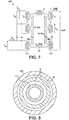
- FIG. 7 is a circuit diagram of a seventh embodiment of a transformer according to the invention.
- FIG. 8 is a schematic end view of transformer cores and windings of a first embodiment of a transformer having the circuit diagram of FIG. 7 ;
- FIG. 9 is a schematic plan and end view of an eighth embodiment of the invention with a plot of voltage along the secondary windings
- FIG. 10 is a schematic plan and end view of a ninth embodiment of the invention with a plot of voltage along the secondary windings;
- FIG. 11 is a schematic plan and end view of a tenth embodiment of the invention with a plot of voltage along the secondary windings;
- FIG. 12 is a schematic plan and end view of an eleventh embodiment of the invention with a plot of voltage along the secondary windings;
- FIG. 13 is a schematic plan and end view of a second embodiment of a transformer having the circuit diagram of FIG. 7 , with a plot of voltage along the secondary windings;
- FIG. 14 is a schematic plan and end view of a twelfth embodiment of the invention with a plot of voltage along the secondary windings;
- FIG. 15 is a photograph of a test example of a partially assembled transformer according to the invention.
- FIG. 16 is a photograph of the test example of FIG. 15 fully assembled.
- Transformers have a primary winding and a secondary winding.
- the primary winding 11 comprises a first plurality Npc of magnetic circuits 111 connected in parallel each with an identical number of turns n pc .
- the secondary winding 12 comprises a second plurality Nsc of magnetic circuits 121 , which need not be the same number as Npc which are connected in series, each of which has a number of turns n sc .
- All the primary and secondary magnetic circuits 111 , 121 are linked by a single turn low resistance loop 13 which electromagnetically couples them together.
- the compound assembly 101 has the following relationships between the primary and secondary voltages and currents.
- Vload is a total voltage across the Nsc secondary turnings 12 and V sc is a voltage across each secondary turning 12 and
- Vloop is a voltage across the single turn low resistance loop 13
- V pri is a voltage across each of the primary turnings 111 in parallel therefore substituting for V sc
- Iloop is a current in the single turn low resistance loop 13
- load is a current in the secondary windings 121
- I pc is a current in each of the primary windings 111 .
- I pri Npc ⁇ I pc where I pri is a sum of the currents in the Npc primary turnings 111 therefore, substituting for I pc
- Vload V pri I pri Iload
- the ratios are independent of a number Nsc of secondary windings or cores 121 .
- Other known transformer rules apply such as impedance transformations and shunt inductances as they would for any transformer.
- circuit diagram of FIG. 1 a represents a transformer with a number of multiple magnetic circuits.
- a transformer 102 is illustrated similar to the transformer 101 illustrated in FIG. 1 a , but in which each of the Nsc secondary windings 121 is provided with a respective Br 1-n , rectifier 24 and a C 1-n , filter 23 respectively, so that the transformer 102 output is rectified to provide a DC output.
- an advantage of the multiple core 121 transformer described is that the transformer ideally lends itself to a multiple rectifier 24 approach.
- a risk of failure of components must be considered.
- a short circuit failure shorts out only a single core thus the system can continue to operate with the remaining cores until a suitable service interval for shut down and repair is reached. This is a very valuable characteristic in regard to reliability.
- rectifier failure of a single rectifier can shut down an entire system.
- FIG. 1 c shows a circuit diagram of a transformer 103 according to a third embodiment of the invention using L 1-N inductive smoothing filters 25 in an output circuit of each of the secondary coils 121 , which adaptation is well known in the art.
- FIG. 1 d shows a circuit diagram of a fourth embodiment 104 with L 1-N double wound inductors 26 in place of the inductive smoothing filters 25 , which further aid in reduction of stray capacitance effects described earlier herein, as portions of the individual choke structures 26 have DC voltages between the windings and not alternating voltage.
- FIG. 1 e a circuit diagram of a fifth embodiment 105 is illustrated which uses a common magnetic core 27 through all of the inductive smoothing filter single wound windings 28 similar to those of the third embodiment, and this is further discussed later herein in relation to assembly techniques.
- FIG. 1 f a circuit diagram of a sixth embodiment 106 is illustrated which uses a common magnetic core 27 through all of the inductive smoothing filter double wound windings 29 similar to those of the fourth embodiment.
- FIG. 1 g is a circuit diagram of a seventh embodiment 107 in which instead of connecting all the primaries 111 in parallel each primary winding is powered by a respective power supply 29 , psu 1 to psuN.
- Each power supply unit 29 is suitably designed so that the power supply units behaves as a relatively low impedance to the loop and the remaining power supplies make up a required power input, so that overall performance of the system is not adversely affected if one power supply unit fails.
- a spare power supply unit 29 is installed in the system and powered up only when one of the other power supply units fails.
- All the power supply units are operated with a symmetrical AC output with a suitable phase to add, operate with a common output current, and are synchronised. Small voltage variations in V pc between each of the power supply units modules can be tolerated and the total voltage V loop is the sum of all the individuals V pc outputs.
- the power supply units all operate in parallel from a DC link with all positive poles connected in parallel and all negative poles in parallel.
- FIGS. 2 a and 2 b A realisation of the circuit diagram shown in FIG. 1 b of the second embodiment 102 of the invention is shown in FIGS. 2 a and 2 b , in which primary toroids 111 at low voltage are located coaxially with, and at least partially within, secondary toroids 121 operated at high voltage, as illustrated in Example 1 herein.
- a key advantage of this system is that voltage insulation requirements are between structures that have large diameters and reasonably smooth surfaces. This is ideal because as voltages rise it is important to avoid sharp points that cause significantly sharp field enhancements that can lead to failure by voltage breakdown.
- Epk is a peak electric field
- Sizes of the toroidal cores 111 , 121 are preferably selected such that a required winding for both the primary cores 111 and secondary cores 121 can be achieved with a single layer winding. This is most desirable but is not essential and multi-layer windings could be used.
- An advantage of a single layer winding is that eddy current losses in the wires are minimised as layers can otherwise compound eddy current loss to a very high degree. Also as a voltage on an individual core is low, the winding can be placed directly on a plastic finish that is usually found on the toroid core. The apparatus requires no further complex insulation systems between the core and the winding. Also with a single layer winding the actual winding operation of putting a single layer winding on a toroid is one of the simplest and lowest cost processes in transformer winding.
- a choice of materials for the core, an operating frequency, and individual core dimensions are determined by calculations for each individual core based upon load, and Vloop. In this regard standard methods of calculation, assuming each individual toroid has a single turn winding, are applied. It may be expected that the benefits of the apparatus will be relevant when the core material is ferrite or nanocrystalline material.
- assembly 102 with five individual secondary toroids 121 as an example but another number, even as many as 30 or 40 toroids could be used.
- Each secondary coil 121 is mounted on a printed circuit board 3 on which the Brn rectifiers 24 and the CN filter capacitors 23 are also mounted.
- a radial space 8 between the primary coils 111 and the secondary coils 121 is shown in the end view of FIG. 2 b and can be designed for a required voltage hold off as detailed earlier herein.
- the loop 13 that links all the cores is formed by a central conductive tube 4 passing axially through the primary and secondary coils and by formed conductive end cheeks and base 5 .
- the system can be immersed in a fluid for cooling and for voltage hold off enhancement requirements by known methods.
- the use of a thin walled tube 4 and a flat structure with a high surface area for the end cheeks and base is most appropriate.
- multiple small tubes and/or a slot down the length of the tube may also improve current distribution and lower AC resistance of the tube, which is desirable.
- Apertures 29 may be located in the end cheek 5 so that, as shown in FIG. 2 a , fluid flow 9 can be directed thorough the assembly if required for cooling the transformer.
- FIGS. 4 a and 4 b show a system 103 where the PCBs 3 have added the LN inductors 25 shown in FIGS. 1 c and 1 d.
- FIGS. 5 a and 5 b show the embodiments 105 , 106 of the invention employing the circuits of FIGS. 1 e and 1 f in which the coils 111 , 121 are wound not as toroids but in a conventional form. Then a suitably insulated core, which may be made from an assembly of toroids, one inside the other, may be used as a common magnetic circuit. By placing toroids one inside the other a very large area magnetic circuit can be produced which is ideal for a high current filter application. This type of magnetic circuit is best used with ferrite or iron powder cores that use a particulate form of magnetic material rather than strip wound cores. A photograph of components of the embodiments 105 , 106 is shown in FIG. 6 .
- the core 61 shown in the centre of the photograph and the right-hand core 62 each show a wire (winding) 611 , 621 respectively passing through the toroid—this is a normal way of using such a core.
- a wire (winding) 611 , 621 By placing a group of the smaller cores 62 inside a group of the larger cores 61 a long magnetic core 63 of large area can be made.
- the wire (winding) 631 passes around an outer diameter of the outer core 61 .
- This arrangement has a large air gap and thus a low ⁇ —most desirable for a DC power supply filter choke.
- FIG. 7 shows a circuit diagram of a seventh embodiment 107 of the invention with a deliberate introduction of an inductance 71 in the loop as L_Loop. Voltages in the loop across the primary Vp_Loop and the secondary Vs_loop that were virtually identical in the basic design are now therefore different and calculations are made by using different values of V_Loop for the primary and secondary coils 111 , 121 .
- realisation of L_Loop 71 can be made in a transformer in which the primary and secondary windings are coaxial by inserting magnetic material 81 in a cylindrical space 8 between the primary and secondary coils 111 , 121 .
- the insulation spaces 8 must be rated for the voltage hold off required or the magnetic material 81 may be of a type of ferrite that has high hold off voltage capabilities.
- Certain nickel zinc ferrites can reliably hold off voltage up to 2 kV/mm and so a transformer with leakage inductance using the magnetic material as both the high voltage insulator and the magnetic core can be made.
- the coils 111 , 121 do not have to be coaxial but may be side by side as shown in an eighth embodiment 108 of the invention.
- a linear gradient over the coils will result in the high voltage at one end so that an eht insulator 91 is required. This increases the loop length.
- the primary coils 111 in this and following descriptions the term “coil” implies a toroid with a winding, have a same diameter; with an eht system the primary coils need less voltage clearance than otherwise.
- two groups of secondary coils 121 may be used by arranging the groups so that a high voltage is in a centre of the two groups as shown in the accompanying graph.
- the high voltage point can be brought out at the centre. This significantly simplifies the eht insulation design and results in a smaller, i.e. shorter, secondary system than in the previous embodiment 108 .
- the parallel secondary coils 121 also increase current capability.
- the primary loop tube 4 may have a larger diameter than in previously described embodiments to reduce copper loss if required.
- an apparatus realising the coupling loop 13 may have a design with a linear conductor with the return path formed by a wider, possibly grounded, strip 131 .
- Supporting primary side power electronics may be mounted on an opposite side of the strip from the windings. Water (or air) cooling this strip allows it to form a central mechanical interface for a power electronics system of the converter.
- the embodiment 110 of FIG. 11 can be adapted to arrangements like that of the eighth embodiment 108 of FIG. 9 .
- a wider strip 132 may help reduce resistance slightly, but requires more joins. Connection methods are important with the primary structure and as power/frequency contours rise this may become a weak link. However it now becomes possible to fit a screen 122 between the primary and secondary coil systems 111 , 121 .
- the circuit shown in FIG. 7 can alternatively be realised by fitting cores 71 on the primary loop, which fit inside the primary coils 111 .
- This produces a same equivalent circuit as in FIG. 7 but would not increase loop length.
- the relatively low inductance at the loop level could, in a wide number of circumstances, be achieved by the use of low Ur cores slipped over a part of the loop.
- any of the preceding embodiments can be adapted to use an arrangement where the secondary coils 121 increase in diameter as the voltage gradient increases, or reduce as the voltage gradient decreases.
- core loss could be reduced such an embodiment would require manufacture of a larger number of different size coils.
- the secondary coils 121 may be directly connected in series or each one may have a rectifier system, as with the coaxial embodiments.
- This rectifier system may be a bridge or voltage multiplying arrangement if so desired.
- the loop 13 may be formed from a number of smaller tubes so that a surface area of the loop is increased thus desirably reducing AC resistance effects.
- the primary coils 111 can be arranged in series and/or parallel groupings as required.
- a convenient concept is to put all the primary coils in parallel and use the same winding as the secondary coils—thus reducing parts variance and increasing the quantities of the coils of a same type which are manufactured by a factor of two.
- a secondary side smoothing inductor may also be employed. Some embodiments require, and some embodiments may benefit from, this inductor.
- the inductor is normally referred to as a choke input filter. If such an arrangement is required then the arrangement can be readily adapted into the approach described herein.
- Each secondary coil and rectifier would have an associated smaller inductor system, these circuit elements would be series connected.
- a transformer was constructed with two magnetic circuits mounted coaxially one inside the other.
- An outer core TX87/54/14 was wound with 73 turns of ptfe covered 19/0.2 mm silver plated copper wire.
- the inner core was TN36/23/15 wound with 34 turns of the same wire.
- the system was interconnected with a fabricated single turn structure using 1 oz/ft 2 copper clad board and 50 ⁇ M copper.
- the photographs of FIGS. 15 and 16 indicate the assembly technique.
- FIG. 15 shows a location of the cores before final fitting of the single turn coupling system.
- FIG. 16 shows the final assembly. The unit was tested using low level RF bridges.
- the ratio based on square root of the inductance ratio is 2.104, the value based upon the turns is 2.147 which is well within measurement error.
- the leakage inductance was checked on one coil with the other coil terminals shorted.
Abstract
Description
Vload=Nsc·V sc
where Vload is a total voltage across the Nsc
and
where Vloop is a voltage across the single turn
therefore substituting for Vsc
For the Current Ratio from Secondary to Primary
Iloop=n sc ·Iload=n pc ·I pc
where Iloop is a current in the single turn
and
I pri =Npc·I pc
where Ipri is a sum of the currents in the Npc
Thus, it can be seen that, as would be expected from a known transformer:
| Frequency | Ls Outer Coil Rs | Ls |
||
| 10 kHz | 50.17 μH | 4.68 R | 10.7 μH | 1.06 R |
Claims (22)
Applications Claiming Priority (3)
| Application Number | Priority Date | Filing Date | Title |
|---|---|---|---|
| GB0706197.1 | 2007-03-29 | ||
| GB0706197A GB2447963B (en) | 2007-03-29 | 2007-03-29 | High frequency transformer for high voltage applications |
| PCT/GB2008/000980 WO2008119935A1 (en) | 2007-03-29 | 2008-03-19 | High frequency transformer for high voltage applications |
Publications (2)
| Publication Number | Publication Date |
|---|---|
| US20100231341A1 US20100231341A1 (en) | 2010-09-16 |
| US8324999B2 true US8324999B2 (en) | 2012-12-04 |
Family
ID=38050510
Family Applications (1)
| Application Number | Title | Priority Date | Filing Date |
|---|---|---|---|
| US12/593,136 Expired - Fee Related US8324999B2 (en) | 2007-03-29 | 2008-03-19 | High frequency transformer for high voltage applications |
Country Status (7)
| Country | Link |
|---|---|
| US (1) | US8324999B2 (en) |
| EP (1) | EP2156449B1 (en) |
| JP (1) | JP5813320B2 (en) |
| CN (1) | CN101681717B (en) |
| AU (1) | AU2008234707B2 (en) |
| GB (1) | GB2447963B (en) |
| WO (1) | WO2008119935A1 (en) |
Cited By (1)
| Publication number | Priority date | Publication date | Assignee | Title |
|---|---|---|---|---|
| TWI620210B (en) * | 2016-08-22 | 2018-04-01 | 致茂電子股份有限公司 | Transformer embedded with thermally conductive member |
Families Citing this family (11)
| Publication number | Priority date | Publication date | Assignee | Title |
|---|---|---|---|---|
| GB2462291B (en) * | 2008-07-31 | 2012-07-18 | E2V Tech Uk Ltd | Multi-toroid transformer |
| KR101675166B1 (en) * | 2010-11-18 | 2016-11-10 | 두산공작기계 주식회사 | Transformer having a function of common-mode noise rejection |
| JP2013131589A (en) * | 2011-12-21 | 2013-07-04 | Mitsubishi Electric Corp | Winding for transformer, transformer, and power converter |
| CN103023359A (en) * | 2012-12-31 | 2013-04-03 | 江苏一同环保工程技术有限公司 | High-power high-frequency high-voltage series-connection superposition power supply |
| CN103391078A (en) * | 2013-07-19 | 2013-11-13 | 中国电子科技集团公司第十四研究所 | Small and efficient high-power solid-state modulator |
| FR3015146B1 (en) * | 2013-12-16 | 2018-04-06 | Ge Energy Power Conversion Technology Limited | SYSTEMS AND METHODS FOR PROVIDING AUXILIARY CURRENT SUPPLY IN HIGH VOLTAGE CONVERTERS |
| KR101611560B1 (en) | 2014-11-11 | 2016-04-11 | 김남조 | Direct Current Transformer, and conduction heating apparatus using DC transformer |
| US10951123B2 (en) | 2015-04-23 | 2021-03-16 | Chicony Power Technology Co.. Ltd. | Power conversion system |
| US9559609B2 (en) | 2015-04-23 | 2017-01-31 | Chicony Power Technology Co., Ltd. | Integrated power-converting module |
| FR3045925B1 (en) * | 2015-12-22 | 2018-02-16 | Supergrid Institute | ELECTRICAL TRANSFORMER FOR REMOTE HIGH VOLTAGE EQUIPMENT |
| CN106024347B (en) * | 2016-07-03 | 2018-01-02 | 衢州昀睿工业设计有限公司 | The extra-high voltage generating means of multiple transformers combination |
Citations (40)
| Publication number | Priority date | Publication date | Assignee | Title |
|---|---|---|---|---|
| GB427948A (en) | 1933-11-02 | 1935-05-02 | British Thomson Houston Co Ltd | Improvements in and relating to electric transformers |
| US2600057A (en) * | 1949-05-18 | 1952-06-10 | Quentin A Kerns | High-voltage multiple core transformer |
| US2792547A (en) * | 1954-11-12 | 1957-05-14 | Westinghouse Electric Corp | Magnetic amplifier for control purposes |
| US3016342A (en) * | 1957-08-29 | 1962-01-09 | Kruskal Martin | Controlled nuclear fusion reactor |
| US3195038A (en) * | 1961-05-15 | 1965-07-13 | Brentford Electric Ltd | Voltage or current regulator apparatus |
| US3363165A (en) * | 1965-05-20 | 1968-01-09 | Power Conversion Inc | Transformer with plurality of secondary windings and low a.c. potential therebetween |
| US3368137A (en) * | 1963-05-17 | 1968-02-06 | Westinghouse Brake & Signal | High current intensity rectifiers using bar-type conductors |
| US3437965A (en) * | 1963-12-27 | 1969-04-08 | Ogallala Electronics Mfg Inc | Heat exchange apparatus for cooling electromagnetic devices |
| US3440384A (en) * | 1962-11-30 | 1969-04-22 | Charles F Schroeder | Electromagnetic unit |
| US3568035A (en) | 1968-03-20 | 1971-03-02 | Commissariat Energie Atomique | Device for the production of a high direct voltage difference |
| US3745440A (en) | 1972-02-28 | 1973-07-10 | Litton Systems Inc | Electrical inverter-rectifier circuit and inductor apparatus therefor |
| US3919595A (en) * | 1972-09-01 | 1975-11-11 | Gen Electric | Lamp ballast device |
| US4016477A (en) * | 1975-04-29 | 1977-04-05 | Isodyne Inc. | Novel multi-path leakage transformer and inverter ballast |
| US4339704A (en) * | 1980-07-07 | 1982-07-13 | General Electric Company | Series parallel transition for power supply |
| US4739296A (en) * | 1985-12-16 | 1988-04-19 | Mitsubishi Denki Kabushiki Kaisha | Current transformer cooled by a circulating dielectric fluid |
| JPS6388811A (en) | 1986-10-02 | 1988-04-19 | Matsushita Electric Ind Co Ltd | Fly-back transformer device |
| US4779035A (en) | 1986-09-02 | 1988-10-18 | Electro-Voice, Incorporated | End of charge detector |
| US4956626A (en) * | 1989-01-13 | 1990-09-11 | Sundstrand Corporation | Inductor transformer cooling apparatus |
| US5023768A (en) * | 1989-11-24 | 1991-06-11 | Varian Associates, Inc. | High voltage high power DC power supply |
| US5166965A (en) * | 1991-04-11 | 1992-11-24 | Varian Associates, Inc. | High voltage dc source including magnetic flux pole and multiple stacked ac to dc converter stages with planar coils |
| JPH05243060A (en) | 1992-03-02 | 1993-09-21 | Nippon Telegr & Teleph Corp <Ntt> | Chalk and transformer for switching power supply |
| JPH11176678A (en) | 1997-11-14 | 1999-07-02 | Ind Technol Res Inst | Module series type of high-voltage transformer |
| JP2000260640A (en) | 1999-03-12 | 2000-09-22 | Cosel Co Ltd | Output transformer |
| JP2001068359A (en) | 1999-08-31 | 2001-03-16 | Agilent Technologies Japan Ltd | Transformer device |
| US6255783B1 (en) * | 1998-03-17 | 2001-07-03 | Ventex Group Llc | Gas discharge lamp power supply with feed forward compensation for input voltage variations |
| JP2002083718A (en) | 2000-09-11 | 2002-03-22 | Daihen Corp | Stationary induction electrical apparatus |
| DE10100829C1 (en) | 2001-01-10 | 2002-05-08 | Rainer Menge | Induction annealing device used for conductively heating a wire comprises transformers with parallel primary windings each wound around a magnetic core formed by a packet of annular cores made of highly permeable material |
| US6788184B2 (en) * | 2000-07-21 | 2004-09-07 | Michel Roche | High frequency transformer with integrated rectifiers |
| US6909352B2 (en) * | 1998-11-13 | 2005-06-21 | Merlex Corporation Pty Ltd. | Endless core for a multiphase transformer and a transformer incorporating same |
| JP2006013094A (en) | 2004-06-25 | 2006-01-12 | Densei Lambda Kk | Transformer structure |
| US7009853B2 (en) * | 2002-04-25 | 2006-03-07 | Abb Patent Gmbh | Switched-mode power supply arrangement |
| US7015784B2 (en) * | 2003-01-21 | 2006-03-21 | Kazuo Kohno | Wound-rotor transformer and power source device using said wound-rotor transformer |
| US7042323B2 (en) * | 2002-08-22 | 2006-05-09 | Abb Research Ltd | Signal transformer and method for operating such a signal transformer |
| JP2006147885A (en) | 2004-11-19 | 2006-06-08 | Minebea Co Ltd | High voltage transformer |
| US7294971B2 (en) * | 2003-10-06 | 2007-11-13 | Microsemi Corporation | Balancing transformers for ring balancer |
| US7318270B1 (en) * | 2005-04-14 | 2008-01-15 | United States Of America As Represented By The Secretary Of The Air Force | Method for producing a full wave bridge rectifier suitable for low-voltage, high-current operation |
| US7332992B2 (en) * | 2006-04-07 | 2008-02-19 | Sony Corporation | Transformer |
| US7447048B2 (en) * | 2005-09-02 | 2008-11-04 | Sony Corporation | Switching power supply circuit |
| US7652551B2 (en) * | 2001-01-23 | 2010-01-26 | Buswell Harrie R | Toroidal inductive devices and methods of making the same |
| US7705705B2 (en) * | 2006-01-03 | 2010-04-27 | Delta Electronics Inc. | Transformer structure |
Family Cites Families (8)
| Publication number | Priority date | Publication date | Assignee | Title |
|---|---|---|---|---|
| US4338951A (en) * | 1980-08-19 | 1982-07-13 | Critikon, Inc. | Magnetically coupled isolation interface circuit |
| JPS57206274A (en) * | 1981-06-11 | 1982-12-17 | Matsushita Electric Ind Co Ltd | Flyback transformer |
| JPS6377319U (en) * | 1986-11-07 | 1988-05-23 | ||
| GB9111535D0 (en) * | 1991-05-29 | 1991-07-17 | Measurement Tech Ltd | Improvements in or relating to transformers |
| JP2971220B2 (en) * | 1991-11-13 | 1999-11-02 | 富士電気化学株式会社 | Transformer coil element, transformer using the coil element, and method of connecting the transformer |
| US5952849A (en) * | 1997-02-21 | 1999-09-14 | Analog Devices, Inc. | Logic isolator with high transient immunity |
| JP2001274020A (en) * | 2000-03-23 | 2001-10-05 | Sanyo Electric Co Ltd | Coil unit, coil, transformer, and boosting circuit |
| US7187263B2 (en) * | 2003-11-26 | 2007-03-06 | Vlt, Inc. | Printed circuit transformer |
-
2007
- 2007-03-29 GB GB0706197A patent/GB2447963B/en not_active Expired - Fee Related
-
2008
- 2008-03-19 US US12/593,136 patent/US8324999B2/en not_active Expired - Fee Related
- 2008-03-19 WO PCT/GB2008/000980 patent/WO2008119935A1/en active Application Filing
- 2008-03-19 AU AU2008234707A patent/AU2008234707B2/en not_active Ceased
- 2008-03-19 CN CN2008800177714A patent/CN101681717B/en not_active Expired - Fee Related
- 2008-03-19 JP JP2010500346A patent/JP5813320B2/en not_active Expired - Fee Related
- 2008-03-19 EP EP08718817.3A patent/EP2156449B1/en not_active Not-in-force
Patent Citations (44)
| Publication number | Priority date | Publication date | Assignee | Title |
|---|---|---|---|---|
| GB427948A (en) | 1933-11-02 | 1935-05-02 | British Thomson Houston Co Ltd | Improvements in and relating to electric transformers |
| US2600057A (en) * | 1949-05-18 | 1952-06-10 | Quentin A Kerns | High-voltage multiple core transformer |
| US2792547A (en) * | 1954-11-12 | 1957-05-14 | Westinghouse Electric Corp | Magnetic amplifier for control purposes |
| US3016342A (en) * | 1957-08-29 | 1962-01-09 | Kruskal Martin | Controlled nuclear fusion reactor |
| US3195038A (en) * | 1961-05-15 | 1965-07-13 | Brentford Electric Ltd | Voltage or current regulator apparatus |
| US3440384A (en) * | 1962-11-30 | 1969-04-22 | Charles F Schroeder | Electromagnetic unit |
| US3368137A (en) * | 1963-05-17 | 1968-02-06 | Westinghouse Brake & Signal | High current intensity rectifiers using bar-type conductors |
| US3437965A (en) * | 1963-12-27 | 1969-04-08 | Ogallala Electronics Mfg Inc | Heat exchange apparatus for cooling electromagnetic devices |
| US3363165A (en) * | 1965-05-20 | 1968-01-09 | Power Conversion Inc | Transformer with plurality of secondary windings and low a.c. potential therebetween |
| US3568035A (en) | 1968-03-20 | 1971-03-02 | Commissariat Energie Atomique | Device for the production of a high direct voltage difference |
| US3745440A (en) | 1972-02-28 | 1973-07-10 | Litton Systems Inc | Electrical inverter-rectifier circuit and inductor apparatus therefor |
| US3919595A (en) * | 1972-09-01 | 1975-11-11 | Gen Electric | Lamp ballast device |
| US4016477A (en) * | 1975-04-29 | 1977-04-05 | Isodyne Inc. | Novel multi-path leakage transformer and inverter ballast |
| US4339704A (en) * | 1980-07-07 | 1982-07-13 | General Electric Company | Series parallel transition for power supply |
| US4739296A (en) * | 1985-12-16 | 1988-04-19 | Mitsubishi Denki Kabushiki Kaisha | Current transformer cooled by a circulating dielectric fluid |
| US4779035A (en) | 1986-09-02 | 1988-10-18 | Electro-Voice, Incorporated | End of charge detector |
| JPS6388811A (en) | 1986-10-02 | 1988-04-19 | Matsushita Electric Ind Co Ltd | Fly-back transformer device |
| US4956626A (en) * | 1989-01-13 | 1990-09-11 | Sundstrand Corporation | Inductor transformer cooling apparatus |
| US5023768A (en) * | 1989-11-24 | 1991-06-11 | Varian Associates, Inc. | High voltage high power DC power supply |
| US5166965A (en) * | 1991-04-11 | 1992-11-24 | Varian Associates, Inc. | High voltage dc source including magnetic flux pole and multiple stacked ac to dc converter stages with planar coils |
| JPH05243060A (en) | 1992-03-02 | 1993-09-21 | Nippon Telegr & Teleph Corp <Ntt> | Chalk and transformer for switching power supply |
| JPH11176678A (en) | 1997-11-14 | 1999-07-02 | Ind Technol Res Inst | Module series type of high-voltage transformer |
| US6255783B1 (en) * | 1998-03-17 | 2001-07-03 | Ventex Group Llc | Gas discharge lamp power supply with feed forward compensation for input voltage variations |
| US6909352B2 (en) * | 1998-11-13 | 2005-06-21 | Merlex Corporation Pty Ltd. | Endless core for a multiphase transformer and a transformer incorporating same |
| JP2000260640A (en) | 1999-03-12 | 2000-09-22 | Cosel Co Ltd | Output transformer |
| US6377153B1 (en) | 1999-08-31 | 2002-04-23 | Agilent Technologies, Inc. | Transformer apparatus for use in insulated switching power supply apparatus with reduction of switching noise |
| JP2001068359A (en) | 1999-08-31 | 2001-03-16 | Agilent Technologies Japan Ltd | Transformer device |
| US6788184B2 (en) * | 2000-07-21 | 2004-09-07 | Michel Roche | High frequency transformer with integrated rectifiers |
| JP2002083718A (en) | 2000-09-11 | 2002-03-22 | Daihen Corp | Stationary induction electrical apparatus |
| DE10100829C1 (en) | 2001-01-10 | 2002-05-08 | Rainer Menge | Induction annealing device used for conductively heating a wire comprises transformers with parallel primary windings each wound around a magnetic core formed by a packet of annular cores made of highly permeable material |
| US7652551B2 (en) * | 2001-01-23 | 2010-01-26 | Buswell Harrie R | Toroidal inductive devices and methods of making the same |
| US7009853B2 (en) * | 2002-04-25 | 2006-03-07 | Abb Patent Gmbh | Switched-mode power supply arrangement |
| US7042323B2 (en) * | 2002-08-22 | 2006-05-09 | Abb Research Ltd | Signal transformer and method for operating such a signal transformer |
| US7015784B2 (en) * | 2003-01-21 | 2006-03-21 | Kazuo Kohno | Wound-rotor transformer and power source device using said wound-rotor transformer |
| US7129813B2 (en) * | 2003-01-21 | 2006-10-31 | Kazuo Kohno | Wound-rotor transformer and power source device using said wound-rotor transformer |
| US7294971B2 (en) * | 2003-10-06 | 2007-11-13 | Microsemi Corporation | Balancing transformers for ring balancer |
| JP2006013094A (en) | 2004-06-25 | 2006-01-12 | Densei Lambda Kk | Transformer structure |
| JP2006147885A (en) | 2004-11-19 | 2006-06-08 | Minebea Co Ltd | High voltage transformer |
| EP1814129A1 (en) | 2004-11-19 | 2007-08-01 | Minebea Co., Ltd. | High-voltage transformer |
| US20080024261A1 (en) | 2004-11-19 | 2008-01-31 | Hiroshi Shinmen | High Voltage Transformer |
| US7318270B1 (en) * | 2005-04-14 | 2008-01-15 | United States Of America As Represented By The Secretary Of The Air Force | Method for producing a full wave bridge rectifier suitable for low-voltage, high-current operation |
| US7447048B2 (en) * | 2005-09-02 | 2008-11-04 | Sony Corporation | Switching power supply circuit |
| US7705705B2 (en) * | 2006-01-03 | 2010-04-27 | Delta Electronics Inc. | Transformer structure |
| US7332992B2 (en) * | 2006-04-07 | 2008-02-19 | Sony Corporation | Transformer |
Non-Patent Citations (2)
| Title |
|---|
| International Search Report of PCT/GB2008/000980 dated Jul. 4, 2008. |
| Partial English Translation of a Japanese Office Action dated Jul. 30, 2012, issued in counterpart Patent Application No. 2010-500346. |
Cited By (1)
| Publication number | Priority date | Publication date | Assignee | Title |
|---|---|---|---|---|
| TWI620210B (en) * | 2016-08-22 | 2018-04-01 | 致茂電子股份有限公司 | Transformer embedded with thermally conductive member |
Also Published As
| Publication number | Publication date |
|---|---|
| CN101681717A (en) | 2010-03-24 |
| EP2156449A1 (en) | 2010-02-24 |
| AU2008234707A1 (en) | 2008-10-09 |
| JP2010522979A (en) | 2010-07-08 |
| JP5813320B2 (en) | 2015-11-17 |
| GB2447963A (en) | 2008-10-01 |
| US20100231341A1 (en) | 2010-09-16 |
| GB2447963B (en) | 2011-11-16 |
| AU2008234707B2 (en) | 2012-06-28 |
| GB0706197D0 (en) | 2007-05-09 |
| CN101681717B (en) | 2013-07-10 |
| EP2156449B1 (en) | 2014-05-21 |
| WO2008119935A1 (en) | 2008-10-09 |
Similar Documents
| Publication | Publication Date | Title |
|---|---|---|
| US8324999B2 (en) | High frequency transformer for high voltage applications | |
| CN108364761B (en) | Integrated magnetic assembly and switched mode power converter | |
| US8847719B2 (en) | Transformer with split primary winding | |
| US6429763B1 (en) | Apparatus and method for PCB winding planar magnetic devices | |
| EP0698896B1 (en) | Printed coil | |
| RU2374713C2 (en) | Planar high-voltage transformer | |
| US8779882B2 (en) | Center tapped transformers for isolated power converters | |
| US11031878B2 (en) | Resonant converter and manufacturing method of transformer thereof | |
| US10050533B2 (en) | High voltage high frequency transformer | |
| US7148779B2 (en) | Pulse type transformer with increased coupling coefficient through configuration of plural primary windings | |
| US6664881B1 (en) | Efficient, low leakage inductance, multi-tap, RF transformer and method of making same | |
| US4922156A (en) | Integrated power capacitor and inductors/transformers utilizing insulated amorphous metal ribbon | |
| US9287035B2 (en) | Flyback converter using coaxial cable transformer | |
| CN110970210A (en) | Transformer device | |
| EP0989717A2 (en) | A power feed for a submarine communications system | |
| US9490065B2 (en) | High voltage transformer | |
| US20170040097A1 (en) | Switching converter circuit with an integrated transformer | |
| US11177066B2 (en) | Egg-shaped continuous coils for inductive components | |
| EP3893256A1 (en) | Semi-planar transformer | |
| CN113811963B (en) | Variable device | |
| US11735357B2 (en) | Transformer with improved insulation structure | |
| WO2022064662A1 (en) | Transformer and converter | |
| Waffenschmidt et al. | Planar resonant multi-output transformer for printed circuit board integration | |
| CN116420206A (en) | Transformer unit |
Legal Events
| Date | Code | Title | Description |
|---|---|---|---|
| AS | Assignment |
Owner name: E2V TECHNOLOGIES (UK) LIMITED, UNITED KINGDOM Free format text: ASSIGNMENT OF ASSIGNORS INTEREST;ASSIGNOR:RICHARDSON, ROBERT;REEL/FRAME:023757/0704 Effective date: 20091111 |
|
| FEPP | Fee payment procedure |
Free format text: PAYOR NUMBER ASSIGNED (ORIGINAL EVENT CODE: ASPN); ENTITY STATUS OF PATENT OWNER: LARGE ENTITY |
|
| STCF | Information on status: patent grant |
Free format text: PATENTED CASE |
|
| FPAY | Fee payment |
Year of fee payment: 4 |
|
| AS | Assignment |
Owner name: TELEDYNE E2V (UK) LIMITED, CALIFORNIA Free format text: CHANGE OF NAME;ASSIGNOR:E2V TECHNOLOGIES (UK) LIMITED;REEL/FRAME:043277/0908 Effective date: 20170329 |
|
| AS | Assignment |
Owner name: TELEDYNE UK LIMITED, CALIFORNIA Free format text: CHANGE OF NAME;ASSIGNOR:TELEDYNE E2V (UK) LIMITED;REEL/FRAME:051461/0294 Effective date: 20191230 |
|
| FEPP | Fee payment procedure |
Free format text: MAINTENANCE FEE REMINDER MAILED (ORIGINAL EVENT CODE: REM.); ENTITY STATUS OF PATENT OWNER: LARGE ENTITY |
|
| LAPS | Lapse for failure to pay maintenance fees |
Free format text: PATENT EXPIRED FOR FAILURE TO PAY MAINTENANCE FEES (ORIGINAL EVENT CODE: EXP.); ENTITY STATUS OF PATENT OWNER: LARGE ENTITY |
|
| STCH | Information on status: patent discontinuation |
Free format text: PATENT EXPIRED DUE TO NONPAYMENT OF MAINTENANCE FEES UNDER 37 CFR 1.362 |
|
| FP | Lapsed due to failure to pay maintenance fee |
Effective date: 20201204 |