US8258564B2 - Integrated circuit with floating-gate electrodes including a transition metal and corresponding manufacturing method - Google Patents
Integrated circuit with floating-gate electrodes including a transition metal and corresponding manufacturing method Download PDFInfo
- Publication number
- US8258564B2 US8258564B2 US12/104,750 US10475008A US8258564B2 US 8258564 B2 US8258564 B2 US 8258564B2 US 10475008 A US10475008 A US 10475008A US 8258564 B2 US8258564 B2 US 8258564B2
- Authority
- US
- United States
- Prior art keywords
- floating
- gate electrodes
- transition metal
- integrated circuit
- layer
- Prior art date
- Legal status (The legal status is an assumption and is not a legal conclusion. Google has not performed a legal analysis and makes no representation as to the accuracy of the status listed.)
- Active, expires
Links
Images


Classifications
-
- H—ELECTRICITY
- H10—SEMICONDUCTOR DEVICES; ELECTRIC SOLID-STATE DEVICES NOT OTHERWISE PROVIDED FOR
- H10B—ELECTRONIC MEMORY DEVICES
- H10B41/00—Electrically erasable-and-programmable ROM [EEPROM] devices comprising floating gates
- H10B41/30—Electrically erasable-and-programmable ROM [EEPROM] devices comprising floating gates characterised by the memory core region
Definitions
- the invention generally relates to an integrated circuit. Furthermore, the invention also relates to a corresponding manufacturing method for an integrated circuit.
- Floating gate transistors are commonly used for non-volatile storage such as NAND flash devices and NOR flash devices to store the charge of one or more bits per floating gate transistor in the associated floating gate.
- the floating gate is mounted above an active area of substrate silicon which forms the transistor channel and is separated from the substrate by a tunnel dielectric.
- the integrated circuit may include a multitude of floating-gate electrodes, wherein at least one of the floating-gate electrodes has a lower width and an upper width, the lower width being larger than the upper width, and wherein the at least one of the floating-gate electrodes comprises a transition metal.
- the manufacturing method may include: depositing an insulation layer on a semiconductor substrate; depositing at least one layer of floating-gate electrode material on the insulation layer, the at least one layer of floating-gate electrode material comprising a transition metal; forming a multitude of floating-gate electrodes of the at least one layer of floating-gate electrode material, wherein at least one the floating-gate electrodes has a lower width and an upper width, the lower width being larger than the upper width.
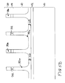
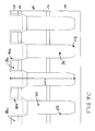
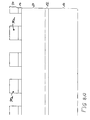
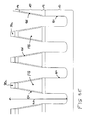
- FIGS. 1A-1E show cross sections of a semiconductor structure for illustrating a manufacturing method for an integrated circuit
- FIGS. 2A-2D show cross sections of another semiconductor structure for illustrating another approach of the manufacturing method
- FIGS. 3A , 3 Ba, 3 Bb and 3 C show cross sections of another semiconductor structure for illustrating another approach of the manufacturing method
- FIGS. 4A and B show cross sections of another semiconductor structure for illustrating another approach of the manufacturing method
- FIGS. 5A-5C show cross sections of another semiconductor structure for illustrating another approach of the manufacturing method
- FIGS. 6A , 6 Ba and 6 Bb show cross sections of another semiconductor structure for illustrating another approach of the manufacturing method
- FIGS. 7A-7F show cross sections of another semiconductor structure for illustrating another approach of the manufacturing method
- FIGS. 8A-8F show cross sections of another semiconductor structure for illustrating another approach of the manufacturing method.
- FIGS. 1A-1E show cross sections of a semiconductor structure for illustrating a manufacturing method for an integrated circuit.
- a method of producing a multilayer semiconductor structure is carried out.
- an insulation layer 12 for example a silicon oxide layer is formed on a surface of a semiconductor substrate 10 .
- the semiconductor substrate 10 includes silicon
- the silicon oxide layer may be formed for instance during a thermal oxidation step.
- the pre-sent technology is not restricted to silicon oxide to provide the insulation layer 12 .
- Various other insulating materials may also be deposited on the semiconductor substrate 10 to provide the insulation layer 12 .
- the layer thickness of the insulation layer 12 may be about 10 nm.
- a layer of a conductive material 14 is deposited on the insulation layer 12 .
- the layer thickness of the layer of a conductive material 14 may be in a range between 10 nm to 30 nm.
- the layer of a conductive material 14 may comprise polysilicon, a metal, a transition metal or a transition metal compound. In the present example, the layer of a conductive material 14 includes polysilicon.
- a transition metal layer 16 is deposited on the layer of a conductive material 14 .
- the transition metal layer 16 may include iridium, ruthenium, a transition metal oxide, a transition metal silicide, a transition metal boride, a transition metal aluminide, a transition metal carbide and/or a transition metal nitride.
- the transition metal layer 16 may include iridium oxide, ruthenium oxide, tungsten silicide, molybdenum silicide, tantalum silicide, titanium silicide, cobalt silicide, zirconium silicide, hafnium silicide, niobium silicide, tungsten nitride, titanium nitride, tantalum nitride, hafnium nitride and/or zirconium nitride.
- the transition metal layer 16 may include at least two of the materials listed above.
- the transition metal layer 16 may have a layer thickness between 20 nm to 100 nm.
- the transition metal of transition metal layer 16 may have a different etch rate than the material of the layer of a conductive material 14 .
- the layer of a conductive material 14 and/or transition metal layer 16 are formed for instance by a chemical vapour deposition (CVD) or by a physical vapour deposition (PVD).
- CVD chemical vapour deposition
- PVD physical vapour deposition
- the materials of the layers 14 and 16 may react with each other.
- the interface between the layers 14 and 16 may not be flat. Instead, the interface between the layers 14 and 16 may have peaks and/or trenches.
- the present technology in not restricted to a non-flat interface between the layers 14 and 16 .
- An oxide layer 18 and a nitride layer 20 are formed on the transition metal layer 16 .
- the semiconductor structure produced by the PMSS-method is shown in FIG. 1A .
- FIG. 1B shows the result of a method of etching trenches (ET-method) into the semiconductor structure of FIG. 1A .
- the ET-method starts with the process step of depositing a (not shown) first mask on the surface of the semiconductor structure.
- the first mask is for instance a carbon hard mask.
- the mask is structured to expose those areas of nitride layer 20 that cover the sites of (later etched) trenches 22 a . This may be done for example by a lithographic step.
- a reactive ion etch (RIE) step is carried out to etch trenches 22 a into the semiconductor structure.
- the RIE step is stopped when the bottoms of the trenches 22 a are within a distance s 1 from the interface of the layers 14 and 16 .
- the distance s 1 may be in a range between 5 nm to 20 nm.
- the ET-method ends.
- An isotropic etch step is carried out to increase the width of the trenches 22 a .
- This isotropic etch step is performed with an etching material that etches the exposed material of the transition metal layer 16 and the oxide layer 18 .
- the nitride of layer 20 is not sensitive against the etching material.
- the first mask is kept on the nitride layer 20 during the isotropic etch step. After the isotropic etch step, the first mask may be removed.
- the newly formed trenches 22 b are shown in FIG. 1C .
- a method of forming nitride spacers (FNS-method) to cover the sidewalls of the trenches 22 b is carried out.
- the trenches 22 b are filled with nitride.
- a second (not shown) mask is deposited on the nitride layer 20 and structured.
- an anisotropic etch step is performed to remove the nitride partially from the trenches 22 b .
- This anisotropic etch step is continued till the bottoms of the trenches 22 b are exposed.
- the anisotropy of this etch step the nitride covering the sidewalls of the trenches 22 b is not attacked more than tolerable.
- the nitride spacers 24 shown in FIG. 1C are formed.
- a second RIE step is carried out to increase the depth of the trenches 22 b .
- the nitride spacers 24 covering the sidewalls of the trenches 22 b are not sensitive against this second RIE step. Therefore, the sidewalls of the trenches 22 b , which are protected by the nitride spacers 24 , are not damaged by this second RIE step.
- the second mask is removed after the second RIE step.
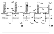
- the result of this second RIE step are trenches 22 c , which extend from the surface of the semiconductor structure into the semiconductor substrate 10 , as can be seen from FIG. 1D .
- the depths of the trenches 22 c is in a range between 100 nm to 300 nm.
- the trenches 22 c have a lower width d 2 which is significantly smaller than the upper width d 1 .
- the lower width d 2 is in a range between 50 nm to 100 nm while the upper width d 1 is in a range between 100 nm to 200 nm.
- Each of these floating-gate electrodes FG includes a lower part 26 formed of the layer of a conductive material 14 and an upper part 28 formed of the transition metal layer 16 .
- the lower part 26 has a column-like shape.
- the upper part 28 has an inverse T-shape, because its width decreases in the direction to the oxide layer 18 .
- Upper width d 3 of the upper part 28 may be in a range between 10 m to 30 nm.
- Lower width d 4 of the upper part 28 which is also the width of the lower part 26 , may be in a range between 50 nm to 100 nm.
- a floating-gate electrode FG with an inverse-T shape or a triangular shape may provide a reduced interaction, i.e. electrical coupling, between the floating-gate electrode FG and an adjacent floating-gate electrode FG associated with another wordline WL.
- the interaction between the floating-gate electrode FG and its associated control-gate electrode CG may not be limited due to the inverse-T shape of the floating-gate electrode FG.
- the upper part 28 of each of the floating-gate electrodes FG includes a transition metal.
- the low resistivity of the transition metal decreases the risk of depletion.
- the lower part 26 of each of the floating-gate electrodes FG includes polysilicon.
- the trenches 22 c are filled with a STI-fill 30 according to the following STI-method.
- the STI-fill-material is deposited on the semiconductor structure.
- a chemical mechanical polishing (CMP) step is carried out to remove those parts of the STI-fill-material that protrude above the nitride spacers 24 .
- the STI-fill 30 is etched back to a level that is within the distance s 1 from the interface of the lower part 26 and the upper part 28 .
- the nitride layer 20 and the nitride spacers 24 are completely removed.
- the oxide layer 18 is not sensitive against hot phosphoric acid.
- oxide spacers 32 are left on the floating-gate electrodes FG, as can be seen from FIG. 1D .
- FCW-method A method of forming control-gate CG electrodes and wordlines WL (FCW-method) on the semiconductor structure of FIG. 1D is performed.
- a layer of coupling dielectric material 34 for instance an oxide, is deposited on the surface of the semiconductor structure.
- a layer of control-gate material 36 for example polysilicon, is deposited on the layer of coupling dielectric material 34 to form control-gate electrodes CG.
- the material of the wordlines WL is deposited on the layer of control gate material 36 .
- the wordlines WL include a tungsten nitride layer 38 and a tungsten layer 40 .
- the oxide spacers 32 are arranged on the top of the floating-gate electrodes FG. Due to the small upper width d 3 of the floating-gate electrodes FG, a relative strong electrical field may occur at the peak-like upper end of each of the floating-gate electrodes FG. To provide an additional insulation on the peak-like upper end of each of the floating-gate electrodes FG is a good way with regard to the strong electrical field.
- the floating-gate electrodes FG may be formed only of the transition metal layer 16 .
- no layer of a conductive material 14 is deposited on the insulation layer 12 and the transition metal layer 16 may have a layer thickness which is in a range between 50 nm to 100 nm.
- the layer of a conductive material 14 may include TaN and the transition metal layer 16 may include tungsten.
- floating-gate electrodes FG are provided that have a lower subunit of TaN and an upper subunit of tungsten.
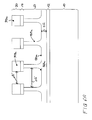
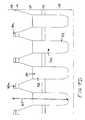
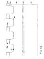
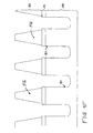
- FIGS. 2A-2D show cross sections of another semiconductor structure for illustrating another approach of the manufacturing method.
- the PMSS-method is carried out to produce the semiconductor structure shown in FIG. 2A .
- the semiconductor structure has a semiconductor substrate 10 , an insulation layer 12 , a transition metal layer 50 and a nitride layer 20 .
- the transition metal layer 50 may include at least one of the materials iridium and/or ruthenium.
- the transition metal layer 50 may also include a transition metal oxide, a transition metal silicide, a transition metal boride, a transition metal aluminide, a transition metal carbide and/or a transition metal nitride.
- the transition metal layer 50 may include at least one of the materials: iridium oxide, ruthenium oxide, tungsten silicide, molybdenum silicide, tantalum silicide, titanium silicide, cobalt silicide, zirconium silicide, hafnium silicide, niobium silicide, tungsten nitride, titanium nitride, tantalum nitride, hafnium nitride and/or zirconium nitride.
- the transition metal layer 50 may have a layer thickness between 50 nm to 100 nm. The variety of the materials suited for the insulation layer 12 is mentioned above.
- the ET-method is performed to etch trenches 52 into the semiconductor structure of FIG. 2A .
- the ET-method is stopped when the newly etched trenches 52 extend from the surface of the semiconductor structure into the semiconductor substrate 10 .
- the total height h 1 of the trenches 52 is in a range between 250 to 350 nm.
- the trenches 52 are filled with an STI-fill 30 according to the STI-method.
- the surface of the STI-fill 30 is within a distance s 2 from the interface between the insulation layer 12 and the transition metal layer 50 , as can be seen from FIG. 2B .
- the distance s 2 may be in a range between 10 nm to 30 nm.
- Nitride layer 20 is removed by an etching step with hot phosphoric acid.
- an isotropic etch step is carried out to form floating-gate electrodes FG of the transition metal layer 50 .
- this isotropic etch step is performed with an etching material which does not attack the STI-fill 30 .
- the result of the isotropic etch step is shown in FIG. 2C .
- the newly formed floating-gate electrodes FG have an inverse-T shape with an upper width d 3 between 10 nm to 50 nm and a lower width d 4 between 30 nm to 100 nm.
- the STI-fill 30 protruding above the interspaces between the floating-gate electrodes FG is etched away. Then, the FCW-method is repeated to form control-gate electrodes CG and wordlines WL. Thus, the semiconductor structure shown in FIG. 2D is produced.
- floating-gate electrodes FG may be formed from two layers of different materials.
- the lower layer may be a polysilicon layer and the upper layer may be a transition metal layer.
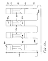
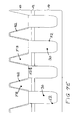
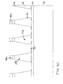
- FIGS. 3A , 3 Ba, 3 Bb and 3 C show cross sections of another semiconductor structure for illustrating another approach of the manufacturing method.
- the PMSS-method is carried out to form a semiconductor structure comprising a semiconductor substrate 10 , an insulation layer 12 , a layer of floating-gate electrode material 60 , an oxide layer 18 and a nitride layer 20 .
- the layer of floating-gate electrode material 60 may include polysilicon and/or at least one transition metal.
- the layer of floating-gate electrode material 60 may include iridium, ruthenium, a transition metal oxide, a transition metal silicide and/or a transition metal nitride.
- the layer of floating-gate electrode material 60 may include a first layer of polysilicon and at least one second layer of a transition metal.
- the ET-method is performed to etch trenches 52 .
- the total height h 1 of these trenches 52 may be in a range between 250 nm to 350 nm.
- the trenches 52 are filled with a STI-fill 30 according to the STI-method.
- the STI-fills 30 have a surface within a distance s 2 from the interface of the insulation layer 12 and the layer of floating-gate electrode material 60 . The result is shown in FIG. 3A .
- strings 62 of the material of former layer of floating-gate electrode material 60 are formed in the interspaces of the trenches 52 .
- the lower parts of the sidewalls of these strings 62 are covered by the STI-fill 30 .
- the upper parts of the sidewalls of the strings 62 are exposed.
- the semiconductor structure of FIG. 3A is heated in an oxygen atmosphere to perform a thermal oxidation of the exposed surfaces of the strings 62 .
- silicon oxide layers 64 are formed that cover the exposed areas of the strings 62 completely.
- These silicon oxide layers 64 may have a layer thickness up to 30 nm.
- the lower parts of the sidewalls of the strings 62 are protected by the STI-fill 30 against the oxygen atmosphere. Therefore, the lower parts of the sidewalls are not oxidised (i.e. the oxidation rate is negligibly small) during the thermal oxidation, as can be seen from FIG. 3 Ba.
- the silicon oxide layers 64 are etched away.
- floating-gate electrodes FG are formed that have an upper width d 3 that is significantly smaller than the lower width d 4 .
- oxide layer 18 and nitride layer 20 are etched away, for instance with hot phosphoric acid and hydrofluoric acid. Then, the FCW-method is performed to form control-gate electrodes CG and wordlines WL. The result is shown in FIG. 3C .
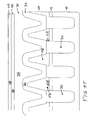
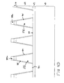
- FIGS. 4A and B show cross sections of another semiconductor structure for illustrating another approach of the manufacturing method.
- a semiconductor structure comprising a semiconductor substrate 10 , an insulation layer 12 , a layer of floating-gate electrode material 60 , an oxide layer 18 and a nitride layer 20 is produced.
- the layer of floating-gate electrode material 60 may include polysilicon and/or at least one transition metal.
- the layer of floating-gate electrode material 60 may include iridium, ruthenium, a transition metal oxide, a transition metal silicide, a transition metal boride, a transition metal aluminide, a transition metal carbide and/or a transition metal nitride.
- the layer of floating-gate electrode material 60 may include at least two layers of different materials.
- the ET-method is repeated.
- the newly etched trenches 52 extend from the surface of the semiconductor structure into the semiconductor substrate 10 .
- Their height h 1 may be in a range between 250 nm to 350 nm.
- the trenches 52 are completely filled with an STI-fill 30 .
- a CMP step is carried out to remove the STI-fill 30 protruding above the nitride layer 20 .
- a RIE etch is performed to partially reset the STI-fill 30 of the trenches 52 .
- the surface of the STI-fill 30 is now below the oxide layer 18 .
- the first mask (not shown) of the ET-method is removed.
- a nitride pullback etch (NPE) step is carried out. Before the NPE step is carried out, the nitride spacers 70 a cover the oxide layer 18 completely.
- the NPE step is performed to get a nitride mask for a following etch step to form oxide spacers 32 of the oxide of layer 18 and floating-gate electrodes FG of the material of layer 60 .
- the NPE step is a wet chemical etch step, for instance with hot phosphoric acid.
- the oxide layer 18 is not sensitive against this wet chemical etch step. Therefore, only the size of the nitride spacers 70 a is decreased by the wet chemical etch step.
- the newly formed nitride spacers 70 b are shown in FIG. 4A .
- a RIE step is performed.
- the nitride spacers 70 b are not sensitive to this RIE step. Therefore, the size of the nitride spacers 70 b is not decreased by the RIE step.
- oxide spacers 32 are formed.
- the nitride spacers 70 b and the oxide spacers 32 serve as a mask to form floating-gate electrodes FG with an inverse-T shape.
- the RIE step is performed till the surface of the STI-fill 30 is within the distance s 2 from the insulation layer 12 .
- the result of the RIE step is shown in FIG. 4B .
- a thermal oxidation step may be performed to oxidise the exposed surfaces of the floating-gate electrodes FG.
- the (not shown) oxide layers formed by this thermal oxidation step may be etched away.
- the thermal oxidation step and the following etching step may be carried out to remove the damaged zones of the floating-gate electrodes FG and to reduce the widths of the floating-gate electrodes FG further.
- the oxide spacers 32 are not attacked during this etching step, because they are protected by the nitride spacers 70 b.
- the nitride spacers 70 b are removed from the semiconductor structure.
- the oxide spacers 32 are not sensitive against this etch step. Therefore, the oxide spacers 32 are not removed from the floating-gate electrodes FG during this etch step.
- control-gate electrodes CG and wordlines WL are formed according the FCW-method explained above.
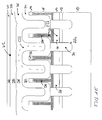
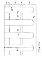
- FIGS. 5A-5C show cross sections of another semiconductor structure for illustrating another approach of the manufacturing method.
- a semiconductor structure is produced according to the PMSS-method.
- the semiconductor structure includes a semiconductor structure 10 , an insulation layer 12 , a layer of floating-gate electrode material 60 , an oxide layer 18 and a nitride layer 20 .
- a semiconductor structure 10 includes a semiconductor structure 10 , an insulation layer 12 , a layer of floating-gate electrode material 60 , an oxide layer 18 and a nitride layer 20 .
- Several examples for the material of the layer of floating-gate electrode material 60 are given above.
- a method of forming a mask of nitride spacers is performed: First, a (not shown) first mask is deposited on the surface of the nitride layer 20 . Some areas of the mask which cover the interspaces of the (later etched) nitride spacers are exposed in a following lithographic step. In a subsequent etching step, nitride spacers 70 a are formed of nitride layer 20 (see broken lines in FIG. 5A ). In a further process step of the FMNS-method, the first mask is removed.
- the width of the nitride spacers 70 a is decreased by an isotropic etch step.
- the newly formed nitride spacers 70 b are shown in FIG. 5A .
- the nitride spacers 70 b serve as a mask during the following RIE step which does not attack the nitride spacers 70 b but etches the material of the layers 18 and 60 .
- RIE step trenches 72 a are etched which extend into the layer of floating-gate electrode material 60 .
- the upper parts of floating-gate electrodes FG with an inverse-T shape are formed of the layer of floating-gate electrode material 60 .
- the RIE step is continued till the bottom of the trenches 72 a is within the distance s 2 from the interface of the layers 12 and 60 .
- the result of the RIE step is shown in FIG. 5B .
- nitride spacers 24 which cover the sidewalls of the trenches 72 a are formed according to FNS-method. Only the bottom of the trenches 72 a is not protected by the nitride spacers 24 .
- a second RIE etch is performed to increase the depth of the trenches 72 a .
- the exposed material at the bottoms of the trenches 72 a is attacked.
- the second RIE step is stopped when the total height h 1 of the trenches 72 b is within a range between 250 nm to 350 nm.
- the newly formed trenches 72 b are partially filled with a STI-fill 30 .
- the nitride spacers 24 are removed by an etching step carried out with hot phosphoric acid.
- the oxide spacers 32 formed on the floating gate electrodes are not removed.
- control-gate electrodes CG and wordlines WL may be formed according to the FCW-method.
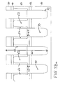
- FIGS. 6A , 6 Ba and 6 Bb show cross sections of another semiconductor structure for illustrating another approach of the manufacturing method.
- a semiconductor structure comprising a semiconductor substrate 10 , an insulation layer 12 , a layer of floating-gate electrode material 60 , an oxide layer 18 and a nitride layer 20 is produced.
- the layer of floating-gate electrode material 60 may include polysilicon and/or at least one transition metal.
- the layer of floating-gate electrode material 60 may include iridium, ruthenium, a transition metal oxide, a transition metal silicide, a transition metal boride, a transition metal aluminide, a transition metal carbide and/or a transition metal nitride. It is also possible to deposit at least two layers of these materials to form floating-gate electrodes FG from their materials according to the method explained below.
- a mask of nitride spacers 70 a is formed of the nitride layer 20 according to the FMNS-method explained above.
- a RIE step is performed to etch the exposed parts of the oxide layer 18 .
- the RIE step is carried out with an etching material that does not attack the nitride spacers 70 a or the material of layer 60 .
- the RIE step is continued till the surface of the layer of floating-gate electrode material 60 is exposed in the interspaces of the nitride spacers 70 a .
- the upper part of trenches 80 a is etched.
- the upper parts of the trenches 80 a have a first width d 5 .
- An isotropic etch step is carried out to etch the lower parts of the trenches 80 a into the layer 60 .
- the lower parts of the trenches 80 a have a second width d 6 that is significantly larger than the first width d 5 .
- the etching material of the isotropic etch step does not attack nitride or oxide. Therefore, the width d 5 of the upper part of the trenches 80 a is not increased significantly during the isotropic etch step.
- the isotropic etch step is continued till the bottom of the trenches 80 a is within the distance s 2 of the insulation layer 12 .
- the result of the isotropic etch step is shown in FIG. 6A .
- nitride spacers 24 which cover the sidewalls of the trenches 80 a are formed according to the FNS-method. These nitride spacers 24 only protect the sidewalls of the trenches 80 a . The bottoms of the trenches 80 a are exposed.
- the unprotected material at the bottoms of the trenches 80 a is etched to increase the depth of the trenches 80 a .
- the RIE step is continued till the etched trenches 80 b extend into the semiconductor substrate 10 and have a total height h 1 in a range between 250 nm to 350 nm.
- the result of the RIE step is shown in FIG. 6 Ba.
- the nitride spacers 24 , the nitride layer 20 and the oxide layer 18 are removed according to the methods explained above and the trenches 80 b are filled with a STI-fill 30 . Then, the FCW-method is performed to form control-gate electrodes CG and wordlines WL on the semiconductor structure.
- the oxide layer 18 may also be etched by the isotropic etch step.
- the oxide spacers 32 are also protected during the following RIE step by the nitride spacers 24 , as can be seen from FIG. 6 Bb.
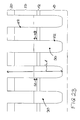
- FIGS. 7A-7F show cross sections of another semiconductor structure for illustrating another approach of the manufacturing method.
- a semiconductor structure is fabricated according to the PMSS-method.
- the semiconductor structure includes a semiconductor substrate 10 , an insulation layer 12 , a layer of floating-gate electrode material 60 , an oxide layer 18 and a nitride layer 20 .
- the layer of floating-gate electrode material 60 may include polysilicon and/or at least one transition metal, for instance a transition metal oxide, a transition metal nitride, a transition metal boride, a transition metal aluminide, a transition metal carbide and/or a transition metal silicide.
- the already mentioned ET-method is carried out to etch trenches 52 into the semiconductor structure.
- These trenches 52 extend from the surface of the semiconductor structure into the semiconductor substrate 10 .
- Their total height h 1 of the trenches 52 may be in a range between 250 nm to 350 nm.
- the semiconductor structure with the trenches 52 is shown in FIG. 7A .
- the trenches 52 are filled with a STI-fill 30 .
- a CMP step may be performed to remove the STI-fill 30 protruding above the nitride layer 20 .
- the STI-fill 30 is partially removed from the trenches 52 till the surface of the STI-fill 30 is near to the surface of layer 60 .
- the sidewalls of the nitride spacers 70 a formed of nitride layers 20 are exposed.
- the mask build of the nitride spacers 70 a is shown (in broken lines) in FIG. 7B .
- This mask of nitride spacers 70 a is used to etch floating-gate electrodes FG.
- an isotropic etch step is performed to decrease the width of the nitride spacers 70 a .
- This isotropic etch step has a rather short duration to make sure that the decrease of the width of the nitride spacers 70 b is rather small, as can be seen from FIG. 7B .
- a RIE step is performed to etch the exposed oxide of the oxide layer 18 and the exposed material of layer 60 .
- This RIE step is continued for a rather short time to make sure that the surface of the STI-fill 30 is moved for a little distance in the direction to the insulation layer 12 .
- the result is shown in FIG. 7B .
- the nitride spacers 70 b are not sensitive against the RIE step. Therefore, the decrease of the nitride spacers 70 b during the RIE step is not significant.
- the width of the nitride spacers 70 b is decreased again by an isotropic etch step.
- the newly formed nitride spacers 70 c are shown in FIG. 7C . (The broken lines mark the former size of the nitride spacers 70 b .)
- the RIE step is repeated, as can be seen from FIG. 7C .
- FIG. 7D shows another intermediate stage of the EFE-method.
- the EFE-method is continued till the surface of the STI-fill 30 is within the distance s 2 of the insulation layer 12 .
- the distance s 2 may be in a range between 10 nm to 30 nm.
- the final shape of the newly etched floating-gate electrodes FG is shown in FIG. 7E .
- the cross sections of the floating-gate electrodes FG are now almost triangular.
- etching steps which specifically attack oxide and/or nitride may be carried out.
- a thermal oxidation may be performed to form silicon oxide layers 82 on the exposed areas of the floating-gate electrodes FG (see FIG. 7E ).
- the silicon oxide layers 82 are then etched away.
- the thermal oxidation and the following etching step may be done to remove damaged material of the floating-gate electrodes FG and to decrease the widths of the floating-gate electrodes FG further.
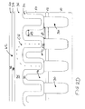
- FIGS. 8A-8F show cross sections of another semiconductor structure for illustrating another approach of the manufacturing method.
- FIG. 8A shows a semiconductor structure comprising a semiconductor substrate 10 , an insulation layer 12 , a layer of floating-gate electrode material 60 , an oxide layer 18 and a nitride layer 20 .
- the semiconductor structure may be produced according to the PMSS-method.
- a mask of nitride spacers 70 a is formed of the nitride layer 20 according to the FMNS-method. Those parts of the oxide layer 18 , which are not protected by the nitride spacers 70 a , are etched away. This is done till some areas of the surface of layer 60 are exposed, as can be seen from FIG. 8A .
- FIGS. 8B and 8C show an intermediate stage and a further stage of the EFE-method.
- a thermal oxidation step is carried out to grow a (not shown) thin oxide layer with a layer thickness about 2 nm on the exposed areas of the floating gate electrodes FG.
- a nitride layer 86 is deposited on the surface of the semiconductor structure.
- a mask is formed on the nitride layer 20 .
- the areas of the mask which cover the bottoms of the trenches 84 are exposed in a lithographic step.
- the nitride layer 86 is removed from the bottoms of the trenches 84 . Only the nitride covering the sidewalls of the floating-gate electrodes FC is protected by the mask during the RIE step. Thus, the nitride spacers 86 shown in FIG. 8D are formed.
- Another RIE step is carried out to etch the exposed material at the bottoms of the trenches 84 and to increase the depth of the trenches 84 .
- This RIE step is continued till the trenches 84 extend into the semiconductor substrate 10 (see FIG. 8E ).
- the total height hi of the trenches 84 is in a range between 250 nm to 350 nm.
- another thermal oxidation step may be carried out.
- at least one etching step is performed to remove the oxide and the nitride from the semiconductor substrate. The result of this at least one etching step is shown in FIG. 8F .
Landscapes
- Semiconductor Memories (AREA)
Abstract
Description
Claims (15)
Priority Applications (1)
| Application Number | Priority Date | Filing Date | Title |
|---|---|---|---|
| US12/104,750 US8258564B2 (en) | 2008-04-17 | 2008-04-17 | Integrated circuit with floating-gate electrodes including a transition metal and corresponding manufacturing method |
Applications Claiming Priority (1)
| Application Number | Priority Date | Filing Date | Title |
|---|---|---|---|
| US12/104,750 US8258564B2 (en) | 2008-04-17 | 2008-04-17 | Integrated circuit with floating-gate electrodes including a transition metal and corresponding manufacturing method |
Publications (2)
| Publication Number | Publication Date |
|---|---|
| US20090261397A1 US20090261397A1 (en) | 2009-10-22 |
| US8258564B2 true US8258564B2 (en) | 2012-09-04 |
Family
ID=41200388
Family Applications (1)
| Application Number | Title | Priority Date | Filing Date |
|---|---|---|---|
| US12/104,750 Active 2030-10-30 US8258564B2 (en) | 2008-04-17 | 2008-04-17 | Integrated circuit with floating-gate electrodes including a transition metal and corresponding manufacturing method |
Country Status (1)
| Country | Link |
|---|---|
| US (1) | US8258564B2 (en) |
Cited By (1)
| Publication number | Priority date | Publication date | Assignee | Title |
|---|---|---|---|---|
| US20180158928A1 (en) * | 2016-12-01 | 2018-06-07 | Semiconductor Manufacturing International (Shanghai) Corporation | Semiconductor device and manufacturing method therefor |
Families Citing this family (2)
| Publication number | Priority date | Publication date | Assignee | Title |
|---|---|---|---|---|
| JP2009094170A (en) | 2007-10-04 | 2009-04-30 | Nec Electronics Corp | Nonvolatile semiconductor memory and method of manufacturing the same |
| US20150263118A1 (en) * | 2014-03-13 | 2015-09-17 | Kabushiki Kaisha Toshiba | Semiconductor memory device and method of manufacturing the same |
Citations (4)
| Publication number | Priority date | Publication date | Assignee | Title |
|---|---|---|---|---|
| US5923976A (en) * | 1995-12-26 | 1999-07-13 | Lg Semicon Co., Ltd. | Nonvolatile memory cell and method of fabricating the same |
| US7615445B2 (en) * | 2006-09-21 | 2009-11-10 | Sandisk Corporation | Methods of reducing coupling between floating gates in nonvolatile memory |
| US7635628B2 (en) * | 2005-02-16 | 2009-12-22 | Samsung Electronics Co., Ltd. | Nonvolatile memory device and method of manufacturing the same |
| US7719065B2 (en) * | 2004-08-26 | 2010-05-18 | Micron Technology, Inc. | Ruthenium layer for a dielectric layer containing a lanthanide oxide |
-
2008
- 2008-04-17 US US12/104,750 patent/US8258564B2/en active Active
Patent Citations (4)
| Publication number | Priority date | Publication date | Assignee | Title |
|---|---|---|---|---|
| US5923976A (en) * | 1995-12-26 | 1999-07-13 | Lg Semicon Co., Ltd. | Nonvolatile memory cell and method of fabricating the same |
| US7719065B2 (en) * | 2004-08-26 | 2010-05-18 | Micron Technology, Inc. | Ruthenium layer for a dielectric layer containing a lanthanide oxide |
| US7635628B2 (en) * | 2005-02-16 | 2009-12-22 | Samsung Electronics Co., Ltd. | Nonvolatile memory device and method of manufacturing the same |
| US7615445B2 (en) * | 2006-09-21 | 2009-11-10 | Sandisk Corporation | Methods of reducing coupling between floating gates in nonvolatile memory |
Cited By (3)
| Publication number | Priority date | Publication date | Assignee | Title |
|---|---|---|---|---|
| US20180158928A1 (en) * | 2016-12-01 | 2018-06-07 | Semiconductor Manufacturing International (Shanghai) Corporation | Semiconductor device and manufacturing method therefor |
| US10522651B2 (en) * | 2016-12-01 | 2019-12-31 | Semiconductor Manufacturing International (Shanghai) Corp. | Semiconductor device and manufacturing method therefor |
| US11069792B2 (en) | 2016-12-01 | 2021-07-20 | Semiconductor Manufacturing (Shanghai) International Corporation | Semiconductor device and manufacturing method therefor |
Also Published As
| Publication number | Publication date |
|---|---|
| US20090261397A1 (en) | 2009-10-22 |
Similar Documents
| Publication | Publication Date | Title |
|---|---|---|
| US7186607B2 (en) | Charge-trapping memory device and method for production | |
| WO2014092943A1 (en) | Air gap isolation in non-volatile memory using sacrificial films | |
| US7960266B2 (en) | Spacer patterns using assist layer for high density semiconductor devices | |
| US7300843B2 (en) | Method of fabricating flash memory device | |
| US8729708B2 (en) | Semiconductor device structures and memory devices including a uniform pattern of conductive material | |
| WO2011156695A1 (en) | Air gap isolation between the bit lines of a non-volatile memory and methods of manufacturing the same | |
| WO2011160011A1 (en) | Isolation between nonvolatile memory cells by means of low- dielectric- constant dielectrics and air gaps and corresponding manufacturing method | |
| US20090155968A1 (en) | Method of forming a dielectric layer pattern and method of manufacturing a non-volatile memory device using the same | |
| US8143156B2 (en) | Methods of forming high density semiconductor devices using recursive spacer technique | |
| TWI324812B (en) | Method for forming self-aligned contacts and local interconnects simultaneously | |
| CN109712980A (en) | The manufacturing method and 3D memory device of 3D memory device | |
| US7592225B2 (en) | Methods of forming spacer patterns using assist layer for high density semiconductor devices | |
| CN100492605C (en) | Method of manufacturing semiconductor device having tungsten gates electrode | |
| TWI396251B (en) | System and method for improving mesa width in a semiconductor device | |
| US8258564B2 (en) | Integrated circuit with floating-gate electrodes including a transition metal and corresponding manufacturing method | |
| US7494860B2 (en) | Methods of forming nonvolatile memories with L-shaped floating gates | |
| JP2006513576A (en) | Improved floating gate insulation and floating gate manufacturing method | |
| JP2003218242A (en) | Non-volatile semiconductor memory device and method of manufacturing the same | |
| EP1786036A1 (en) | Floating gate non-volatile memory cell and process for manufacturing | |
| JP5522915B2 (en) | Semiconductor memory device and manufacturing method thereof | |
| EP2054925A2 (en) | Nonvolatile memories with shaped floating gates | |
| JP2000031305A (en) | And type nonvolatile semiconductor storage device and its manufacture | |
| CN100474567C (en) | Flash memory device and method of manufacturing the same | |
| JP3558571B2 (en) | Method for manufacturing semiconductor device | |
| US7868415B2 (en) | Integrated circuit with an active area line having at least one form-supporting element and corresponding method of making an integrated circuit |
Legal Events
| Date | Code | Title | Description |
|---|---|---|---|
| AS | Assignment |
Owner name: QIMONDA AG, GERMANY Free format text: ASSIGNMENT OF ASSIGNORS INTEREST;ASSIGNORS:WILLER, JOSEF;SPECHT, MICHAEL;FRIEDERICH, CHRISTOPH;AND OTHERS;REEL/FRAME:021162/0653;SIGNING DATES FROM 20080529 TO 20080604 Owner name: QIMONDA FLASH GMBH, GERMANY Free format text: ASSIGNMENT OF ASSIGNORS INTEREST;ASSIGNORS:WILLER, JOSEF;SPECHT, MICHAEL;FRIEDERICH, CHRISTOPH;AND OTHERS;REEL/FRAME:021162/0653;SIGNING DATES FROM 20080529 TO 20080604 Owner name: QIMONDA FLASH GMBH, GERMANY Free format text: ASSIGNMENT OF ASSIGNORS INTEREST;ASSIGNORS:WILLER, JOSEF;SPECHT, MICHAEL;FRIEDERICH, CHRISTOPH;AND OTHERS;SIGNING DATES FROM 20080529 TO 20080604;REEL/FRAME:021162/0653 Owner name: QIMONDA AG, GERMANY Free format text: ASSIGNMENT OF ASSIGNORS INTEREST;ASSIGNORS:WILLER, JOSEF;SPECHT, MICHAEL;FRIEDERICH, CHRISTOPH;AND OTHERS;SIGNING DATES FROM 20080529 TO 20080604;REEL/FRAME:021162/0653 |
|
| AS | Assignment |
Owner name: QIMONDA AG,GERMANY Free format text: ASSIGNMENT OF ASSIGNORS INTEREST;ASSIGNOR:QIMONDA FLASH GMBH;REEL/FRAME:024629/0532 Effective date: 20080808 Owner name: QIMONDA AG, GERMANY Free format text: ASSIGNMENT OF ASSIGNORS INTEREST;ASSIGNOR:QIMONDA FLASH GMBH;REEL/FRAME:024629/0532 Effective date: 20080808 |
|
| STCF | Information on status: patent grant |
Free format text: PATENTED CASE |
|
| FEPP | Fee payment procedure |
Free format text: PAYOR NUMBER ASSIGNED (ORIGINAL EVENT CODE: ASPN); ENTITY STATUS OF PATENT OWNER: LARGE ENTITY |
|
| AS | Assignment |
Owner name: INFINEON TECHNOLOGIES AG, GERMANY Free format text: ASSIGNMENT OF ASSIGNORS INTEREST;ASSIGNOR:QIMONDA AG;REEL/FRAME:035623/0001 Effective date: 20141009 |
|
| AS | Assignment |
Owner name: POLARIS INNOVATIONS LIMITED, IRELAND Free format text: ASSIGNMENT OF ASSIGNORS INTEREST;ASSIGNOR:INFINEON TECHNOLOGIES AG;REEL/FRAME:037254/0782 Effective date: 20150708 |
|
| REMI | Maintenance fee reminder mailed | ||
| FPAY | Fee payment |
Year of fee payment: 4 |
|
| SULP | Surcharge for late payment | ||
| MAFP | Maintenance fee payment |
Free format text: PAYMENT OF MAINTENANCE FEE, 8TH YEAR, LARGE ENTITY (ORIGINAL EVENT CODE: M1552); ENTITY STATUS OF PATENT OWNER: LARGE ENTITY Year of fee payment: 8 |