US8222534B2 - Printed circuit board and manufacturing method thereof - Google Patents
Printed circuit board and manufacturing method thereof Download PDFInfo
- Publication number
- US8222534B2 US8222534B2 US12/076,118 US7611808A US8222534B2 US 8222534 B2 US8222534 B2 US 8222534B2 US 7611808 A US7611808 A US 7611808A US 8222534 B2 US8222534 B2 US 8222534B2
- Authority
- US
- United States
- Prior art keywords
- board
- bump
- insulation layer
- printed circuit
- forming
- Prior art date
- Legal status (The legal status is an assumption and is not a legal conclusion. Google has not performed a legal analysis and makes no representation as to the accuracy of the status listed.)
- Expired - Fee Related, expires
Links
Images


Classifications
-
- H—ELECTRICITY
- H05—ELECTRIC TECHNIQUES NOT OTHERWISE PROVIDED FOR
- H05K—PRINTED CIRCUITS; CASINGS OR CONSTRUCTIONAL DETAILS OF ELECTRIC APPARATUS; MANUFACTURE OF ASSEMBLAGES OF ELECTRICAL COMPONENTS
- H05K3/00—Apparatus or processes for manufacturing printed circuits
- H05K3/46—Manufacturing multilayer circuits
- H05K3/4611—Manufacturing multilayer circuits by laminating two or more circuit boards
- H05K3/4614—Manufacturing multilayer circuits by laminating two or more circuit boards the electrical connections between the circuit boards being made during lamination
-
- H—ELECTRICITY
- H05—ELECTRIC TECHNIQUES NOT OTHERWISE PROVIDED FOR
- H05K—PRINTED CIRCUITS; CASINGS OR CONSTRUCTIONAL DETAILS OF ELECTRIC APPARATUS; MANUFACTURE OF ASSEMBLAGES OF ELECTRICAL COMPONENTS
- H05K3/00—Apparatus or processes for manufacturing printed circuits
- H05K3/40—Forming printed elements for providing electric connections to or between printed circuits
- H05K3/42—Plated through-holes or plated via connections
-
- H—ELECTRICITY
- H05—ELECTRIC TECHNIQUES NOT OTHERWISE PROVIDED FOR
- H05K—PRINTED CIRCUITS; CASINGS OR CONSTRUCTIONAL DETAILS OF ELECTRIC APPARATUS; MANUFACTURE OF ASSEMBLAGES OF ELECTRICAL COMPONENTS
- H05K3/00—Apparatus or processes for manufacturing printed circuits
- H05K3/46—Manufacturing multilayer circuits
- H05K3/4611—Manufacturing multilayer circuits by laminating two or more circuit boards
- H05K3/4614—Manufacturing multilayer circuits by laminating two or more circuit boards the electrical connections between the circuit boards being made during lamination
- H05K3/462—Manufacturing multilayer circuits by laminating two or more circuit boards the electrical connections between the circuit boards being made during lamination characterized by laminating only or mainly similar double-sided circuit boards
-
- H—ELECTRICITY
- H05—ELECTRIC TECHNIQUES NOT OTHERWISE PROVIDED FOR
- H05K—PRINTED CIRCUITS; CASINGS OR CONSTRUCTIONAL DETAILS OF ELECTRIC APPARATUS; MANUFACTURE OF ASSEMBLAGES OF ELECTRICAL COMPONENTS
- H05K2201/00—Indexing scheme relating to printed circuits covered by H05K1/00
- H05K2201/09—Shape and layout
- H05K2201/09209—Shape and layout details of conductors
- H05K2201/095—Conductive through-holes or vias
- H05K2201/09509—Blind vias, i.e. vias having one side closed
-
- H—ELECTRICITY
- H05—ELECTRIC TECHNIQUES NOT OTHERWISE PROVIDED FOR
- H05K—PRINTED CIRCUITS; CASINGS OR CONSTRUCTIONAL DETAILS OF ELECTRIC APPARATUS; MANUFACTURE OF ASSEMBLAGES OF ELECTRICAL COMPONENTS
- H05K2201/00—Indexing scheme relating to printed circuits covered by H05K1/00
- H05K2201/09—Shape and layout
- H05K2201/09209—Shape and layout details of conductors
- H05K2201/095—Conductive through-holes or vias
- H05K2201/09536—Buried plated through-holes, i.e. plated through-holes formed in a core before lamination
-
- H—ELECTRICITY
- H05—ELECTRIC TECHNIQUES NOT OTHERWISE PROVIDED FOR
- H05K—PRINTED CIRCUITS; CASINGS OR CONSTRUCTIONAL DETAILS OF ELECTRIC APPARATUS; MANUFACTURE OF ASSEMBLAGES OF ELECTRICAL COMPONENTS
- H05K2201/00—Indexing scheme relating to printed circuits covered by H05K1/00
- H05K2201/09—Shape and layout
- H05K2201/09209—Shape and layout details of conductors
- H05K2201/095—Conductive through-holes or vias
- H05K2201/096—Vertically aligned vias, holes or stacked vias
-
- H—ELECTRICITY
- H05—ELECTRIC TECHNIQUES NOT OTHERWISE PROVIDED FOR
- H05K—PRINTED CIRCUITS; CASINGS OR CONSTRUCTIONAL DETAILS OF ELECTRIC APPARATUS; MANUFACTURE OF ASSEMBLAGES OF ELECTRICAL COMPONENTS
- H05K2201/00—Indexing scheme relating to printed circuits covered by H05K1/00
- H05K2201/09—Shape and layout
- H05K2201/09209—Shape and layout details of conductors
- H05K2201/09654—Shape and layout details of conductors covering at least two types of conductors provided for in H05K2201/09218 - H05K2201/095
- H05K2201/09781—Dummy conductors, i.e. not used for normal transport of current; Dummy electrodes of components
-
- H—ELECTRICITY
- H05—ELECTRIC TECHNIQUES NOT OTHERWISE PROVIDED FOR
- H05K—PRINTED CIRCUITS; CASINGS OR CONSTRUCTIONAL DETAILS OF ELECTRIC APPARATUS; MANUFACTURE OF ASSEMBLAGES OF ELECTRICAL COMPONENTS
- H05K2203/00—Indexing scheme relating to apparatus or processes for manufacturing printed circuits covered by H05K3/00
- H05K2203/05—Patterning and lithography; Masks; Details of resist
- H05K2203/0548—Masks
- H05K2203/0554—Metal used as mask for etching vias, e.g. by laser ablation
-
- H—ELECTRICITY
- H05—ELECTRIC TECHNIQUES NOT OTHERWISE PROVIDED FOR
- H05K—PRINTED CIRCUITS; CASINGS OR CONSTRUCTIONAL DETAILS OF ELECTRIC APPARATUS; MANUFACTURE OF ASSEMBLAGES OF ELECTRICAL COMPONENTS
- H05K2203/00—Indexing scheme relating to apparatus or processes for manufacturing printed circuits covered by H05K3/00
- H05K2203/06—Lamination
- H05K2203/061—Lamination of previously made multilayered subassemblies
-
- H—ELECTRICITY
- H05—ELECTRIC TECHNIQUES NOT OTHERWISE PROVIDED FOR
- H05K—PRINTED CIRCUITS; CASINGS OR CONSTRUCTIONAL DETAILS OF ELECTRIC APPARATUS; MANUFACTURE OF ASSEMBLAGES OF ELECTRICAL COMPONENTS
- H05K3/00—Apparatus or processes for manufacturing printed circuits
- H05K3/0011—Working of insulating substrates or insulating layers
- H05K3/0017—Etching of the substrate by chemical or physical means
- H05K3/0026—Etching of the substrate by chemical or physical means by laser ablation
- H05K3/0032—Etching of the substrate by chemical or physical means by laser ablation of organic insulating material
- H05K3/0035—Etching of the substrate by chemical or physical means by laser ablation of organic insulating material of blind holes, i.e. having a metal layer at the bottom
-
- H—ELECTRICITY
- H05—ELECTRIC TECHNIQUES NOT OTHERWISE PROVIDED FOR
- H05K—PRINTED CIRCUITS; CASINGS OR CONSTRUCTIONAL DETAILS OF ELECTRIC APPARATUS; MANUFACTURE OF ASSEMBLAGES OF ELECTRICAL COMPONENTS
- H05K3/00—Apparatus or processes for manufacturing printed circuits
- H05K3/40—Forming printed elements for providing electric connections to or between printed circuits
- H05K3/4038—Through-connections; Vertical interconnect access [VIA] connections
- H05K3/4053—Through-connections; Vertical interconnect access [VIA] connections by thick-film techniques
- H05K3/4069—Through-connections; Vertical interconnect access [VIA] connections by thick-film techniques for via connections in organic insulating substrates
-
- H—ELECTRICITY
- H05—ELECTRIC TECHNIQUES NOT OTHERWISE PROVIDED FOR
- H05K—PRINTED CIRCUITS; CASINGS OR CONSTRUCTIONAL DETAILS OF ELECTRIC APPARATUS; MANUFACTURE OF ASSEMBLAGES OF ELECTRICAL COMPONENTS
- H05K3/00—Apparatus or processes for manufacturing printed circuits
- H05K3/46—Manufacturing multilayer circuits
- H05K3/4602—Manufacturing multilayer circuits characterized by a special circuit board as base or central core whereon additional circuit layers are built or additional circuit boards are laminated
-
- H—ELECTRICITY
- H05—ELECTRIC TECHNIQUES NOT OTHERWISE PROVIDED FOR
- H05K—PRINTED CIRCUITS; CASINGS OR CONSTRUCTIONAL DETAILS OF ELECTRIC APPARATUS; MANUFACTURE OF ASSEMBLAGES OF ELECTRICAL COMPONENTS
- H05K3/00—Apparatus or processes for manufacturing printed circuits
- H05K3/46—Manufacturing multilayer circuits
- H05K3/4611—Manufacturing multilayer circuits by laminating two or more circuit boards
- H05K3/4623—Manufacturing multilayer circuits by laminating two or more circuit boards the circuit boards having internal via connections between two or more circuit layers before lamination, e.g. double-sided circuit boards
-
- H—ELECTRICITY
- H05—ELECTRIC TECHNIQUES NOT OTHERWISE PROVIDED FOR
- H05K—PRINTED CIRCUITS; CASINGS OR CONSTRUCTIONAL DETAILS OF ELECTRIC APPARATUS; MANUFACTURE OF ASSEMBLAGES OF ELECTRICAL COMPONENTS
- H05K3/00—Apparatus or processes for manufacturing printed circuits
- H05K3/46—Manufacturing multilayer circuits
- H05K3/4644—Manufacturing multilayer circuits by building the multilayer layer by layer, i.e. build-up multilayer circuits
- H05K3/4647—Manufacturing multilayer circuits by building the multilayer layer by layer, i.e. build-up multilayer circuits by applying an insulating layer around previously made via studs
-
- Y—GENERAL TAGGING OF NEW TECHNOLOGICAL DEVELOPMENTS; GENERAL TAGGING OF CROSS-SECTIONAL TECHNOLOGIES SPANNING OVER SEVERAL SECTIONS OF THE IPC; TECHNICAL SUBJECTS COVERED BY FORMER USPC CROSS-REFERENCE ART COLLECTIONS [XRACs] AND DIGESTS
- Y10—TECHNICAL SUBJECTS COVERED BY FORMER USPC
- Y10T—TECHNICAL SUBJECTS COVERED BY FORMER US CLASSIFICATION
- Y10T29/00—Metal working
- Y10T29/49—Method of mechanical manufacture
- Y10T29/49002—Electrical device making
- Y10T29/49117—Conductor or circuit manufacturing
- Y10T29/49124—On flat or curved insulated base, e.g., printed circuit, etc.
- Y10T29/49155—Manufacturing circuit on or in base
- Y10T29/49156—Manufacturing circuit on or in base with selective destruction of conductive paths
Definitions
- the present invention relates to a printed circuit board and to a method of manufacturing the printed circuit board.
- FIGS. 1A to 1H one method currently being used to manufacture a high-density printed circuit board is illustrated in FIGS. 1A to 1H , which includes forming bumps 3 on a board 2 , stacking on an insulation layer 4 , and stacking this in turn onto a multi-layer board 1 , etc., while applying heat and pressure.
- This is referred to as a B2it method.
- vias for interlayer conduction can be formed in a simple manner, whereby manufacturing efficiency can be increased.
- the B2it method includes forming paste bumps, using copper (Cu), silver (Ag), etc., on a copper foil, piling an insulation layer with the copper foil, and then applying heat and pressure for stacking.
- the process of printing the paste has to be performed such that the bumps have a height sufficient to penetrate the insulation layer.
- the conductive paste 3 a , 3 b may be printed on the lands 9 formed on an insulation layer 4 ′ over a series of four or five repetitions.
- the repeated printing intended for forming the bumps to a particular height can lower productivity, and can cause spreading at the lower ends of the bumps.
- An aspect of the invention is to provide a printed circuit board and a method of manufacturing the printed circuit board, which improve productivity and resolve the problem of spreading.
- One aspect of the invention provides a method of manufacturing a printed circuit board by forming at least one bump for interlayer conduction on a surface of a board and stacking an insulation layer on the surface of the board.
- the method includes forming at least one dam on the surface of the board that surrounds a region corresponding to the bump, forming the bump by printing conductive paste onto the region corresponding to the bump, and stacking the insulation layer onto the surface of the board.
- Forming the dam can be performed by selectively etching a metal layer stacked on the surface of the board, and the dam can be made of a material including copper.
- Another aspect of the invention provides a printed circuit board that includes a board, a bump formed on a surface of the board, a dam formed on the surface of the board that surrounds an edge of the bump, and a first insulation layer stacked on the surface of the board.
- the board can be a copper clad laminate (CCL), which has a copper foil stacked on a second insulation layer, in which case the dam may be shaped by selectively removing the copper foil.
- CCL copper clad laminate
- FIG. 1A , FIG. 1B , FIG. 1C , FIG. 1D , FIG. 1E , FIG. 1F , FIG. 1G , and FIG. 1H are cross-sectional views representing a flow diagram for a method of manufacturing a printed circuit board according to the related art.
- FIG. 2A and FIG. 2B are cross-sectional views representing a flow diagram for a method of forming bumps according to the related art.
- FIG. 3 is a flowchart illustrating a method of manufacturing a printed circuit board according to an aspect of the invention.
- FIG. 4A , FIG. 4B , FIG. 4C , FIG. 4D , FIG. 4E , FIG. 4F , FIG. 4G , and FIG. 4H are cross-sectional views representing a flow diagram for the method illustrated in FIG. 3 .
- FIG. 5 is a plan view illustrating a board on which dams have been formed.
- FIG. 6A and FIG. 6B are cross-sectional views representing a flow diagram for a method of forming bumps.
- FIG. 7 is a cross-sectional view of a printed circuit board according to another aspect of the invention.
- FIG. 3 is a flowchart illustrating a method of manufacturing a printed circuit board according to an aspect of the invention
- FIG. 4A through FIG. 4H are cross-sectional views representing a flow diagram for the method illustrated in FIG. 3 .
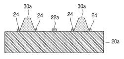
- FIGS. 4A to 4H are illustrated a four-layer board 10 , insulation layers 20 a , 20 b , patterns 22 a , 22 b , dams 24 , bumps 30 , and bump boards 40 .
- dams 24 may be formed, which surround regions corresponding to bumps 30 , on a surface of a board (S 10 ).
- the board may provide the position where the bumps 30 are to be formed, and in this particular embodiment, an insulation layer 20 a can be used for the board.
- the board can take a form other than an insulation layer 20 a .
- a double-sided printed circuit board can be used that already has particular patterns formed on either side.
- the insulation layer 20 a may serve to electrically insulate the upper and lower layers of the printed circuit board.
- a particular pattern may be formed on the lower surface of the insulation layer 20 a , and may even have several layers of boards stacked thereon.
- a dam 24 can serve to confine the region of a bump that interconnects layers, as well as to provide support for the bump 30 .
- a method of forming the dams 24 will be described in more detail as follows.
- an etching resist may be formed on a metal layer (not shown) stacked on a surface of the insulation layer 20 a (S 11 ).
- the etching resist (not shown) can be formed to cover the metal layer (not shown) in positions where the dams 24 are to be formed.
- This etching resist (not shown) can be formed using a mask, by a method of exposure and development, etc.
- a copper clad laminate (CCL) which has a copper foil stacked on either side of an insulating layer, can be used for the insulation layer 20 a and the metal layer (not shown) stacked on the insulation layers 20 a.
- an etchant may be provided (S 12 ). Using an etchant, the portions other than those portions covered by the etching resist (not shown) can be removed. Afterwards, the etching resist (not shown) may be removed (S 13 ).
- the dams 24 can be formed simultaneously during the process for forming the patterns 22 a , etc., on the insulation layer 20 a . As such, since there is no need for a separate process in forming the dams 24 , the manufacturing process can be simplified.
- An example of the patterns 22 a and dams 24 formed on the insulation layer 20 a is illustrated in FIG. 4B and FIG. 5 .
- conductive paste may be printed to form the bumps 30 (S 20 ). As illustrated in FIGS. 6A and 6B , the regions where the conductive paste 30 a , 30 b are printed may be surrounded by the dams 24 . Therefore, during the procedure for forming the bumps 30 by printing the conductive paste 30 a , 30 b , the lower ends of the bumps 30 may be supported by the dams 24 , and the areas of the board occupied by the bumps 30 can be limited by the dams 24 .
- the number of repetitions of printing for forming the bumps 30 to a particular height can be reduced, to confer an aspect of increased productivity.
- the results of repeatedly printing the conductive paste 30 a , 30 b are illustrated in FIGS. 6A and 6B , and the bumps 30 thus formed can be seen also in FIG. 4C .
- an insulation layer may be stacked on to form a bump board (S 30 ).
- the insulation layer 20 b can be stacked over the insulation layer 20 a on which the bumps 30 and the pattern 22 a are formed, where the bumps 30 can be made to penetrate the insulation layer 20 b .
- the insulation layer 20 b may serve to provide electrical insulation between layers, and can be made, for example, from Prepreg.
- Bump boards 40 formed as above may be stacked onto a four-layer board 10 , as illustrated in FIG. 4E , to implement a multi-layer printed circuit board such as that illustrated in FIG. 4F .
- holes 26 can be perforated in the outermost layers, as illustrated in FIG. 4G , and interlayer conduction can be provided at the outermost layers using a method such as forming plating layers 28 in the holes 26 .
- FIG. 7 is a cross-sectional view of a printed circuit board according to another aspect of the invention.
- a four-layer board 10 insulation layers 20 a , 20 b , patterns 22 a , 22 b , dams 24 , bumps 30 , and bump boards 40 .
- conduction between layers can be implemented by elements including the bumps 30 which penetrate the insulation layers, and the plating layers which are formed in the holes 26 .
- a dam 24 can be formed around the edge of a bump 30 to surround the bump 30 , where such dams 24 may facilitate the forming of the bumps 30 while preventing spreading.
- the insulation layers 20 a , on which the dams 24 are formed, and the patterns 22 a , 22 b formed on these insulation layers 20 a can be formed by selectively removing the copper foils of a copper clad laminate, where the dams 24 can be formed by the same method, as already described above.
Abstract
Description
Claims (3)
Applications Claiming Priority (2)
| Application Number | Priority Date | Filing Date | Title |
|---|---|---|---|
| KR10-2007-0059323 | 2007-06-18 | ||
| KR1020070059323A KR100850763B1 (en) | 2007-06-18 | 2007-06-18 | Printed circuit board and manufacturing method thereof |
Publications (2)
| Publication Number | Publication Date |
|---|---|
| US20080310132A1 US20080310132A1 (en) | 2008-12-18 |
| US8222534B2 true US8222534B2 (en) | 2012-07-17 |
Family
ID=39881296
Family Applications (1)
| Application Number | Title | Priority Date | Filing Date |
|---|---|---|---|
| US12/076,118 Expired - Fee Related US8222534B2 (en) | 2007-06-18 | 2008-03-13 | Printed circuit board and manufacturing method thereof |
Country Status (3)
| Country | Link |
|---|---|
| US (1) | US8222534B2 (en) |
| JP (1) | JP4553950B2 (en) |
| KR (1) | KR100850763B1 (en) |
Families Citing this family (2)
| Publication number | Priority date | Publication date | Assignee | Title |
|---|---|---|---|---|
| KR100761706B1 (en) * | 2006-09-06 | 2007-09-28 | 삼성전기주식회사 | Fabrication method for printed circuit board |
| US8314473B2 (en) * | 2010-05-04 | 2012-11-20 | Fairchild Semiconductor Corporation | Die backside standoff structures for semiconductor devices |
Citations (9)
| Publication number | Priority date | Publication date | Assignee | Title |
|---|---|---|---|---|
| JPH08293661A (en) | 1995-04-21 | 1996-11-05 | Sumitomo Metal Ind Ltd | Ceramic circuit board and manufacture thereof |
| US5976699A (en) * | 1995-11-09 | 1999-11-02 | Sumitomo Bakelite Company Limited | Insulating adhesive for multilayer printed circuit board |
| US6191489B1 (en) * | 1999-02-19 | 2001-02-20 | Micronas Gmbh | Micromechanical layer stack arrangement particularly for flip chip or similar connections |
| JP2002290048A (en) | 2001-03-23 | 2002-10-04 | Fujitsu Ltd | Via forming method in multilayer circuit board |
| US20020145178A1 (en) * | 2001-04-05 | 2002-10-10 | Taiwan Semiconductor Manufacturing Co., Ltd. | Matrix form semiconductor package substrate having an electrode of serpentine shape and method for forming |
| US20040233035A1 (en) * | 1996-04-18 | 2004-11-25 | Tessera, Inc. | Methods for manufacturing resistors using a sacrificial layer |
| US6921715B2 (en) * | 2003-05-02 | 2005-07-26 | Yu-Nung Shen | Semiconductor package and method of fabricating same |
| KR20070025496A (en) | 2005-09-02 | 2007-03-08 | 삼성전기주식회사 | Manufacturing method of printed circuit board |
| US7230339B2 (en) * | 2003-03-28 | 2007-06-12 | Intel Corporation | Copper ring solder mask defined ball grid array pad |
Family Cites Families (1)
| Publication number | Priority date | Publication date | Assignee | Title |
|---|---|---|---|---|
| KR100632558B1 (en) * | 2004-12-29 | 2006-10-11 | 삼성전기주식회사 | Improved vacuum press apparatus and method |
-
2007
- 2007-06-18 KR KR1020070059323A patent/KR100850763B1/en not_active IP Right Cessation
-
2008
- 2008-03-13 US US12/076,118 patent/US8222534B2/en not_active Expired - Fee Related
- 2008-04-01 JP JP2008095405A patent/JP4553950B2/en not_active Expired - Fee Related
Patent Citations (9)
| Publication number | Priority date | Publication date | Assignee | Title |
|---|---|---|---|---|
| JPH08293661A (en) | 1995-04-21 | 1996-11-05 | Sumitomo Metal Ind Ltd | Ceramic circuit board and manufacture thereof |
| US5976699A (en) * | 1995-11-09 | 1999-11-02 | Sumitomo Bakelite Company Limited | Insulating adhesive for multilayer printed circuit board |
| US20040233035A1 (en) * | 1996-04-18 | 2004-11-25 | Tessera, Inc. | Methods for manufacturing resistors using a sacrificial layer |
| US6191489B1 (en) * | 1999-02-19 | 2001-02-20 | Micronas Gmbh | Micromechanical layer stack arrangement particularly for flip chip or similar connections |
| JP2002290048A (en) | 2001-03-23 | 2002-10-04 | Fujitsu Ltd | Via forming method in multilayer circuit board |
| US20020145178A1 (en) * | 2001-04-05 | 2002-10-10 | Taiwan Semiconductor Manufacturing Co., Ltd. | Matrix form semiconductor package substrate having an electrode of serpentine shape and method for forming |
| US7230339B2 (en) * | 2003-03-28 | 2007-06-12 | Intel Corporation | Copper ring solder mask defined ball grid array pad |
| US6921715B2 (en) * | 2003-05-02 | 2005-07-26 | Yu-Nung Shen | Semiconductor package and method of fabricating same |
| KR20070025496A (en) | 2005-09-02 | 2007-03-08 | 삼성전기주식회사 | Manufacturing method of printed circuit board |
Non-Patent Citations (2)
| Title |
|---|
| Japanese Office Action issued Mar. 16, 2010 in corresponding Japanese Patent Application 2008-095405. |
| Office Action mailed on Mar. 26, 2008 and issued in corresponding Korean Patent Application No. 10-2007-0059323. |
Also Published As
| Publication number | Publication date |
|---|---|
| JP4553950B2 (en) | 2010-09-29 |
| US20080310132A1 (en) | 2008-12-18 |
| KR100850763B1 (en) | 2008-08-06 |
| JP2008311619A (en) | 2008-12-25 |
Similar Documents
| Publication | Publication Date | Title |
|---|---|---|
| KR100754080B1 (en) | Rigid-flexible printed circuit board and manufacturing method therefor | |
| US10039184B2 (en) | Circuit board structure and manufacturing method thereof | |
| US20070107934A1 (en) | Printed circuit board using paste bump and manufacturing method thereof | |
| KR101281410B1 (en) | Multilayer Wiring Substrate | |
| JP5080234B2 (en) | Wiring board and manufacturing method thereof | |
| TWI617225B (en) | Printed circuit board and method for manufacturing the same | |
| JP2006100789A (en) | Manufacturing method of electric wiring structure | |
| JP5693339B2 (en) | Multilayer printed wiring board and manufacturing method thereof | |
| JP2008311612A (en) | Multilayer printed circuit board, and method of manufacturing the same | |
| US8222534B2 (en) | Printed circuit board and manufacturing method thereof | |
| JP2013106034A (en) | Manufacturing method of printed circuit board | |
| CN104703399A (en) | Circuit board and production method thereof | |
| JP2007214568A (en) | Circuit board structure | |
| JP2008016630A (en) | Printed circuit board, and its manufacturing method | |
| JP2007165863A (en) | Via hole having minute hole land and method of forming same | |
| JP3965148B2 (en) | Printed wiring board for mounting electronic components, method for manufacturing the same, and semiconductor device | |
| KR101283164B1 (en) | The printed circuit board and the method for manufacturing the same | |
| KR101171100B1 (en) | Manufacturing method for circuit board | |
| JP2023113472A (en) | Printed circuit board and manufacturing method thereof | |
| TWI301734B (en) | Circuit board structure and fabricating method thereof | |
| CN107708292B (en) | PCB capable of effectively reducing buried hole cracks and manufacturing method thereof | |
| KR101088062B1 (en) | A build-up printed circuit board of stack type using bump structure and manufacturing method of the same | |
| KR100652132B1 (en) | Printed circuit board and Method of manufacturing the same | |
| KR101262534B1 (en) | The printed circuit board and the method for manufacturing the same | |
| JP4337456B2 (en) | Capacitor built-in wiring circuit board and manufacturing method thereof |
Legal Events
| Date | Code | Title | Description |
|---|---|---|---|
| AS | Assignment |
Owner name: SAMSUNG ELECTRO-MECHANICS CO., LTD., KOREA, REPUBL Free format text: ASSIGNMENT OF ASSIGNORS INTEREST;ASSIGNORS:PARK, JUN-HEYOUNG;MOK, JEE-SOO;KIM, KI-HWAN;AND OTHERS;REEL/FRAME:020685/0685 Effective date: 20080211 |
|
| FEPP | Fee payment procedure |
Free format text: PAYOR NUMBER ASSIGNED (ORIGINAL EVENT CODE: ASPN); ENTITY STATUS OF PATENT OWNER: LARGE ENTITY |
|
| STCF | Information on status: patent grant |
Free format text: PATENTED CASE |
|
| FPAY | Fee payment |
Year of fee payment: 4 |
|
| FEPP | Fee payment procedure |
Free format text: MAINTENANCE FEE REMINDER MAILED (ORIGINAL EVENT CODE: REM.); ENTITY STATUS OF PATENT OWNER: LARGE ENTITY |
|
| LAPS | Lapse for failure to pay maintenance fees |
Free format text: PATENT EXPIRED FOR FAILURE TO PAY MAINTENANCE FEES (ORIGINAL EVENT CODE: EXP.); ENTITY STATUS OF PATENT OWNER: LARGE ENTITY |
|
| STCH | Information on status: patent discontinuation |
Free format text: PATENT EXPIRED DUE TO NONPAYMENT OF MAINTENANCE FEES UNDER 37 CFR 1.362 |
|
| FP | Lapsed due to failure to pay maintenance fee |
Effective date: 20200717 |