US8188760B2 - Curve tracer signal conversion for integrated circuit testing - Google Patents
Curve tracer signal conversion for integrated circuit testing Download PDFInfo
- Publication number
- US8188760B2 US8188760B2 US12/551,524 US55152409A US8188760B2 US 8188760 B2 US8188760 B2 US 8188760B2 US 55152409 A US55152409 A US 55152409A US 8188760 B2 US8188760 B2 US 8188760B2
- Authority
- US
- United States
- Prior art keywords
- reference voltage
- input
- curve tracer
- port
- collector
- Prior art date
- Legal status (The legal status is an assumption and is not a legal conclusion. Google has not performed a legal analysis and makes no representation as to the accuracy of the status listed.)
- Expired - Fee Related, expires
Links
Images


Classifications
-
- G—PHYSICS
- G01—MEASURING; TESTING
- G01R—MEASURING ELECTRIC VARIABLES; MEASURING MAGNETIC VARIABLES
- G01R31/00—Arrangements for testing electric properties; Arrangements for locating electric faults; Arrangements for electrical testing characterised by what is being tested not provided for elsewhere
- G01R31/28—Testing of electronic circuits, e.g. by signal tracer
- G01R31/2832—Specific tests of electronic circuits not provided for elsewhere
- G01R31/2836—Fault-finding or characterising
- G01R31/2837—Characterising or performance testing, e.g. of frequency response
-
- G—PHYSICS
- G01—MEASURING; TESTING
- G01R—MEASURING ELECTRIC VARIABLES; MEASURING MAGNETIC VARIABLES
- G01R31/00—Arrangements for testing electric properties; Arrangements for locating electric faults; Arrangements for electrical testing characterised by what is being tested not provided for elsewhere
- G01R31/26—Testing of individual semiconductor devices
- G01R31/2607—Circuits therefor
-
- G—PHYSICS
- G01—MEASURING; TESTING
- G01R—MEASURING ELECTRIC VARIABLES; MEASURING MAGNETIC VARIABLES
- G01R31/00—Arrangements for testing electric properties; Arrangements for locating electric faults; Arrangements for electrical testing characterised by what is being tested not provided for elsewhere
- G01R31/28—Testing of electronic circuits, e.g. by signal tracer
- G01R31/2851—Testing of integrated circuits [IC]
- G01R31/2886—Features relating to contacting the IC under test, e.g. probe heads; chucks
Definitions
- This invention generally relates to integrated circuit (IC) test fixtures and, more particularly, to a universal socketless test fixture using a curve tracer and an associated conversion device to supply fixture test signals.
- IC integrated circuit
- IC devices have evolved from through-board pins to the surface mounting of a device to a socket and PCB.
- the input and output contacts of an IC chip are generally disposed in grid-like patterns that substantially cover a surface of the device or in elongated rows which may extend parallel to and adjacent each edge of the device's front surface, or in the center of the front surface.
- devices such as chips must be physically mounted on a substrate such as a printed circuit board, and the contacts of the device must be electrically connected to electrically conductive features of the circuit board.
- surface mounted packages commonly include a dielectric element, commonly referred to as a “chip carrier” with terminals formed as plated or etched metallic structures on the dielectric. These terminals are typically connected to the contacts of the chip itself by features such as thin traces extending along the chip carrier itself and by fine leads or wires extending between the contacts of the chip and the terminals or traces.
- the package is placed onto a circuit board so that each terminal on the package is aligned with a corresponding contact pad on the circuit board. Solder or other bonding material is provided between the terminals and the contact pads.
- the package can be permanently bonded in place by heating the assembly so as to melt or “reflow” the solder or otherwise activate the bonding material.
- solder chips are commonly provided in packages that facilitate handling of the chip during manufacture and during mounting of the chip on an external substrate such as a circuit board or other circuit panel.
- An IC that is designed to be surface mounted has pads, or flat conductive discs, on its packaging.
- Many packages include solder masses in the form of solder balls, typically about 1.0 mm and about 0.8 mm (40 mils and 30 mils) in pitch, and 0.4 to 0.5 mm in diameter, attached to the terminals of the package.
- a package having an array of solder balls projecting from its bottom surface is commonly referred to as a ball grid array or “BGA” package.
- BGA ball grid array
- solder bumps typically fit into grips on a BGA socket for connection to a PCB.
- Other packages referred to as land grid array or “LGA” packages are secured to the substrate by thin layers or lands (pads) formed from solder.
- the pads of an LGA require a socket containing springs or some other type of conductive trace to connect the device to the PCB.
- a socket is typically used to interface IC contacts to a test fixture.
- a socket may have a plastic body, metal contacts, and a metal lever or latch to temporary secure the IC to the socket—physically securing the IC under test, as well as causing an electrical connection between all the IC pins and the socket.
- a test fixture may consist of an array of switch pairs, where one switch connects a single signal trace to a single power trace and the other switch connects the signal trace to a single ground trace. Multiple switch pairs are used to connect all signal traces to independent power and ground traces. Typically, the sockets make electric connections to all the device pins simultaneously. Automation of the process requires a relay/relay driver circuit for each device pin.
- test fixture uses a socket designed for the specific pin count and physical spacing of the package pins.
- these test fixture are often custom made and, therefore, expensive.
- a test facility may require a multiplicity of sockets and interface boards for a large variety of package types.
- socket interfaces it becomes prohibitively expensive to upgrade the electrical components of the test fixture, to support complicated test algorithms such as curve tracing.
- Testing may be supported through the use of a conventional curve tracer. Without a socket, however, hand probing of each pair of device pins is required, which does not lend itself to efficient automated data collection on high pin count packages.
- a clip-on mechanism with a hook-shaped wire is known to be used in connecting to individual IC contacts.
- the spring loading is within a rigid plastic housing that is too large to fit in the spaces between the BGA rows. Alternately, micromanipulators with needle probes must be used.
- test fixture that provides a means to make contact to many pins of a packaged IC, without the use of a socket, permitting curve tracer analysis on all pins contacted and real-time interactive curve tracer analysis.
- the test fixture reduces the need for high pin-count sockets.
- the real-time examination of electrical characteristics is enabled.
- defects can be observed such as drift, intermittence, and noise, which are unstable and change in a short time frame.
- This analysis is not available with conventional fully automated curve trace analysis. Further, the cost of high pin count automated curve tracer systems, and high pin count sockets are prohibitively high.
- a conventional manual curve tracer displays curves for one device pin at a time.
- the waveform at the base generator terminal provides a stair step waveform of up to ten steps. These steps typically drive the same pin of a transistor under test at ten different base current (or voltages for an FET transistor).
- the resultant curves are displayed simultaneously as a family of curves.
- a curve tracer signal conversion device is presented herein that generates timing and control signals from the base generator terminal output of a conventional curve tracer, to permit the viewing and storage of multiple device pin traces, instead of just one. As a result, it is possible to quickly measure curve tracing from a high pin count devices.
- the measurement and storage process can be completely automated when combined with automated probe card movement.
- the base terminal waveform is a voltage stair step, which is converted into a sequence of clock pulses, followed by a reset pulse at the end of the stair step waveform.
- These clock pulses and reset pulses drive a decade counter, and the decade counter outputs drive relays.
- the common node of each relay is connected to the collector terminal of the curve tracer, and selectively connected to the individual pins of the device under test (DUT). Because the pulses are synchronized from the base terminal waveform, the relay switch time is coincident with the step waveforms that are presented on the curve tracer display. Thus, each curve on the curve tracer display (and in memory) is associated with a different pin of the DUT.
- a curve tracer signal conversion device has an input connected to the curve tracer base port to accept a repeating sequence of stepped base signals.
- the conversion device has a signal input connected to either the curve tracer collector or emitter port, typically the collector.
- the conversion device has a plurality of signal outputs, where each signal output is sequentially connected to the selected (i.e. collector) curve tracer port in response to a corresponding base step signal.
- the conversion device includes a high pass filter connected to a curve tracer base (B) port, and an output to supply a filtered sequence of stepped base signals.
- a reset module is connected to the filtered repeating sequence of stepped base signals, with an output to supply a reset trigger following each sequence.
- a selector module also accepts the filtered repeating sequence of stepped base signals, and has an output to supply a sequence of selection signals in response to the corresponding sequence of stepped base signals.
- a counter has a reset input to accept the reset trigger and a clock input to accept the selection signal. The counter has a plurality of parallel outputs, where each output is enabled in sequence in response to the corresponding sequence of selection signals. The sequence of outputs is reset to an initial output in response to the reset trigger.
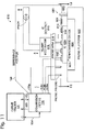
- FIG. 1 is a schematic block diagram of a curve tracer signal conversion device.
- FIG. 2 is a more detailed schematic block diagram of the curve tracer conversion device of FIG. 1 .
- FIG. 3 is a timing diagram depicting the relationship between the base signal sequence, the sequence of selection signals, the sequence of conversion device signal outputs (selected port measured electrical response), and the reset signal.
- FIG. 4 is a detailed schematic of an exemplary reset module.
- FIG. 5 is a detailed schematic of an exemplary selector module.
- FIG. 6 is a schematic block diagram of a universal socketless integrated circuit (IC) electrical test fixture.
- FIG. 7 is a plan view of the IC bottom surface showing m rows of IC contacts.
- FIG. 8 is a plan view showing a row of probe pins mounted on the probe arm.
- FIG. 9 is a diagram of a socketless IC contact connector.
- FIGS. 10A and 10B are detailed partial cross-sectional and plan views, respectively, of the connector loop engaged with an IC contact.
- FIG. 11 is a diagram depicting a universal socketless IC test fixture with a contact connector.
- FIG. 12 is a plan view of the IC bottom surface showing the connector engaging IC contact 110 z in row m of the IC contacts.
- FIG. 1 is a schematic block diagram of a curve tracer signal conversion device.
- the signal conversion device 100 comprises an input on line 102 connected to a curve tracer 101 base port to accept a repeating sequence of stepped base signals.
- the conversion device 100 has a signal input on line 104 connected to either the curve tracer collector or emitter ports, which is referred to herein as the “selected” port.
- the conversion device 100 has a plurality of signal outputs 106 , where each signal output is sequentially connected to the selected curve tracer port in response to a corresponding base step signal. Shown are signal output ports 106 a through 106 p , where p is a variable not limited to any particular value.
- the unselected e.g., emitter port
- the conversion device supplies the reference voltage to a unit under test on line 124 .
- FIG. 2 is a more detailed schematic block diagram of the curve tracer conversion device of FIG. 1 .
- a high pass filter 200 has an input connected to the curve tracer base port on line 102 , and an output on line 202 to supply a filtered sequence of stepped base signals.
- the high pass filter 200 comprises a series capacitor and a shunt resistor.
- the high pass filter 200 forms a differentiating circuit that responds (passes) to the faster transitions of each step change and the falling edge at the end of the group of steps. This response means that pulses are produced at the transitions, with no change in response to the DC level changes of the steps. That is, the signals on line 204 are AC pulses, with no DC component.
- a reset module 204 has an input connected to the high pass filter output on line 202 to accept the filtered repeating sequence of stepped base signals (AC pulses), and an output on line 206 to supply a reset trigger following each sequence.
- a selector module 208 has an input connected to the high pass filter output on line 202 to accept the filtered repeating sequence of stepped base signals.
- the selector module has an output on line 210 to supply a sequence of selection signals in response to the corresponding sequence of stepped base signals.
- a counter 212 has a reset input on line 206 to accept the reset trigger and a clock input on line 210 to accept the selection signal.
- the counter 212 has a plurality of parallel outputs 214 ; outputs 214 a through 214 p are shown. Each output 214 is enabled in sequence in response to the corresponding sequence of selection signals. The sequence of outputs is reset to an initial output in response to the reset trigger.
- the conversion device 100 also comprises a network of parallel switches 216 .
- Switches 216 a through 216 p are shown.
- Each switch 216 has a signal input connected to the curve tracer selected port.
- the switch signal inputs may be connected to the collector port.
- Each switch 216 has a control input on line 218 , and a signal output connected to a signal conversion device output on line 106 .
- gating transistors 220 a through 220 p are interposed between the switches 216 and the counter outputs on line 214 .
- Each transistor 220 has a base connected to a corresponding counter output on line 214 , a collector connected to a corresponding switch control input on line 218 , and an emitter connected to the unselected curve tracer port on line 108 .
- a reference voltage port is connected to the unselected curve tracer port on line 108 , to supply a reference voltage 124 .
- FIG. 3 is a timing diagram depicting the relationship between the base signal sequence, the sequence of selection signals, the sequence of conversion device signal outputs (selected port measured electrical response), and the reset signal.
- FIG. 4 is a detailed schematic of an exemplary reset module.
- the reset module 204 comprises a first resistor 400 having a first end connected the reset module input on line 202 and a second end connected to a first reference voltage on line 402 .
- the first reference voltage can be ground.
- a first diode 404 has an anode connected to the reset module input on line 202 , and a cathode. In one aspect not shown, the diode is a transistor with a floating collector.
- a second diode 406 has an anode connected to the first diode 404 cathode, and a cathode.
- An N channel JFET 408 has a gate connected to the second diode cathode, a source connected to the first reference voltage on line 402 , and a drain connected to the counter reset input on line 206 .
- a second resistor 410 has a first end connected to the JFET drain, and a second end connected to a second reference voltage on line 412 .
- the second reference voltage has a higher potential that the first reference voltage. It should be understood that a practitioner versed in the art would be able to enable the same functionality using an alternate collections of parts and voltages.
- FIG. 5 is a detailed schematic of an exemplary selector module.
- a first resistor 500 has a first end connected to the selector module input on line 202 , and a second end.
- a first npn transistor 502 has a base connected to the first resistor second end, a collector connected to the second reference voltage on line 412 , and an emitter.
- a second npn transistor 504 has a base connected to the first npn transistor 502 emitter, an emitter connected to the first reference voltage on line 402 , and a collector.
- a second resistor 506 has a first end connected to the second npn transistor 504 collector, and a second end connected to the second reference voltage on line 412 .
- a third npn transistor 508 has a base connected to the second npn transistor 506 collector, an emitter connected to the first reference voltage on line 402 , and a collector connected to the clock input of the counter on line 210 .
- a third resistor 510 has a first end connected to the third npn transistor 508 collector, and a second end connected to the second reference voltage on line 412 . It should be understood that a practitioner versed in the art would be able to enable the same functionality using an alternate collections of parts and voltages.
- FIG. 6 is a schematic block diagram of a universal socketless integrated circuit (IC) electrical test fixture.
- the test fixture 600 comprises a probing platform 602 to accept an IC 604 .
- the probe platform 602 is part of a heat sink, or includes a temperature chuck 606 to accept a top surface 608 of the IC 604 .
- the temperature of the chuck 606 can be controlled to support environmental temperature testing of the IC 104 .
- the IC 604 has electrical contacts 610 formed on a bottom surface 612 in an array of m rows, where each row includes n, or less contacts.
- a probe arm 614 includes p probe pins 616 , where p is typically greater than, or equal to n.
- a spring-loaded pogo pin is one example of a probe pin.
- n, m, and v are variables not limited to any particular value. When p is less than n, the probe arm position must be changed more often, if each IC contact is to be tested.
- the test fixture 600 comprises the curve tracer 101 with base, collector, and emitter ports.
- the test fixture 600 further comprises the curve tracer signal conversion device 100 .
- the conversion device 100 has an input connected to the curve tracer 101 base port on line 102 to accept a repeating sequence of stepped base signals, a signal input connected to the curve tracer selected port (e.g., collector port) on line 104 , and p signal outputs on line 106 ( 106 a - 106 p ), where each signal output 106 is connected to a corresponding probe pin 616 .
- the probe pins 616 are sequentially connected to the selected curve tracer port in response to a corresponding base step signal. Details of the curve tracer conversion device are presented above in the explanation of FIGS. 2 through 5 .
- FIG. 7 is a plan view of the IC bottom surface showing m rows of IC contacts. In row 1 , contacts 610 a through 610 n are shown, with a spacing 700 between contacts.
- FIG. 8 is a plan view showing a row of probe pins 616 mounted on the probe arm 614 .
- the spacing 702 between the probe pins 616 about matches the spacing between IC contacts (see FIG. 7 ).
- the p probe pins are mounted in the probe arm in a straight row.
- other probe pin mounting arrangements would be possible.
- a clamping mechanism 618 is used to mechanically interface the probe arm probe pins 616 to a row of n IC contacts 610 under test.
- a number of suitable mechanisms can be adapted for this purpose, and the test fixture is not limited to any particular one.
- the curve tracer selected port on line 104 is selectively connected to the p probe pins 616 of the probe arm to measure electrical characteristics associated with the IC contacts 610 under test. Some examples of electrical characteristics include current, voltage, real and imaginary impedances, and delay.
- the probe arm 614 , clamping mechanism 618 , and probe platform 602 work in cooperation to electrically interface any row of the IC contacts with the electrical measurement device. That is, the clamping mechanism can be engaged and disengaged to so that each row of IC contacts can be tested in sequence.
- the test fixture is not limited to testing an IC with any particular array pattern. Typically, the spacing between the IC contacts approximately matches the spacing between probe pins.
- the probe arm 614 , clamping mechanism 618 , and probe platform 602 work in cooperation to automatically electrically interface every row of the IC contacts with the electrical measurement device, in succession. For example, the test fixture initially connects the probe arm to row 1 of IC contacts, and after completing testing, releases. After moving the probe arm or probe platform, the probe is applied to row 2 of the IC contacts. In that manner, the rows of IC contacts are tested in succession.
- the curve tracer 101 supplies a reference voltage (the unselected port), via the interface on line 124 , to one of the IC contacts under test, so that the electrical characteristics of the IC contacts under test are measured with respect to the reference voltage.
- the reference voltage interface supplies both a ground and a power supply voltage, or a plurality of power supply voltages. In this case, at least one of the reference voltages is supplied by a source that is not the curve tracer.
- a second probe arm (not shown) may be used as the second interface to supply the reference voltage.
- the second probe may have p probe pins.
- the movement of the second probe may be independent of the first probe arm. That is, the second probe arm may be connected to any row of IC contacts, independent of row connected to the first probe arm.
- a second probe arm may be associated with a switching mechanism, so that a variety of different reference voltages may be switched to a particular IC contact (probe pin), or so that a reference voltage may be selectively supplied to different IC contacts (probe pins) interfaced to the second probe arm.
- a curve tracer can measure transistor collector electrical characteristics at a number of different base currents (voltages). Typically, the base current (voltage) is stepped, and the collector current (voltage) is measured at each step. As adapted for use with the test fixture of FIG. 6 , each time the curve tracer “steps” to a new base current (voltage), a different signal input on line 106 is selected. Thus, for each base step, the curve tracer collector port measures electrical characteristics associated with a unique IC contact.
- a further advantage to using the curve tracer base port to control the external switching is the simultaneous storage of the measurement in the curve tracer memory.
- Most digital curve tracers have internal memory storage capability. The memory storage is synchronized with the step waveform on the base port.
- the external measurement on the collector or emitter port is synchronized with the base port signal, and kept in a curve tracer internal memory. The external measurement can be recalled in response to referencing the base port voltage (switch control signal), which in turn, can be referenced to a particular IC contact.
- FIG. 9 is a diagram of a socketless IC contact connector.
- the connector 800 comprises an electrically conductive support post 802 .
- An electrically conductive spring 804 has a first end 806 connected to the post 802 , and a second end 808 .
- An electrically conductive first wire 810 has a first end 812 connected to the spring second end 808 , and a second end 814 .
- An electrically conductive loop 816 has a loop neck 818 connected to the first wire second end 814 .
- the loop 816 is formed by looping the first wire second end 814 .
- the loop may be a separate element connected (e.g., soldered) to the first wire.
- the first wire 810 doubles-back on itself after forming the loop 816 , so that the wire head and tail are both connected to the spring second end 808 .
- the spring 804 and loop 816 work in cooperation to engage an IC contact.
- an electrical insulating sleeve 822 overlies the first wire 810 .
- FIGS. 10A and 10B are detailed partial cross-sectional and plan views, respectively, of the connector loop engaged with an IC contact.
- the IC contact is a ball grid array (BGA) IC contact.
- the connector can be adapted to interface with any style contact.
- the loop 816 has a diameter 822 greater than the engaged BGA IC contact diameter 824 , so the loop can be slipped over the top 826 of the BGA, past the BGA maximum diameter 824 .
- the loop 816 is a wire having a wire diameter 828 less than the BGA diameter 824 . The smaller wire diameter permits to loop to remain engaged to the BGA contact as the loop is put under tension by the spring.
- the loop diameter 822 is in a range between 10 and 30 mils.
- a first wire or loop diameter of about 6 mils permits a secure engagement to any BGA contact in the above-mentioned range, however, other diameters will also enable the connector.
- a second wire 830 has a first end 832 connected to the spring second end 808 , and a second end 832 connected to the post 802 .
- the second wire 830 is useful in circumstances where the electrical resistance of the spring is relatively high.
- the spring 804 has a first electrical resistance and the second wire 830 has a second electrical resistance less than the first resistance.
- the spring 804 has an extension length 834 when the loop is engaged with the IC contact 820 .
- the second wire 830 has a length 836 greater than the spring extension length. Alternately, the second wire length 836 is selected to prevent the spring from being over-extended.
- FIG. 11 is a diagram depicting a universal socketless IC test fixture with a contact connector. The details of the test fixture have been described above and depicted in FIGS. 1-6 , and will not be repeated here in the interest of brevity.
- the test fixture 600 includes probing platform 602 to accept an IC 604 , where the IC 604 has electrical contacts 610 formed on a bottom surface 612 in an array of m rows, where each row includes n, or less contacts.
- a probe arm 114 includes p probe pins 616 , where p is greater than, or equal to n.
- a clamping mechanism 618 mechanically interfaces the probe arm probe pins 616 to a row of n IC contacts 610 under test.
- this aspect of the test fixture includes the IC contact connector 800 described above and depicted in FIGS. 9 , 10 A, and 10 B. Again, in the interest of brevity, only the basic elements of the connector are highlighted. However, it should be understood that connector of FIG. 11 may include all the aspects and variations mentioned above in the description of FIGS. 9 , 10 A, and 10 B.
- the connector 800 has an electrically conductive support post 800 .
- An electrically conductive spring 804 has a first end connected to the post 802 , and a second end.
- An electrically conductive first wire 810 having a first end connected to the spring second end, and a second end.
- An electrically conductive loop 816 with a loop neck is connected to the first wire second end.
- the wire ends, springs ends, and loop neck are explicitly labeled in FIG. 9 .
- the probe arm 614 , clamping mechanism 618 , and probe platform 602 work in cooperation to electrically interface a first row of IC contacts.
- the spring 804 and loop 816 work in cooperation to engage a single IC contact 610 in a second row of IC contacts. As shown, IC contact 610 z in engaged.
- the post 802 is connected to the reference voltage on line 124 to enable electrical testing.
- the post 802 can be connected to the emitter port of a curve tracer through conversion device 100 .
- the post 802 is shown mounted on the probe platform, but alternately, the post need not be mechanically interfaced to the probe platform.
- only a single connector 800 is shown, more than one connector may be used.
- one connector may be interfaced to an IC contact to power the IC, while another connector is connected to an IC ground.
- FIG. 12 is a plan view of the IC bottom surface 612 showing the connector 800 engaging IC contact 610 z in row m of the IC contacts.
- test fixture makes electrical connections directly to the pins of a package device, using one row of probe pins attached to a probing arm.
- the probe arm is assembled with the probe pins spacing being the same as that of the package pin pitch.
- Each row of device pins (contacts) is measured by sequentially stepping the row of probe pins across consecutive rows of package pins. Parametric measurements such as curve tracer analysis may be conducted on each probed pin.
- the test fixture eliminates the need for sockets and interface boards and permits real-time viewing of the device curves. Further, since the device under test is upside-down (pins up), the probe platform may be a temperature controlled chuck, which permits measurements to be made over temperature.
- a universal socketless test fixture, associated IC contact connector, and associated curve tracer conversion device have been provided. Examples of waveforms and hardware implementations have been given to illustrate the invention. However the invention is not limited to merely these examples. Other variations and embodiments of the invention will occur to those skilled in the art.
Abstract
Description
Claims (18)
Priority Applications (1)
| Application Number | Priority Date | Filing Date | Title |
|---|---|---|---|
| US12/551,524 US8188760B2 (en) | 2009-08-04 | 2009-08-31 | Curve tracer signal conversion for integrated circuit testing |
Applications Claiming Priority (3)
| Application Number | Priority Date | Filing Date | Title |
|---|---|---|---|
| US12/535,533 US7768283B1 (en) | 2009-08-04 | 2009-08-04 | Universal socketless test fixture |
| US12/541,058 US8106671B2 (en) | 2009-08-04 | 2009-08-13 | Socketless integrated circuit contact connector |
| US12/551,524 US8188760B2 (en) | 2009-08-04 | 2009-08-31 | Curve tracer signal conversion for integrated circuit testing |
Related Parent Applications (1)
| Application Number | Title | Priority Date | Filing Date |
|---|---|---|---|
| US12/541,058 Continuation-In-Part US8106671B2 (en) | 2009-08-04 | 2009-08-13 | Socketless integrated circuit contact connector |
Publications (2)
| Publication Number | Publication Date |
|---|---|
| US20110031993A1 US20110031993A1 (en) | 2011-02-10 |
| US8188760B2 true US8188760B2 (en) | 2012-05-29 |
Family
ID=43534354
Family Applications (1)
| Application Number | Title | Priority Date | Filing Date |
|---|---|---|---|
| US12/551,524 Expired - Fee Related US8188760B2 (en) | 2009-08-04 | 2009-08-31 | Curve tracer signal conversion for integrated circuit testing |
Country Status (1)
| Country | Link |
|---|---|
| US (1) | US8188760B2 (en) |
Cited By (1)
| Publication number | Priority date | Publication date | Assignee | Title |
|---|---|---|---|---|
| US10460326B2 (en) | 2017-10-24 | 2019-10-29 | Global Circuit Innovations, Inc. | Counterfeit integrated circuit detection by comparing integrated circuit signature to reference signature |
Families Citing this family (3)
| Publication number | Priority date | Publication date | Assignee | Title |
|---|---|---|---|---|
| US9939488B2 (en) * | 2011-08-31 | 2018-04-10 | Teseda Corporation | Field triage of EOS failures in semiconductor devices |
| US20140266290A1 (en) * | 2013-03-14 | 2014-09-18 | Bhavin Odedara | Process detection circuit |
| CN104502786A (en) * | 2015-01-05 | 2015-04-08 | 苏州路之遥科技股份有限公司 | Multi-insertion-rod multi-insertion-method wiring harness intelligent test machine automatic recognition system |
Citations (9)
| Publication number | Priority date | Publication date | Assignee | Title |
|---|---|---|---|---|
| US5722159A (en) * | 1994-03-30 | 1998-03-03 | International Business Machines Corporation | Method for retention of a fragile conductive trace with a protective clamp |
| US5777487A (en) * | 1996-05-02 | 1998-07-07 | Burgess; David L. | Method for detecting failures in electric circuits and tester, liquid crystal for use therewith |
| US6246250B1 (en) * | 1998-05-11 | 2001-06-12 | Micron Technology, Inc. | Probe card having on-board multiplex circuitry for expanding tester resources |
| US20030038365A1 (en) * | 2001-08-22 | 2003-02-27 | Farnworth Warren M. | Substrate mapping |
| US7091733B2 (en) * | 2001-11-30 | 2006-08-15 | Tokyo Electron Limited | Reliability evaluation test apparatus, reliability evaluation test system, contactor, and reliability evaluation test method |
| US7272760B2 (en) * | 2004-11-18 | 2007-09-18 | Systems On Silicon Manufacturing Co. Pte. Ltd. | Curve tracing device and method |
| US7355426B2 (en) * | 2003-01-14 | 2008-04-08 | Infineon Technologies Ag | Universal measuring adapter system |
| US7768283B1 (en) * | 2009-08-04 | 2010-08-03 | Applied Micro Circuits Corporation | Universal socketless test fixture |
| US8106671B2 (en) * | 2009-08-04 | 2012-01-31 | Applied Micro Circuits Corporation | Socketless integrated circuit contact connector |
-
2009
- 2009-08-31 US US12/551,524 patent/US8188760B2/en not_active Expired - Fee Related
Patent Citations (9)
| Publication number | Priority date | Publication date | Assignee | Title |
|---|---|---|---|---|
| US5722159A (en) * | 1994-03-30 | 1998-03-03 | International Business Machines Corporation | Method for retention of a fragile conductive trace with a protective clamp |
| US5777487A (en) * | 1996-05-02 | 1998-07-07 | Burgess; David L. | Method for detecting failures in electric circuits and tester, liquid crystal for use therewith |
| US6246250B1 (en) * | 1998-05-11 | 2001-06-12 | Micron Technology, Inc. | Probe card having on-board multiplex circuitry for expanding tester resources |
| US20030038365A1 (en) * | 2001-08-22 | 2003-02-27 | Farnworth Warren M. | Substrate mapping |
| US7091733B2 (en) * | 2001-11-30 | 2006-08-15 | Tokyo Electron Limited | Reliability evaluation test apparatus, reliability evaluation test system, contactor, and reliability evaluation test method |
| US7355426B2 (en) * | 2003-01-14 | 2008-04-08 | Infineon Technologies Ag | Universal measuring adapter system |
| US7272760B2 (en) * | 2004-11-18 | 2007-09-18 | Systems On Silicon Manufacturing Co. Pte. Ltd. | Curve tracing device and method |
| US7768283B1 (en) * | 2009-08-04 | 2010-08-03 | Applied Micro Circuits Corporation | Universal socketless test fixture |
| US8106671B2 (en) * | 2009-08-04 | 2012-01-31 | Applied Micro Circuits Corporation | Socketless integrated circuit contact connector |
Cited By (1)
| Publication number | Priority date | Publication date | Assignee | Title |
|---|---|---|---|---|
| US10460326B2 (en) | 2017-10-24 | 2019-10-29 | Global Circuit Innovations, Inc. | Counterfeit integrated circuit detection by comparing integrated circuit signature to reference signature |
Also Published As
| Publication number | Publication date |
|---|---|
| US20110031993A1 (en) | 2011-02-10 |
Similar Documents
| Publication | Publication Date | Title |
|---|---|---|
| US5519331A (en) | Removable biasing board for automated testing of integrated circuits | |
| KR101293381B1 (en) | A method and apparatus for increasing the operating frequency of a system for testing electronic devices | |
| US4862076A (en) | Test point adapter for chip carrier sockets | |
| US8106671B2 (en) | Socketless integrated circuit contact connector | |
| US20060082358A1 (en) | Interface apparatus for semiconductor device tester | |
| US7768283B1 (en) | Universal socketless test fixture | |
| US5825171A (en) | Universal burn-in board | |
| US8188760B2 (en) | Curve tracer signal conversion for integrated circuit testing | |
| KR100717672B1 (en) | Zig substrate for testing sensor, testing apparatus and testing method of the same | |
| KR100478261B1 (en) | Semiconductor substrate testing apparatus | |
| US20090128172A1 (en) | Calibration board for electronic device test apparatus | |
| US8278955B2 (en) | Test interconnect | |
| JP2737774B2 (en) | Wafer tester | |
| US6507205B1 (en) | Load board with matrix card for interfacing to test device | |
| JPH0348171A (en) | Leadless probe card of in-circuit tester for hybrid integrated circuit | |
| CN215415737U (en) | PCB board test point testing arrangement | |
| CN216718593U (en) | Integrated circuit sorting machine and sorting system | |
| JPH0540131A (en) | Testing jig | |
| CA1273130A (en) | Test point adapter for chip carrier sockets | |
| JPH0720193A (en) | Dut board | |
| JP2011220859A (en) | Method for testing semiconductor devices | |
| JP2926759B2 (en) | Semiconductor integrated circuit measurement jig | |
| JPH0587875A (en) | Shift probe tyupe in-circuit tester | |
| JP2019086359A (en) | Semiconductor device manufacturing method | |
| US20160377652A1 (en) | Semiconductor device manufacturing method |
Legal Events
| Date | Code | Title | Description |
|---|---|---|---|
| AS | Assignment |
Owner name: APPLIED MICRO CIRCUITS CORPORATION, CALIFORNIA Free format text: ASSIGNMENT OF ASSIGNORS INTEREST;ASSIGNOR:PATTERSON, JOSEPH;REEL/FRAME:023174/0009 Effective date: 20090831 |
|
| STCF | Information on status: patent grant |
Free format text: PATENTED CASE |
|
| FPAY | Fee payment |
Year of fee payment: 4 |
|
| FEPP | Fee payment procedure |
Free format text: PAYOR NUMBER ASSIGNED (ORIGINAL EVENT CODE: ASPN); ENTITY STATUS OF PATENT OWNER: LARGE ENTITY |
|
| AS | Assignment |
Owner name: MACOM CONNECTIVITY SOLUTIONS, LLC, MASSACHUSETTS Free format text: MERGER AND CHANGE OF NAME;ASSIGNORS:APPLIED MICRO CIRCUITS CORPORATION;MACOM CONNECTIVITY SOLUTIONS, LLC;REEL/FRAME:042423/0700 Effective date: 20170126 |
|
| AS | Assignment |
Owner name: GOLDMAN SACHS BANK USA, AS COLLATERAL AGENT, NEW Y Free format text: SECURITY INTEREST;ASSIGNOR:MACOM CONNECTIVITY SOLUTIONS, LLC (SUCCESSOR TO APPLIED MICRO CIRCUITS CORPORATION);REEL/FRAME:042444/0891 Effective date: 20170504 Owner name: GOLDMAN SACHS BANK USA, AS COLLATERAL AGENT, NEW YORK Free format text: SECURITY INTEREST;ASSIGNOR:MACOM CONNECTIVITY SOLUTIONS, LLC (SUCCESSOR TO APPLIED MICRO CIRCUITS CORPORATION);REEL/FRAME:042444/0891 Effective date: 20170504 |
|
| FEPP | Fee payment procedure |
Free format text: MAINTENANCE FEE REMINDER MAILED (ORIGINAL EVENT CODE: REM.); ENTITY STATUS OF PATENT OWNER: LARGE ENTITY |
|
| LAPS | Lapse for failure to pay maintenance fees |
Free format text: PATENT EXPIRED FOR FAILURE TO PAY MAINTENANCE FEES (ORIGINAL EVENT CODE: EXP.); ENTITY STATUS OF PATENT OWNER: LARGE ENTITY |
|
| STCH | Information on status: patent discontinuation |
Free format text: PATENT EXPIRED DUE TO NONPAYMENT OF MAINTENANCE FEES UNDER 37 CFR 1.362 |
|
| FP | Lapsed due to failure to pay maintenance fee |
Effective date: 20200529 |