US8183906B2 - Arrangement, use of an arrangement, reference voltage source and method for generating a voltage value linearly proportional to the temperature - Google Patents
Arrangement, use of an arrangement, reference voltage source and method for generating a voltage value linearly proportional to the temperature Download PDFInfo
- Publication number
- US8183906B2 US8183906B2 US12/403,837 US40383709A US8183906B2 US 8183906 B2 US8183906 B2 US 8183906B2 US 40383709 A US40383709 A US 40383709A US 8183906 B2 US8183906 B2 US 8183906B2
- Authority
- US
- United States
- Prior art keywords
- unit
- voltage value
- input
- output
- logarithmizing
- Prior art date
- Legal status (The legal status is an assumption and is not a legal conclusion. Google has not performed a legal analysis and makes no representation as to the accuracy of the status listed.)
- Active
Links
- 238000000034 method Methods 0.000 title claims description 45
- 239000004065 semiconductor Substances 0.000 claims description 77
- 230000001419 dependent effect Effects 0.000 claims description 13
- 238000011156 evaluation Methods 0.000 claims description 12
- 230000005669 field effect Effects 0.000 claims description 11
- 238000004364 calculation method Methods 0.000 claims description 4
- 230000008569 process Effects 0.000 description 5
- 230000004069 differentiation Effects 0.000 description 4
- 230000015572 biosynthetic process Effects 0.000 description 3
- 238000010079 rubber tapping Methods 0.000 description 3
- 238000011161 development Methods 0.000 description 2
- 238000005516 engineering process Methods 0.000 description 2
- 230000006641 stabilisation Effects 0.000 description 2
- 238000011105 stabilization Methods 0.000 description 2
- 230000001629 suppression Effects 0.000 description 2
- 239000000654 additive Substances 0.000 description 1
- 230000000996 additive effect Effects 0.000 description 1
- 238000009529 body temperature measurement Methods 0.000 description 1
- 239000003990 capacitor Substances 0.000 description 1
- 230000008859 change Effects 0.000 description 1
- 239000000470 constituent Substances 0.000 description 1
- 238000010276 construction Methods 0.000 description 1
- 238000013461 design Methods 0.000 description 1
- 238000001514 detection method Methods 0.000 description 1
- 238000010586 diagram Methods 0.000 description 1
- 238000004519 manufacturing process Methods 0.000 description 1
- 239000002184 metal Substances 0.000 description 1
- 230000004044 response Effects 0.000 description 1
- 238000005070 sampling Methods 0.000 description 1
- 238000012546 transfer Methods 0.000 description 1
Images


Classifications
-
- G—PHYSICS
- G01—MEASURING; TESTING
- G01K—MEASURING TEMPERATURE; MEASURING QUANTITY OF HEAT; THERMALLY-SENSITIVE ELEMENTS NOT OTHERWISE PROVIDED FOR
- G01K7/00—Measuring temperature based on the use of electric or magnetic elements directly sensitive to heat ; Power supply therefor, e.g. using thermoelectric elements
- G01K7/01—Measuring temperature based on the use of electric or magnetic elements directly sensitive to heat ; Power supply therefor, e.g. using thermoelectric elements using semiconducting elements having PN junctions
Definitions
- the invention relates to an arrangement, use of an arrangement, reference voltage source and method for generating a voltage value linearly proportional to temperature, and particularly to an arrangement, use of an arrangement, reference voltage source and method for generating a voltage value linearly proportional to the temperature with a logarithmizing unit and a subtracting unit, wherein a voltage value can be tapped off at the output of the subtracting unit and said voltage value is linearly proportional to the temperature.
- Reference voltage sources which are very substantially independent of process fluctuations, fluctuations of the supply voltage and fluctuations of the ambient variables are required nowadays in integrated circuits.
- ambient variables that shall be mentioned here include temperature, pressure and the like.
- high-volume integrated circuits require temperature sensors which detect a value representing the ambient temperature in the circuit and, with the result of this detection, control corresponding compensation circuits or actively control the circuits.
- a multiplicity of circuits and circuit concepts have been disclosed heretofore.
- One known method for generating a reference value is the principle of compensating for fluctuations that are accumulated in the form of additive disturbance on a reference value. Temperature compensation is often carried out in this case.
- the reference values are determined in many cases by the prefactor k*T/e, where k is the Boltzmann constant, T is the temperature and e is the elementary charge.
- Temperature-sensitive components that shall be specified here include metal or semiconductor resistors, PN or tunnel junction of components or bipolar transistors. These conductivities of the components are not absolute quantities. They are subjected to the production tolerances and usually require calibration routines for an accurate temperature measurement. This usually involves a temperature sensor undergoing passes with known temperature cycles and the measured conductivity or the current value corresponding to the temperature being stored. These stored values are compared with the measured values later in order to reconstruct the actual temperature value. At low temperatures, the thermal noise is also used for measuring the temperature in special cases.
- each logarithmizing unit has an input and an output, is connected by the input to a first terminal of a voltage source, wherein the voltage source provides an input voltage and has a second terminal, which is connected to reference-ground potential, has a semiconductor component and has an operating point setting unit, wherein the operating point setting unit sets an operating point in the sub threshold voltage range of the input characteristic curve of the semiconductor component, and a subtracting unit, wherein the subtracting unit has a first input, a second input and also an output, wherein a respective one of the inputs of the subtracting unit is connected to one of the outputs of the logarithmizing units, and wherein a voltage value can be tapped off at the output of the subtracting unit and the voltage value is linearly proportional to the temperature.
- the use of the arrangement as a temperature sensor is provided, wherein the semiconductor component is a field effect transistor, an evaluation unit is connected downstream of the subtracting unit, the evaluation unit detects the voltage value that can be tapped off and determines the temperature by means of a calculation unit within the evaluation unit, wherein the voltage value that can be tapped off is dependent only on the depletion zone capacitances, the Boltzmann constant, the elementary charge and the natural logarithm of a resistance ratio within the logarithmizing unit.
- a reference voltage source with use of the arrangement is provided, wherein the temperature dependence of the voltage value that can be tapped off is compensated for.
- a method for generating a voltage value linearly proportional to the temperature by means of a semiconductor component comprising the following method steps: setting a first operating point in the sub threshold voltage range of the input characteristic curve of the semiconductor component, logarithmizing a temperature-dependent input voltage, using the semiconductor component, differentiating the logarithmic input voltage, and tapping off or providing the voltage value linearly proportional to the temperature.
- a method for generating a voltage value linearly proportional to the temperature by means of semiconductor components comprising the following method steps: setting a first operating point in the sub threshold voltage range of the input characteristic curve of a first semiconductor component, setting a second operating point in the sub threshold voltage range of the input characteristic curve of a second semiconductor component temporally in parallel with setting the first operating point, wherein the first operating point is not equal to the second operating point, logarithmizing a temperature-dependent input voltage, simultaneously using both semiconductor components, forming the difference between the two logarithmic input voltages, and tapping off or providing the voltage value linearly proportional to the temperature.
- a method for generating a voltage value linearly proportional to the temperature by means of a semiconductor component comprising the following method steps: setting a first operating point in the sub threshold voltage range of the input characteristic curve of the semiconductor component, logarithmizing a temperature-dependent input voltage, using the semiconductor component, buffer-storing the logarithmized input voltage, setting a second operating point in the sub threshold voltage range of the input characteristic curve of the semiconductor component, logarithmizing a temperature-dependent input voltage, using the semiconductor component with a changed operating point, buffer-storing the second logarithmized input voltage, forming the difference between the two logarithmized input voltages, tapping off or providing the voltage value linearly proportional to the temperature.
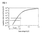
- FIG. 1 shows an input characteristic curve of a semiconductor component with a logarithmic representation of the drain current I D versus the gate voltage V g .
- FIG. 2 shows an exemplary embodiment of an arrangement for providing a voltage value that is linearly proportional to the temperature.
- FIG. 3 shows a development of the exemplary embodiment illustrated in FIG. 2 .
- FIG. 4 shows an alternative exemplary embodiment with regard to the exemplary embodiment illustrated in FIG. 1 .
- FIG. 5 shows a voltage-time diagram of a switching signal.
- FIG. 6 shows a semiconductor component
- FIG. 7 shows an alternative semiconductor component.
- FIG. 8 shows in a and b an alternative semiconductor component in different interconnection variants.
- FIG. 9 shows a subtracting unit
- FIG. 10 a shows an arrangement for generating a voltage reference.
- FIG. 10 b shows an alternative arrangement with respect to the arrangement illustrated in FIG. 10 a.
- FIG. 11 shows an exemplary embodiment for generating a temperature-independent voltage value.
- FIG. 12 shows a method flowchart for a method for generating a voltage value linearly proportional to the temperature.
- FIG. 13 shows a method flowchart for an alternative method for generating a voltage value linearly proportional to the temperature.
- FIG. 14 shows a method flowchart for an alternative method for generating a voltage value linearly proportional to the temperature.
- FIG. 1 An input characteristic curve of a semiconductor component 3 is indicated in FIG. 1 .
- the drain current I D through said semiconductor component 3 is represented logarithmically versus the gate voltage V g .
- the sub threshold voltage range V g,sub illustrated here extends from 0 volts to approximately 0.6 volt.
- the characteristic curve of the semiconductor component 3 can be regarded as virtually exponential in this range.
- the input characteristic curve of the semiconductor component 3 is a straight line in the range V g,sub .
- an NMOS field effect transistor as semiconductor component 3 was operated with a drain voltage of one volt.
- the NMOS field effect transistor has a gate width of 0.3 ⁇ m and a gate length of 0.25 ⁇ m.
- the characteristic curve in the sub threshold voltage range V g,sub can be described by the following formula: dV g /d ln( I D ) ⁇ ( k*T/e )*ln(10)*(1 +C d /C i ). If the semiconductor component 3 is a bipolar transistor, then the last term (1+C d /C i ) is omitted.
- dV g /d ln(I D ) is referred to as the inverse sub threshold slope.
- the inverse sub threshold slope is dependent on the Boltzmann constant k, the elementary charge e and the temperature T. Specifically in the case of a MOS transistor, an additional dependence on the depletion capacitance C d and the dielectric capacitance C i is also present.
- the following illustrations present arrangements and methods which utilize this exponential inverse sub threshold slope and provide a voltage value linearly proportional to the temperature.
- an input voltage V e is firstly logarithmized. This is followed by differentiation with respect to the gate voltage V g . After the differentiation, a voltage value V out linearly proportional to the temperature T can be tapped off.
- difference formation is carried out, which leads to the same result on account of the logarithmized exponential relationship between drain current I D and gate voltage V g .
- FIG. 2 presents an exemplary embodiment of an arrangement for generating a voltage value linearly proportional to the temperature.
- Two logarithmizing units 1 are provided for this purpose.
- the logarithmizing units 1 each have an input 101 and an output 102 .
- the two inputs 101 of the logarithmizing units 1 are connected to a first terminal 201 of a voltage source 2 .
- the voltage source 2 has a second terminal 202 , which is connected to a reference-ground potential GND.
- the voltage source 2 provides an input voltage V e .
- Each of the logarithmizing units 1 contains an operating point setting unit 4 and a semiconductor component 3 .
- the two outputs 102 of the logarithmizing units 1 are respectively connected to an input 501 , 502 of a subtracting unit 5 .
- the subtracting unit 5 additionally has an output 503 , at which a voltage value V out linearly proportional to a temperature T can be tapped off.
- the operating point setting unit 4 sets an operating point on the input characteristic curve of the semiconductor component 3 according to FIG. 1 , wherein the operating point lies in the sub threshold voltage range V g,sub of the semiconductor component 3 .
- a logarithmized sub threshold voltage value is available at the output 102 of the logarithmizing unit 1 .
- the two semiconductor components 3 are, in particular, of identical design. Transistors having an identical gate width and gate length are preferably used when a MOSFET transistor is used. Each operating point setting unit 4 sets a different operating point on the characteristic curve illustrated in FIG. 1 .
- FIG. 3 presents a development of the exemplary embodiment illustrated in FIG. 2 . Only the differences between FIG. 2 and FIG. 3 are discussed below.
- FIG. 3 essentially illustrates the logarithmizing unit 1 in greater detail.
- the operating point setting unit 4 and the semiconductor component 3 are shown in the logarithmizing unit 1 .
- the operating point setting unit 4 has an input 401 , which is connected to the input of the logarithmizing unit 101 .
- the output 402 of the operating point setting unit 4 is connected to a first terminal 301 of the semiconductor component 3 .
- the second terminal 302 of the semiconductor component 3 is in turn connected to the output 102 of the logarithmizing unit 1 .
- An operational amplifier 6 is disposed in parallel with the semiconductor component 3 .
- the operational amplifier 6 is connected by its negative input 602 to the first terminal 301 of the semiconductor component.
- the output 603 of the operational amplifier 6 is connected to the second terminal 302 of the semiconductor component 3 .
- the operational amplifier 6 has a positive input 601 .
- the positive input 601 of the operational amplifier 6 is connected to an integer multiple r of the input voltage V e of the voltage source 2 .
- the operating point setting unit 4 in this case is a non-reactive resistor having the value R.
- the second logarithmizing unit 1 which is connected to the second input 502 of the subtracting unit 5 , is constructed identically to the logarithmizing unit just described, with the only exception being that the operating point setting unit 4 has a resistance value amounting to n times the resistance value R. Consequently, each of the two operating point setting units 4 sets a different operating point in the sub threshold voltage range V g,sub of the semiconductor component 3 .
- High common-mode rejection and supply voltage suppression are produced owing to the use of an operational amplifier 6 in the logarithmizing unit 1 .
- the operational amplifier is connected up as a logarithmizer by the semiconductor component 3 being arranged in its feedback path.
- This stabilization is the fundamental task of the operational amplifier 6 .
- V ( k*T/e )*1 n ( V e )*( r ⁇ 1)/ I s *R is present at the output 603 of the operational amplifier 6 .
- a term (1+C d /C i ) is additionally inserted in the case where MOSFET transistors are used.
- I s describes a current that flows through the respective semiconductor component.
- V e is the input voltage V e of the voltage source 2 .
- n represents the ratio of the two resistances R, nR.
- the ratio should preferably be chosen such that the difference in the voltage drop is large in relation to process fluctuations but also small enough that a constant sub threshold voltage slope can be assumed.
- n typically lies between 4 and 16.
- FIG. 4 An alternative exemplary embodiment to FIG. 2 is presented in FIG. 4 .
- the logarithmizing unit 1 has an input 101 and an output 102 .
- the input 101 is in turn connected to the first potential 201 of the voltage source 2 .
- a changeover unit 8 is provided between logarithmizing unit 1 and subtracting unit 5 .
- the changeover unit 8 has two outputs, wherein each output is connected to in each case only one input 501 or 502 of the subtracting unit 5 .
- a voltage V out linearly proportional to the temperature can again be tapped off at the output 503 of the subtracting unit 5 .
- FIG. 4 An operational amplifier 6 , a semiconductor component 3 and an operating point setting unit 4 are once again shown in the logarithmizing unit 1 .
- the operating point setting unit 4 is embodied alternatively in FIG. 4 .
- the operating point setting unit 4 has an input 401 and an output 402 .
- Two resistors R and nR are provided in the operating point setting unit 4 .
- a switching element 7 is additionally inserted into the operating point setting unit 4 .
- Said switching element 7 has a first input 701 , which is connected to one terminal of the resistor R.
- a second input 702 of the switching element 7 is connected to the resistor nR.
- An output 703 of the switching element 7 is connected to the output 402 of the operating point setting unit 4 .
- the operating point setting unit 4 additionally has a control input 403 .
- the resistors R and nR are connected to one another by the respective other terminal and are connected to the input 401 of the operating point setting unit 4 .
- the changeover unit 8 likewise has a switching element 7 .
- This switching element 7 is identical to the switching element 7 of the operating point setting unit 4 .
- the switching element 7 in the changeover unit 8 is connected to the output 102 of the logarithmizing unit 1 .
- the first input 701 of the switching element is connected to a storage element 802 .
- the storage element 802 is in turn connected to the first input 501 of the subtracting unit 5 .
- the second input 702 is likewise connected to a further storage element 802 .
- the further storage element 802 is in turn connected to the second input 502 of the subtracting unit 5 .
- Both switching elements 7 have two switching states 704 , 705 . By means of a switching signal 706 , both switching elements 7 are switched from the first switching state 704 to the second switching state 705 , and vice versa.
- a corresponding switching signal ⁇ 1 is illustrated in FIG. 5 .
- a first switching state 704 of the switching signal 706 is, for example, a high state of a digital signal and the second switching state 705 is the low state of the switching signal 706 .
- FIG. 4 In contrast to FIG. 2 , only one logarithmizing unit is necessary in FIG. 4 .
- the operating point setting unit 4 By means of the operating point setting unit 4 , firstly a first operating point of the semiconductor element 3 is set by the first switching state 704 of the switching element 7 . Since both switching elements 7 in each case always have the same switching state, the output of the logarithmizing unit 102 is firstly combined with the first input 501 via the storage element 802 .
- the storage element 802 is a capacitor, for example, which is connected to reference-ground potential GND.
- each switching element 7 is switched from the first switching state 704 to the second switching state 705 by means of the switching signal 706 .
- the resistor nR in the operating point setting unit 4 is connected to the negative input 602 of the logarithmizing operational amplifier 6 .
- a second operating point which is different than the first operating point, is set in the semiconductor component 3 .
- the output voltage value at the output 102 of the logarithmizing unit 1 is stored in the further storage element 802 .
- the subtracting unit subtracts the two stored values of the storage elements 802 and provides the voltage V out at the output 503 .
- the switching elements 7 change their state, whereby different operating points are set in the sub threshold voltage range of the semiconductor component 3 .
- the exemplary embodiment according to FIG. 4 requires less space.
- FIGS. 6 , 7 , 8 a and 8 b each present alternative exemplary embodiments of semiconductor components 3 .
- FIG. 6 illustrates an NMOSFET transistor 9 .
- the latter is connected up as a diode, that is to say that the gate terminal 901 of the transistor 9 is connected to the source terminal 903 .
- the drain terminal 902 corresponds to the second terminal 302 of the semiconductor component 3
- the source terminal 903 corresponds to the first terminal 301 of the semiconductor component 3 .
- the voltage V out that can be tapped off is additionally dependent on the capacitance of the depletion zone C d and the dielectric capacitance C i .
- the circuit can likewise be realized with a PMOSFET transistor.
- the capacitance of the depletion zone C d is process-independent in all cases.
- Long-channel transistors or transistors having a long-channel behavior should ideally be used.
- a semiconductor component 3 is referred to as long-channel if its gate length is higher by a multiple, for example ten, then the minimum gate length that can be used in the technology.
- the corresponding gate length of the transistor 9 should be ten times greater than the minimum gate length available in the respective technology.
- FIG. 7 illustrates an alternative semiconductor component.
- a diode 10 as semiconductor component 3 in this case has an anode terminal 110 corresponding to the first terminal 301 of the semiconductor component 3 .
- the cathode terminal 111 is the second terminal 302 of the semiconductor component 3 .
- FIG. 8 a An alternative semiconductor component 3 is presented in FIG. 8 a .
- a bipolar transistor 11 is used in this case, the base terminal 114 of said bipolar transistor being connected to reference-ground potential GND.
- the emitter terminal 112 corresponds to the second terminal 302 of the semiconductor component 3 .
- the collector terminal 113 of the bipolar transistor 11 is identical with the first terminal 301 of the semiconductor component 3 .
- the depletion zone capacitance C d and the dielectric capacitance C i are not included as parameters of the voltage value V out that can be tapped off.
- FIG. 8 b The same semiconductor component 3 as in FIG. 8 a is used in FIG. 8 b .
- the base terminal 114 is not connected to reference-ground potential GND, but rather to the collector terminal 113 .
- FIG. 9 illustrates a subtracting unit 5 in greater detail.
- the operational amplifier variant should preferably be used. A description at this juncture can be omitted since the circuit is known from the prior art.
- the figures that have been represented up to this point present an arrangement corresponding to a linear temperature sensor that is dependent only on physical constants k, e and a constant divider ratio n.
- the capacitance of the depletion zone C d and the dielectric capacitance C i are also present as parameters. If the voltage V out is tapped off and acquired, the temperature can be deduced in a simple manner. This is done primarily in an evaluation unit connected downstream of the subtracting unit.
- the evaluation unit preferably has a calculation unit, which implements the known formula and supplies a current temperature value T.
- the evaluation unit can be embodied in terms of hardware or else software technology. Consequently, this circuit is suitable as an absolute and linear temperature sensor which thus covers a relatively large temperature range.
- the construction with operational amplifiers 6 additionally makes it possible to obtain a high degree of suppression of disturbing influences as a result of supply voltage fluctuations.
- FIGS. 10 a and 10 b are taken from the prior art. They provide a further reference V T,ref having a negative temperature coefficient. The description of FIGS. 10 a and 10 b is dispensed with at this juncture.
- V T,ref as output voltage of the arrangement from FIG. 10 a corresponds approximately to the threshold voltage value V th,T1 of the transistor T 1 as a function of the temperature.
- V T,ref ⁇ V th,T1 ( T 1) ⁇ V th,T1 ( T 0 )*( T 0 /T ⁇ 1).
- V th,T1 is the threshold voltage of the transistor T 1 and T 0 is room temperature, that is to say approximately 300 Kelvin.
- FIG. 11 indicates an exemplary embodiment of an arrangement which supplies a temperature-independent voltage reference VT,out as output voltage.
- the subtracting unit 5 is embodied in the manner illustrated in FIG. 9 .
- a further branching is provided at the positive input 901 of the operational amplifier 9 of the subtracting unit 5 , a series circuit composed of an a-fold non-reactive resistance and the unit 12 illustrated in FIG. 10 a being connected to said further branching.
- the temperature compensation is achieved by means of the resistance aR.
- a temperature-compensated voltage source can likewise be produced for the circuit from FIG. 10 a by a Taylor series expansion of the equation for V T,ref .
- the divider ratios a and b of the resistance values aR, bR should be chosen such that the temperature dependence ⁇ Vref is precisely compensated for.
- a temperature-independent voltage reference according to FIG. 10 b can also be produced analogously in this way.
- a simple temperature sensor accurate to a few degrees can likewise be used for generating V T,ref .
- the corresponding accuracy is obtained by the arrangement according to FIG. 11 .
- Offset compensation methods are also conceivable in addition to the fundamental representations of the operational amplifier circuit. Errors in the transfer functions are thereby minimized by offset voltages. Auto-calibrating methods should primarily be used for this purpose. Such methods are referred to as correlating double sampling CDS or chopper stabilization. In the CDS method, an assessment is not performed in absolute terms, but rather relative to a reference value.
- the voltage of the voltage references and thus also the temperatures thereof can be inverted by a suitable circuit or provided with quadratic terms.
- the temperature accuracy of the voltage reference can thus be increased.
- FIG. 12 illustrates a method flowchart for a method for generating a voltage value linearly proportional to the temperature.
- the method comprises a first step 14 , which involves setting a first operating point in the sub threshold voltage range of a semiconductor component 3 .
- a further step 15 involves logarithmizing the input voltage V e with the aid of this set semiconductor component 3 .
- the subsequent step 16 involves differentiating the logarithmized voltage value at the operating point with respect to the gate voltage V g .
- method step 17 involves providing a voltage linearly proportional to the temperature T.
- step 18 involves setting a first operating point in the sub threshold voltage range of the input characteristic curve of the semiconductor component, temporally in parallel with a second operating point in the sub threshold voltage range of the input characteristic curve of a further semiconductor component 3 .
- step 15 in which the input voltage V e is logarithmized simultaneously with the aid of the semiconductor components 3 in the logarithmizing unit 1 . Accordingly, two different logarithmized input voltage values are available.
- method step 19 involves forming the difference between the two logarithmized input voltage values.
- the subsequent method step 17 involves providing a voltage value linearly proportional to the temperature.
- step 14 involves setting a first operating point in the sub threshold voltage range of the input characteristic curve of the semiconductor component 3
- step 15 involves logarithmizing the input voltage value V e with the aid of the set semiconductor component 3
- subsequent step 20 involves buffer-storing the logarithmized voltage value.
- step 21 involves setting a second operating point in the sub threshold voltage range of the input characteristic curve of the semiconductor component. This is followed by logarithmizing the input voltage value V e with the aid of the newly set semiconductor component 3 in method step 15 .
- Step 20 involves buffer-storing the second logarithmized input voltage value.
- Step 19 then involves forming the difference between the two logarithmic voltage values.
- method step 17 in turn provides for providing a voltage value linearly proportional to the temperature.
Abstract
Description
dV g /d ln(I D)−(k*T/e)*ln(10)*(1+C d /C i).
If the
V=(k*T/e)*1n(V e)*(r−1)/I s *R
is present at the
ΔV=k*T/e*1n(n)
results at the
V T,ref ≈V th,T1(T1)≈V th,T1(T 0)*(T 0 /T−1).
In this case, Vth,T1 is the threshold voltage of the transistor T1 and T0 is room temperature, that is to say approximately 300 Kelvin.
- 1 Logarithmizing unit
- 101 Input of the logarithmizing unit
- 102 Output of the logarithmizing unit
- 2 Voltage source
- 201 First potential of the voltage source
- 202 Second potential of the voltage source
- 3 Semiconductor component
- 301 First terminal of the
semiconductor component 1 - 302 Second terminal of the
semiconductor component 1
- 301 First terminal of the
- 4 Operating point setting unit
- 401 Input of the operating point setting unit
- 402 Output of the operating point setting unit
- 403 Control input of the operating point setting unit
- 5 Subtracting unit
- 501 First input of the subtracting unit
- 502 Second input of the subtracting unit
- 503 Output of the subtracting unit
- 6 Operational amplifier
- 601 Positive input of the op-amp
- 602 Negative input of the op-amp
- 603 Output of the op-amp
- 7 Switching element
- 701 First terminal of the switching element
- 702 Second terminal of the switching element
- 703 Third terminal of the switching element
- 704 First switching state
- 705 Second switching state
- 706 Switching signal
- 8 Changeover unit
- 801 Control input of the changeover unit
- 802 Storage element
- 9 Field effect transistor
- 901 Gate terminal
- 902 Drain terminal
- 903 Source terminal
- 10 Diode
- 110 Anode
- 111 Cathode
- 11 Bipolar transistor
- 112 Emitter terminal
- 113 Collector terminal
- 114 Base terminal
- 12 MOSFET-based auxiliary reference voltage
- 13 Bipolar-transistor-based auxiliary reference voltage
- 14 Setting a first operating point
- 15 Logarithmizing
- 16 Differentiating
- 17 Providing
- 18 Temporally parallel setting of a first and second operating point
- 19 Difference formation
- 20 Buffer-storage
- 21 Setting a second operating point
- Cd Depletion capacitance
- Ci Dielectric capacitance
- e Elementary charge (e=1.602 176 487·10−19 C)
- GND Reference-ground potential, ground
- ID Drain current
- k Boltzmann constant (k=1.3806504·10−23 J/K)
- n Ratio of the resistance values
- R Nonreactive resistor having value R
- nR nonreactive resistor having n times value R
- aR nonreactive resistor having a times value R
- bR nonreactive resistor having b times value R
- T Temperature [K]
- T0 Room temperature (T0=300K)
- T1, T2, T3, T4 Transistors of the auxiliary reference voltage
- Ve Input voltage
- rVe r times the input voltage Ve
- Vg Gate voltage
- Vg,sub Sub threshold voltage
- Vref Reference voltage
- VT,ref Auxiliary reference voltage
- Vth,T1 Threshold voltage of the transistor T1
- Vout Voltage value that can be tapped off
- φ1 Switching signal
-
Φ1 Inverted switching signal
Claims (11)
Applications Claiming Priority (3)
| Application Number | Priority Date | Filing Date | Title |
|---|---|---|---|
| DE102008015696 | 2008-03-26 | ||
| DE102008015696A DE102008015696B4 (en) | 2008-03-26 | 2008-03-26 | Arrangement, use of an arrangement, reference voltage source and method for generating a temperature-linearly proportional voltage value |
| DE102008015696.5 | 2008-03-26 |
Publications (2)
| Publication Number | Publication Date |
|---|---|
| US20090322404A1 US20090322404A1 (en) | 2009-12-31 |
| US8183906B2 true US8183906B2 (en) | 2012-05-22 |
Family
ID=41051273
Family Applications (1)
| Application Number | Title | Priority Date | Filing Date |
|---|---|---|---|
| US12/403,837 Active US8183906B2 (en) | 2008-03-26 | 2009-03-13 | Arrangement, use of an arrangement, reference voltage source and method for generating a voltage value linearly proportional to the temperature |
Country Status (2)
| Country | Link |
|---|---|
| US (1) | US8183906B2 (en) |
| DE (1) | DE102008015696B4 (en) |
Families Citing this family (1)
| Publication number | Priority date | Publication date | Assignee | Title |
|---|---|---|---|---|
| US10461749B1 (en) * | 2018-10-25 | 2019-10-29 | Shenzhen GOODIX Technology Co., Ltd. | Ground intermediation for inter-domain buffer stages |
Citations (8)
| Publication number | Priority date | Publication date | Assignee | Title |
|---|---|---|---|---|
| US4309604A (en) * | 1978-07-24 | 1982-01-05 | Sharp Kabushiki Kaisha | Apparatus for sensing the wavelength and intensity of light |
| US4679162A (en) * | 1984-09-14 | 1987-07-07 | Perkin-Elmer Corp. | Wide dynamic range linear to log converter with microcomputer control |
| US4763525A (en) * | 1986-04-16 | 1988-08-16 | The Standard Oil Company | Apparatus and method for determining the quantity of gas bubbles in a liquid |
| US4876534A (en) * | 1988-02-05 | 1989-10-24 | Synaptics Incorporated | Scanning method and apparatus for current signals having large dynamic range |
| US4906836A (en) * | 1987-09-24 | 1990-03-06 | Hamamatsu Photonics Kabushiki Kaisha | Integrated circuit using logarithmic amplifier |
| US5838807A (en) * | 1995-10-19 | 1998-11-17 | Mitel Semiconductor, Inc. | Trimmable variable compression amplifier for hearing aid |
| US6642500B2 (en) * | 2000-02-01 | 2003-11-04 | Canon Kabushiki Kaisha | Signal processing apparatus which performs logarithmic compressions |
| US7146860B2 (en) * | 2004-08-17 | 2006-12-12 | Taiwan Silicon Microelectronics Corp. | Method for temperature compensation of a digital pressure meter |
Family Cites Families (3)
| Publication number | Priority date | Publication date | Assignee | Title |
|---|---|---|---|---|
| JPH04181130A (en) * | 1990-11-15 | 1992-06-29 | Mitsubishi Electric Corp | Temperature detecting circuit |
| DE102004055039A1 (en) * | 2004-11-15 | 2006-06-01 | Infineon Technologies Ag | Voltage system for monitoring voltage by creating a reference voltage not subject to temperature and a standard voltage subject to temperature has first and second voltage-creating circuits |
| US20080061865A1 (en) * | 2006-09-13 | 2008-03-13 | Heiko Koerner | Apparatus and method for providing a temperature dependent output signal |
-
2008
- 2008-03-26 DE DE102008015696A patent/DE102008015696B4/en not_active Expired - Fee Related
-
2009
- 2009-03-13 US US12/403,837 patent/US8183906B2/en active Active
Patent Citations (8)
| Publication number | Priority date | Publication date | Assignee | Title |
|---|---|---|---|---|
| US4309604A (en) * | 1978-07-24 | 1982-01-05 | Sharp Kabushiki Kaisha | Apparatus for sensing the wavelength and intensity of light |
| US4679162A (en) * | 1984-09-14 | 1987-07-07 | Perkin-Elmer Corp. | Wide dynamic range linear to log converter with microcomputer control |
| US4763525A (en) * | 1986-04-16 | 1988-08-16 | The Standard Oil Company | Apparatus and method for determining the quantity of gas bubbles in a liquid |
| US4906836A (en) * | 1987-09-24 | 1990-03-06 | Hamamatsu Photonics Kabushiki Kaisha | Integrated circuit using logarithmic amplifier |
| US4876534A (en) * | 1988-02-05 | 1989-10-24 | Synaptics Incorporated | Scanning method and apparatus for current signals having large dynamic range |
| US5838807A (en) * | 1995-10-19 | 1998-11-17 | Mitel Semiconductor, Inc. | Trimmable variable compression amplifier for hearing aid |
| US6642500B2 (en) * | 2000-02-01 | 2003-11-04 | Canon Kabushiki Kaisha | Signal processing apparatus which performs logarithmic compressions |
| US7146860B2 (en) * | 2004-08-17 | 2006-12-12 | Taiwan Silicon Microelectronics Corp. | Method for temperature compensation of a digital pressure meter |
Also Published As
| Publication number | Publication date |
|---|---|
| DE102008015696B4 (en) | 2010-04-29 |
| US20090322404A1 (en) | 2009-12-31 |
| DE102008015696A1 (en) | 2009-10-08 |
Similar Documents
| Publication | Publication Date | Title |
|---|---|---|
| US8044702B2 (en) | Arrangement and method for providing a temperature-dependent signal | |
| US10739212B2 (en) | Integrated electronic device comprising a temperature sensor and sensing method | |
| KR100197821B1 (en) | Hall sensor with automatic compensation | |
| US6736540B1 (en) | Method for synchronized delta-VBE measurement for calculating die temperature | |
| US7439601B2 (en) | Linear integrated circuit temperature sensor apparatus with adjustable gain and offset | |
| US6783274B2 (en) | Device for measuring temperature of semiconductor integrated circuit | |
| US10088532B2 (en) | Temperature compensation circuit and sensor device | |
| US8451047B2 (en) | Circuit used for indicating process corner and extreme temperature | |
| US9335223B2 (en) | Circuits and methods for determining the temperature of a transistor | |
| US20130301680A1 (en) | Temperature detection method and device with improved accuracy and conversion time | |
| GB2503995A (en) | Temperature sensing using a bipolar transistor | |
| US10712210B2 (en) | Self-referenced, high-accuracy temperature sensors | |
| JP5250501B2 (en) | Temperature detection circuit | |
| US8183906B2 (en) | Arrangement, use of an arrangement, reference voltage source and method for generating a voltage value linearly proportional to the temperature | |
| US10914618B2 (en) | Readout circuit for sensor and readout method thereof | |
| JP4642364B2 (en) | Temperature detection circuit, temperature detection device, and photoelectric conversion device | |
| JP2015099089A (en) | Magnetic sensor | |
| US10241141B2 (en) | Apparatus for measuring resistance value | |
| Lee et al. | A sub-1.0-V on-chip CMOS thermometer with a folded temperature sensor for low-power mobile DRAM | |
| KR20140023157A (en) | Device and method for sensing temperature with self-calibration | |
| Pertijs et al. | Voltage calibration of smart temperature sensors | |
| Falconi et al. | Low voltage, low power, compact, high accuracy, high precision PTAT temperature sensor for deep sub-micron CMOS systems | |
| CN111337154A (en) | Temperature sensor and integrated circuit | |
| CN111051831A (en) | Current-based temperature measurement apparatus and method | |
| López-Martín et al. | Analysis of a NIC as a temperature compensator for bridge sensors |
Legal Events
| Date | Code | Title | Description |
|---|---|---|---|
| AS | Assignment |
Owner name: INFINEON TECHNOLOGIES AG, GERMANY Free format text: ASSIGNMENT OF ASSIGNORS INTEREST;ASSIGNORS:THEWES, ROLAND;BREDERLOW, RALF;REEL/FRAME:023214/0643;SIGNING DATES FROM 20090630 TO 20090811 Owner name: INFINEON TECHNOLOGIES AG, GERMANY Free format text: ASSIGNMENT OF ASSIGNORS INTEREST;ASSIGNORS:THEWES, ROLAND;BREDERLOW, RALF;SIGNING DATES FROM 20090630 TO 20090811;REEL/FRAME:023214/0643 |
|
| STCF | Information on status: patent grant |
Free format text: PATENTED CASE |
|
| FEPP | Fee payment procedure |
Free format text: PAYOR NUMBER ASSIGNED (ORIGINAL EVENT CODE: ASPN); ENTITY STATUS OF PATENT OWNER: LARGE ENTITY |
|
| FPAY | Fee payment |
Year of fee payment: 4 |
|
| MAFP | Maintenance fee payment |
Free format text: PAYMENT OF MAINTENANCE FEE, 8TH YEAR, LARGE ENTITY (ORIGINAL EVENT CODE: M1552); ENTITY STATUS OF PATENT OWNER: LARGE ENTITY Year of fee payment: 8 |
|
| FEPP | Fee payment procedure |
Free format text: MAINTENANCE FEE REMINDER MAILED (ORIGINAL EVENT CODE: REM.); ENTITY STATUS OF PATENT OWNER: LARGE ENTITY |