US8158728B2 - Methods and materials for fabricating microfluidic devices - Google Patents
Methods and materials for fabricating microfluidic devices Download PDFInfo
- Publication number
- US8158728B2 US8158728B2 US12/063,284 US6328406A US8158728B2 US 8158728 B2 US8158728 B2 US 8158728B2 US 6328406 A US6328406 A US 6328406A US 8158728 B2 US8158728 B2 US 8158728B2
- Authority
- US
- United States
- Prior art keywords
- pfpe
- functional group
- curable functional
- materials
- fluoropolymer
- Prior art date
- Legal status (The legal status is an assumption and is not a legal conclusion. Google has not performed a legal analysis and makes no representation as to the accuracy of the status listed.)
- Active, expires
Links
- 239000000463 material Substances 0.000 title claims abstract description 867
- 238000000034 method Methods 0.000 title abstract description 280
- 125000000524 functional group Chemical group 0.000 claims abstract description 257
- 229920002313 fluoropolymer Polymers 0.000 claims abstract description 130
- 239000004811 fluoropolymer Substances 0.000 claims abstract description 129
- 239000000203 mixture Substances 0.000 claims abstract description 87
- 239000010702 perfluoropolyether Substances 0.000 claims description 496
- 239000000758 substrate Substances 0.000 claims description 131
- 229920000642 polymer Polymers 0.000 claims description 100
- CERQOIWHTDAKMF-UHFFFAOYSA-M Methacrylate Chemical compound CC(=C)C([O-])=O CERQOIWHTDAKMF-UHFFFAOYSA-M 0.000 claims description 74
- 125000002887 hydroxy group Chemical group [H]O* 0.000 claims description 49
- 125000005442 diisocyanate group Chemical group 0.000 claims description 40
- XSTXAVWGXDQKEL-UHFFFAOYSA-N Trichloroethylene Chemical compound ClC=C(Cl)Cl XSTXAVWGXDQKEL-UHFFFAOYSA-N 0.000 claims description 21
- 150000004985 diamines Chemical class 0.000 claims description 18
- YLQBMQCUIZJEEH-UHFFFAOYSA-N tetrahydrofuran Natural products C=1C=COC=1 YLQBMQCUIZJEEH-UHFFFAOYSA-N 0.000 claims description 15
- DJOWTWWHMWQATC-KYHIUUMWSA-N Karpoxanthin Natural products CC(=C/C=C/C=C(C)/C=C/C=C(C)/C=C/C1(O)C(C)(C)CC(O)CC1(C)O)C=CC=C(/C)C=CC2=C(C)CC(O)CC2(C)C DJOWTWWHMWQATC-KYHIUUMWSA-N 0.000 claims description 13
- 230000004913 activation Effects 0.000 claims description 10
- 239000002904 solvent Substances 0.000 abstract description 48
- 239000004215 Carbon black (E152) Substances 0.000 abstract description 11
- 229930195733 hydrocarbon Natural products 0.000 abstract description 11
- 150000002430 hydrocarbons Chemical class 0.000 abstract description 7
- 108091006146 Channels Proteins 0.000 description 231
- -1 Poly(dimethylsiloxane) Polymers 0.000 description 172
- 229920000435 poly(dimethylsiloxane) Polymers 0.000 description 163
- 239000004205 dimethyl polysiloxane Substances 0.000 description 142
- 235000013870 dimethyl polysiloxane Nutrition 0.000 description 139
- 239000007788 liquid Substances 0.000 description 117
- 239000002243 precursor Substances 0.000 description 116
- 238000006243 chemical reaction Methods 0.000 description 94
- 239000012530 fluid Substances 0.000 description 84
- 238000001723 curing Methods 0.000 description 80
- 239000000178 monomer Substances 0.000 description 62
- 239000012528 membrane Substances 0.000 description 61
- 239000000126 substance Substances 0.000 description 60
- 230000009977 dual effect Effects 0.000 description 59
- 230000008569 process Effects 0.000 description 55
- 150000001412 amines Chemical class 0.000 description 51
- PPBRXRYQALVLMV-UHFFFAOYSA-N Styrene Chemical compound C=CC1=CC=CC=C1 PPBRXRYQALVLMV-UHFFFAOYSA-N 0.000 description 43
- 239000011521 glass Substances 0.000 description 43
- VYPSYNLAJGMNEJ-UHFFFAOYSA-N silicon dioxide Inorganic materials O=[Si]=O VYPSYNLAJGMNEJ-UHFFFAOYSA-N 0.000 description 40
- 238000000926 separation method Methods 0.000 description 39
- IJGRMHOSHXDMSA-UHFFFAOYSA-N Atomic nitrogen Chemical compound N#N IJGRMHOSHXDMSA-UHFFFAOYSA-N 0.000 description 38
- 229920001973 fluoroelastomer Polymers 0.000 description 38
- 239000004593 Epoxy Substances 0.000 description 36
- 229920001971 elastomer Polymers 0.000 description 36
- 239000000806 elastomer Substances 0.000 description 36
- 210000001519 tissue Anatomy 0.000 description 35
- 239000007943 implant Substances 0.000 description 34
- 102000004169 proteins and genes Human genes 0.000 description 32
- 239000003153 chemical reaction reagent Substances 0.000 description 31
- 108090000623 proteins and genes Proteins 0.000 description 31
- 239000000523 sample Substances 0.000 description 31
- 229920000295 expanded polytetrafluoroethylene Polymers 0.000 description 30
- 239000007789 gas Substances 0.000 description 30
- 239000011344 liquid material Substances 0.000 description 30
- 210000004027 cell Anatomy 0.000 description 29
- 238000000576 coating method Methods 0.000 description 29
- 229910052731 fluorine Inorganic materials 0.000 description 29
- 238000004519 manufacturing process Methods 0.000 description 29
- 229920001296 polysiloxane Polymers 0.000 description 29
- YCKRFDGAMUMZLT-UHFFFAOYSA-N Fluorine atom Chemical compound [F] YCKRFDGAMUMZLT-UHFFFAOYSA-N 0.000 description 27
- 239000011737 fluorine Substances 0.000 description 27
- 239000012705 liquid precursor Substances 0.000 description 27
- 229920002379 silicone rubber Polymers 0.000 description 27
- 150000004820 halides Chemical class 0.000 description 26
- 239000003795 chemical substances by application Substances 0.000 description 25
- 230000015572 biosynthetic process Effects 0.000 description 24
- 150000001875 compounds Chemical class 0.000 description 24
- 229920002635 polyurethane Polymers 0.000 description 24
- 239000004814 polyurethane Substances 0.000 description 24
- 239000003054 catalyst Substances 0.000 description 23
- 238000002156 mixing Methods 0.000 description 23
- 229910052710 silicon Inorganic materials 0.000 description 23
- BFKJFAAPBSQJPD-UHFFFAOYSA-N tetrafluoroethene Chemical compound FC(F)=C(F)F BFKJFAAPBSQJPD-UHFFFAOYSA-N 0.000 description 23
- 239000004793 Polystyrene Substances 0.000 description 22
- 239000006087 Silane Coupling Agent Substances 0.000 description 22
- XUIMIQQOPSSXEZ-UHFFFAOYSA-N Silicon Chemical compound [Si] XUIMIQQOPSSXEZ-UHFFFAOYSA-N 0.000 description 22
- 238000000016 photochemical curing Methods 0.000 description 22
- 239000010703 silicon Substances 0.000 description 22
- 229920002223 polystyrene Polymers 0.000 description 21
- 239000002210 silicon-based material Substances 0.000 description 21
- XLYOFNOQVPJJNP-UHFFFAOYSA-N water Substances O XLYOFNOQVPJJNP-UHFFFAOYSA-N 0.000 description 21
- 239000007795 chemical reaction product Substances 0.000 description 20
- 229920001343 polytetrafluoroethylene Polymers 0.000 description 20
- 229910052751 metal Inorganic materials 0.000 description 19
- 239000002184 metal Substances 0.000 description 19
- 229910052757 nitrogen Inorganic materials 0.000 description 19
- BLTXWCKMNMYXEA-UHFFFAOYSA-N 1,1,2-trifluoro-2-(trifluoromethoxy)ethene Chemical compound FC(F)=C(F)OC(F)(F)F BLTXWCKMNMYXEA-UHFFFAOYSA-N 0.000 description 18
- CSCPPACGZOOCGX-UHFFFAOYSA-N Acetone Chemical compound CC(C)=O CSCPPACGZOOCGX-UHFFFAOYSA-N 0.000 description 18
- NIXOWILDQLNWCW-UHFFFAOYSA-M Acrylate Chemical compound [O-]C(=O)C=C NIXOWILDQLNWCW-UHFFFAOYSA-M 0.000 description 18
- 239000002253 acid Substances 0.000 description 18
- 239000011248 coating agent Substances 0.000 description 18
- 150000002148 esters Chemical class 0.000 description 18
- 239000003960 organic solvent Substances 0.000 description 18
- 150000003254 radicals Chemical class 0.000 description 18
- 238000003786 synthesis reaction Methods 0.000 description 18
- 229920000098 polyolefin Polymers 0.000 description 17
- 239000004810 polytetrafluoroethylene Substances 0.000 description 17
- 239000000243 solution Substances 0.000 description 17
- 238000001029 thermal curing Methods 0.000 description 17
- 239000004952 Polyamide Substances 0.000 description 16
- 230000003993 interaction Effects 0.000 description 16
- 229920002647 polyamide Polymers 0.000 description 16
- 235000012239 silicon dioxide Nutrition 0.000 description 16
- RTZKZFJDLAIYFH-UHFFFAOYSA-N Diethyl ether Chemical compound CCOCC RTZKZFJDLAIYFH-UHFFFAOYSA-N 0.000 description 15
- 239000004642 Polyimide Substances 0.000 description 15
- 150000001336 alkenes Chemical class 0.000 description 15
- 230000027455 binding Effects 0.000 description 15
- 210000004204 blood vessel Anatomy 0.000 description 15
- 238000004891 communication Methods 0.000 description 15
- 150000002009 diols Chemical class 0.000 description 15
- 239000003814 drug Substances 0.000 description 15
- 239000000499 gel Substances 0.000 description 15
- 230000035699 permeability Effects 0.000 description 15
- 229920000728 polyester Polymers 0.000 description 15
- 229920001721 polyimide Polymers 0.000 description 15
- 229920000915 polyvinyl chloride Polymers 0.000 description 15
- 239000007787 solid Substances 0.000 description 15
- 239000013077 target material Substances 0.000 description 15
- 150000001732 carboxylic acid derivatives Chemical class 0.000 description 14
- 239000000470 constituent Substances 0.000 description 14
- 229940079593 drug Drugs 0.000 description 14
- 239000010408 film Substances 0.000 description 14
- 239000011159 matrix material Substances 0.000 description 14
- 229920002857 polybutadiene Polymers 0.000 description 14
- 239000004417 polycarbonate Substances 0.000 description 14
- 229920000515 polycarbonate Polymers 0.000 description 14
- 239000004800 polyvinyl chloride Substances 0.000 description 14
- 239000000047 product Substances 0.000 description 14
- 239000002195 soluble material Substances 0.000 description 14
- ILBBNQMSDGAAPF-UHFFFAOYSA-N 1-(6-hydroxy-6-methylcyclohexa-2,4-dien-1-yl)propan-1-one Chemical compound CCC(=O)C1C=CC=CC1(C)O ILBBNQMSDGAAPF-UHFFFAOYSA-N 0.000 description 13
- OKTJSMMVPCPJKN-UHFFFAOYSA-N Carbon Chemical compound [C] OKTJSMMVPCPJKN-UHFFFAOYSA-N 0.000 description 13
- KFZMGEQAYNKOFK-UHFFFAOYSA-N Isopropanol Chemical compound CC(C)O KFZMGEQAYNKOFK-UHFFFAOYSA-N 0.000 description 13
- QVGXLLKOCUKJST-UHFFFAOYSA-N atomic oxygen Chemical compound [O] QVGXLLKOCUKJST-UHFFFAOYSA-N 0.000 description 13
- 230000006870 function Effects 0.000 description 13
- 150000007523 nucleic acids Chemical class 0.000 description 13
- 239000001301 oxygen Substances 0.000 description 13
- 229910052760 oxygen Inorganic materials 0.000 description 13
- 229920003229 poly(methyl methacrylate) Polymers 0.000 description 13
- 229920000139 polyethylene terephthalate Polymers 0.000 description 13
- 239000005020 polyethylene terephthalate Substances 0.000 description 13
- 239000004926 polymethyl methacrylate Substances 0.000 description 13
- 238000010926 purge Methods 0.000 description 13
- 241000894007 species Species 0.000 description 13
- 108020004414 DNA Proteins 0.000 description 12
- 244000043261 Hevea brasiliensis Species 0.000 description 12
- 239000004944 Liquid Silicone Rubber Substances 0.000 description 12
- 229920000459 Nitrile rubber Polymers 0.000 description 12
- 239000000654 additive Substances 0.000 description 12
- 239000012491 analyte Substances 0.000 description 12
- 229920005549 butyl rubber Polymers 0.000 description 12
- YACLQRRMGMJLJV-UHFFFAOYSA-N chloroprene Chemical compound ClC(=C)C=C YACLQRRMGMJLJV-UHFFFAOYSA-N 0.000 description 12
- 238000001514 detection method Methods 0.000 description 12
- 239000000945 filler Substances 0.000 description 12
- 229920003052 natural elastomer Polymers 0.000 description 12
- 229920001194 natural rubber Polymers 0.000 description 12
- 108020004707 nucleic acids Proteins 0.000 description 12
- 102000039446 nucleic acids Human genes 0.000 description 12
- 150000002924 oxiranes Chemical group 0.000 description 12
- 229920006393 polyether sulfone Polymers 0.000 description 12
- 229920002530 polyetherether ketone Polymers 0.000 description 12
- 239000010453 quartz Substances 0.000 description 12
- 229920002725 thermoplastic elastomer Polymers 0.000 description 12
- BQCIDUSAKPWEOX-UHFFFAOYSA-N 1,1-Difluoroethene Chemical compound FC(F)=C BQCIDUSAKPWEOX-UHFFFAOYSA-N 0.000 description 11
- 229910052799 carbon Inorganic materials 0.000 description 11
- 238000005516 engineering process Methods 0.000 description 11
- 238000004817 gas chromatography Methods 0.000 description 11
- 230000002209 hydrophobic effect Effects 0.000 description 11
- 239000003446 ligand Substances 0.000 description 11
- JRZJOMJEPLMPRA-UHFFFAOYSA-N olefin Natural products CCCCCCCC=C JRZJOMJEPLMPRA-UHFFFAOYSA-N 0.000 description 11
- 230000003287 optical effect Effects 0.000 description 11
- 229920001223 polyethylene glycol Polymers 0.000 description 11
- 238000006116 polymerization reaction Methods 0.000 description 11
- 229920000260 silastic Polymers 0.000 description 11
- 230000008961 swelling Effects 0.000 description 11
- 239000005350 fused silica glass Substances 0.000 description 10
- 125000005647 linker group Chemical group 0.000 description 10
- 230000007246 mechanism Effects 0.000 description 10
- 238000005649 metathesis reaction Methods 0.000 description 10
- 230000036961 partial effect Effects 0.000 description 10
- 229920002120 photoresistant polymer Polymers 0.000 description 10
- 229920001169 thermoplastic Polymers 0.000 description 10
- 239000004416 thermosoftening plastic Substances 0.000 description 10
- YMWUJEATGCHHMB-UHFFFAOYSA-N Dichloromethane Chemical compound ClCCl YMWUJEATGCHHMB-UHFFFAOYSA-N 0.000 description 9
- JOYRKODLDBILNP-UHFFFAOYSA-N Ethyl urethane Chemical compound CCOC(N)=O JOYRKODLDBILNP-UHFFFAOYSA-N 0.000 description 9
- OKKJLVBELUTLKV-UHFFFAOYSA-N Methanol Chemical compound OC OKKJLVBELUTLKV-UHFFFAOYSA-N 0.000 description 9
- YXFVVABEGXRONW-UHFFFAOYSA-N Toluene Chemical compound CC1=CC=CC=C1 YXFVVABEGXRONW-UHFFFAOYSA-N 0.000 description 9
- 230000000996 additive effect Effects 0.000 description 9
- 239000000853 adhesive Substances 0.000 description 9
- 230000001070 adhesive effect Effects 0.000 description 9
- 238000000605 extraction Methods 0.000 description 9
- 150000002739 metals Chemical class 0.000 description 9
- 238000002161 passivation Methods 0.000 description 9
- 229920003023 plastic Polymers 0.000 description 9
- 239000004033 plastic Substances 0.000 description 9
- 150000003384 small molecules Chemical class 0.000 description 9
- 238000012546 transfer Methods 0.000 description 9
- 229920002554 vinyl polymer Polymers 0.000 description 9
- OUJSWWHXKJQNMJ-UHFFFAOYSA-N 3,3,4,4-tetrafluoro-4-iodobut-1-ene Chemical compound FC(F)(I)C(F)(F)C=C OUJSWWHXKJQNMJ-UHFFFAOYSA-N 0.000 description 8
- GVCWGFZDSIWLMO-UHFFFAOYSA-N 4-bromo-3,3,4,4-tetrafluorobut-1-ene Chemical compound FC(F)(Br)C(F)(F)C=C GVCWGFZDSIWLMO-UHFFFAOYSA-N 0.000 description 8
- 108090000790 Enzymes Proteins 0.000 description 8
- 102000004190 Enzymes Human genes 0.000 description 8
- 230000003213 activating effect Effects 0.000 description 8
- 150000008064 anhydrides Chemical class 0.000 description 8
- 210000000988 bone and bone Anatomy 0.000 description 8
- 238000006352 cycloaddition reaction Methods 0.000 description 8
- 239000000975 dye Substances 0.000 description 8
- 239000013536 elastomeric material Substances 0.000 description 8
- HCDGVLDPFQMKDK-UHFFFAOYSA-N hexafluoropropylene Chemical compound FC(F)=C(F)C(F)(F)F HCDGVLDPFQMKDK-UHFFFAOYSA-N 0.000 description 8
- 239000012948 isocyanate Substances 0.000 description 8
- 150000002513 isocyanates Chemical class 0.000 description 8
- CDOSHBSSFJOMGT-UHFFFAOYSA-N linalool Chemical compound CC(C)=CCCC(C)(O)C=C CDOSHBSSFJOMGT-UHFFFAOYSA-N 0.000 description 8
- 229920002521 macromolecule Polymers 0.000 description 8
- VLKZOEOYAKHREP-UHFFFAOYSA-N n-Hexane Chemical class CCCCCC VLKZOEOYAKHREP-UHFFFAOYSA-N 0.000 description 8
- KDLHZDBZIXYQEI-UHFFFAOYSA-N palladium Substances [Pd] KDLHZDBZIXYQEI-UHFFFAOYSA-N 0.000 description 8
- 102000004196 processed proteins & peptides Human genes 0.000 description 8
- 108090000765 processed proteins & peptides Proteins 0.000 description 8
- 239000011347 resin Substances 0.000 description 8
- 229920005989 resin Polymers 0.000 description 8
- 238000012216 screening Methods 0.000 description 8
- 238000011282 treatment Methods 0.000 description 8
- 108091034117 Oligonucleotide Proteins 0.000 description 7
- 150000001252 acrylic acid derivatives Chemical class 0.000 description 7
- 239000003570 air Substances 0.000 description 7
- 230000003321 amplification Effects 0.000 description 7
- 229920001222 biopolymer Polymers 0.000 description 7
- 230000008859 change Effects 0.000 description 7
- 238000004132 cross linking Methods 0.000 description 7
- 238000001704 evaporation Methods 0.000 description 7
- 229920001002 functional polymer Polymers 0.000 description 7
- 230000001976 improved effect Effects 0.000 description 7
- 238000011065 in-situ storage Methods 0.000 description 7
- 238000002347 injection Methods 0.000 description 7
- 239000007924 injection Substances 0.000 description 7
- 238000003199 nucleic acid amplification method Methods 0.000 description 7
- 239000011148 porous material Substances 0.000 description 7
- 230000004044 response Effects 0.000 description 7
- 230000002441 reversible effect Effects 0.000 description 7
- 238000012552 review Methods 0.000 description 7
- 238000004528 spin coating Methods 0.000 description 7
- ZWEHNKRNPOVVGH-UHFFFAOYSA-N 2-Butanone Chemical compound CCC(C)=O ZWEHNKRNPOVVGH-UHFFFAOYSA-N 0.000 description 6
- ZCYVEMRRCGMTRW-UHFFFAOYSA-N 7553-56-2 Chemical compound [I] ZCYVEMRRCGMTRW-UHFFFAOYSA-N 0.000 description 6
- WEVYAHXRMPXWCK-UHFFFAOYSA-N Acetonitrile Chemical compound CC#N WEVYAHXRMPXWCK-UHFFFAOYSA-N 0.000 description 6
- XKRFYHLGVUSROY-UHFFFAOYSA-N Argon Chemical compound [Ar] XKRFYHLGVUSROY-UHFFFAOYSA-N 0.000 description 6
- 239000005046 Chlorosilane Substances 0.000 description 6
- LFQSCWFLJHTTHZ-UHFFFAOYSA-N Ethanol Chemical compound CCO LFQSCWFLJHTTHZ-UHFFFAOYSA-N 0.000 description 6
- LYCAIKOWRPUZTN-UHFFFAOYSA-N Ethylene glycol Chemical compound OCCO LYCAIKOWRPUZTN-UHFFFAOYSA-N 0.000 description 6
- DNIAPMSPPWPWGF-UHFFFAOYSA-N Propylene glycol Chemical compound CC(O)CO DNIAPMSPPWPWGF-UHFFFAOYSA-N 0.000 description 6
- QYKIQEUNHZKYBP-UHFFFAOYSA-N Vinyl ether Chemical class C=COC=C QYKIQEUNHZKYBP-UHFFFAOYSA-N 0.000 description 6
- 241000700605 Viruses Species 0.000 description 6
- 239000011149 active material Substances 0.000 description 6
- HSFWRNGVRCDJHI-UHFFFAOYSA-N alpha-acetylene Natural products C#C HSFWRNGVRCDJHI-UHFFFAOYSA-N 0.000 description 6
- 238000004458 analytical method Methods 0.000 description 6
- 150000001540 azides Chemical class 0.000 description 6
- 239000011324 bead Substances 0.000 description 6
- 238000005266 casting Methods 0.000 description 6
- KOPOQZFJUQMUML-UHFFFAOYSA-N chlorosilane Chemical compound Cl[SiH3] KOPOQZFJUQMUML-UHFFFAOYSA-N 0.000 description 6
- UUAGAQFQZIEFAH-UHFFFAOYSA-N chlorotrifluoroethylene Chemical compound FC(F)=C(F)Cl UUAGAQFQZIEFAH-UHFFFAOYSA-N 0.000 description 6
- 238000009792 diffusion process Methods 0.000 description 6
- 229940008099 dimethicone Drugs 0.000 description 6
- 239000000839 emulsion Substances 0.000 description 6
- 150000002170 ethers Chemical class 0.000 description 6
- 125000002534 ethynyl group Chemical group [H]C#C* 0.000 description 6
- 230000008020 evaporation Effects 0.000 description 6
- 125000003709 fluoroalkyl group Chemical group 0.000 description 6
- 238000010438 heat treatment Methods 0.000 description 6
- 125000004435 hydrogen atom Chemical group [H]* 0.000 description 6
- RAXXELZNTBOGNW-UHFFFAOYSA-N imidazole Natural products C1=CNC=N1 RAXXELZNTBOGNW-UHFFFAOYSA-N 0.000 description 6
- 239000000976 ink Substances 0.000 description 6
- 229910052740 iodine Inorganic materials 0.000 description 6
- 239000011630 iodine Substances 0.000 description 6
- 150000002500 ions Chemical class 0.000 description 6
- 150000002734 metacrylic acid derivatives Chemical class 0.000 description 6
- 238000000465 moulding Methods 0.000 description 6
- 102000005962 receptors Human genes 0.000 description 6
- 238000011160 research Methods 0.000 description 6
- 238000012163 sequencing technique Methods 0.000 description 6
- 239000000377 silicon dioxide Substances 0.000 description 6
- 210000003491 skin Anatomy 0.000 description 6
- 238000012360 testing method Methods 0.000 description 6
- OZAIFHULBGXAKX-UHFFFAOYSA-N 2,2'-azo-bis-isobutyronitrile Substances N#CC(C)(C)N=NC(C)(C)C#N OZAIFHULBGXAKX-UHFFFAOYSA-N 0.000 description 5
- CURLTUGMZLYLDI-UHFFFAOYSA-N Carbon dioxide Chemical compound O=C=O CURLTUGMZLYLDI-UHFFFAOYSA-N 0.000 description 5
- VGGSQFUCUMXWEO-UHFFFAOYSA-N Ethene Chemical compound C=C VGGSQFUCUMXWEO-UHFFFAOYSA-N 0.000 description 5
- 239000005977 Ethylene Substances 0.000 description 5
- 229920002274 Nalgene Polymers 0.000 description 5
- JLCPHMBAVCMARE-UHFFFAOYSA-N [3-[[3-[[3-[[3-[[3-[[3-[[3-[[3-[[3-[[3-[[3-[[5-(2-amino-6-oxo-1H-purin-9-yl)-3-[[3-[[3-[[3-[[3-[[3-[[5-(2-amino-6-oxo-1H-purin-9-yl)-3-[[5-(2-amino-6-oxo-1H-purin-9-yl)-3-hydroxyoxolan-2-yl]methoxy-hydroxyphosphoryl]oxyoxolan-2-yl]methoxy-hydroxyphosphoryl]oxy-5-(5-methyl-2,4-dioxopyrimidin-1-yl)oxolan-2-yl]methoxy-hydroxyphosphoryl]oxy-5-(6-aminopurin-9-yl)oxolan-2-yl]methoxy-hydroxyphosphoryl]oxy-5-(6-aminopurin-9-yl)oxolan-2-yl]methoxy-hydroxyphosphoryl]oxy-5-(6-aminopurin-9-yl)oxolan-2-yl]methoxy-hydroxyphosphoryl]oxy-5-(6-aminopurin-9-yl)oxolan-2-yl]methoxy-hydroxyphosphoryl]oxyoxolan-2-yl]methoxy-hydroxyphosphoryl]oxy-5-(5-methyl-2,4-dioxopyrimidin-1-yl)oxolan-2-yl]methoxy-hydroxyphosphoryl]oxy-5-(4-amino-2-oxopyrimidin-1-yl)oxolan-2-yl]methoxy-hydroxyphosphoryl]oxy-5-(5-methyl-2,4-dioxopyrimidin-1-yl)oxolan-2-yl]methoxy-hydroxyphosphoryl]oxy-5-(5-methyl-2,4-dioxopyrimidin-1-yl)oxolan-2-yl]methoxy-hydroxyphosphoryl]oxy-5-(6-aminopurin-9-yl)oxolan-2-yl]methoxy-hydroxyphosphoryl]oxy-5-(6-aminopurin-9-yl)oxolan-2-yl]methoxy-hydroxyphosphoryl]oxy-5-(4-amino-2-oxopyrimidin-1-yl)oxolan-2-yl]methoxy-hydroxyphosphoryl]oxy-5-(4-amino-2-oxopyrimidin-1-yl)oxolan-2-yl]methoxy-hydroxyphosphoryl]oxy-5-(4-amino-2-oxopyrimidin-1-yl)oxolan-2-yl]methoxy-hydroxyphosphoryl]oxy-5-(6-aminopurin-9-yl)oxolan-2-yl]methoxy-hydroxyphosphoryl]oxy-5-(4-amino-2-oxopyrimidin-1-yl)oxolan-2-yl]methyl [5-(6-aminopurin-9-yl)-2-(hydroxymethyl)oxolan-3-yl] hydrogen phosphate Polymers Cc1cn(C2CC(OP(O)(=O)OCC3OC(CC3OP(O)(=O)OCC3OC(CC3O)n3cnc4c3nc(N)[nH]c4=O)n3cnc4c3nc(N)[nH]c4=O)C(COP(O)(=O)OC3CC(OC3COP(O)(=O)OC3CC(OC3COP(O)(=O)OC3CC(OC3COP(O)(=O)OC3CC(OC3COP(O)(=O)OC3CC(OC3COP(O)(=O)OC3CC(OC3COP(O)(=O)OC3CC(OC3COP(O)(=O)OC3CC(OC3COP(O)(=O)OC3CC(OC3COP(O)(=O)OC3CC(OC3COP(O)(=O)OC3CC(OC3COP(O)(=O)OC3CC(OC3COP(O)(=O)OC3CC(OC3COP(O)(=O)OC3CC(OC3COP(O)(=O)OC3CC(OC3COP(O)(=O)OC3CC(OC3COP(O)(=O)OC3CC(OC3CO)n3cnc4c(N)ncnc34)n3ccc(N)nc3=O)n3cnc4c(N)ncnc34)n3ccc(N)nc3=O)n3ccc(N)nc3=O)n3ccc(N)nc3=O)n3cnc4c(N)ncnc34)n3cnc4c(N)ncnc34)n3cc(C)c(=O)[nH]c3=O)n3cc(C)c(=O)[nH]c3=O)n3ccc(N)nc3=O)n3cc(C)c(=O)[nH]c3=O)n3cnc4c3nc(N)[nH]c4=O)n3cnc4c(N)ncnc34)n3cnc4c(N)ncnc34)n3cnc4c(N)ncnc34)n3cnc4c(N)ncnc34)O2)c(=O)[nH]c1=O JLCPHMBAVCMARE-UHFFFAOYSA-N 0.000 description 5
- 239000000427 antigen Substances 0.000 description 5
- 102000036639 antigens Human genes 0.000 description 5
- 108091007433 antigens Proteins 0.000 description 5
- 230000008901 benefit Effects 0.000 description 5
- 239000012620 biological material Substances 0.000 description 5
- 125000003636 chemical group Chemical group 0.000 description 5
- 229920001577 copolymer Polymers 0.000 description 5
- 125000004093 cyano group Chemical group *C#N 0.000 description 5
- 239000004744 fabric Substances 0.000 description 5
- 230000009969 flowable effect Effects 0.000 description 5
- 238000009472 formulation Methods 0.000 description 5
- 238000007306 functionalization reaction Methods 0.000 description 5
- 229910052736 halogen Inorganic materials 0.000 description 5
- 150000002367 halogens Chemical class 0.000 description 5
- 238000002513 implantation Methods 0.000 description 5
- 238000000338 in vitro Methods 0.000 description 5
- 239000003999 initiator Substances 0.000 description 5
- 239000003973 paint Substances 0.000 description 5
- 238000000059 patterning Methods 0.000 description 5
- 238000000206 photolithography Methods 0.000 description 5
- 230000005855 radiation Effects 0.000 description 5
- 150000003839 salts Chemical class 0.000 description 5
- 125000003011 styrenyl group Chemical group [H]\C(*)=C(/[H])C1=C([H])C([H])=C([H])C([H])=C1[H] 0.000 description 5
- 125000000876 trifluoromethoxy group Chemical group FC(F)(F)O* 0.000 description 5
- 239000001490 (3R)-3,7-dimethylocta-1,6-dien-3-ol Substances 0.000 description 4
- CDOSHBSSFJOMGT-JTQLQIEISA-N (R)-linalool Natural products CC(C)=CCC[C@@](C)(O)C=C CDOSHBSSFJOMGT-JTQLQIEISA-N 0.000 description 4
- NGNBDVOYPDDBFK-UHFFFAOYSA-N 2-[2,4-di(pentan-2-yl)phenoxy]acetyl chloride Chemical compound CCCC(C)C1=CC=C(OCC(Cl)=O)C(C(C)CCC)=C1 NGNBDVOYPDDBFK-UHFFFAOYSA-N 0.000 description 4
- WKBOTKDWSSQWDR-UHFFFAOYSA-N Bromine atom Chemical compound [Br] WKBOTKDWSSQWDR-UHFFFAOYSA-N 0.000 description 4
- HEDRZPFGACZZDS-UHFFFAOYSA-N Chloroform Chemical compound ClC(Cl)Cl HEDRZPFGACZZDS-UHFFFAOYSA-N 0.000 description 4
- AOJJSUZBOXZQNB-TZSSRYMLSA-N Doxorubicin Chemical compound O([C@H]1C[C@@](O)(CC=2C(O)=C3C(=O)C=4C=CC=C(C=4C(=O)C3=C(O)C=21)OC)C(=O)CO)[C@H]1C[C@H](N)[C@H](O)[C@H](C)O1 AOJJSUZBOXZQNB-TZSSRYMLSA-N 0.000 description 4
- WYURNTSHIVDZCO-UHFFFAOYSA-N Tetrahydrofuran Chemical compound C1CCOC1 WYURNTSHIVDZCO-UHFFFAOYSA-N 0.000 description 4
- 238000001994 activation Methods 0.000 description 4
- 238000007792 addition Methods 0.000 description 4
- 125000000217 alkyl group Chemical group 0.000 description 4
- 230000001580 bacterial effect Effects 0.000 description 4
- GDTBXPJZTBHREO-UHFFFAOYSA-N bromine Substances BrBr GDTBXPJZTBHREO-UHFFFAOYSA-N 0.000 description 4
- 229910052794 bromium Inorganic materials 0.000 description 4
- 229910002092 carbon dioxide Inorganic materials 0.000 description 4
- 125000002091 cationic group Chemical group 0.000 description 4
- 229920002678 cellulose Polymers 0.000 description 4
- 239000001913 cellulose Substances 0.000 description 4
- 239000002131 composite material Substances 0.000 description 4
- 230000003247 decreasing effect Effects 0.000 description 4
- 238000009826 distribution Methods 0.000 description 4
- 238000001962 electrophoresis Methods 0.000 description 4
- 230000007613 environmental effect Effects 0.000 description 4
- 239000000835 fiber Substances 0.000 description 4
- 235000013305 food Nutrition 0.000 description 4
- 239000012949 free radical photoinitiator Substances 0.000 description 4
- PGFXOWRDDHCDTE-UHFFFAOYSA-N hexafluoropropylene oxide Chemical compound FC(F)(F)C1(F)OC1(F)F PGFXOWRDDHCDTE-UHFFFAOYSA-N 0.000 description 4
- 239000005556 hormone Substances 0.000 description 4
- 229940088597 hormone Drugs 0.000 description 4
- 238000010348 incorporation Methods 0.000 description 4
- 238000002032 lab-on-a-chip Methods 0.000 description 4
- 229930007744 linalool Natural products 0.000 description 4
- 230000033001 locomotion Effects 0.000 description 4
- 239000000314 lubricant Substances 0.000 description 4
- VNWKTOKETHGBQD-UHFFFAOYSA-N methane Chemical compound C VNWKTOKETHGBQD-UHFFFAOYSA-N 0.000 description 4
- 238000013008 moisture curing Methods 0.000 description 4
- GKTNLYAAZKKMTQ-UHFFFAOYSA-N n-[bis(dimethylamino)phosphinimyl]-n-methylmethanamine Chemical compound CN(C)P(=N)(N(C)C)N(C)C GKTNLYAAZKKMTQ-UHFFFAOYSA-N 0.000 description 4
- 231100000252 nontoxic Toxicity 0.000 description 4
- 230000003000 nontoxic effect Effects 0.000 description 4
- 150000002894 organic compounds Chemical class 0.000 description 4
- 239000011368 organic material Substances 0.000 description 4
- 229910052763 palladium Inorganic materials 0.000 description 4
- 230000000704 physical effect Effects 0.000 description 4
- 238000003752 polymerase chain reaction Methods 0.000 description 4
- 108091033319 polynucleotide Proteins 0.000 description 4
- 102000040430 polynucleotide Human genes 0.000 description 4
- 239000002157 polynucleotide Substances 0.000 description 4
- 238000002600 positron emission tomography Methods 0.000 description 4
- 239000000843 powder Substances 0.000 description 4
- 238000004094 preconcentration Methods 0.000 description 4
- 238000012545 processing Methods 0.000 description 4
- 108091008146 restriction endonucleases Proteins 0.000 description 4
- 238000007789 sealing Methods 0.000 description 4
- 150000003333 secondary alcohols Chemical class 0.000 description 4
- 239000004945 silicone rubber Substances 0.000 description 4
- 239000007779 soft material Substances 0.000 description 4
- 238000000943 sol--gel capillary micro-extraction Methods 0.000 description 4
- 238000002470 solid-phase micro-extraction Methods 0.000 description 4
- 230000002194 synthesizing effect Effects 0.000 description 4
- 229910052723 transition metal Inorganic materials 0.000 description 4
- 230000002792 vascular Effects 0.000 description 4
- 238000009736 wetting Methods 0.000 description 4
- 235000014101 wine Nutrition 0.000 description 4
- QAERDLQYXMEHEB-UHFFFAOYSA-N 1,1,3,3,3-pentafluoroprop-1-ene Chemical compound FC(F)=CC(F)(F)F QAERDLQYXMEHEB-UHFFFAOYSA-N 0.000 description 3
- 229920000936 Agarose Polymers 0.000 description 3
- UHOVQNZJYSORNB-UHFFFAOYSA-N Benzene Chemical compound C1=CC=CC=C1 UHOVQNZJYSORNB-UHFFFAOYSA-N 0.000 description 3
- 229920003043 Cellulose fiber Polymers 0.000 description 3
- XEKOWRVHYACXOJ-UHFFFAOYSA-N Ethyl acetate Chemical compound CCOC(C)=O XEKOWRVHYACXOJ-UHFFFAOYSA-N 0.000 description 3
- MRKUDPSXTBSOIX-UHFFFAOYSA-N FC(=C(C(C(C(F)(F)F)(OC1=C(C(=C(C(=C1F)F)F)F)F)F)(F)F)F)OC(=C(F)C(C(C(F)(F)F)(F)OC1=C(C(=C(C(=C1F)F)F)F)F)(F)F)F Chemical compound FC(=C(C(C(C(F)(F)F)(OC1=C(C(=C(C(=C1F)F)F)F)F)F)(F)F)F)OC(=C(F)C(C(C(F)(F)F)(F)OC1=C(C(=C(C(=C1F)F)F)F)F)(F)F)F MRKUDPSXTBSOIX-UHFFFAOYSA-N 0.000 description 3
- 229920002449 FKM Polymers 0.000 description 3
- PEEHTFAAVSWFBL-UHFFFAOYSA-N Maleimide Chemical compound O=C1NC(=O)C=C1 PEEHTFAAVSWFBL-UHFFFAOYSA-N 0.000 description 3
- ZMXDDKWLCZADIW-UHFFFAOYSA-N N,N-Dimethylformamide Chemical compound CN(C)C=O ZMXDDKWLCZADIW-UHFFFAOYSA-N 0.000 description 3
- LRHPLDYGYMQRHN-UHFFFAOYSA-N N-Butanol Chemical compound CCCCO LRHPLDYGYMQRHN-UHFFFAOYSA-N 0.000 description 3
- 239000012807 PCR reagent Substances 0.000 description 3
- 239000004698 Polyethylene Substances 0.000 description 3
- 239000004743 Polypropylene Substances 0.000 description 3
- 238000003848 UV Light-Curing Methods 0.000 description 3
- 150000007513 acids Chemical class 0.000 description 3
- NIXOWILDQLNWCW-UHFFFAOYSA-N acrylic acid group Chemical group C(C=C)(=O)O NIXOWILDQLNWCW-UHFFFAOYSA-N 0.000 description 3
- 150000001299 aldehydes Chemical class 0.000 description 3
- 230000000890 antigenic effect Effects 0.000 description 3
- 229910052786 argon Inorganic materials 0.000 description 3
- 239000002473 artificial blood Substances 0.000 description 3
- 125000003118 aryl group Chemical group 0.000 description 3
- 238000003556 assay Methods 0.000 description 3
- 230000003190 augmentative effect Effects 0.000 description 3
- 230000004888 barrier function Effects 0.000 description 3
- 230000004071 biological effect Effects 0.000 description 3
- 229920001400 block copolymer Polymers 0.000 description 3
- 235000014633 carbohydrates Nutrition 0.000 description 3
- 150000001720 carbohydrates Chemical class 0.000 description 3
- 230000001413 cellular effect Effects 0.000 description 3
- 238000013375 chromatographic separation Methods 0.000 description 3
- 239000004595 color masterbatch Substances 0.000 description 3
- 230000001276 controlling effect Effects 0.000 description 3
- 150000001930 cyclobutanes Chemical class 0.000 description 3
- 230000006378 damage Effects 0.000 description 3
- 230000001419 dependent effect Effects 0.000 description 3
- 238000000151 deposition Methods 0.000 description 3
- 230000008021 deposition Effects 0.000 description 3
- 238000013461 design Methods 0.000 description 3
- 230000002526 effect on cardiovascular system Effects 0.000 description 3
- VOZRXNHHFUQHIL-UHFFFAOYSA-N glycidyl methacrylate Chemical compound CC(=C)C(=O)OCC1CO1 VOZRXNHHFUQHIL-UHFFFAOYSA-N 0.000 description 3
- 239000003102 growth factor Substances 0.000 description 3
- FFUAGWLWBBFQJT-UHFFFAOYSA-N hexamethyldisilazane Chemical compound C[Si](C)(C)N[Si](C)(C)C FFUAGWLWBBFQJT-UHFFFAOYSA-N 0.000 description 3
- 229910052739 hydrogen Inorganic materials 0.000 description 3
- 238000007641 inkjet printing Methods 0.000 description 3
- 239000012212 insulator Substances 0.000 description 3
- UQSXHKLRYXJYBZ-UHFFFAOYSA-N iron oxide Inorganic materials [Fe]=O UQSXHKLRYXJYBZ-UHFFFAOYSA-N 0.000 description 3
- 238000004949 mass spectrometry Methods 0.000 description 3
- 230000001404 mediated effect Effects 0.000 description 3
- 125000002496 methyl group Chemical group [H]C([H])([H])* 0.000 description 3
- 230000000813 microbial effect Effects 0.000 description 3
- 238000004853 microextraction Methods 0.000 description 3
- 230000003278 mimic effect Effects 0.000 description 3
- 230000004048 modification Effects 0.000 description 3
- 238000012986 modification Methods 0.000 description 3
- 238000012544 monitoring process Methods 0.000 description 3
- URXNVXOMQQCBHS-UHFFFAOYSA-N naphthalene;sodium Chemical compound [Na].C1=CC=CC2=CC=CC=C21 URXNVXOMQQCBHS-UHFFFAOYSA-N 0.000 description 3
- 125000002560 nitrile group Chemical group 0.000 description 3
- 239000012038 nucleophile Substances 0.000 description 3
- 210000000056 organ Anatomy 0.000 description 3
- 230000000399 orthopedic effect Effects 0.000 description 3
- 230000003647 oxidation Effects 0.000 description 3
- 238000007254 oxidation reaction Methods 0.000 description 3
- 239000012188 paraffin wax Substances 0.000 description 3
- 125000006551 perfluoro alkylene group Chemical group 0.000 description 3
- 125000005010 perfluoroalkyl group Chemical group 0.000 description 3
- 239000012466 permeate Substances 0.000 description 3
- 238000004987 plasma desorption mass spectroscopy Methods 0.000 description 3
- 229920000193 polymethacrylate Polymers 0.000 description 3
- 229920005862 polyol Polymers 0.000 description 3
- 150000003077 polyols Chemical class 0.000 description 3
- 238000002360 preparation method Methods 0.000 description 3
- 230000001681 protective effect Effects 0.000 description 3
- 230000008439 repair process Effects 0.000 description 3
- 239000005871 repellent Substances 0.000 description 3
- 230000002940 repellent Effects 0.000 description 3
- 238000007894 restriction fragment length polymorphism technique Methods 0.000 description 3
- 239000000565 sealant Substances 0.000 description 3
- 239000004065 semiconductor Substances 0.000 description 3
- 239000002689 soil Substances 0.000 description 3
- 238000001179 sorption measurement Methods 0.000 description 3
- 239000003381 stabilizer Substances 0.000 description 3
- 238000006467 substitution reaction Methods 0.000 description 3
- 238000004381 surface treatment Methods 0.000 description 3
- 230000001225 therapeutic effect Effects 0.000 description 3
- 229920002397 thermoplastic olefin Polymers 0.000 description 3
- 238000004448 titration Methods 0.000 description 3
- WUOACPNHFRMFPN-SECBINFHSA-N (S)-(-)-alpha-terpineol Chemical compound CC1=CC[C@@H](C(C)(C)O)CC1 WUOACPNHFRMFPN-SECBINFHSA-N 0.000 description 2
- DMUPYMORYHFFCT-UPHRSURJSA-N (z)-1,2,3,3,3-pentafluoroprop-1-ene Chemical compound F\C=C(/F)C(F)(F)F DMUPYMORYHFFCT-UPHRSURJSA-N 0.000 description 2
- NVSXSBBVEDNGPY-UHFFFAOYSA-N 1,1,1,2,2-pentafluorobutane Chemical compound CCC(F)(F)C(F)(F)F NVSXSBBVEDNGPY-UHFFFAOYSA-N 0.000 description 2
- BZPCMSSQHRAJCC-UHFFFAOYSA-N 1,2,3,3,4,4,5,5,5-nonafluoro-1-(1,2,3,3,4,4,5,5,5-nonafluoropent-1-enoxy)pent-1-ene Chemical compound FC(F)(F)C(F)(F)C(F)(F)C(F)=C(F)OC(F)=C(F)C(F)(F)C(F)(F)C(F)(F)F BZPCMSSQHRAJCC-UHFFFAOYSA-N 0.000 description 2
- MYRTYDVEIRVNKP-UHFFFAOYSA-N 1,2-Divinylbenzene Chemical compound C=CC1=CC=CC=C1C=C MYRTYDVEIRVNKP-UHFFFAOYSA-N 0.000 description 2
- XWJBRBSPAODJER-UHFFFAOYSA-N 1,7-octadiene Chemical compound C=CCCCCC=C XWJBRBSPAODJER-UHFFFAOYSA-N 0.000 description 2
- AYCANDRGVPTASA-UHFFFAOYSA-N 1-bromo-1,2,2-trifluoroethene Chemical group FC(F)=C(F)Br AYCANDRGVPTASA-UHFFFAOYSA-N 0.000 description 2
- 239000012956 1-hydroxycyclohexylphenyl-ketone Substances 0.000 description 2
- QPUYECUOLPXSFR-UHFFFAOYSA-N 1-methylnaphthalene Chemical compound C1=CC=C2C(C)=CC=CC2=C1 QPUYECUOLPXSFR-UHFFFAOYSA-N 0.000 description 2
- LYIPDZSLYLDLCU-UHFFFAOYSA-N 2,2,3,3-tetrafluoro-3-[1,1,1,2,3,3-hexafluoro-3-(1,2,2-trifluoroethenoxy)propan-2-yl]oxypropanenitrile Chemical compound FC(F)=C(F)OC(F)(F)C(F)(C(F)(F)F)OC(F)(F)C(F)(F)C#N LYIPDZSLYLDLCU-UHFFFAOYSA-N 0.000 description 2
- LOUICXNAWQPGSU-UHFFFAOYSA-N 2,2,3,3-tetrafluorooxirane Chemical compound FC1(F)OC1(F)F LOUICXNAWQPGSU-UHFFFAOYSA-N 0.000 description 2
- PIZHFBODNLEQBL-UHFFFAOYSA-N 2,2-diethoxy-1-phenylethanone Chemical compound CCOC(OCC)C(=O)C1=CC=CC=C1 PIZHFBODNLEQBL-UHFFFAOYSA-N 0.000 description 2
- LNBMZFHIYRDKNS-UHFFFAOYSA-N 2,2-dimethoxy-1-phenylethanone Chemical compound COC(OC)C(=O)C1=CC=CC=C1 LNBMZFHIYRDKNS-UHFFFAOYSA-N 0.000 description 2
- 239000004925 Acrylic resin Substances 0.000 description 2
- XDTMQSROBMDMFD-UHFFFAOYSA-N Cyclohexane Chemical compound C1CCCCC1 XDTMQSROBMDMFD-UHFFFAOYSA-N 0.000 description 2
- IAZDPXIOMUYVGZ-UHFFFAOYSA-N Dimethylsulphoxide Chemical compound CS(C)=O IAZDPXIOMUYVGZ-UHFFFAOYSA-N 0.000 description 2
- BRLQWZUYTZBJKN-UHFFFAOYSA-N Epichlorohydrin Chemical compound ClCC1CO1 BRLQWZUYTZBJKN-UHFFFAOYSA-N 0.000 description 2
- WSFSSNUMVMOOMR-UHFFFAOYSA-N Formaldehyde Chemical compound O=C WSFSSNUMVMOOMR-UHFFFAOYSA-N 0.000 description 2
- MHAJPDPJQMAIIY-UHFFFAOYSA-N Hydrogen peroxide Chemical compound OO MHAJPDPJQMAIIY-UHFFFAOYSA-N 0.000 description 2
- 108060003951 Immunoglobulin Proteins 0.000 description 2
- 239000005058 Isophorone diisocyanate Substances 0.000 description 2
- 229920004459 Kel-F® PCTFE Polymers 0.000 description 2
- 102000004856 Lectins Human genes 0.000 description 2
- 108090001090 Lectins Proteins 0.000 description 2
- UFWIBTONFRDIAS-UHFFFAOYSA-N Naphthalene Chemical compound C1=CC=CC2=CC=CC=C21 UFWIBTONFRDIAS-UHFFFAOYSA-N 0.000 description 2
- 108091005461 Nucleic proteins Proteins 0.000 description 2
- XYFCBTPGUUZFHI-UHFFFAOYSA-N Phosphine Chemical compound P XYFCBTPGUUZFHI-UHFFFAOYSA-N 0.000 description 2
- 229920003171 Poly (ethylene oxide) Polymers 0.000 description 2
- 239000005062 Polybutadiene Substances 0.000 description 2
- 239000002202 Polyethylene glycol Substances 0.000 description 2
- 229910018503 SF6 Inorganic materials 0.000 description 2
- 229920002472 Starch Polymers 0.000 description 2
- XSQUKJJJFZCRTK-UHFFFAOYSA-N Urea Chemical compound NC(N)=O XSQUKJJJFZCRTK-UHFFFAOYSA-N 0.000 description 2
- 238000005299 abrasion Methods 0.000 description 2
- 238000010521 absorption reaction Methods 0.000 description 2
- 230000009471 action Effects 0.000 description 2
- 150000001298 alcohols Chemical class 0.000 description 2
- HFEHLDPGIKPNKL-UHFFFAOYSA-N allyl iodide Chemical compound ICC=C HFEHLDPGIKPNKL-UHFFFAOYSA-N 0.000 description 2
- OVKDFILSBMEKLT-UHFFFAOYSA-N alpha-Terpineol Natural products CC(=C)C1(O)CCC(C)=CC1 OVKDFILSBMEKLT-UHFFFAOYSA-N 0.000 description 2
- 229940088601 alpha-terpineol Drugs 0.000 description 2
- WYTGDNHDOZPMIW-RCBQFDQVSA-N alstonine Natural products C1=CC2=C3C=CC=CC3=NC2=C2N1C[C@H]1[C@H](C)OC=C(C(=O)OC)[C@H]1C2 WYTGDNHDOZPMIW-RCBQFDQVSA-N 0.000 description 2
- 150000001413 amino acids Chemical class 0.000 description 2
- 238000002399 angioplasty Methods 0.000 description 2
- 238000013459 approach Methods 0.000 description 2
- 230000000975 bioactive effect Effects 0.000 description 2
- 239000000560 biocompatible material Substances 0.000 description 2
- XITRBUPOXXBIJN-UHFFFAOYSA-N bis(2,2,6,6-tetramethylpiperidin-4-yl) decanedioate Chemical compound C1C(C)(C)NC(C)(C)CC1OC(=O)CCCCCCCCC(=O)OC1CC(C)(C)NC(C)(C)C1 XITRBUPOXXBIJN-UHFFFAOYSA-N 0.000 description 2
- MQDJYUACMFCOFT-UHFFFAOYSA-N bis[2-(1-hydroxycyclohexyl)phenyl]methanone Chemical compound C=1C=CC=C(C(=O)C=2C(=CC=CC=2)C2(O)CCCCC2)C=1C1(O)CCCCC1 MQDJYUACMFCOFT-UHFFFAOYSA-N 0.000 description 2
- 230000000903 blocking effect Effects 0.000 description 2
- XJHCXCQVJFPJIK-UHFFFAOYSA-M caesium fluoride Chemical compound [F-].[Cs+] XJHCXCQVJFPJIK-UHFFFAOYSA-M 0.000 description 2
- OSGAYBCDTDRGGQ-UHFFFAOYSA-L calcium sulfate Chemical compound [Ca+2].[O-]S([O-])(=O)=O OSGAYBCDTDRGGQ-UHFFFAOYSA-L 0.000 description 2
- 235000013877 carbamide Nutrition 0.000 description 2
- 125000004432 carbon atom Chemical group C* 0.000 description 2
- UBAZGMLMVVQSCD-UHFFFAOYSA-N carbon dioxide;molecular oxygen Chemical compound O=O.O=C=O UBAZGMLMVVQSCD-UHFFFAOYSA-N 0.000 description 2
- 239000011203 carbon fibre reinforced carbon Substances 0.000 description 2
- 125000003178 carboxy group Chemical group [H]OC(*)=O 0.000 description 2
- 238000004113 cell culture Methods 0.000 description 2
- 230000010261 cell growth Effects 0.000 description 2
- 239000000919 ceramic Substances 0.000 description 2
- 239000002975 chemoattractant Substances 0.000 description 2
- 239000002838 chemorepellent Substances 0.000 description 2
- 230000003399 chemotactic effect Effects 0.000 description 2
- 238000010073 coating (rubber) Methods 0.000 description 2
- 239000000306 component Substances 0.000 description 2
- 238000011109 contamination Methods 0.000 description 2
- 230000008878 coupling Effects 0.000 description 2
- 238000010168 coupling process Methods 0.000 description 2
- 238000005859 coupling reaction Methods 0.000 description 2
- 239000013078 crystal Substances 0.000 description 2
- 238000013036 cure process Methods 0.000 description 2
- 230000032798 delamination Effects 0.000 description 2
- 238000003795 desorption Methods 0.000 description 2
- 238000011161 development Methods 0.000 description 2
- 150000001993 dienes Chemical class 0.000 description 2
- 230000004069 differentiation Effects 0.000 description 2
- KPUWHANPEXNPJT-UHFFFAOYSA-N disiloxane Chemical class [SiH3]O[SiH3] KPUWHANPEXNPJT-UHFFFAOYSA-N 0.000 description 2
- 229960004679 doxorubicin Drugs 0.000 description 2
- 238000012377 drug delivery Methods 0.000 description 2
- 238000007876 drug discovery Methods 0.000 description 2
- 238000000609 electron-beam lithography Methods 0.000 description 2
- 238000005370 electroosmosis Methods 0.000 description 2
- 238000005538 encapsulation Methods 0.000 description 2
- 239000002158 endotoxin Substances 0.000 description 2
- 125000003700 epoxy group Chemical group 0.000 description 2
- 238000005530 etching Methods 0.000 description 2
- FJKIXWOMBXYWOQ-UHFFFAOYSA-N ethenoxyethane Chemical compound CCOC=C FJKIXWOMBXYWOQ-UHFFFAOYSA-N 0.000 description 2
- 239000012632 extractable Substances 0.000 description 2
- 238000003682 fluorination reaction Methods 0.000 description 2
- 125000001153 fluoro group Chemical group F* 0.000 description 2
- 102000037865 fusion proteins Human genes 0.000 description 2
- 108020001507 fusion proteins Proteins 0.000 description 2
- PCHJSUWPFVWCPO-UHFFFAOYSA-N gold Chemical compound [Au] PCHJSUWPFVWCPO-UHFFFAOYSA-N 0.000 description 2
- 229910052737 gold Inorganic materials 0.000 description 2
- 239000010931 gold Substances 0.000 description 2
- 230000005484 gravity Effects 0.000 description 2
- 230000012010 growth Effects 0.000 description 2
- 239000011984 grubbs catalyst Substances 0.000 description 2
- 238000013537 high throughput screening Methods 0.000 description 2
- 239000000017 hydrogel Substances 0.000 description 2
- 239000001257 hydrogen Substances 0.000 description 2
- 150000002460 imidazoles Chemical class 0.000 description 2
- 230000000984 immunochemical effect Effects 0.000 description 2
- 102000018358 immunoglobulin Human genes 0.000 description 2
- 239000003112 inhibitor Substances 0.000 description 2
- 230000000977 initiatory effect Effects 0.000 description 2
- 229910010272 inorganic material Inorganic materials 0.000 description 2
- 239000003456 ion exchange resin Substances 0.000 description 2
- 229920003303 ion-exchange polymer Polymers 0.000 description 2
- NIMLQBUJDJZYEJ-UHFFFAOYSA-N isophorone diisocyanate Chemical compound CC1(C)CC(N=C=O)CC(C)(CN=C=O)C1 NIMLQBUJDJZYEJ-UHFFFAOYSA-N 0.000 description 2
- 210000001503 joint Anatomy 0.000 description 2
- 150000002576 ketones Chemical class 0.000 description 2
- 238000002372 labelling Methods 0.000 description 2
- 239000002523 lectin Substances 0.000 description 2
- 210000003041 ligament Anatomy 0.000 description 2
- 238000007834 ligase chain reaction Methods 0.000 description 2
- 239000002502 liposome Substances 0.000 description 2
- 210000002540 macrophage Anatomy 0.000 description 2
- 238000013507 mapping Methods 0.000 description 2
- VPKDCDLSJZCGKE-UHFFFAOYSA-N methanediimine Chemical compound N=C=N VPKDCDLSJZCGKE-UHFFFAOYSA-N 0.000 description 2
- 239000002077 nanosphere Substances 0.000 description 2
- 235000015097 nutrients Nutrition 0.000 description 2
- SSDSCDGVMJFTEQ-UHFFFAOYSA-N octadecyl 3-(3,5-ditert-butyl-4-hydroxyphenyl)propanoate Chemical compound CCCCCCCCCCCCCCCCCCOC(=O)CCC1=CC(C(C)(C)C)=C(O)C(C(C)(C)C)=C1 SSDSCDGVMJFTEQ-UHFFFAOYSA-N 0.000 description 2
- 230000009965 odorless effect Effects 0.000 description 2
- 238000000399 optical microscopy Methods 0.000 description 2
- 210000003463 organelle Anatomy 0.000 description 2
- 238000012856 packing Methods 0.000 description 2
- 239000000123 paper Substances 0.000 description 2
- 239000002245 particle Substances 0.000 description 2
- 244000052769 pathogen Species 0.000 description 2
- JGTNAGYHADQMCM-UHFFFAOYSA-N perfluorobutanesulfonic acid Chemical compound OS(=O)(=O)C(F)(F)C(F)(F)C(F)(F)C(F)(F)F JGTNAGYHADQMCM-UHFFFAOYSA-N 0.000 description 2
- 150000002978 peroxides Chemical class 0.000 description 2
- 239000012071 phase Substances 0.000 description 2
- 229920000867 polyelectrolyte Polymers 0.000 description 2
- 229920000573 polyethylene Polymers 0.000 description 2
- 229920001195 polyisoprene Polymers 0.000 description 2
- 239000002861 polymer material Substances 0.000 description 2
- 229920001155 polypropylene Polymers 0.000 description 2
- 238000007639 printing Methods 0.000 description 2
- 238000003672 processing method Methods 0.000 description 2
- 230000001902 propagating effect Effects 0.000 description 2
- QQONPFPTGQHPMA-UHFFFAOYSA-N propylene Natural products CC=C QQONPFPTGQHPMA-UHFFFAOYSA-N 0.000 description 2
- 125000004805 propylene group Chemical group [H]C([H])([H])C([H])([*:1])C([H])([H])[*:2] 0.000 description 2
- 238000011002 quantification Methods 0.000 description 2
- 230000002829 reductive effect Effects 0.000 description 2
- 238000009877 rendering Methods 0.000 description 2
- 230000000241 respiratory effect Effects 0.000 description 2
- 238000007152 ring opening metathesis polymerisation reaction Methods 0.000 description 2
- 229910052707 ruthenium Inorganic materials 0.000 description 2
- 150000003335 secondary amines Chemical class 0.000 description 2
- 230000035945 sensitivity Effects 0.000 description 2
- 210000002966 serum Anatomy 0.000 description 2
- 239000000741 silica gel Substances 0.000 description 2
- 229910002027 silica gel Inorganic materials 0.000 description 2
- 239000007790 solid phase Substances 0.000 description 2
- 238000002384 solvent-assisted micromoulding Methods 0.000 description 2
- 238000000992 sputter etching Methods 0.000 description 2
- 235000019698 starch Nutrition 0.000 description 2
- 150000003431 steroids Chemical class 0.000 description 2
- 238000003860 storage Methods 0.000 description 2
- 150000003457 sulfones Chemical class 0.000 description 2
- SFZCNBIFKDRMGX-UHFFFAOYSA-N sulfur hexafluoride Chemical compound FS(F)(F)(F)(F)F SFZCNBIFKDRMGX-UHFFFAOYSA-N 0.000 description 2
- 229960000909 sulfur hexafluoride Drugs 0.000 description 2
- 238000001356 surgical procedure Methods 0.000 description 2
- 210000002435 tendon Anatomy 0.000 description 2
- 235000007586 terpenes Nutrition 0.000 description 2
- SJMYWORNLPSJQO-UHFFFAOYSA-N tert-butyl 2-methylprop-2-enoate Chemical compound CC(=C)C(=O)OC(C)(C)C SJMYWORNLPSJQO-UHFFFAOYSA-N 0.000 description 2
- VZGDMQKNWNREIO-UHFFFAOYSA-N tetrachloromethane Chemical compound ClC(Cl)(Cl)Cl VZGDMQKNWNREIO-UHFFFAOYSA-N 0.000 description 2
- 239000012815 thermoplastic material Substances 0.000 description 2
- 239000002562 thickening agent Substances 0.000 description 2
- 239000010409 thin film Substances 0.000 description 2
- 231100000419 toxicity Toxicity 0.000 description 2
- 230000001988 toxicity Effects 0.000 description 2
- 150000003624 transition metals Chemical class 0.000 description 2
- 230000001960 triggered effect Effects 0.000 description 2
- 229920003169 water-soluble polymer Polymers 0.000 description 2
- 239000001993 wax Substances 0.000 description 2
- LWHOMMCIJIJIGV-UHFFFAOYSA-N (1,3-dioxobenzo[de]isoquinolin-2-yl) trifluoromethanesulfonate Chemical compound C1=CC(C(N(OS(=O)(=O)C(F)(F)F)C2=O)=O)=C3C2=CC=CC3=C1 LWHOMMCIJIJIGV-UHFFFAOYSA-N 0.000 description 1
- WRPYDXWBHXAKPT-UHFFFAOYSA-N (2-ethenylphenyl) acetate Chemical compound CC(=O)OC1=CC=CC=C1C=C WRPYDXWBHXAKPT-UHFFFAOYSA-N 0.000 description 1
- DWUGZIQLSUEMEO-UHFFFAOYSA-M (4-bromophenyl)-diphenylsulfanium;trifluoromethanesulfonate Chemical compound [O-]S(=O)(=O)C(F)(F)F.C1=CC(Br)=CC=C1[S+](C=1C=CC=CC=1)C1=CC=CC=C1 DWUGZIQLSUEMEO-UHFFFAOYSA-M 0.000 description 1
- NCCOJQUTUIVEJQ-UHFFFAOYSA-M (4-chlorophenyl)-diphenylsulfanium;trifluoromethanesulfonate Chemical compound [O-]S(=O)(=O)C(F)(F)F.C1=CC(Cl)=CC=C1[S+](C=1C=CC=CC=1)C1=CC=CC=C1 NCCOJQUTUIVEJQ-UHFFFAOYSA-M 0.000 description 1
- SGYQZOQILXLBIB-UHFFFAOYSA-M (4-fluorophenyl)-diphenylsulfanium;trifluoromethanesulfonate Chemical compound [O-]S(=O)(=O)C(F)(F)F.C1=CC(F)=CC=C1[S+](C=1C=CC=CC=1)C1=CC=CC=C1 SGYQZOQILXLBIB-UHFFFAOYSA-M 0.000 description 1
- WHQDLCHSPLKATA-UHFFFAOYSA-M (4-iodophenyl)-diphenylsulfanium;trifluoromethanesulfonate Chemical compound [O-]S(=O)(=O)C(F)(F)F.C1=CC(I)=CC=C1[S+](C=1C=CC=CC=1)C1=CC=CC=C1 WHQDLCHSPLKATA-UHFFFAOYSA-M 0.000 description 1
- WBUSZOLVSDXDOC-UHFFFAOYSA-M (4-methoxyphenyl)-diphenylsulfanium;trifluoromethanesulfonate Chemical compound [O-]S(=O)(=O)C(F)(F)F.C1=CC(OC)=CC=C1[S+](C=1C=CC=CC=1)C1=CC=CC=C1 WBUSZOLVSDXDOC-UHFFFAOYSA-M 0.000 description 1
- AWOATHYNVXCSGP-UHFFFAOYSA-M (4-methylphenyl)-diphenylsulfanium;trifluoromethanesulfonate Chemical compound [O-]S(=O)(=O)C(F)(F)F.C1=CC(C)=CC=C1[S+](C=1C=CC=CC=1)C1=CC=CC=C1 AWOATHYNVXCSGP-UHFFFAOYSA-M 0.000 description 1
- DFSWKIGXUOJVAC-UHFFFAOYSA-M (4-phenoxyphenyl)-diphenylsulfanium;trifluoromethanesulfonate Chemical compound [O-]S(=O)(=O)C(F)(F)F.C=1C=C([S+](C=2C=CC=CC=2)C=2C=CC=CC=2)C=CC=1OC1=CC=CC=C1 DFSWKIGXUOJVAC-UHFFFAOYSA-M 0.000 description 1
- RLAWXWSZTKMPQQ-UHFFFAOYSA-M (4-tert-butylphenyl)-diphenylsulfanium;trifluoromethanesulfonate Chemical compound [O-]S(=O)(=O)C(F)(F)F.C1=CC(C(C)(C)C)=CC=C1[S+](C=1C=CC=CC=1)C1=CC=CC=C1 RLAWXWSZTKMPQQ-UHFFFAOYSA-M 0.000 description 1
- 229920002818 (Hydroxyethyl)methacrylate Polymers 0.000 description 1
- UCTWMZQNUQWSLP-VIFPVBQESA-N (R)-adrenaline Chemical compound CNC[C@H](O)C1=CC=C(O)C(O)=C1 UCTWMZQNUQWSLP-VIFPVBQESA-N 0.000 description 1
- 229930182837 (R)-adrenaline Natural products 0.000 description 1
- COHBNTMIFZGBGZ-UHFFFAOYSA-N 1,1,1,2,3,3-hexafluoro-2-iodo-3-(1,2,2-trifluoroethenoxy)propane Chemical compound FC(F)=C(F)OC(F)(F)C(F)(I)C(F)(F)F COHBNTMIFZGBGZ-UHFFFAOYSA-N 0.000 description 1
- HWZAQSLOKICOMP-UHFFFAOYSA-M 1,1,2,2,3,3,4,4,4-nonafluorobutane-1-sulfonate;tris(4-tert-butylphenyl)sulfanium Chemical compound [O-]S(=O)(=O)C(F)(F)C(F)(F)C(F)(F)C(F)(F)F.C1=CC(C(C)(C)C)=CC=C1[S+](C=1C=CC(=CC=1)C(C)(C)C)C1=CC=C(C(C)(C)C)C=C1 HWZAQSLOKICOMP-UHFFFAOYSA-M 0.000 description 1
- JOQDDLBOAIKFQX-UHFFFAOYSA-N 1,1,2,2,3,3,4,4,5,5,6,6-dodecafluoro-1,6-diiodohexane Chemical compound FC(F)(I)C(F)(F)C(F)(F)C(F)(F)C(F)(F)C(F)(F)I JOQDDLBOAIKFQX-UHFFFAOYSA-N 0.000 description 1
- JILAKKYYZPDQBE-UHFFFAOYSA-N 1,1,2,2,3,3,4,4-octafluoro-1,4-diiodobutane Chemical compound FC(F)(I)C(F)(F)C(F)(F)C(F)(F)I JILAKKYYZPDQBE-UHFFFAOYSA-N 0.000 description 1
- WIEYKFZUVTYEIY-UHFFFAOYSA-N 1,1,2,2,3,3-hexafluoro-1,3-diiodopropane Chemical compound FC(F)(I)C(F)(F)C(F)(F)I WIEYKFZUVTYEIY-UHFFFAOYSA-N 0.000 description 1
- RRZIJNVZMJUGTK-UHFFFAOYSA-N 1,1,2-trifluoro-2-(1,2,2-trifluoroethenoxy)ethene Chemical group FC(F)=C(F)OC(F)=C(F)F RRZIJNVZMJUGTK-UHFFFAOYSA-N 0.000 description 1
- WUMVZXWBOFOYAW-UHFFFAOYSA-N 1,2,3,3,4,4,4-heptafluoro-1-(1,2,3,3,4,4,4-heptafluorobut-1-enoxy)but-1-ene Chemical compound FC(F)(F)C(F)(F)C(F)=C(F)OC(F)=C(F)C(F)(F)C(F)(F)F WUMVZXWBOFOYAW-UHFFFAOYSA-N 0.000 description 1
- JYEUMXHLPRZUAT-UHFFFAOYSA-N 1,2,3-triazine Chemical compound C1=CN=NN=C1 JYEUMXHLPRZUAT-UHFFFAOYSA-N 0.000 description 1
- NWUYHJFMYQTDRP-UHFFFAOYSA-N 1,2-bis(ethenyl)benzene;1-ethenyl-2-ethylbenzene;styrene Chemical compound C=CC1=CC=CC=C1.CCC1=CC=CC=C1C=C.C=CC1=CC=CC=C1C=C NWUYHJFMYQTDRP-UHFFFAOYSA-N 0.000 description 1
- CEZAAJHBYQVYJA-UHFFFAOYSA-N 1,2-bis[difluoro(iodo)methyl]-1,2,3,3,4,4-hexafluorocyclobutane Chemical compound FC(F)(I)C1(F)C(F)(F)C(F)(F)C1(F)C(F)(F)I CEZAAJHBYQVYJA-UHFFFAOYSA-N 0.000 description 1
- WNXJIVFYUVYPPR-UHFFFAOYSA-N 1,3-dioxolane Chemical compound C1COCO1 WNXJIVFYUVYPPR-UHFFFAOYSA-N 0.000 description 1
- PRBHEGAFLDMLAL-UHFFFAOYSA-N 1,5-Hexadiene Natural products CC=CCC=C PRBHEGAFLDMLAL-UHFFFAOYSA-N 0.000 description 1
- WHFBTQVXURKRCS-UHFFFAOYSA-N 1-bromo-1,1,2,2,3,3-hexafluoro-3-iodopropane Chemical compound FC(F)(Br)C(F)(F)C(F)(F)I WHFBTQVXURKRCS-UHFFFAOYSA-N 0.000 description 1
- ZYNPYKGTNSXKPI-UHFFFAOYSA-N 1-bromo-1,1,2,2-tetrafluoro-2-iodoethane Chemical compound FC(F)(Br)C(F)(F)I ZYNPYKGTNSXKPI-UHFFFAOYSA-N 0.000 description 1
- QFLUCTGSGZFZKK-UHFFFAOYSA-N 1-ethenoxy-1,1,2,2-tetrafluoro-2-iodoethane Chemical compound FC(F)(I)C(F)(F)OC=C QFLUCTGSGZFZKK-UHFFFAOYSA-N 0.000 description 1
- GKFAEUUIDLYIQV-UHFFFAOYSA-N 1-ethenoxy-2-iodoethane Chemical compound ICCOC=C GKFAEUUIDLYIQV-UHFFFAOYSA-N 0.000 description 1
- OVGRCEFMXPHEBL-UHFFFAOYSA-N 1-ethenoxypropane Chemical compound CCCOC=C OVGRCEFMXPHEBL-UHFFFAOYSA-N 0.000 description 1
- LVJZCPNIJXVIAT-UHFFFAOYSA-N 1-ethenyl-2,3,4,5,6-pentafluorobenzene Chemical compound FC1=C(F)C(F)=C(C=C)C(F)=C1F LVJZCPNIJXVIAT-UHFFFAOYSA-N 0.000 description 1
- LTMRRSWNXVJMBA-UHFFFAOYSA-L 2,2-diethylpropanedioate Chemical compound CCC(CC)(C([O-])=O)C([O-])=O LTMRRSWNXVJMBA-UHFFFAOYSA-L 0.000 description 1
- OVSKIKFHRZPJSS-UHFFFAOYSA-N 2,4-D Chemical compound OC(=O)COC1=CC=C(Cl)C=C1Cl OVSKIKFHRZPJSS-UHFFFAOYSA-N 0.000 description 1
- CVXFRGDAMPVAMJ-UHFFFAOYSA-N 2-(sulfanylamino)phenol Chemical compound OC1=CC=CC=C1NS CVXFRGDAMPVAMJ-UHFFFAOYSA-N 0.000 description 1
- MCNPOZMLKGDJGP-QPJJXVBHSA-N 2-[(e)-2-(4-methoxyphenyl)ethenyl]-4,6-bis(trichloromethyl)-1,3,5-triazine Chemical compound C1=CC(OC)=CC=C1\C=C\C1=NC(C(Cl)(Cl)Cl)=NC(C(Cl)(Cl)Cl)=N1 MCNPOZMLKGDJGP-QPJJXVBHSA-N 0.000 description 1
- CDAWCLOXVUBKRW-UHFFFAOYSA-N 2-aminophenol Chemical compound NC1=CC=CC=C1O CDAWCLOXVUBKRW-UHFFFAOYSA-N 0.000 description 1
- LFNCSMYARNDZQT-UHFFFAOYSA-N 2-bromo-1,1-difluoro-1-iodoethane Chemical compound FC(F)(I)CBr LFNCSMYARNDZQT-UHFFFAOYSA-N 0.000 description 1
- QZGNGBWAMYFUST-UHFFFAOYSA-N 2-bromo-1,1-difluoroethene Chemical group FC(F)=CBr QZGNGBWAMYFUST-UHFFFAOYSA-N 0.000 description 1
- GONMPWKZGSRAQW-UHFFFAOYSA-N 2-chloro-1,1,2,3,3-pentafluoro-1,3-diiodopropane Chemical compound FC(F)(I)C(F)(Cl)C(F)(F)I GONMPWKZGSRAQW-UHFFFAOYSA-N 0.000 description 1
- SBYMUDUGTIKLCR-UHFFFAOYSA-N 2-chloroethenylbenzene Chemical compound ClC=CC1=CC=CC=C1 SBYMUDUGTIKLCR-UHFFFAOYSA-N 0.000 description 1
- ZCXUVYAZINUVJD-AHXZWLDOSA-N 2-deoxy-2-((18)F)fluoro-alpha-D-glucose Chemical compound OC[C@H]1O[C@H](O)[C@H]([18F])[C@@H](O)[C@@H]1O ZCXUVYAZINUVJD-AHXZWLDOSA-N 0.000 description 1
- KBKNKFIRGXQLDB-UHFFFAOYSA-N 2-fluoroethenylbenzene Chemical compound FC=CC1=CC=CC=C1 KBKNKFIRGXQLDB-UHFFFAOYSA-N 0.000 description 1
- IPDVQPDVQHNZQO-UHFFFAOYSA-N 2-hydroxyisoindole-1,3-dione;trifluoromethanesulfonic acid Chemical compound OS(=O)(=O)C(F)(F)F.C1=CC=C2C(=O)N(O)C(=O)C2=C1 IPDVQPDVQHNZQO-UHFFFAOYSA-N 0.000 description 1
- AGBXYHCHUYARJY-UHFFFAOYSA-N 2-phenylethenesulfonic acid Chemical compound OS(=O)(=O)C=CC1=CC=CC=C1 AGBXYHCHUYARJY-UHFFFAOYSA-N 0.000 description 1
- WUGOQZFPNUYUOO-UHFFFAOYSA-N 2-trimethylsilyloxyethyl 2-methylprop-2-enoate Chemical compound CC(=C)C(=O)OCCO[Si](C)(C)C WUGOQZFPNUYUOO-UHFFFAOYSA-N 0.000 description 1
- KGIGUEBEKRSTEW-UHFFFAOYSA-N 2-vinylpyridine Chemical compound C=CC1=CC=CC=N1 KGIGUEBEKRSTEW-UHFFFAOYSA-N 0.000 description 1
- JFYZKVSETQEPKR-UHFFFAOYSA-N 3,3,4,4-tetrafluoro-1,6-diiodohexane Chemical compound ICCC(F)(F)C(F)(F)CCI JFYZKVSETQEPKR-UHFFFAOYSA-N 0.000 description 1
- AKAQZCPDRXZZJS-UHFFFAOYSA-N 3,3,4,4-tetrafluorohexa-1,5-diene Chemical compound C=CC(F)(F)C(F)(F)C=C AKAQZCPDRXZZJS-UHFFFAOYSA-N 0.000 description 1
- LTWXOWGZFQVSKR-UHFFFAOYSA-N 3,3,4,5,5,5-hexafluoro-4-iodopent-1-ene Chemical compound FC(F)(F)C(F)(I)C(F)(F)C=C LTWXOWGZFQVSKR-UHFFFAOYSA-N 0.000 description 1
- OAFQWLITSSYXRC-UHFFFAOYSA-N 3-(1-ethenoxypropan-2-yloxy)propanenitrile Chemical compound C=COCC(C)OCCC#N OAFQWLITSSYXRC-UHFFFAOYSA-N 0.000 description 1
- RNLHGQLZWXBQNY-UHFFFAOYSA-N 3-(aminomethyl)-3,5,5-trimethylcyclohexan-1-amine Chemical compound CC1(C)CC(N)CC(C)(CN)C1 RNLHGQLZWXBQNY-UHFFFAOYSA-N 0.000 description 1
- WWJCRUKUIQRCGP-UHFFFAOYSA-N 3-(dimethylamino)propyl 2-methylprop-2-enoate Chemical compound CN(C)CCCOC(=O)C(C)=C WWJCRUKUIQRCGP-UHFFFAOYSA-N 0.000 description 1
- SNCMCDMEYCLVBO-UHFFFAOYSA-N 3-aminopropyl 2-methylprop-2-enoate Chemical compound CC(=C)C(=O)OCCCN SNCMCDMEYCLVBO-UHFFFAOYSA-N 0.000 description 1
- BGRGXBWMPNEZMS-UHFFFAOYSA-N 3-bromo-1,1-difluoroprop-1-ene Chemical compound FC(F)=CCBr BGRGXBWMPNEZMS-UHFFFAOYSA-N 0.000 description 1
- BFKBHVSNXIXLCI-UHFFFAOYSA-N 3-chloro-3,4,4-trifluoro-4-iodobut-1-ene Chemical compound FC(F)(I)C(F)(Cl)C=C BFKBHVSNXIXLCI-UHFFFAOYSA-N 0.000 description 1
- YSYRISKCBOPJRG-UHFFFAOYSA-N 4,5-difluoro-2,2-bis(trifluoromethyl)-1,3-dioxole Chemical compound FC1=C(F)OC(C(F)(F)F)(C(F)(F)F)O1 YSYRISKCBOPJRG-UHFFFAOYSA-N 0.000 description 1
- QRLSTWVLSWCGBT-UHFFFAOYSA-N 4-((4,6-bis(octylthio)-1,3,5-triazin-2-yl)amino)-2,6-di-tert-butylphenol Chemical compound CCCCCCCCSC1=NC(SCCCCCCCC)=NC(NC=2C=C(C(O)=C(C=2)C(C)(C)C)C(C)(C)C)=N1 QRLSTWVLSWCGBT-UHFFFAOYSA-N 0.000 description 1
- GQCQMFYIFUDARF-UHFFFAOYSA-N 4-bromo-1,1,2-trifluorobut-1-ene Chemical compound FC(F)=C(F)CCBr GQCQMFYIFUDARF-UHFFFAOYSA-N 0.000 description 1
- GOBMBPJHBLBZGK-UHFFFAOYSA-N 4-bromo-3-chloro-1,1,3,4,4-pentafluorobut-1-ene Chemical compound FC(F)=CC(F)(Cl)C(F)(F)Br GOBMBPJHBLBZGK-UHFFFAOYSA-N 0.000 description 1
- IUHXXTKUQIFRLV-UHFFFAOYSA-N 4-ethylidenenona-1,7-diene Chemical group CC=CCCC(=CC)CC=C IUHXXTKUQIFRLV-UHFFFAOYSA-N 0.000 description 1
- GXSAFSCLNMQIDS-UHFFFAOYSA-N 6-bromo-5,5,6,6-tetrafluorohex-1-ene Chemical compound FC(F)(Br)C(F)(F)CCC=C GXSAFSCLNMQIDS-UHFFFAOYSA-N 0.000 description 1
- ZMCBPOWGXHULPT-UHFFFAOYSA-M 9,10-dimethoxyanthracene-2-sulfonate;diphenyliodanium Chemical compound C=1C=CC=CC=1[I+]C1=CC=CC=C1.[O-]S(=O)(=O)C1=CC=C2C(OC)=C(C=CC=C3)C3=C(OC)C2=C1 ZMCBPOWGXHULPT-UHFFFAOYSA-M 0.000 description 1
- HRPVXLWXLXDGHG-UHFFFAOYSA-N Acrylamide Chemical compound NC(=O)C=C HRPVXLWXLXDGHG-UHFFFAOYSA-N 0.000 description 1
- NLHHRLWOUZZQLW-UHFFFAOYSA-N Acrylonitrile Chemical compound C=CC#N NLHHRLWOUZZQLW-UHFFFAOYSA-N 0.000 description 1
- 244000075955 Andropogon parviflorus Species 0.000 description 1
- QLRRUWXMMVXORS-UHFFFAOYSA-N Augustine Natural products C12=CC=3OCOC=3C=C2CN2C3CC(OC)C4OC4C31CC2 QLRRUWXMMVXORS-UHFFFAOYSA-N 0.000 description 1
- 241000894006 Bacteria Species 0.000 description 1
- 102000004506 Blood Proteins Human genes 0.000 description 1
- 108010017384 Blood Proteins Proteins 0.000 description 1
- CPELXLSAUQHCOX-UHFFFAOYSA-M Bromide Chemical compound [Br-] CPELXLSAUQHCOX-UHFFFAOYSA-M 0.000 description 1
- WXNOGBYAKIIZTE-UHFFFAOYSA-N CC(=C)C(O)=O.CO[SiH](OC)OC Chemical class CC(=C)C(O)=O.CO[SiH](OC)OC WXNOGBYAKIIZTE-UHFFFAOYSA-N 0.000 description 1
- KSSJBGNOJJETTC-UHFFFAOYSA-N COC1=C(C=CC=C1)N(C1=CC=2C3(C4=CC(=CC=C4C=2C=C1)N(C1=CC=C(C=C1)OC)C1=C(C=CC=C1)OC)C1=CC(=CC=C1C=1C=CC(=CC=13)N(C1=CC=C(C=C1)OC)C1=C(C=CC=C1)OC)N(C1=CC=C(C=C1)OC)C1=C(C=CC=C1)OC)C1=CC=C(C=C1)OC Chemical compound COC1=C(C=CC=C1)N(C1=CC=2C3(C4=CC(=CC=C4C=2C=C1)N(C1=CC=C(C=C1)OC)C1=C(C=CC=C1)OC)C1=CC(=CC=C1C=1C=CC(=CC=13)N(C1=CC=C(C=C1)OC)C1=C(C=CC=C1)OC)N(C1=CC=C(C=C1)OC)C1=C(C=CC=C1)OC)C1=CC=C(C=C1)OC KSSJBGNOJJETTC-UHFFFAOYSA-N 0.000 description 1
- 229920002134 Carboxymethyl cellulose Polymers 0.000 description 1
- 102000014914 Carrier Proteins Human genes 0.000 description 1
- 108010001857 Cell Surface Receptors Proteins 0.000 description 1
- 102000019034 Chemokines Human genes 0.000 description 1
- 108010012236 Chemokines Proteins 0.000 description 1
- VYZAMTAEIAYCRO-UHFFFAOYSA-N Chromium Chemical group [Cr] VYZAMTAEIAYCRO-UHFFFAOYSA-N 0.000 description 1
- 102000008186 Collagen Human genes 0.000 description 1
- 108010035532 Collagen Proteins 0.000 description 1
- XFXPMWWXUTWYJX-UHFFFAOYSA-N Cyanide Chemical compound N#[C-] XFXPMWWXUTWYJX-UHFFFAOYSA-N 0.000 description 1
- 229920001651 Cyanoacrylate Polymers 0.000 description 1
- 102000004127 Cytokines Human genes 0.000 description 1
- 108090000695 Cytokines Proteins 0.000 description 1
- KDXKERNSBIXSRK-RXMQYKEDSA-N D-lysine Chemical compound NCCCC[C@@H](N)C(O)=O KDXKERNSBIXSRK-RXMQYKEDSA-N 0.000 description 1
- 108020003215 DNA Probes Proteins 0.000 description 1
- 230000004544 DNA amplification Effects 0.000 description 1
- 238000000018 DNA microarray Methods 0.000 description 1
- 239000003298 DNA probe Substances 0.000 description 1
- 229920002307 Dextran Polymers 0.000 description 1
- 238000005698 Diels-Alder reaction Methods 0.000 description 1
- RWSOTUBLDIXVET-UHFFFAOYSA-N Dihydrogen sulfide Chemical compound S RWSOTUBLDIXVET-UHFFFAOYSA-N 0.000 description 1
- 238000012286 ELISA Assay Methods 0.000 description 1
- 241000196324 Embryophyta Species 0.000 description 1
- IAYPIBMASNFSPL-UHFFFAOYSA-N Ethylene oxide Chemical compound C1CO1 IAYPIBMASNFSPL-UHFFFAOYSA-N 0.000 description 1
- PIICEJLVQHRZGT-UHFFFAOYSA-N Ethylenediamine Chemical compound NCCN PIICEJLVQHRZGT-UHFFFAOYSA-N 0.000 description 1
- 102100027285 Fanconi anemia group B protein Human genes 0.000 description 1
- CWYNVVGOOAEACU-UHFFFAOYSA-N Fe2+ Chemical compound [Fe+2] CWYNVVGOOAEACU-UHFFFAOYSA-N 0.000 description 1
- VTLYFUHAOXGGBS-UHFFFAOYSA-N Fe3+ Chemical compound [Fe+3] VTLYFUHAOXGGBS-UHFFFAOYSA-N 0.000 description 1
- 102000016359 Fibronectins Human genes 0.000 description 1
- 108010067306 Fibronectins Proteins 0.000 description 1
- KRHYYFGTRYWZRS-UHFFFAOYSA-M Fluoride anion Chemical compound [F-] KRHYYFGTRYWZRS-UHFFFAOYSA-M 0.000 description 1
- 241000233866 Fungi Species 0.000 description 1
- 230000005526 G1 to G0 transition Effects 0.000 description 1
- 108010010803 Gelatin Proteins 0.000 description 1
- 229930186217 Glycolipid Natural products 0.000 description 1
- 102000003886 Glycoproteins Human genes 0.000 description 1
- 108090000288 Glycoproteins Proteins 0.000 description 1
- 241001441571 Hiodontidae Species 0.000 description 1
- 101000914679 Homo sapiens Fanconi anemia group B protein Proteins 0.000 description 1
- WOBHKFSMXKNTIM-UHFFFAOYSA-N Hydroxyethyl methacrylate Chemical compound CC(=C)C(=O)OCCO WOBHKFSMXKNTIM-UHFFFAOYSA-N 0.000 description 1
- 102000008394 Immunoglobulin Fragments Human genes 0.000 description 1
- 108010021625 Immunoglobulin Fragments Proteins 0.000 description 1
- 108090000862 Ion Channels Proteins 0.000 description 1
- 102000004310 Ion Channels Human genes 0.000 description 1
- 241001465754 Metazoa Species 0.000 description 1
- 239000004909 Moisturizer Substances 0.000 description 1
- SECXISVLQFMRJM-UHFFFAOYSA-N N-Methylpyrrolidone Chemical compound CN1CCCC1=O SECXISVLQFMRJM-UHFFFAOYSA-N 0.000 description 1
- 206010028980 Neoplasm Diseases 0.000 description 1
- 239000000020 Nitrocellulose Substances 0.000 description 1
- 108091028043 Nucleic acid sequence Proteins 0.000 description 1
- 239000004677 Nylon Substances 0.000 description 1
- 229920002292 Nylon 6 Polymers 0.000 description 1
- 229920002302 Nylon 6,6 Polymers 0.000 description 1
- DWCJZTAKMBEIPD-UHFFFAOYSA-N OC(=O)C=C.CO[SiH](OC)OC Chemical class OC(=O)C=C.CO[SiH](OC)OC DWCJZTAKMBEIPD-UHFFFAOYSA-N 0.000 description 1
- 239000004820 Pressure-sensitive adhesive Substances 0.000 description 1
- 239000004614 Process Aid Substances 0.000 description 1
- OFOBLEOULBTSOW-UHFFFAOYSA-N Propanedioic acid Natural products OC(=O)CC(O)=O OFOBLEOULBTSOW-UHFFFAOYSA-N 0.000 description 1
- KJTLSVCANCCWHF-UHFFFAOYSA-N Ruthenium Chemical compound [Ru] KJTLSVCANCCWHF-UHFFFAOYSA-N 0.000 description 1
- 229920001486 SU-8 photoresist Polymers 0.000 description 1
- 240000004808 Saccharomyces cerevisiae Species 0.000 description 1
- BLRPTPMANUNPDV-UHFFFAOYSA-N Silane Chemical compound [SiH4] BLRPTPMANUNPDV-UHFFFAOYSA-N 0.000 description 1
- DBMJMQXJHONAFJ-UHFFFAOYSA-M Sodium laurylsulphate Chemical compound [Na+].CCCCCCCCCCCCOS([O-])(=O)=O DBMJMQXJHONAFJ-UHFFFAOYSA-M 0.000 description 1
- 229920002125 Sokalan® Polymers 0.000 description 1
- 108010090804 Streptavidin Proteins 0.000 description 1
- 210000001744 T-lymphocyte Anatomy 0.000 description 1
- 101710120037 Toxin CcdB Proteins 0.000 description 1
- DAKWPKUUDNSNPN-UHFFFAOYSA-N Trimethylolpropane triacrylate Chemical compound C=CC(=O)OCC(CC)(COC(=O)C=C)COC(=O)C=C DAKWPKUUDNSNPN-UHFFFAOYSA-N 0.000 description 1
- GXBMIBRIOWHPDT-UHFFFAOYSA-N Vasopressin Natural products N1C(=O)C(CC=2C=C(O)C=CC=2)NC(=O)C(N)CSSCC(C(=O)N2C(CCC2)C(=O)NC(CCCN=C(N)N)C(=O)NCC(N)=O)NC(=O)C(CC(N)=O)NC(=O)C(CCC(N)=O)NC(=O)C1CC1=CC=CC=C1 GXBMIBRIOWHPDT-UHFFFAOYSA-N 0.000 description 1
- 102000002852 Vasopressins Human genes 0.000 description 1
- 108010004977 Vasopressins Proteins 0.000 description 1
- 238000004833 X-ray photoelectron spectroscopy Methods 0.000 description 1
- YMOONIIMQBGTDU-VOTSOKGWSA-N [(e)-2-bromoethenyl]benzene Chemical compound Br\C=C\C1=CC=CC=C1 YMOONIIMQBGTDU-VOTSOKGWSA-N 0.000 description 1
- ISKQADXMHQSTHK-UHFFFAOYSA-N [4-(aminomethyl)phenyl]methanamine Chemical compound NCC1=CC=C(CN)C=C1 ISKQADXMHQSTHK-UHFFFAOYSA-N 0.000 description 1
- KOBGGMCIVQRQCL-UHFFFAOYSA-M [4-[2-[(2-methylpropan-2-yl)oxy]-2-oxoethoxy]naphthalen-1-yl]-diphenylsulfanium;trifluoromethanesulfonate Chemical compound [O-]S(=O)(=O)C(F)(F)F.C12=CC=CC=C2C(OCC(=O)OC(C)(C)C)=CC=C1[S+](C=1C=CC=CC=1)C1=CC=CC=C1 KOBGGMCIVQRQCL-UHFFFAOYSA-M 0.000 description 1
- KMJCYKNSIKZQFX-UHFFFAOYSA-M [4-[2-[(2-methylpropan-2-yl)oxy]-2-oxoethoxy]phenyl]-diphenylsulfanium;trifluoromethanesulfonate Chemical compound [O-]S(=O)(=O)C(F)(F)F.C1=CC(OCC(=O)OC(C)(C)C)=CC=C1[S+](C=1C=CC=CC=1)C1=CC=CC=C1 KMJCYKNSIKZQFX-UHFFFAOYSA-M 0.000 description 1
- UKLDJPRMSDWDSL-UHFFFAOYSA-L [dibutyl(dodecanoyloxy)stannyl] dodecanoate Chemical compound CCCCCCCCCCCC(=O)O[Sn](CCCC)(CCCC)OC(=O)CCCCCCCCCCC UKLDJPRMSDWDSL-UHFFFAOYSA-L 0.000 description 1
- 238000002835 absorbance Methods 0.000 description 1
- 238000004847 absorption spectroscopy Methods 0.000 description 1
- DHKHKXVYLBGOIT-UHFFFAOYSA-N acetaldehyde Diethyl Acetal Natural products CCOC(C)OCC DHKHKXVYLBGOIT-UHFFFAOYSA-N 0.000 description 1
- 150000001241 acetals Chemical class 0.000 description 1
- 230000002378 acidificating effect Effects 0.000 description 1
- 239000004480 active ingredient Substances 0.000 description 1
- 238000007259 addition reaction Methods 0.000 description 1
- 230000002411 adverse Effects 0.000 description 1
- 239000000556 agonist Substances 0.000 description 1
- 239000003905 agrochemical Substances 0.000 description 1
- 238000005865 alkene metathesis reaction Methods 0.000 description 1
- 150000001345 alkine derivatives Chemical class 0.000 description 1
- 125000001118 alkylidene group Chemical group 0.000 description 1
- XYLMUPLGERFSHI-UHFFFAOYSA-N alpha-Methylstyrene Chemical compound CC(=C)C1=CC=CC=C1 XYLMUPLGERFSHI-UHFFFAOYSA-N 0.000 description 1
- 230000004075 alteration Effects 0.000 description 1
- 229910052782 aluminium Inorganic materials 0.000 description 1
- PNEYBMLMFCGWSK-UHFFFAOYSA-N aluminium oxide Inorganic materials [O-2].[O-2].[O-2].[Al+3].[Al+3] PNEYBMLMFCGWSK-UHFFFAOYSA-N 0.000 description 1
- 150000001408 amides Chemical class 0.000 description 1
- 238000004082 amperometric method Methods 0.000 description 1
- 210000004102 animal cell Anatomy 0.000 description 1
- 125000000129 anionic group Chemical group 0.000 description 1
- 239000005557 antagonist Substances 0.000 description 1
- 230000009833 antibody interaction Effects 0.000 description 1
- 239000007864 aqueous solution Substances 0.000 description 1
- KBZOIRJILGZLEJ-LGYYRGKSSA-N argipressin Chemical compound C([C@H]1C(=O)N[C@@H](CCC(N)=O)C(=O)N[C@@H](CC(N)=O)C(=O)N[C@@H](CSSC[C@@H](C(N[C@@H](CC=2C=CC(O)=CC=2)C(=O)N1)=O)N)C(=O)N1[C@@H](CCC1)C(=O)N[C@@H](CCCN=C(N)N)C(=O)NCC(N)=O)C1=CC=CC=C1 KBZOIRJILGZLEJ-LGYYRGKSSA-N 0.000 description 1
- 210000001188 articular cartilage Anatomy 0.000 description 1
- 230000003416 augmentation Effects 0.000 description 1
- 150000001541 aziridines Chemical class 0.000 description 1
- 210000003719 b-lymphocyte Anatomy 0.000 description 1
- 210000003651 basophil Anatomy 0.000 description 1
- 230000009286 beneficial effect Effects 0.000 description 1
- 229960000686 benzalkonium chloride Drugs 0.000 description 1
- 150000008366 benzophenones Chemical class 0.000 description 1
- CADWTSSKOVRVJC-UHFFFAOYSA-N benzyl(dimethyl)azanium;chloride Chemical compound [Cl-].C[NH+](C)CC1=CC=CC=C1 CADWTSSKOVRVJC-UHFFFAOYSA-N 0.000 description 1
- HSJKGGMUJITCBW-UHFFFAOYSA-N beta-hydroxybutyraldehyde Natural products CC(O)CC=O HSJKGGMUJITCBW-UHFFFAOYSA-N 0.000 description 1
- 210000003445 biliary tract Anatomy 0.000 description 1
- 108091008324 binding proteins Proteins 0.000 description 1
- 238000012742 biochemical analysis Methods 0.000 description 1
- 238000005842 biochemical reaction Methods 0.000 description 1
- 239000013060 biological fluid Substances 0.000 description 1
- 239000000090 biomarker Substances 0.000 description 1
- 108091006004 biotinylated proteins Proteins 0.000 description 1
- UEJFJTOGXLEPIV-UHFFFAOYSA-M bis(4-tert-butylphenyl)iodanium;4-methylbenzenesulfonate Chemical compound CC1=CC=C(S([O-])(=O)=O)C=C1.C1=CC(C(C)(C)C)=CC=C1[I+]C1=CC=C(C(C)(C)C)C=C1 UEJFJTOGXLEPIV-UHFFFAOYSA-M 0.000 description 1
- VGZKCAUAQHHGDK-UHFFFAOYSA-M bis(4-tert-butylphenyl)iodanium;trifluoromethanesulfonate Chemical compound [O-]S(=O)(=O)C(F)(F)F.C1=CC(C(C)(C)C)=CC=C1[I+]C1=CC=C(C(C)(C)C)C=C1 VGZKCAUAQHHGDK-UHFFFAOYSA-M 0.000 description 1
- 210000004369 blood Anatomy 0.000 description 1
- 239000008280 blood Substances 0.000 description 1
- 230000017531 blood circulation Effects 0.000 description 1
- INLLPKCGLOXCIV-UHFFFAOYSA-N bromoethene Chemical compound BrC=C INLLPKCGLOXCIV-UHFFFAOYSA-N 0.000 description 1
- 239000000872 buffer Substances 0.000 description 1
- 239000013590 bulk material Substances 0.000 description 1
- 125000000484 butyl group Chemical group [H]C([*])([H])C([H])([H])C([H])([H])C([H])([H])[H] 0.000 description 1
- 235000011132 calcium sulphate Nutrition 0.000 description 1
- 238000007707 calorimetry Methods 0.000 description 1
- 238000001818 capillary gel electrophoresis Methods 0.000 description 1
- 238000000533 capillary isoelectric focusing Methods 0.000 description 1
- 238000005515 capillary zone electrophoresis Methods 0.000 description 1
- 239000004202 carbamide Substances 0.000 description 1
- CREMABGTGYGIQB-UHFFFAOYSA-N carbon carbon Chemical compound C.C CREMABGTGYGIQB-UHFFFAOYSA-N 0.000 description 1
- 239000001569 carbon dioxide Substances 0.000 description 1
- 238000010743 carbon-heteroatom bond forming reactions Methods 0.000 description 1
- 239000001768 carboxy methyl cellulose Substances 0.000 description 1
- 235000010948 carboxy methyl cellulose Nutrition 0.000 description 1
- 150000007942 carboxylates Chemical group 0.000 description 1
- 150000001735 carboxylic acids Chemical class 0.000 description 1
- 239000008112 carboxymethyl-cellulose Substances 0.000 description 1
- 210000000845 cartilage Anatomy 0.000 description 1
- 230000003833 cell viability Effects 0.000 description 1
- 210000003850 cellular structure Anatomy 0.000 description 1
- 235000010980 cellulose Nutrition 0.000 description 1
- 239000012986 chain transfer agent Substances 0.000 description 1
- 239000013522 chelant Substances 0.000 description 1
- 238000001311 chemical methods and process Methods 0.000 description 1
- 238000007385 chemical modification Methods 0.000 description 1
- 230000035605 chemotaxis Effects 0.000 description 1
- 229910052804 chromium Inorganic materials 0.000 description 1
- 239000011651 chromium Substances 0.000 description 1
- 210000000349 chromosome Anatomy 0.000 description 1
- 238000004140 cleaning Methods 0.000 description 1
- 229920001436 collagen Polymers 0.000 description 1
- 230000009918 complex formation Effects 0.000 description 1
- 239000012141 concentrate Substances 0.000 description 1
- 239000000356 contaminant Substances 0.000 description 1
- 239000005289 controlled pore glass Substances 0.000 description 1
- 238000001816 cooling Methods 0.000 description 1
- 229910052802 copper Inorganic materials 0.000 description 1
- IDLFZVILOHSSID-OVLDLUHVSA-N corticotropin Chemical compound C([C@@H](C(=O)N[C@@H](CO)C(=O)N[C@@H](CCSC)C(=O)N[C@@H](CCC(O)=O)C(=O)N[C@@H](CC=1NC=NC=1)C(=O)N[C@@H](CC=1C=CC=CC=1)C(=O)N[C@@H](CCCNC(N)=N)C(=O)N[C@@H](CC=1C2=CC=CC=C2NC=1)C(=O)NCC(=O)N[C@@H](CCCCN)C(=O)N1[C@@H](CCC1)C(=O)N[C@@H](C(C)C)C(=O)NCC(=O)N[C@@H](CCCCN)C(=O)N[C@@H](CCCCN)C(=O)N[C@@H](CCCNC(N)=N)C(=O)N[C@@H](CCCNC(N)=N)C(=O)N1[C@@H](CCC1)C(=O)N[C@@H](C(C)C)C(=O)N[C@@H](CCCCN)C(=O)N[C@@H](C(C)C)C(=O)N[C@@H](CC=1C=CC(O)=CC=1)C(=O)N1[C@@H](CCC1)C(=O)N[C@@H](CC(N)=O)C(=O)NCC(=O)N[C@@H](C)C(=O)N[C@@H](CCC(O)=O)C(=O)N[C@@H](CC(O)=O)C(=O)N[C@@H](CCC(O)=O)C(=O)N[C@@H](CO)C(=O)N[C@@H](C)C(=O)N[C@@H](CCC(O)=O)C(=O)N[C@@H](C)C(=O)N[C@@H](CC=1C=CC=CC=1)C(=O)N1[C@@H](CCC1)C(=O)N[C@@H](CC(C)C)C(=O)N[C@@H](CCC(O)=O)C(=O)N[C@@H](CC=1C=CC=CC=1)C(O)=O)NC(=O)[C@@H](N)CO)C1=CC=C(O)C=C1 IDLFZVILOHSSID-OVLDLUHVSA-N 0.000 description 1
- 239000007822 coupling agent Substances 0.000 description 1
- 238000002425 crystallisation Methods 0.000 description 1
- 230000008025 crystallization Effects 0.000 description 1
- 238000012258 culturing Methods 0.000 description 1
- ZXTYDZYHMVIHLP-UHFFFAOYSA-N cyano 2-methylprop-2-enoate Chemical class CC(=C)C(=O)OC#N ZXTYDZYHMVIHLP-UHFFFAOYSA-N 0.000 description 1
- NLCKLZIHJQEMCU-UHFFFAOYSA-N cyano prop-2-enoate Chemical class C=CC(=O)OC#N NLCKLZIHJQEMCU-UHFFFAOYSA-N 0.000 description 1
- WPBXOELOQKLBDF-UHFFFAOYSA-N cyanogen iodide Chemical group IC#N WPBXOELOQKLBDF-UHFFFAOYSA-N 0.000 description 1
- 125000004122 cyclic group Chemical group 0.000 description 1
- 230000001351 cycling effect Effects 0.000 description 1
- 230000009089 cytolysis Effects 0.000 description 1
- 238000013500 data storage Methods 0.000 description 1
- 230000007547 defect Effects 0.000 description 1
- 229940039227 diagnostic agent Drugs 0.000 description 1
- 239000000032 diagnostic agent Substances 0.000 description 1
- 229910003460 diamond Inorganic materials 0.000 description 1
- 239000010432 diamond Substances 0.000 description 1
- 239000012975 dibutyltin dilaurate Substances 0.000 description 1
- 239000002283 diesel fuel Substances 0.000 description 1
- 235000014113 dietary fatty acids Nutrition 0.000 description 1
- 230000029087 digestion Effects 0.000 description 1
- NZZFYRREKKOMAT-UHFFFAOYSA-N diiodomethane Chemical compound ICI NZZFYRREKKOMAT-UHFFFAOYSA-N 0.000 description 1
- WEYUQUMMYNRIPP-UHFFFAOYSA-M diphenyl-(4-phenylsulfanylphenyl)sulfanium;trifluoromethanesulfonate Chemical compound [O-]S(=O)(=O)C(F)(F)F.C=1C=C([S+](C=2C=CC=CC=2)C=2C=CC=CC=2)C=CC=1SC1=CC=CC=C1 WEYUQUMMYNRIPP-UHFFFAOYSA-M 0.000 description 1
- OZLBDYMWFAHSOQ-UHFFFAOYSA-N diphenyliodanium Chemical compound C=1C=CC=CC=1[I+]C1=CC=CC=C1 OZLBDYMWFAHSOQ-UHFFFAOYSA-N 0.000 description 1
- UMIKAXKFQJWKCV-UHFFFAOYSA-M diphenyliodanium;4-methylbenzenesulfonate Chemical compound CC1=CC=C(S([O-])(=O)=O)C=C1.C=1C=CC=CC=1[I+]C1=CC=CC=C1 UMIKAXKFQJWKCV-UHFFFAOYSA-M 0.000 description 1
- CQZCVYWWRJDZBO-UHFFFAOYSA-N diphenyliodanium;nitrate Chemical compound [O-][N+]([O-])=O.C=1C=CC=CC=1[I+]C1=CC=CC=C1 CQZCVYWWRJDZBO-UHFFFAOYSA-N 0.000 description 1
- SBQIJPBUMNWUKN-UHFFFAOYSA-M diphenyliodanium;trifluoromethanesulfonate Chemical compound [O-]S(=O)(=O)C(F)(F)F.C=1C=CC=CC=1[I+]C1=CC=CC=C1 SBQIJPBUMNWUKN-UHFFFAOYSA-M 0.000 description 1
- 201000010099 disease Diseases 0.000 description 1
- 208000037265 diseases, disorders, signs and symptoms Diseases 0.000 description 1
- 238000006073 displacement reaction Methods 0.000 description 1
- 238000004090 dissolution Methods 0.000 description 1
- WNAHIZMDSQCWRP-UHFFFAOYSA-N dodecane-1-thiol Chemical compound CCCCCCCCCCCCS WNAHIZMDSQCWRP-UHFFFAOYSA-N 0.000 description 1
- 229940088679 drug related substance Drugs 0.000 description 1
- 238000007877 drug screening Methods 0.000 description 1
- 238000000132 electrospray ionisation Methods 0.000 description 1
- 238000010828 elution Methods 0.000 description 1
- 229960005139 epinephrine Drugs 0.000 description 1
- 210000003743 erythrocyte Anatomy 0.000 description 1
- 210000003238 esophagus Anatomy 0.000 description 1
- MKVYSRNJLWTVIK-UHFFFAOYSA-N ethyl carbamate;2-methylprop-2-enoic acid Chemical compound CCOC(N)=O.CC(=C)C(O)=O.CC(=C)C(O)=O MKVYSRNJLWTVIK-UHFFFAOYSA-N 0.000 description 1
- 125000001495 ethyl group Chemical group [H]C([H])([H])C([H])([H])* 0.000 description 1
- 238000010195 expression analysis Methods 0.000 description 1
- 239000000284 extract Substances 0.000 description 1
- 230000001815 facial effect Effects 0.000 description 1
- 238000010265 fast atom bombardment Methods 0.000 description 1
- 239000000194 fatty acid Substances 0.000 description 1
- 229930195729 fatty acid Natural products 0.000 description 1
- 150000004665 fatty acids Chemical class 0.000 description 1
- 210000002950 fibroblast Anatomy 0.000 description 1
- 238000009501 film coating Methods 0.000 description 1
- 239000007850 fluorescent dye Substances 0.000 description 1
- XUCNUKMRBVNAPB-UHFFFAOYSA-N fluoroethene Chemical compound FC=C XUCNUKMRBVNAPB-UHFFFAOYSA-N 0.000 description 1
- 239000006260 foam Substances 0.000 description 1
- 239000011888 foil Substances 0.000 description 1
- 235000019256 formaldehyde Nutrition 0.000 description 1
- 238000005194 fractionation Methods 0.000 description 1
- 239000000446 fuel Substances 0.000 description 1
- 239000002828 fuel tank Substances 0.000 description 1
- 239000003502 gasoline Substances 0.000 description 1
- 238000001502 gel electrophoresis Methods 0.000 description 1
- 229920000159 gelatin Polymers 0.000 description 1
- 239000008273 gelatin Substances 0.000 description 1
- 235000019322 gelatine Nutrition 0.000 description 1
- 235000011852 gelatine desserts Nutrition 0.000 description 1
- 238000001415 gene therapy Methods 0.000 description 1
- 238000007429 general method Methods 0.000 description 1
- 239000003365 glass fiber Substances 0.000 description 1
- 239000011491 glass wool Substances 0.000 description 1
- 239000003292 glue Substances 0.000 description 1
- 150000004676 glycans Chemical class 0.000 description 1
- 230000036541 health Effects 0.000 description 1
- 210000003709 heart valve Anatomy 0.000 description 1
- 238000013007 heat curing Methods 0.000 description 1
- 239000013529 heat transfer fluid Substances 0.000 description 1
- 239000001307 helium Substances 0.000 description 1
- 229910052734 helium Inorganic materials 0.000 description 1
- SWQJXJOGLNCZEY-UHFFFAOYSA-N helium atom Chemical compound [He] SWQJXJOGLNCZEY-UHFFFAOYSA-N 0.000 description 1
- DMEGYFMYUHOHGS-UHFFFAOYSA-N heptamethylene Natural products C1CCCCCC1 DMEGYFMYUHOHGS-UHFFFAOYSA-N 0.000 description 1
- PYGSKMBEVAICCR-UHFFFAOYSA-N hexa-1,5-diene Chemical compound C=CCCC=C PYGSKMBEVAICCR-UHFFFAOYSA-N 0.000 description 1
- NAQMVNRVTILPCV-UHFFFAOYSA-N hexane-1,6-diamine Chemical compound NCCCCCCN NAQMVNRVTILPCV-UHFFFAOYSA-N 0.000 description 1
- 238000004128 high performance liquid chromatography Methods 0.000 description 1
- 238000012188 high-throughput screening assay Methods 0.000 description 1
- 210000004394 hip joint Anatomy 0.000 description 1
- 210000003630 histaminocyte Anatomy 0.000 description 1
- 238000009652 hydrodynamic focusing Methods 0.000 description 1
- 230000007062 hydrolysis Effects 0.000 description 1
- 238000006460 hydrolysis reaction Methods 0.000 description 1
- 238000006459 hydrosilylation reaction Methods 0.000 description 1
- 229920000587 hyperbranched polymer Polymers 0.000 description 1
- 239000012216 imaging agent Substances 0.000 description 1
- 238000003384 imaging method Methods 0.000 description 1
- 238000003018 immunoassay Methods 0.000 description 1
- 239000000677 immunologic agent Substances 0.000 description 1
- 229940124541 immunological agent Drugs 0.000 description 1
- 230000006872 improvement Effects 0.000 description 1
- 230000002779 inactivation Effects 0.000 description 1
- 208000014674 injury Diseases 0.000 description 1
- 150000002484 inorganic compounds Chemical class 0.000 description 1
- 239000011147 inorganic material Substances 0.000 description 1
- 238000003780 insertion Methods 0.000 description 1
- 230000037431 insertion Effects 0.000 description 1
- 238000009413 insulation Methods 0.000 description 1
- 230000010354 integration Effects 0.000 description 1
- 238000009830 intercalation Methods 0.000 description 1
- 230000002687 intercalation Effects 0.000 description 1
- GHXZPUGJZVBLGC-UHFFFAOYSA-N iodoethene Chemical group IC=C GHXZPUGJZVBLGC-UHFFFAOYSA-N 0.000 description 1
- PZVZTKFRZJMHEM-UHFFFAOYSA-N iodotrifluoroethylene Chemical group FC(F)=C(F)I PZVZTKFRZJMHEM-UHFFFAOYSA-N 0.000 description 1
- 239000002555 ionophore Substances 0.000 description 1
- 230000000236 ionophoric effect Effects 0.000 description 1
- 229910052742 iron Inorganic materials 0.000 description 1
- XEEYBQQBJWHFJM-UHFFFAOYSA-N iron Substances [Fe] XEEYBQQBJWHFJM-UHFFFAOYSA-N 0.000 description 1
- JEIPFZHSYJVQDO-UHFFFAOYSA-N iron(III) oxide Inorganic materials O=[Fe]O[Fe]=O JEIPFZHSYJVQDO-UHFFFAOYSA-N 0.000 description 1
- 230000001788 irregular Effects 0.000 description 1
- 230000002427 irreversible effect Effects 0.000 description 1
- 239000002085 irritant Substances 0.000 description 1
- 231100000021 irritant Toxicity 0.000 description 1
- WXVQVZBJMWDACQ-UHFFFAOYSA-N isocyanato 2-methylprop-2-enoate Chemical compound CC(=C)C(=O)ON=C=O WXVQVZBJMWDACQ-UHFFFAOYSA-N 0.000 description 1
- 125000001261 isocyanato group Chemical group *N=C=O 0.000 description 1
- 150000002596 lactones Chemical class 0.000 description 1
- 238000003475 lamination Methods 0.000 description 1
- 210000000265 leukocyte Anatomy 0.000 description 1
- 229920006008 lipopolysaccharide Polymers 0.000 description 1
- 238000004811 liquid chromatography Methods 0.000 description 1
- 238000001294 liquid chromatography-tandem mass spectrometry Methods 0.000 description 1
- 238000001459 lithography Methods 0.000 description 1
- 244000144972 livestock Species 0.000 description 1
- 231100000053 low toxicity Toxicity 0.000 description 1
- 230000001050 lubricating effect Effects 0.000 description 1
- 238000005461 lubrication Methods 0.000 description 1
- 210000004072 lung Anatomy 0.000 description 1
- 210000004698 lymphocyte Anatomy 0.000 description 1
- HCWCAKKEBCNQJP-UHFFFAOYSA-N magnesium orthosilicate Chemical compound [Mg+2].[Mg+2].[O-][Si]([O-])([O-])[O-] HCWCAKKEBCNQJP-UHFFFAOYSA-N 0.000 description 1
- 239000000395 magnesium oxide Substances 0.000 description 1
- CPLXHLVBOLITMK-UHFFFAOYSA-N magnesium oxide Inorganic materials [Mg]=O CPLXHLVBOLITMK-UHFFFAOYSA-N 0.000 description 1
- 239000000391 magnesium silicate Substances 0.000 description 1
- 235000019792 magnesium silicate Nutrition 0.000 description 1
- 229910052919 magnesium silicate Inorganic materials 0.000 description 1
- AXZKOIWUVFPNLO-UHFFFAOYSA-N magnesium;oxygen(2-) Chemical compound [O-2].[Mg+2] AXZKOIWUVFPNLO-UHFFFAOYSA-N 0.000 description 1
- 239000011976 maleic acid Substances 0.000 description 1
- 238000005259 measurement Methods 0.000 description 1
- 238000002844 melting Methods 0.000 description 1
- 230000008018 melting Effects 0.000 description 1
- 102000006240 membrane receptors Human genes 0.000 description 1
- 239000002207 metabolite Substances 0.000 description 1
- 239000007769 metal material Substances 0.000 description 1
- RBQRWNWVPQDTJJ-UHFFFAOYSA-N methacryloyloxyethyl isocyanate Chemical compound CC(=C)C(=O)OCCN=C=O RBQRWNWVPQDTJJ-UHFFFAOYSA-N 0.000 description 1
- OEMQHKIRYKSFQC-UHFFFAOYSA-M methyl-(4-methylsulfanylphenyl)-phenylsulfanium;trifluoromethanesulfonate Chemical compound [O-]S(=O)(=O)C(F)(F)F.C1=CC(SC)=CC=C1[S+](C)C1=CC=CC=C1 OEMQHKIRYKSFQC-UHFFFAOYSA-M 0.000 description 1
- 244000005700 microbiome Species 0.000 description 1
- 238000000813 microcontact printing Methods 0.000 description 1
- 238000000845 micromoulding in capillary Methods 0.000 description 1
- 239000002480 mineral oil Substances 0.000 description 1
- 235000010446 mineral oil Nutrition 0.000 description 1
- 230000001333 moisturizer Effects 0.000 description 1
- 239000006082 mold release agent Substances 0.000 description 1
- 210000001616 monocyte Anatomy 0.000 description 1
- 210000003205 muscle Anatomy 0.000 description 1
- PNXSDOXXIOPXPY-DPTVFECHSA-N n-hydroxy-5-norbornene-2,3-dicarboximide perfluoro-1-butanesulfonate Chemical compound C([C@H]1C=C2)[C@H]2C2C1C(=O)N(OS(=O)(=O)C(F)(F)C(F)(F)C(F)(F)C(F)(F)F)C2=O PNXSDOXXIOPXPY-DPTVFECHSA-N 0.000 description 1
- 238000001127 nanoimprint lithography Methods 0.000 description 1
- 239000002086 nanomaterial Substances 0.000 description 1
- 239000002105 nanoparticle Substances 0.000 description 1
- STDKBJLPSSFRLH-UHFFFAOYSA-M naphthalen-2-yl(diphenyl)sulfanium;trifluoromethanesulfonate Chemical compound [O-]S(=O)(=O)C(F)(F)F.C1=CC=CC=C1[S+](C=1C=C2C=CC=CC2=CC=1)C1=CC=CC=C1 STDKBJLPSSFRLH-UHFFFAOYSA-M 0.000 description 1
- 239000005445 natural material Substances 0.000 description 1
- 229920005615 natural polymer Polymers 0.000 description 1
- 229930014626 natural product Natural products 0.000 description 1
- 230000017074 necrotic cell death Effects 0.000 description 1
- 230000000926 neurological effect Effects 0.000 description 1
- 230000007935 neutral effect Effects 0.000 description 1
- 230000003472 neutralizing effect Effects 0.000 description 1
- 210000000440 neutrophil Anatomy 0.000 description 1
- 229910052759 nickel Inorganic materials 0.000 description 1
- PXHVJJICTQNCMI-UHFFFAOYSA-N nickel Substances [Ni] PXHVJJICTQNCMI-UHFFFAOYSA-N 0.000 description 1
- 229910000480 nickel oxide Inorganic materials 0.000 description 1
- 150000002825 nitriles Chemical class 0.000 description 1
- 229920001220 nitrocellulos Polymers 0.000 description 1
- 230000009871 nonspecific binding Effects 0.000 description 1
- 238000010534 nucleophilic substitution reaction Methods 0.000 description 1
- 239000002773 nucleotide Substances 0.000 description 1
- 125000003729 nucleotide group Chemical group 0.000 description 1
- 229920001778 nylon Polymers 0.000 description 1
- 239000003921 oil Substances 0.000 description 1
- 229920001542 oligosaccharide Polymers 0.000 description 1
- 150000002482 oligosaccharides Chemical class 0.000 description 1
- 239000013307 optical fiber Substances 0.000 description 1
- 238000005457 optimization Methods 0.000 description 1
- 230000008520 organization Effects 0.000 description 1
- 150000002921 oxetanes Chemical class 0.000 description 1
- 230000001590 oxidative effect Effects 0.000 description 1
- NDLPOXTZKUMGOV-UHFFFAOYSA-N oxo(oxoferriooxy)iron hydrate Chemical compound O.O=[Fe]O[Fe]=O NDLPOXTZKUMGOV-UHFFFAOYSA-N 0.000 description 1
- AJCDFVKYMIUXCR-UHFFFAOYSA-N oxobarium;oxo(oxoferriooxy)iron Chemical compound [Ba]=O.O=[Fe]O[Fe]=O.O=[Fe]O[Fe]=O.O=[Fe]O[Fe]=O.O=[Fe]O[Fe]=O.O=[Fe]O[Fe]=O.O=[Fe]O[Fe]=O AJCDFVKYMIUXCR-UHFFFAOYSA-N 0.000 description 1
- JSGHQDAEHDRLOI-UHFFFAOYSA-N oxomalononitrile Chemical compound N#CC(=O)C#N JSGHQDAEHDRLOI-UHFFFAOYSA-N 0.000 description 1
- GNRSAWUEBMWBQH-UHFFFAOYSA-N oxonickel Chemical compound [Ni]=O GNRSAWUEBMWBQH-UHFFFAOYSA-N 0.000 description 1
- 239000013618 particulate matter Substances 0.000 description 1
- 238000005192 partition Methods 0.000 description 1
- QYZLKGVUSQXAMU-UHFFFAOYSA-N penta-1,4-diene Chemical compound C=CCC=C QYZLKGVUSQXAMU-UHFFFAOYSA-N 0.000 description 1
- RGSFGYAAUTVSQA-UHFFFAOYSA-N pentamethylene Natural products C1CCCC1 RGSFGYAAUTVSQA-UHFFFAOYSA-N 0.000 description 1
- 230000002572 peristaltic effect Effects 0.000 description 1
- 150000002989 phenols Chemical class 0.000 description 1
- 229910000073 phosphorus hydride Inorganic materials 0.000 description 1
- 238000007539 photo-oxidation reaction Methods 0.000 description 1
- 230000002186 photoactivation Effects 0.000 description 1
- 239000000049 pigment Substances 0.000 description 1
- 239000002985 plastic film Substances 0.000 description 1
- 229920006255 plastic film Polymers 0.000 description 1
- 229910052697 platinum Inorganic materials 0.000 description 1
- 229920002492 poly(sulfone) Polymers 0.000 description 1
- 229920002401 polyacrylamide Polymers 0.000 description 1
- 229920000058 polyacrylate Polymers 0.000 description 1
- 125000005575 polycyclic aromatic hydrocarbon group Chemical group 0.000 description 1
- 229920000570 polyether Polymers 0.000 description 1
- 229920006254 polymer film Polymers 0.000 description 1
- 229920001184 polypeptide Polymers 0.000 description 1
- 229920001282 polysaccharide Polymers 0.000 description 1
- 239000005017 polysaccharide Substances 0.000 description 1
- 229920005990 polystyrene resin Polymers 0.000 description 1
- 229920003225 polyurethane elastomer Polymers 0.000 description 1
- 238000011176 pooling Methods 0.000 description 1
- 229910052573 porcelain Inorganic materials 0.000 description 1
- 239000003361 porogen Substances 0.000 description 1
- 238000011417 postcuring Methods 0.000 description 1
- 238000004313 potentiometry Methods 0.000 description 1
- 238000004382 potting Methods 0.000 description 1
- 238000001556 precipitation Methods 0.000 description 1
- 238000003825 pressing Methods 0.000 description 1
- 238000002203 pretreatment Methods 0.000 description 1
- 125000002924 primary amino group Chemical group [H]N([H])* 0.000 description 1
- 230000001737 promoting effect Effects 0.000 description 1
- QTECDUFMBMSHKR-UHFFFAOYSA-N prop-2-enyl prop-2-enoate Chemical compound C=CCOC(=O)C=C QTECDUFMBMSHKR-UHFFFAOYSA-N 0.000 description 1
- 125000001436 propyl group Chemical group [H]C([*])([H])C([H])([H])C([H])([H])[H] 0.000 description 1
- 238000000746 purification Methods 0.000 description 1
- 239000002510 pyrogen Substances 0.000 description 1
- 238000010791 quenching Methods 0.000 description 1
- 230000000171 quenching effect Effects 0.000 description 1
- 239000000376 reactant Substances 0.000 description 1
- 239000011541 reaction mixture Substances 0.000 description 1
- 238000002278 reconstructive surgery Methods 0.000 description 1
- 238000006479 redox reaction Methods 0.000 description 1
- 239000012925 reference material Substances 0.000 description 1
- 230000001105 regulatory effect Effects 0.000 description 1
- 230000001850 reproductive effect Effects 0.000 description 1
- 230000006941 response to substance Effects 0.000 description 1
- 229910052703 rhodium Inorganic materials 0.000 description 1
- 238000007142 ring opening reaction Methods 0.000 description 1
- 229920002631 room-temperature vulcanizate silicone Polymers 0.000 description 1
- 239000012488 sample solution Substances 0.000 description 1
- 238000004626 scanning electron microscopy Methods 0.000 description 1
- 239000013049 sediment Substances 0.000 description 1
- 238000004904 shortening Methods 0.000 description 1
- 229910000077 silane Inorganic materials 0.000 description 1
- 150000004756 silanes Chemical class 0.000 description 1
- 150000004760 silicates Chemical class 0.000 description 1
- RMAQACBXLXPBSY-UHFFFAOYSA-N silicic acid Chemical compound O[Si](O)(O)O RMAQACBXLXPBSY-UHFFFAOYSA-N 0.000 description 1
- 239000004447 silicone coating Substances 0.000 description 1
- 229940024463 silicone emollient and protective product Drugs 0.000 description 1
- 229920006268 silicone film Polymers 0.000 description 1
- 229920002050 silicone resin Polymers 0.000 description 1
- 239000010802 sludge Substances 0.000 description 1
- 239000000779 smoke Substances 0.000 description 1
- APSBXTVYXVQYAB-UHFFFAOYSA-M sodium docusate Chemical compound [Na+].CCCCC(CC)COC(=O)CC(S([O-])(=O)=O)C(=O)OCC(CC)CCCC APSBXTVYXVQYAB-UHFFFAOYSA-M 0.000 description 1
- GBPOWOIWSYUZMH-UHFFFAOYSA-N sodium;trihydroxy(methyl)silane Chemical compound [Na+].C[Si](O)(O)O GBPOWOIWSYUZMH-UHFFFAOYSA-N 0.000 description 1
- 238000002174 soft lithography Methods 0.000 description 1
- 238000003980 solgel method Methods 0.000 description 1
- 238000010532 solid phase synthesis reaction Methods 0.000 description 1
- 238000000807 solvent casting Methods 0.000 description 1
- 238000002798 spectrophotometry method Methods 0.000 description 1
- 238000004611 spectroscopical analysis Methods 0.000 description 1
- 229910001220 stainless steel Inorganic materials 0.000 description 1
- 239000010935 stainless steel Substances 0.000 description 1
- 239000008107 starch Substances 0.000 description 1
- 210000000130 stem cell Anatomy 0.000 description 1
- 150000003440 styrenes Chemical class 0.000 description 1
- 125000000547 substituted alkyl group Chemical group 0.000 description 1
- 125000003107 substituted aryl group Chemical group 0.000 description 1
- 230000003075 superhydrophobic effect Effects 0.000 description 1
- 238000010301 surface-oxidation reaction Methods 0.000 description 1
- 239000003894 surgical glue Substances 0.000 description 1
- 229920003002 synthetic resin Polymers 0.000 description 1
- 239000000057 synthetic resin Substances 0.000 description 1
- FKHIFSZMMVMEQY-UHFFFAOYSA-N talc Chemical compound [Mg+2].[O-][Si]([O-])=O FKHIFSZMMVMEQY-UHFFFAOYSA-N 0.000 description 1
- 239000000454 talc Substances 0.000 description 1
- 229910052623 talc Inorganic materials 0.000 description 1
- ISXSCDLOGDJUNJ-UHFFFAOYSA-N tert-butyl prop-2-enoate Chemical compound CC(C)(C)OC(=O)C=C ISXSCDLOGDJUNJ-UHFFFAOYSA-N 0.000 description 1
- 239000004753 textile Substances 0.000 description 1
- 229940124597 therapeutic agent Drugs 0.000 description 1
- 238000007725 thermal activation Methods 0.000 description 1
- 229920006346 thermoplastic polyester elastomer Polymers 0.000 description 1
- 150000003573 thiols Chemical class 0.000 description 1
- 229910052718 tin Inorganic materials 0.000 description 1
- 239000011135 tin Substances 0.000 description 1
- 239000012974 tin catalyst Substances 0.000 description 1
- KSBAEPSJVUENNK-UHFFFAOYSA-L tin(ii) 2-ethylhexanoate Chemical compound [Sn+2].CCCCC(CC)C([O-])=O.CCCCC(CC)C([O-])=O KSBAEPSJVUENNK-UHFFFAOYSA-L 0.000 description 1
- 125000003944 tolyl group Chemical group 0.000 description 1
- 210000004210 tooth component Anatomy 0.000 description 1
- 230000000699 topical effect Effects 0.000 description 1
- 239000003053 toxin Substances 0.000 description 1
- 231100000765 toxin Toxicity 0.000 description 1
- 108700012359 toxins Proteins 0.000 description 1
- VZCYOOQTPOCHFL-UHFFFAOYSA-N trans-butenedioic acid Natural products OC(=O)C=CC(O)=O VZCYOOQTPOCHFL-UHFFFAOYSA-N 0.000 description 1
- 238000013518 transcription Methods 0.000 description 1
- 230000035897 transcription Effects 0.000 description 1
- 238000013271 transdermal drug delivery Methods 0.000 description 1
- 230000008733 trauma Effects 0.000 description 1
- 230000000472 traumatic effect Effects 0.000 description 1
- 150000005671 trienes Chemical class 0.000 description 1
- HHMQUQRJNPTPAJ-UHFFFAOYSA-M trifluoromethanesulfonate;tris(4-tert-butylphenyl)sulfanium Chemical compound [O-]S(=O)(=O)C(F)(F)F.C1=CC(C(C)(C)C)=CC=C1[S+](C=1C=CC(=CC=1)C(C)(C)C)C1=CC=C(C(C)(C)C)C=C1 HHMQUQRJNPTPAJ-UHFFFAOYSA-M 0.000 description 1
- UYPYRKYUKCHHIB-UHFFFAOYSA-N trimethylamine N-oxide Chemical compound C[N+](C)(C)[O-] UYPYRKYUKCHHIB-UHFFFAOYSA-N 0.000 description 1
- YWQCYAXVQYNNKF-UHFFFAOYSA-N trioxocane Chemical compound C1CCOOOCC1 YWQCYAXVQYNNKF-UHFFFAOYSA-N 0.000 description 1
- WLOQLWBIJZDHET-UHFFFAOYSA-N triphenylsulfonium Chemical compound C1=CC=CC=C1[S+](C=1C=CC=CC=1)C1=CC=CC=C1 WLOQLWBIJZDHET-UHFFFAOYSA-N 0.000 description 1
- 239000012953 triphenylsulfonium Substances 0.000 description 1
- FAYMLNNRGCYLSR-UHFFFAOYSA-M triphenylsulfonium triflate Chemical compound [O-]S(=O)(=O)C(F)(F)F.C1=CC=CC=C1[S+](C=1C=CC=CC=1)C1=CC=CC=C1 FAYMLNNRGCYLSR-UHFFFAOYSA-M 0.000 description 1
- 210000004881 tumor cell Anatomy 0.000 description 1
- 238000000825 ultraviolet detection Methods 0.000 description 1
- 238000009281 ultraviolet germicidal irradiation Methods 0.000 description 1
- 238000002211 ultraviolet spectrum Methods 0.000 description 1
- 238000010977 unit operation Methods 0.000 description 1
- 150000003672 ureas Chemical class 0.000 description 1
- 210000001635 urinary tract Anatomy 0.000 description 1
- 239000002966 varnish Substances 0.000 description 1
- 210000001604 vasa vasorum Anatomy 0.000 description 1
- 229960003726 vasopressin Drugs 0.000 description 1
- 230000035899 viability Effects 0.000 description 1
- 125000000391 vinyl group Chemical group [H]C([*])=C([H])[H] 0.000 description 1
- 239000011800 void material Substances 0.000 description 1
- 238000005406 washing Methods 0.000 description 1
- 230000029663 wound healing Effects 0.000 description 1
Images


Classifications
-
- B—PERFORMING OPERATIONS; TRANSPORTING
- B29—WORKING OF PLASTICS; WORKING OF SUBSTANCES IN A PLASTIC STATE IN GENERAL
- B29C—SHAPING OR JOINING OF PLASTICS; SHAPING OF MATERIAL IN A PLASTIC STATE, NOT OTHERWISE PROVIDED FOR; AFTER-TREATMENT OF THE SHAPED PRODUCTS, e.g. REPAIRING
- B29C59/00—Surface shaping of articles, e.g. embossing; Apparatus therefor
- B29C59/005—Surface shaping of articles, e.g. embossing; Apparatus therefor characterised by the choice of material
-
- B—PERFORMING OPERATIONS; TRANSPORTING
- B01—PHYSICAL OR CHEMICAL PROCESSES OR APPARATUS IN GENERAL
- B01L—CHEMICAL OR PHYSICAL LABORATORY APPARATUS FOR GENERAL USE
- B01L3/00—Containers or dishes for laboratory use, e.g. laboratory glassware; Droppers
- B01L3/50—Containers for the purpose of retaining a material to be analysed, e.g. test tubes
- B01L3/502—Containers for the purpose of retaining a material to be analysed, e.g. test tubes with fluid transport, e.g. in multi-compartment structures
- B01L3/5027—Containers for the purpose of retaining a material to be analysed, e.g. test tubes with fluid transport, e.g. in multi-compartment structures by integrated microfluidic structures, i.e. dimensions of channels and chambers are such that surface tension forces are important, e.g. lab-on-a-chip
- B01L3/502707—Containers for the purpose of retaining a material to be analysed, e.g. test tubes with fluid transport, e.g. in multi-compartment structures by integrated microfluidic structures, i.e. dimensions of channels and chambers are such that surface tension forces are important, e.g. lab-on-a-chip characterised by the manufacture of the container or its components
-
- B—PERFORMING OPERATIONS; TRANSPORTING
- B29—WORKING OF PLASTICS; WORKING OF SUBSTANCES IN A PLASTIC STATE IN GENERAL
- B29C—SHAPING OR JOINING OF PLASTICS; SHAPING OF MATERIAL IN A PLASTIC STATE, NOT OTHERWISE PROVIDED FOR; AFTER-TREATMENT OF THE SHAPED PRODUCTS, e.g. REPAIRING
- B29C33/00—Moulds or cores; Details thereof or accessories therefor
- B29C33/38—Moulds or cores; Details thereof or accessories therefor characterised by the material or the manufacturing process
- B29C33/3842—Manufacturing moulds, e.g. shaping the mould surface by machining
- B29C33/3857—Manufacturing moulds, e.g. shaping the mould surface by machining by making impressions of one or more parts of models, e.g. shaped articles and including possible subsequent assembly of the parts
- B29C33/3878—Manufacturing moulds, e.g. shaping the mould surface by machining by making impressions of one or more parts of models, e.g. shaped articles and including possible subsequent assembly of the parts used as masters for making successive impressions
-
- B—PERFORMING OPERATIONS; TRANSPORTING
- B29—WORKING OF PLASTICS; WORKING OF SUBSTANCES IN A PLASTIC STATE IN GENERAL
- B29C—SHAPING OR JOINING OF PLASTICS; SHAPING OF MATERIAL IN A PLASTIC STATE, NOT OTHERWISE PROVIDED FOR; AFTER-TREATMENT OF THE SHAPED PRODUCTS, e.g. REPAIRING
- B29C33/00—Moulds or cores; Details thereof or accessories therefor
- B29C33/38—Moulds or cores; Details thereof or accessories therefor characterised by the material or the manufacturing process
- B29C33/40—Plastics, e.g. foam or rubber
- B29C33/405—Elastomers, e.g. rubber
-
- B—PERFORMING OPERATIONS; TRANSPORTING
- B29—WORKING OF PLASTICS; WORKING OF SUBSTANCES IN A PLASTIC STATE IN GENERAL
- B29C—SHAPING OR JOINING OF PLASTICS; SHAPING OF MATERIAL IN A PLASTIC STATE, NOT OTHERWISE PROVIDED FOR; AFTER-TREATMENT OF THE SHAPED PRODUCTS, e.g. REPAIRING
- B29C65/00—Joining or sealing of preformed parts, e.g. welding of plastics materials; Apparatus therefor
- B29C65/48—Joining or sealing of preformed parts, e.g. welding of plastics materials; Apparatus therefor using adhesives, i.e. using supplementary joining material; solvent bonding
-
- B—PERFORMING OPERATIONS; TRANSPORTING
- B29—WORKING OF PLASTICS; WORKING OF SUBSTANCES IN A PLASTIC STATE IN GENERAL
- B29C—SHAPING OR JOINING OF PLASTICS; SHAPING OF MATERIAL IN A PLASTIC STATE, NOT OTHERWISE PROVIDED FOR; AFTER-TREATMENT OF THE SHAPED PRODUCTS, e.g. REPAIRING
- B29C66/00—General aspects of processes or apparatus for joining preformed parts
- B29C66/50—General aspects of joining tubular articles; General aspects of joining long products, i.e. bars or profiled elements; General aspects of joining single elements to tubular articles, hollow articles or bars; General aspects of joining several hollow-preforms to form hollow or tubular articles
- B29C66/51—Joining tubular articles, profiled elements or bars; Joining single elements to tubular articles, hollow articles or bars; Joining several hollow-preforms to form hollow or tubular articles
- B29C66/54—Joining several hollow-preforms, e.g. half-shells, to form hollow articles, e.g. for making balls, containers; Joining several hollow-preforms, e.g. half-cylinders, to form tubular articles
- B29C66/543—Joining several hollow-preforms, e.g. half-shells, to form hollow articles, e.g. for making balls, containers; Joining several hollow-preforms, e.g. half-cylinders, to form tubular articles joining more than two hollow-preforms to form said hollow articles
-
- B—PERFORMING OPERATIONS; TRANSPORTING
- B29—WORKING OF PLASTICS; WORKING OF SUBSTANCES IN A PLASTIC STATE IN GENERAL
- B29C—SHAPING OR JOINING OF PLASTICS; SHAPING OF MATERIAL IN A PLASTIC STATE, NOT OTHERWISE PROVIDED FOR; AFTER-TREATMENT OF THE SHAPED PRODUCTS, e.g. REPAIRING
- B29C66/00—General aspects of processes or apparatus for joining preformed parts
- B29C66/70—General aspects of processes or apparatus for joining preformed parts characterised by the composition, physical properties or the structure of the material of the parts to be joined; Joining with non-plastics material
- B29C66/71—General aspects of processes or apparatus for joining preformed parts characterised by the composition, physical properties or the structure of the material of the parts to be joined; Joining with non-plastics material characterised by the composition of the plastics material of the parts to be joined
-
- B—PERFORMING OPERATIONS; TRANSPORTING
- B29—WORKING OF PLASTICS; WORKING OF SUBSTANCES IN A PLASTIC STATE IN GENERAL
- B29C—SHAPING OR JOINING OF PLASTICS; SHAPING OF MATERIAL IN A PLASTIC STATE, NOT OTHERWISE PROVIDED FOR; AFTER-TREATMENT OF THE SHAPED PRODUCTS, e.g. REPAIRING
- B29C66/00—General aspects of processes or apparatus for joining preformed parts
- B29C66/70—General aspects of processes or apparatus for joining preformed parts characterised by the composition, physical properties or the structure of the material of the parts to be joined; Joining with non-plastics material
- B29C66/72—General aspects of processes or apparatus for joining preformed parts characterised by the composition, physical properties or the structure of the material of the parts to be joined; Joining with non-plastics material characterised by the structure of the material of the parts to be joined
- B29C66/723—General aspects of processes or apparatus for joining preformed parts characterised by the composition, physical properties or the structure of the material of the parts to be joined; Joining with non-plastics material characterised by the structure of the material of the parts to be joined being multi-layered
-
- B—PERFORMING OPERATIONS; TRANSPORTING
- B29—WORKING OF PLASTICS; WORKING OF SUBSTANCES IN A PLASTIC STATE IN GENERAL
- B29C—SHAPING OR JOINING OF PLASTICS; SHAPING OF MATERIAL IN A PLASTIC STATE, NOT OTHERWISE PROVIDED FOR; AFTER-TREATMENT OF THE SHAPED PRODUCTS, e.g. REPAIRING
- B29C66/00—General aspects of processes or apparatus for joining preformed parts
- B29C66/70—General aspects of processes or apparatus for joining preformed parts characterised by the composition, physical properties or the structure of the material of the parts to be joined; Joining with non-plastics material
- B29C66/72—General aspects of processes or apparatus for joining preformed parts characterised by the composition, physical properties or the structure of the material of the parts to be joined; Joining with non-plastics material characterised by the structure of the material of the parts to be joined
- B29C66/727—General aspects of processes or apparatus for joining preformed parts characterised by the composition, physical properties or the structure of the material of the parts to be joined; Joining with non-plastics material characterised by the structure of the material of the parts to be joined being porous, e.g. foam
-
- B—PERFORMING OPERATIONS; TRANSPORTING
- B29—WORKING OF PLASTICS; WORKING OF SUBSTANCES IN A PLASTIC STATE IN GENERAL
- B29C—SHAPING OR JOINING OF PLASTICS; SHAPING OF MATERIAL IN A PLASTIC STATE, NOT OTHERWISE PROVIDED FOR; AFTER-TREATMENT OF THE SHAPED PRODUCTS, e.g. REPAIRING
- B29C66/00—General aspects of processes or apparatus for joining preformed parts
- B29C66/90—Measuring or controlling the joining process
- B29C66/91—Measuring or controlling the joining process by measuring or controlling the temperature, the heat or the thermal flux
- B29C66/914—Measuring or controlling the joining process by measuring or controlling the temperature, the heat or the thermal flux by controlling or regulating the temperature, the heat or the thermal flux
- B29C66/9141—Measuring or controlling the joining process by measuring or controlling the temperature, the heat or the thermal flux by controlling or regulating the temperature, the heat or the thermal flux by controlling or regulating the temperature
- B29C66/91431—Measuring or controlling the joining process by measuring or controlling the temperature, the heat or the thermal flux by controlling or regulating the temperature, the heat or the thermal flux by controlling or regulating the temperature the temperature being kept constant over time
-
- B—PERFORMING OPERATIONS; TRANSPORTING
- B29—WORKING OF PLASTICS; WORKING OF SUBSTANCES IN A PLASTIC STATE IN GENERAL
- B29C—SHAPING OR JOINING OF PLASTICS; SHAPING OF MATERIAL IN A PLASTIC STATE, NOT OTHERWISE PROVIDED FOR; AFTER-TREATMENT OF THE SHAPED PRODUCTS, e.g. REPAIRING
- B29C66/00—General aspects of processes or apparatus for joining preformed parts
- B29C66/90—Measuring or controlling the joining process
- B29C66/91—Measuring or controlling the joining process by measuring or controlling the temperature, the heat or the thermal flux
- B29C66/919—Measuring or controlling the joining process by measuring or controlling the temperature, the heat or the thermal flux characterised by specific temperature, heat or thermal flux values or ranges
-
- B—PERFORMING OPERATIONS; TRANSPORTING
- B29—WORKING OF PLASTICS; WORKING OF SUBSTANCES IN A PLASTIC STATE IN GENERAL
- B29C—SHAPING OR JOINING OF PLASTICS; SHAPING OF MATERIAL IN A PLASTIC STATE, NOT OTHERWISE PROVIDED FOR; AFTER-TREATMENT OF THE SHAPED PRODUCTS, e.g. REPAIRING
- B29C66/00—General aspects of processes or apparatus for joining preformed parts
- B29C66/90—Measuring or controlling the joining process
- B29C66/94—Measuring or controlling the joining process by measuring or controlling the time
- B29C66/949—Measuring or controlling the joining process by measuring or controlling the time characterised by specific time values or ranges
-
- B—PERFORMING OPERATIONS; TRANSPORTING
- B29—WORKING OF PLASTICS; WORKING OF SUBSTANCES IN A PLASTIC STATE IN GENERAL
- B29C—SHAPING OR JOINING OF PLASTICS; SHAPING OF MATERIAL IN A PLASTIC STATE, NOT OTHERWISE PROVIDED FOR; AFTER-TREATMENT OF THE SHAPED PRODUCTS, e.g. REPAIRING
- B29C66/00—General aspects of processes or apparatus for joining preformed parts
- B29C66/90—Measuring or controlling the joining process
- B29C66/95—Measuring or controlling the joining process by measuring or controlling specific variables not covered by groups B29C66/91 - B29C66/94
- B29C66/953—Measuring or controlling the joining process by measuring or controlling specific variables not covered by groups B29C66/91 - B29C66/94 by measuring or controlling the humidity
- B29C66/9534—Measuring or controlling the joining process by measuring or controlling specific variables not covered by groups B29C66/91 - B29C66/94 by measuring or controlling the humidity of the atmosphere, i.e. taking the ambient humidity into account
-
- B—PERFORMING OPERATIONS; TRANSPORTING
- B81—MICROSTRUCTURAL TECHNOLOGY
- B81C—PROCESSES OR APPARATUS SPECIALLY ADAPTED FOR THE MANUFACTURE OR TREATMENT OF MICROSTRUCTURAL DEVICES OR SYSTEMS
- B81C99/00—Subject matter not provided for in other groups of this subclass
- B81C99/0075—Manufacture of substrate-free structures
- B81C99/0085—Manufacture of substrate-free structures using moulds and master templates, e.g. for hot-embossing
-
- C—CHEMISTRY; METALLURGY
- C08—ORGANIC MACROMOLECULAR COMPOUNDS; THEIR PREPARATION OR CHEMICAL WORKING-UP; COMPOSITIONS BASED THEREON
- C08G—MACROMOLECULAR COMPOUNDS OBTAINED OTHERWISE THAN BY REACTIONS ONLY INVOLVING UNSATURATED CARBON-TO-CARBON BONDS
- C08G18/00—Polymeric products of isocyanates or isothiocyanates
- C08G18/06—Polymeric products of isocyanates or isothiocyanates with compounds having active hydrogen
- C08G18/08—Processes
- C08G18/10—Prepolymer processes involving reaction of isocyanates or isothiocyanates with compounds having active hydrogen in a first reaction step
-
- C—CHEMISTRY; METALLURGY
- C08—ORGANIC MACROMOLECULAR COMPOUNDS; THEIR PREPARATION OR CHEMICAL WORKING-UP; COMPOSITIONS BASED THEREON
- C08G—MACROMOLECULAR COMPOUNDS OBTAINED OTHERWISE THAN BY REACTIONS ONLY INVOLVING UNSATURATED CARBON-TO-CARBON BONDS
- C08G18/00—Polymeric products of isocyanates or isothiocyanates
- C08G18/06—Polymeric products of isocyanates or isothiocyanates with compounds having active hydrogen
- C08G18/28—Polymeric products of isocyanates or isothiocyanates with compounds having active hydrogen characterised by the compounds used containing active hydrogen
- C08G18/40—High-molecular-weight compounds
- C08G18/48—Polyethers
- C08G18/50—Polyethers having heteroatoms other than oxygen
- C08G18/5003—Polyethers having heteroatoms other than oxygen having halogens
- C08G18/5015—Polyethers having heteroatoms other than oxygen having halogens having fluorine atoms
-
- C—CHEMISTRY; METALLURGY
- C08—ORGANIC MACROMOLECULAR COMPOUNDS; THEIR PREPARATION OR CHEMICAL WORKING-UP; COMPOSITIONS BASED THEREON
- C08G—MACROMOLECULAR COMPOUNDS OBTAINED OTHERWISE THAN BY REACTIONS ONLY INVOLVING UNSATURATED CARBON-TO-CARBON BONDS
- C08G18/00—Polymeric products of isocyanates or isothiocyanates
- C08G18/06—Polymeric products of isocyanates or isothiocyanates with compounds having active hydrogen
- C08G18/70—Polymeric products of isocyanates or isothiocyanates with compounds having active hydrogen characterised by the isocyanates or isothiocyanates used
- C08G18/81—Unsaturated isocyanates or isothiocyanates
- C08G18/8141—Unsaturated isocyanates or isothiocyanates masked
- C08G18/815—Polyisocyanates or polyisothiocyanates masked with unsaturated compounds having active hydrogen
- C08G18/8158—Polyisocyanates or polyisothiocyanates masked with unsaturated compounds having active hydrogen with unsaturated compounds having only one group containing active hydrogen
- C08G18/8175—Polyisocyanates or polyisothiocyanates masked with unsaturated compounds having active hydrogen with unsaturated compounds having only one group containing active hydrogen with esters of acrylic or alkylacrylic acid having only one group containing active hydrogen
-
- C—CHEMISTRY; METALLURGY
- C08—ORGANIC MACROMOLECULAR COMPOUNDS; THEIR PREPARATION OR CHEMICAL WORKING-UP; COMPOSITIONS BASED THEREON
- C08G—MACROMOLECULAR COMPOUNDS OBTAINED OTHERWISE THAN BY REACTIONS ONLY INVOLVING UNSATURATED CARBON-TO-CARBON BONDS
- C08G59/00—Polycondensates containing more than one epoxy group per molecule; Macromolecules obtained by polymerising compounds containing more than one epoxy group per molecule using curing agents or catalysts which react with the epoxy groups
- C08G59/18—Macromolecules obtained by polymerising compounds containing more than one epoxy group per molecule using curing agents or catalysts which react with the epoxy groups ; e.g. general methods of curing
- C08G59/20—Macromolecules obtained by polymerising compounds containing more than one epoxy group per molecule using curing agents or catalysts which react with the epoxy groups ; e.g. general methods of curing characterised by the epoxy compounds used
- C08G59/22—Di-epoxy compounds
- C08G59/30—Di-epoxy compounds containing atoms other than carbon, hydrogen, oxygen and nitrogen
-
- C—CHEMISTRY; METALLURGY
- C08—ORGANIC MACROMOLECULAR COMPOUNDS; THEIR PREPARATION OR CHEMICAL WORKING-UP; COMPOSITIONS BASED THEREON
- C08G—MACROMOLECULAR COMPOUNDS OBTAINED OTHERWISE THAN BY REACTIONS ONLY INVOLVING UNSATURATED CARBON-TO-CARBON BONDS
- C08G65/00—Macromolecular compounds obtained by reactions forming an ether link in the main chain of the macromolecule
- C08G65/002—Macromolecular compounds obtained by reactions forming an ether link in the main chain of the macromolecule from unsaturated compounds
- C08G65/005—Macromolecular compounds obtained by reactions forming an ether link in the main chain of the macromolecule from unsaturated compounds containing halogens
- C08G65/007—Macromolecular compounds obtained by reactions forming an ether link in the main chain of the macromolecule from unsaturated compounds containing halogens containing fluorine
-
- C—CHEMISTRY; METALLURGY
- C08—ORGANIC MACROMOLECULAR COMPOUNDS; THEIR PREPARATION OR CHEMICAL WORKING-UP; COMPOSITIONS BASED THEREON
- C08L—COMPOSITIONS OF MACROMOLECULAR COMPOUNDS
- C08L71/00—Compositions of polyethers obtained by reactions forming an ether link in the main chain; Compositions of derivatives of such polymers
- C08L71/02—Polyalkylene oxides
-
- C—CHEMISTRY; METALLURGY
- C08—ORGANIC MACROMOLECULAR COMPOUNDS; THEIR PREPARATION OR CHEMICAL WORKING-UP; COMPOSITIONS BASED THEREON
- C08L—COMPOSITIONS OF MACROMOLECULAR COMPOUNDS
- C08L75/00—Compositions of polyureas or polyurethanes; Compositions of derivatives of such polymers
- C08L75/04—Polyurethanes
- C08L75/14—Polyurethanes having carbon-to-carbon unsaturated bonds
- C08L75/16—Polyurethanes having carbon-to-carbon unsaturated bonds having terminal carbon-to-carbon unsaturated bonds
-
- C—CHEMISTRY; METALLURGY
- C09—DYES; PAINTS; POLISHES; NATURAL RESINS; ADHESIVES; COMPOSITIONS NOT OTHERWISE PROVIDED FOR; APPLICATIONS OF MATERIALS NOT OTHERWISE PROVIDED FOR
- C09D—COATING COMPOSITIONS, e.g. PAINTS, VARNISHES OR LACQUERS; FILLING PASTES; CHEMICAL PAINT OR INK REMOVERS; INKS; CORRECTING FLUIDS; WOODSTAINS; PASTES OR SOLIDS FOR COLOURING OR PRINTING; USE OF MATERIALS THEREFOR
- C09D171/00—Coating compositions based on polyethers obtained by reactions forming an ether link in the main chain; Coating compositions based on derivatives of such polymers
-
- B—PERFORMING OPERATIONS; TRANSPORTING
- B01—PHYSICAL OR CHEMICAL PROCESSES OR APPARATUS IN GENERAL
- B01L—CHEMICAL OR PHYSICAL LABORATORY APPARATUS FOR GENERAL USE
- B01L2300/00—Additional constructional details
- B01L2300/08—Geometry, shape and general structure
- B01L2300/0887—Laminated structure
-
- B—PERFORMING OPERATIONS; TRANSPORTING
- B01—PHYSICAL OR CHEMICAL PROCESSES OR APPARATUS IN GENERAL
- B01L—CHEMICAL OR PHYSICAL LABORATORY APPARATUS FOR GENERAL USE
- B01L2300/00—Additional constructional details
- B01L2300/12—Specific details about materials
-
- B—PERFORMING OPERATIONS; TRANSPORTING
- B29—WORKING OF PLASTICS; WORKING OF SUBSTANCES IN A PLASTIC STATE IN GENERAL
- B29C—SHAPING OR JOINING OF PLASTICS; SHAPING OF MATERIAL IN A PLASTIC STATE, NOT OTHERWISE PROVIDED FOR; AFTER-TREATMENT OF THE SHAPED PRODUCTS, e.g. REPAIRING
- B29C65/00—Joining or sealing of preformed parts, e.g. welding of plastics materials; Apparatus therefor
- B29C65/48—Joining or sealing of preformed parts, e.g. welding of plastics materials; Apparatus therefor using adhesives, i.e. using supplementary joining material; solvent bonding
- B29C65/4805—Joining or sealing of preformed parts, e.g. welding of plastics materials; Apparatus therefor using adhesives, i.e. using supplementary joining material; solvent bonding characterised by the type of adhesives
- B29C65/483—Reactive adhesives, e.g. chemically curing adhesives
- B29C65/4835—Heat curing adhesives
-
- B—PERFORMING OPERATIONS; TRANSPORTING
- B29—WORKING OF PLASTICS; WORKING OF SUBSTANCES IN A PLASTIC STATE IN GENERAL
- B29C—SHAPING OR JOINING OF PLASTICS; SHAPING OF MATERIAL IN A PLASTIC STATE, NOT OTHERWISE PROVIDED FOR; AFTER-TREATMENT OF THE SHAPED PRODUCTS, e.g. REPAIRING
- B29C65/00—Joining or sealing of preformed parts, e.g. welding of plastics materials; Apparatus therefor
- B29C65/48—Joining or sealing of preformed parts, e.g. welding of plastics materials; Apparatus therefor using adhesives, i.e. using supplementary joining material; solvent bonding
- B29C65/4805—Joining or sealing of preformed parts, e.g. welding of plastics materials; Apparatus therefor using adhesives, i.e. using supplementary joining material; solvent bonding characterised by the type of adhesives
- B29C65/483—Reactive adhesives, e.g. chemically curing adhesives
- B29C65/4845—Radiation curing adhesives, e.g. UV light curing adhesives
-
- B—PERFORMING OPERATIONS; TRANSPORTING
- B29—WORKING OF PLASTICS; WORKING OF SUBSTANCES IN A PLASTIC STATE IN GENERAL
- B29C—SHAPING OR JOINING OF PLASTICS; SHAPING OF MATERIAL IN A PLASTIC STATE, NOT OTHERWISE PROVIDED FOR; AFTER-TREATMENT OF THE SHAPED PRODUCTS, e.g. REPAIRING
- B29C65/00—Joining or sealing of preformed parts, e.g. welding of plastics materials; Apparatus therefor
- B29C65/48—Joining or sealing of preformed parts, e.g. welding of plastics materials; Apparatus therefor using adhesives, i.e. using supplementary joining material; solvent bonding
- B29C65/4805—Joining or sealing of preformed parts, e.g. welding of plastics materials; Apparatus therefor using adhesives, i.e. using supplementary joining material; solvent bonding characterised by the type of adhesives
- B29C65/483—Reactive adhesives, e.g. chemically curing adhesives
- B29C65/485—Multi-component adhesives, i.e. chemically curing as a result of the mixing of said multi-components
-
- B—PERFORMING OPERATIONS; TRANSPORTING
- B29—WORKING OF PLASTICS; WORKING OF SUBSTANCES IN A PLASTIC STATE IN GENERAL
- B29C—SHAPING OR JOINING OF PLASTICS; SHAPING OF MATERIAL IN A PLASTIC STATE, NOT OTHERWISE PROVIDED FOR; AFTER-TREATMENT OF THE SHAPED PRODUCTS, e.g. REPAIRING
- B29C65/00—Joining or sealing of preformed parts, e.g. welding of plastics materials; Apparatus therefor
- B29C65/48—Joining or sealing of preformed parts, e.g. welding of plastics materials; Apparatus therefor using adhesives, i.e. using supplementary joining material; solvent bonding
- B29C65/52—Joining or sealing of preformed parts, e.g. welding of plastics materials; Apparatus therefor using adhesives, i.e. using supplementary joining material; solvent bonding characterised by the way of applying the adhesive
- B29C65/521—Joining or sealing of preformed parts, e.g. welding of plastics materials; Apparatus therefor using adhesives, i.e. using supplementary joining material; solvent bonding characterised by the way of applying the adhesive by spin coating
-
- B—PERFORMING OPERATIONS; TRANSPORTING
- B29—WORKING OF PLASTICS; WORKING OF SUBSTANCES IN A PLASTIC STATE IN GENERAL
- B29K—INDEXING SCHEME ASSOCIATED WITH SUBCLASSES B29B, B29C OR B29D, RELATING TO MOULDING MATERIALS OR TO MATERIALS FOR MOULDS, REINFORCEMENTS, FILLERS OR PREFORMED PARTS, e.g. INSERTS
- B29K2883/00—Use of polymers having silicon, with or without sulfur, nitrogen, oxygen, or carbon only, in the main chain, as mould material
-
- B—PERFORMING OPERATIONS; TRANSPORTING
- B29—WORKING OF PLASTICS; WORKING OF SUBSTANCES IN A PLASTIC STATE IN GENERAL
- B29L—INDEXING SCHEME ASSOCIATED WITH SUBCLASS B29C, RELATING TO PARTICULAR ARTICLES
- B29L2031/00—Other particular articles
- B29L2031/712—Containers; Packaging elements or accessories, Packages
- B29L2031/7172—Fuel tanks, jerry cans
-
- B—PERFORMING OPERATIONS; TRANSPORTING
- B29—WORKING OF PLASTICS; WORKING OF SUBSTANCES IN A PLASTIC STATE IN GENERAL
- B29L—INDEXING SCHEME ASSOCIATED WITH SUBCLASS B29C, RELATING TO PARTICULAR ARTICLES
- B29L2031/00—Other particular articles
- B29L2031/756—Microarticles, nanoarticles
-
- B—PERFORMING OPERATIONS; TRANSPORTING
- B81—MICROSTRUCTURAL TECHNOLOGY
- B81B—MICROSTRUCTURAL DEVICES OR SYSTEMS, e.g. MICROMECHANICAL DEVICES
- B81B2201/00—Specific applications of microelectromechanical systems
- B81B2201/05—Microfluidics
- B81B2201/051—Micromixers, microreactors
-
- Y—GENERAL TAGGING OF NEW TECHNOLOGICAL DEVELOPMENTS; GENERAL TAGGING OF CROSS-SECTIONAL TECHNOLOGIES SPANNING OVER SEVERAL SECTIONS OF THE IPC; TECHNICAL SUBJECTS COVERED BY FORMER USPC CROSS-REFERENCE ART COLLECTIONS [XRACs] AND DIGESTS
- Y10—TECHNICAL SUBJECTS COVERED BY FORMER USPC
- Y10T—TECHNICAL SUBJECTS COVERED BY FORMER US CLASSIFICATION
- Y10T137/00—Fluid handling
- Y10T137/0318—Processes
-
- Y—GENERAL TAGGING OF NEW TECHNOLOGICAL DEVELOPMENTS; GENERAL TAGGING OF CROSS-SECTIONAL TECHNOLOGIES SPANNING OVER SEVERAL SECTIONS OF THE IPC; TECHNICAL SUBJECTS COVERED BY FORMER USPC CROSS-REFERENCE ART COLLECTIONS [XRACs] AND DIGESTS
- Y10—TECHNICAL SUBJECTS COVERED BY FORMER USPC
- Y10T—TECHNICAL SUBJECTS COVERED BY FORMER US CLASSIFICATION
- Y10T137/00—Fluid handling
- Y10T137/206—Flow affected by fluid contact, energy field or coanda effect [e.g., pure fluid device or system]
- Y10T137/2224—Structure of body of device
Definitions
- the present invention relates to materials and methods for fabricating polymeric devices. More particularly the polymeric devices can be multi-layered devices such as microfluidic devices.
- Microfluidic devices developed in the early 1990s were fabricated from hard materials, such as silicon and glass, using photolithography and etching techniques. See Ouellette, J., The Industrial Physicist 2003, Aug./Sep., 14-17; Scherer, A., et al., Science 2000, 290, 1536-1539. Photolithography and etching techniques, however, are costly and labor intensive, require clean-room conditions, and pose several disadvantages from a materials standpoint. For these reasons, soft materials have emerged as alternative materials for microfluidic device fabrication. The use of soft materials has made possible the manufacture and actuation of devices containing valves, pumps, and mixers.
- microfluidic devices have created a demand to use such devices in a rapidly growing number of applications.
- the use of soft materials has allowed microfluidics to develop into a useful technology that has found application in genome mapping, rapid separations, sensors, nanoscale reactions, ink-jet printing, drug delivery, Lab-on-a-Chip, in vitro diagnostics, injection nozzles, biological studies, and drug screening.
- Ouellette, J. The Industrial Physicist 2003, Aug./Sep., 14-17; Scherer, A., et al., Science 2000, 290, 1536-1539; Unger, M. A., et al., Science 2000, 288, 113-116; McDonald, J.
- Poly(dimethylsiloxane) is the soft material of choice for many microfluidic device applications. See Scherer, A., et al., Science 2000, 290, 1536-1539; Unger, M. A., et al., Science 2000, 288, 113-116; McDonald, J. C., et al., Acc. Chem. Res. 2002, 35, 491-499; Thorsen, T., et al., Science 2002, 298, 580-584; and Liu, J., et al., Anal. Chem. 2003, 75, 4718-4723.
- a PDMS material offers numerous attractive properties in microfluidic applications.
- PDMS Upon cross-linking, PDMS becomes an elastomeric material with a low Young's modulus, e.g., approximately 750 kPa. See Unger, M. A., et al., Science 2000, 288, 113-116. This property allows PDMS to conform to surfaces and to form reversible seals. Further, PDMS has a low surface energy, e.g., approximately 20 erg/cm 2 , which can facilitate its release from molds after patterning. See Scherer, A., et al., Science 2000, 290, 1536-1539; McDonald, J. C., et al., Acc. Chem. Res. 2002, 35, 491-499.
- PDMS PDMS-dimethyl methacrylate copolymer
- Another important feature of PDMS is its outstanding gas permeability. This property allows gas bubbles within the channels of a microfluidic device to permeate out of the device. This property also is useful in sustaining cells and microorganisms inside the features of the microfluidic device.
- the nontoxic nature of silicones, such as PDMS also is beneficial in this respect and allows for opportunities in the realm of medical implants. McDonald, J. C., et al., Acc. Chem. Res. 2002, 35, 491-499.
- SYLGARD® 184 is cured thermally through a platinum-catalyzed hydrosilation reaction. Complete curing of SYLGARD® 184 can take as long as five hours.
- the synthesis of a photocurable PDMS material, however, with mechanical properties similar to that of SYLGARD® 184 for use in soft lithography recently has been reported. See Choi, K. M., et al., J. Am. Chem. Soc. 2003, 125, 4060-4061.
- PDMS suffers from multiple drawbacks in microfluidic applications.
- PDMS swells in most organic solvents.
- PDMS-based microfluidic devices have a limited compatibility with various organic solvents.
- organic solvents that swell PDMS are hexanes, ethyl ether, toluene, dichloromethane, acetone, and acetonitrile.
- microfluidic applications with a PDMS-based device are limited to the use of fluids, such as water, that do not swell PDMS.
- fluids such as water
- those applications that require the use of organic solvents likely will need to use microfluidic systems fabricated from hard materials, such as glass and silicon. See Lee, J. N., et al., Anal. Chem. 2003, 75, 6544-6554. This approach, however, is limited by the disadvantages of fabricating microfluidic devices from hard materials.
- PDMS-based devices and materials are notorious for not being adequately inert to be used even in aqueous-based chemistries.
- PDMS is susceptible to reaction with weak and strong acids and bases.
- PDMS-based devices also are notorious for containing extractables, such as extractable oligomers and cyclic siloxanes, especially after exposure to acids and bases.
- extractables such as extractable oligomers and cyclic siloxanes
- an elastomeric material that exhibits the attractive mechanical properties of PDMS combined with a resistance to swelling in common organic solvents would extend the use of microfluidic devices to a variety of new chemical applications that are inaccessible by current PDMS-based devices. Accordingly, the approach demonstrated by the presently disclosed subject matter uses an elastomeric material, more particularly a functional perfluoropolyether (PFPE) material, which is resistant to swelling in common organic solvents to fabricate a microfluidic device.
- PFPE perfluoropolyether
- PFPE materials are liquids at room temperature, exhibit low surface energy, low modulus, high gas permeability, and low toxicity with the added feature of being extremely chemically resistant. See Scheirs, J., Modern Fluoropolymers ; John Wiley & Sons, Ltd.: New York, 1997; pp 435-485. Further, PFPE materials exhibit hydrophobic and lyophobic properties. For this reason, PFPE materials are often used as lubricants on high-performance machinery operating in harsh conditions. The synthesis and solubility of PFPE materials in supercritical carbon dioxide has been reported. See Bunyard, W., et al., Macromolecules 1999, 32, 8224-8226.
- fluoroelastomers also can include fluoroolefin-based materials, including, but not limited to, copolymers of tetrafluoroethylene, hexafluoropropylene, vinylidene fluoride and alkyl vinyl ethers, often with additional cure site monomers added for crosslinking.
- a PFPE microfluidic device has been previously reported by Rolland, J. et al. JACS 2004, 126, 2322-2323.
- This material was end-functionalized with a free radically polymerizable methacrylate group and UV photocured free radically with a photoinitiator.
- multilayer PFPE devices were generated using a specific partial UV curing technique, however, the adhesion was weak and generally not strong enough for a wide range of microfluidic applications. Further, the adhesion technique described by Rolland, J. et al. did not provide for adhesion to other substrates such as glass.
- the presently disclosed subject matter describes the use of fluoroelastomers, especially a functional perfluoropolyether as a material for fabricating a solvent-resistant micro- and nano-scale structures, such as a microfluidic device.
- fluoroelastomers and functional perfluoropolyethers in particular as materials for fabricating a microfluidic device addresses the problems associated with swelling in organic solvents exhibited by microfluidic devices made from other polymeric materials, such as PDMS. Accordingly, PFPE-based microfluidic devices can be used in conjunction with chemical reactions that are not amenable to other polymeric microfluidic devices.
- adhesion between the layers of a multilayer microfluidic device can impact performance in most if not all applications.
- adhesion can impact performance in microfluidic devices, such as those described by Unger et al., Science, 288, 113-6 (2000), which contain multiple layers allowing for the formation of pneumatic valves.
- polymeric materials commonly used in the medical device industry include, but are not limited to polyurethanes, polyolefins (e.g., polyethylene and polypropylene), poly(meth)acrylates, polyesters (e.g., polyethyleneterephthalate), polyamides, polyvinyl resins, silicone resins (e.g., silicone rubbers and polysiloxanes), polycarbonates, polyfluorocarbon resins, synthetic resins, polystyrene, various bioerodible materials, and the like. Although these and other materials commonly used as implant materials have proven to be useful there are many drawbacks with the materials.
- a polymer composition includes a first component including a fluoropolymer having a first curable functional group and a second component including a fluoropolymer having a second curable functional group.
- the composition further includes a third component including a fluoropolymer having a third curable functional group.
- at least one of the fluoropolymer having a first curable functional group or the fluoropolymer having a second curable functional group comprises a perfluoropolyether.
- At least one of the fluoropolymer having a first curable functional group, the fluoropolymer having a second curable functional group, or the fluoropolymer having a third curable functional group comprises a low surface energy polymeric material.
- the first curable functional group includes a first photocurable functional group. In some embodiments, the first photocurable functional group includes a photocurable diurethane methacrylate. In some embodiments, the second curable functional group includes a second photocurable functional group, which can include a photocurable diepoxy.
- the second curable functional group includes a first thermal-curable functional group.
- the first thermal-curable functional group includes a diisocyanate, a diepoxy, or a diamine.
- the third curable functional group includes a second thermal-curable functional group that includes a triol, or a tetrol.
- the composition can include the combination wherein the first curable functional group includes a photocurable diurethane methacrylate, the second curable functional group includes a diisocyanate, and the third curable functional group includes a triol.
- the composition can include the combination wherein the first curable functional group includes a photocurable diurethane methacrylate, the second curable functional group includes a diisocyanate, and the third curable functional group includes a tetrol.
- the composition can include the combination wherein the first curable functional group includes a photocurable diurethane methacrylate, the second curable functional group includes a diepoxy, and the third curable functional group includes a diamine.
- the composition can include the combination wherein the first curable functional group includes a photocurable diurethane methacrylate and the second curable functional group includes a photocurable diepoxy.
- composition can include the combination wherein the first curable functional group includes a photocurable diurethane methacrylate and the second curable functional group includes a diisocyanate.
- the material of the present invention can include a fluoropolymer fabricated from a fluoroalkyliodide precursor.
- the first photocurable functional group reacts at a first wavelength and the second photocurable functional group react at a second wavelength.
- the first thermal-curable functional group reacts at a first time period and the second thermal-curable functional group reacts at a second time period.
- the first thermal-curable functional group reacts at a first temperature and the second thermal-curable functional group reacts at a second temperature.
- the second curable functional group remains viable after the first curable functional group is activated such that the second curable functional group can bind with a group consisting of another polymer, a hydroxyl group, another functional group, and combinations thereof.
- the perfluoropolyether is encapped with cycloaliphatic epoxides moieties.
- the perfluoropolyether has a molecular weight of about 16000 and a modulus of about 800 kPa. In other embodiments, the perfluoropolyether has a molecular weight of less than about 16000. In further embodiments, the perfluoropolyether has a modulus of greater than about 500 kPa. In other embodiments, the perfluoropolyether has a molecular weight of about 16000 and a percent elongation at break of about 200 percent.
- the perfluoropolyether has a percent elongation at break of less than about 200 percent.
- one of the first component or the second component includes a fluoropolymer having an elongation at break of about 300 percent.
- one of the first component or the second component includes a fluoropolymer having an elongation at break of about 200 percent.
- one of the first component or the second component includes a fluoropolymer having an elongation at break of between about 100 percent and about 300 percent.
- one of the first component or the second component includes a perfluoropolyether having an elongation at break of between about 200 percent and about 300 percent.
- a polymer composition includes a fluoropolymer having at least two functional groups, wherein after a first functional group is activated to polymerize the fluoropolymer, a second functional group remains activatable to adhere the fluoropolymer to another chemical group.
- the another chemical group is selected from the group of another polymer, a hydroxyl group, another functional group, and combinations thereof.
- a microfluidic device includes a first fluoropolymer component, wherein the first fluoropolymer component includes a perfluoropolyether.
- the first fluoropolymer component includes a first curable functional group and can also include a second fluoropolymer component having a second curable functional group.
- the first curable functional group includes a first photocurable functional group and the second curable functional group includes a first thermal-curable functional group.
- the second curable functional group includes a second photocurable functional group.
- the first photocurable functional group includes a photocurable diurethane methacrylate, or a photocurable diepoxy.
- the first thermal-curable functional group includes a diisocyanate, a diepoxy, or a diamine.
- the microfluidic device further includes a third fluoropolymer component, wherein the third fluoropolymer component includes a third curable functional group.
- the third curable functional group includes a second thermal-curable functional group such as a triol or a tetrol.
- the microfluidic device includes a composition wherein the first curable functional group includes a photocurable diurethane methacrylate, the second curable functional group includes a diisocyanate, and the third curable functional group includes a triol.
- the microfluidic device includes a composition wherein the first curable functional group includes a photocurable diurethane methacrylate, the second curable functional group includes a diisocyanate, and the third curable functional group includes a tetrol.
- the microfluidic device includes a composition wherein the first curable functional group includes a photocurable diurethane methacrylate, the second curable functional group includes a diepoxy, and the third curable functional group includes a diamine.
- the microfluidic device includes a composition wherein the first curable functional group includes a photocurable diurethane methacrylate and the second curable functional group includes a photocurable diepoxy.
- the microfluidic device includes a composition wherein the first curable functional group includes a photocurable diurethane methacrylate and the second curable functional group includes a diisocyanate.
- the microfluidic device includes a composition wherein the first curable functional group comprises a first photocurable functional group, and wherein the first photocurable functional group and the second photocurable functional group react to different wavelengths.
- the microfluidic device includes a composition wherein at least one of the first fluoropolymer component, the second fluoropolymer component, and the third fluoropolymer component comprises a perfluoropolyether.
- the microfluidic device includes a composition wherein the first fluoropolymer component, the second fluoropolymer component, and the third fluoropolymer component comprises a perfluoropolyether.
- the microfluidic device includes a siloxane component coupled with a first fluoropolymer component.
- the microfluidic device has a first fluoropolymer component coupled with a siloxane component forming an adhesion that can withstand up to about 120 pounds per square inch (psi).
- the first fluoropolymer component of the microfluidic device has an elongation at break of about 300 percent.
- the first fluoropolymer component has an elongation at break of about 200 percent.
- the first fluoropolymer component has an elongation at break of between about 100 percent and about 300 percent.
- the first fluoropolymer component has an elongation at break of between about 200 percent and about 300 percent.
- the fluoropolymer includes a low surface energy fluoropolymer.
- the low surface energy fluoropolymer includes a surface energy of less than about 20 dynes/cm.
- the low surface energy fluoropolymer includes a surface energy of less than about 18 dynes/cm, less than about 15 dynes/cm, or less than about 12 dynes/cm.
- the microfluidic device includes a component selected from the group of: diurethane methacrylate; chain-extended diurethane methacrylate; diisocyanate; chain extended diisocyanate; blocked diisocyanate; PFPE three-armed triol; PFPE distyrene; diepoxy; diamine; thermally cured PU-tetrol; thermally cured PU-triol; thermally cured epoxy; photocured epoxy, and combinations thereof.
- the fluoropolymer component has a carbon to fluorine ratio of about 1:2, while in other embodiments, the fluoropolymer component has a carbon to fluorine ratio of about 1:1. According to some embodiments, the fluoropolymer component has a carbon to fluorine ratio of about 2:1. In further embodiments, the fluoropolymer component has a carbon to fluorine ratio of between about 1:1 and about 2:1. According to yet further embodiments, the fluoropolymer component has a carbon to fluorine ratio of between about 1:1 and about 1:2.
- the microfluidic device further includes lamination between a first part and a second part wherein the laminate includes a chemical bond between the first part and the second part and wherein the first part does not delaminate from the second part under a pressure of about 120 pounds per square inch.
- the microfluidic device includes a first part defining a channel therein and a valve positioned within the channel, wherein the valve can be actuated at a pressure between about 40 psi and about 60 psi without damaging the microfluidic device.
- the microfluidic device includes a first fluoropolymer component including a coating on a channel of the microfluidic device.
- the microfluidic device includes a first fluoropolymer component having a molecular weight of about 16000 and a modulus of about 800 kPa. In other embodiments, the first fluoropolymer component has a molecular weight of less than about 16000. In some embodiments, the first fluoropolymer component has a modulus of greater than about 500 kPa. In further embodiments, the first fluoropolymer component has a molecular weight of about 16000 and a percent elongation at break of about 200 percent. In some embodiments, the first fluoropolymer component has a percent elongation at break of less than about 200 percent.
- a microfluidic device includes a perfluoropolyether epoxy-containing a PAG; wherein the combination is blended with about 1 to about 5 mole % of a free radical photoinitiator selected from the group consisting of 2,2-dimethoxyacetophenone, 1-hydroxy cyclohexyl phenyl ketone, or diethoxyacetophenone.
- the microfluidic device includes a perfluoropolyether epoxy-containing a PAG is photocurable at two or more wavelengths.
- a microfluidic device includes a first part configured from a perfluoropolyether and a second part configured from a silicone.
- a micro device is prepared by a process including treating the device with a solution comprising 0.5% Fluorine gas in Nitrogen such that the Fluorine reacts free radically with hydrogen atoms in the device and thereby passivates a surface of the device.
- a microfluidic device is prepared by the process including adding a fluorinated fluid to a polymer precursor of the microfluidic device, wherein the polymer precursor includes a photocurable or a thermalcurable precursor, curing the polymer by treating the polymer with photo radiation or thermal energy, respectively, and removing the fluorinated fluid from the cured polymer.
- the removing is an evaporation process, or a dissolving process.
- a concentration of the fluorinated fluid is less than about 15%, less than about 10%, or less than about 5%.
- a micro device of the present invention includes a surface passivated with an end-capped precursor.
- the end-capped precursor includes a styrene end-capped liquid precursor.
- the surface includes a surface of a valve, a channel, a reservoir, a membrane, or a wall.
- component part of a microfluidic device include valves, membranes, channels, reservoirs, wells, lids, and the like.
- the component parts are fabricated from a first polymer component, wherein the first polymer component includes a fluoropolymer having a first curable functional group and a second polymer component, wherein the second polymer component includes a fluoropolymer having a second curable functional group.
- the component part includes a third polymer component, wherein the third polymer component includes a fluoropolymer having a third curable functional group.
- the component part includes a composition wherein at least one of the fluoropolymer having a first curable functional group, the fluoropolymer having a second curable functional group, or the fluoropolymer having a third curable functional group comprises a perfluoropolyether.
- the component part includes a composition wherein at least one of the fluoropolymer having a first curable functional group, the fluoropolymer having a second curable functional group, or the fluoropolymer having a third curable functional group comprises a low surface energy polymeric material.
- the fluoropolymer has a first curable functional group includes a photocurable functional group.
- the component part includes a fluoropolymer having a second curable functional group includes a thermal-curable functional group.
- the component part includes a photocurable functional group selected from the group of photocurable diurethane methacrylate, photocurable diepoxy, and combinations thereof.
- the thermal-curable functional group can be triol, diisocyanate, tetrol, diepoxy, diamine, or combinations thereof.
- the first curable functional group and the second curable functional group is selected from the group consisting of diurethane methacrylate; chain-extended diurethane methacrylate; diisocyanate; chain extended diisocyanate; blocked diisocyanate; PFPE three-armed triol; PFPE distyrene; diepoxy; diamine; thermally cured PU-tetrol; thermally cured PU-triol; thermally cured epoxy; and photo-cured epoxy, and combinations thereof.
- the component part includes a membrane or valve having at least two layer, wherein the layers include a perfluoropolyether laminate having a distyrene material laminated to a perfluoropolyether diurethane methacrylate material.
- the component part includes a fluoropolymer having pores defined therein.
- the pores are less than about 15 percent, less than about 10 percent, or less than about 5 percent.
- a method of making a micro device includes fabricating a microfluidic device from a fluoropolymer.
- the fluoropolymer includes perfluoropolyether.
- the fluoropolymer includes a first fluoropolymer component having a first curable functional group and a second fluoropolymer component having a second curable functional group.
- the first curable functional group includes a photocurable functional group and the second curable functional group includes a thermal-curable functional group.
- a method of making a microfluidic device includes removing trace metals from a polymer and using the polymer to fabricate a microfluidic device, wherein the microfluidic device is substantially free from trace metals.
- the polymer includes a fluoropolymer and in some embodiments, the fluoropolymer includes perfluoropolyether.
- a method for conducting reactions includes providing a microfluidic device having a polymer substantially free from trace metals and conducting reactions involving F— in the microfluidic device such that the F— is substantially not quenched by trace metals in the polymer of the microfluidic device.
- a method for fabricating a microfluidic device includes casting a fluoropolymer onto a master template, wherein the master template includes a dimensional pattern, curing the fluoropolymer such that the fluoropolymer retains a substantial mirror image of the dimensional pattern, casting a poly(dimethylsiloxane) onto the cured fluoropolymer, curing the poly(dimethylsiloxane) such that the poly(dimethylsiloxane) retains a substantial mirror image of the pattern of the cured fluoropolymer, and using the cured poly(dimethylsiloxane) as a mold for molding further fluoropolymer components.
- a method for fabrication of a microfluidic device includes spin coating a thin layer of uncured polymer onto a first portion of a microfluidic device, positioning the first portion on a second portion of the microfluidic device such that the spin coated thin layer is in communication with the second portion of the microfluidic device, and curing the combination such that the spin coated thin layer is cured.
- a method of increasing chemical compatibility of a polymeric device includes treating a polymeric device comprising a latent methacrylate, acrylate, and/or styrene group with a solution comprising a styrene end-capped precursor solution, evaporating or dissolving the solution such that a film of the styrene end-capped precursor remains on a surface of the polymeric device, and curing the styrene end-capped precursor film such that the film adheres to the surface of the polymeric device through reaction with latent methacrylate, acrylate, and/or styrene groups of the polymeric device.
- a method of using a micro device includes fabricating a microfluidic device from a fluoropolymer, wherein the microfluidic device includes a channel and flowing a liquid at least partially through the channel.
- the liquid includes an organic solvent, such as a hydrocarbon solvent.
- the hydrocarbon solvent is selected from the group of tetrahydrofuran, toluene, dichloromethane, hexanes, chloroform, isopropyl alcohol, cyclohexane, methyl ethyl ketone, acetone, and combinations thereof.
- a method is provided where the microfluidic device is fabricated from a fluoropolymer that is substantially free of trace metals and wherein the liquid includes F—.
- a method of using a microfluidic device includes providing a microfluidic device having a channel, wherein the channel is partially coated with a fluoropolymer and introducing a substance into the channel of the microfluidic device, wherein the substance includes an organic solvent such as a hydrocarbon solvent.
- a fluoropolymer component is combined with a polymer component. In some embodiments the fluoropolymer and the polymer are not miscible. In some embodiments, the fluoropolymer and the polymer are miscible.
- a microfluidic device includes a first component including a polymer having a first curable functional group and a second component including a polymer having a second curable functional group.
- the first curable functional group includes a photocurable functional group and the second curable functional group includes a thermalcurable functional group.
- the first curable functional includes a first photocurable functional group and the second curable functional group includes a second photocurable functional group and the first photocurable functional group is curable at a first wavelength and the second photocurable functional group is curable at a second wavelength.
- the first curable functional group includes a first thermalcurable functional group and the second curable functional group includes a second thermalcurable functional group and the first thermalcurable functional group is curable at a first temperature and the second thermalcurable functional group is curable at a second temperature.
- the first curable functional group includes a first thermalcurable functional group and the second curable functional group includes a second thermalcurable functional group and the first thermalcurable functional group is curable at a first elapsed time and the second thermalcurable functional group is curable at a second elapsed time.
- the photocurable functional group includes a photocurable diurethane methacrylate and the thermalcurable functional group includes a diisocyanate. In other embodiments, the photocurable functional group includes a photocurable diurethane methacrylate and the thermalcurable functional group includes a diepoxy. In some embodiments, the photocurable functional group includes a photocurable diurethane methacrylate and the thermalcurable functional group includes a diamine. In some embodiments, the first photocurable functional group includes a photocurable diurethane methacrylate and the second photocurable functional group includes a photocurable diepoxy.
- the composition further includes a polymer having a third curable functional group.
- the first curable functional group includes a photocurable diurethane methacrylate
- the second curable functional group includes a thermalcurable diisocyanate
- the third curable functional group includes a thermalcurable triol.
- the first curable functional group includes a photocurable diurethane methacrylate
- the second curable functional group includes a thermalcurable diisocyanate
- the third curable functional group includes a thermalcurable tetrol.
- the first curable functional group includes a photocurable diurethane methacrylate
- the second curable functional group includes a thermalcurable diepoxy
- the third curable functional group includes a thermalcurable diamine.
- a microfluidic device includes a membrane.
- the membrane comprises a first component including a polymer having a first curable functional group and a second component including a polymer having a second curable functional group.
- the first curable functional group includes a photocurable functional group and the second curable functional group includes a thermalcurable functional group.
- the first curable functional group includes a first photocurable functional group and the second curable functional group includes a second photocurable functional group and the first photocurable functional group is curable at a first wavelength and the second photocurable functional group is curable at a second wavelength.
- the first curable functional group includes a first thermalcurable functional group and the second curable functional group includes a second thermalcurable functional group and the first thermalcurable functional group is curable at a first temperature and the second thermalcurable functional group is curable at a second temperature.
- the first curable functional group includes a first thermalcurable functional group and the second curable functional group includes a second thermalcurable functional group and the first thermalcurable functional group is curable at a first elapsed time and the second thermalcurable functional group is curable at a second elapsed time.
- a microfluidic device includes expanded polytetrafluoroethylene having perfluoropolyether cured in a pore of the expanded polytetrafluoroethylene.
- the perfluoropolyether includes a curable functional group.
- the curable functional group includes a photocurable functional group, such as a photocurable diurethane methacrylate or a photocurable diepoxy.
- the curable function group includes a thermalcurable functional group, such as a thermalcurable diisocyanate, diepoxy, diamine, triol, tetrol, or combinations thereof.
- the perfluoropolyether includes a perfluoropolyether distyrene.
- a method of making a microfluidic device includes providing a surface composed at least partially of expanded polytetrafluoroethylene, wetting the expanded polytetrafluoroethylene with a curable perfluoropolyether such that the perfluoropolyether enters pores of the expanded polytetrafluoroethylene and curing the perfluoropolyether.
- the curable perfluoropolyether includes a curable functional group and a second curable functional group.
- the curable functional group includes a photocurable functional group or a thermalcurable functional group.
- the curable perfluoropolyether includes a photocurable functional group and a thermalcurable functional group.
- FIGS. 1A-1C are a series of schematic end views depicting the formation of a patterned layer of polymeric material in accordance with the presently disclosed subject matter.
- FIGS. 2A-2D are a series of schematic end views depicting the formation of a device comprising two patterned layers of a polymeric material in accordance with the presently disclosed subject matter.
- FIGS. 3A-3C are schematic representations of an embodiment of the presently disclosed method for adhering a functional device to a treated substrate.
- FIGS. 4A-4C are schematic representations of an embodiment of the presently disclosed method for fabricating a multilayer device.
- FIGS. 5A and 5B are schematic representations of an embodiment of the presently disclosed method for functionalizing the interior surface of a channel.
- FIG. 5A is a schematic representation of an embodiment of the presently disclosed method for functionalizing the interior surface of a channel.
- FIG. 5B is a schematic representation of an embodiment of the presently disclosed method for functionalizing a surface of a device.
- FIGS. 6A-6D are schematic representations of an embodiment of the presently disclosed method for fabricating a microstructure using a degradable and/or selectively soluble material.
- FIGS. 7A-7C are schematic representations of an embodiment of the presently disclosed method for fabricating complex structures in a device using degradable and/or selectively soluble materials.
- FIG. 8 is a schematic plan view of a device in accordance with the presently disclosed subject matter.
- FIG. 9 is a schematic of an integrated microfluidic system for biopolymer synthesis.
- FIG. 10 is a schematic view of a system for flowing a solution or conducting a chemical reaction in a microfluidic device in accordance with the presently disclosed subject matter.
- FIGS. 11 a - 11 e illustrate a process for fabricating a device according to an embodiment of the present invention.
- FIGS. 12A-12B are photomicrographs of an air-actuated pneumatic valve in a presently disclosed PFPE microfluidic device actuated at a pressure of about 45 psi.
- FIG. 12A is a photomicrograph of an open valve and
- FIG. 12B is a photomicrograph of a valve closed at about 45 psi.
- FIG. 13 shows fabrication of a device from materials and methods of an embodiment of the present invention.
- FIG. 14 shows a system for patching a disrupted component using materials and methods of an embodiment of the present invention.
- FIG. 15 shows molding and reconstruction of a molded object according to an embodiment of the present invention.
- FIGS. 16A-16C show a device with a lumen according to an embodiment of the present invention.
- FIG. 17 shows a device being formed through a master template patterning sequence according to an embodiment of the present invention.
- FIG. 18 shows a sacrificial layer fabrication method and device according to an embodiment of the present invention.
- microfluidic device generally refers to a device through which materials, particularly fluid borne materials, such as liquids, can be transported, in some embodiments on a micro-scale, and in some embodiments on a nano-scale.
- materials particularly fluid borne materials, such as liquids
- the microfluidic devices described by the presently disclosed subject matter can include microscale features, nanoscale features, and/or combinations thereof.
- a microfluidic device typically includes structural or functional features dimensioned on the order of a millimeter-scale or less, which are capable of manipulating a fluid at a flow rate on the order of a microliter/min or less.
- such features include, but are not limited to channels, fluid reservoirs, reaction chambers, mixing chambers, and separation regions.
- the channels include at least one cross-sectional dimension that is in a range of from about 0.1 ⁇ m to about 500 ⁇ m. The use of dimensions on this order allows the incorporation of a greater number of channels in a smaller area, and utilizes smaller volumes of fluids.
- a microfluidic device can exist alone or can be a part of a microfluidic system which, for example and without limitation, can include: pumps for introducing fluids, e.g., samples, reagents, buffers and the like, into the system and/or through the system; detection equipment or systems; reagent, product or data storage systems; and control systems for controlling fluid transport and/or direction within the device, monitoring and controlling environmental conditions to which fluids in the device are subjected, e.g., temperature, current, and the like.
- fluids e.g., samples, reagents, buffers and the like
- the term “device” includes, but is not limited to, a microfluidic device, a microtiter plate, tubing, hose, medical implant devices, surgical devices, patches, orthopedic implants, medical device components, tools, and the like.
- channel can mean a recess or cavity formed in a material by imparting a pattern from a patterned substrate into a material or by any suitable material removing technique, or can mean a recess or cavity in combination with any suitable fluid-conducting structure mounted in the recess or cavity, such as a tube, capillary, or the like.
- flow channel and “control channel” are used interchangeably and can mean a channel in a microfluidic device in which a material, such as a fluid, e.g., a gas or a liquid, can flow through. More particularly, the term “flow channel” refers to a channel in which a material of interest, e.g., a solvent or a chemical reagent, can flow through. Further, the term “control channel” refers to a flow channel in which a material, such as a fluid, e.g., a gas or a liquid, can flow through in such a way to actuate a valve or pump.
- a material such as a fluid, e.g., a gas or a liquid
- such a channel is filled with a gas or fluid that does not permeate the material of the microfluidic device, medical device, or medical implant.
- a gas includes sulfur hexafluoride.
- liquids include mineral oil, silicon oil, propylene glycol, and ethylene glycol.
- valve refers to a configuration in which two channels are separated by an elastomeric segment, e.g., a PFPE segment that can be deflected into or retracted from one of the channels, e.g., a flow channel, in response to an actuation force applied to the other channel, e.g., a control channel.
- elastomeric segment e.g., a PFPE segment that can be deflected into or retracted from one of the channels, e.g., a flow channel, in response to an actuation force applied to the other channel, e.g., a control channel.
- valve also includes one-way valves, which include channels separated by a bead.
- Valve can also mean a synthetic or natural biologic valve such as, for example, a vascular valve, heart valve, or the like.
- the term “pattern” can mean a channel or a microfluidic channel or an integrated network of microfluidic channels, which, in some embodiments, can intersect at predetermined points.
- a pattern also can include one or more of a micro- or nano-scale fluid reservoir, a micro- or nano-scale reaction chamber, a micro- or nano-scale mixing chamber, a micro- or nano-scale separation region, a surface texture, a pattern on a surface that can include micro and/or nano recesses and/or projections.
- the surface pattern can be regular or irregular.
- the term “intersect” can mean to meet at a point, to meet at a point and cut through or across, or to meet at a point and overlap. More particularly, as used herein, the term “intersect” describes an embodiment wherein two channels meet at a point, meet at a point and cut through or across one another, or meet at a point and overlap one another. Accordingly, in some embodiments, two channels can intersect, i.e., meet at a point or meet at a point and cut through one another, and be in fluid communication with one another. In some embodiments, two channels can intersect, i.e., meet at a point and overlap one another, and not be in fluid communication with one another, as is the case when a flow channel and a control channel intersect.
- the term “communicate” e.g., a first component “communicates with” or “is in communication with” a second component
- communicate e.g., a first component “communicates with” or “is in communication with” a second component
- grammatical variations thereof are used to indicate a structural, functional, mechanical, electrical, optical, or fluidic relationship, or any combination thereof, between two or more components or elements.
- the fact that one component is said to communicate with a second component is not intended to exclude the possibility that additional components can be present between, and/or operatively associated or engaged with, the first and second components.
- the term “monolithic” refers to a structure having or acting as a single, uniform structure.
- non-biological organic materials refers to organic materials, i.e., those compounds having covalent carbon-carbon bonds, other than biological materials.
- biological materials includes nucleic acid polymers (e.g., DNA, RNA) amino acid polymers (e.g., enzymes, proteins, and the like) and small organic compounds (e.g., steroids, hormones) wherein the small organic compounds have biological activity, especially biological activity for humans or commercially significant animals, such as pets and livestock, and where the small organic compounds are used primarily for therapeutic or diagnostic purposes. While biological materials are of interest with respect to pharmaceutical and biotechnological applications, a large number of applications involve chemical processes that are enhanced by other than biological materials, i.e., non-biological organic materials.
- partial cure refers to a process wherein less than about 100% of the polymerizable groups are reacted.
- partially-cured material refers to a material which has undergone a partial cure process.
- full cure refers to a process wherein about 100% of the polymerizable groups are reacted.
- fully-cured material refers to a material which has undergone a full cure process.
- photocured refers to the reaction of polymerizable groups whereby the reaction can be triggered by actinic radiation, such as UV light.
- actinic radiation such as UV light.
- UV-cured can be a synonym for photocured.
- thermal cure or “thermally cured” refers to the reaction of polymerizable groups, whereby the reaction can be triggered by heating the material beyond a threshold.
- microfluidic channel includes a plurality of such microfluidic channels, and so forth.
- the presently disclosed subject matter broadly describes and employs solvent resistant, low surface energy polymeric materials.
- the low surface energy polymeric materials include, but are not limited to perfluoropolyether (PFPE), poly(dimethylsiloxane) (PDMS), poly(tetramethylene oxide), poly(ethylene oxide), poly(oxetanes), polyisoprene, polybutadiene, fluoroolefin-based fluoroelastomers, and the like.
- An example of casting a device with such materials includes casting liquid PFPE precursor materials onto a patterned substrate and then curing the liquid PFPE precursor materials to generate a patterned layer of functional PFPE material, which can be used to form a device, such as a medical device or a microfluidic device.
- PFPE materials for simplification purposes, most of the description will focus on PFPE materials, however, it should be appreciated that other such polymers, such as those recited above, can be equally applied to the methods, materials, and devices of the present invention.
- Representative solvent resistant elastomer-based materials include but are not limited to fluorinated elastomer-based materials.
- solvent resistant refers to a material, such as an elastomeric material that neither swells nor dissolves in common hydrocarbon-based organic solvents or acidic or basic aqueous solutions.
- Representative fluorinated elastomer-based materials include but are not limited to perfluoropolyether (PFPE)-based materials.
- functional liquid PFPE materials exhibit desirable properties for use in a microfluidic and/or medical device.
- functional PFPE materials typically have a low surface energy, are non-toxic, UV and visible light transparent, highly gas permeable; cure into a tough, durable, highly fluorinated elastomeric or glassy materials with excellent release properties, resistant to swelling, solvent resistant, biocompatible, combinations thereof, and the like.
- the properties of these materials can be tuned over a wide range through the judicious choice of additives, fillers, reactive co-monomers, and functionalization agents, examples of which are described further herein.
- Such properties that are desirable to modify include, but are not limited to, modulus, tear strength, surface energy, permeability, functionality, mode of cure, solubility, toughness, hardness, elasticity, swelling characteristics, combinations thereof, and the like.
- Some examples of methods of adjusting mechanical and or chemical properties of the finished material includes, but are not limited to, shortening the molecular weight between cross-links to increase the modulus of the material, adding monomers that form polymers of high Tg to increase the modulus of the material, adding charged monomer or species to the material to increase the surface energy or wettability of the material, combinations thereof, and the like.
- the materials of the present invention have a low surface energy, wherein low is defined as about 30 dynes/cm.
- the surface energy is below about 30 dynes/cm. According to another embodiment the surface energy is less than about 20 dynes/cm. According to a more preferred embodiment, the surface energy is less than about 18 dynes/cm. According to yet another embodiment the surface energy is less than about 15 dynes/cm. According to still a further embodiment the surface energy is less than about 12 dynes/cm. According to further embodiments the surface energy is less than about 10 dynes/cm.
- the fluorinated polymers of the present invention swell less than about a 15 percent volume change when subjected to a hydrocarbon solvent.
- the hydrocarbon solvent can be tetrahydrofuran, toluene, dichloromethane, hexanes, chloroform, isopropyl alcohol, cyclohexane, methyl ethyl ketone, acetone, combinations thereof, and the like.
- the fluoropolymer of the present invention can be altered, according to embodiments and methods herein, to decrease the swelling of the fluoropolymer to such solvents to less than about 10 percent by weight.
- the swelling of the fluoropolymer in response to the solvents listed herein is less than about an 8 percent weight change.
- the composition and organization of the fluoropolymer can be arranged, by methods disclosed herein such that the swelling of the fluoropolymer in response to the solvents listed herein is less than about a 5 percent weight change.
- the fluoropolymer of the present invention has a carbon to fluorine ratio of about 1:2. In some embodiments, the carbon to fluorine ratio is about 1:1. In alternative embodiments, the carbon to fluorine ratio is about 2:1. According to yet other embodiments the carbon to fluorine ratio is between about 1:1 to about 2:1. According to still further embodiments, the carbon to fluorine ratio is between about 1:1 to about 1:2.
- the materials described herein the molecular weight of the polymer can be selected or modified, for example by chain extension, mixing with other components, increasing or decreasing functional groups, and the like, to yield a resulting material with predetermined mechanical properties, such as modulus, percent elongation at break, toughness, shear, combinations thereof, and the like.
- the modulus of the fluoropolymer materials described herein can be decreased by increasing the molecular weight of the fluoropolymer.
- the molecular weight of the fluoropolymer is about 16000 and the modulus is about 800 kPa. According to other embodiments, the modulus of the material can be about 500 kPa.
- the modulus of the material can be about 400 kPa. According to other embodiments, the modulus of the material can be about 200 kPa. According to other embodiments, the modulus of the material can be about 100 kPa. According to other embodiments, the modulus of the material can be between about 100 kPa and about 5 megaPa.
- the percent elongation at break of the material increases as the molecular weight of the material increases.
- the percent elongation at break of the fluoropolymers of the present invention is about 200 percent and the molecular weight is about 16000.
- the percent elongation at break of the fluoropolymer is about 300 percent.
- the percent elongation at break of the fluoropolymer is about 250 percent.
- the percent elongation at break of the fluoropolymer is about 200 percent.
- the percent elongation at break of the fluoropolymer is about 100 percent.
- the percent elongation at break of the fluoropolymer is between about 300 percent and about 100 percent.
- PFPEs perfluoropolyethers
- HFPO cesium fluoride catalyzed polymerization of hexafluoropropene oxide
- KRYTOX® hexafluoropropene oxide
- a similar polymer is produced by the UV catalyzed photo-oxidation of hexafluoropropene (FOMBLIN® Y) (Solvay Solexis, Brussels, Belgium).
- a linear polymer (FOMBLIN® Z) (Solvay) is prepared by a similar process, but utilizing tetrafluoroethylene.
- a fourth polymer (DEMNUM®) (Daikin Industries, Ltd., Osaka, Japan) is produced by polymerization of tetrafluorooxetane followed by direct fluorination. Structures for these fluids are presented in Table I. Table II contains property data for some members of the PFPE class of lubricants. Likewise, the physical properties of functional PFPEs are provided in Table III. In addition to these commercially available PFPE fluids, a new series of structures are being prepared by direct fluorination technology. Representative structures of these new PFPE materials appear in Table IV.
- the perfluoropolyether precursor includes poly(tetrafluoroethylene oxide-co-difluoromethylene oxide) ⁇ , ⁇ diol, which in some embodiments can be photocured to form one of a perfluoropolyether dimethacrylate and a perfluoropolyether distyrenic compound.
- a representative scheme for the synthesis and photocuring of a functionalized perfluoropolyether is provided in Scheme 1.
- the methods provided herein below for promoting and/or increasing adhesion between a layer of a PFPE material and another material and/or a substrate and for adding a chemical functionality to a surface include a PFPE material having a characteristic selected from the group consisting of a viscosity greater than about 100 centistokes (cSt) and a viscosity less than about 100 cSt, provided that the liquid PFPE precursor material having a viscosity less than 100 cSt is not a free-radically photocurable PFPE material.
- the viscosity of a liquid PFPE precursor material refers to the viscosity of that material prior to functionalization, e.g., functionalization with a methacrylate or a styrenic group.
- PFPE material is prepared from a liquid PFPE precursor material having a viscosity greater than about 100 centistokes (cSt).
- the liquid PFPE precursor is end-capped with a polymerizable group.
- the polymerizable group is selected from the group consisting of an acrylate, a methacrylate, an epoxy, an amino, a carboxylic, an anhydride, a maleimide, an isocyanato, an olefinic, and a styrenic group.
- the perfluoropolyether material includes a backbone structure selected from the group consisting of:
- X is present or absent, and when present includes an endcapping group, and n is an integer from 1 to 100.
- the PFPE liquid precursor is synthesized from hexafluoropropylene oxide or tetrafluoro ethylene oxide as shown in Scheme 2.
- the liquid PFPE precursor is synthesized from hexafluoropropylene oxide or tetrafluoro ethylene oxide as shown in Scheme 3.
- the liquid PFPE precursor includes a chain extended material such that two or more chains are linked together before adding polymerizablable groups. Accordingly, in some embodiments, a “linker group” joins two chains to one molecule. In some embodiments, as shown in Scheme 4, the linker group joins three or more chains.
- X is selected from the group consisting of an isocyanate, an acid chloride, an epoxy, and a halogen.
- R is selected from the group consisting of an acrylate, a methacrylate, a styrene, an epoxy, a carboxylic, an anhydride, a maleimide, an isocyanate, an olefinic, and an amine.
- the circle represents any multifunctional molecule.
- the multifunctional molecule includes a cyclic molecule.
- PFPE refers to any PFPE material provided hereinabove.
- the liquid PFPE precursor includes a hyperbranched polymer as provided in Scheme 5, wherein PFPE refers to any PFPE material provided hereinabove.
- the liquid PFPE material includes an end-functionalized material selected from the group consisting of:
- the PFPE liquid precursor is encapped with an epoxy moiety that can be photocured using a photoacid generator.
- Photoacid generators suitable for use in the presently disclosed subject matter include, but are not limited to: bis(4-tert-butylphenyl)iodonium p-toluenesulfonate, bis(4-tert-butylphenyl)iodonium triflate, (4-bromo-phenyl)diphenylsulfonium triflate, (tert-butoxycarbonylmethoxynaphthyl)-diphenylsulfonium triflate, (tert-butoxycarbonylmethoxyphenyl)diphenyl-sulfonium triflate, (4-tert-butylphenyl)diphenylsulfonium triflate, (4-chlorophenyl)diphenylsulfonium triflate, diphenyliodonium-9,10-
- the liquid PFPE precursor cures into a highly UV and/or highly visible light transparent elastomer. In some embodiments the liquid PFPE precursor cures into an elastomer that is highly permeable to oxygen, carbon dioxide, and nitrogen, a property that can facilitate maintaining the viability of biological fluids/cells disposed therein. In some embodiments, additives are added or layers are created to enhance the barrier properties of the device to molecules, such as oxygen, carbon dioxide, nitrogen, dyes, reagents, and the like.
- the material suitable for use with the presently disclosed subject matter includes a silicone material having a fluoroalkyl functionalized polydimethylsiloxane (PDMS) having the following structure:
- PDMS fluoroalkyl functionalized polydimethylsiloxane
- R is selected from the group consisting of an acrylate, a methacrylate, and a vinyl group
- R f includes a fluoroalkyl chain
- n is an integer from 1 to 100,000.
- the material suitable for use with the presently disclosed subject matter includes a styrenic material having a fluorinated styrene monomer selected from the group consisting of:
- R f includes a fluoroalkyl chain.
- the material suitable for use with the presently disclosed subject matter includes an acrylate material having a fluorinated acrylate or a fluorinated methacrylate having the following structure:
- R is selected from the group consisting of H, alkyl, substituted alkyl, aryl, and substituted aryl;
- R f includes a fluoroalkyl chain with a —CH 2 — or a —CH 2 —CH 2 — spacer between a perfluoroalkyl chain and the ester linkage.
- the perfluoroalkyl group has hydrogen substituents.
- the material suitable for use with the presently disclosed subject matter includes a triazine fluoropolymer having a fluorinated monomer.
- the fluorinated monomer or fluorinated oligomer that can be polymerized or crosslinked by a metathesis polymerization reaction includes a functionalized olefin.
- the functionalized olefin includes a functionalized cyclic olefin.
- the PFPE material includes a urethane block as described and shown in the following structures provided in Scheme 6:
- PFPE urethane tetrafunctional methacrylate materials such as the above described can be used as the materials and methods of the present invention or can be used in combination with other materials and methods described herein, as will be appreciated by one of ordinary skill in the art.
- urethane systems include materials with the following structures:
- part A is a UV curable precursor and parts B and C make up a thermally curable component of the urethane system.
- the fourth precursor component, part D is an end-capped precursor, (e.g., styrene end-capped liquid precursor).
- part D reacts with latent methacrylate, acrylate, or styrene groups contained in a base material, thereby adding chemical compatibility or a surface passivation to the base material and increasing the functionality of the base material.
- the materials used herein are selected from highly fluorinated fluoroelastomers, e.g., fluoroelastomers having at least fifty-eight weight percent fluorine, as described in U.S. Pat. No. 6,512,063 to Tang, which is incorporated herein by reference in its entirety.
- fluoroelastomers can be partially fluorinated or perfluorinated and can contain between 25 to 70 weight percent, based on the weight of the fluoroelastomer, of copolymerized units of a first monomer, e.g., vinylidene fluoride (VF 2 ) or tetrafluoroethylene (TFE).
- VF 2 vinylidene fluoride
- TFE tetrafluoroethylene
- the remaining units of the fluoroelastomers include one or more additional copolymerized monomers, which are different from the first monomer, and are selected from the group consisting of fluorine-containing olefins, fluorine containing vinyl ethers, hydrocarbon olefins, and combinations thereof.
- fluoroelastomers include VITON® (DuPont Dow Elastomers, Wilmington, Del., United States of America) and Kel-F type polymers, as described for microfluidic applications in U.S. Pat. No. 6,408,878 to Unger et al. These commercially available polymers, however, have Mooney viscosities ranging from about 40 to 65 (ML 1+10 at 121° C.) giving them a tacky, gum-like viscosity. When cured, they become a stiff, opaque solid. As currently available, VITON® and Kel-F have limited utility for micro-scale molding. Curable species of similar compositions, but having lower viscosity and greater optical clarity, is needed in the art for the applications described herein. A lower viscosity (e.g., 2 to 32 (ML 1+10 at 121° C.)) or more preferably as low as 80 to 2000 cSt at 20° C., composition yields a pourable liquid with a more efficient cure.
- VITON® DuP
- the fluorine-containing olefins include, but are not limited to, vinylidine fluoride, hexafluoropropylene (HFP), tetrafluoroethylene (TFE), 1,2,3,3,3-pentafluoropropene (1-HPFP), chlorotrifluoroethylene (CTFE) and vinyl fluoride.
- the fluorine-containing vinyl ethers include, but are not limited to perfluoro(alkyl vinyl)ethers (PAVEs). More particularly, perfluoro(alkyl vinyl)ethers for use as monomers include perfluoro(alkyl vinyl)ethers of the following formula: CF 2 ⁇ CFO(R f O) n (R f O) m R f wherein each R f is independently a linear or branched C 1 -C 6 perfluoroalkylene group, and m and n are each independently an integer from 0 to 10.
- the perfluoro(alkyl vinyl)ether includes a monomer of the following formula: CF 2 ⁇ CFO(CF 2 CFXO) n R f wherein X is F or CF 3 , n is an integer from 0 to 5, and R f is a linear or branched C 1 -C 6 perfluoroalkylene group. In some embodiments, n is 0 or 1 and R f includes 1 to 3 carbon atoms.
- Representative examples of such perfluoro(alkyl vinyl)ethers include perfluoro(methyl vinyl)ether (PMVE) and perfluoro(propyl vinyl)ether (PPVE).
- the perfluoro(alkyl vinyl)ether includes a monomer of the following formula: CF 2 ⁇ CFO[(CF 2 ) m CF 2 CFZO) n R f wherein R f is a perfluoroalkyl group having 1-6 carbon atoms, m is an integer from 0 or 1, n is an integer from 0 to 5, and Z is F or CF 3 . In some embodiments, R f is C 3 F 7 , m is 0, and n is 1.
- the perfluoro(alkyl vinyl)ether monomers include compounds of the formula: CF 2 ⁇ CFO[(CF 2 CF ⁇ CF 3 ⁇ O) n (CF 2 CF 2 CF 2 O) m (CF2) p ]C x F 2x+1 wherein m and n each integers independently from 0 to 10, p is an integer from 0 to 3, and x is an integer from 1 to 5. In some embodiments, n is 0 or l, m is 0 or 1, and x is 1.
- n is 1.
- the PAVE content generally ranges from 25 to 75 weight percent, based on the total weight of the fluoroelastomer. If the PAVE is perfluoro(methyl vinyl)ether (PMVE), then the fluoroelastomer contains between 30 and 55 wt. % copolymerized PMVE units.
- PMVE perfluoro(methyl vinyl)ether
- Hydrocarbon olefins useful in the presently described fluoroelastomers include, but are not limited to ethylene (E) and propylene (P).
- E ethylene
- P propylene
- the hydrocarbon olefin content is generally 4 to 30 weight percent.
- the presently described fluoroelastomers can, in some embodiments, include units of one or more cure site monomers.
- suitable cure site monomers include: i) bromine-containing olefins; ii) iodine-containing olefins; iii) bromine-containing vinyl ethers; iv) iodine-containing vinyl ethers; v) fluorine-containing olefins having a nitrile group; vi) fluorine-containing vinyl ethers having a nitrile group; vii) 1,1,3,3,3-pentafluoropropene (2-HPFP); viii) perfluoro(2-phenoxypropyl vinyl)ether; and ix) non-conjugated dienes.
- the brominated cure site monomers can contain other halogens, preferably fluorine.
- brominated olefin cure site monomers are CF 2 ⁇ CFOCF 2 CF 2 CF 2 OCF 2 CF 2 Br; bromotrifluoroethylene; 4-bromo-3,3,4,4-tetrafluorobutene-1 (BTFB); and others such as vinyl bromide, 1-bromo-2,2-difluoroethylene; perfluoroallyl bromide; 4-bromo-1,1,2-trifluorobutene-1;4-bromo-1,1,3,3,4,4-hexafluorobutene; 4-bromo-3-chloro-1,1,3,4,4-penta-fluorobutene; 6-bromo-5,5,6,6-tetrafluorohexene; 4-bromoperfluorobutene-1 and 3,3-difluoroallyl bromide.
- Brominated vinyl ether cure site monomers include 2-bromo-perfluoroethyl perfluorovinyl ether and fluorinated compounds of the class CF 2 Br—R f —O—CF ⁇ CF 2 (wherein R f is a perfluoroalkylene group), such as CF 2 BrCF 2 O—CF ⁇ CF 2 , and fluorovinyl ethers of the class ROCF ⁇ CFBr or ROCBr ⁇ CF 2 (wherein R is a lower alkyl group or fluoroalkyl group), such as CH 3 OCF ⁇ CFBr or CF 3 CH 2 OCF ⁇ CFBr.
- Suitable iodinated cure site monomers include iodinated olefins of the formula: CHR ⁇ CH-Z-CH 2 CHR—I, wherein R is —H or —CH 3 ; Z is a C 1 to C 18 (per)fluoroalkylene radical, linear or branched, optionally containing one or more ether oxygen atoms, or a (per)fluoropolyoxyalkylene radical as disclosed in U.S. Pat. No. 5,674,959.
- iodinated cure site monomers are unsaturated ethers of the formula: I(CH 2 CF 2 CF 2 ) n OCF ⁇ CF 2 and ICH 2 CF 2 O[CF(CF 3 )CF 2 O] n CF ⁇ CF 2 , and the like, wherein n is an integer from 1 to 3, such as disclosed in U.S. Pat. No. 5,717,036.
- suitable iodinated cure site monomers including iodoethylene, 4-iodo-3,3,4,4-tetrafluorobutene-1 (ITFB); 3-chloro-4-iodo-3,4,4-trifluorobutene; 2-iodo-1,1,2,2-tetrafluoro-1-(vinyloxy)ethane; 2-iodo-1-(perfluorovinyloxy)-1,1-2,2-tetrafluoroethylene; 1,1,2,3,3,3-hexafluoro-2-iodo-1-(perfluorovinyloxy)-propane; 2-iodoethyl vinyl ether; 3,3,4,5,5,5-hexafluoro-4-iodopentene; and iodotrifluoroethylene are disclosed in U.S. Pat. No. 4,694,045. Allyl iodide and 2-iodo-perfluoroethyl perfluorovinyl
- Useful nitrile-containing cure site monomers include those of the formulas shown below: CF 2 ⁇ CF—O(CF 2 ) n —CN wherein n is an integer from 2 to 12. In some embodiments, n is an integer from 2 to 6. CF 2 ⁇ CF—O[CF 2 —CF(CF)—O] n —CF 2 —CF(CF 3 )—CN wherein n is an integer from 0 to 4. In some embodiments, n is an integer from 0 to 2.
- the cure site monomers are perfluorinated polyethers having a nitrile group and a trifluorovinyl ether group.
- the cure site monomer is: CF 2 ⁇ CFOCF 2 CF(CF 3 )OCF 2 CF 2 CN i.e., perfluoro(8-cyano-5-methyl-3,6-dioxa-1-octene) or 8-CNVE.
- non-conjugated diene cure site monomers include, but are not limited to 1,4-pentadiene; 1,5-hexadiene; 1,7-octadiene; 3,3,4,4-tetrafluoro-1,5-hexadiene; and others, such as those disclosed in Canadian Patent No. 2,067,891 and European Patent No. 0784064A1.
- a suitable triene is 8-methyl-4-ethylidene-1,7-octadiene.
- the cure site monomer is preferably selected from the group consisting of 4-bromo-3,3,4,4-tetrafluorobutene-1 (BTFB); 4-iodo-3,3,4,4-tetrafluorobutene-1 (ITFB); allyl iodide; bromotrifluoroethylene and 8-CNVE.
- BTFB 4-bromo-3,3,4,4-tetrafluorobutene-1
- ITFB 4-iodo-3,3,4,4-tetrafluorobutene-1
- allyl iodide bromotrifluoroethylene and 8-CNVE.
- 2-HPFP or perfluoro(2-phenoxypropyl vinyl)ether is the preferred cure site monomer.
- 8-CNVE is the preferred cure site monomer.
- Units of cure site monomer when present in the presently disclosed fluoroelastomers, are typically present at a level of 0.05-10 wt. % (based on the total weight of fluoroelastomer), preferably 0.05-5 wt. % and most preferably between 0.05 and 3 wt. %.
- Fluoroelastomers which can be used in the presently disclosed subject matter include, but are not limited to, those having at least 58 wt. % fluorine and having copolymerized units of i) vinylidene fluoride and hexafluoropropylene; ii) vinylidene fluoride, hexafluoropropylene and tetrafluoroethylene; iii) vinylidene fluoride, hexafluoropropylene, tetrafluoroethylene and 4-bromo-3,3,4,4-tetrafluorobutene-1; iv) vinylidene fluoride, hexafluoropropylene, tetrafluoroethylene and 4-iodo-3,3,4,4-tetrafluorobutene-1; v) vinylidene fluoride, perfluoro(methyl vinyl)ether, tetrafluoroethylene and 4-bromo-3,3,4,4-te
- iodine-containing endgroups, bromine-containing endgroups or combinations thereof can optionally be present at one or both of the fluoroelastomer polymer chain ends as a result of the use of chain transfer or molecular weight regulating agents during preparation of the fluoroelastomers.
- the amount of chain transfer agent, when employed, is calculated to result in an iodine or bromine level in the fluoroelastomer in the range of 0.005-5 wt. %, preferably 0.05-3 wt. %.
- chain transfer agents include iodine-containing compounds that result in incorporation of bound iodine at one or both ends of the polymer molecules.
- Methylene iodide; 1,4-diiodoperfluoro-n-butane; and 1,6-diiodo-3,3,4,4-tetrafluorohexane are representative of such agents.
- iodinated chain transfer agents include 1,3-diiodoperfluoropropane; 1,6-diiodoperfluorohexane; 1,3-diiodo-2-chloroperfluoropropane; 1,2-di(iododifluoromethyl)perfluorocyclobutane; monoiodoperfluoroethane; monoiodoperfluorobutane; 2-iodo-1-hydroperfluoroethane, and the like. Also included are the cyano-iodine chain transfer agents disclosed European Patent No. 0868447A1. Particularly preferred are diiodinated chain transfer agents.
- brominated chain transfer agents examples include 1-bromo-2-iodoperfluoroethane; 1-bromo-3-iodoperfluoropropane; 1-iodo-2-bromo-1,1-difluoroethane and others such as disclosed in U.S. Pat. No. 5,151,492.
- chain transfer agents suitable for use include those disclosed in U.S. Pat. No. 3,707,529.
- examples of such agents include isopropanol, diethylmalonate, ethyl acetate, carbon tetrachloride, acetone and dodecyl mercaptan.
- a material according to the invention includes one or more of a photo-curable constituent and a thermal-curable constituent.
- the photo-curable constituent is independent from the thermal-curable constituent such that the material can undergo multiple cures.
- a material having the ability to undergo multiple cures is useful, for example, in forming layered devices or in connecting or attaching devices to other devices or portions or components of devices to other portions or components of devices.
- a liquid material having photocurable and thermal-curable constituents can undergo a first cure to form a first device through, for example, a photocuring process or a thermal curing process.
- the photocured or thermal cured first device can be adhered to a second device of the same material or any material similar thereto that will thermally cure or photocure and bind to the material of the first device.
- a thermal curing or photocuring whichever component that was not activated on the first curing.
- either the thermal cure constituents of the first device that were left un-activated by the photocuring process or the photocure constituents of the first device that were left un-activated by the first thermal curing will be activated and bind the second device.
- the first and second devices become adhered together. It will be appreciated by one of ordinary skill in the art that the order of curing processes is independently determined and a thermal-curing could occur first followed by a photocuring or a photocuring could occur first followed by a thermal curing.
- thermo-curable constituents can be included in the material such that the material can be subjected to multiple and independent thermal curing processes.
- the multiple thermal-curable constituents can have different activation temperature ranges such that the material can undergo a first thermal-cure at a first temperature range, a second thermal-cure at a second temperature range, etc.
- the material can be adhered to multiple other materials through different thermal-cures, thereby, forming a multiple laminate layer device.
- the material can include different thermal-cure constituents that react or are activated at different rates, thereby, presenting the user with the option to first cure the material at a first rate, then subject the material to a second cure at a different rate to adhere the first cured material to a second material for example.
- the material of the present invention can include a dual photo-cure material which can include different constituents that can be cured at different wavelengths.
- a first photo-cure constituent can be a dimethacrylate that cures at a wavelength of about 365 nm.
- the material can also include a second photo-cure constituent, such as, for example, a diepoxy material that is activated at another wavelength, such as for example 254 nm.
- a dual photo-cure material which can include different constituents that can be cured at different wavelengths.
- a first photo-cure constituent can be a dimethacrylate that cures at a wavelength of about 365 nm.
- the material can also include a second photo-cure constituent, such as, for example, a diepoxy material that is activated at another wavelength, such as for example 254 nm.
- Examples of chemical groups which would be suitable end-capping agents for a UV curable component include: methacrylates, acrylates, styrenics, epoxides, cyclobutanes and other 2+2 cycloadditions, combinations thereof, and the like.
- Examples of chemical group pairs which are suitable to endcap a thermally curable component include: epoxy/amine, epoxy/hydroxyl, triol/diisocyanate, tetrol/diisocyanate, carboxylic acid/amine, carboxylic acid/hydroxyl, ester/amine, ester/hydroxyl, amine/anhydride, acid halide/hydroxyl, acid halide/amine, amine/halide, hydroxyl/halide, hydroxyl/chlorosilane, azide/acetylene and other so-called “click chemistry” reactions, and metathesis reactions involving the use of Grubb's-type catalysts, combinations thereof, and the like.
- UV and thermal end-cap combinations include: UV diurethane methacrylate with thermal triol and diisocyanate components, UV diurethane methacrylate with thermal tetrol and diisocyanate components, UV diurethane methacrylate with UV diepoxy, UV diurethane methacrylate with thermal diepoxy and diamine components, UV diurethane methacrylate with thermal diisocyanate, combinations thereof, and the like.
- liquid-like polymeric materials that are suitable for use in the presently disclosed adhesion methods include, but are not limited to, PDMS, poly(tetramethylene oxide), poly(ethylene oxide), poly(oxetanes), polyisoprene, polybutadiene, and fluoroolefin-based fluoroelastomers, such as those available under the registered trademarks VITON® AND KALREZ®.
- the presently disclosed methods can be used to adhere layers of different polymeric materials together to form devices, such as microfluidic devices, medical device, surgical devices, tools, components of medical devices, implant materials, laminates, and the like.
- devices such as microfluidic devices, medical device, surgical devices, tools, components of medical devices, implant materials, laminates, and the like.
- multiple PFPE and PDMS layers can be adhered together in a given microfluidic and/or medical device.
- the different polymeric materials include a fluoropolymer mixed with a polymer in the same device.
- the polymer is miscible with the fluoropolymer.
- the polymer is immiscible with the fluoropolymer.
- a device can be formed from a composition of a fluoropolymer mixed with a polymer, wherein the fluoropolymer includes a first functional group and the polymer includes a second functional group.
- the functional groups can be photocurable and/or thermalcurable functional groups as disclosed herein.
- a device can be formed from a composition having a first polymer and a second polymer, wherein the first polymer includes a first functional group and the second polymer includes a second functional group.
- the first and second functional groups can include functional groups disclosed herein, such as photocurable and/or thermalcurable functional groups.
- a device can be formed from a composition that includes a first fluoropolymer and a second fluoropolymer, wherein the first fluoropolymer includes a first functional group and the second fluoropolymer includes a second functional group.
- the first and second functional groups can include functional groups disclosed herein, such as photocurable and/or thermalcurable functional groups.
- compositions just described can undergo a first cure by activating the first curable functional group of one of the components of the composition (i.e., the photocurable functional group), then, after multiple components of a device are formed (through photocuring of the materials), the components can be positioned with respect to each other and treated to a second cure to thereby activate the second function group (i.e., thermalcurable functional group) and cure or laminate the multiple components together.
- first cure by activating the first curable functional group of one of the components of the composition (i.e., the photocurable functional group)
- the components can be positioned with respect to each other and treated to a second cure to thereby activate the second function group (i.e., thermalcurable functional group) and cure or laminate the multiple components together.
- different components of a device can be formed from different materials, such as for example, a first component of a device can be formed from a polymer material and a second component of the device can be formed from a fluoropolymer material.
- both the polymer and the fluoropolymer can include dual cure functional groups, such as for example, photocurable and thermalcurable functional groups.
- the individual components of a device can be fabricated by subjecting the materials to a first cure (i.e., a photocure) to fabricate the component, then the individual components can be positioned with respect to each other to form the desired device and subjected to a second cure (i.e., thermal cure) to bind the individual components and form the device.
- a first cure i.e., a photocure
- a second cure i.e., thermal cure
- novel silicone based materials include one or more photocurable and thermal-curable components.
- silicone based materials can include one or more photo-curable and one or more thermal-curable components such that the silicone based material has a dual curing capability as described herein. Silicone based materials compatible with the present invention are described herein and throughout the reference materials incorporated by reference into this application.
- devices and methods disclosed herein can be formed with materials that include phosphazene-containing polymers having the following structure.
- R in the structure below, can be a fluorine-containing alkyl chain. Examples of such fluorine-containing alkyl chains can be found in Langmuir, 2005, 21, 11604, the disclosure of which is incorporated herein by reference in its entirety.
- the devices disclosed in this application can be formed from phosphazene-containing polymers or from PFPE in combination with phosphazene-containing polymers.
- devices and methods disclosed herein can be formed with materials that include materials end-capped with one or more aryl trifluorovinyl ether (TVE) group, as shown in the structure below.
- TVE aryl trifluorovinyl ether
- Examples of materials end-capped with a TVE group can be found in Macromolecules, 2003, 36, 9000, which is incorporated herein by reference in its entirety. These structures react in a 2+2 addition at about 150° C. to form perfluorocyclobutyl moieties.
- Rf can be a fluoropolymer, for example a PFPE chain.
- three or more TVE groups are present on a 3-armed PFPE polymer such that the material crosslinks into a network.
- a sodium naphthalene etchant such as commercially available TetraetchTM, is contacted with a layer of a device, such as a fluoropolymer device disclosed herein.
- a sodium naphthalene etchant is contacted with a layer of a PFPE-based device, such as a microfluidic device disclosed herein.
- the etch reacts with C—F bonds in the polymer of the device forming functional groups along a surface of the device.
- these functional groups can then be reacted with modalities on other layers, on a silicon surface, on a glass surface, combinations thereof, or the like, thereby forming an adhesive bond.
- such adhesive bonds available on the surface of devices disclosed herein, such as microfluidic devices can increase adhesion between two devices, layers of a device, combinations thereof, or the like.
- Increasing the bonding strength between layers of a microfluidic device can increase the functionality of the device, for example, by increasing the pressure range that channels of the device can be operated within, increasing valve pressures, and the like.
- a trifunctional PFPE precursor can be used to fabricate devices disclosed herein, such as microfluidic devices.
- the trifunctional PFPE precursor disclosed herein can increase the functionality of an overall device by increasing the number of functional groups that can be added to the material.
- the trifunctional PFPE precursor can provide for increased cross-linking capabilities of the material.
- devices can be synthesized by the following reaction scheme.
- a trifunctional PFPE precursor for the fabrication of devices is synthesized by the following reaction scheme.
- functional PFPEs or other fluoropolymers can be generated using fluoroalkyliodide precursors.
- such materials can be modified by insertion of ethylene and then transformed into a host of common functionalities including but not limited to: silanes, Gringard reagents, alcohols, cyano, thiol, epoxides, amines, and carboxylic acids.
- one or more of the PFPE precursors useful for fabricating devices disclose herein contains diepoxy materials.
- the diepoxy materials can be synthesized by reaction of PFPE diols with epichlorohydrin according to the reaction scheme below.
- PFPE chains can be encapped with cycloaliphatic epoxides moieties such as cyclohexane epoxides, cyclopentane epoxides, combinations thereof, or the like.
- the PFPE diepoxy includes a chain-extending material having the structure below synthesized by varying the ratio of diol to epichlorohydrin during the synthesis. Examples of some synthesis procedures are described by Tonelli et al. in Journal of Polymer Science: Part A: Polymer Chemistry 1996, Vol 34, 3263, which is incorporated herein by reference in its entirety. Utilizing this method, physical and chemical properties, such as mechanical, optical, thermal, and the like, including elasticity, solvent resistance, translucency, toughness, adhesion, and the like, of the cured material can be tuned to predetermined requirements.
- the secondary alcohol formed in this reaction can be used to attach further functional groups.
- functional groups such as in this example can be utilized to bond surfaces together, such as for example, layers of fluoropolymer, such as PFPE, material in a microfluidic device.
- moieties along the wall of a microfluidic chip such as biomolecules, proteins, charged species, catalysts, etc. can be attached through such secondary alcohol species.
- PFPE diepoxy can be cured with traditional diamines, including but not limited to, 1,6 hexanediamine; isophorone diamine; 1,2 ethanediamine; combinations thereof; and the like.
- the diepoxy can be cured with imidazole compounds including those with the following or related structures where R1, R2, and R3 can be a hydrogen atom or other alkyl substituents such as methyl, ethyl, propyl, butyl, fluoroalkyl compounds, combinations thereof, and the like.
- the imidazole agent is added to the PFPE diepoxy in concentrations on the order of between about 1-25 mol % in relation to the epoxy content.
- the PFPE diepoxy containing an imidazole catalyst is the thermal part of a two cure system, such as described elsewhere herein.
- a PFPE diepoxy can be cured through the use of photoacid generators (PAGs).
- PAGs photoacid generators
- the PAGs are dissolved in the PFPE material in concentrations ranging from between about 1 to about 5 mol % relative to epoxy groups and cured by exposure to UV light.
- these photoacid generators can posses the following structure (RhodorsilTM) 2074 (Rhodia, Inc):
- the photoacid generator can be, for example, CyracureTM (Dow Corning) possessing the following structure:
- a commercially available PFPE diol containing a the number of poly(ethylene glycol) units such as those commercially sold as ZDOL TXTM (Solvay Solexis) can be used as the material for fabrication of a device, such as a microfluidic device.
- the commercially available PFPE diol containing a given number of poly(ethylene glycol) units is used in combination with other materials disclosed herein. Such materials can be useful for dissolving the above described photoinitiators into the PFPE diepoxy and can also be helpful in tuning mechanical properties of the material as the PFPE diol containing a poly(ethylene glycol) unit can react with propagating epoxy units and can be incorporated into the final network.
- PFPE diols and/or polyols shown below and commercially sold as ZDOLTM and Z-TetrolTM (Solvay Solexis) can be mixed with a PFPE diepoxy compound to tune mechanical properties by incorporating into the propagating epoxy network during curing.
- a PFPE epoxy-containing a PAG can be blended with between about 1 and about 5 mole % of a free radical photoinitiator such as, for example, 2,2-dimethoxyacetophenone, 1-hydroxy cyclohexyl phenyl ketone, diethoxyacetophenone, combinations thereof, or the like.
- a free radical photoinitiator such as, for example, 2,2-dimethoxyacetophenone, 1-hydroxy cyclohexyl phenyl ketone, diethoxyacetophenone, combinations thereof, or the like.
- a PFPE diepoxy material containing a photoacid generator can be blended with a PFPE dimethacrylate material containing a free radical photoinitiator and possessing the following structure:
- the blended material includes a dual cure material which can be cured at one wavelength, for example, curing the dimethacrylate at 365 nm, and then bonded to other layers of material through activating the curing of the second diepoxy material at another wavelength, such as for example 254 nm.
- a dual cure material which can be cured at one wavelength, for example, curing the dimethacrylate at 365 nm, and then bonded to other layers of material through activating the curing of the second diepoxy material at another wavelength, such as for example 254 nm.
- substrates such as glass, silicon, other polymeric materials, combinations thereof, and the like at different stages of fabrication of an overall device.
- the following materials can be utilized alone, in connection with other materials disclosed herein, or modified by other materials disclosed herein and applied to the methods disclosed herein to fabricate, in some embodiments devices disclosed herein.
- the material is or includes diurethane methacrylate fabricated from the following reaction and having a modulus of about 4.0 MPa and is UV curable with the following structure:
- the material is or includes a chain extended diurethane methacrylate fabricated from the following reaction and having nomenclature: 2M-240, 2M-340, 2M-440; chain extension before end-capping which increases molecular weight between crosslinks; modulus of approximately 2.0 MPa; and is UV curable, having the following structure:
- the chain extended diurethane methacrylate has the following structure:
- the material is or includes nomenclature: 2I-140; the material is typically one component of a two-component thermally curable system; may be cured by itself through a moisture cure technique (disclosed herein); can be fabricated from the following reaction and has the following structure:
- the diisocyanate functionalized perfluoropolyether has the following structure:
- the material is or includes, nomenclature: 2I-240, 2I-340, 2I-440 (depending on the degree of chain extension); where the material is one component of a two component thermally curable system; chain extended by linking several PFPE chains together; may be cured by itself through a moisture cure; can be fabricated from the following reaction and includes the following structure:
- the material is or includes: nomenclature: 2I-140B; includes similar function to 2I-140 but not moisture sensitive (blocking group cleaves at high temp and reforms isocyanate); material can be one component of a two component thermally curable system; can be fabricated from the following reaction and includes the following structure:
- the material is or includes: nomenclature: 3A-115; is one component of a two-component thermally curable urethane system; includes the benefits of being highly miscible with other PFPE compositions; can be fabricated from the following reaction and includes the following structure:
- the material is or includes: nomenclature: 2S-140; is UV curable; highly chemically stable; is useful in making laminate coatings with other compositions; can be fabricated from the following reaction and includes the following structure:
- the material is or includes: nomenclature: 2E-115, 2E-140 (depending on MW of the chain); can be UV cured; can be thermally cured by itself using imidazoles; can also be thermally cured in a two-component diamine system; is highly chemically stable; can be fabricated from the following reaction and includes the following structure:
- the material is or includes: nomenclature: 2A-115, 2A-140 (depending on MW of the chain); can be thermally cured in a two-component diamine system; has functionality of 6 (3 amines available on each end); is highly chemically stable; can be fabricated from the following reaction and includes the following structure:
- the material is or includes: nomenclature: 2I-140+Z-tetrol; can be thermally cured in a two-component system, such as for example mixed in a 2:1 molar ratio at about 100-about 130 degrees C.; forms tough, mechanically stable network; the cured network is slightly cloudy due to immiscibility of tetrol; and includes the following:
- the material is or includes: nomenclature: 2I-140+3A-115; can be thermally cured in a two-component system, such as for example mixed in a 3:2 molar ratio, at about 100-about 130 degrees C.; forms tough, mechanically stable network; where the cured network is clear and colorless; and includes the following:
- the material is or includes: nomenclature: 2E-115+2A-115; can be thermally cured in a two-component system, such as for example mixed in a 3:1 molar ratio, at about 100-about 130 degrees C.; forms mechanically stable network; where the cured network is clear and colorless; has high chemical stability; and includes the following:
- the material is or includes: nomenclature: 2E-115+ZDOL TX; is a UV curable composition; includes ZDOL TX used to solubilize PAG; where the cured network is clear and yellow; has high chemical stability; and includes the following:
- the material is or includes: nomenclature: 2M-240, 2I-140, Z-Tetrol; can be mixed in a 2:1 ratio (UV to thermal); forms cloudy network (tetrol); has a high viscosity; forms a very strong adhesion; has very good mechanical properties; and includes the following:
- the material is or includes: nomenclature: 2M-240, 2I-140, 3A-115; can be mixed in a 2:1 ratio (UV to thermal); forms clear and colorless network; has a high viscosity; forms very strong adhesion; includes very good mechanical properties; and includes the following:
- the material is or includes: nomenclature: 2M-240, 2E-115, ZDOL-TX; can be mixed in a 1:1 ratio (epoxy to methacrylate); forms clear and yellow network; has strong adhesion properties; has good mechanical properties; and includes the following:
- the material is or includes: nomenclature: 2M-240, 2E-115, DA-115; the material forms slightly yellow network; includes a ratio (2:1 UV to thermal); has good mechanical properties; good adhesion; is highly chemical stability; and includes the following:
- the material is or includes: nomenclature: 2M-240, 2I-140; is one component of a thermal cure system (isocyanate reacts with urethane linkage on urethane dimethacrylate); has good mechanical properties; forms a strong adhesion; cures to clear, slightly yellow network; and includes the following:
- expanded poly(tetrafluoroethylene) is combined with PFPE.
- ePTFE is a microporous poly(tetrafluoroethylene) (PTFE) membrane formed by expanding PTFE at high temperatures. Because of the incredibly low surface energy of perfluoropolyether (PFPE) materials, as disclosed herein, the PFPE can be cast onto ePTFE membranes and effectively wet the pores of the ePTFE, thereby forming an interpenetrating polymer network.
- PFPE perfluoropolyether
- the PFPE can include functional groups, such as functional groups disclosed herein.
- the PFPE can include photocurable functional groups and/or thermalcurable functional groups.
- the PFPE can be cured by exposure to UV light after it has been wetted onto the ePTFE.
- the resulting membrane of ePTFE and PFPE includes, for example, desirable flexibility, chemically resistance, and gas permeability to solvent vapors and to air.
- the ePTFE portion of the membrane provides a continuous structure which serves to greatly toughen materials compared to just an elastomer itself.
- the presently disclosed subject matter provides a method for forming a microfluidic device by which a functional liquid perfluoropolyether (PFPE) precursor material is contacted with a patterned substrate, i.e., a master, and is thermally cured using a free radical initiator.
- PFPE functional liquid perfluoropolyether
- the liquid PFPE precursor material is fully cured to form a fully cured PFPE network, which can then be removed from the patterned substrate and contacted with a second substrate to form a reversible, hermetic seal.
- the liquid PFPE precursor material is partially cured to form a partially cured PFPE network.
- the partially cured network is contacted with a second partially cured layer of PFPE material and the curing reaction is taken to completion, thereby forming a permanent bond between the PFPE layers.
- the partially cured PFPE network can be contacted with a layer or substrate including another polymeric material, such as poly(dimethylsiloxane) or another polymer, and then thermally cured so that the PFPE network adheres to the other polymeric material.
- the partially cured PFPE network can be contacted with a solid substrate, such as glass, quartz, or silicon, and then bonded to the substrate through the use of a silane coupling agent.
- the presently disclosed subject matter provides a method of forming a patterned layer of an elastomeric material.
- the presently disclosed method is suitable for use with the perfluoropolyether material described in Sections II.A. and II.B., and the fluoroolefin-based materials described in Section II.C.
- An advantage of using a higher viscosity PFPE material allows, among other things, for a higher molecular weight between cross links.
- a higher molecular weight between cross links can improve the elastomeric properties of the material, which can prevent among other things, cracks from forming.
- FIGS. 1A-1C a schematic representation of an embodiment of the presently disclosed subject matter is shown.
- a substrate 100 having a patterned surface 102 with a raised protrusion 104 is depicted. Accordingly, the patterned surface 102 of the substrate 100 includes at least one raised protrusion 104 , which forms the shape of a pattern. In some embodiments, patterned surface 102 of substrate 100 includes a plurality of raised protrusions 104 which form a complex pattern.
- a liquid precursor material 106 is disposed on patterned surface 102 of substrate 100 .
- the liquid precursor material 102 is treated with a treating process T r .
- a patterned layer 108 of an elastomeric material is formed.
- the patterned layer 108 of the elastomeric material includes a recess 110 that is formed in the bottom surface of the patterned layer 108 .
- the dimensions of recess 110 correspond to the dimensions of the raised protrusion 104 of patterned surface 102 of substrate 100 .
- recess 110 includes at least one channel 112 , which in some embodiments of the presently disclosed subject matter includes a microscale channel.
- Patterned layer 108 is removed from patterned surface 102 of substrate 100 to yield microfluidic device 114 .
- removal of microfluidic device 114 is performed using a “lift-off” solvent which slowly wets underneath the device and releases it from the patterned substrate.
- solvents include, but are not limited to, any solvent that will not adversely interact with the microfluidic device or functional components of the microfluidic device.
- solvents include, but are not limited to: water, isopropyl alcohol, acetone, N-methylpyrollidinone, and dimethyl formamide.
- the patterned substrate includes an etched silicon wafer. In some embodiments, the patterned substrate includes a photoresist patterned substrate. In some embodiments, the patterned substrate is treated with a coating that can aid in the release of the device from the patterned substrate or prevent reaction with latent groups on a photoresist which constitutes the patterned substrate.
- An example of the coating can include, but is not limited to, a silane or thin film of metal deposited from a plasma, such as, a Gold/Palladium coating.
- the patterned substrate can be fabricated by any of the processing methods known in the art, including, but not limited to, photolithography, electron beam lithography, and ion milling.
- the patterned layer of perfluoropolyether is between about 0.1 micrometers and about 100 micrometers thick. In some embodiments, the patterned layer of perfluoropolyether is between about 0.1 millimeters and about 10 millimeters thick. In some embodiments, the patterned layer of perfluoropolyether is between about one micrometer and about 50 micrometers thick. In some embodiments, the patterned layer of perfluoropolyether is about 20 micrometers thick. In some embodiments, the patterned layer of perfluoropolyether is about 5 millimeters thick.
- the patterned layer of perfluoropolyether includes a plurality of microscale channels.
- the channels have a width ranging from about 0.01 ⁇ m to about 1000 ⁇ m; a width ranging from about 0.05 ⁇ m to about 1000 ⁇ m; and/or a width ranging from about 1 ⁇ m to about 1000 ⁇ m.
- the channels have a width ranging from about 1 ⁇ m to about 500 ⁇ m; a width ranging from about 1 ⁇ m to about 250 ⁇ m; and/or a width ranging from about 10 ⁇ m to about 200 ⁇ m.
- Exemplary channel widths include, but are not limited to, 0.1 ⁇ m, 1 ⁇ m, 2 ⁇ m, 5 ⁇ m, 10 ⁇ m, 20 ⁇ m, 30 ⁇ m, 40 ⁇ m, 50 ⁇ m, 60 ⁇ m, 70 ⁇ m, 80 ⁇ m, 90 ⁇ m, 100 ⁇ m, 110 ⁇ m, 120 ⁇ m, 130 ⁇ m, 140 ⁇ m, 150 ⁇ m, 160 ⁇ m, 170 ⁇ m, 180 ⁇ m, 190 ⁇ m, 200 ⁇ m, 210 ⁇ m, 220 ⁇ m, 230 ⁇ m, 240 ⁇ m, and 250 ⁇ m.
- the channels have a depth ranging from about 1 ⁇ m to about 1000 ⁇ m; and/or a depth ranging from about 1 ⁇ m to 100 ⁇ m. In some embodiments, the channels have a depth ranging from about 0.01 ⁇ m to about 1000 ⁇ m; a depth ranging from about 0.05 ⁇ m to about 500 ⁇ m; a depth ranging from about 0.2 ⁇ m to about 250 ⁇ m; a depth ranging from about 1 ⁇ m to about 100 ⁇ m; a depth ranging from about 2 ⁇ m to about 20 ⁇ m; and/or a depth ranging from about 5 ⁇ m to about 10 ⁇ m.
- Exemplary channel depths include, but are not limited to, 0.01 ⁇ m, 0.02 ⁇ m, 0.05 ⁇ m, 0.1 ⁇ m, 0.2 ⁇ m, 0.5 ⁇ m, 1 ⁇ m, 2 ⁇ m, 3 ⁇ m, 4 ⁇ m, 5 ⁇ m, 7.5 ⁇ m, 10 ⁇ m, 12.5 ⁇ m, 15 ⁇ m, 17.5 ⁇ m, 20 ⁇ m, 22.5 ⁇ m, 25 ⁇ m, 30 ⁇ m, 40 ⁇ m, 50 ⁇ m, 75 ⁇ m, 100 ⁇ m, 150 ⁇ m, 200 ⁇ m, and 250 ⁇ m.
- the channels have a width-to-depth ratio ranging from about 0.1:1 to about 100:1. In some embodiments, the channels have a width-to-depth ratio ranging from about 1:1 to about 50:1. In some embodiments, the channels have a width-to-depth ratio ranging from about 2:1 to about 20:1. In some embodiments, the channels have a width-to-depth ratio ranging from about 3:1 to about 15:1. In some embodiments, the channels have a width-to-depth ratio of about 10:1.
- channels of the presently disclosed subject matter are not limited to the exemplary ranges described hereinabove and can vary in width and depth to affect the magnitude of force required to flow a material through the channel and/or to actuate a valve to control the flow of the material therein. Further, as will be described in more detail herein below, channels of greater width are contemplated for use as a fluid reservoir, a reaction chamber, a mixing channel, a separation region, and the like.
- the presently disclosed subject matter describes a method for forming a multilayer patterned material, e.g., a multilayer patterned PFPE material.
- the multilayer patterned perfluoropolyether material is used to fabricate a monolithic PFPE-based microfluidic device.
- Patterned layers 200 and 202 are provided, each of which, in some embodiments, include a perfluoropolyether material prepared from a liquid PFPE precursor material having a viscosity greater than about 100 cSt.
- each of the patterned layers 200 and 202 include a plurality of channels 204 .
- the plurality of channels 204 include microscale channels.
- the channels are represented by a dashed line, i.e., in shadow, in FIGS. 2A-2C .
- Patterned layer 202 is overlaid on patterned layer 200 in a predetermined alignment.
- the predetermined alignment is such that channels 204 in patterned layer 200 and 202 are substantially perpendicular to each other.
- patterned layer 200 is overlaid on nonpatterned layer 206 .
- Nonpatterned layer 206 can include a perfluoropolyether.
- patterned layers 200 and 202 , and in some embodiments nonpatterned layer 206 are treated by a treating process T r .
- layers 200 , 202 , and, in some embodiments nonpatterned layer 206 are treated by treating T r , to promote the adhesion of patterned layers 200 and 202 to each other, and in some embodiments, patterned layer 200 to nonpatterned layer 206 , as shown in FIGS. 2C and 2D .
- the resulting microfluidic device 208 includes an integrated network 210 of microscale channels 204 which intersect predetermined intersecting points 212 , as best seen in the cross-section provided in FIG. 2D .
- membrane 214 comprising the top surface of channels 204 of patterned layer 200 which separates channel 204 of patterned layer 202 from channels 204 of patterned layer 200 .
- patterned layer 202 includes a plurality of apertures, and the apertures are designated input aperture 216 and output aperture 218 .
- the holes e.g., input aperture 216 and output aperture 218 are in fluid communication with channels 204 .
- the apertures include a side-actuated valve structure constructed of, for example, a thin membrane of PFPE material which can be actuated to restrict the flow in an abutting channel. It will be appreciated, however, that the side-actuated valve structure can be constructed from other materials disclosed herein.
- the first patterned layer of photocured PFPE material is cast at such a thickness to impart a degree of mechanical stability to the PFPE structure. Accordingly, in some embodiments, the first patterned layer of the photocured PFPE material is about 50 ⁇ m to several centimeters thick. In some embodiments, the first patterned layer of the photocured PFPE material is between 50 ⁇ m and about 10 millimeters thick. In some embodiments, the first patterned layer of the photocured PFPE material is 5 mm thick. In some embodiments, the first patterned layer of PFPE material is about 4 mm thick.
- the thickness of the first patterned layer of PFPE material ranges from about 0.1 ⁇ m to about 10 cm; from about 1 ⁇ m to about 5 cm; from about 10 ⁇ m to about 2 cm; and from about 100 ⁇ m to about 10 mm.
- the second patterned layer of the photocured PFPE material is between about 1 micrometer and about 100 micrometers thick. In some embodiments, the second patterned layer of the photocured PFPE material is between about 1 micrometer and about 50 micrometers thick. In some embodiments, the second patterned layer of the photocured material is about 20 micrometers thick.
- FIGS. 2A-2C disclose the formation of a microfluidic device wherein two patterned layers of PFPE material are combined, in some embodiments of the presently disclosed subject matter it is possible to form a microfluidic device having one patterned layer and one non-patterned layer of PFPE material.
- the first patterned layer can include a microscale channel or an integrated network of microscale channels and then the first patterned layer can be overlaid on top of the non-patterned layer and adhered to the non-patterned layer using a photocuring step, such as application of ultraviolet light as disclosed herein, to form a monolithic structure including enclosed channels therein.
- a first and a second patterned layer of photocured perfluoropolyether material adhere to one another, thereby forming a monolithic PFPE-based microfluidic device.
- a thermal free radical initiator including, but not limited to, a peroxide and/or an azo compound
- PFPE liquid perfluoropolyether
- a polymerizable group including, but not limited to, an acrylate, a methacrylate, and a styrenic unit
- the blend is then contacted with a patterned substrate, i.e., a “master,” and heated to cure the PFPE precursor into a network.
- the PFPE precursor is fully cured to form a fully cured PFPE precursor.
- the free radical curing reaction is allowed to proceed only partially to form a partially-cured network.
- the fully cured PFPE precursor is removed, e.g., peeled, from the patterned substrate, i.e., the master, and contacted with a second substrate to form a reversible, hermetic seal.
- the partially cured network is contacted with a second partially cured layer of PFPE material and the curing reaction is taken to completion, thereby forming a permanent bond between the PFPE layers.
- the partial free-radical curing method is used to bond at least one layer of a partially-cured PFPE material to a substrate. In some embodiments, the partial free-radical curing method is used to bond a plurality of layers of a partially-cured PFPE material to a substrate.
- the substrate is selected from the group consisting of a glass material, a quartz material, a silicon material, a fused silica material, and a plastic material. In some embodiments, the substrate is treated with a silane coupling agent.
- FIGS. 3A-3C An embodiment of the presently disclosed method for adhering a layer of PFPE material to a substrate is illustrated in FIGS. 3A-3C .
- a substrate 300 is provided, wherein, in some embodiments, substrate 300 is selected from the group consisting of a glass material, a quartz material, a silicon material, a fused silica material, and a plastic material.
- Substrate 300 is treated by treating process T r1 .
- treating process T r1 includes treating the substrate with a base/alcohol mixture, e.g., KOH/isopropanol, to impart a hydroxyl functionality to substrate 300 .
- a base/alcohol mixture e.g., KOH/isopropanol
- a silane coupling agent e.g., R—SiCl 3 or R—Si(OR 1 ) 3 , wherein R and R 1 represent a functional group as described herein to form a silanized substrate 300 .
- the silane coupling agent is selected from the group consisting of a monohalosilane, a dihalosilane, a trihalosilane, a monoalkoxysilane, a dialkoxysilane, and a trialkoxysilane; and wherein the monohalosilane, dihalosilane, trihalosilane, monoalkoxysilane, dialkoxysilane, and trialkoxysilane are functionalized with a moieties selected from the group consisting of an amine, a methacrylate, an acrylate, a styrenic, an epoxy, an isocyanate, a halogen, an alcohol, a benzophenone derivative, a maleimide, a carboxylic acid, an ester, an acid chloride, and an olefin.
- silanized substrate 300 is contacted with a patterned layer of partially cured PFPE material 302 and treated by treating process T r2 to form a permanent bond between patterned layer of PFPE material 302 and substrate 300 .
- a partial free radical cure is used to adhere a PFPE layer to a second polymeric material, such as a poly(dimethyl siloxane) (PDMS) material, a polyurethane material, a silicone-containing polyurethane material, and a PFPE-PDMS block copolymer material.
- the second polymeric material includes a functionalized polymeric material.
- the second polymeric material is encapped with a polymerizable group.
- the polymerizable group is selected from the group consisting of an acrylate, a styrene, and a methacrylate.
- the second polymeric material is treated with a plasma and a silane coupling agent to introduce the desired functionality to the second polymeric material.
- first polymeric material 400 includes a PFPE material.
- first polymeric material includes a polymeric material selected from the group consisting of a poly(dimethylsiloxane) material, a polyurethane material, a silicone-containing polyurethane material, and a PFPE-PDMS block copolymer material.
- Patterned layer of first polymeric material 400 is treated by treating process T r1 .
- treating process T r1 includes exposing the patterned layer of first polymeric material 400 to UV light in the presence of O 3 and an R functional group, to add an R functional group to the patterned layer of polymeric material 400 .
- the functionalized patterned layer of first polymeric material 400 is contacted with the top surface of a functionalized patterned layer of PFPE material 402 and then treated by treating process T r2 to form a two layer hybrid assembly 404 .
- functionalized patterned layer of first polymeric material 400 is thereby bonded to functionalized patterned layer of PFPE material 402 .
- two-layer hybrid assembly 404 in some embodiments, is contacted with substrate 406 to form a multilayer hybrid structure 410 .
- substrate 406 is coated with a layer of liquid PFPE precursor material 408 .
- Multilayer hybrid structure 410 is treated by treating process T r3 to bond two-layer assembly 404 to substrate 406 .
- the presently disclosed subject matter provides a method for forming a device by which a polymer, such as, functional perfluoropolyether (PFPE) precursors, are contacted with a patterned surface and then cured through the reaction of two components, such as epoxy/amine, epoxy/hydroxyl, triol/diisocyanate, carboxylic acid/amine, carboxylic acid/hydroxyl, ester/amine, ester/hydroxyl, amine/anhydride, acid halide/hydroxyl, acid halide/amine, amine/halide, hydroxyl/halide, hydroxyl/chlorosilane, azide/acetylene and other so-called “click chemistry” reactions, and metathesis reactions involving the use of Grubb's-type catalysts to form a fully-cured or a partially-cured PFPE network.
- PFPE functional perfluoropolyether
- UV and thermal end-cap combinations include: UV diurethane methacrylate with thermal triol and diisocyanate components, UV diurethane methacrylate with thermal tetrol and diisocyanate components, UV diurethane methacrylate with UV diepoxy, UV diurethane methacrylate with thermal diepoxy and diamine components, UV diurethane methacrylate with thermal diisocyanate, combinations thereof, and the like.
- click chemistry refers to a term used in the art to describe the synthesis of compounds using any of a number of carbon-heteroatom bond forming reactions. “Click chemistry” reactions typically are relatively insensitive to oxygen and water, have high stereoselectivity and yield, and thermodynamic driving forces of about 20 kcal/mol or greater.
- useful “click chemistry” reactions include cycloaddition reactions of unsaturated compounds, including 1,3-dipolar additions and Diels-Alder reactions; nucleophilic substitution reactions, especially those involving ring opening of small, strained rings like epoxides and aziridines; addition reactions to carbon-carbon multiple bonds; and reactions involving non-aldol carbonyl chemistry, such as the formation of ureas and amides.
- olefin metathesis involves the 2+2 cycloaddition of an olefin and a transition metal alkylidene complex to form a new olefin and a new alkylidene.
- ring-opening metathesis polymerization the olefin is a strained cyclic olefin, and 2+2 cycloaddition to the transition metal catalyst involves opening of the strained ring.
- the growing polymer remains part of the transition metal complex until capped, for example, by 2+2 cycloaddition to an aldehyde.
- Grubbs catalysts for metathesis reactions were first described in 1996 (see Schwab, P., et al., J. Am. Chem. Soc., 118, 100-110 (1996)).
- Grubbs catalysts are transition metal alkylidenes containing ruthenium supported by phosphine ligands and are unique in that that they are tolerant of different functionalities in the alkene ligand.
- the photocurable component can include functional groups that can undergo photochemical 2+2 cycloadditions.
- groups include alkenes, aldehydes, ketones, and alkynes.
- Photochemical 2+2 cycloadditions can be used, for example, to form cyclobutanes and oxetanes.
- the partially-cured PFPE network is contacted with another substrate, and the curing is then taken to completion to adhere the PFPE network to the substrate.
- This method can be used to adhere multiple layers of a PFPE material to a substrate.
- the substrate includes a second polymeric material, such as PDMS, or another polymer.
- the second polymeric material includes an elastomer other than PDMS, such as KratonsTM (Shell Chemical Company), buna rubber, natural rubber, a fluoroelastomer, chloroprene, butyl rubber, nitrile rubber, polyurethane, or a thermoplastic elastomer.
- the second polymeric material includes a rigid thermoplastic material, including but not limited to: polystyrene, poly(methyl methacrylate), a polyester, such as poly(ethylene terephthalate), a polycarbonate, a polyimide, a polyamide, a polyvinylchloride, a polyolefin, a poly(ketone), a poly(ether ether ketone), and a poly(ether sulfone).
- a rigid thermoplastic material including but not limited to: polystyrene, poly(methyl methacrylate), a polyester, such as poly(ethylene terephthalate), a polycarbonate, a polyimide, a polyamide, a polyvinylchloride, a polyolefin, a poly(ketone), a poly(ether ether ketone), and a poly(ether sulfone).
- the PFPE layer is adhered to a solid substrate, such as a glass material, a quartz material, a silicon material, and a fused silica material, through use of a silane coupling agent.
- a PFPE network is formed through the reaction of a two-component functional liquid precursor system.
- a liquid precursor material that includes a two-component system is contacted with a patterned substrate and a patterned layer of PFPE material is formed.
- the two-component liquid precursor system is selected from the group consisting of an epoxy/amine, epoxy/hydroxyl, triol/diisocyanate, carboxylic acid/amine, carboxylic acid/hydroxyl, ester/amine, ester/hydroxyl, amine/anhydride, acid halide/hydroxyl, acid halide/amine, amine/halide, hydroxyl/halide, hydroxyl/chlorosilane, azide/acetylene and other so-called “click chemistry” reactions, and metathesis reactions involving the use of Grubb's-type catalysts.
- the functional liquid precursors are blended in the appropriate ratios and then contacted with a patterned surface or master. The curing reaction is allowed to take place by using heat, catalysts, and the like, until the network is formed.
- a fully cured PFPE precursor is formed.
- the two-component reaction is allowed to proceed only partially, thereby forming a partially cured PFPE network.
- the fully cured PFPE two-component precursor is removed, e.g., peeled, from the master and contacted with a substrate to form a reversible, hermetic seal.
- the partially cured network is contacted with another partially cured layer of PFPE and the reaction is taken to completion, thereby forming a permanent bond between the layers.
- the cure component can be a photo-cure component that is activated upon exposure to photo or UV radiation.
- the cure component can be a thermal-cure component that is activated upon the application of thermal energy.
- the cure component can be activated by a moisture cure mechanism. Moisture cure mechanisms are disclosed in S. Turri, et al. Surf. Interface Anal. 29, 873-886, which is incorporated herein by reference in its entirety including all references cited therein.
- the partial two-component curing method is used to bond at least one layer of a partially-cured PFPE material to a substrate.
- the partial two-component curing method is used to bond a plurality of layers of a partially-cured PFPE material to a substrate.
- the substrate is selected from the group consisting of a glass material, a quartz material, a silicon material, a fused silica material, and a plastic material.
- the substrate is treated with a silane coupling agent.
- a partial two-component cure is used to adhere the PFPE layer to a second polymeric material, such as a poly(dimethylsiloxane) (PDMS) material.
- the PDMS material includes a functionalized PDMS material.
- the PDMS is treated with a plasma and a silane coupling agent to introduce the desired functionality to the PDMS material.
- the PDMS material is encapped with a polymerizable group.
- the polymerizable group includes an epoxide.
- the polymerizable group includes an amine.
- the second polymeric material includes an elastomer other than PDMS, such as KratonsTM, buna rubber, natural rubber, a fluoroelastomer, chloroprene, butyl rubber, nitrile rubber, polyurethane, or a thermoplastic elastomer.
- an elastomer other than PDMS such as KratonsTM, buna rubber, natural rubber, a fluoroelastomer, chloroprene, butyl rubber, nitrile rubber, polyurethane, or a thermoplastic elastomer.
- the second polymeric material includes a rigid thermoplastic, including but not limited to: polystyrene, poly(methyl methacrylate), a polyester, such as poly(ethylene terephthalate), a polycarbonate, a polyimide, a polyamide, a polyvinylchloride, a polyolefin, a poly(ketone), a poly(ether ether ketone), and a poly(ether sulfone).
- a rigid thermoplastic including but not limited to: polystyrene, poly(methyl methacrylate), a polyester, such as poly(ethylene terephthalate), a polycarbonate, a polyimide, a polyamide, a polyvinylchloride, a polyolefin, a poly(ketone), a poly(ether ether ketone), and a poly(ether sulfone).
- the presently disclosed subject matter provides a method for forming a microfluidic device by which a functional perfluoropolyether (PFPE) precursor is contacted with a patterned substrate and cured through the reaction of two components, such as epoxy/amine, epoxy/hydroxyl, triol/diisocyanate, carboxylic acid/amine, carboxylic acid/hydroxyl, ester/amine, ester/hydroxyl, amine/anhydride, acid halide/hydroxyl, acid halide/amine, amine/halide, hydroxyl/halide, hydroxyl/chlorosilane, azide/acetylene and other so-called “click chemistry” reactions, and metathesis reactions involving the use of Grubb's-type catalysts, to form a layer of cured PFPE material.
- PFPE perfluoropolyether
- the layer of cured PFPE material can be adhered to a second substrate by fully curing the layer with an excess of one component and contacting the layer of cured PFPE material with a second substrate having an excess of a second component in such a way that the excess groups react to adhere the layers.
- a two-component system such as an epoxy/amine, epoxy/hydroxyl, triol/diisocyanate, carboxylic acid/amine, carboxylic acid/hydroxyl, ester/amine, ester/hydroxyl, amine/anhydride, acid halide/hydroxyl, acid halide/amine, amine/halide, hydroxyl/halide, hydroxyl/chlorosilane, azide/acetylene and other so-called “click chemistry” reactions, and metathesis reactions involving the use of Grubb's-type catalysts, is blended.
- at least one component of the two-component system is in excess of the other component. The reaction is then taken to completion by heating, using a catalyst, and the like, with the remaining cured network having a plurality of functional groups generated by the presence of the excess component.
- two layers of fully cured PFPE materials including complimentary excess groups are contacted with one another, wherein the excess groups are allowed to react, thereby forming a permanent bond between the layers.
- a fully cured PFPE network including excess functional groups is contacted with a substrate.
- the substrate is selected from the group consisting of a glass material, a quartz material, a silicon material, a fused silica material, and a plastic material.
- the substrate is treated with a silane coupling agent such that the functionality on the coupling agent is complimentary to the excess functionality on the fully cured network. Thus, a permanent bond is formed to the substrate.
- the two-component excess cure is used to bond a PFPE network to a second polymeric material, such as a poly(dimethylsiloxane) PDMS material.
- the PDMS material includes a functionalized PDMS material.
- the PDMS material is treated with a plasma and a silane coupling agent to introduce the desired functionality.
- the PDMS material is encapped with a polymerizable group.
- the polymerizable material includes an epoxide.
- the polymerizable material includes an amine.
- the second polymeric material includes an elastomer other than PDMS, such as KratonsTM, buna rubber, natural rubber, a-fluoroelastomer, chloroprene, butyl rubber, nitrile rubber, polyurethane, or a thermoplastic elastomer.
- an elastomer other than PDMS such as KratonsTM, buna rubber, natural rubber, a-fluoroelastomer, chloroprene, butyl rubber, nitrile rubber, polyurethane, or a thermoplastic elastomer.
- the second polymeric material includes a rigid thermoplastic, including but not limited to: polystyrene, poly(methyl methacrylate), a polyester, such as poly(ethylene terephthalate), a polycarbonate, a polyimide, a polyamide, a polyvinylchloride, a polyolefin, a poly(ketone), a poly(ether ether ketone), and a poly(ether sulfone).
- a rigid thermoplastic including but not limited to: polystyrene, poly(methyl methacrylate), a polyester, such as poly(ethylene terephthalate), a polycarbonate, a polyimide, a polyamide, a polyvinylchloride, a polyolefin, a poly(ketone), a poly(ether ether ketone), and a poly(ether sulfone).
- microfluidic devices are formed from adhering multiple layers of materials together.
- a two-component thermally curable material is blended with a photocurable material, thereby creating a multiple stage curing material.
- the two-component system can include functional groups, such as epoxy/amine, epoxy/hydroxyl, triol/diisocyanate, carboxylic acid/amine, carboxylic acid/hydroxyl, ester/amine, ester/hydroxyl, amine/anhydride, acid halide/hydroxyl, acid halide/amine, amine/halide, hydroxyl/halide, hydroxyl/chlorosilane, azide/acetylene and other so-called “click chemistry” reactions, and metathesis reactions involving the use of Grubb's-type catalysts.
- the photocurable component can include such functional groups as: acrylates, styrenics, epoxides, cyclobutanes and other 2+2 cycloa
- a two-component thermally curable material is blended in varying ratios with a photocurable material.
- the material can then be deposited on a patterned substrate as described above.
- Such a system can be exposed to actinic radiation, e.g., UV light, and solidified into a network, while the thermally curable components are mechanically entangled in the network but remain unreacted.
- Layers of the material can then be prepared, for example, cut, trimmed, punched with inlet/outlet holes, and aligned in predetermined positions on a second, photocured layer. Once the photocured layers are aligned and sealed, the device can be heated to activate the thermally curable component within the layers. When the thermally curable components are activated by the heat, the layers are adhered together by reaction at the interface.
- the thermal reaction is taken to completion. In other embodiments, the thermal reaction is initially only done partially and after multiple layers are aligned, the thermal reaction is taken to completion thereby adhering the layers together. In other embodiments, a multilayered device is formed and adhered to a final flat, non-patterned layer through the thermal cure.
- the thermal cure reaction is done first.
- the layer is then prepared, for example, cut, trimmed, punched with inlet/outlet holes, and aligned.
- the photocurable component is activated by exposure to actinic radiation, e.g., UV light, and the layers are adhered by functional groups reacting at the interface between the layers.
- blended two-component thermally curable and photocurable materials are used to bond a PFPE network to a second polymeric material, such as a poly(dimethylsiloxane) PDMS material.
- the PDMS material includes a functionalized PDMS material.
- the functionalized PDMS material is PDMS material that contains a reactive chemical group, as described elsewhere herein.
- the PDMS material is treated with a plasma and a silane coupling agent to introduce the desired functionality.
- the PDMS material is encapped with a polymerizable group.
- the polymerizable material includes an epoxide.
- the polymerizable material includes an amine.
- the second polymeric material includes an elastomer other than PDMS, such as KratonsTM, buna rubber, natural rubber, a fluoroelastomer, chloroprene, butyl rubber, nitrile rubber, polyurethane, or a thermoplastic elastomer.
- an elastomer other than PDMS such as KratonsTM, buna rubber, natural rubber, a fluoroelastomer, chloroprene, butyl rubber, nitrile rubber, polyurethane, or a thermoplastic elastomer.
- the second polymeric material includes a rigid thermoplastic, including but not limited to: polystyrene, poly(methyl methacrylate), a polyester, such as poly(ethylene terephthalate), a polycarbonate, a polyimide, a polyamide, a polyvinylchloride, a polyolefin, a poly(ketone), a poly(ether ether ketone), and a poly(ether sulfone).
- a rigid thermoplastic including but not limited to: polystyrene, poly(methyl methacrylate), a polyester, such as poly(ethylene terephthalate), a polycarbonate, a polyimide, a polyamide, a polyvinylchloride, a polyolefin, a poly(ketone), a poly(ether ether ketone), and a poly(ether sulfone).
- a blend of a photocurable PFPE liquid precursor and a two-component thermally curable PFPE liquid precursor is made in such a way that one component of the two component thermally curable blend is in excess of the other. In this way, multiple layers can be adhered through residual complimentary functional groups present in multiple layers.
- the amount of thermal cure and photocure substance added to the material is selected to produce adhesion between layers of the completed device that can withstand a pressure up to a desired pressure per square inch. According to some embodiments, the amount of thermal cure and photocure substance added to the material is selected to produce adhesion between layers of the device that can withstand pressures up to about 120 psi. According to other embodiments, the laminated device can withstand pressure up to about 110 psi. According to other embodiments, the laminated device can withstand pressure up to about 100 psi. According to other embodiments, the laminated device can withstand pressure up to about 90 psi. According to other embodiments, the laminated device can withstand pressure up to about 80 psi.
- the laminated device can withstand pressure up to about 70 psi.
- the adhesion between layers is structured such that a device can withstand pressures between about 5 psi and about 120 psi in different ranges of the device without delamination.
- the amount of thermal cure and photocure substance added to the material is selected to produce adhesion between layers of the device that can withstand pressures between about 10 psi and about 60 psi without delaminating.
- An example of a valve in a PFPE device actuated at about 45 psi is shown in FIG. 12 . No delamination is observed after cycling the valve repeatedly for extended periods of time.
- a two-component thermally curable material blended with a photocurable material is disposed on patterned templates 5006 , 5008 (sometimes referred to as a master template or template), as shown in FIG. 11 a .
- the blended material can be spin coated onto the patterned template or cast onto the patterned template by pooling the material inside a gasket.
- spin coating is used to form thin layers such as first layer 5002 and a cast technique is used to form thick layers such as second layer 5004 , as will be appreciated by one of ordinary skill in the art.
- first layer 5002 and second layer 5004 are treated with an initial cure, such as a photocure, to form first layer 5002 and second layer 5004 , respectively.
- an initial cure such as a photocure
- the photocure partially cures the material but does not initiate the thermal cure components of the material.
- Patterned template 5008 is then removed from second layer 5004 . Removal of patterned templates from the layers is described in more detail herein.
- second layer 5004 is positioned with respect to first layer 5002 and the combination is treated with a second cure, as shown in FIG.
- the second cure is an initial heat curing that initiates the two-component thermal cure of the material.
- the two adhered layers 5002 and 5004 are removed from patterned template 5006 , as shown in FIG. 11 c .
- the two adhered layers 5002 and 5004 are positioned on flat layer 5014 , flat layer 5014 previously being coated onto flat template 5012 and treated with an initial cure.
- the combination of layers 5002 , 5004 , and 5014 is then treated to a final cure to fully adhere all three layers together, as shown in FIG. 11 e.
- patterned template 5006 can be coated with release layer 5010 to facilitate removal of the cured or partially cured layers (see FIG. 11 c ). Further, coating of the templates, e.g., patterned template 5006 and/or patterned template 5008 , can reduce reaction of the thermal components with latent groups present on the template.
- release layer 5010 can be a Gold/Palladium coating.
- removal of the partially cured and cured layers can be realized by peeling, suction, pneumatic pressure, through the application of solvents to the partially cured or cured layers, or through a combination of these teachings.
- the presently disclosed subject matter provides materials and methods for functionalizing the channels in a microfluidic device and/or a microtiter well.
- such functionalization includes, but is not limited to, the synthesis and/or attachment of peptides and other natural polymers to the interior surface of a channel in a microfluidic device.
- the presently disclosed subject matter can be applied to microfluidic devices, such as those described by Rolland, J., et al., JACS 2004, 126, 2322-2323, the disclosure of which is incorporated herein by reference in its entirety.
- the method includes binding a small molecule to the interior surface of a microfluidic channel or the surface of a microtiter well.
- the small molecule can serve a variety of functions.
- the small molecule functions as a cleavable group, which when activated, can change the polarity of the channel and hence the wettability of the channel.
- the small molecule functions as a binding site.
- the small molecule functions as a binding site for one of a catalyst, a drug, a substrate for a drug, an analyte, and a sensor.
- the small molecule functions as a reactive functional group.
- the reactive functional group is reacted to yield a zwitterion.
- the zwitterion provides a polar, ionic channel.
- microfluidic channel 500 is formed from a functional PFPE material having an R functional group, as described herein.
- microchannel 500 includes a PFPE network which undergoes a post-curing treating process, whereby functional group R is introduced into the interior surface 502 of microfluidic channel 500 .
- microtiter well 504 is provided.
- microtiter well 504 is coated with a layer of functionalized PFPE material 506 , which includes an R functional group, to impart functionality into microtiter well 504 .
- V.A Method of Attaching a Functional Group to a PFPE Network
- PFPE networks including excess functionality are used to functionalize the interior surface of a microfluidic channel or the surface of a microtiter well.
- the interior surface of a microfluidic channel or the surface of a microtiter well is functionalized by attaching a functional moiety selected from the group consisting of a protein, an oligonucleotide, a drug, a ligand, a catalyst, a dye, a sensor, an analyte, and a charged species capable of changing the wettability of the channel.
- latent functionalities are introduced into the fully cured PFPE network.
- latent methacrylate groups are present at the surface of the PFPE network that has been free radically cured either photochemically or thermally. Multiple layers of fully cured PFPE are then contacted with the functionalized surface of the PFPE network, forming a seal, and reacted, by heat, for example, to allow the latent functionalities to react and form a permanent bond between the layers.
- the latent functional groups react photochemically with one another at a wavelength different from that used to cure the PFPE precursors. In some embodiments, this method is used to adhere fully cured layers to a substrate.
- the substrate is selected from the group consisting of a glass material, a quartz material, a silicon material, a fused silica material, and a plastic material. In some embodiments, the substrate is treated with a silane coupling agent complimentary to the latent functional groups.
- such latent functionalities are used to adhere a fully cured PFPE network to a second polymeric material, such as a poly(dimethylsiloxane) PDMS material.
- the PDMS material includes a functionalized PDMS material.
- the PDMS material is treated with a plasma and a silane coupling agent to introduce the desired functionality.
- the PDMS material is encapped with a polymerizable group.
- the polymerizable group is selected from the group consisting of an acrylate, a styrene, and a methacrylate.
- the second polymeric material includes an elastomer other than PDMS, such as KratonsTM, buna rubber, natural rubber, a fluoroelastomer, chloroprene, butyl rubber, nitrile rubber, polyurethane, or a thermoplastic elastomer.
- an elastomer other than PDMS such as KratonsTM, buna rubber, natural rubber, a fluoroelastomer, chloroprene, butyl rubber, nitrile rubber, polyurethane, or a thermoplastic elastomer.
- the second polymeric material includes a rigid thermoplastic, including but not limited to: polystyrene, poly(methyl methacrylate), a polyester, such as poly(ethylene terephthalate), a polycarbonate, a polyimide, a polyamide, a polyvinylchloride, a polyolefin, a poly(ketone), a poly(ether ether ketone), and a poly(ether sulfone).
- a rigid thermoplastic including but not limited to: polystyrene, poly(methyl methacrylate), a polyester, such as poly(ethylene terephthalate), a polycarbonate, a polyimide, a polyamide, a polyvinylchloride, a polyolefin, a poly(ketone), a poly(ether ether ketone), and a poly(ether sulfone).
- the presently disclosed subject matter provides a method of forming a microfluidic device by which a photochemically cured PFPE layer is placed in conformal contact with a second substrate thereby forming a seal.
- the PFPE layer is then heated at elevated temperatures to adhere the layer to the substrate through latent functional groups.
- the second substrate also includes a cured PFPE layer.
- the second substrate includes a second polymeric material, such as a poly(dimethylsiloxane) (PDMS) material.
- PDMS poly(dimethylsiloxane)
- the second polymeric material includes an elastomer other than PDMS, such as KratonsTM, buna rubber, natural rubber, a fluoroelastomer, chloroprene, butyl rubber, nitrile rubber, polyurethane, or a thermoplastic elastomer.
- an elastomer other than PDMS such as KratonsTM, buna rubber, natural rubber, a fluoroelastomer, chloroprene, butyl rubber, nitrile rubber, polyurethane, or a thermoplastic elastomer.
- the second polymeric material includes a rigid thermoplastic, including but not limited to: polystyrene, poly(methyl methacrylate), a polyester, such as poly(ethylene terephthalate), a polycarbonate, a polyimide, a polyamide, a polyvinylchloride, a polyolefin, a poly(ketone), a poly(ether ether ketone), and a poly(ether sulfone).
- a rigid thermoplastic including but not limited to: polystyrene, poly(methyl methacrylate), a polyester, such as poly(ethylene terephthalate), a polycarbonate, a polyimide, a polyamide, a polyvinylchloride, a polyolefin, a poly(ketone), a poly(ether ether ketone), and a poly(ether sulfone).
- the latent groups include methacrylate units that are not reacted during the photocuring process. Further, in some embodiments, the latent groups are introduced in the generation of the liquid PFPE precursor. For example, in some embodiments, methacrylate units are added to a PFPE diol through the use of glycidyl methacrylate, the reaction of the hydroxy and the epoxy group generates a secondary alcohol, which can be used as a handle to introduce chemical functionality. In some embodiments, multiple layers of fully cured PFPE are adhered to one another through these latent functional groups. In some embodiments, the latent functionalities are used to adhere a fully cured PFPE layer to a substrate. In some embodiments, the substrate is selected from the group consisting of a glass material, a quartz material, a silicon material, a fused silica material, and a plastic material. In some embodiments, the substrate is treated with a silane coupling agent.
- this method can be used to adhere a fully cured PFPE layer to a second polymeric material, such as a poly(dimethylsiloxane) (PDMS) material.
- the PDMS material includes a functionalized PDMS material.
- the PDMS material is treated with a plasma and a silane coupling agent to introduce the desired functionality.
- the PDMS material is encapped with a polymerizable group.
- the polymerizable material is selected from the group consisting of an acrylate, a styrene, and a methacrylate.
- the second polymeric material includes an elastomer other than PDMS, such as KratonsTM, buna rubber, natural rubber, a fluoroelastomer, chloroprene, butyl rubber, nitrile rubber, polyurethane, or a thermoplastic elastomer.
- an elastomer other than PDMS such as KratonsTM, buna rubber, natural rubber, a fluoroelastomer, chloroprene, butyl rubber, nitrile rubber, polyurethane, or a thermoplastic elastomer.
- the second polymeric material includes a rigid thermoplastic, including but not limited to: polystyrene, poly(methyl methacrylate), a polyester, such as poly(ethylene terephthalate), a polycarbonate, a polyimide, a polyamide, a polyvinylchloride, a polyolefin, a poly(ketone), a poly(ether ether ketone), and a poly(ether sulfone).
- a rigid thermoplastic including but not limited to: polystyrene, poly(methyl methacrylate), a polyester, such as poly(ethylene terephthalate), a polycarbonate, a polyimide, a polyamide, a polyvinylchloride, a polyolefin, a poly(ketone), a poly(ether ether ketone), and a poly(ether sulfone).
- PFPE networks containing latent functionality are used to functionalize the interior surface of a microfluidic channel or a microtiter well. Examples include the attachment of proteins, oligonucleotides, drugs, ligands, catalysts, dyes, sensors, analytes, and charged species capable of changing the wettability of the channel.
- the presently disclosed method adds functionality to a microfluidic channel or a microtiter well by adding a chemical “linker” moiety to the elastomer itself.
- a functional group is added along the backbone of the precursor material. An example of this method is illustrated in Scheme 8.
- the precursor material includes a macromolecule containing hydroxyl functional groups.
- the hydroxyl functional groups include diol functional groups.
- two or more of the diol functional groups are connected through a trifunctional “linker” molecule.
- the trifunctional linker molecule has two functional groups, R and R′.
- the R′ group reacts with the hydroxyl groups of the macromolecule.
- the circle can represent a linking molecule; and the wavy line can represent a PFPE chain.
- the R group provides the desired functionality to the interior surface of the microfluidic channel or surface of a microtiter well.
- the R′ group is selected from the group including, but not limited to, an acid chloride, an isocyanate, a halogen, and an ester moiety.
- the R group is selected from one of, but not limited to, a protected amine and a protected alcohol.
- the macromolecule diol is functionalized with polymerizable methacrylate groups.
- the functionalized macromolecule diol is cured and/or molded by a photochemical process as described by Rolland, J. et al. JACS 2004, 126, 2322-2323, the disclosure of which is incorporated herein by reference in its entirety.
- the presently disclosed subject matter provides a method of incorporating latent functional groups into a photocurable PFPE material through a functional linker group.
- multiple chains of a PFPE material are linked together before encapping the chain with a polymerizable group.
- the polymerizable group is selected from the group consisting of a methacrylate, an acrylate, and a styrenic.
- latent functionalities are attached chemically to such “linker” molecules in such a way that they will be present in the fully cured network.
- latent functionalities introduced in this manner are used to bond multiple layers of PFPE, bond a fully cured PFPE layer to a substrate, such as a glass material or a silicon material that has been treated with a silane coupling agent, or bond a fully cured PFPE layer to a second polymeric material, such as a PDMS material.
- the PDMS material is treated with a plasma and a silane coupling agent to introduce the desired functionality.
- the PDMS material is encapped with a polymerizable group.
- the polymerizable group is selected from the group consisting of an acrylate, a styrene, and a methacrylate.
- the second polymeric material includes an elastomer other than PDMS, such as KratonsTM, buna rubber, natural rubber, a fluoroelastomer, chloroprene, butyl rubber, nitrile rubber, polyurethane, or a thermoplastic elastomer.
- an elastomer other than PDMS such as KratonsTM, buna rubber, natural rubber, a fluoroelastomer, chloroprene, butyl rubber, nitrile rubber, polyurethane, or a thermoplastic elastomer.
- the second polymeric material includes a rigid thermoplastic, including but not limited to: polystyrene, poly(methyl methacrylate), a polyester, such as poly(ethylene terephthalate), a polycarbonate, a polyimide, a polyamide, a polyvinylchloride, a polyolefin, a poly(ketone), a poly(ether ether ketone), and a poly(ether sulfone).
- a rigid thermoplastic including but not limited to: polystyrene, poly(methyl methacrylate), a polyester, such as poly(ethylene terephthalate), a polycarbonate, a polyimide, a polyamide, a polyvinylchloride, a polyolefin, a poly(ketone), a poly(ether ether ketone), and a poly(ether sulfone).
- PFPE networks including functionality attached to “linker” molecules are used to functionalize the interior surface of a microfluidic channel and/or the surface of a microtiter well.
- the inside of a microfluidic channel is functionalized by attaching a functional moiety selected from the group consisting of a protein, an oligonucleotide, a drug, a catalyst, a dye, a sensor, an analyte, and a charged species capable of changing the wettability of the channel.
- the surface of devices fabricated from materials and methods described herein can be passivated to impart chemical compatibility to the devices.
- surface passivation is achieved by treating the surface of a device fabricated from materials described herein with an end-capped UV and/or thermal curable liquid precursor (e.g., styrene end-capped precursor).
- an end-capped UV and/or thermal curable liquid precursor e.g., styrene end-capped precursor.
- the precursor Upon activation of the photo or thermally cure component of the styrene end-capped precursor, the precursor reacts with latent methacrylate, styrene, and/or acrylate groups of the material and binds thereto, thereby providing a surface passivation to the surface of the device.
- a device fabricated from PFPE that contains latent methacrylate, acrylate, and/or styrene groups, as described throughout this application is treated with a styrene end-capped UV curable PFPE liquid precursor.
- a solution of the styrene end-capped UV curable precursor dissolved in a solvent including but not limited to pentafluorobutane, can be applied to a surface of a device fabricated from: PFPE. The solvent is allowed to evaporate, thereby leaving a film of the styrene end-capped UV curable precursor coating the PFPE surface.
- the film is then cured, by exposure to UV light, and thereby adhered to latent methacrylate, acrylate, and/or styrene groups of the PFPE material.
- the surface coated with the styrene end-capped precursor does not contain acid-labile groups such as urethane and/or ester linkages, thus creating a surface passivation and improving the chemical compatibility of the base PFPE material.
- the surface of a device fabricated from base materials described herein is passivated by a gas phase passivation.
- a device is exposed to a mixture of 0.5% Fluorine gas in Nitrogen. The Fluorine reacts free radically with hydrogen atoms in the base material, thus passivating the surface of device that is treated with the gas.
- the method includes adding a functional monomer to an uncured precursor material.
- the functional monomer is selected from the group consisting of functional styrenes, methacrylates, and acrylates.
- the precursor material includes a fluoropolymer.
- the functional monomer includes a highly fluorinated monomer.
- the highly fluorinated monomer includes perfluoro ethyl vinyl ether (EVE).
- the precursor material includes a poly(dimethyl siloxane) (PDMS) elastomer.
- the precursor material includes a polyurethane elastomer.
- the method further includes incorporating the functional monomer into the network by a curing step.
- functional monomers are added directly to the liquid PFPE precursor to be incorporated into the network upon crosslinking.
- monomers can be introduced into the network that are capable of reacting post-crosslinking to adhere multiple layers of PFPE, bond a fully cured PFPE layer to a substrate, such as a glass material or a silicon material that has been treated with a silane coupling agent, or bond a fully cured PFPE layer to a second polymeric material, such as a PDMS material.
- the PDMS material is treated with a plasma and a silane coupling agent to introduce the desired functionality.
- the PDMS material is encapped with a polymerizable group.
- the polymerizable material is selected from the group consisting of an acrylate, a styrene, and a methacrylate.
- the second polymeric material includes an elastomer other than PDMS, such as KratonsTM, buna rubber, natural rubber, a fluoroelastomer, chloroprene, butyl rubber, nitrile rubber, polyurethane, or a thermoplastic elastomer.
- an elastomer other than PDMS such as KratonsTM, buna rubber, natural rubber, a fluoroelastomer, chloroprene, butyl rubber, nitrile rubber, polyurethane, or a thermoplastic elastomer.
- the second polymeric material includes a rigid thermoplastic, including but not limited to: polystyrene, poly(methyl methacrylate), a polyester, such as poly(ethylene terephthalate), a polycarbonate, a polyimide, a polyamide, a polyvinylchloride, a polyolefin, a poly(ketone), a poly(ether ether ketone), and a poly(ether sulfone).
- a rigid thermoplastic including but not limited to: polystyrene, poly(methyl methacrylate), a polyester, such as poly(ethylene terephthalate), a polycarbonate, a polyimide, a polyamide, a polyvinylchloride, a polyolefin, a poly(ketone), a poly(ether ether ketone), and a poly(ether sulfone).
- functional monomers are added directly to the liquid PFPE precursor and are used to attach a functional moiety selected from the group consisting of a protein, an oligonucleotide, a drug, a catalyst, a dye, a sensor, an analyte, and a charged species capable of changing the wettability of the channel.
- Such monomers include, but are not limited to, tert-butyl methacrylate, tert butyl acrylate, dimethylaminopropyl methacrylate, glycidyl methacrylate, hydroxy ethyl methacrylate, aminopropyl methacrylate, allyl acrylate, cyano acrylates, cyano methacrylates, trimethoxysilane acrylates, trimethoxysilane methacrylates, isocyanato methacrylate, lactone-containing acrylates and methacrylates, sugar-containing acrylates and methacrylates, poly-ethylene glycol methacrylate, nornornane-containing methacrylates and acrylates, polyhedral oligomeric silsesquioxane methacrylate, 2-trimethylsiloxyethyl methacrylate, 1H,1H,2H,2H-fluoroctylmethacrylate, pentafluorostyrene,
- monomers which already have the above agents attached are blended directly with the liquid PFPE precursor to be incorporated into the network upon crosslinking.
- the monomer includes a group selected from the group consisting of a polymerizable group, the desired agent, and a fluorinated segment to allow for miscibility with the PFPE liquid precursor.
- the monomer does not include a polymerizable group, the desired agent, and a fluorinated segment to allow for miscibility with the PFPE liquid precursor.
- monomers are added to adjust the mechanical properties of the fully cured elastomer.
- Such monomers include, but are not limited to: perfluoro(2,2-dimethyl-1,3-dioxole), hydrogen-bonding monomers which contain hydroxyl, urethane, urea, or other such moieties, monomers containing bulky side group, such as tert-butyl methacrylate.
- functional species such as the above mentioned monomers are introduced and are mechanically entangled, i.e., not covalently bonded, into the network upon curing.
- functionalities are introduced to a PFPE chain that does not contain a polymerizable monomer and such a monomer is blended with the curable PFPE species.
- such entangled species can be used to adhere multiple layers of cured PFPE together if two species are reactive, such as: epoxy/amine, hydroxy/acid chloride, triol/diisocyanate, hydroxy/isocyanate, amine/isocyanate, amine/halide, hydroxy/halide, amine/ester, and amine/carboxylic acid. Upon heating, the functional groups will react and adhere the two layers together.
- such entangled species can be used to adhere a PFPE layer to a layer of another material, such as glass, silicon, quartz, PDMS, KratonsTM, buna rubber, natural rubber, a fluoroelastomer, chloroprene, butyl rubber, nitrile rubber, polyurethane, or a thermoplastic elastomer.
- another material such as glass, silicon, quartz, PDMS, KratonsTM, buna rubber, natural rubber, a fluoroelastomer, chloroprene, butyl rubber, nitrile rubber, polyurethane, or a thermoplastic elastomer.
- the second polymeric material includes a rigid thermoplastic, including but not limited to: polystyrene, poly(methyl methacrylate), a polyester, such as poly(ethylene terephthalate), a polycarbonate, a polyimide, a polyamide, a polyvinylchloride, a polyolefin, a poly(ketone), a poly(ether ether ketone), and a poly(ether sulfone).
- a rigid thermoplastic including but not limited to: polystyrene, poly(methyl methacrylate), a polyester, such as poly(ethylene terephthalate), a polycarbonate, a polyimide, a polyamide, a polyvinylchloride, a polyolefin, a poly(ketone), a poly(ether ether ketone), and a poly(ether sulfone).
- such an entangled species can be used to functionalize the interior of a microfluidic channel for the purposes described hereinabove.
- an Argon plasma is used to introduce functionality along a fully cured PFPE surface using the method for functionalizing a poly(tetrafluoroethylene) surface as described by Chen, Y. and Momose, Y. Surf Interface. Anal. 1999, 27, 1073-1083, which is incorporated herein by reference in it entirety. More particularly, without being bound to any one particular theory, exposure of a fully cured PFPE material to Argon plasma for a period of time adds functionality along the fluorinated backbone.
- Such functionality can be used to adhere multiple layers of PFPE, bond a fully cured PFPE layer to a substrate, such as a glass material or a silicon material that has been treated with a silane coupling agent, or bond a fully cured PFPE layer to a second polymeric material, such as a PDMS material.
- the PDMS material includes a functionalized material.
- the PDMS material is treated with a plasma and a silane coupling agent to introduce the desired functionality.
- Such functionalities also can be used to attach proteins, oligonucleotides, drugs, catalysts, dyes, sensors, analytes, and charged species capable of changing the wettability of the channel.
- the second polymeric material includes an elastomer other than PDMS, such as KratonsTM, buna rubber, natural rubber, a fluoroelastomer, chloroprene, butyl rubber, nitrile rubber, polyurethane, or a thermoplastic elastomer.
- an elastomer other than PDMS such as KratonsTM, buna rubber, natural rubber, a fluoroelastomer, chloroprene, butyl rubber, nitrile rubber, polyurethane, or a thermoplastic elastomer.
- the second polymeric material includes a rigid thermoplastic, including but not limited to: polystyrene, poly(methyl methacrylate), a polyester, such as poly(ethylene terephthalate), a polycarbonate, a polyimide, a polyamide, a polyvinylchloride, a polyolefin, a poly(ketone), a poly(ether ether ketone), and a poly(ether sulfone).
- a rigid thermoplastic including but not limited to: polystyrene, poly(methyl methacrylate), a polyester, such as poly(ethylene terephthalate), a polycarbonate, a polyimide, a polyamide, a polyvinylchloride, a polyolefin, a poly(ketone), a poly(ether ether ketone), and a poly(ether sulfone).
- a fully cured PFPE layer is brought into conformal contact with a solid substrate.
- the solid substrate is selected from the group consisting of a glass material, a quartz material, a silicon material, a fused silica material, and a plastic material.
- the PFPE material is irradiated with UV light, e.g., a 185-nm UV light, which can strip a fluorine atom off of the back bone and form a chemical bond to the substrate as described by Vurens, G., et al. Langmuir 1992, 8, 1165-1169.
- the PFPE layer is covalently bonded to the solid substrate by radical coupling following abstraction of a fluorine atom.
- a microscale device, a nanoscale device, or combinations thereof is adhered to a substrate by placing the fully cured device in conformal contact on the substrate and pouring an “encasing polymer” over the entire device.
- the encasing polymer is selected from the group consisting of a liquid epoxy precursor and a polyurethane. The encasing polymer is then solidified by curing or other methods. The encasement serves to bind the layers together mechanically and to bind the layers to the substrate.
- the microscale device, the nanoscale device, or combinations thereof includes one of a perfluoropolyether material as described in Section II.A and Section II.B., hereinabove, and a fluoroolefin-based material as described in Section II.C., hereinabove.
- the substrate is selected from the group consisting of a glass material, a quartz material, a silicon material, a fused silica material, and a plastic material.
- the substrate includes a second polymeric material, such as poly(dimethylsiloxane) (PDMS), or another polymer.
- the second polymeric material includes an elastomer other than PDMS, such as KratonsTM, buna rubber, natural rubber, a fluoroelastomer, chloroprene, butyl rubber, nitrile rubber, polyurethane, or a thermoplastic elastomer.
- the second polymeric material includes a rigid thermoplastic material, including but not limited to: polystyrene, poly(methyl methacrylate), a polyester, such as poly(ethylene terephthalate), a polycarbonate, a polyimide, a polyamide, a polyvinylchloride, a polyolefin, a poly(ketone), a poly(ether ether ketone), and a poly(ether sulfone).
- the surface of the substrate is functionalized with a silane coupling agent such that it will react with the encasing polymer to form an irreversible bond.
- the presently disclosed subject matter provides a method for forming microchannels or a microstructure for use as a microfluidic device by using sacrificial layers including a degradable or selectively soluble material.
- the method includes contacting a liquid precursor material with a two-dimensional or a three-dimensional sacrificial structure, treating, e.g., curing, the precursor material, and removing the sacrificial structure to form a microfluidic channel.
- a PFPE liquid precursor is disposed on a multidimensional scaffold, wherein the multidimensional scaffold is fabricated from a material that can be degraded or washed away after curing of the PFPE network.
- These materials protect the channels from being filled in when another layer of elastomer is cast thereon.
- degradable or selective soluble materials include, but are not limited to waxes, photoresists, polysulfones, polylactones, cellulose fibers, salts, or any solid organic or inorganic compounds.
- the sacrificial layer is removed thermally, photochemically, or by washing with solvents.
- the compatibility of the materials and devices disclosed herein with organic solvents provides the capability to use sacrificial polymer structures in microfluidic devices.
- the PFPE materials of use in forming a microstructure by using sacrificial layers include those PFPE and fluoroolefin-based materials as described hereinabove in Section II of the presently disclosed subject matter.
- FIGS. 6A-6D and FIGS. 7A-7C show embodiments of the presently disclosed methods for forming a microstructure by using a sacrificial layer of a degradable or selectively soluble material.
- a patterned substrate 600 is provided.
- Liquid PFPE precursor material 602 is disposed on patterned substrate 600 .
- liquid PFPE precursor material 602 is disposed on patterned substrate 600 via a spin-coating process.
- Liquid PFPE precursor material 602 is treated by treating process T r1 to form a layer of treated liquid PFPE precursor material 604 .
- the layer of treated liquid PFPE precursor material 604 is removed from patterned substrate 600 .
- the layer of treated liquid PFPE precursor material 604 is contacted with substrate 606 .
- substrate 606 includes a planar substrate or a substantially planar substrate.
- the layer of treated liquid PFPE precursor material is treated by treating process T r2 , to form two-layer assembly 608 .
- a predetermined volume of degradable or selectively soluble material 610 is disposed on two-layer assembly 608 .
- the predetermined volume of degradable or selectively soluble material 610 is disposed on two-layer assembly 608 via a spin-coating process.
- liquid precursor material 602 is disposed on two-layer assembly 608 and treated to form a layer of PFPE material 612 , which covers the predetermined volume of degradable or selectively soluble material 610 .
- microstructure 616 includes a microfluidic channel.
- treating process T r3 is selected from the group consisting of a thermal process, an irradiation process, and a dissolution process.
- patterned substrate 600 includes an etched silicon wafer.
- the patterned substrate includes a photoresist patterned substrate.
- the patterned substrate can be fabricated by any of the processing methods known in the art, including, but not limited to, photolithography, electron beam lithography, and ion milling.
- degradable or selectively soluble material 610 is selected from the group consisting of a polyolefin sulfone, a cellulose fiber, a polylactone, and a polyelectrolyte. In some embodiments, the degradable or selectively soluble material 610 is selected from a material that can be degraded or dissolved away. In some embodiments, degradable or selectively soluble material 610 is selected from the group consisting of a salt, a water-soluble polymer, and a solvent-soluble polymer.
- the presently disclosed subject matter also provides for the fabrication of multiple complex structures that can be “injection molded” or fabricated ahead of time and embedded into the material and removed as described above.
- FIGS. 7A-C illustrate an embodiment of the presently disclosed method for forming a microchannel or a microstructure through the use of a sacrificial layer.
- a substrate 700 is provided.
- substrate 700 is coated with a liquid PFPE precursor material 702 .
- Sacrificial structure 704 is placed on substrate 700 .
- liquid PFPE precursor material 702 is treated by treating process T r1 .
- a second liquid PFPE precursor material 706 is disposed over sacrificial structure 704 , in such a way to encase sacrificial structure 704 in second liquid precursor material 706 .
- Second liquid precursor material 706 is then treated by treating process T r2 .
- sacrificial structure 704 is treated by treating process T r3 , to degrade and/or remove sacrificial structure, thereby forming microstructure 708 .
- microstructure 708 includes a microfluidic channel.
- substrate 700 includes a silicon wafer.
- sacrificial structure 704 includes a degradable or selectively soluble material.
- sacrificial structure 704 is selected from the group consisting of a polyolefin sulfone, a cellulose fiber, a polylactone, and a polyelectrolyte.
- the sacrificial structure 704 is selected from a material that can be degraded or dissolved away.
- sacrificial structure 704 is selected from the group consisting of a salt, a water-soluble polymer, and a solvent-soluble polymer.
- the modulus of a microfluidic device fabricated from PFPE materials or any of the fluoropolymer materials described hereinabove can be increased by blending polytetrafluoroethylene (PTFE) powder, also referred to herein as a “PTFE filler,” into the liquid precursor prior to curing.
- PTFE polytetrafluoroethylene
- PTFE filler polytetrafluoroethylene
- the PTFE filler also can contribute additional chemical stability and solvent resistance to the PFPE materials.
- micro or nano scale devices, portions of devices, components, parts, or the like made from the methods and materials described herein can be formed for incorporation into a microfluidic device.
- micro or nano scale valves or plugs can be formed from the materials and methods of the present invention that can effectively close off channels in a microfluidic device.
- the valve or plug can be formed in a shape and/or size configuration to fit within a micro-chamber and remain in position or be configured to move in response to substances flowing in a particular direction or block particular channels from flow.
- a valve or plug can be formed in an micro-channel by introducing the materials of the present invention, in liquid form, into the micro-channel and curing the liquid material according to the methods disclosed in the present invention.
- the valve or plug takes on the shape of the micro-channel forming a conformal fit because the channel acts as the mold for the valve.
- a valve is formed by positioning a first channel adjacent a test channel such that when the first channel is pressurized the first channel exerts a pressure on the test channel and reduces a cross-section width of the test channel, thereby reducing or eliminating the flow path within the test channel.
- microfluidic devices can be functionalized to increase their chemical compatibility.
- the surface of channels of the microfluidic devices can be passivated by methods and materials of the present invention.
- a PFPE based microfluidic device can be treated with a styrene end-capped UV curable liquid precursor.
- the styrene end-capped UV curable precursor is dissolved in a solvent, such as but not limited to, pentafluorobutane such that a solution is formed.
- a solvent such as but not limited to, pentafluorobutane
- This solution is then introduced into the channels of the microfluidic device and the solvent is evaporated. Following evaporation of the solvent, the precursor remains coated on the walls of the channels.
- the microfluidic device with the precursor coated on the walls of the channels is treated with a UV treatment which adheres the precursor to the walls of the channels through reaction with latent methacrylate groups contained in the base material of the microfluidic device.
- the surface coated with the styrene end-capped precursor does not contain acid-labile groups such as urethane and/or ester linkages, thus creating a surface passivation and improving the chemical compatibility of the channels of the microfluidic device.
- medical devices, surgical devices, medical implants, and the like, fabricated from materials and methods disclosed in the present application can be treated with the surface treatment methods herein described to create surface passivation on the device and increase chemical compatibility of the devices.
- Such surface passivation can increase the chemically inert nature of the base material, reduce adsorption of substances to the surface, increase resistance to acids and bases, combinations thereof, and the like.
- the surface of a device fabricated from materials described herein is passivated by a gas phase passivation.
- a device is exposed to a mixture of 0.5% Fluorine gas in Nitrogen. The Fluorine reacts free radically with hydrogen atoms in the base material, thus passivating the surface of device that is treated with the gas.
- microfluidic devices are fabricated from the materials and methods described herein and contain “torque actuated valves” such as those described by Whitesides et al. in Anal Chem 2005, 77, 4726. Such valves, as well as the valves described in the references below are incorporated into fluoropolymer or PFPE-based microfluidic chips. References describing appropriate valves that can be fabricated, treated, utilized, or the like from the materials and methods disclosed herein include: (1) Lee, S.; Jeong, W.; Beebe, D. J. Lab Chip 2003, 3, 164-167; (2) Rich, C. A.; Wise, K. D. J. Microelectromech. Syst.
- the materials described herein are used in only a part of a fabricated microfluidic device.
- portions of the device are made from the materials disclosed herein and other portions of the device are made from other materials described herein such as glass or PDMS.
- parts include but are not limited to: valves, channels, walls, discs, layers, backing, plugs, balls, switches, gears, and pillars.
- these structures can be generated in situ by exposing UV light through a photomask of the desired shape such that the PFPE material is cured in the desired shape in select regions.
- Residual PFPE material that was not exposed to UV light due to the mask are left untreated and can then be washed away with a solvent such as 1,1,1-3,3-pentafluorobutane. This leaves a structure behind that mimics the mask opening. In further embodiments, this structure is adhered in place by activating a second curing step as described previously.
- master template patterns used to fabricate devices can be transferred to a PDMS slab which is then used to pattern devices.
- an initial master template 1702 is prepared with a pattern 1704 that is to be transferred to a final device.
- master template 1702 can be generated from a silicon substance, a photoresist substance, combinations thereof, or the like.
- a liquid PFPE precursor 1706 is introduced to master template 1702 and/or its pattern 1704 , as shown in steps B-C.
- liquid PFPE 1706 can be introduced onto master template 1702 by casting, deposition, spin coating, pressing, pouring, combinations thereof, or the like.
- Liquid PFPE 1706 is then cured while in contact with master template 1702 to form solidified liquid PFPE 1708 that can retain pattern 1704 of master template 1702 when removed from master template 1702 .
- liquid PFPE 1704 is cured as described herein, such as for example by, photo-curing, thermal curing, evaporation curing, combinations thereof, and the like.
- Solidified liquid PFPE 1708 is then removed from master template 1702 , as shown in step C.
- Solidified liquid PFPE 1708 can then be used as a template for patterning a PDMS layer 1710 , as shown in steps D-F.
- Liquid PDMS 1710 is brought into contact with solidified liquid PFPE 1708 and cured, forming solidified liquid PDMS 1712 , as shown in steps E-F.
- Liquid PDMS 1710 can include curing agents as described herein and can be cured by methods and techniques described herein, such as for example, photo activation of photo-curing agents, thermal activation of thermal curing agents, evaporation curing, combinations thereof, and the like.
- Solidified liquid PDMS 1712 is then removed from solidified liquid PFPE template 1708 , as shown in step F.
- solidified liquid PDMS 1712 can be used as a template to mold subsequent PFPE devices by introducing a second quantity of liquid PFPE 1714 to solidified liquid PDMS template 1712 and curing liquid PFPE 1714 , as shown in steps G-H.
- Liquid PFPE 1714 can include curing agents as described herein and can be cured by methods and techniques described herein to form PFPE device 1716 .
- PFPE device 1716 can then be removed from solidified liquid PDMS template 1710 .
- the use of liquid PDMS as a template for fabrication of PFPE device 1716 allows for easier release of PFPE device 1716 from the PDMS template 1710 than release from a silicon or photoresist template.
- a PDMS template such as described herein, if further advantageous over a silicon or photoresist template when the silicon or photoresist template contains latent functionalities which can react with the endgroups on the PFPE precursors, thereby causing adhesion of the PFPE device to the silicon or photoresist template.
- layers of materials described herein can be adhered to other layers by spin coating a thin layer of uncured material onto another layer, positioning the layers with respect to each other, and curing the material, with for example UV light, photo-curing, or thermal energy, to activate curing agents within the layers and/or spin coated thin layer such that the layers are adhered together. In some embodiments this process is repeated multiple times to form a multilayer device.
- the spin coated thin layer can be between about 50 nm and about 2 microns. According to other embodiments, the thin layer is between about 100 nm and about 1 micron.
- a layer of a material with very low permeability to a liquid or gas such as oxygen, water vapor, water, combinations thereof, or the like is fabricated as an inner layer of a multiple layer device.
- a multiple layer device can be, for example, a microfluidic device as described herein.
- the low permeability material can be, for example, an acrylic polymer such as poly(methyl methacrylate), poly(ethylene), or a UV curable resin such as trimethylolpropane triacrylate, or a material made by metathesis polymerization such as poly(dicyclo pentadiene), combinations thereof, or the like.
- a layer of materials described herein can be treated with an acid and/or base such that any latent functionalities associated with a surface of the material can be neutralized. Neutralizing such latent functionalities reduces interactions with substances that come into contact with the material during use.
- the surface of the material treated is the surface of a channel formed within the material, such as for example, a channel of a microfluidic device.
- F— is a preferable surface treatment, however other treatments can also be utilized and may be more appropriate for the compositions of the material to be treated.
- microfluidic devices contain from substantially zero to minimal amounts of trace metals.
- the microfluidic devices are fabricated from PFPE materials that contain from substantially zero to minimal amounts of trace metals.
- metal catalysts specifically, organo-tin catalysts such as dibutyltin diacetate, dibutyltin dilaurate, and stannous octoate.
- metal catalysts or metal complexes will form strong complexes with F—.
- metal complexes containing Ru, Rh, Pd, Pt, Cu, Co, Ni, Fe, Cr, Sn, Al, and Si are known to form strong associations with F—.
- An example of such a reaction is shown below for the synthesis of 2-deoxy-2-[ 18 F]fluoro-D-glucose (FDG), an imaging agent used in positron emission tomography (PET).
- microfluidic device fabricated from the materials disclosed herein are preferable for PET reactions using F— as a nucleophile because.
- a layer of an epoxy-functional polymer containing a photoacid generator can be deposited onto a surface or in between multiple layers of a device.
- the epoxy functional polymer has a Tg at or above room temperature and is spin-coated onto a surface such as glass, silicon, a flat or cured layer of PFPE material, combinations thereof, or the like. Layers of a device can then be sealed to the polymer layer and irradiated with UV light. The UV-light activates the PAG within the epoxy-functional polymer causing it to crosslink as well as react with latent groups on the surface of the PFPE layer, thus adhering the PFPE layer to the surface.
- the epoxy-functional polymer consists of SU-8 photoresist, polymers containing the following structure, combinations thereof, or the like:
- the epoxy-functional polymer as described herein can be a copolymer of glycidyl methacrylate and one or more comonomers such as Zonyl TM® fluoroalkyl methacrylate monomers or the like.
- a microfluidic device or a component of a microfluidic device is formed by using expanded poly(tetrafluoroethylene) (ePTFE).
- ePTFE is a microporous poly(tetrafluoroethylene) (PTFE) membrane formed by expanding PTFE at high temperatures.
- PFPE perfluoropolyether
- the PFPE can include functional groups, such as functional groups disclosed herein.
- the PFPE can include photocurable functional groups and/or thermalcurable functional groups.
- the PFPE can be cured by exposure to UV light after it has been wetted onto the ePTFE.
- the resulting membrane of ePTFE and PFPE includes, for example, desirable flexibility, chemically resistance, and gas permeability to solvent vapors and to air.
- the ePTFE portion of the membrane provides a continuous structure which serves to greatly toughen materials compared to just an elastomer itself.
- membranes of combined ePTFE and PFPE can be used in microfluidic platforms, especially where evaporation of solvents through a membrane is desired. According to some embodiments, these membranes are useful in microfluidic platforms involving the synthesis of radiolabelled biomarkers for Positron Emission Tomography (PET) imaging where chemical inertness of the membrane can be crucial.
- PET Positron Emission Tomography
- the ePTFE membrane can be filled with a PFPE distyrene material that can be subsequently UV or thermally cured, yielding high chemical resistance.
- the “dual cure” PFPE materials described herein can be used to wet ePTFE membranes or microfluidic device components and activated in such ways to adhere the membrane to other membranes or other components of the device.
- methods for fabricating a microfluidic device can include taking a mixture of UV curable and thermally curable PFPE materials and casting them onto an ePTFE membrane, UV curing the PFPE, sealing the combination of ePTFE/PFPE to another layer or component of a microfluidic device, and then heating the combination of ePTFE/PFPE and device component to activate the thermal component, thus generating adhesion of the device component to the PFPE layer that is adhered to the ePTFE.
- Microfluidic control devices are necessary for the development of effective lab-on-a-chip operations. Valve structures and actuation, fluid control, mixing, separation, and detection at microscale levels must be designed to have a large-scale shift to miniaturization. To construct such devices, integration of the individual components on a common platform must be developed so that solvents and solutes can be completely controlled.
- Microfluidic flow controllers are traditionally externally pump-based, including hydrodynamic, reciprocating, acoustic, and peristaltic pumps, and can be as simple as a syringe (see U.S. Pat. No. 6,444,106 to Mcbride et al., U.S. Pat. No. 6,811,385 to Blakley, U.S. Published Patent Application No. 20040028566 to Ko et al.). More recently, electroosmosis, a process that does not require moving parts, has experienced success as a fluid flow driver (see U.S. Pat. No. 6,406,605 to Moles, U.S. Pat. No. 6,568,910 to Parse).
- Valves also are used in fluid flow control. Valves can be actuated by applying an external force, such as a blade, cantilever, or plug to an elastomeric channel (see U.S. Pat. No. 6,068,751 to Neukermans). Elastic channels also can contain membranes that can be deflected by air pressure and/or liquid pressure, e.g., water pressure, electrostatically, or magnetically (see U.S. Pat. No. 6,408,878 to Unger et al.). Other 2-way valves are actuated by light (see U.S. Published Patent Application No. 20030156991 to Halas et al.), piezoelectric crystals (see Published PCT International Application No.
- WO 2003/089,138 to Davis et al. particle deflection (see U.S. Pat. No. 6,802,489 to Marr et al.), or bubbles formed within the channel electrochemically (see Published PCT International Application No. WO 2003/046,256 to Hua et al.).
- One-way or “check valves” also can be formed in microchannels with balls, flaps, or diaphragms (see U.S. Pat. No. 6,817,373 to Cox et al.; U.S. Pat. No. 6,554,591 to Dai et al.; Published PCT International Application No. WO 2002/053,290 to Jeon et al.).
- Rotary-type switching valves are used for complex reactions (see Published PCT International Application No. WO 2002/055,188 to Powell et al.).
- Microscale mixing and separation components are necessary to facilitate reactions and evaluate products.
- mixing is most often done by diffusion, in channels of long length scales, curved, with variable widths, or having features that cause turbulence (see U.S. Pat. No. 6,729,352 to O'Conner et al., U.S. Published Patent Application No. 20030096310 to Hansen et al.).
- Mixing also can be accomplished electroosmotically (see U.S. Pat. No. 6,482,306 to Yager et al.) or ultrasonically (see U.S. Pat. No. 5,639,423 to Northrup et al.).
- Electrophoresis is commonly done with charged molecules, such as nucleic acids, peptides, proteins, enzymes, and antibodies and the like, and is the simplest technique (see U.S. Pat. No. 5,958,202 to Regnier et al., U.S. Pat. No. 6,274,089 to Chow et al.).
- Channel columns can be packed with porous or stationary-phase coated beads or a gel to facilitate separations (see Published PCT International Application No. WO 2003/068,402 to Koehler et al., U.S. Published Patent Application No.
- Possible packing materials include silicates, talc, Fuller's earth, glass wool, charcoal, activated charcoal, celite, silica gel, alumina, paper, cellulose, starch, magnesium silicate, calcium sulfate, silicic acid, florisil, magnesium oxide, polystyrene, p-aminobenzyl cellulose, polytetrafluoroethylene resin, polystyrene resin, SEPHADEXTM (Amersham Biosciences, Corp., Piscataway, N.J., United States of America), SEPHAROSETM (Amersham Biosciences, Corp., Piscataway, N.J., United States of America), controlled pore glass beads, agarose, other solid resins known to one skilled in the art and combinations of two or more of any of the foregoing.
- Magnetizable material such as ferric oxide, nickel
- the walls of microfluidic chambers also can be functionalized with a variety of ligands that can interact or bind to an analyte or to a contaminant in an analyte solution.
- ligands include: hydrophilic or hydrophobic small molecules, steroids, hormones, fatty acids, polymers, RNA, DNA, PNA, amino acids, peptides, proteins (including antibody binding proteins such as protein G), antibodies or antibody fragments (FABs, etc), antigens, enzymes, carbohydrates (including glycoproteins or glycolipids), lectins, cell surface receptors (or portions thereof), species containing a positive or a negative charge, and the like (see U.S. Published Patent Application No. 20040053237 to Liu et al., Published PCT International Application No. WO 2004/007,582 to Augustine et al., U.S. Published Patent Application No. 20030190608 to Blackburn).
- the presently disclosed subject matter describes a method of flowing a material and/or mixing two or more materials in a PFPE-based microfluidic device.
- the presently disclosed subject matter describes a method of conducting a chemical reaction, including but not limited to synthesizing a biopolymer, such as DNA.
- the presently disclosed subject matter describes a method of screening a sample for a characteristic.
- the presently disclosed subject matter describes a method of dispensing a material.
- the presently disclosed subject matter describes a method of separating a material.
- Microfluidic device 800 includes a patterned layer 802 , and a plurality of holes 810 A, 810 B, 810 C, and 810 D. These holes can be further described as inlet aperture 810 A, inlet aperture 810 B, and inlet aperture 810 C, and outlet aperture 810 D. Each of apertures 810 A, 810 B, 810 C, and 810 D are covered by seals 820 A, 820 B, 820 C, and 820 D, which are preferably reversible seals.
- Seals 820 A, 820 B, 820 C, and 820 D are provided so that materials, including but not limited to, solvents, chemical reagents, components of a biochemical system, samples, inks, and reaction products and/or mixtures of solvents, chemical reagents, components of a biochemical system, samples, inks, reaction products and combinations thereof, can be stored, shipped, or otherwise maintained in microfluidic device 800 if desired.
- Seals 820 A, 820 B, 820 C, and 820 D can be reversible, that is, removable, so that microfluidic device 800 can be implemented in a chemical reaction or other use and then can be resealed if desired.
- apertures 810 A, 810 B, and 810 C further include pressure-actuated valves (including intersecting, overlaid flow channels) which can be actuated to seal the microfluidic channel associated with the aperture.
- fluid reservoirs 850 A and 850 B can be provided along microscale channels 831 , 832 , 833 , and 834 , respectively, if desired. As shown in FIG. 8 , fluid reservoirs 850 A and 850 B include at least one dimension that is greater than a dimension of the channels that are immediately adjacent to them.
- microscale channels 832 and 834 intersect at intersecting point 860 A and proceed into a single microscale channel 835 .
- Microscale channel 835 proceeds to a chamber 870 , which in the embodiment shown in FIG. 8 , is dimensioned to be wider than microscale channel 835 .
- chamber 870 includes a reaction chamber.
- chamber 870 includes a mixing region.
- chamber 870 includes a separation region.
- the separation region includes a given dimension, e.g., length, of a channel, wherein the material is separated by charge, or mass, or combinations thereof, or any other physical characteristic wherein a separation can occur over a given dimension.
- the separation region includes an active material 880 .
- active material is used herein for convenience and does not imply that the material must be activated to be used for its intended purpose.
- the active material includes a chromatographic material.
- the active material includes a target material.
- chamber 870 does not necessarily need to be of a wider dimension than an adjacent microscale channel. Indeed chamber 870 can simply include a given segment of a microscale channel wherein at least two materials are separated, mixed, and/or reacted. Extending from chamber 870 substantially opposite from microscale channel 835 is microscale channel 836 . Microscale channel 836 forms a T-junction with microscale channel 837 , which extends away from and is in fluid communication with aperture 810 C. Thus, the junction of microscale channels 836 and 837 form intersecting point 860 B. Microscale channel 838 extends from intersecting point 860 B in a direction substantially opposite microscale channel 837 and to fluid reservoir 850 C.
- Fluid reservoir 850 C is dimensioned to be wider than microscale channel 838 for a predetermined length.
- a given section of a microscale channel can act as a fluid reservoir without the need to necessarily change a dimension of the section of microscale channel.
- microscale channel 838 could act as a reaction chamber in that a reagent flowing from microscale channel 837 to intersection point 860 B could react with a reagent moving from microscale channel 836 to intersection point 860 B and into microscale channel 838 .
- microscale channel 839 extends from fluid reservoir 850 C substantially opposite microfluidic channel 838 and travels through a bend into microscale channel 840 .
- Microscale channel 840 is fluidly connected to outlet aperture 810 D.
- Outlet aperture 810 D can optionally be reversibly sealed via seal 820 D, as discussed above. Again, the reversible sealing of outlet aperture 810 D can be desirable in the case of an embodiment where a reaction product is formed in microfluidic device 800 and is desired to be transported to another location in microfluidic device 800 .
- the flow of a material can be directed through the integrated network 830 of microscale channels, including channels, fluid reservoirs, and reaction chambers through the use of pressure-actuated valves and the like known in the art, for example those described in U.S. Pat. No. 6,408,878 to Unger et al., which is incorporated herein by reference in its entirety.
- the presently disclosed subject matter thus provides a method of flowing a material through a PFPE-based microfluidic device.
- the method includes providing a microfluidic device including (i) a perfluoropolyether (PFPE) material having a characteristic selected from the group consisting of: a viscosity greater than about 100 centistokes (cSt); a viscosity less than about 100 cSt, provided that the liquid PFPE precursor material having a viscosity less than 100 cSt is not a free-radically photocurable PFPE material; (ii) a functionalized PFPE material; (iii) a fluoroolefin-based elastomer; and (iv) combinations thereof, and wherein the microfluidic device includes one or more microscale channels; and flowing a material in the microscale channel.
- PFPE perfluoropolyether
- the method includes providing a microscale device including (i) a perfluoropolyether (PFPE) material having a characteristic selected from the group consisting of: a viscosity greater than about 100 centistokes (cSt); a viscosity less than about 100 cSt, provided that the liquid PFPE precursor material having a viscosity less than 100 cSt is not a free-radically photocurable PFPE material; (ii) a functionalized PFPE material; (iii) a fluoroolefin-based elastomer; and (iv) combinations thereof; and contacting a first material and a second material in the device to mix the first and second materials.
- the microscale device is selected from the group consisting of a microfluidics device and a microtiter plate.
- the method includes disposing a material in the microfluidic device. In some embodiments, as is best shown in FIG. 10 and as discussed in more detail herein below, the method includes applying a driving force to move the material along the microscale channel.
- the layer of PFPE material covers a surface of at least one of the one or more microscale channels.
- the layer of PFPE material includes a functionalized surface.
- the microfluidic device includes one or more patterned layers of PFPE material, and wherein the one or more patterned layers of the PFPE material defines the one or more microscale channels.
- the patterned layer of PFPE can include a functionalized surface.
- the microfluidic device can further include a patterned layer of a second polymeric material, wherein the patterned layer of the second polymeric material is in operative communication with the at least one of the one or more patterned layers of PFPE material. See FIG. 2 .
- the method includes at least one valve.
- the valve is a pressure-actuated valve, wherein the pressure-actuated valve is defined by one of: (a) a microscale channel; and (b) at least one of the plurality of holes.
- the pressure-actuated valve is actuated by introducing a pressurized fluid or a gas that does not permeate the material including the microscale channel (e.g., Sulfur Hexafluoride) into one of: (a) a microscale channel; and (b) at least one of the plurality of holes.
- a pressurized fluid or a gas that does not permeate the material including the microscale channel (e.g., Sulfur Hexafluoride) into one of: (a) a microscale channel; and (b) at least one of the plurality of holes.
- the pressurized fluid has a pressure between about 10 psi and about 60 psi. In some embodiments, the pressure is about 25 psi.
- the material includes a fluid. In some embodiments, the fluid includes a solvent. In some embodiments, the solvent includes an organic solvent. In some embodiments, the material flows in a predetermined direction along the microscale channel.
- the contacting of the first material and the second material is performed in a mixing region defined in the one or more microscale channels.
- the mixing region can include a geometry selected from the group consisting of a T-junction, a serpentine, an elongated channel, a microscale chamber, and a constriction.
- the first material and the second material are disposed in separate channels of the microfluidic device.
- the contacting of the first material and the second material can be performed in a mixing region defined by an intersection of the channels.
- the method can include flowing the first material and the second material in a predetermined direction in the microfluidic device, and can include flowing the mixed materials in a predetermined direction in the microfluidic device.
- the mixed material can be contacted with a third material to form a second mixed material.
- the mixed material includes a reaction product and the reaction product can be subsequently reacted with a third reagent.
- the presently disclosed method of mixing materials can be used to mix a plurality of materials and form a plurality of mixed materials and/or a plurality of reaction products.
- the mixed materials including but not limited to reaction products, can be flowed to an outlet aperture of the microfluidic device.
- a driving force can be applied to move the materials through the microfluidic device. See FIG. 10 .
- the mixed materials are recovered.
- the microtiter plate can include one or more wells.
- the layer of PFPE material covers a surface of at least one of the one or more wells.
- the layer of PFPE material can include a functionalized surface. See FIG. 5B .
- the presently disclosed PFPE-based microfluidic device can be used in biopolymer synthesis, for example, in synthesizing oligonucleotides, proteins, peptides, DNA, and the like.
- biopolymer synthesis systems include an integrated system including an array of reservoirs, fluidic logic for selecting flow from a particular reservoir, an array of channels, reservoirs, and reaction chambers in which synthesis is performed, and fluidic logic for determining into which channels the selected reagent flows.
- a plurality of reservoirs e.g., reservoirs 910 A, 910 B, 910 C, and 910 D
- reservoirs 910 A, 910 B, 910 C, and 910 D have bases A, C, T, and G respectively disposed therein, as shown.
- Four flow channels 920 A, 920 B, 920 C, and 920 D are connected to reservoirs 910 A, 910 B, 910 C, and 910 D.
- Four control channels 922 A, 922 B, 922 C, and 922 D (shown in phantom) are disposed thereacross with control channel 922 A permitting flow only through flow channel 920 A (i.e., sealing flow channels 920 B, 920 C, and 920 D), when control channel 922 A is pressurized.
- control channel 922 B permits flow only through flow channel 920 B when pressurized.
- the selective pressurization of control channels 922 A, 922 B, 922 C, and 922 D sequentially selects a desired base A, C, T, and G from a desired reservoir 910 A, 910 B, 910 C, or 910 D.
- the fluid then passes through flow channel 920 E into a multiplexed channel flow controller 930 , (including, for example, any system as shown in FIG. 8 ) which in turn directs fluid flow into one or more of a plurality of synthesis channels or reaction chambers 940 A, 940 B, 940 C, 940 D, or 940 E in which solid phase synthesis can be carried out.
- a reagent selected from one of a nucleotide and a polynucleotide is disposed in at least one of reservoir 910 A, 910 B, 910 C, and 910 D.
- the reaction product includes a polynucleotide.
- the polynucleotide is DNA.
- PFPE-based microfluidic device can be used to synthesize biopolymers, as described in U.S. Pat. No. 6,408,878 to Unger et al. and U.S. Pat. No. 6,729,352 to O'Conner et al., and/or in a combinatorial synthesis system as described in U.S. Pat. No. 6,508,988 to van Dam et al., each of which is incorporated herein by reference in its entirety.
- the method of performing a chemical reaction or flowing a material within a PFPE-based microfluidic device includes incorporating the microfluidic device into an integrated fluid flow system.
- FIG. 10 a system for carrying out a method of flowing a material in a microfluidic device and/or a method of performing a chemical reaction in accordance with the presently disclosed subject matter is schematically depicted.
- the system itself is generally referred to at 1000 .
- System 1000 can include a central processing unit 1002 , one or more driving force actuators 1010 A, 1010 B, 1010 C, and 1010 D, a collector 1020 , and a detector 1030 .
- detector 1030 is in fluid communication with the microfluidic device (shown in shadow).
- System microfluidic device 1000 of FIG. 8 and these reference numerals of FIG. 8 are employed in FIG. 10 .
- Central processing unit (CPU) 1002 can be, for example, a general purpose personal computer with a related monitor, keyboard or other desired user interface.
- Driving force actuators 1010 A, 1010 B, 1010 C, and 1010 D can be any suitable driving force actuator as would be apparent to one of ordinary skill in the art upon review of the presently disclosed subject matter.
- driving force actuators 1010 A, 1010 B, 1010 C, and 1010 D can be pumps, electrodes, injectors, syringes, or other such devices that can be used to force a material through a microfluidic device.
- Representative driving forces themselves thus include capillary action, pump driven fluid flow, electrophoresis based fluid flow, pH gradient driven fluid flow, or other gradient driven fluid flow.
- driving force actuator 1010 D is shown as connected at outlet aperture 810 D, as will be described below, to demonstrate that at least a portion of the driving force can be provided at the end point of the desired flow of solution, reagent, and the like.
- Collector 1020 also is provided to show that a reaction product 1048 , as discussed below, can be collected at the end point of system flow.
- collector 1020 includes a fluid reservoir.
- collector 1020 includes a substrate.
- collector 1020 includes a detector.
- collector 1020 includes a subject in need of therapeutic treatment.
- system flow is generally represented in FIG. 10 by directional arrows F 1 , F 2 , and F 3 .
- a chemical reaction is performed in integrated flow system 1000 .
- material 1040 e.g., a chemical reagent
- a second material 1042 e.g., a second chemical reagent
- microfluidics device 1000 includes a functionalized surface (see FIG. 5A ).
- Driving force actuators 1010 A and 1010 B propel chemical reagents 1040 and 1042 to microfluidic channels 831 and 833 , respectively.
- Flow of chemical reagents 1040 and 1042 continues to fluid reservoirs 850 A and 850 B, where a reserve of reagents 1040 and 1042 is collected. Flow of chemical reagents 1040 and 1042 continues into microfluidic channels 832 and 834 to intersection point 860 A wherein initial contact between chemical reagents 1040 and 1042 occurs. Flow of chemical reagents 1040 and 1042 then continues to reaction chamber 870 where a chemical reaction between chemical reagents 1040 and 1042 proceeds.
- reaction product 1044 flows to microscale channel 836 and to intersection point 860 B.
- Chemical reagent 1046 then reacts with reaction product 1044 beginning at intersection point 860 B through reaction chamber 838 and to fluid reservoir 850 C.
- a second reaction product 1048 is formed. Flow of the second reaction product 1048 continues through microscale channel 840 to aperture 810 D and finally into collector 1020 .
- CPU 1002 actuates driving force actuator 1010 C such that chemical reagent 1046 is released at an appropriate time to contact reaction product 1044 at intersection point 860 B.
- the presently disclosed subject matter discloses a method of screening a sample for a characteristic. In some embodiments, the presently disclosed subject matter discloses a method of dispensing a material. In some embodiments, the presently disclosed subject matter discloses a method of separating a material.
- a microfluidic device described herein can be applied to many applications, including, but not limited to, genome mapping, rapid separations, sensors, nanoscale reactions, ink-jet printing, drug delivery, Lab-on-a-Chip, in vitro diagnostics, injection nozzles, biological studies, high-throughput screening technologies, such as for use in drug discovery and materials science, diagnostic and therapeutic tools, research tools, and the biochemical monitoring of food and natural resources, such as soil, water, and/or air samples collected with portable or stationary monitoring equipment.
- the presently disclosed subject matter discloses screening a material through a microfluidic device.
- Some useful microfluidic devices suitable for ultraviolet detection are described in International Patent Publication Number WO 02/29397 A2, which is incorporated herein by reference in its entirety.
- the presently disclosed subject matter discloses a method of screening a sample for a characteristic.
- the method includes:
- At least one of materials 1040 and 1042 includes a sample.
- at least one of materials 1040 and 1042 includes a target material.
- a “sample” generally refers to any material about which information relating to a characteristic is desired.
- a “target material” can refer to any material that can be used to provide information relating to a characteristic of a sample based on an interaction between the target material and the sample.
- the interaction produces a reaction product 1044 .
- the interaction includes a binding event.
- the binding event includes the interaction between, for example, an antibody and an antigen, an enzyme and a substrate, or more particularly, a receptor and a ligand, or a catalyst and one or more chemical reagents.
- the reaction product is detected by detector 1030 .
- the method includes disposing the target material in at least one of the plurality of channels.
- the target material includes active material 880 .
- the target material, the sample, or both the target and the sample are bound to a functionalized surface.
- the target material includes a substrate, for example a non-patterned layer.
- the substrate includes a semiconductor material.
- at least one of the plurality of channels of the microfluidic device is in fluid communication with the substrate, e.g., a non-patterned layer.
- the target material is disposed on a substrate, e.g., a non-patterned layer.
- at least one of the one or more channels of the microfluidic device is in fluid communication with the target material disposed on the substrate.
- the method includes disposing a plurality of samples in at least one of the plurality of channels.
- the sample is selected from the group consisting of a therapeutic agent, a diagnostic agent, a research reagent, a catalyst, a metal ligand, a non-biological organic material, an inorganic material, a foodstuff, soil, water, and air.
- the sample includes one or more members of one or more libraries of chemical or biological compounds or components.
- the sample includes one or more of a nucleic acid template, a sequencing reagent, a primer, a primer extension product, a restriction enzyme, a PCR reagent, a PCR reaction product, or a combination thereof.
- the sample includes one or more of an antibody, a cell receptor, an antigen, a receptor ligand, an enzyme, a substrate, an immunochemical, an immunoglobulin, a virus, a virus binding component, a protein, a cellular factor, a growth factor, an inhibitor, or a combination thereof.
- the target material includes one or more of an antigen, an antibody, an enzyme, a restriction enzyme, a dye, a fluorescent dye, a sequencing reagent, a PCR reagent, a primer, a receptor, a ligand, a chemical reagent, or a combination thereof.
- the interaction includes a binding event.
- the detecting of the interaction is performed by at least one or more of a spectrophotometer, a fluorometer, a photodiode, a photomultiplier tube, a microscope, a scintillation counter, a camera, a CCD camera, film, an optical detection system, a temperature sensor, a conductivity meter, a potentiometer, an amperometric meter, a pH meter, or a combination thereof.
- PFPE-based microfluidic device can be used in various screening techniques, such as those described in U.S. Pat. No. 6,749,814 to Bergh et al., U.S. Pat. No. 6,737,026 to Bergh et al., U.S. Pat. No. 6,630,353 to Parce et al., U.S. Pat. No. 6,620,625 to Wolk et al., U.S. Pat. No. 6,558,944 to Parce et al., U.S. Pat. No. 6,547,941 to Kopf-Sill et al., U.S. Pat.
- the presently disclosed subject matter describes a method of dispensing a material.
- the method includes:
- the layer of PFPE material covers a surface of at least one of the one or more microscale channels.
- a material e.g., material 1040 , second material 1042 , chemical reagent 1046 , reaction product 1044 , and/or reaction product 1048 flow through outlet aperture 810 D and are dispensed in or on collector 1020 .
- the target material, the sample, or both the target and the sample are bound to a functionalized surface.
- the material includes a drug. In some embodiments, the method includes metering a predetermined dosage of the drug. In some embodiments, the method includes dispensing the predetermined dosage of the drug.
- the material includes an ink composition.
- the method includes dispensing the ink composition on a substrate. In some embodiments, the dispensing of the ink composition on a substrate forms a printed image.
- the presently disclosed subject matter describes a method of separating a material, the method includes:
- At least one of material 1040 and second material 1042 include a mixture.
- material 1040 e.g., a mixture
- the separation region includes active material 880 , e.g., a chromatographic material.
- Material 1040 e.g., a mixture
- chamber 870 e.g., a separation chamber
- a third material 1044 e.g., a separated material.
- separated material 1044 is detected by detector 1030 .
- the separation region includes a chromatographic material.
- the chromatographic material is selected from the group consisting of a size-separation matrix, an affinity-separation matrix, and a gel-exclusion matrix, or a combination thereof.
- the first or second material includes one or more members of one or more libraries of chemical or biological compounds or components.
- the first or second material includes one or more of a nucleic acid template, a sequencing reagent, a primer, a primer extension product, a restriction enzyme, a PCR reagent, a PCR reaction product, or a combination thereof.
- the first or second material includes one or more of an antibody, a cell receptor, an antigen, a receptor ligand, an enzyme, a substrate, an immunochemical, an immunoglobulin, a virus, a virus binding component, a protein, a cellular factor, a growth factor, an inhibitor, or a combination thereof.
- the method includes detecting the separated material.
- the detecting of the separated material is performed by at least one or more of a spectrophotometer, a fluorometer, a photodiode, a photomultiplier tube, a microscope, a scintillation counter, a camera, a CCD camera, film, an optical detection system, a temperature sensor, a conductivity meter, a potentiometer, an amperometric meter, a pH meter, or a combination thereof.
- Fluidic microchip technologies are increasingly being used as replacements for traditional chemical and biological laboratory functions. Microchips that perform complex chemical reactions, separations, and detection on a single device have been fabricated. These “lab-on-a-chip” applications facilitate fluid and analyte transport with the advantages of reduced time and chemical consumption and ease of automation.
- the types of molecules that can be screened include, but are not limited to, small organic or inorganic molecules, polysaccharides, peptides, proteins, nucleic acids or extracts of biological materials such as bacteria, fungi, yeast, plants and animal cells.
- the analyte compounds can be free in solution or attached to a solid support, such as agarose, cellulose, dextran, polystyrene, carboxymethyl cellulose, polyethylene glycol (PEG), filter paper, nitrocellulose, ion exchange resins, plastic films, glass beads, polyaminemethylvinylether maleic acid copolymer, amino acid copolymer, ethylene-maleic acid copolymer, nylon, silk, and the like.
- Compounds can be tested as pure compounds or in pools.
- U.S. Pat. No. 6,007,690 to Nelson et al. relates to a microfluidic molecular diagnostic that purifies DNA from whole blood samples.
- the device uses an enrichment channel that cleans up or concentrates the analyte sample.
- the enrichment channel could hold antibody coated beads to remove various cell parts via their antigenic components or could hold chromatographic components, such as ion exchange resin or a hydrophobic or hydrophilic membrane.
- the device also can include a reactor chamber, wherein various reactions can be performed on the analyte, such as a labeling reaction or in the case of a protein analyte, a digestion reaction.
- U.S. Published Patent Application No. 20040132166 to Miller et al. provides a microfluidic device that can sense environmental factors, such as pH, humidity, and O 2 levels critical for the growth of cells.
- the reaction chambers in these devices can function as bioreactors capable of growing cells, allowing for their use to transfect cells with DNA and produce proteins, or to test for the possible bioavailability of drug substances by measuring their absorbance across CACO-2 cell layers.
- microfluidic devices In addition of growing cells, microfluidic devices also have been used to sort cells.
- U.S. Pat. No. 6,592,821 to Wada et al. describes hydrodynamic focusing to sort cells and subcellular components, including individual molecules, such as nucleic acids, polypeptides or other organic molecules, or larger cell components like organelles. The method can sort for cell viability or other cellular expression functions.
- U.S. Pat. No. 5,939,291 to Loewy et al. illustrate a microfluidic device that uses electrostatic techniques to perform isothermal nucleic acid amplification.
- the device can be used in conjunction with a number of common amplification reaction strategies, including PCR (polymerase chain reaction), LCR (ligase chain reaction), SDA (strand displacement amplification), NASBA (nucleic acid sequence-based amplification), and TMA (transcription-mediated amplification).
- PCR polymerase chain reaction
- LCR ligase chain reaction
- SDA strand displacement amplification
- NASBA nucleic acid sequence-based amplification
- TMA transcription-mediated amplification
- microfluidic devices directed toward specific protein applications include a device that promotes protein crystal growth in microfluidic channels (see U.S. Pat. No. 6,409,832, to Weigl et al.).
- protein sample and solvent are directed to a channel with laminar flow characteristics that form diffusion zones, which provide well-defined crystallization.
- U.S. Published Patent Application No. 2004/0121449 to Pugia et al. illustrates a device that can separate red blood cells from plasma using minimal centrifugal force on sample sizes as small as 5 microliters. The device could be particularly useful in clinical diagnostics and also could be used to separate any particulate matter from a liquid.
- microfluidic devices have been utilized as microreactors for a variety of chemical and biological applications. Chambers in these devices can be used for sequencing, restriction enzyme digests, restriction fragment length polymorphism (RFLP) analysis, nucleic acid amplification, or gel electrophoresis (see U.S. Pat. No. 6,130,098, to Handigue et al.). A multitude of chemical titration reactions can be run in the devices (see U.S. Published Patent Application No.
- RFLP restriction fragment length polymorphism
- the different electrophoretic techniques can be used in series, with or without a labeling step to help with quantitation, and in conjunction with a variety of elution techniques (such as hydrodynamic salt mobilization, pH mobilization, or electroosmotic flow) to further separate proteins.
- elution techniques such as hydrodynamic salt mobilization, pH mobilization, or electroosmotic flow
- a variety of other materials have been used to aid in separation processes in microfluidic devices. Such materials can be attached to channel walls in a device or be present as a separate matrix inside a channel (see U.S. Pat. No. 6,581,441 to Paul; U.S. Pat. No. 6,613,581, to Wada et al.).
- Parallel separation channels can exist to separate many samples at the same time.
- the solid separation media can be present as a discrete particle or as a porous monolithic solid.
- Possible materials include silica gel, agarose-based gels, polyacrylamide gels, a colloidal solution, such as a gelatin, starches, non-ionic macroreticular and macroporous resins (such as AMBERCHROMTM (Rohm and Haas Co, Philadelphia, Pa., United States of America), AMBERLITETM (Rohm and Haas Co, Philadelphia, Pa., United States of America), DOWEXTM (The Dow Chemical Company, Midland, Mich., United States of America), DUOLITE® (Rohm and Haas Co, Philadelphia, Pa., United States of America), and the like), or material present as beads (glass, metal, silica, acrylic, SEPHAROSETM, cellulose, ceramic, polymer, and the like).
- Suitable membranes can include materials, such as track etched polycarbonate or polyimide.
- chemotaxis the movement of cells induced by a concentration gradient of a soluble chemotactic stimulus
- hapatotaxis the movement of cells in response to a concentration gradient of a substrate-bound stimulus
- chemoinvasion the movement of cells into and/or through a barrier or gel matrix in response to a stimulus.
- Chemotatic stimuli include chemorepellants and chemoattractants.
- a chemoattractant is any substance that attracts cells.
- Chemorepellants include irritants such as benzalkonium chloride, propylene glycol, methanol, acetone, sodium dodecyl sulfate, hydrogen peroxide, 1-butanol, ethanol and dimethylsulfoxide; toxins, such as cyanide, carbonylcyanide chlorophenylhydrozone; endotoxins and bacterial lipopolysaccharides; viruses; pathogens; and pyrogens.
- Non-limiting examples of cells that can be manipulated by these techniques include lymphocytes, monocytes, leukocytes, macrophages, mast cells, T-cells, B-cells, neutrophils, basophils, fibroblasts, tumor cells and many others.
- microfluidic devices as sensors have garnered attention in the last few years.
- Such microfluidic sensors can include dye-based detection systems, affinity-based detections systems, microfabricated gravimetric analyzers, CCD cameras, optical, detectors, optical microscopy systems, electrical systems, thermocouples, thermoresistors, and pressure sensors.
- Such devices have been used to detect biomolecules (see Published PCT International Application No. WO 2004/094,986 to Althaus et al.), including polynucleotides, proteins and viruses through their interaction with probe molecules capable of providing an electrochemical signal.
- intercalation of a nucleic acid sample with a probe molecule can reduce the amount of free doxorubicin in contact with an electrode; and a change in electrical signal results.
- a probe molecule such as doxorubicin
- Devices have been described that contain sensors for detecting and controlling environmental factors inside device reaction chambers such as humidity, pH, dissolved O 2 and dissolved CO 2 (see Published PCT International Application No. WO 2004/069,983 to Rodgers et al.). Such devices have particular use in growing and maintaining cells. The carbon content of samples can be measured in a device (see U.S. Pat. No.
- microfluidic systems include the high throughput injection of cells (see Published PCT International Application No. WO 00/20554 to Garman et al.)
- cells are impelled to a needle where they can be injected with a wide variety of materials including molecules and macromolecules, genes, chromosomes, or organelles.
- the device also can be used to extract material from cells and would be of use in a variety of fields, such as gene therapy, pharmaceutical or agrochemical research, and diagnostics.
- Microfluidic devices also have been used as a means of delivering ink in ink-jet printing (see U.S. Pat. No.
- Microtiter plates have a variety of uses in the fields of high throughput screening for proteomics, genomics and drug discovery, environmental chemistry assays, parallel synthesis, cell culture, molecular biology and immunoassays.
- Common base materials used for microtiter plates include hydrophobic materials, such as polystyrene and polypropylene, and hydrophilic materials, such as glass. Silicon, metal, polyester, polyolefin and polytetrafluoroethylene surfaces also have been used for microtiter plates.
- Surfaces can be selected for a particular application based on their solvent and temperature compatibilities and for their ability (or lack of ability) to interact with the molecules or biomolecules being assayed or otherwise manipulated.
- Chemical modification of the base material is often useful in tailoring the microtiter plate to its desired function either by modifying the surface characteristics or by providing a site for the covalent attachment of a molecule or biomolecule.
- the functionalizable nature of the presently disclosed materials is well suited for these purposes.
- Some applications call for surfaces with low binding characteristics. Proteins and many other biomolecules (such as eukaryotic and microbial cells) can passively adsorb to polystyrene through hydrophobic or ionic interactions. Some surface-modified base materials have been developed to address this problem.
- CORNING® Ultra Low Attachment (Corning Incorporated—Life Sciences, Acton, Mass., United States of America) is a hydrogel-coated polystyrene. The hydrogel coating renders the surface neutral and hydrophilic, preventing the attachment of almost all cells.
- NUNC MINISORPTM (Nalgene Nunc International, Naperville, Ill., United States of America) is polyethylene-based product with low protein affinity and has uses for DNA probe and serum-based assays where non-specific binding is a problem.
- NUNCLON ⁇ TM (Nalgene Nunc International) is a polystyrene surface treated by corona or plasma discharge to add surface carboxyl groups, rendering the material hydrophilic and negatively charged.
- the material has been used in the cell culture of a variety of cells.
- Polyolefin and polyester materials also have been treated to enhance their hydrophilicity and thereby become good surfaces for the adhesion and growth of cells (for example PERMANOXTM and THERMANOXTM, also from Nalgene Nunc International).
- Base materials can be coated with poly-D-lysine, collagen or fibronectin to create a positively charged surface, which also can enhance cell attachment, growth and differentiation.
- Nunc MAXISORPTM (Nalgene Nunc) is a modified polystyrene base that has a high affinity for polar molecules and is recommended for surfaces where antibodies need to be absorbed to the surface, as in the case of many ELISA assays. Surfaces also can be modified to interact with analytes in a more specific manner. Examples of such functional modifications include nickel-chelate modified surfaces for the quantification and detection of histidine-tagged fusion proteins and glutathione-modified surfaces for the capture of GST-tagged fusion proteins. Streptavidin-coated surfaces can be used when working with biotinylated proteins.
- COVALINKTM NH Secondary Amine surface (Nalgene Nunc International) is a polystyrene surface covered with secondary amines which can bind proteins and peptides through their carboxyl groups via carbodimide chemistry or bind DNA through the formation of a 5′ phosphoramidiate bond (again using carbodimide chemistry).
- Other molecules, carbohydrates, hormones, small molecules and the like, containing or modified to contain carboxylate groups also can be bound to the surface.
- Epoxide is another useful moiety for covalently linking groups to surfaces. Epoxide modified surfaces have been used to create DNA chips via the reaction of amino-modified oligonucleotides with surfaces. Surfaces with immobilized oligonucleotides can be of use in high throughput DNA and RNA detection systems and in automated DNA amplification applications.
- microtiter plates are directed toward modifying the surface to make it more hydrophobic, rendering it more compatible with organic solvents or to reduce the absorption of drugs, usually small organic molecules.
- Total Drug Analysis assays generally rely on using acetonitrile to precipitate proteins and salts from a plasma or serum sample. The drug being assayed must remain in solution for subsequent quantification.
- Organic solvent-compatible microtiter plates also have uses as high performance liquid chromatography (HPLC) or liquid chromatography/mass spectrometry/mass spectrometry (LC/MS/MS) prep devices and as combinatorial chemistry or parallel synthesis reaction vessels (either for solution-based or solid phase chemistries).
- Examples of surfaces for these types of uses include MULTICHEMTM microplates (Whatman, Inc., Florham Park, N.J., United States of America) and MULTISCREEN® Solvinert (Millipore, Billerica, Mass., United States of America).
- PFPE perfluoropolyether
- the functionalized PFPE network is used as a gas separation membrane to separate gases selected from the group consisting of CO 2 , methane, hydrogen, CO, CFCs, CFC alternatives, organics, nitrogen, methane, H 2 S, amines, fluorocarbons, fluoroolefins, and O 2 .
- the functionalized PFPE network is used to separate gases in a water purification process.
- the gas separation membrane includes a stand-alone film.
- the gas separation membrane includes a composite film.
- the gas separation membrane includes a co-monomer.
- the co-monomer regulates the permeability properties of the gas separation membrane.
- the mechanical strength and durability of such membranes can be finely tuned by adding composite fillers, such as silica particles and others, to the membrane.
- the membrane further includes a composite filler.
- the composite filler includes silica particles.
- the presently disclosed materials and methods can be combined with and/or substituted for, one or more of the following materials and applications.
- the materials and methods of the present invention can be substituted for the silicone component in adhesive materials.
- the materials and methods of the present invention can be combined with adhesive materials to provide stronger binding and alternative adhesion formats.
- An example of a material to which the present invention can be applied includes adhesives, such as a two part flowable adhesive that rapidly cures when heated to form a flexible and high tear elastomer. Adhesives such as this are suitable for bonding silicone coated fabrics to each other and to various substrates.
- An example of such an adhesive is, DOW CORNING® Q5-8401 ADHESIVE KIT (Dow Corning Corp., Midland, Mich., United States of America).
- the materials and methods of the present invention can be substituted for the silicone component in color masterbatches.
- the materials and methods of the present invention can be combined with the components of color masterbatches to provide stronger binding and alternative binding formats.
- a color masterbatch suitable for use with the present invention include, but are not limited to, a range of pigment masterbatches designed for use with liquid silicone rubbers (LSR's), for example, SILASTIC® LPX RED IRON OXIDE 5 (Dow Corning Corp., Midland, Mich., United States of America).
- the materials and methods of the present invention can be substituted for liquid silicone rubber materials.
- the materials and methods of the present invention can be combined with liquid silicone rubber materials to provide stronger binding and alternative binding techniques of the present invention to the liquid silicone rubber material.
- liquid silicone rubber suitable for use or substitution with the present invention include, but are not limited to, liquid silicone rubber coatings, such as a two part solventless liquid silicone rubber that is both hard and heat stable. Similar liquid silicone rubber coatings show particularly good adhesion to polyamide as well as glass and have a flexible low friction and non-blocking surface, such products are represented by, for example, DOW CORNING® 3625 A&B KIT.
- liquid silicone rubber includes, for example, DOW CORNING® 3629 PART A; DOW CORNING® 3631 PART A&B (a two part, solvent free, heat-cured liquid silicone rubber); DOW CORNING® 3715 BASE (a two part solventless silicone top coat that cures to a very hard and very low friction surface that is anti-soiling and dirt repellent); DOW CORNING® 3730 A&B KIT (a two part solventless and colorless liquid silicone rubber with particularly good adhesion to polyamide as well as glass fabric); SILASTIC® 590 LSR PART A&B (a two part solventless liquid silicone rubber that has good thermal stability); SILASTIC® 9252/250P KIT PARTS A & B (a two part, solvent-free, heat cured liquid silicone rubber; general purpose coating material for glass and polyamide fabrics; three grades are commonly available including halogen free, low smoke toxicity, and food grade); SILASTIC® 9252/500P KIT PARTS A&B; SILASTIC® 9252/900P
- the materials and methods of the present invention can be substituted for water based precured silicone elastomers.
- the materials and methods of the present invention can be combined with water based silicone elastomers to provide the improved physical and chemical properties described herein to the materials.
- water based silicone elastomers suitable for use or substitution with the present invention include, but are not limited to, water based auxiliaries to which the present invention typically applies include DOW CORNING® 84 ADDITIVE (a water based precured silicone elastomer); DOW CORNING® 85 ADDITIVE (a water based precured silicone elastomer); DOW CORNING® ET-4327 EMULSION (methyl/phenyl functional silicone emulsion providing fiber lubrication, abrasion resistance, water repellency and flexibility to glass fabric, typically used as a glassfiber pre-treatment for PTFE coatings); and Dow Corning 7-9120 Dimethicone NF Fluid (a new grade of polydimethylsiloxane fluid introduced by Dow Corning for use in over-the-counter (OTC) topical and skin care products).
- DOW CORNING® 84 ADDITIVE a water based precured silicone elastomer
- DOW CORNING® 85 ADDITIVE a water
- the materials and methods of the present invention can be substituted for other silicone based materials.
- the materials and methods of the present invention can be combined with such other silicone based materials to impart improved physical and chemical properties to these other silicone based materials.
- other silicone based materials suitable for use or substitution with the present invention include, but are not limited to, for example, United Chemical Technologies RTV silicone (United Chemical Technologies, Inc., Bristol, Pa., United States of America) (flexible transparent elastomer suited for electrical/electronic potting and encapsulation); Sodium Methyl siliconate (this product renders siliceous surfaces water repellent and increases green strength and green storage life); Silicone Emulsion (useful as a non-toxic sprayable releasing agent and dries to clear silicone film); PDMS/a-Methylstyrene (useful where temporary silicone coating must be dissolved off substrate); GLASSCLAD® 6C (United Chemical Technologies, Inc., Bristol, Pa., United States of America
- GLASSCLAD® PSA a high purity pressure sensitive adhesive which forms strong temporary bonds to glass, insulation components, metals and polymers
- GLASSCLAD® SO a protective hard coating for deposition of silicon dioxide on silicon
- GLASSCLAD® EG a flexible thermally stable resin, gives oxidative and mechanical barrier for resistors and circuit boards
- GLASSCLAD® RC methylsilicone with >250° C.
- GLASSCLAD® CR sicone paint formulation curing to a flexible film, serviceable to 290° C.
- GLASSCLAD® TF a source of thick film (0.2-0.4 micron) coatings of silicon dioxide, converts to 36% silicon dioxide and is typically used for dielectric layers, abrasion resistant coatings, and translucent films
- GLASSCLAD® FF a moisture activated soft elastomer for biomedical equipment and optical devices
- UV SILICONE UV curable silicone with refractive index (R.I.) matched to silica, cures in thin sections with conventional UV sources).
- the materials and methods of the present invention can be substituted for and/or combined with further silicone containing materials.
- further silicone containing materials include, but are not limited to, TUFSIL® (Specialty Silicone Products, Inc., Ballston Spa, N.Y., United States of America) (developed by Specialty Silicones primarily for the manufacture of components of respiratory masks, tubing, and other parts that come in contact with skin, or are used in health care and food processing industries); Baysilone Paint Additive TP 3738 (LANXESS Corp., Pittsburgh, Pa., United States of America) (a slip additive that is resistant to hydrolysis); Baysilone Paint Additive TP 3739 (compositions that reduce surface tension and improve substrate wetting, three acrylic thickeners for anionic, cationic, nonionic and amphoteric solutions, such as APK, APN and APA which are powdered polymethacrylates, and a liquid acrylic thickener); Tego Protect 5000 (Tego Chemie
- the dual curable component materials of the present invention can be used in various medical applications including, but not limited to, medical device or medical implants.
- material including one or more blended photo curing and/or one or more thermal curing components can be used to fabricate medical devices, device components, portions of devices, surgical devices, tools, implantable components, and the like.
- the blended material refers to the mixing of photocurable and/or thermally curable constituents within the polymer that is to form the device.
- the dual cure materials can be used to make a medical device or implant outside the body through a first cure of the material, then the second cure can be utilized to adhered the device to tissue after implantation into the body.
- the dual cure materials can be used to make medical devices or implants in stages and then the components can be cured together to form an implant.
- the medical devices or implants made with the dual cure materials of the present invention can be, but are not limited to, orthopedic devices, cardiovascular devices, intraluminal devices, dermatological devices, oral devices, optical devices, auditory devices, tissue devices, organ devices, neurological devices, vascular devices, reproductive devices, combinations thereof, and the like.
- Other devices and components that can be coated with the materials and methods disclosed herein include: tubes, piping; vials, glassware, storage containers, transfer containers, valves, pipettes; nozzles; labware, goggles, glasses, gloves, sinks, tanks (such as fuel tanks), cylinders, ceramic devices, metal devices, polymer devices, glass, combinations thereof, and the like.
- the materials can be used as coating or linings for such devices to prevent fouling, prevent contamination, prevent reactions between the container and a substance in the container, ease of cleaning, combinations thereof, and the like.
- the materials of the present invention adhere to these devices and materials through hydroxy groups on the surface of the devices and form strong interactions which maintain the coating and linings in position.
- XVI.A Forming Devices or Implants and Attaching Same to Another Device or Implant
- an object such as a component of a medical device or an implant, or the entire device can be fabricated by forming a liquid precursor in a mold, activating a curing mechanism, such as photo curing or thermal curing to solidify or partially solidify the precursor, and removing the solid object from the mold.
- the object can then be placed in contact with another component of a medical device or implant, a surface, a coating, or the like and a second curing mechanism is activated, such as thermal curing or photo curing, to adhere the two objects together.
- the object can be, but is not limited to, an artificial joint component, an artificial bone component, an artificial tooth or tooth component, an artificial articular surface, an artificial lens, and the like.
- liquid fluoropolymer (e.g., PFPE) material can be introduced into a mold and upon activating a first curing mechanism (e.g., thermal curing) the PFPE material is solidified to form a tube 1300 .
- Tube 1300 can then be inserted into a second tube 1310 , formed from the same or a different material, such as for example a different polymer or a natural material or structure such as tissue or a blood vessel.
- a second curing mechanism e.g., photo curing
- the dual curable materials of the present invention facilitate rebuilding and/or building new devices and structures for placement within a living body. Further embodiments include rebuilding and repairing existing biologic or artificial devices, tissues, and structures in situ. For example, dual curable materials may be utilized in building new joints and in repairing existing joints in vitro or in situ.
- a damaged biologic component can be a damaged tissue such as skeletal tissue (e.g., spinal components such as discs and vertebral bodies, and other skeletal bones).
- the dual cure materials of the present invention can be used in situ to augment the damaged biologic components.
- the method includes surgically inserting a mold structure into the damaged site or preparing the surgical site to act as a receiving mold for liquid dual cure material.
- the mold structure is configured to receive liquid dual curable material and is geometrically configured similar to the damaged biologic component to be replaced or configured to yield a desired result.
- liquid dual cure material is introduced into the mold and first cured.
- the first cure can be, for example, treatment with light or heat.
- the first cure can be an incomplete cure such that the replacement structure is left compliant.
- the compliant nature of the replacement structure can facilitate removal of the mold structure from the site of damage or positioning of the replacement component in the desired surgical/implant site.
- the first cured replacement structure can be treated with a second cure to further cure the replacement structure to satisfy desired mechanical properties for the particular application.
- the replacement component can be built up, either in vitro or in situ.
- an opening to a surgical site may be made smaller than an implant required by the site because the implant can be built up a portion at a time (e.g., replacing a hip joint through an arthroscopic type procedure).
- dual cure liquid material as described herein, can be introduced into a mold or a surgical site and treated with a first cure. The first cure activates the liquid material to form a first portion of the replacement component such that the component can retain a desired shape. The first portion can be configured to harden upon the first curing or remain compliant.
- a second quantity of liquid material can be introduced to form a second portion of the replacement component.
- the material of the second portion is treated with a first cure treatment.
- the first cure treatment used to treat the second portion of the component can be the same technique used on the first portion such that each component retains a viable second cure component. Therefore, because each portion of the device retains a viable second cure component, after the first cured portions of the device are compiled to form the completed device, the portions can be treated with a second curing. Upon second curing, the second cure component of the layered portions of the device will be activated and the layered portion will bind together forming one integral device. Multiple portions of the replacement component can be formed, as described herein, as needed to make a replacement device. According to some embodiments, each portion can have different functional and/or mechanical properties to impart a desired mechanical and/or chemical result on the completed replacement component.
- a portion such as an articular surface of a joint can be formed with the dual cure material of the present invention and attached to a natural joint in situ.
- an artificial articular surface can be fabricated from a first cure (e.g., thermal cure) of the dual cure material of the present invention. The artificial articular surface can then be implanted onto a preexisting joint surface and treated with a second cure (e.g., photo cure) such that the artificial articular surface binds to the preexisting joint surface.
- a first cure e.g., thermal cure
- a second cure e.g., photo cure
- dual cure materials of the present invention can be used to replace or augment natural biologic tissue or structures and can be adhered directly to the tissue.
- dual cure materials described herein may be incorporated into various types of repairs or patches, as shown in FIG. 14 .
- a patch can be utilized in lung surgical procedures.
- Patches include, for example, but are not limited to sheets of dual cure material configured to be attached and secured directly to living tissue through activation of the second curing mechanism of the dual cure materials.
- a disrupted or damaged material, device, or surface can be repaired (e.g., patched) with material of the present invention.
- a patch can be made by molding dual cure material into a desired shape and activating a first cure (e.g., thermal cure) to form patch 1400 .
- a first cure e.g., thermal cure
- patch 1400 is placed over a device or tissue 1410 that is affected with a disruption or damage (e.g., a crack, hole, surgically altered tissue) 1412 .
- a second curing mechanism is activated (e.g., photo curing) to adhere the patch to the surface of device 1410 .
- patch 1400 can undergo a second cure (e.g., thermal or photo curing) to attach patch 1400 to a compound, material, or substance that is known to bind to tissue.
- a second cure e.g., thermal or photo curing
- patch 1400 can be treated with or adhered to a fribrin sealant component or glue, which is well known and used extensively in various clinical settings for adhering tissues together.
- the patch can be second cure attached to a biocompatible material and the biocompatible material is then stitched to the tissue, thereby implanting the patch.
- the materials of the present invention can be used to fabricate a mold and replicate another object.
- the object to be molded and replicated can be a medical device or a tissue, such as a joint component, organ, organ scaffold, joint, skeletal component, dental component, ocular component, vascular component, and the like.
- a mold is fabricated by taking an object such as a bone 1500 and encapsulating the object in a curable matrix 1502 such as liquid PDMS precursors.
- a curable matrix 1502 such as liquid PDMS precursors.
- the curable matrix 1502 is cured.
- the bone 1500 is then removed, leaving a mold 1504 in a shape that corresponds to the molded object 1500 .
- the cured mold can be reversibly swelled to assist in removal of the object.
- mold 1502 can be filled with dual cure materials of the present invention, such as for example, dual cure liquid PFPE precursors 1510 .
- the dual cure material 1510 is then subjected to a first cure (e.g., thermal curing) to form a replicate object 1512 in the shape of bone 1500 .
- a first cure e.g., thermal curing
- the replicate object 1512 can be implanted into the body as a replacement component.
- replicate object 1512 can be adhered to natural tissues, such as articular cartilage, portions of remaining natural bone, ligaments, tendons, other artificial joint components, and the like, by positioning the tissues with respect to replicate object 1512 and subjecting the combination to a second cure (e.g., photo curing).
- dual cure materials of the present invention can be used in various cardiovascular applications and in other intraluminal applications.
- the materials can be used to fabricate and/or augment body lumens, and to form artificial lumens (e.g., artificial blood vessels).
- the dual cure materials of the present invention can be molded, as shown in FIG. 15 , to form replacement blood vessels for replacing damaged and/or occluded vessels within a body.
- the materials disclosed herein serve as conduits for blood flow, but they also can allow for diffusion of oxygen and nutrients through the vessel wall into surrounding tissues thus functioning much like a normal healthy blood vessel.
- a method of replacing, in situ, a portion of a blood vessel includes injecting an oxygen permeable, bacterial impermeable dual cure liquid PFPE material into a lumen of a portion of a blood vessel such that the dual cure liquid PFPE coats the luminal surface of the blood vessel.
- the dual cure liquid PFPE is then subjected to a first cure technique to form an artificial blood vessel within the natural blood vessel.
- the biologic blood vessel can then be removed from the first cured PFPE material and the material can be subjected to a second cure or can be treated with another layer of dual curable liquid PFPE and the combination can be subjected to a second cure.
- the second cure can be applied when the artificial blood vessel is positioned within the subject and activated to bind the material to the natural blood vessel. A working replacement for the blood vessel portion is thereby produced.
- Embodiments of the present invention are particularly advantageous regarding repair and/or replacement of blood vessels.
- artificial vessels formed from PFPE materials have highly functional properties with synthetic vasavasorum characteristics.
- PFPE materials allow diffusion of oxygen through the walls and into surrounding dependent tissues, allow diffusion of sustaining nutrients, and diffusion of metabolites.
- PFPE materials substantially mimic vessels mechanically as they are flexible and compliant.
- embodiments of the present invention are particularly suitable for use in heart by-pass surgery and as artificial arterio-venous shunts.
- PFPE materials can also be used to repair natural or synthetic arterio-venous shunts by coating the inside surface of the damaged or worn vessel and curing as described herein.
- intraluminal prostheses can be employed in sites of a body such as, but not limited to, biliary tree, esophagus, bowel, tracheo-bronchial tree, urinary tract, and the like.
- the dual cure materials of the present invention can be used to fabricate stents for repairing vascular tissue.
- the dual cure liquid material can be locally implanted and cured during a balloon angioplasty procedure, or the like, and subjected to a curing or a second curing after being locally positioned.
- the dual cure liquid material can be first cured to form a manipulable sheet or tube of material. The manipulability of the sheet facilitates implantation of the stent precursor material.
- the stent precursor material can then be positioned, for example, by an angioplasty procedure.
- the implantation device can subject the stent precursor material to a second curing, thereby, creating a mechanically viable stent.
- the dual cure PFPE materials may be used with all of the cardiovascular and intraluminal devices described herein. PFPE materials may be utilized in the material(s) of these devices and/or may be provided as a coating on these devices.
- a biologic structure having a lumen can be replaced with a medical device molded from the dual cure materials disclosed herein.
- FIG. 16 shows a top view or end view of a biologic structure 1602 having a lumen 1604 .
- lumen 1604 is filled with a temporary filler 1603 .
- Temporary filler 1603 can be PDMS, foam, or another suitable material that can be inserted into vessel 1602 .
- Filler 1603 can be administered into lumen 1604 such that a desired pressure is applied to the walls of vessel 1602 .
- the pressure applied to the walls of vessel 1602 can be a pressure to mimic a biologic condition, a pressure below a normal biologic condition, a pressure above a normal biologic condition, a desired pressure, or the like.
- Vessel 1602 is then encapsulated into curable outer matrix 1600 , such as for example liquid PDMS.
- outer matrix 1600 is cured such that vessel 1602 is sandwiched between outer matrix 1600 and filler 1603 .
- vessel 1602 is removed from between outer matrix 1600 and filler 1603 , creating a receiving space 1606 .
- replacement material e.g., liquid PFPE or the like
- replacement material can be injected, poured, sprayed, or the like into receiving space 1606 .
- replacement material is subjected to a first cure (e.g., photo or thermal curing) such that it solidifies, at least partially, and forms replacement device 1620 .
- a first cure e.g., photo or thermal curing
- Replacement device 1620 has an outer surface 1610 , an inner surface 1612 , and includes the characteristics of the natural biologic structure from which it was molded. Furthermore, replacement device 1620 includes a lumen 1608 that mimics the lumen of the biologic structure that replacement device 1620 was molded from.
- replacement device 1620 is positioned into the subject in the position where the natural component was removed or any other suitable implant location.
- Replacement device 1620 is aligned with biologic structures that it is configured to adhere to and function with and replacement device 1620 is treated with a second cure (e.g., thermal or photo curing).
- the second cure activates components of the replacement device (described herein) which in turn bind with the surrounding biologic tissue, thereby implanting and affixing replacement device 1620 with the subject.
- replacement device 1620 can be bound to a bio-active polymer that is known to adhere to tissue, in the second curing step, such that the replacement device 1620 can bind to the biologic tissue through the bioactive polymer.
- the dual cure material can be used to form a rigid structure that augments structural support to a skeletal portion of the subject.
- damage to be augmented can be a crack or other defect in a bone.
- the dual cure liquid material can be first molded or formed in vitro and first cured to form a structure of desired configuration.
- the first cured structure can be implanted and positioned with respect to the damaged biologic structure to be augmented.
- the first cured material can be treated with a second cure to further solidify and/or bond to the biologic structure.
- the dual cure mechanism of the present invention facilitates implantation of the structure because upon first curing the structure can retain a specific shape but be very compliant.
- the compliant nature of the structure after the first cure can reduce trauma inflicted on a patient while implanting the structure.
- the structure binds with the adjacent tissue or biologic component, seals the crack, and provides structural support to the damaged biological component.
- the composition and degree of curing of the implanted material can be altered to render a structure that resembles a desired functionality, such as strength, flexibility, rigidity, elasticity, combinations thereof and the like.
- the dual cured, flexible material may replace portions of ligaments, tendons, cartilage, muscles, and the like as well as tissue (e.g., flexible tissues) within the body of a subject.
- the dual cure materials of the present invention can be utilized to form other medical devices, medical implants, biological replacement devices, medical procedure tools, surface treatments, combinations thereof, and the like.
- Other useful applications to which the dual cure material can be applied are disclosed in published U.S. patent application no. 2005/0142315, including the publications cited therein, all of which are incorporated herein by reference in their entirety.
- the dual cure materials disclosed and described herein can be used to form a patterned surface characteristic on the surface of medical devices.
- the patterned surface characteristic can provide useful properties to medical devices and as medical device coatings.
- the surface patterning of medical devices and medical implants can provide superhydrophobic coatings that can be extremely non-wetting to fluids.
- the patterned surfaces can also be highly resistant to biological fouling.
- Dual cure materials can be patterned by pouring a liquid precursor of the dual cure material onto a patterned template (e.g., silicon wafer) or by photolithography, and treating the precursor to a first curing, whereby the material solidifies or partially solidifies and takes the shape of the pattern on the patterned wafer.
- the pattern can have structures that are between about 1 nm and about 500 nm. In other embodiments, the pattern can have structures that are between about 1 ⁇ m and 10 ⁇ m. In one embodiment the pattern is a repeated diamond shape pattern.
- the first cured material is released from the wafer to yield a patterned layer.
- a patterned layer can then be used directly as a medical device or can be adhered, through a second curing, to other objects by the orthogonal curing methods previously described, thereby coating the surface of medical devices and implants and resulting in decreased wettability and decreased likelihood of bio-fouling of the medical device or implant.
- the dual cure materials are useful in dermatological applications including, for example, bandages, dressings, wound healing applications, burn care, reconstructive surgery, surgical glue, sutures, and the like.
- PFPE materials are oxygen permeable and bacterial impermeable, tissue underlying a PFPE bandage can receive oxygen while being protected against the ingress of dirt, microbial organisms, pathogens, and other forms of contamination and toxicity.
- the oxygen permeability and carrying capacity of PFPE materials can also help with preventing necrosis of healthy tissue under bandages and dressings, or under an area being treated.
- a method of applying “instant skin” to the body of a subject includes applying an oxygen permeable, bacterial impermeable liquid dual cure PFPE material onto a portion of the body of a subject.
- the dual cure PFPE material can be treated with a first cure to form layers of an approximate predetermined size and/or shape. After the first cure, the layered PFPE dual cure material is placed on the damaged zone of the patient. The dual cure PFPE is then subjected to a second cure such that the dual cure PFPE adheres to the patient and provides a oxygen permeable, microbial impermeable, waterproof, flexible, elastic, biocompatible artificial skin layer.
- ocular implants and contact lenses can be formed from the dual cure materials of the present invention.
- These devices are advantageous over conventional ocular implants and contact lenses because the PFPE material is permeable to oxygen and resistant to bio-fouling.
- the refractive index of PFPE materials can be adjusted for optimum performance for ocular implants and contact lenses.
- Further embodiments include cochlear implants utilizing the dual cure PFPE material. Using dual cure PFPE materials, tissue in-growth can be minimized, thus making removal of the device safer and less traumatic.
- materials of the present disclosure are formed with nano-scale voids.
- the nano-scale voids can provide a porous material and/or increase the permeability of the material.
- a fluorinated or non-fluorinated fluid is introduced to the precursors, described herein, in low concentrations.
- the materials are then cured as described herein, including but not limited to UV curing, thermal curing, evaporation, combinations thereof, and the like.
- the fluid is evaporated or removed from the cured material. Following removal of the fluid from the cured material, nano-scopic voids are left behind.
- nano-scale voids can give porosity to the material, increase permeability of the material, can be interconnected or independent, combinations thereof, and the like.
- the concentration of the fluid is less than about 15%.
- the concentration of the fluid is less than about 10%.
- the concentration of the fluid is less than about 5%.
- the fluid acts as a porogen, leaving nano-scopic voids in the cured elastomer, thereby increase the gas permeability of the material, generating nano-scale porosity in the material, increasing liquid permeability, combinations thereof, and the like.
- Other methods for fabricating nanoscopic voids in the materials of the present invention are disclosed in U.S. Pat. No. 6,160,030 to Chaouk et al., which is incorporated herein by reference in its entirety including all references cited therein.
- Silicone applications to which the materials and methods of the present invention are applicable include mold release agents, release layers, respiratory masks, anti-graffiti paint systems; aqueous coatings, sealants, mechanically assembled monolayers, micro plates and covers, tubing, water repellant, and organic solvent repellant.
- Microextraction is a further application to which the materials and methods of the present invention can be applied.
- the materials and methods of the present invention can be applied to substitute for or enhance the current techniques and chemicals used in microextraction.
- An example of microextraction is detailed in an article in Analytical Chemistry [69 (6), 1197-1210, 1997] in which the authors placed 80 microliter chips of OV-1 extraction medium [poly(dimethylsiloxane)] in 50 ml flasks with 49 ml of aqueous sample, shook the flasks for 45 to 100 minutes, removed the chips, and placed them in the cell of a Shimadzu UV-260 spectrophotometer (Shimadzu Corp., Kyoto, Japan) to obtain a UV spectrum.
- OV-1 extraction medium poly(dimethylsiloxane)
- preconcentration by SPME that enables UV absorption spectroscopy to identify benzene at detection limits of 97 ppb, naphthalene at 0.40 ppb, 1-methylnaphthalene at 0.41 ppb, and 8 other aromatics at 5.5-12 ppb.
- preconcentration permits direct quantitation of dilute levels of aromatic species in aqueous samples without interference from humic substances in solution.
- an application of the present invention can include substituting the materials and methods of the present invention for traditional chromatographic separation materials.
- the materials and methods of the present invention can be combined with typical chromatographic separation materials. Chromatographic separations useful with the present invention are described in the following studies, incorporated herein by reference, and which describe that natural enantiomeric distribution of terpene alcohols on various natural matrices determined that, although distinctive for each matrix, the distribution is widely differentiated. While there is data available on the free bound linalool content in muscat wines, no data is available on the enantiomeric distribution of the same terpene alcohols in these wines.
- Bononi used two different fibers for the solid phase microextraction (SPME), one apolar (100 micron non-bonded polydimethylsiloxane) and one polar (partially crosslinked 65 micron carbowax/divinylbenzene). There was greater adsorption of the linalool using the polar fiber. The enantiomeric distribution of the linalool and of the ⁇ -terpineol were within fairly narrow limits and were considered characteristic indices. In order to assess the selectivity of SPME adsorption of the polar fiber with respect to a number of molecules, comparison was made using data obtained by direct injection. Greater sensitivity for the molecules was obtained using this technique.
- the materials and methods of the present invention can be substituted for PDMS materials used in outdoor capacities, such as for example, PDMS shed materials used to cover high voltage outdoor insulators.
- the presently disclosed materials and methods can be combined with PDMS materials used in outdoor capacities, such as for example, the high voltage outdoor insulator sheds described above. It is important that the surface of the shed of the insulator remains hydrophobic throughout its services life. It is known, however, that electrical discharges lead to an oxidation of the traditional surface and a temporary loss of hydrophobicity.
- crosslinked polydimethylsiloxane containing Irganox 1076, Tinuvin 770 or Irganox 565 (Ciba Specialty Chemicals Corp., Tarrytown, N.Y., United States of America), prepared by swelling PDMS in a solution of one of these stabilizers in n-hexane, was exposed to a corona discharge and the corona exposure time (t-crit) to form a brittle, silica-like layer was determined by optical microscopy.
- the critical corona exposure time showed a linear increase with increasing stabilizer concentration; Tinuvin 770 showed the highest efficiency and Irganox 1076 the lowest.
- Microvalves actuated by paraffin such as, for example, microvalves containing silicone-rubber seals actuated by heating and cooling of paraffin have been proposed for development as integral components of microfluidic systems.
- the materials and methods of the present invention can be substituted for, or combined with the silicone-rubber seals of such devices as the disclosed microvalve materials, thereby, increasing the physical and chemical properties of such microvalves.
- Scratch-free surfaces are yet a further application to which the materials and methods of the present invention can be applied.
- the materials and methods of the present invention can be substituted for or used to augment the traditional scratch-free surface materials to improve their physical and chemical properties.
- TPOs thermoplastic olefins
- the company's MB50-series of masterbatches are in carrier-resin formats containing 50% ultra-high molecular weight polydimethylsiloxane, a scratch-resisting and lubricating additive. The additive lowers the coefficient of friction at the surface of the molded part.
- the materials and methods of the present invention also can be applied to materials and methods used in the fabrication of sensors.
- An example of applying the materials and methods of the present invention to the materials that are used to make sensors, such as for example, polymeric membrane paste compositions will be appreciated by one of ordinary skill in the art from the following.
- Advantageous polymeric membrane paste compositions include a polyurethane/hydroxylated poly(vinyl chloride) compound and a silicone-based compound in appropriate solvent systems to provide screen-printable pastes of the appropriate viscosity and thixotropy.
- a polyurethane/hydroxylated poly(vinyl chloride) compound and a silicone-based compound in appropriate solvent systems to provide screen-printable pastes of the appropriate viscosity and thixotropy.
- the thickness and shape of the membrane cannot be controlled, resulting in an unacceptable lack of sensor reproducibility.
- An objective of the research at the University of Michigan was to provide a simple and economical system for batch fabrication of solid-state ion-selective sensors.
- Their method consists of installing a mask on a semiconductor substrate, the mask having at least one aperture having a predetermined configuration which corresponds with a desired membrane configuration.
- a polymeric membrane paste is applied to the mask, and a squeegee is drawn across the mask to force the paste into the aperture and in communication with the semiconductor substrate.
- the mask is of a metallic material, which can be a stainless steel mesh coated with a photoreactive emulsion.
- the mask is a metal foil stencil.
- the membrane which ultimately is produced has a thickness which corresponds to that of the mask, between 25 and 250 microns.
- the membrane paste can be formed of a polyurethane with an effective portion of an hydroxylated poly(vinyl chloride) copolymer; a polyimide-based compound; a silicone-based compound, such as silanol-terminated polydimethylsiloxane with the resistance-reducing additive, ON-derivatized silicone rubber; or any other suitable polymeric material.
- the materials and methods of the present invention can be applied to the materials and processes for forming sensors, such as the polymeric membrane compositions, polyimide-based compounds, polydimethylsiloxane, and silicone rubber, for example.
- sol-gel technology involves the encapsulation of active ingredients in micro- and nano-sized matrices, often silica based matrices, as well as nanospheres.
- Sol-gel capillary microextraction is a viable solventless extraction technique for the preconcentration of trace analytes.
- Sol-gel-coated capillaries are often employed for the extraction and preconcentration of a wide variety of polar and nonpolar analytes.
- sol-gel poly(dimethylsiloxane) PDMS
- sol-gel poly(ethylene glycol) PEG
- a gravity-fed sample dispensing unit can be used to perform the extraction.
- the analysis of the extracted analytes can be performed by gas chromatography (GC).
- GC gas chromatography
- the extracted analytes are transferred to the GC column via thermal desorption.
- the capillary with the extracted analytes can be connected to the inlet end of the GC column using a two-way press-fit fused-silica connector housed inside the GC injection port.
- Desorption of the analytes from the extraction capillary can be performed by rapid temperature programming (at 100 degrees C./min) of the GC injection port.
- Sol-gel PDMS capillaries are commonly used for the extraction of nonpolar and moderately polar compounds (such as, but not limited to, polycyclic aromatic hydrocarbons, aldehydes, ketones), while sol-gel PEG capillaries are used for the extraction of polar compounds (such as, but not limited to, alcohols, phenols, amines).
- nonpolar and moderately polar compounds such as, but not limited to, polycyclic aromatic hydrocarbons, aldehydes, ketones
- sol-gel PEG capillaries are used for the extraction of polar compounds (such as, but not limited to, alcohols, phenols, amines).
- polar compounds such as, but not limited to, alcohols, phenols, amines
- the materials and methods of the present invention can be applied to processes, such as process aid for plastics and membrane separating processes.
- process aid for plastics and membrane separating processes An example of membrane separating processes applicable with the present invention is described in Membrane & Separation Technology News, v. 15: no. 6, Feb. 1, 1997 (ISSN-0737-8483)).
- the materials described herein are used to form devices, such as microfluidic devices, fabricated according to sacrificial layer methods.
- Specific photolithographic patterning of curable materials disclosed herein, through controlled light exposure, such as for example, rastering a focused source, flood exposure through a mask, a highly organized precision light source, combinations thereof, or the like provides fabrication of polymeric micro-devices.
- living radical photo-polymerization of materials disclosed herein provides parallel fabrication of multilayer devices. Living radical photo-polymerization, uses specific initiator chemistries that continuously reactivate during exposure to UV light for synthesizing linear polymers.
- the polymer chain ends are not permanently terminated or deactivated and in conjunction with cross-linking monomers, living radical photo-polymerization enables initiation and covalent adhesion of new polymer chains or films to surfaces of previously photo-polymerized structures.
- methods for photo patterned polymerization of polymers can be used to generate micro-devices, such as microfluidic devices, with highly complex three-dimensional designs, extremely versatile surface, and a plurality of physical and chemical properties.
- the materials disclosed herein can be combined with materials, such as filters, different polymerizable monomer formulations, such as for example, photo-curable agents, thermal curable agents, combinations thereof, or the like to form cured components that can be combined as layers of an overall structure or device.
- materials such as filters, different polymerizable monomer formulations, such as for example, photo-curable agents, thermal curable agents, combinations thereof, or the like to form cured components that can be combined as layers of an overall structure or device.
- adjacent layers or devices can be covalently adhered together, through a second curing process or procedure, such as described herein, to form complex multilayered devices.
- material properties can be initially selected by altering the composition of the base material and/or monomer formulation in the base material, according to materials and methods described herein, such that the resulting layers of a device or the device itself will function for a predetermined use.
- a reaction chamber 1800 is provided.
- Reaction chamber 1800 is typically shaped similar to a cup, with sides 1802 such that it can house a liquid 1804 without the liquid spilling from chamber 1800 .
- Chamber 1800 can have a flat, curved, or the like bottom chamber or can have a shape or recesses 1806 contained therein.
- Chamber 1800 preferable has sides 1802 with a height equal to or greater than a height of a desired device.
- sides 1802 are between about 1 nm and about 100 mm.
- sides 1802 are between about 1 micron and about 500 micron.
- sides 1802 are between about 50 nm and about 50 mm.
- Liquid material 1804 such as materials disclosed herein, for example, PFPE or a derivative of PFPE as disclosed herein, is presented into chamber 1800 and filled to a desired depth.
- the desired dept can be determined by a desired thickness of the resulting device or layer to be fabricated in a first fabrication step.
- a mask 1810 such as for example, an optical mask alignment system having a desired mask design or pattern 1812 is placed above or in contact with liquid polymer material 1810 .
- masks 1810 are made from commercially available emulsion films with a high resolution plotter. According to such embodiments, masks 1810 are made from rapid prototyping and device optimization. Using a method of mask fabricating such as these typically generates a resolution of about 10 micron. According to other embodiments, higher resolution, i.e., less than about 1 micron and/or more durable masks can be fabricated by deposition of chrome on etched quartz glass or alternative printing methods. Masks 1810 can be aligned using registration marks or an optical alignment system.
- mask 1810 and liquid material 1804 exposed by the pattern 1812 of mask 1810 is treated with a light or UV cure 1830 , such as described herein.
- cure 1830 activates photo-curable monomer components in liquid material 1804 such that liquid material 1804 is cured in a pattern according to pattern 1812 of mask 1810 .
- liquid material 1804 is treated with a highly organized light source such that primarily predetermined areas of liquid material 1804 is cured to a solid form or a substantially solid form. If mask 1810 is utilized, it is then removed and any uncured liquid material 1804 is removed by treating the uncured liquid material 1804 with a solvent.
- voids 1818 left behind after removing uncured liquid material 1804 are filled with a sacrificial layer 1820 .
- sacrificial layer 1820 can be a wax, such as paraffin wax, or the like.
- Sacrificial layer 1820 is preferably a liquid or molten solid such that it fills voids 1818 to preserve open spaces in the material, such as for example, channels, valve ports or openings, recesses, and the like in the cured material.
- voids 1818 are filled such that sacrificial layer is flush or even with a surface of initially cured liquid material 1826 . In some embodiments, excess sacrificial layer is removed such that the surface of initially cured liquid material 1826 is exposed.
- a second liquid material 1824 is introduced onto the surface of initially cured liquid material 1826 and sacrificial layer 1820 .
- a mask 1810 having pattern 1812 , a second pattern 1814 , a precision light source, or the like is then delivered to the second liquid material 1824 such that a predetermined portion of second liquid material 1824 becomes photo-activated and cured. Space between the photo-mask and the previous layer dictates the height of the second layer.
- second liquid material 1824 can also chemically bind to initially cured liquid material 1804 , thereby adhering the two layers together and forming a single device.
- any sacrificial layer 1820 is removed from the structure, such as by heating or treating the structure with a solvent.
- the sacrificial layer 1820 removal process can in some embodiments, be analogous to negative photoresist chemistry; unexposed regions are removed and exposed regions remain after solvent rinsing.
- the subsequent layers can have the same or different physical configuration and/or the same or different material composition and/or properties, according to desired uses of the device.
- a shape or recess 1806 can be included in chamber 1800 . Accordingly, when first liquid material 1804 is cured around shape 1806 , shape will leave a void 1816 in cured first liquid material 1826 after the cured first liquid material 1826 is removed from chamber 1800 .
- shape 1806 can be a chamber, path, system of chambers, valve ports, or the like commonly associated with microfluidic devices.
- the base materials of the device can include, as disclosed herein, thermally curable components.
- the device following fabrication of the device by build-up of multiple layers, as described above, the device can be treated with a thermal cure. Thermal cure activates the thermally curable components of the base material and further adheres the multiple layers together or can adhere the device to a second device.
- the material 1804 of the device can include moieties such as moieties disclosed herein, for example as described above with respect to the fourth precursor.
- the moiety precursor remains available at the surfaces of the cured device such that a sample passed over the surface can react with the moieties.
- Many functions performed in microfluidic devices rely upon interactions between fluids and transported chemical or biological compounds, therefore, fabricating microfluidic devices with functional moiety precursors that remain available after fabrication of the device can facilitate microfluidic reactions.
- the moieties included in the material 1804 can be selected and altered for a desired function of the fabricated device. Often, spatially controlled surface properties that differ from the bulk material properties are desirable in microfluidic devices. Incorporation of a living radical initiator, in some embodiments for example, in the monomer formulations can enable spatially resolved grafting or modification via photolithographic methods and surface-mediated living radical photo-polymerization.
- a PFPE microfluidic device has been previously reported by Rolland, J. et al. JACS 2004, 126, 2322-2323, which is incorporated herein by reference in its entirety.
- the specific PFPE material disclosed in Rolland, J., et al. was not chain extended and therefore did not possess the multiple hydrogen bonds that are present when PFPEs are chain extended with a diisocyanate linker.
- the material posses the higher molecular weights between crosslinks that are needed to improve mechanical properties such as modulus and tear strength which are critical to a variety of microfluidics applications.
- this material was not functionalized to incorporate various moieties, such as a charged species, a biopolymer, or a catalyst.
- a PDMS mold is used to contain the liquid in the desired area to a thickness of about 3 mm.
- a second master containing 100- ⁇ m features in the shape of channels is spin coated with a small drop of the liquid PFPE precursor over top of it at 3700 rpm for 1 minute to a thickness of about 20 ⁇ m.
- a smooth, flat PFPE layer is generated by drawing a doctor's blade across a small drop of the liquid PFPE precursor across a glass slide.
- the thicker layer is then removed, trimmed, and inlet holes are punched through it using a luer stub.
- the layer is then placed on top of the 20- ⁇ m thick layer and aligned in the desired area to form a seal.
- the layers are then placed in an oven and allowed to heat at 120° C. for 2 hours.
- the thin layer is then trimmed and the adhered layers are lifted from the master. Fluid inlet holes and outlet holes are punched using a luer stub.
- the bonded layers are then placed on the fully cured PFPE smooth layer on the glass slide and allowed to heat at 120° C. for 15 hours. Small needles can then be placed in the inlets to introduce fluids and to actuate membrane valves as reported by Unger, M. et al. Science. 2000, 288, 113-6.
- a liquid PFPE precursor encapped with methacrylate groups is blended with 1 wt % of 2,2-Azobisisobutyronitrile and poured over a microfluidics master containing 100- ⁇ m features in the shape of channels.
- a PDMS mold is used to contain the liquid in the desired area to a thickness of about 3 mm.
- the wafer is then placed in an oven at 65° C. for 20 hours under nitrogen purge.
- the cured layer is then removed, trimmed, and inlet holes are punched through it using a luer stub.
- the layer is then placed on top of a clean glass slide and fluids can be introduced through the inlet holes.
- a liquid PFPE precursor encapped with methacrylate groups is blended with 1 wt % of 2,2-Azobisisobutyronitrile and poured over a microfluidics master containing 100- ⁇ m features in the shape of channels.
- a PDMS mold is used to contain the liquid in the desired area to a thickness of about 3 mm.
- the wafer is then placed in an oven at 65° C. for 2-3 hours under nitrogen purge.
- a second master containing 100- ⁇ m features in the shape of channels is spin coated with a small drop of the liquid PFPE precursor over top of it at 3700 rpm for 1 minute to a thickness of about 20 ⁇ m.
- the wafer is then placed in an oven at 65° C. for 2-3 hours under nitrogen purge.
- a smooth, flat PFPE layer is generated by drawing a doctor's blade across a small drop of the liquid PFPE precursor across a glass slide.
- the wafer is then placed in an oven at 65° C. for 2-3 hours under nitrogen purge.
- the thicker layer is then removed, trimmed, and inlet holes are punched through it using a luer stub.
- the layer is then placed on top of the 20- ⁇ m thick layer and aligned in the desired area to form a seal.
- the layers are then placed in an oven and allowed to heat at 65° C. for 10 hours.
- the thin layer is then trimmed and the adhered layers are lifted from the master. Fluid inlet holes and outlet holes are punched using a luer stub.
- the bonded layers are then placed on the partially cured PFPE smooth layer on the glass slide and allowed to heat at 65° C. for 10 hours. Small needles can then be placed in the inlets to introduce fluids and to actuate membrane valves as reported by Unger, M. et al. Science. 2000, 288, 113-6.
- a photocurable liquid polyurethane precursor containing methacrylate groups is blended with 1 wt % of 2,2-Azobisisobutyronitrile and poured over a microfluidics master containing 100- ⁇ m features in the shape of channels.
- a PDMS mold is used to contain the liquid in the desired area to a thickness of approximately 3 mm.
- the wafer is then placed in an oven at 65° C. for 2-3 hours under nitrogen purge.
- a second master containing 100- ⁇ m features in the shape of channels is spin coated with a small drop of the liquid PFPE precursor over top of it at 3700 rpm for 1 minute to a thickness of approximately 20 ⁇ m.
- the wafer is then placed in an oven at 65° C.
- a smooth, flat PFPE layer is generated by drawing a doctor's blade across a small drop of the liquid PFPE precursor across a glass slide.
- the wafer is then placed in an oven at 65° C. for 2-3 hours under nitrogen purge.
- the thicker layer is then removed, trimmed, and inlet holes are punched through it using a luer stub.
- the layer is then placed on top of the 20- ⁇ m thick layer and aligned in the desired area to form a seal.
- the layers are then placed in an oven and allowed to heat at 65° C. for 10 hours.
- the thin layer is then trimmed and the adhered layers are lifted from the master. Fluid inlet holes and outlet holes are punched using a luer stub.
- the bonded layers are then placed on the partially cured PFPE smooth layer on the glass slide and allowed to heat at 65° C. for 10 hours. Small needles can then be placed in the inlets to introduce fluids and to actuate membrane valves as reported by Unger, M. et al. Science. 2000, 288, 113-6.
- a photocurable liquid polyurethane precursor containing PDMS blocks and methacrylate groups is blended with 1 wt % of 2,2-Azobisisobutyronitrile and poured over a microfluidics master containing 100- ⁇ m features in the shape of channels.
- a PDMS mold is used to contain the liquid in the desired area to a thickness of approximately 3 mm.
- the wafer is then placed in an oven at 65° C. for 2-3 hours under nitrogen purge.
- a second master containing 100- ⁇ m features in the shape of channels is spin coated with a small drop of the liquid PFPE precursor over top of it at 3700 rpm for 1 minute to a thickness of approximately 20 ⁇ m.
- the wafer is then placed in an oven at 65° C.
- a smooth, flat PFPE layer is generated by drawing a doctor's blade across a small drop of the liquid PFPE precursor across a glass slide.
- the wafer is then placed in an oven at 65° C. for 2-3 hours under nitrogen purge.
- the thicker layer is then removed, trimmed, and inlet holes are punched through it using a luer stub.
- the layer is then placed on top of the 20- ⁇ m thick layer and aligned in the desired area to form a seal.
- the layers are then placed in an oven and allowed to heat at 65° C. for 10 hours.
- the thin layer is then trimmed and the adhered layers are lifted from the master. Fluid inlet holes and outlet holes are punched using a luer stub.
- the bonded layers are then placed on the partially cured PFPE smooth layer on the glass slide and allowed to heat at 65° C. for 10 hours. Small needles can then be placed in the inlets to introduce fluids and to actuate membrane valves as reported by Unger, M. et al. Science. 2000, 288, 113-6.
- a liquid precursor containing both PFPE and PDMS blocks encapped with methacrylate groups is blended with 1 wt % of 2,2-Azobisisobutyronitrile and poured over a microfluidics master containing 100- ⁇ m features in the shape of channels.
- a PDMS mold is used to contain the liquid in the desired area to a thickness of approximately 3 mm.
- the wafer is then placed in an oven at 65° C. for 2-3 hours under nitrogen purge.
- a second master containing 100- ⁇ m features in the shape of channels is spin coated with a small drop of the liquid PFPE precursor over top of it at 3700 rpm for 1 minute to a thickness of approximately 20 ⁇ m.
- the wafer is then placed in an oven at 65° C.
- a smooth, flat PFPE layer is generated by drawing a doctor's blade across a small drop of the liquid PFPE precursor across a glass slide.
- the wafer is then placed in an oven at 65° C. for 2-3 hours under nitrogen purge.
- the thicker layer is then removed, trimmed, and inlet holes are punched through it using a luer stub.
- the layer is then placed on top of the 20- ⁇ m thick layer and aligned in the desired area to form a seal.
- the layers are then placed in an oven and allowed to heat at 65° C. for 10 hours.
- the thin layer is then trimmed and the adhered layers are lifted from the master. Fluid inlet holes and outlet holes are punched using a luer stub.
- the bonded layers are then placed on the partially cured PFPE smooth layer on the glass slide and allowed to heat at 65° C. for 10 hours. Small needles can then be placed in the inlets to introduce fluids and to actuate membrane valves as reported by Unger, M. et al. Science. 2000, 288, 113-6.
- a liquid PFPE precursor encapped with methacrylate groups is blended with 1 wt % of 2,2-Azobisisobutyronitrile and poured over a microfluidics master containing 100- ⁇ m features in the shape of channels.
- a PDMS mold is used to contain the liquid in the desired area to a thickness of about 3 mm.
- the wafer is then placed in an oven at 65° C. for 2-3 hours under nitrogen purge.
- the partially cured layer is removed from the wafer and inlet holes are punched using a luer stub.
- the layer is then placed on top of a glass slide treated with a silane coupling agent, trimethoxysilyl propyl methacrylate.
- the layer is then placed in an oven and allowed to heat at 65° C. for 20 hours, permanently bonding the PFPE layer to the glass slide.
- Small needles can then be placed in the inlets to introduce fluids.
- the wafer is then placed in an oven at 80° C. for 3 hours.
- a second master containing 100- ⁇ m features in the shape of channels is spin coated with a small drop of liquid PFPE precursor encapped with methacrylate units at 3700 rpm for 1 minute to a thickness of about 20 ⁇ m.
- the wafer is then placed in an oven at 65° C. for 2-3 hours under nitrogen purge.
- the PDMS layer is then removed, trimmed, and inlet holes are punched through it using a luer stub.
- the layer is then treated with an oxygen plasma for 20 minutes followed by treatment with a silane coupling agent, trimethoxysilyl propyl methacrylate.
- a silane coupling agent trimethoxysilyl propyl methacrylate.
- the treated PDMS layer is then placed on top of the partially cured PFPE thin layer and heated at 65° C. for 10 hours.
- the thin layer is then trimmed and the adhered layers are lifted from the master. Fluid inlet holes and outlet holes are punched using a luer stub.
- the bonded layers are then placed on the partially cured PFPE smooth layer on the glass slide and allowed to heat at 65° C. for 10 hours. Small needles can then be placed in the inlets to introduce fluids and to actuate membrane valves as reported by Unger, M. et al. Science. 2000, 288, 113-6.
- a liquid poly(dimethylsiloxane) precursor is designed such that it can be part of the base or curing component of SYLGARD 184®.
- the precursor contains latent functionalities such as epoxy, methacrylate, or amines and is mixed with the standard curing agents and poured over a microfluidics master containing 100- ⁇ m features in the shape of channels. The wafer is then placed in an oven at 80° C. for 3 hours.
- a second master containing 100- ⁇ m features in the shape of channels is spin coated with a small drop of liquid PFPE precursor encapped with methacrylate units at 3700 rpm for 1 minute to a thickness of approximately 20 ⁇ m. The wafer is then placed in an oven at 65° C.
- the PDMS layer is then removed, trimmed, and inlet holes are punched through it using a luer stub.
- the PDMS layer is then placed on top of the partially cured PFPE thin layer and heated at 65° C. for 10 hours. The thin layer is then trimmed and the adhered layers are lifted from the master. Fluid inlet holes and outlet holes are punched using a luer stub.
- the bonded layers are then placed on the partially cured PFPE smooth layer on the glass slide and allowed to heat at 65° C. for 10 hours. Small needles can then be placed in the inlets to introduce fluids and to actuate membrane valves as reported by Unger, M. et al. Science. 2000, 288, 113-6.
- a two-component liquid PFPE precursor system such as shown below containing a PFPE diepoxy and a PFPE diamine are blended together in a stoichiometric ratio and poured over a microfluidics master containing 100- ⁇ m features in the shape of channels.
- a PDMS mold is used to contain the liquid in the desired area to a thickness of about 3 mm.
- the wafer is then placed in an oven at 65° C. for 5 hours.
- the cured layer is then removed, trimmed, and inlet holes are punched through it using a luer stub.
- the layer is then placed on top of a clean glass slide and fluids can be introduced through the inlet holes.
- a two-component liquid PFPE precursor system such as shown below containing a PFPE diepoxy and a PFPE diamine are blended together in a 4:1 epoxy:amine ratio such that there is an excess of epoxy and poured over a microfluidics master containing 100- ⁇ m features in the shape of channels.
- a PDMS mold is used to contain the liquid in the desired area to a thickness of about 3 mm.
- the wafer is then placed in an oven at 65° C. for 5 hours.
- the cured layer is then removed, trimmed, and inlet holes are punched through it using a luer stub.
- the layer is then placed on top of a clean glass slide that has been treated with a silane coupling agent, aminopropyltriethoxy silane.
- the slide is then heated at 65° C. for 5 hours to permanently bond the device to the glass slide. Fluids can then be introduced through the inlet holes.
- a two-component liquid PFPE precursor system such as shown below containing a PFPE diepoxy and a PFPE diamine are blended together in a 1:4 epoxy:amine ratio such that there is an excess of amine and poured over a microfluidics master containing 100- ⁇ m features in the shape of channels.
- a PDMS mold is used to contain the liquid in the desired area to a thickness of about 3 mm.
- a second master containing 100- ⁇ m features in the shape of channels is coated with a small drop of liquid PFPE precursors blended in a 4:1 epoxy:amine ratio such that there is an excess of epoxy units and spin coated at 3700 rpm for 1 minute to a thickness of about 20 ⁇ m.
- the wafer is then placed in an oven at 65° C. for 5 hours.
- the thick layer is then removed, trimmed, and inlet holes are punched through it using a luer stub.
- the thick layer is then placed on top of the cured PFPE thin layer and heated at 65° C. for 5 hours.
- the thin layer is then trimmed and the adhered layers are lifted from the master. Fluid inlet holes and outlet holes are punched using a luer stub.
- the bonded layers are then placed on a glass slide treated with a silane coupling agent, aminopropyltriethoxy silane and heated in an oven at 65° C. for 5 hours to adhere the device to the glass slide. Small needles can then be placed in the inlets to introduce fluids and to actuate membrane valves as reported by Unger, M. et al. Science. 2000, 288, 113-6.
- a liquid poly(dimethylsiloxane) precursor is poured over a microfluidics master containing 100- ⁇ m features in the shape of channels.
- the wafer is then placed in an oven at 80° C. for 3 hours.
- a second master containing 100- ⁇ m features in the shape of channels is coated with a small drop of liquid PFPE precursors blended in, a 4:1 epoxy:amine ratio such that there is an excess of epoxy units and spin coated at 3700 rpm for 1 minute to a thickness of about 20 ⁇ m.
- the wafer is then placed in an oven at 65° C. for 5 hours.
- the PDMS layer is then removed, trimmed, and inlet holes are punched through it using a luer stub.
- the layer is then treated with an oxygen plasma for 20 minutes followed by treatment with a silane coupling agent, aminopropyltriethoxy silane.
- a silane coupling agent aminopropyltriethoxy silane.
- the treated PDMS layer is then placed on top of the PFPE thin layer and heated at 65° C. for 10 hours to adhere the two layers.
- the thin layer is then trimmed and the adhered layers are lifted from the master. Fluid inlet holes and outlet holes are punched using a luer stub.
- the bonded layers are then placed on a glass slide treated with aminopropyltriethoxy silane and allowed to heat at 65° C. for 10 hours. Small needles can then be placed in the inlets to introduce fluids and to actuate membrane valves as reported by Unger, M. et al. Science. 2000, 288, 113-6.
- a two-component liquid PFPE precursor system such as shown below containing a PFPE diepoxy and a PFPE diamine are blended together in a 1:4 epoxy:amine ratio such that there is an excess of amine and poured over a microfluidics master containing 100- ⁇ m features in the shape of channels.
- a PDMS mold is used to contain the liquid in the desired area to a thickness of about 3 mm.
- a second master containing 100- ⁇ m features in the shape of channels is coated with a small drop of liquid PFPE precursors blended in a 4:1 epoxy:amine ratio such that there is an excess of epoxy units and spin coated at 3700 rpm for 1 minute to a thickness of about 20 ⁇ m.
- the wafer is then placed in an oven at 65° C. for 5 hours.
- the thick layer is then removed, trimmed, and inlet holes are punched through it using a luer stub.
- the thick layer is then placed on top of the cured PFPE thin layer and heated at 65° C. for 5 hours.
- the thin layer is then trimmed and the adhered layers are lifted from the master. Fluid inlet holes and outlet holes are punched using a luer stub.
- the bonded layers are then placed on a glass slide treated with a silane coupling agent, aminopropyltriethoxy silane and heated in an oven at 65° C. for 5 hours to adhere the device to the glass slide.
- a two-component liquid PFPE precursor system such as shown below containing a PFPE diepoxy and a PFPE diamine are blended together in a stoichiometric ratio and poured over a microfluidics master containing 100- ⁇ m features in the shape of channels.
- a PDMS mold is used to contain the liquid in the desired area to a thickness of about 3 mm.
- the wafer is then placed in an oven at 65° C. for 0.5 hours such that it is partially cured.
- the partially cured layer is then removed, trimmed, and inlet holes are punched through it using a luer stub.
- the layer is then placed on a glass slide treated with a silane coupling agent, aminopropyltriethoxy silane, and allowed to heat at 65° C. for 5 hours such that it is adhered to the glass slide.
- Small needles can then be placed in the inlets to introduce fluids.
- a two-component liquid PFPE precursor system such as shown below containing a PFPE diepoxy and a PFPE diamine are blended together in a stoichiometric ratio and poured over a microfluidics master containing 100- ⁇ m features in the shape of channels.
- a PDMS mold is used to contain the liquid in the desired area to a thickness of about 3 mm.
- the wafer is then placed in an oven at 65° C. for 0.5 hours such that it is partially cured.
- the partially cured layer is then removed, trimmed, and inlet holes are punched through it using a luer stub.
- a second master containing 100- ⁇ m features in the shape of channels is spin coated with a small drop of the liquid PFPE precursors over top of it at 3700 rpm for 1 minute to a thickness of about 20 ⁇ m.
- the wafer is then placed in an oven at 65° C. for 0.5 hours such that it is partially cured.
- the thick layer is then placed on top of the 20- ⁇ m thick layer and aligned in the desired area to form a seal.
- the layers are then placed in an oven and allowed to heat at 65° C. for 1 hour to adhere the two layers.
- the thin layer is then trimmed and the adhered layers are lifted from the master. Fluid inlet holes and outlet holes are punched using a luer stub.
- the bonded layers are then placed on a glass slide treated with a silane coupling agent, aminopropyltriethoxy silane, and allowed to heat at 65° C. for 10 hours. Small needles can then be placed in the inlets to introduce fluids and to actuate membrane valves as reported by Unger, M. et al. Science. 2000, 288, 113-6.
- a liquid poly(dimethylsiloxane) precursor is poured over a microfluidics master containing 100- ⁇ m features in the shape of channels.
- the wafer is then placed in an oven at 80° C. for 3 hours.
- the cured PDMS layer is then removed, trimmed, and inlet holes are punched through it using a luer stub.
- the layer is then treated with an oxygen plasma for 20 minutes followed by treatment with a silane coupling agent, aminopropyltriethoxy silane.
- a second master containing 100- ⁇ m features in the shape of channels is spin coated with a small drop of liquid PFPE precursors mixed in a stoichiometric ratio at 3700 rpm for 1 minute to a thickness of about 20 ⁇ m.
- the wafer is then placed in an oven at 65° C. for 0.5 hours.
- the treated PDMS layer is then placed on top of the partially cured PFPE thin layer and heated at 65° C. for 1 hour.
- the thin layer is then trimmed and the adhered layers are lifted from the master.
- Fluid inlet holes and outlet holes are punched using a luer stub.
- the bonded layers are then placed on a glass slide treated with aminopropyltriethoxy silane and allowed to heat at 65° C. for 10 hours. Small needles can then be placed in the inlets to introduce fluids and to actuate membrane valves as reported by Unger, M. et al. Science. 2000, 288, 113-6.
- a liquid PFPE precursor having the structure shown below (where R is an epoxy group, the curvy lines are PFPE chains, and the circle is a linking molecule) is blended with 1 wt % of a free radical photoinitiator and poured over a microfluidics master containing 100- ⁇ m features in the shape of channels.
- a PDMS mold is used to contain the liquid in the desired area to a thickness of about 3 mm.
- the fully cured layer is then removed from the master and inlet holes are punched using a luer stub.
- the device is placed on a glass slide treated with a silane coupling agent, aminopropyltriethoxy silane, and allowed to heat at 65° C. for 15 hours permanently bonding the device to the glass slide. Small needles can then be placed in the inlets to introduce fluids.
- a liquid PFPE precursor having the structure shown below (where R is an epoxy group), the curvy lines are PFPE chains, and the circle is a linking molecule) is blended with 1 wt % of a free radical photoinitiator and poured over a microfluidics master containing 100- ⁇ m features in the shape of channels.
- a PDMS mold is used to contain the liquid in the desired area to a thickness of about 3 mm.
- the fully cured layer is then removed from the master and inlet holes are punched using a luer stub.
- a second master containing 100- ⁇ m features in the shape of channels is spin coated with a small drop of the liquid PFPE precursor (where R is an amine group) over top of it at 3700 rpm for 1 minute to a thickness of about 20 ⁇ m.
- the thicker layer is then placed on top of the 20- ⁇ m thick layer and aligned in the desired area to form a seal.
- the layers are then placed in an oven and allowed to heat at 65° C. for 2 hours.
- the thin layer is then trimmed and the adhered layers are lifted from the master. Fluid inlet holes and outlet holes are punched using a luer stub.
- the bonded layers are then placed on a glass slide treated with a silane coupling agent, aminopropyltriethoxy silane, and allowed to heat at 65° C. for 15 hours permanently bonding the device to the glass slide.
- Small needles can then be placed in the inlets to introduce fluids and to actuate membrane valves as reported by Unger, M. et al. Science. 2000, 288, 113-6.
- a liquid poly(dimethylsiloxane) precursor is poured over a microfluidics master containing 100- ⁇ m features in the shape of channels.
- the wafer is then placed in an oven at 80° C. for 3 hours.
- the cured PDMS layer is then removed, trimmed, and inlet holes are punched through it using a luer stub.
- the layer is then treated with an oxygen plasma for 20 minutes followed by treatment with a silane coupling agent, aminopropyltriethoxy silane.
- a second master containing 100- ⁇ m features in the shape of channels is spin coated with a small drop of the liquid PFPE precursor (where R is an epoxy) over top of it at 3700 rpm for 1 minute to a thickness of about 20 ⁇ m.
- the thicker PDMS layer is then placed on top of the 20- ⁇ m thick layer and aligned in the desired area to form a seal.
- the layers are then placed in an oven and allowed to heat at 65° C. for 2 hours.
- the thin layer is then trimmed and the adhered layers are lifted from the master. Fluid inlet holes and outlet holes are punched using a luer stub.
- the bonded layers are then placed on a glass slide treated with a silane coupling agent, aminopropyltriethoxy silane, and allowed to heat at 65° C. for 15 hours permanently bonding the device to the glass slide.
- Small needles can then be placed in the inlets to introduce fluids and to actuate membrane valves as reported by Unger, M. et al. Science. 2000, 288, 113-6.
- a liquid PFPE precursor having the structure shown below (where R is an amine group), the curvy lines are PFPE chains, and the circle is a linking molecule) is blended with 1 wt % of a free radical photoinitiator and poured over a microfluidics master containing 100- ⁇ m features in the shape of channels.
- a PDMS mold is used to contain the liquid in the desired area to a thickness of about 3 mm.
- the fully cured layer is then removed from the master and inlet holes are punched using a luer stub.
- a second master containing 100- ⁇ m features in the shape of channels is spin coated with a small drop of the liquid PFPE precursor (where R is an epoxy group) over top of it at 3700 rpm for 1 minute to a thickness of about 20 ⁇ m.
- the thicker layer is then placed on top of the 20- ⁇ m thick layer and aligned in the desired area to form a seal.
- the layers are then placed in an oven and allowed to heat at 65° C. for 2 hours.
- the thin layer is then trimmed and the adhered layers are lifted from the master. Fluid inlet holes and outlet holes are punched using a luer stub.
- the bonded layers are then placed on a glass slide treated with a silane coupling agent, aminopropyltriethoxy silane, and allowed to heat at 65° C. for 15 hours permanently bonding the device to the glass slide.
- Small needles can then be placed in the inlets to introduce fluids and to actuate membrane valves as reported by Unger, M. et al. Science. 2000, 288, 113-6.
- An aqueous solution containing a protein functionalized with a free amine is then flowed through the channel which is lined with unreacted epoxy moieties, in such a way that the channel is then functionalized with the protein.
- a liquid PFPE precursor having the structure shown below (where R is an amine group), the curvy lines are PFPE chains, and the circle is a linking molecule) is blended with 1 wt % of a free radical photoinitiator and poured over a microfluidics master containing 100- ⁇ m features in the shape of channels.
- a PDMS mold is used to contain the liquid in the desired area to a thickness of about 3 mm.
- the fully cured layer is then removed from the master and inlet holes are punched using a luer stub.
- a second master containing 100- ⁇ m features in the shape of channels is spin coated with a small drop of the liquid PFPE precursor (where R is an epoxy group) over top of it at 3700 rpm for 1 minute to a thickness of about 20 ⁇ m.
- the thicker layer is then placed on top of the 20- ⁇ m thick layer and aligned in the desired area to form a seal.
- the layers are then placed in an oven and allowed to heat at 65° C. for 2 hours.
- the thin layer is then trimmed and the adhered layers are lifted from the master. Fluid inlet holes and outlet holes are punched using a luer stub.
- the bonded layers are then placed on a glass slide treated with a silane coupling agent, aminopropyltriethoxy silane, and allowed to heat at 65° C. for 15 hours permanently bonding the device to the glass slide.
- Small needles can then be placed in the inlets to introduce fluids and to actuate membrane valves as reported by Unger, M. et al. Science. 2000, 288, 113-6.
- An aqueous solution containing a charged molecule functionalized with a free amine is then flowed through the channel which is lined with unreacted epoxy moieties, in such a way that the channel is then functionalized with the charged molecule.
- a liquid PFPE dimethacrylate precursor or a monomethacrylate PFPE macromonomer is blended with a monomer having the structure shown below (where R is an epoxy group) and blended with 1 wt % of a free radical photoinitiator and poured over a microfluidics master containing 100- ⁇ m features in the shape of channels.
- a PDMS mold is used to contain the liquid in the desired area to a thickness of about 3 mm.
- the fully cured layer is then removed from the master and inlet holes are punched using a luer stub.
- the device is placed on a glass slide treated with a silane coupling agent, aminopropyltriethoxy silane, and allowed to heat at 65° C. for 15 hours permanently bonding the device to the glass slide. Small needles can then be placed in the inlets to introduce fluids.
- a liquid PFPE dimethacrylate precursor is blended with a monomer having the structure shown below (where R is an epoxy group) and blended with 1 wt % of a free radical photoinitiator and poured over a microfluidics master containing 100- ⁇ m features in the shape of channels.
- a PDMS mold is used to contain the liquid in the desired area to a thickness of about 3 mm.
- the fully cured layer is then removed from the master and inlet holes are punched using a luer stub.
- a second master containing 100- ⁇ m features in the shape of channels is spin coated with a small drop of the liquid PFPE precursor plus functional (where R is an amine group) over top of it at 3700 rpm for 1 minute to a thickness of about 20 ⁇ m.
- the thicker layer is then placed on top of the 20- ⁇ m thick layer and aligned in the desired area to form a seal.
- the layers are then placed in an oven and allowed to heat at 65° C. for 2 hours.
- the thin layer is then trimmed and the adhered layers are lifted from the master. Fluid inlet holes and outlet holes are punched using a luer stub.
- the bonded layers are then placed on a glass slide treated with a silane coupling agent, aminopropyltriethoxy silane, and allowed to heat at 65° C. for 15 hours permanently bonding the device to the glass slide.
- Small needles can then be placed in the inlets to introduce fluids and to actuate membrane valves as reported by Unger, M. et al. Science. 2000, 288, 113-6.
- a liquid poly(dimethylsiloxane) precursor is poured over a microfluidics master containing 100- ⁇ m features in the shape of channels.
- the wafer is then placed in an oven at 80° C. for 3 hours.
- the cured PDMS layer is then removed, trimmed, and inlet holes are punched through it using a luer stub.
- the layer is then treated with an oxygen plasma for 20 minutes followed by treatment with a silane coupling agent, aminopropyltriethoxy silane.
- a second master containing 100- ⁇ m features in the shape of channels is spin coated with a small drop of a liquid PFPE dimethacrylate precursor plus functional monomer (where R is an epoxy) plus a photoinitiator over top of it at 3700 rpm for 1 minute to a thickness of about 20 ⁇ m.
- the thicker PDMS layer is then placed on top of the 20- ⁇ m thick layer and aligned in the desired area to form a seal.
- the layers are then placed in an oven and allowed to heat at 65° C. for 2 hours.
- the thin layer is then trimmed and the adhered layers are lifted from the master.
- Fluid inlet holes and outlet holes are punched using a luer stub.
- the bonded layers are then placed on a glass slide treated with a silane coupling agent, aminopropyltriethoxy silane, and allowed to heat at 65° C. for 15 hours permanently bonding the device to the glass slide.
- Small needles can then be placed in the inlets to introduce fluids and to actuate membrane valves as reported by Unger M. et al. Science. 2000, 288, 113-6.
- a liquid PFPE dimethacrylate precursor is blended with a monomer having the structure shown below (where R is an amine group) and blended with 1 wt % of a free radical photoinitiator and poured over a microfluidics master containing 100- ⁇ m features in the shape of channels.
- a PDMS mold is used to contain the liquid in the desired area to a thickness of about 3 mm.
- the fully cured layer is then removed from the master and inlet holes are punched using a luer stub.
- a second master containing 100- ⁇ m features in the shape of channels is spin coated with a small drop of the liquid PFPE precursor plus functional (where R is an epoxy group) over top of it at 3700 rpm for 1 minute to a thickness of about 20 ⁇ m.
- the thicker layer is then placed on top of the 20- ⁇ m thick layer and aligned in the desired area to form a seal.
- the layers are then placed in an oven and allowed to heat at 65° C. for 2 hours.
- the thin layer is then trimmed and the adhered layers are lifted from the master. Fluid inlet holes and outlet holes are punched using a luer stub.
- the bonded layers are then placed on a glass slide treated with a silane coupling agent, aminopropyltriethoxy silane, and allowed to heat at 65° C. for 15 hours permanently bonding the device to the glass slide.
- Small needles can then be placed in the inlets to introduce fluids and to actuate membrane valves as reported by Unger, M. et al. Science. 2000, 288, 113-6.
- An aqueous solution containing a protein functionalized with a free amine is then flowed through the channel which is lined with unreacted epoxy moieties, in such a way that the channel is then functionalized with the protein.
- a liquid PFPE dimethacrylate precursor is blended with a monomer having the structure shown below (where R is an amine group) and blended with 1 wt % of a free radical photoinitiator and poured over a microfluidics master containing 100- ⁇ m features in the shape of channels.
- a PDMS mold is used to contain the liquid in the desired area to a thickness of about 3 mm.
- the fully cured layer is then removed from the master and inlet holes are punched using a luer stub.
- a second master containing 100- ⁇ m features in the shape of channels is spin coated with a small drop of the liquid PFPE precursor plus functional (where R is an epoxy group) over top of it at 3700 rpm for 1 minute to a thickness of about 20 ⁇ m.
- the thicker layer is then placed on top of the 20- ⁇ m thick layer and aligned in the desired area to form a seal.
- the layers are then placed in an oven and allowed to heat at 65° C. for 2 hours.
- the thin layer is then trimmed and the adhered layers are lifted from the master. Fluid inlet holes and outlet holes are punched using a luer stub.
- the bonded layers are then placed on a glass slide treated with a silane coupling agent, aminopropyltriethoxy silane, and allowed to heat at 65° C. for 15 hours permanently bonding the device to the glass slide.
- Small needles can then be placed in the inlets to introduce fluids and to actuate membrane valves as reported by Unger, M. et al. Science. 2000, 288, 113-6.
- An aqueous solution containing a charged molecule functionalized with a free amine is then flowed through the channel which is lined with unreacted epoxy moieties, in such a way that the channel is then functionalized with the charged molecule.
- a smooth, flat PFPE layer is generated by drawing a doctor's blade across a small drop of the liquid PFPE dimethacrylate precursor across a glass slide.
- a scaffold composed of poly(lactic acid) in the shape of channels is laid on top of the flat, smooth layer of PFPE.
- a liquid PFPE dimethacrylate precursor is with 1 wt % of a free radical photoinitiator and poured over the scaffold.
- a PDMS mold is used to contain the liquid in the desired area to a thickness of about 3 mm.
- the device can then be heated at 150° C. for 24 hours to degrade the poly(lactic acid) thus revealing voids left in the shape of channels.
- a liquid PFPE dimethacrylate precursor is blended with 1 wt % of a free radical photoinitiator and poured over a microfluidics master containing 100- ⁇ m features in the shape of channels.
- a PDMS mold is used to contain the liquid in the desired area to a thickness of about 3 mm.
- a second master containing 100- ⁇ m features in the shape of channels is spin coated with a small drop of the liquid PFPE precursor over top of it at 3700 rpm for 1 minute to a thickness of about 20 ⁇ m.
- the thicker layer is then removed, trimmed, and inlet holes are punched through it using a luer stub.
- the layer is then placed on top of the 20- ⁇ m thick layer and aligned in the desired area to form a seal.
- the layers are then placed in an oven and allowed to heat at 120° C. for 2 hours.
- the thin layer is then trimmed and the adhered layers are lifted from the master. Fluid inlet holes and outlet holes are punched using a luer stub.
- the bonded layers are then placed on a clean, glass slide in such a way that it forms as seal.
- the apparatus is exposed to 185 nm UV light for 20 minutes, forming a permanent bond between the device and the glass. Small needles can then be placed in the inlets to introduce fluids and to actuate membrane valves as reported by Unger, M. et al. Science. 2000, 288, 113-6.
- a liquid PFPE dimethacrylate precursor is blended with 1 wt % of a free radical photoinitiator and poured over a microfluidics master containing 100- ⁇ m features in the shape of channels.
- a PDMS mold is used to contain the liquid in the desired area to a thickness of about 3 mm.
- a second master containing 100- ⁇ m features in the shape of channels is spin coated with a small drop of the liquid PFPE precursor over top of it at 3700 rpm for 1 minute to a thickness of about 20 ⁇ m.
- the thicker layer is then removed, trimmed, and inlet holes are punched through it using a luer stub.
- the layer is then placed on top of the 20- ⁇ m thick layer and aligned in the desired area to form a seal.
- the layers are then placed in an oven and allowed to heat at 120° C. for 2 hours.
- the thin layer is then trimmed and the adhered layers are lifted from the master. Fluid inlet holes and outlet holes are punched using a luer stub.
- the bonded layers are then placed on a clean, glass slide in such a way that it forms as seal.
- a liquid PFPE precursor having the structure shown below (where the circle represents a linking molecule) is blended with 1 wt % of a free radical photoinitiator and poured over a microfluidics master containing 100- ⁇ m features in the shape of channels.
- a PDMS mold is used to contain the liquid in the desired area to a thickness of about 3 mm.
- a second master containing 100- ⁇ m features in the shape of channels is spin coated with a small drop of the liquid PFPE precursor over top of it at 3700 rpm for 1 minute to a thickness of about 20 ⁇ m.
- a smooth, flat PFPE layer is generated by drawing a doctor's blade across a small drop of the liquid PFPE precursor across a glass slide.
- the thicker layer is then removed, trimmed, and inlet holes are punched through it using a luer stub.
- the layer is then placed on top of the 20- ⁇ m thick layer and aligned in the desired area to form a seal.
- the layers are then placed in an oven and allowed to heat at 120° C. for 2 hours.
- the thin layer is then trimmed and the adhered layers are lifted from the master. Fluid inlet holes and outlet holes are punched using a luer stub.
- the bonded layers are then placed on the fully cured PFPE smooth layer on the glass slide and allowed to heat at 120° C. for 15 hours. Small needles can then be placed in the inlets to introduce fluids and to actuate membrane valves as reported by Unger, M. et al. Science. 2000, 288, 113-6.
- a master containing 100- ⁇ m features in the shape of channels is spin coated with a small drop of the liquid PFPE dimethacrylate precursor containing photoinitiator over top of it at 3700 rpm for 1 minute to a thickness of about 20 ⁇ m.
- a PDMS dimethacrylate containing photoinitiator is then poured over top of the thin PFPE layer to a thickness of 3 mm.
- the layer is then removed, trimmed, and inlet holes are punched through it using a luer stub.
- the hybrid device is then placed on a glass slide and a seal is formed. Small needles can then be placed in the inlets to introduce fluids.
- a predetermined amount e.g., 5 grams
- a 1:1 ratio by weight e.g., 5 grams
- a chain-extended PFPE diisocyanate is added.
- an amount, e.g., 0.3 mL, of a PFPE tetrol (Mn ⁇ 2000 g/mol) is then added such that there is a stoichiometric amount of —N(C ⁇ O)— and —OH moieties.
- the three components are then mixed thoroughly and degassed under vacuum.
- Master templates are generated using photolithography and are coated with a thin layer of metal, e.g., Gold/Palladium, using an argon plasma. Thin layers for devices are spin coated at 1500 rpm from the PFPE blend onto patterned substrates. A thin, flat (non patterned), layer also is spin coated. Separately, thicker layers are cast onto the metal-coated master templates, typically by pooling the material inside, for example, a PDMS gasket. All layers are then placed in a UV chamber, purged with nitrogen for 10 minutes, and photocured for ten minutes into solid rubbery pieces under a thorough nitrogen purge. The layers can then be trimmed and inlet/outlet holes punched.
- a thin layer of metal e.g., Gold/Palladium
- the layers are stacked and aligned in registered positions such that they form a conformal seal.
- the stacked layers are then heated, at 105° C. for 10 minutes.
- the heating step initiates the thermal cure of the thermally curable material which is physically entangled in the photocured matrix. Because the layers are in conformal contact, strong adhesion is obtained.
- the two adhered layers can then be peeled from the patterned master or lifted off with a solvent, such as dimethyl formamide, and placed in contact with a third flat, photocured substrate which has not yet been exposed to heat.
- the three-layer device is then baked for 15 hours at 110° C. to fully adhere all three layers.
- the thermal cure is activated at a temperature of between about 20 degrees Celsius (C) and about 200 degrees C. According to yet another embodiment, the thermal cure is activated at a temperature of between about 50 degrees Celsius (C) and about 150 degrees C. Further still, the thermal cure selected such that it is activated at a temperature of between about 75 degrees Celsius (C) and about 200 degrees C.
- the amount of photocure substance added to the material is substantially equal to the amount of thermal cure substance.
- the amount of thermal cure substance added to the material is about 10 percent of the amount of photocure substance.
- the amount of thermal cure substance is about 50 percent of the amount of the photocure substance.
- the first component is a chain extended, photocurable PFPE liquid precursor.
- the synthesis consists of the chain extension of a commercially available PFPE diol (ZDOL) with a common diisocyanate, isophorone diisocyanate (IPDI), using classic urethane chemistry with an organo-tin catalyst.
- ZDOL PFPE diol
- IPDI isophorone diisocyanate
- EIM methacrylate-containing diisocyanate monomer
- the second component is a chain-extended PFPE diisocyanate. It is made by the reaction of ZDOL with IPDI in a molar ratio such that the resulting polymer chain is capped with isocyanate groups (Component 2a). The reaction again makes use of classic urethane chemistry with an organo-tin catalyst.
- the second part of the thermally curable component is a commercially available perfluoropolyether tetraol with a molecular weight of 2,000 g/mol (Component 2b).
- a predetermined amount for example, 10 grams, of a chain-extended PFPE dimethacrylate containing a small amount of photoinitiator, such as diethoxyphenyl ketone, is measured.
- a PFPE diisocyanate is added.
- an amount e.g., 3.0 g of a PFPE triol (Mn ⁇ 5000 g/mol) is then added such that there is a stoichiometric amount of —N(C ⁇ O)— and —OH moieties.
- the three components are then mixed thoroughly and degassed under vacuum.
- Master templates are generated using photolithography and are coated with a thin layer of metal, e.g., Gold/Palladium, using an Argon plasma. Alternatively the masters are treated with a silane or other release layer. Thin layers for devices are spin coated at 1500 rpm from the PFPE blend onto patterned substrates. A thin, flat (non patterned), layer also is spin coated. Separately, thicker layers are cast onto the metal-coated master templates, typically by pooling the material inside, for example, a PDMS gasket. All layers are then placed in a UV chamber, purged with nitrogen for 10 minutes, and photocured for ten minutes into solid rubbery pieces under a thorough nitrogen purge. The layers can then be trimmed and inlet/outlet holes punched.
- a thin layer of metal e.g., Gold/Palladium
- the layers are stacked and aligned in registered positions such that they form a conformal seal.
- the stacked layers are then heated, at 115° C. for 10 minutes.
- the heating step initiates the thermal cure of the thermally curable material which is physically entangled in the photocured matrix. Because the layers are in conformal contact, strong adhesion is obtained.
- the two adhered layers can then be peeled from the patterned master or lifted off with a solvent, such as dimethyl formamide, and placed in contact with a third flat, photocured substrate which has not yet been exposed to heat.
- the three-layer device is then baked for 2 hours at 150° C. to fully adhere all three layers.
- a predetermined amount e.g., 20 grams, of a chain-extended PFPE dimethacrylate containing a small amount of photoinitiator, such as diethoxyphenyl ketone, is measured.
- a PFPE diepoxy is added.
- an amount, e.g., 3.6 g of a PFPE diamine is then added such that there is a stoichiometric amount of epoxy and amine moieties.
- the three components are then mixed thoroughly and degassed under vacuum.
- Master templates are generated using photolithography and are coated with a thin layer of metal, e.g., Gold/Palladium, using an Argon plasma. Alternatively, the masters are treated with a silane or other release layer. A thin, flat (non patterned), layer is spin coated at 1500 rpm. Separately, thicker layers are cast onto the patterned master templates, typically by pooling the material inside, for example, a PDMS gasket. All layers are then placed in a UV chamber, purged with nitrogen for 10 minutes, and photocured for ten minutes into solid rubbery pieces under a thorough nitrogen purge. The layers can then be trimmed and inlet/outlet holes punched. Next the layers are stacked and aligned in registered positions such that they form a conformal seal. The stacked layers are then heated, at 120° C. for 20 minutes. The heating step initiates the thermal cure of the thermally curable material which is physically entangled in the photocured matrix. Because the layers are in conformal contact, strong adhesion is obtained.
- a predetermined amount e.g., 10 grams, of a chain-extended PFPE dimethacrylate containing a small amount of photoinitiator, such as diethoxyphenyl ketone, is measured.
- Master templates are generated using photolithography and are coated with a thin layer of metal, e.g., Gold/Palladium, using an Argon plasma. Alternatively, the masters are treated with a silane or other release layer. A thin, flat (non patterned), layer is spin coated at 1500 rpm. Separately, thicker layers are cast onto the patterned master templates, typically by pooling the material inside, for example, a PDMS gasket. All layers are then placed in a UV chamber, purged with nitrogen for 5 minutes, and photocured for 5 minutes into solid rubbery pieces under a thorough nitrogen purge. The layers can then be trimmed and inlet/outlet holes punched. Next the layers are stacked and aligned in registered positions such that they form a conformal seal.
- a thin layer of metal e.g., Gold/Palladium
- Argon plasma e.g., the masters are treated with a silane or other release layer.
- a thin, flat (non patterned), layer is spin coated at 1500
- the stacked layers are then exposed to UV light for a second time for 10 minutes.
- the second UV step further propagates the cure of the PFPE diepoxy material which is physically entangled in the PFPE diurethane methacrylate. Because the layers are in conformal contact, strong adhesion is obtained.
- PFPE dimethacrylate containing a small amount of photoinitiator, such as diethoxyphenyl ketone
- photoinitiator such as diethoxyphenyl ketone
- Master templates will then be generated using photolithography and coated with a thin layer of metal, e.g., Gold/Palladium, using an Argon plasma.
- a thin layer of metal e.g., Gold/Palladium
- the masters can be treated with a silane or other release layer.
- Thin layers for devices will then be spin coated at 1500 rpm from the PFPE blend onto patterned substrates.
- a thin, flat (non patterned), layer also will be spin coated.
- thicker layers can be cast onto the metal-coated master templates, typically by pooling the material inside, for example, a PDMS gasket. All layers will then be placed in a UV chamber, purged with nitrogen for 10 minutes, and photocured for ten minutes into solid rubbery pieces under a thorough nitrogen purge.
- the layers can then be trimmed and inlet/outlet holes punched, as needed.
- the layers will be stacked and aligned in registered positions such that a conformal seal is formed.
- the stacked layers will then be heated, at 130° C. for 30 minutes.
- the heating step initiates thermal cure components of the thermally curable material which are physically entangled in the photocured matrix. Because the layers are in conformal contact, strong adhesion will be obtained.
- the two adhered layers can then be peeled from the patterned master or lifted off with a solvent, such as dimethyl formamide, and placed in contact with a third flat, photocured substrate which has not yet been exposed to heat.
- the three-layer device can then be baked for 4 hours at 130° C. to fully adhere all three layers.
- PFPE dimethacrylate containing a small amount of photoinitiator, such as diethoxyphenyl ketone
- PFPE diisocyanate a PFPE diisocyanate
- Master templates will be generated using photolithography and coated with a thin layer of metal, e.g., Gold/Palladium, using an argon plasma. Alternatively the masters can be treated with a silane or other release layer. Thin layers for devices will then be spin coated at 1500 rpm from the PFPE blend onto patterned substrates. A thin, flat (non patterned), layer will also be spin coated. Separately, thicker layers are cast onto the metal-coated master templates, typically by pooling the material inside, for example, a PDMS gasket. All layers shall then be placed in a UV chamber, purged with nitrogen for 10 minutes, and photocured for ten minutes into solid rubbery pieces under a thorough nitrogen purge.
- a thin layer of metal e.g., Gold/Palladium
- the layers can then be trimmed and inlet/outlet holes punched, as necessary.
- the layers shall be stacked and aligned in registered positions such that they form a conformal seal.
- the stacked layers will then be heated, at 90° C. in a humidity chamber with greater than 50% relative humidity for 30 minutes (moisture cure).
- the heating step initiates the thermal cure of the thermally curable material which is physically entangled in the photocured matrix. Because the layers are in conformal contact, strong adhesion will be obtained.
- the two adhered layers can then be peeled from the patterned master or lifted off with a solvent, such as dimethyl formamide, and placed in contact with a third flat, photocured substrate which has not yet been exposed to heat.
- the three-layer device can then be baked at 90° C. in a humidity chamber with greater than 50% relative humidity for 4 hours.
Abstract
Description
-
- AC=alternating current
- Ar=Argon
- ° C.=degrees Celsius
- cm=centimeter
- 8-CNVE=perfluoro(8-cyano-5-methyl-3,6-dioxa-1-octene)
- CSM=cure site monomer
- CTFE=chlorotrifluoroethylene
- g=grams
- h=hours
- 1-HPFP=1,2,3,3,3-pentafluoropropene
- 2-HPFP=1,1,3,3,3-pentafluoropropene
- HFP=hexafluoropropylene
- HMDS=hexamethyldisilazane
- IL=imprint lithography
- IPDI=isophorone diisocyanate
- MCP=microcontact printing
- Me=methyl
- MEA=membrane electrode assembly
- MEMS=micro-electro-mechanical system
- MeOH=methanol
- MIMIC=micro-molding in capillaries
- mL=milliliters
- mm=millimeters
- mmol=millimoles
- Mn=number-average molar mass
- m.p.=melting point
- mW=milliwatts
- NCM=nano-contact molding
- NIL=nanoimprint lithography
- nm=nanometers
- Pd=palladium
- PAVE perfluoro(alkyl vinyl)ether
- PDMS=poly(dimethylsiloxane)
- PEM=proton exchange membrane
- PFPE=perfluoropolyether
- PMVE perfluoro(methyl vinyl)ether
- PPVE perfluoro(propyl vinyl)ether
- PSEPVE=perfluoro-2-(2-fluorosulfonylethoxy)propyl vinyl ether
- PTFE=polytetrafluoroethylene
- SAMIM=solvent-assisted micro-molding
- SEM=scanning electron microscopy
- Si=silicon
- TFE=tetrafluoroethylene
- μm=micrometers
- UV=ultraviolet
- W=watts
- ZDOL=poly(tetrafluoroethylene oxide-co-difluoromethylene oxide)α,ω diol
| TABLE I |
| NAMES AND CHEMICAL STRUCTURES |
| OF COMMERCIAL PFPE FLUIDS |
| NAME | Structure | ||
| DEMNUM ® | C3F7O(CF2CF2CF2O)xC2F5 | ||
| KRYTOX ® | C3F7O[CF(CF3)CF2O]xC2F5 | ||
| FOMBLIN ® Y | C3F7O[CF(CF3)CF2O]x(CF2O)yC2F5 | ||
| FOMBLIN ® Z | CF3O(CF2CF2O)x(CF2O)yCF3 | ||
| TABLE II |
| PFPE PHYSICAL PROPERTIES |
| Average | Viscosity | Vapor | ||||
| Molecular | at 20° C., | Viscosity | Pour | Torr | Pressure, | |
| Lubricant | Weight | (cSt) | Index | Point, ° C. | 20° C. | 100° C. |
| FOMBLIN ® | 9500 | 255 | 355 | −66 | 2.9 × 10⁻¹² | 1 × 10⁻⁸ |
| Z-25 | ||||||
| KRYTOX ® | 3700 | 230 | 113 | −40 | 1.5 × 10⁻⁶ | 3 × 10⁻⁴ |
| 143AB | ||||||
| KRYTOX ® | 6250 | 800 | 134 | −35 | 2 × 10⁻⁸ | 8 × 10⁻⁶ |
| 143AC | ||||||
| DEMNUM ® | 8400 | 500 | 210 | −53 | 1 × 10⁻¹⁰ | 1 × 10⁻⁷ |
| S-200 | ||||||
| TABLE III |
| PFPE PHYSICAL PROPERTIES OF FUNCTIONAL PFPEs |
| Average | Viscosity | ||
| Molecular | at 20° C., | Vapor Pressure, Torr |
| Lubricant | Weight | (cSt) | 20° C. | 100° C. |
| FOMBLIN ® | 2000 | 85 | 2.0 × 10⁻⁵ | 2.0 × 10⁻⁵ |
| Z-DOL 2000 | ||||
| FOMBLIN ® | 2500 | 76 | 1.0 × 10⁻⁷ | 1.0 × 10⁻⁴ |
| Z-DOL 2500 | ||||
| FOMBLIN ® | 4000 | 100 | 1.0 × 10⁻⁸ | 1.0 × 10⁻⁴ |
| Z-DOL 4000 | ||||
| |
500 | 2000 | 5.0 × 10⁻⁷ | 2.0 × 10⁻⁴ |
| Z-TETROL | ||||
| TABLE IV |
| Names and Chemical Structures of Representative PFPE Fluids |
| Name | Structurea |
| Perfluoropoly(methylene oxide) (PMO) | CF3O(CF2O)xCF3 |
| Perfluoropoly(ethylene oxide) (PEO) | CF3O(CF2CF2O)xCF3 |
| Perfluoropoly(dioxolane) (DIOX) | CF3O(CF2CF2OCF2O)xCF3 |
| Perfluoropoly(trioxocane) (TRIOX) | CF3O[(CF2CF2O)2CF2O]xCF3 |
| awherein x is any integer. | |


wherein X is present or absent, and when present includes an endcapping group, and n is an integer from 1 to 100.


wherein:

wherein Rf includes a fluoroalkyl chain.

wherein:


CF2═CFO(RfO)n(RfO)mRf
wherein each Rf is independently a linear or branched C1-C6 perfluoroalkylene group, and m and n are each independently an integer from 0 to 10.
CF2═CFO(CF2CFXO)nRf
wherein X is F or CF3, n is an integer from 0 to 5, and Rf is a linear or branched C1-C6 perfluoroalkylene group. In some embodiments, n is 0 or 1 and Rf includes 1 to 3 carbon atoms. Representative examples of such perfluoro(alkyl vinyl)ethers include perfluoro(methyl vinyl)ether (PMVE) and perfluoro(propyl vinyl)ether (PPVE).
CF2═CFO[(CF2)mCF2CFZO)nRf
wherein Rf is a perfluoroalkyl group having 1-6 carbon atoms, m is an integer from 0 or 1, n is an integer from 0 to 5, and Z is F or CF3. In some embodiments, Rf is C3F7, m is 0, and n is 1.
CF2═CFO[(CF2CF{CF3}O)n(CF2CF2CF2O)m(CF2)p]CxF2x+1
wherein m and n each integers independently from 0 to 10, p is an integer from 0 to 3, and x is an integer from 1 to 5. In some embodiments, n is 0 or l, m is 0 or 1, and x is 1.
CF2═CFOCF2CF(CF3)O(CF2O)mCnF2n+1
wherein n is an integer from 1 to 5, m is an integer from 1 to 3. In some embodiments, n is 1.
CF2═CF—O(CF2)n—CN
wherein n is an integer from 2 to 12. In some embodiments, n is an integer from 2 to 6.
CF2═CF—O[CF2—CF(CF)—O]n—CF2—CF(CF3)—CN
wherein n is an integer from 0 to 4. In some embodiments, n is an integer from 0 to 2.
CF2═CF—[OCF2CF(CF3)]—O—(CF2)n—CN
wherein x is 1 or 2, and n is an integer from 1 to 4; and
CF2═CF—O—(CF2)n—O—CF(CF3)—CN
wherein n is an integer from 2 to 4. In some embodiments, the cure site monomers are perfluorinated polyethers having a nitrile group and a trifluorovinyl ether group.
CF2═CFOCF2CF(CF3)OCF2CF2CN
i.e., perfluoro(8-cyano-5-methyl-3,6-dioxa-1-octene) or 8-CNVE.


Rf-I+═→Rf-CH2CH2—I


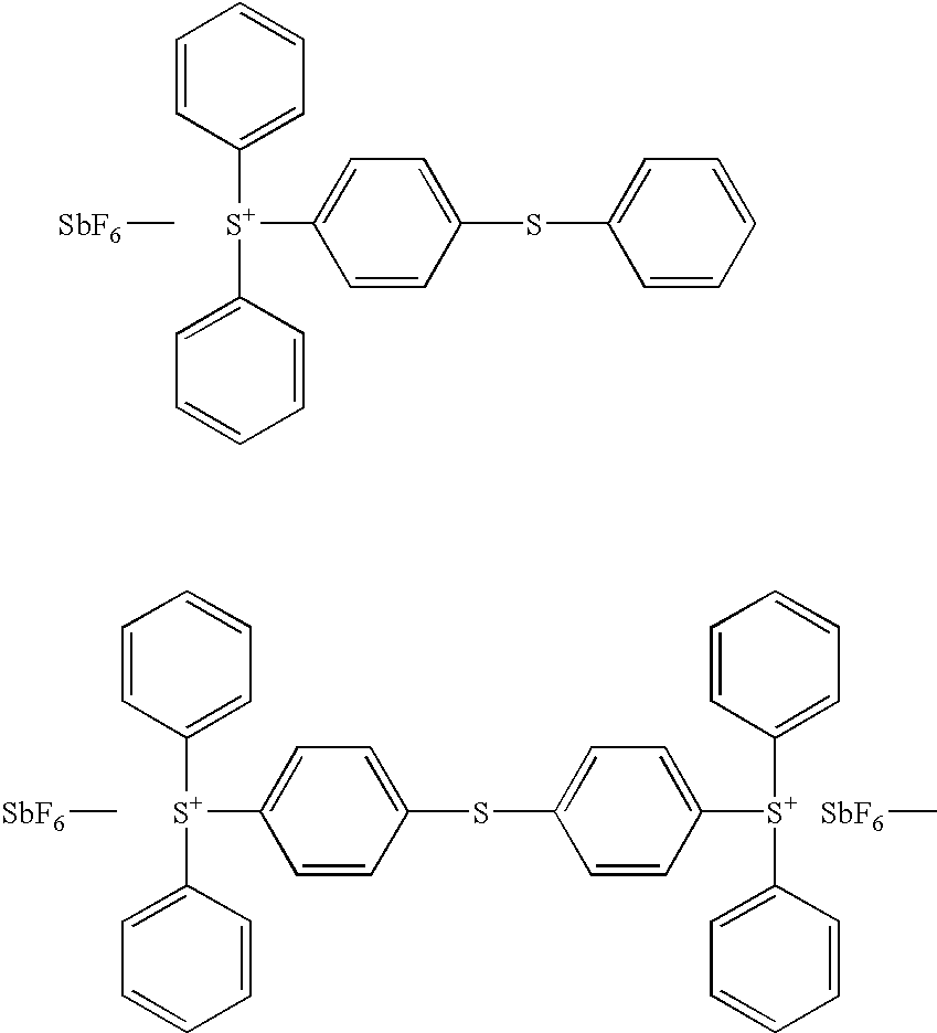


In some alternative embodiments, the chain extended diurethane methacrylate has the following structure:


In some alternative embodiments, the diisocyanate functionalized perfluoropolyether has the following structure:


-
- (i) a perfluoropolyether (PFPE) material having a characteristic selected from the group consisting of: a viscosity greater than about 100 centistokes (cSt) and a viscosity less than about 100 cSt, provided that the liquid PFPE precursor material having a viscosity less than 100 cSt is not a free-radically photocurable PFPE material;
- (ii) a functionalized PFPE material;
- (iii) a fluoroolefin-based elastomer; and
- (iv) combinations thereof;
-
- (i) a perfluoropolyether (PFPE) material having a characteristic selected from the group consisting of: a viscosity greater than about 100 centistokes (cSt) and a viscosity less than about 100 cSt, provided that the liquid PFPE precursor material having a viscosity less than 100 cSt is not a free-radically photocurable PFPE material;
- (ii) a functionalized PFPE material;
- (iii) a fluoroolefin-based elastomer; and
- (iv) combinations thereof; and wherein the microfluidics device includes one or more microscale channels, and wherein at least one of the one or more microscale channels includes an outlet aperture;
-
- (i) a perfluoropolyether (PFPE) material having a characteristic selected from the group consisting of: a viscosity greater than about 100 centistokes (cSt) and a viscosity less than about 100 cSt, provided that the liquid PFPE precursor material having a viscosity less than 100 cSt is not a free-radically photocurable PFPE material;
- (ii) a functionalized PFPE material;
- (iii) a fluoroolefin-based elastomer; and
- (iv) combinations thereof; and wherein the microfluidics device includes one or more microscale channels, and wherein at least one of the one or more microscale channels includes a separation region;


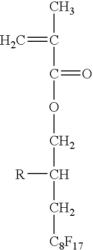


Claims (18)


Priority Applications (1)
| Application Number | Priority Date | Filing Date | Title |
|---|---|---|---|
| US12/063,284 US8158728B2 (en) | 2004-02-13 | 2006-08-09 | Methods and materials for fabricating microfluidic devices |
Applications Claiming Priority (7)
| Application Number | Priority Date | Filing Date | Title |
|---|---|---|---|
| US54490504P | 2004-02-13 | 2004-02-13 | |
| PCT/US2005/004421 WO2005084191A2 (en) | 2004-02-13 | 2005-02-14 | Functional materials and novel methods for the fabrication of microfluidic devices |
| US70678605P | 2005-08-09 | 2005-08-09 | |
| US73272705P | 2005-11-02 | 2005-11-02 | |
| US79931706P | 2006-05-10 | 2006-05-10 | |
| PCT/US2006/031067 WO2007021762A2 (en) | 2005-08-09 | 2006-08-09 | Methods and materials for fabricating microfluidic devices |
| US12/063,284 US8158728B2 (en) | 2004-02-13 | 2006-08-09 | Methods and materials for fabricating microfluidic devices |
Related Parent Applications (2)
| Application Number | Title | Priority Date | Filing Date |
|---|---|---|---|
| PCT/US2005/004421 Continuation-In-Part WO2005084191A2 (en) | 2004-02-13 | 2005-02-14 | Functional materials and novel methods for the fabrication of microfluidic devices |
| PCT/US2006/031067 A-371-Of-International WO2007021762A2 (en) | 2004-02-13 | 2006-08-09 | Methods and materials for fabricating microfluidic devices |
Related Child Applications (1)
| Application Number | Title | Priority Date | Filing Date |
|---|---|---|---|
| US13/438,431 Division US8444899B2 (en) | 2004-02-13 | 2012-04-03 | Methods and materials for fabricating microfluidic devices |
Publications (2)
| Publication Number | Publication Date |
|---|---|
| US20090281250A1 US20090281250A1 (en) | 2009-11-12 |
| US8158728B2 true US8158728B2 (en) | 2012-04-17 |
Family
ID=37758124
Family Applications (3)
| Application Number | Title | Priority Date | Filing Date |
|---|---|---|---|
| US12/063,284 Active 2025-11-29 US8158728B2 (en) | 2004-02-13 | 2006-08-09 | Methods and materials for fabricating microfluidic devices |
| US13/438,431 Active US8444899B2 (en) | 2004-02-13 | 2012-04-03 | Methods and materials for fabricating microfluidic devices |
| US13/859,323 Abandoned US20130228950A1 (en) | 2005-08-09 | 2013-04-09 | Methods and materials for fabricating microfluidic devices |
Family Applications After (2)
| Application Number | Title | Priority Date | Filing Date |
|---|---|---|---|
| US13/438,431 Active US8444899B2 (en) | 2004-02-13 | 2012-04-03 | Methods and materials for fabricating microfluidic devices |
| US13/859,323 Abandoned US20130228950A1 (en) | 2005-08-09 | 2013-04-09 | Methods and materials for fabricating microfluidic devices |
Country Status (3)
| Country | Link |
|---|---|
| US (3) | US8158728B2 (en) |
| EP (2) | EP1922364A4 (en) |
| WO (1) | WO2007021762A2 (en) |
Cited By (67)
| Publication number | Priority date | Publication date | Assignee | Title |
|---|---|---|---|---|
| US20110123711A1 (en) * | 2008-04-18 | 2011-05-26 | University Of Massachusetts Lowel | Methods for forming metal-polymer hybrid tooling for forming parts having micro features |
| US20110238151A1 (en) * | 2010-03-23 | 2011-09-29 | Boston Scientific Scimed, Inc. | Surface treated bioerodible metal endoprostheses |
| US20130066438A1 (en) * | 2011-07-06 | 2013-03-14 | Alexander M. Seifalian | Synthetic scaffolds and organ and tissue transplantation |
| US8506863B1 (en) * | 2008-10-02 | 2013-08-13 | California Institute Of Technology | Method for adhering a microfluidic chip to a substrate |
| US8715339B2 (en) | 2006-12-28 | 2014-05-06 | Boston Scientific Scimed, Inc. | Bioerodible endoprostheses and methods of making the same |
| US8808726B2 (en) | 2006-09-15 | 2014-08-19 | Boston Scientific Scimed. Inc. | Bioerodible endoprostheses and methods of making the same |
| WO2014126837A2 (en) | 2013-02-12 | 2014-08-21 | Eipi Systems, Inc. | Continuous liquid interphase printing |
| WO2014126830A2 (en) | 2013-02-12 | 2014-08-21 | Eipi Systems, Inc. | Method and apparatus for three-dimensional fabrication |
| US8840660B2 (en) | 2006-01-05 | 2014-09-23 | Boston Scientific Scimed, Inc. | Bioerodible endoprostheses and methods of making the same |
| WO2014204547A2 (en) | 2013-04-01 | 2014-12-24 | The University Of North Carolina At Chapel Hill | Ion conducting fluoropolymer carbonates for alkali metal ion batteries |
| WO2015142546A1 (en) | 2014-03-21 | 2015-09-24 | Carbon3D, Inc. | Method and apparatus for three-dimensional fabrication with gas injection through carrier |
| WO2015195920A1 (en) | 2014-06-20 | 2015-12-23 | Carbon3D, Inc. | Three-dimensional printing method using increased light intensity and apparatus therefore |
| WO2015195924A1 (en) | 2014-06-20 | 2015-12-23 | Carbon3D, Inc. | Three-dimensional printing with reciprocal feeding of polymerizable liquid |
| WO2015195909A1 (en) | 2014-06-20 | 2015-12-23 | Carbon3D, Inc. | Three-dimensional printing using tiled light engines |
| WO2015200201A1 (en) | 2014-06-23 | 2015-12-30 | Carbon3D, Inc. | Polyurethane resins having multiple mechanisms of hardening for use in producing three-dimensional objects |
| WO2016025579A1 (en) | 2014-08-12 | 2016-02-18 | Carbon3D, Inc. | Three-dimensional printing with build plates having a smooth or patterned surface and related methods |
| US9353313B2 (en) | 2012-08-09 | 2016-05-31 | Auburn University | Microdevices and methods of manufacture |
| WO2016109550A1 (en) | 2014-12-31 | 2016-07-07 | Carbon3D, Inc. | Three-dimensional printing of objects with breathing orifices |
| WO2016112084A1 (en) | 2015-01-06 | 2016-07-14 | Carbon3D, Inc. | Build plate for three dimensional printing having a rough or patterned surface |
| WO2016112090A1 (en) | 2015-01-07 | 2016-07-14 | Carbon3D, Inc. | Microfluidic devices and methods of making the same |
| WO2016115236A1 (en) | 2015-01-13 | 2016-07-21 | Carbon3D, Inc. | Three-dimensional printing with build plates having surface topologies for increasing permeability and related methods |
| WO2016123499A1 (en) | 2015-01-30 | 2016-08-04 | Carbon3D, Inc. | Build plates for continuous liquid interface printing having permeable base and adhesive for increasing permeability and related methods, systems and devices |
| WO2016123506A1 (en) | 2015-01-30 | 2016-08-04 | Carbon3D, Inc. | Build plates for continuous liquid interface printing having permeable sheets and related methods, systems and devices |
| WO2016126779A1 (en) | 2015-02-05 | 2016-08-11 | Carbon3D, Inc. | Method of additive manufacturing by fabrication through multiple zones |
| WO2016140891A1 (en) | 2015-03-05 | 2016-09-09 | Carbon3D, Inc. | Continuous liquid interface production with sequential patterned exposure |
| WO2016140886A1 (en) | 2015-03-05 | 2016-09-09 | Carbon3D, Inc. | Fabrication of three dimensional objects with multiple operating modes |
| WO2016140888A1 (en) | 2015-03-05 | 2016-09-09 | Carbon3D, Inc. | Fabrication of three dimensional objects with variable slice thickness |
| WO2016145050A1 (en) | 2015-03-10 | 2016-09-15 | Carbon3D, Inc. | Microfluidic devices having flexible features and methods of making the same |
| WO2016149151A1 (en) | 2015-03-13 | 2016-09-22 | Carbon3D, Inc. | Three-dimensional printing with concurrent delivery of different polymerizable liquids |
| WO2016149104A1 (en) | 2015-03-13 | 2016-09-22 | Carbon3D, Inc. | Three-dimensional printing with flexible build plates |
| WO2016149097A1 (en) | 2015-03-13 | 2016-09-22 | Carbon3D, Inc. | Three-dimensional printing with reduced pressure build plate unit |
| US20160301107A1 (en) * | 2015-04-07 | 2016-10-13 | Blue Current, Inc. | Functionalized perfluoroalkanes and electrolyte compositions |
| WO2016196365A1 (en) | 2015-05-29 | 2016-12-08 | Envisia Therapeutics, Inc. | Implant for treatment of an ocular condition |
| US9540312B2 (en) | 2015-02-03 | 2017-01-10 | Blue Current, Inc. | Non-flammable electrolyte composition including carbonate-terminated perfluoropolymer and phosphate-terminated or phosphonate-terminated perfluoropolymer and battery using same |
| US9541480B2 (en) | 2011-06-29 | 2017-01-10 | Academia Sinica | Capture, purification, and release of biological substances using a surface coating |
| WO2017015675A1 (en) | 2015-07-23 | 2017-01-26 | Envisia Therapeutics, Inc. | Glaucoma treatment via intracameral ocular implants |
| WO2017029602A2 (en) | 2015-08-16 | 2017-02-23 | Glaxosmithkline Intellectual Property Development Limited | Compounds for use in antibacterial applications |
| WO2017035408A1 (en) | 2015-08-26 | 2017-03-02 | Achillion Pharmaceuticals, Inc. | Compounds for treatment of immune and inflammatory disorders |
| WO2017053783A1 (en) | 2015-09-25 | 2017-03-30 | Carbon3D, Inc. | Build plate assemblies for continuous liquid interphase printing having lighting panels and related methods, systems and devices |
| WO2017085692A1 (en) | 2015-11-18 | 2017-05-26 | Glaxosmithkline Intellectual Property (No.2) Limited | Pharmaceutical compositions of ribavirin |
| WO2017112682A1 (en) | 2015-12-22 | 2017-06-29 | Carbon, Inc. | Fabrication of compound products from multiple intermediates by additive manufacturing with dual cure resins |
| WO2017112653A1 (en) | 2015-12-22 | 2017-06-29 | Carbon, Inc. | Dual precursor resin systems for additive manufacturing with dual cure resins |
| WO2017112571A1 (en) | 2015-12-22 | 2017-06-29 | Carbon, Inc. | Dual cure additive manufacturing of rigid intermediates that generate semi-rigid, flexible, or elastic final products |
| WO2017112521A1 (en) | 2015-12-22 | 2017-06-29 | Carbon, Inc. | Production of flexible products by additive manufacturing with dual cure resins |
| WO2017112483A2 (en) | 2015-12-22 | 2017-06-29 | Carbon, Inc. | Accelerants for additive manufacturing with dual cure resins |
| US9748604B2 (en) | 2012-10-19 | 2017-08-29 | The University Of North Carolina At Chapel Hill | Ion conducting polymers and polymer blends for alkali metal ion batteries |
| WO2017153316A1 (en) | 2016-03-07 | 2017-09-14 | Glaxosmithkline Biologicals Sa | Drug delivery particles |
| KR101793864B1 (en) | 2017-03-08 | 2017-11-06 | 인하대학교 산학협력단 | Superhydrophobic surface treatment based on anthracene-perfluoropolyether and method for treating the surface of superhydrophobic of PET fiber using the same |
| WO2018006018A1 (en) | 2016-07-01 | 2018-01-04 | Carbon, Inc. | Three-dimensional printing method and apparatus for reducing bubbles by de-gassing through build plate |
| WO2018005552A1 (en) | 2016-06-27 | 2018-01-04 | Achillion Pharmaceuticals, Inc. | Quinazoline and indole compounds to treat medical disorders |
| WO2018094227A1 (en) | 2016-11-17 | 2018-05-24 | The University Of North Carolina At Chapel Hill | Alkyl pyrrolopyrimidine analogs and methods of making and using same |
| US10107726B2 (en) | 2016-03-16 | 2018-10-23 | Cellmax, Ltd. | Collection of suspended cells using a transferable membrane |
| US10112198B2 (en) | 2014-08-26 | 2018-10-30 | Academia Sinica | Collector architecture layout design |
| US10384439B2 (en) | 2015-11-06 | 2019-08-20 | Stratasys, Inc. | Continuous liquid interface production system with viscosity pump |
| US10495644B2 (en) | 2014-04-01 | 2019-12-03 | Academia Sinica | Methods and systems for cancer diagnosis and prognosis |
| WO2020041301A1 (en) | 2018-08-20 | 2020-02-27 | Achillion Pharmaceuticals, Inc. | Pharmaceutical compounds for the treatment of complement factor d medical disorders |
| WO2020081723A1 (en) | 2018-10-16 | 2020-04-23 | Georgia State University Research Foundation, Inc. | Carbon monoxide prodrugs for the treatment of medical disorders |
| US10898494B2 (en) | 2016-05-05 | 2021-01-26 | Liquidia Technologies, Inc. | Dry powder treprostinil for the treatment of pulmonary hypertension |
| EP3861982A2 (en) | 2013-12-06 | 2021-08-11 | Allergan, Inc. | Intracameral implant for treatment of an ocular condition |
| US20210300100A1 (en) * | 2020-03-31 | 2021-09-30 | Canon Production Printing Holding B.V. | Method for applying an image onto the recording medium and corresponding printing apparatus |
| US11226278B2 (en) | 2016-11-08 | 2022-01-18 | Kennesaw State University Research And Service Foundation, Inc. | Leukocyte quantitation microfluidic method and device |
| US11268607B1 (en) | 2016-02-17 | 2022-03-08 | Helix Linear Technologies | Lead screw nuts having threads formed from different materials |
| EP4053117A1 (en) | 2015-08-26 | 2022-09-07 | Achillion Pharmaceuticals, Inc. | Aryl, heteroaryl, and heterocyclic compounds for treatment of medical disorders |
| US11708720B2 (en) | 2013-10-22 | 2023-07-25 | E Ink Corporation | Light-modulating electrophoretic device |
| US11733557B2 (en) | 2013-03-22 | 2023-08-22 | E Ink Corporation | Electrophoretic device having a transparent light state |
| US11867320B2 (en) | 2018-03-02 | 2024-01-09 | National Research Council Of Canada | Polymeric microfluidic valve |
| USD1016599S1 (en) | 2017-02-17 | 2024-03-05 | Helix Linear Technologies | Nut |
Families Citing this family (131)
| Publication number | Priority date | Publication date | Assignee | Title |
|---|---|---|---|---|
| US11243494B2 (en) | 2002-07-31 | 2022-02-08 | Abs Global, Inc. | Multiple laminar flow-based particle and cellular separation with laser steering |
| US9040090B2 (en) | 2003-12-19 | 2015-05-26 | The University Of North Carolina At Chapel Hill | Isolated and fixed micro and nano structures and methods thereof |
| US20070266801A1 (en) * | 2005-12-16 | 2007-11-22 | Alireza Khademhosseini | Reversible Sealing of Microfluidic Arrays |
| US8944804B2 (en) | 2006-01-04 | 2015-02-03 | Liquidia Technologies, Inc. | Nanostructured surfaces for biomedical/biomaterial applications and processes thereof |
| GB2443322B (en) * | 2006-10-28 | 2010-09-08 | P2I Ltd | Plasma coated microfabricated device or component thereof |
| GB0621520D0 (en) | 2006-10-28 | 2006-12-06 | P2I Ltd | Novel products |
| US8128393B2 (en) * | 2006-12-04 | 2012-03-06 | Liquidia Technologies, Inc. | Methods and materials for fabricating laminate nanomolds and nanoparticles therefrom |
| US20110168631A1 (en) * | 2006-12-15 | 2011-07-14 | General Electric Company | Methods and apparatuses for water filtration using polyarylether membranes |
| JP5604301B2 (en) | 2007-10-12 | 2014-10-08 | リクイディア・テクノロジーズ・インコーポレーテッド | Systems and methods for producing particles and patterned films |
| US20090191409A1 (en) * | 2008-01-25 | 2009-07-30 | Steve Simon | Combined Wetting/Non-Wetting Element For Low and High Surface Tension Liquids |
| US9893337B2 (en) | 2008-02-13 | 2018-02-13 | Seeo, Inc. | Multi-phase electrolyte lithium batteries |
| US9480461B2 (en) * | 2008-03-10 | 2016-11-01 | Volatile Analysis Corporation | Methods for extracting chemicals from nasal cavities and breath |
| US8034396B2 (en) | 2008-04-01 | 2011-10-11 | Tyco Healthcare Group Lp | Bioadhesive composition formed using click chemistry |
| KR100919400B1 (en) * | 2008-04-07 | 2009-09-29 | 삼성전자주식회사 | Microfluidic device and method for fabricating the same |
| WO2009158336A1 (en) * | 2008-06-25 | 2009-12-30 | Boston Scientific Scimed, Inc. | Medical devices having superhydrophobic surfaces |
| US20100098847A1 (en) * | 2008-10-21 | 2010-04-22 | Molecular Imprints, Inc. | Drop Deposition Materials for Imprint Lithography |
| JP5340760B2 (en) * | 2009-02-12 | 2013-11-13 | 倉敷紡績株式会社 | Fluid control method and fluid control apparatus |
| WO2010095052A2 (en) | 2009-02-21 | 2010-08-26 | Sofradim Production | Compounds and medical devices activated with solvophobic linkers |
| EP2398943B1 (en) | 2009-02-21 | 2013-04-17 | Sofradim Production | Crosslinked fibers and method of making same using uv radiation |
| US8512728B2 (en) | 2009-02-21 | 2013-08-20 | Sofradim Production | Method of forming a medical device on biological tissue |
| AU2010215931A1 (en) | 2009-02-21 | 2011-10-13 | Covidien Lp | Medical devices having activated surfaces |
| US8663689B2 (en) | 2009-02-21 | 2014-03-04 | Sofradim Production | Functionalized adhesive medical gel |
| AU2010215192B2 (en) | 2009-02-21 | 2015-04-30 | Sofradim Production | Amphiphilic compounds and self-assembling compositions made therefrom |
| EP2398584A2 (en) | 2009-02-21 | 2011-12-28 | Sofradim Production | Apparatus and method of reaching polymers by exposure to uv radiation to produce injectable medical devices |
| AU2010215936B2 (en) | 2009-02-21 | 2015-03-05 | Covidien Lp | Medical devices having activated surfaces |
| US8968733B2 (en) | 2009-02-21 | 2015-03-03 | Sofradim Production | Functionalized surgical adhesives |
| CA2753179A1 (en) | 2009-02-21 | 2010-08-26 | Sofradim Production | Crosslinked fibers and method of making same by extrusion |
| WO2010095047A2 (en) | 2009-02-21 | 2010-08-26 | Sofradim Production | Apparatus and method of reacting polymers passing through metal ion chelated resin matrix to produce injectable medical devices |
| CA2753173C (en) | 2009-02-21 | 2017-05-30 | Sofradim Production | Medical devices with an activated coating |
| US8535477B2 (en) | 2009-02-21 | 2013-09-17 | Sofradim Production | Medical devices incorporating functional adhesives |
| US8877170B2 (en) | 2009-02-21 | 2014-11-04 | Sofradim Production | Medical device with inflammatory response-reducing coating |
| EP2427801B1 (en) * | 2009-05-08 | 2017-08-09 | Hewlett-Packard Development Company, L.P. | Functionalized perfluoropolyether material as a hydrophobic coating |
| NL2005263A (en) * | 2009-09-29 | 2011-03-30 | Asml Netherlands Bv | Imprint lithography. |
| US8283569B2 (en) | 2010-01-22 | 2012-10-09 | The Regents Of The University Of Michigan | Electrode array and method of fabrication |
| AU2011231245B2 (en) | 2010-03-25 | 2015-03-26 | Covidien Lp | Medical devices incorporating functional adhesives |
| WO2011117745A2 (en) | 2010-03-25 | 2011-09-29 | Sofradim Production | Surgical fasteners and methods for sealing wounds |
| AU2011276443A1 (en) | 2010-06-29 | 2013-01-31 | Covidien Lp | Microwave-powered reactor and method for in situ forming implants |
| CA2804251A1 (en) | 2010-07-01 | 2012-01-05 | Sofradim Production | Medical device with predefined activated cellular integration |
| US9168679B2 (en) * | 2010-07-16 | 2015-10-27 | Northwestern University | Programmable soft lithography: solvent-assisted nanoscale embossing |
| EP2598178B1 (en) | 2010-07-27 | 2018-07-11 | Sofradim Production | Polymeric fibers having tissue reactive members |
| US10908066B2 (en) | 2010-11-16 | 2021-02-02 | 1087 Systems, Inc. | Use of vibrational spectroscopy for microfluidic liquid measurement |
| WO2012074994A1 (en) * | 2010-11-29 | 2012-06-07 | The Regents Of The University Of Colorado, A Body Corporate | Novel thermoreversible network scaffolds and methods of preparing same |
| JP5616309B2 (en) * | 2010-12-01 | 2014-10-29 | アークレイ株式会社 | Device and manufacturing method thereof |
| DE102011009923A1 (en) * | 2011-01-31 | 2012-08-02 | Mann + Hummel Gmbh | Ion exchanger for the treatment of a liquid fluid |
| DE102011102266B4 (en) * | 2011-05-23 | 2013-04-11 | Epcos Ag | Arrangement with a MEMS component with a PFPE layer and method for the production |
| ITMI20110995A1 (en) * | 2011-05-31 | 2012-12-01 | Ione | METHOD FOR THE PRODUCTION OF MONOLITHIC THREE-DIMENSIONAL MICROFLUID DEVICES |
| JP6082237B2 (en) * | 2011-12-09 | 2017-02-15 | 株式会社トクヤマ | Manufacturing method of silicon substrate having texture structure |
| EP2626133A1 (en) * | 2012-02-10 | 2013-08-14 | Chemtrix B.V. | Micro-fluidic system |
| US9802349B2 (en) | 2012-03-02 | 2017-10-31 | Taiwan Semiconductor Manufacturing Company, Ltd. | Wafer level transfer molding and apparatus for performing the same |
| US8951037B2 (en) | 2012-03-02 | 2015-02-10 | Taiwan Semiconductor Manufacturing Company, Ltd. | Wafer-level underfill and over-molding |
| WO2013159116A1 (en) | 2012-04-20 | 2013-10-24 | University Of Chicago | Fluidic devices for biospecimen preservation |
| CA2870999A1 (en) * | 2012-04-20 | 2013-10-24 | SlipChip, LLC | Fluidic devices and systems for sample preparation or autonomous analysis |
| JP5827180B2 (en) * | 2012-06-18 | 2015-12-02 | 富士フイルム株式会社 | Imprint curable composition and substrate adhesion composition, and semiconductor device using the same |
| EP2864764B1 (en) | 2012-06-20 | 2018-03-07 | The University of North Carolina At Chapel Hill | Integrated sample processing for electrospray ionization devices |
| MX343189B (en) * | 2012-06-29 | 2016-10-26 | Johnson & Johnson Vision Care | Multiple state electroactive ophthalmic device. |
| EP2871482B1 (en) * | 2012-07-09 | 2018-07-18 | Sony Corporation | Microchip and method for producing microchip |
| JP6077792B2 (en) * | 2012-08-28 | 2017-02-08 | 株式会社ブリヂストン | A member having at least a cured layer formed by curing a curable resin composition |
| US9623605B2 (en) * | 2012-09-12 | 2017-04-18 | International Business Machines Corporation | Thermally cross-linkable photo-hydrolyzable inkjet printable polymers for microfluidic channels |
| DE102012217487A1 (en) * | 2012-09-26 | 2014-04-17 | Agilent Technologies, Inc. - A Delaware Corporation - | Fluid interface between fluid lines of different cross sections |
| US9376311B2 (en) * | 2012-12-17 | 2016-06-28 | University Of Maryland, College Park | Method for fabricating thermoplastic fluidic devices by orogenic growth and fluidic devices manufactured thereby |
| CN104884487B (en) | 2012-12-28 | 2018-01-05 | 东洋合成工业株式会社 | Resin combination, resin die, optical pressure impression method and the manufacture method of integrated circuit and optical element |
| US20150352777A1 (en) * | 2013-01-18 | 2015-12-10 | The University Of North Carolina At Chapel Hill | High-throughput manufacturing of microneedles |
| US9308616B2 (en) | 2013-01-21 | 2016-04-12 | Innovative Finishes LLC | Refurbished component, electronic device including the same, and method of refurbishing a component of an electronic device |
| WO2014136731A1 (en) | 2013-03-04 | 2014-09-12 | 東洋合成工業株式会社 | Composition, resin mold, optical imprinting method, method for manufacturing optical element, and method for manufacturing electronic element |
| US9718056B2 (en) | 2013-03-15 | 2017-08-01 | Syracuse University | Microfluidics polymerase chain reaction and high resolution melt detection |
| WO2014179120A1 (en) * | 2013-05-01 | 2014-11-06 | Innovative Finishes LLC | Method of refurbishing an electronic device component |
| US9775928B2 (en) | 2013-06-18 | 2017-10-03 | Covidien Lp | Adhesive barbed filament |
| GB201311679D0 (en) | 2013-06-28 | 2013-08-14 | Ibm | Microfluidic chip with dielectrophoretic electrodes extending in hydrophilic flow path |
| US8961904B2 (en) | 2013-07-16 | 2015-02-24 | Premium Genetics (Uk) Ltd. | Microfluidic chip |
| DE102013012731A1 (en) * | 2013-08-01 | 2015-02-05 | Krohne Messtechnik Gmbh | Process for the preparation of a gas converter and corresponding gas converter |
| US10005248B2 (en) | 2013-09-20 | 2018-06-26 | The Regents Of The University Of California | Method and kit for forming plastic lenses from molds formed on surface with varied wettability |
| DE102013017317A1 (en) * | 2013-10-18 | 2015-04-23 | Endress + Hauser Flowtec Ag | Measuring arrangement with a carrier element and a sensor |
| US9045582B2 (en) * | 2013-10-29 | 2015-06-02 | Uop Llc | Cross-linked rubbery polyurethane-ether membranes for separations |
| US11796449B2 (en) | 2013-10-30 | 2023-10-24 | Abs Global, Inc. | Microfluidic system and method with focused energy apparatus |
| MY173073A (en) * | 2013-11-07 | 2019-12-24 | Agc Inc | Mold release film and process for producing semiconductor package |
| TW201520019A (en) * | 2013-11-20 | 2015-06-01 | Univ Nat Taiwan Science Tech | Fabrication method for three dimensional micro-structure of polymers |
| US9969964B2 (en) * | 2013-12-23 | 2018-05-15 | Purdue Research Foundation | Disease-on-a-chip |
| US10137673B2 (en) | 2013-12-31 | 2018-11-27 | Canon U.S. Life Sciences, Inc. | Methods and systems for continuous flow cell lysis in a microfluidic device |
| EP3145689B1 (en) | 2014-05-20 | 2020-01-01 | The Regents of the University of California | Layerless bioprinting via dynamic optical projection and uses thereof |
| US10620200B2 (en) * | 2014-05-29 | 2020-04-14 | The Board Of Regents Of The University Of Texas System | Methods and compositions for hybrid microfluidic devices integrated with nano-biosensors |
| WO2016033434A1 (en) * | 2014-08-29 | 2016-03-03 | Bio-Rad Laboratories, Inc. | Epoxy mold making and micromilling for microfluidics |
| WO2016040850A1 (en) * | 2014-09-11 | 2016-03-17 | Oregon State University | Microfluidic device for removal of constituents from blood |
| US9575226B2 (en) * | 2014-09-22 | 2017-02-21 | The Chinese University Of Hong Kong | Positive microcontact printing |
| US20160124205A1 (en) * | 2014-10-27 | 2016-05-05 | Yale University | Simple, Fast and Plasma-Free Method of Fabricating PDMS Microstructures on Glass by Pop Slide Pattering |
| US9896592B2 (en) * | 2014-11-21 | 2018-02-20 | Vernay Laboratories, Inc. | Temporary elastomeric functional barrier membrane and method of manufacture |
| SG11201706777QA (en) | 2015-02-19 | 2017-09-28 | Premium Genetics (Uk) Ltd | Scanning infrared measurement system |
| AU2016233335B2 (en) * | 2015-03-17 | 2021-03-25 | President And Fellows Of Harvard College | Automated membrane fabrication system |
| US11052388B2 (en) | 2015-03-27 | 2021-07-06 | Wageningen Universiteit | Method of manufacturing a microfluidic device |
| US9923245B2 (en) | 2015-04-03 | 2018-03-20 | Seeo, Inc. | Fluorinated alkali ion electrolytes with urethane groups |
| WO2016161465A1 (en) * | 2015-04-03 | 2016-10-06 | Seeo, Inc. | Fluorinated alkali ion electrolytes with urethane groups |
| WO2016164505A1 (en) | 2015-04-07 | 2016-10-13 | Seeo, Inc. | Fluorinated alkali ion electrolytes with cyclic carbonate groups |
| EP3085661B1 (en) * | 2015-04-21 | 2017-12-27 | JSR Corporation | Method of producing microfluidic device |
| JP6533305B2 (en) | 2015-05-12 | 2019-06-19 | シーオ インコーポレーテッドSeeo, Inc. | Copolymer comprising PEO polymer and fluorinated polymer as electrolyte for lithium battery |
| WO2016200559A1 (en) | 2015-06-09 | 2016-12-15 | Seeo, Inc. | Peo-based graft copolymers with pendant fluorinated groups for use as electrolytes |
| WO2017142950A1 (en) * | 2016-02-17 | 2017-08-24 | President And Fellows Of Harvard College | Microfluidic device for shear flow testing and methods for using the same |
| US20190168221A1 (en) * | 2016-04-15 | 2019-06-06 | Vortex Biosciences, Inc. | Microfluidic Chips and Cartridges and Systems Utilizing Microfluidic Chips and Cartridges |
| KR20190005894A (en) | 2016-05-10 | 2019-01-16 | 시오 인코퍼레이티드 | A fluorinated electrolyte having a nitrile group |
| US20190185629A1 (en) * | 2016-08-05 | 2019-06-20 | Microoptx Inc. | Polymeric devices and methods of making |
| EP3509750A2 (en) * | 2016-09-12 | 2019-07-17 | Premium Genetics (UK) Ltd. | Method and system for hydrophobic coating of microfluidic chips |
| US10725373B1 (en) * | 2016-10-21 | 2020-07-28 | Iowa State University Research Foundation, Inc. | Nano-patterning methods including: (1) patterning of nanophotonic structures at optical fiber tip for refractive index sensing and (2) plasmonic crystal incorporating graphene oxide gas sensor for detection of volatile organic compounds |
| US10538659B2 (en) * | 2016-12-20 | 2020-01-21 | Bio-Rad Laboratories, Inc. | UV graft on microfluidic devices |
| JP6968833B2 (en) | 2017-01-26 | 2021-11-17 | 昭和電工株式会社 | Fluorine-containing ether compounds, lubricants for magnetic recording media and magnetic recording media |
| WO2018226956A1 (en) | 2017-06-08 | 2018-12-13 | Integra Biosciences Ag | Sample and reagent reservoir kits and liners with anti-vacuum feature |
| US10597289B1 (en) * | 2017-07-17 | 2020-03-24 | Adam Woolley | 3D printer, resin, and interconnect |
| US11618023B2 (en) * | 2017-12-06 | 2023-04-04 | Samplix Aps | Microfluidic device and a method for provision of emulsion droplets |
| CN112119151A (en) * | 2018-03-02 | 2020-12-22 | 量子细胞公司 | Method, composition and apparatus for isolation and expression analysis of regions of interest from tissue |
| US20210022651A1 (en) * | 2018-03-23 | 2021-01-28 | The Regents Of The University Of California | Three-dimensional microfluidic actuation and sensing wearable device for in-situ biofluid processing and analysis |
| CN110433876B (en) * | 2018-05-03 | 2022-05-17 | 香港科技大学 | Microfluidic device, manufacturing method thereof, mask and method for filtering suspended particles |
| EP3796998A1 (en) | 2018-05-23 | 2021-03-31 | ABS Global, Inc. | Systems and methods for particle focusing in microchannels |
| WO2020035805A2 (en) * | 2018-08-14 | 2020-02-20 | Texas Tech University System | Methods and systems for making tilted and curved structures with high aspect ratios |
| US11767483B2 (en) | 2018-09-12 | 2023-09-26 | Resonac Corporation | Fluorine-containing ether compound, lubricant for magnetic recording medium, and magnetic recording medium |
| US11820953B2 (en) | 2019-03-12 | 2023-11-21 | Resonac Corporation | Fluorine-containing ether compound, lubricant for magnetic recording medium and magnetic recording medium |
| DE102019107090A1 (en) * | 2019-03-20 | 2020-09-24 | Joanneum Research Forschungsgesellschaft Mbh | Microstructure with thermoplastic embossing lacquer layer and manufacturing process |
| BR112021020390A2 (en) | 2019-04-18 | 2022-01-18 | Abs Global Inc | Cryoprotectant delivery system, cryopreservation system for delivering a cryoprotectant to a biological specimen, method for delivering a cryoprotectant to a biological specimen, delivery system, and method for preparing a biological specimen for cryopreservation |
| CN110054756A (en) * | 2019-04-26 | 2019-07-26 | 同济大学 | The polyurethane resin and preparation method thereof of organic-silicon-modified fluorine-containing carbon branch |
| CN110183598B (en) * | 2019-06-28 | 2020-03-10 | 苏州大学 | Light polymerization method of block copolymer of main chain type semi-fluorine alternative copolymer |
| JPWO2021054202A1 (en) | 2019-09-18 | 2021-03-25 | ||
| GB201913529D0 (en) * | 2019-09-19 | 2019-11-06 | Tanriverdi Ugur | Method And Apparatus |
| US11905365B2 (en) | 2019-12-26 | 2024-02-20 | Resonac Corporation | Fluorine-containing ether compound, lubricant for magnetic recording medium, and magnetic recording medium |
| US11628439B2 (en) | 2020-01-13 | 2023-04-18 | Abs Global, Inc. | Single-sheath microfluidic chip |
| DE102020114621A1 (en) * | 2020-06-02 | 2021-12-02 | Joanneum Research Forschungsgesellschaft Mbh | Component with microfluidic structures, manufacturing process and use |
| US11833742B2 (en) | 2020-06-26 | 2023-12-05 | The Regents Of The University Of California | High-fidelity 3D printing using flashing photopolymerization |
| CN111701629B (en) * | 2020-07-03 | 2021-04-02 | 清华大学 | Super-hydrophobic micro-pit array chip and preparation method and device thereof |
| US11813608B2 (en) | 2020-09-22 | 2023-11-14 | Oregon State University | Fiber substrate-based fluidic analytical devices and methods of making and using the same |
| GB2603487A (en) * | 2021-02-04 | 2022-08-10 | Stewart Callum | Composition |
| CA3212659A1 (en) * | 2021-03-11 | 2022-09-15 | President And Fellows Of Harvard College | Fluorinated elastomers for brain probes and other applications |
| CN113527860B (en) * | 2021-06-29 | 2022-07-19 | 江西岳峰集团环保新材有限公司 | Preparation method of PPO composite material with high melt flowability |
| NL2030209B1 (en) | 2021-12-21 | 2023-06-29 | Surfix B V | Process for manufacturing a microfluidic device |
| CN114177962A (en) * | 2022-01-07 | 2022-03-15 | 中国科学院青岛生物能源与过程研究所 | Method for manufacturing sandwich micro-fluidic chip |
| DE102022107894A1 (en) * | 2022-04-01 | 2023-10-05 | Eberhard Karls Universität Tübingen, Körperschaft des öffentlichen Rechts | Method of manufacturing a reactor, reactors and assemblies |
| CN115433340B (en) * | 2022-09-26 | 2023-12-22 | 山东安然纳米实业发展有限公司 | Preparation method of photo-curing functional slurry, preparation method of functional fiber and functional fiber |
Citations (107)
| Publication number | Priority date | Publication date | Assignee | Title |
|---|---|---|---|---|
| US3810874A (en) | 1969-03-10 | 1974-05-14 | Minnesota Mining & Mfg | Polymers prepared from poly(perfluoro-alkylene oxide) compounds |
| US4352874A (en) | 1981-09-02 | 1982-10-05 | Polaroid Corporation | Method for forming a photosensitive silver halide element |
| US4353977A (en) | 1981-09-02 | 1982-10-12 | Polaroid Corporation | Method for forming a photosensitive silver halide element |
| US4356257A (en) | 1981-09-02 | 1982-10-26 | Polaroid Corporation | Photosensitive silver halide element and method of preparing same |
| US4359526A (en) | 1981-09-02 | 1982-11-16 | Polaroid Corporation | Method for forming a photosensitive silver halide element |
| US4512848A (en) | 1984-02-06 | 1985-04-23 | Exxon Research And Engineering Co. | Procedure for fabrication of microstructures over large areas using physical replication |
| US4614667A (en) | 1984-05-21 | 1986-09-30 | Minnesota Mining And Manufacturing Company | Composite low surface energy liner of perfluoropolyether |
| US4663274A (en) | 1985-04-01 | 1987-05-05 | Polaroid Corporation | Method for forming a photosensitive silver halide element |
| US4681925A (en) | 1985-02-22 | 1987-07-21 | Ausimont S.P.A. | Fluorinated polyacrylates and polyacrylamides having a controlled cross-linking degree, and process for preparing same |
| US4818801A (en) | 1982-01-18 | 1989-04-04 | Minnesota Mining And Manufacturing Company | Ophthalmic device comprising a polymer of a telechelic perfluoropolyether |
| US4830910A (en) | 1987-11-18 | 1989-05-16 | Minnesota Mining And Manufacturing Company | Low adhesion compositions of perfluoropolyethers |
| US5041359A (en) | 1985-04-03 | 1991-08-20 | Stork Screens B.V. | Method for forming a patterned photopolymer coating on a printing roller |
| US5175030A (en) | 1989-02-10 | 1992-12-29 | Minnesota Mining And Manufacturing Company | Microstructure-bearing composite plastic articles and method of making |
| US5189135A (en) | 1989-06-28 | 1993-02-23 | Syremont S.P.A. | Fluorinated polyurethanes with hydroxy functionality, process for preparing them and their use for the treatment of lithoidal material |
| US5259926A (en) | 1991-09-24 | 1993-11-09 | Hitachi, Ltd. | Method of manufacturing a thin-film pattern on a substrate |
| US5268405A (en) | 1993-03-31 | 1993-12-07 | E. I. Du Pont De Nemours And Company | Low temperature perfluoroelastomers |
| US5279689A (en) | 1989-06-30 | 1994-01-18 | E. I. Du Pont De Nemours And Company | Method for replicating holographic optical elements |
| US5368789A (en) | 1990-09-28 | 1994-11-29 | Canon Kabushiki Kaisha | Method for forming substrate sheet for optical recording medium |
| US5425848A (en) | 1993-03-16 | 1995-06-20 | U.S. Philips Corporation | Method of providing a patterned relief of cured photoresist on a flat substrate surface and device for carrying out such a method |
| US5512131A (en) | 1993-10-04 | 1996-04-30 | President And Fellows Of Harvard College | Formation of microstamped patterns on surfaces and derivative articles |
| US5630902A (en) | 1994-12-30 | 1997-05-20 | Honeywell Inc. | Apparatus for use in high fidelty replication of diffractive optical elements |
| US5753150A (en) | 1994-06-10 | 1998-05-19 | Johnson & Johnson Vision Products, Inc. | Low oxygen molding of soft contact lenses |
| US5772905A (en) | 1995-11-15 | 1998-06-30 | Regents Of The University Of Minnesota | Nanoimprint lithography |
| US5817242A (en) | 1995-08-04 | 1998-10-06 | International Business Machines Corporation | Stamp for a lithographic process |
| US5965631A (en) | 1994-09-06 | 1999-10-12 | Ciba Vision Corporation | Extended wear ophthalmic lens |
| US5994133A (en) | 1995-04-04 | 1999-11-30 | Novartis Ag | Cell growth substrate polymer |
| US6027595A (en) | 1998-07-02 | 2000-02-22 | Samsung Electronics Co., Ltd. | Method of making optical replicas by stamping in photoresist and replicas formed thereby |
| US6027630A (en) | 1997-04-04 | 2000-02-22 | University Of Southern California | Method for electrochemical fabrication |
| US6054537A (en) | 1992-12-10 | 2000-04-25 | Daikin Industries, Ltd. | Thermoplastic resin composition |
| US6083971A (en) | 1996-07-18 | 2000-07-04 | Hoffmann-La Roche Inc. | Certain oxopyrolo-pyrrole derivatives having thrombin inhibiting activity |
| US6204296B1 (en) | 1992-10-27 | 2001-03-20 | Alliance Pharmaceutical Corp. | Patient oxygenation using stabilized fluorocarbon emulsions |
| US6207758B1 (en) | 1997-12-15 | 2001-03-27 | Ausimont S.P.A. | Fluorinated thermoplastic elastomers |
| US6228318B1 (en) | 1999-03-24 | 2001-05-08 | Sumitomo Electric Industries, Ltd. | Manufacturing method of ceramics component having microstructure |
| US6247986B1 (en) | 1998-12-23 | 2001-06-19 | 3M Innovative Properties Company | Method for precise molding and alignment of structures on a substrate using a stretchable mold |
| US6284072B1 (en) | 1996-11-09 | 2001-09-04 | Epigem Limited | Multifunctional microstructures and preparation thereof |
| US6294450B1 (en) | 2000-03-01 | 2001-09-25 | Hewlett-Packard Company | Nanoscale patterning for the formation of extensive wires |
| US6300042B1 (en) | 1998-11-24 | 2001-10-09 | Motorola, Inc. | Lithographic printing method using a low surface energy layer |
| US6306563B1 (en) | 1999-06-21 | 2001-10-23 | Corning Inc. | Optical devices made from radiation curable fluorinated compositions |
| US6334960B1 (en) | 1999-03-11 | 2002-01-01 | Board Of Regents, The University Of Texas System | Step and flash imprint lithography |
| US6335224B1 (en) | 2000-05-16 | 2002-01-01 | Sandia Corporation | Protection of microelectronic devices during packaging |
| WO2002014078A2 (en) | 2000-08-14 | 2002-02-21 | Surface Logix, Inc. | Deformable stamp for patterning three-dimensional surfaces |
| US6355198B1 (en) | 1996-03-15 | 2002-03-12 | President And Fellows Of Harvard College | Method of forming articles including waveguides via capillary micromolding and microtransfer molding |
| US6375870B1 (en) | 1998-11-17 | 2002-04-23 | Corning Incorporated | Replicating a nanoscale pattern |
| US6422528B1 (en) | 2001-01-17 | 2002-07-23 | Sandia National Laboratories | Sacrificial plastic mold with electroplatable base |
| US20020156531A1 (en) | 1994-05-06 | 2002-10-24 | Felt Jeffrey C. | Biomaterial system for in situ tissue repair |
| US20030006527A1 (en) | 2001-06-22 | 2003-01-09 | Rabolt John F. | Method of fabricating micron-and submicron-scale elastomeric templates for surface patterning |
| WO2003005124A1 (en) | 2001-07-05 | 2003-01-16 | Obducat Aktiebolag | A stamp having an antisticking layer and a method of forming of repairing such a stamp |
| US6518189B1 (en) | 1995-11-15 | 2003-02-11 | Regents Of The University Of Minnesota | Method and apparatus for high density nanostructures |
| US6517995B1 (en) | 1999-09-14 | 2003-02-11 | Massachusetts Institute Of Technology | Fabrication of finely featured devices by liquid embossing |
| US20030062334A1 (en) | 2001-09-25 | 2003-04-03 | Lee Hong Hie | Method for forming a micro-pattern on a substrate by using capillary force |
| WO2003031096A2 (en) | 2001-10-11 | 2003-04-17 | Brewer Science, Inc. | Patterned structure reproduction using nonsticking mold |
| US6555221B1 (en) | 1998-10-26 | 2003-04-29 | The University Of Tokyo | Method for forming an ultra microparticle-structure |
| US20030139521A1 (en) | 2001-05-21 | 2003-07-24 | Linert Jeffrey G. | Polymers containing perfluorovinyl ethers and applications for such polymers |
| US6607683B1 (en) | 1998-09-04 | 2003-08-19 | Bruce E. Harrington | Methods and apparatus for producing manufactured articles having natural characteristics |
| WO2003072625A1 (en) | 2002-02-28 | 2003-09-04 | Luvantix Co., Ltd. | Photocurable resin composition for optical waveguide and optical waveguide made of the same |
| US6620196B1 (en) | 2000-08-30 | 2003-09-16 | Sdgi Holdings, Inc. | Intervertebral disc nucleus implants and methods |
| US20030205552A1 (en) | 1999-11-17 | 2003-11-06 | The Regents Of The University Of California | Method of forming a membrane with nanometer scale pores and application to biofiltration |
| US6645432B1 (en) | 2000-05-25 | 2003-11-11 | President & Fellows Of Harvard College | Microfluidic systems including three-dimensionally arrayed channel networks |
| US6649715B1 (en) | 2000-06-27 | 2003-11-18 | Clemson University | Fluoropolymers and methods of applying fluoropolymers in molding processes |
| US6653030B2 (en) | 2002-01-23 | 2003-11-25 | Hewlett-Packard Development Company, L.P. | Optical-mechanical feature fabrication during manufacture of semiconductors and other micro-devices and nano-devices that include micron and sub-micron features |
| US6656398B2 (en) | 2001-06-19 | 2003-12-02 | Corning Incorporated | Process of making a pattern in a film |
| US6656308B2 (en) | 2002-04-22 | 2003-12-02 | International Business Machines Corporation | Process of fabricating a precision microcontact printing stamp |
| US6663820B2 (en) | 2001-03-14 | 2003-12-16 | The Procter & Gamble Company | Method of manufacturing microneedle structures using soft lithography and photolithography |
| US6673397B2 (en) * | 2000-07-03 | 2004-01-06 | Adhesives Research, Inc. | Method of production of a crosslinked perfluorinated polyether release film |
| US6686184B1 (en) | 2000-05-25 | 2004-02-03 | President And Fellows Of Harvard College | Patterning of surfaces utilizing microfluidic stamps including three-dimensionally arrayed channel networks |
| US6689900B2 (en) | 2001-02-09 | 2004-02-10 | E. I. Du Pont De Nemours And Company | Fluorinated crosslinker and composition |
| US20040028804A1 (en) | 2002-08-07 | 2004-02-12 | Anderson Daniel G. | Production of polymeric microarrays |
| US6696220B2 (en) | 2000-10-12 | 2004-02-24 | Board Of Regents, The University Of Texas System | Template for room temperature, low pressure micro-and nano-imprint lithography |
| US6699347B2 (en) | 2002-05-20 | 2004-03-02 | The Procter & Gamble Company | High speed embossing and adhesive printing process |
| US20040046271A1 (en) | 2002-09-05 | 2004-03-11 | Watts Michael P.C. | Functional patterning material for imprint lithography processes |
| US20040053009A1 (en) | 2000-06-07 | 2004-03-18 | Ozin Geoffrey Alan | Method of self-assembly and optical applications of crystalline colloidal patterns on substrates |
| US20040065252A1 (en) | 2002-10-04 | 2004-04-08 | Sreenivasan Sidlgata V. | Method of forming a layer on a substrate to facilitate fabrication of metrology standards |
| US6719868B1 (en) | 1998-03-23 | 2004-04-13 | President And Fellows Of Harvard College | Methods for fabricating microfluidic structures |
| US20040110856A1 (en) | 2002-12-04 | 2004-06-10 | Young Jung Gun | Polymer solution for nanoimprint lithography to reduce imprint temperature and pressure |
| US6753131B1 (en) | 1996-07-22 | 2004-06-22 | President And Fellows Of Harvard College | Transparent elastomeric, contact-mode photolithography mask, sensor, and wavefront engineering element |
| US6755984B2 (en) | 2002-10-24 | 2004-06-29 | Hewlett-Packard Development Company, L.P. | Micro-casted silicon carbide nano-imprinting stamp |
| US20040123658A1 (en) | 2002-11-01 | 2004-07-01 | Kirby Brian J. | High dielectric strength microvalves |
| US6759182B2 (en) | 2001-03-06 | 2004-07-06 | Omron Corporation | Manufacturing method and apparatus of optical device and reflection plate provided with resin thin film having micro-asperity pattern |
| US20040137734A1 (en) | 1995-11-15 | 2004-07-15 | Princeton University | Compositions and processes for nanoimprinting |
| US6770721B1 (en) | 2000-11-02 | 2004-08-03 | Surface Logix, Inc. | Polymer gel contact masks and methods and molds for making same |
| US6783717B2 (en) | 2002-04-22 | 2004-08-31 | International Business Machines Corporation | Process of fabricating a precision microcontact printing stamp |
| US20040182711A1 (en) * | 2003-01-30 | 2004-09-23 | Rong-Chang Liang | High performance capsules for electrophoretic displays |
| US20040202865A1 (en) | 2003-04-08 | 2004-10-14 | Andrew Homola | Release coating for stamper |
| US6808646B1 (en) | 2003-04-29 | 2004-10-26 | Hewlett-Packard Development Company, L.P. | Method of replicating a high resolution three-dimensional imprint pattern on a compliant media of arbitrary size |
| US20040219246A1 (en) | 2003-04-29 | 2004-11-04 | Jeans Albert H. | Apparatus for embossing a flexible substrate with a pattern carried by an optically transparent compliant media |
| US6829050B2 (en) | 2001-01-22 | 2004-12-07 | Omron Corporation | Optical device provided with a resin thin film having a micro-asperity pattern and manufacturing method and apparatus of the optical device |
| US6849558B2 (en) | 2002-05-22 | 2005-02-01 | The Board Of Trustees Of The Leland Stanford Junior University | Replication and transfer of microstructures and nanostructures |
| US20050038180A1 (en) | 2003-08-13 | 2005-02-17 | Jeans Albert H. | Silicone elastomer material for high-resolution lithography |
| US6860956B2 (en) | 2003-05-23 | 2005-03-01 | Agency For Science, Technology & Research | Methods of creating patterns on substrates and articles of manufacture resulting therefrom |
| US6869557B1 (en) | 2002-03-29 | 2005-03-22 | Seagate Technology Llc | Multi-level stamper for improved thermal imprint lithography |
| US20050061773A1 (en) | 2003-08-21 | 2005-03-24 | Byung-Jin Choi | Capillary imprinting technique |
| US6900881B2 (en) | 2002-07-11 | 2005-05-31 | Molecular Imprints, Inc. | Step and repeat imprint lithography systems |
| US20050120902A1 (en) | 2001-04-25 | 2005-06-09 | David Adams | Edge transfer lithography |
| US20050142315A1 (en) * | 2003-12-24 | 2005-06-30 | Desimone Joseph M. | Liquid perfluoropolymers and medical applications incorporating same |
| EP1551066A1 (en) | 2002-09-19 | 2005-07-06 | Daikin Industries, Ltd. | Material with pattern surface for use as template and process for producing the same |
| US6923930B2 (en) | 2000-01-21 | 2005-08-02 | Obducat Aktiebolag | Mold for nano imprinting |
| US6929899B2 (en) | 2001-01-25 | 2005-08-16 | E. I. Du Pont De Nemours And Company | Fluorinated photopolymer composition and waveguide device |
| US6932934B2 (en) | 2002-07-11 | 2005-08-23 | Molecular Imprints, Inc. | Formation of discontinuous films during an imprint lithography process |
| US6936181B2 (en) | 2001-10-11 | 2005-08-30 | Kovio, Inc. | Methods for patterning using liquid embossing |
| US6953653B2 (en) | 2001-08-30 | 2005-10-11 | Clemson University | Fluoropolymer compositions, optical devices, and methods for fabricating optical devices |
| WO2005101466A2 (en) | 2003-12-19 | 2005-10-27 | The University Of North Carolina At Chapel Hill | Methods for fabricating isolated micro- and nano- structures using soft or imprint lithography |
| US6964793B2 (en) | 2002-05-16 | 2005-11-15 | Board Of Regents, The University Of Texas System | Method for fabricating nanoscale patterns in light curable compositions using an electric field |
| US6976424B2 (en) | 1999-12-31 | 2005-12-20 | International Business Machines Corporation | Stamp device for printing a pattern on a surface of a substrate |
| WO2006083311A2 (en) | 2005-02-03 | 2006-08-10 | Charles Tomasino | Scratch resistant gradient coating and coated articles |
| US7117790B2 (en) | 2002-01-11 | 2006-10-10 | Massachusetts Institute Of Technology | Microcontact printing |
| US7254278B2 (en) | 2002-01-16 | 2007-08-07 | Koninklijke Philips Electronics N.V. | Digital image processing method |
| US7294294B1 (en) | 2000-10-17 | 2007-11-13 | Seagate Technology Llc | Surface modified stamper for imprint lithography |
Family Cites Families (110)
| Publication number | Priority date | Publication date | Assignee | Title |
|---|---|---|---|---|
| BE755943A (en) | 1969-09-10 | 1971-03-09 | Rhone Poulenc Sa | PROCESS FOR PREPARING UNSATURATED ORGANOSILICIC COMPOUNDS |
| US3739015A (en) | 1970-09-04 | 1973-06-12 | Tanabe Seiyaku Co | Esters of p-phenoxy and p-alkoxy cinnamic acid |
| BE787487A (en) | 1971-08-13 | 1973-02-12 | Ciba Geigy | AGENTS FOR REGULATING PLANT GROWTH |
| US4694045A (en) | 1985-12-11 | 1987-09-15 | E. I. Du Pont De Nemours And Company | Base resistant fluoroelastomers |
| JPS6257448A (en) * | 1985-09-05 | 1987-03-13 | Mitsubishi Petrochem Co Ltd | Eluororesin composition |
| JPH0759669B2 (en) * | 1986-10-20 | 1995-06-28 | エヌティエヌ株式会社 | Lubricating resin composition |
| US5770029A (en) | 1996-07-30 | 1998-06-23 | Soane Biosciences | Integrated electrophoretic microdevices |
| JPH04288305A (en) | 1991-03-15 | 1992-10-13 | Nippon Mektron Ltd | Production of peroxide-vulcanizable fluoroelastomer |
| DE4114598A1 (en) | 1991-05-04 | 1992-11-05 | Bayer Ag | UNCROSSLINKED COPOLYMERISATES WITH REACTIVE DOUBLE BINDINGS FROM FLUOROMONERIC AND NON-CONJUGATED SERVES AND METHOD FOR THEIR PRODUCTION |
| DE4125201C1 (en) | 1991-07-30 | 1992-10-01 | Fraunhofer-Gesellschaft Zur Foerderung Der Angewandten Forschung Ev, 8000 Muenchen, De | |
| US5883632A (en) | 1992-05-04 | 1999-03-16 | Hewlett-Packard Company | Coordinating color produced by two devices--using a hue-controlled machine color space, or surface scaling |
| US5639423A (en) | 1992-08-31 | 1997-06-17 | The Regents Of The University Of Calfornia | Microfabricated reactor |
| US5958202A (en) | 1992-09-14 | 1999-09-28 | Perseptive Biosystems, Inc. | Capillary electrophoresis enzyme immunoassay |
| US5412034A (en) * | 1993-10-26 | 1995-05-02 | E. I. Du Pont De Nemours And Company | Curable elastomeric blends |
| IT1265461B1 (en) | 1993-12-29 | 1996-11-22 | Ausimont Spa | FLUOROELASTOMERS INCLUDING MONOMERIC UNITS ARISING FROM A BIS-OLEPHINE |
| IT1269514B (en) | 1994-05-18 | 1997-04-01 | Ausimont Spa | VULCANIZABLE FLUOROELASTOMERS PEROXIDE, PARTICULARLY SUITABLE FOR O-RING MANUFACTURE |
| US5459202A (en) * | 1994-06-30 | 1995-10-17 | E. I. Du Pont De Nemours And Company | Elastomer seal |
| JP3327016B2 (en) | 1994-12-06 | 2002-09-24 | ダイキン工業株式会社 | Fluororubber copolymer excellent in low-temperature sealability and its curing composition |
| DE69630737T2 (en) | 1995-07-17 | 2004-09-30 | Chisso Corp. | Silacyclopentadiene derivatives and organic electroluminescent elements containing them |
| US6130098A (en) | 1995-09-15 | 2000-10-10 | The Regents Of The University Of Michigan | Moving microdroplets |
| US6068751A (en) | 1995-12-18 | 2000-05-30 | Neukermans; Armand P. | Microfluidic valve and integrated microfluidic system |
| EP0868447B1 (en) | 1995-12-20 | 2000-02-23 | E.I. Du Pont De Nemours And Company | Iodonitriles as chain transfer agents in the manufacture of perfluoropolymers |
| CA2248045C (en) | 1996-04-04 | 2006-11-07 | Novartis Ag | High water content porous polymer |
| US5942443A (en) | 1996-06-28 | 1999-08-24 | Caliper Technologies Corporation | High throughput screening assay systems in microscale fluidic devices |
| US5939291A (en) | 1996-06-14 | 1999-08-17 | Sarnoff Corporation | Microfluidic method for nucleic acid amplification |
| NZ333346A (en) | 1996-06-28 | 2000-03-27 | Caliper Techn Corp | High-throughput screening assay systems in microscale fluidic devices |
| US6391622B1 (en) | 1997-04-04 | 2002-05-21 | Caliper Technologies Corp. | Closed-loop biochemical analyzers |
| US6091433A (en) | 1997-06-11 | 2000-07-18 | Eastman Kodak Company | Contact microfluidic printing apparatus |
| US6833242B2 (en) | 1997-09-23 | 2004-12-21 | California Institute Of Technology | Methods for detecting and sorting polynucleotides based on size |
| US5993611A (en) | 1997-09-24 | 1999-11-30 | Sarnoff Corporation | Capacitive denaturation of nucleic acid |
| US6012902A (en) | 1997-09-25 | 2000-01-11 | Caliper Technologies Corp. | Micropump |
| US6334676B1 (en) | 1997-09-29 | 2002-01-01 | Eastman Kodak Company | Using colorant precursors and reactants in microfluidic printing |
| US6451396B1 (en) | 1998-02-13 | 2002-09-17 | Gore Enterprise Holdings, Inc. | Flexure endurant composite elastomer compositions |
| US6100541A (en) | 1998-02-24 | 2000-08-08 | Caliper Technologies Corporation | Microfluidic devices and systems incorporating integrated optical elements |
| US6444474B1 (en) | 1998-04-22 | 2002-09-03 | Eltron Research, Inc. | Microfluidic system for measurement of total organic carbon |
| US6274089B1 (en) | 1998-06-08 | 2001-08-14 | Caliper Technologies Corp. | Microfluidic devices, systems and methods for performing integrated reactions and separations |
| US6529835B1 (en) | 1998-06-25 | 2003-03-04 | Caliper Technologies Corp. | High throughput methods, systems and apparatus for performing cell based screening assays |
| US6121404A (en) | 1998-07-06 | 2000-09-19 | Dow Corning Corporation | β-diketo functional organosilicon compounds |
| US6132685A (en) | 1998-08-10 | 2000-10-17 | Caliper Technologies Corporation | High throughput microfluidic systems and methods |
| US6447724B1 (en) | 1998-08-11 | 2002-09-10 | Caliper Technologies Corp. | DNA sequencing using multiple fluorescent labels being distinguishable by their decay times |
| US6482306B1 (en) | 1998-09-22 | 2002-11-19 | University Of Washington | Meso- and microfluidic continuous flow and stopped flow electroösmotic mixer |
| DE69907249T2 (en) | 1998-10-08 | 2004-01-29 | Astrazeneca Ab | MICROFABRICATED CELL INJECTOR |
| US6591852B1 (en) | 1998-10-13 | 2003-07-15 | Biomicro Systems, Inc. | Fluid circuit components based upon passive fluid dynamics |
| US6749814B1 (en) | 1999-03-03 | 2004-06-15 | Symyx Technologies, Inc. | Chemical processing microsystems comprising parallel flow microreactors and methods for using same |
| US6818112B2 (en) | 1999-04-20 | 2004-11-16 | Target Discovery, Inc. | Protein separation via multidimensional electrophoresis |
| US6592821B1 (en) | 1999-05-17 | 2003-07-15 | Caliper Technologies Corp. | Focusing of microparticles in microfluidic systems |
| US6406605B1 (en) | 1999-06-01 | 2002-06-18 | Ysi Incorporated | Electroosmotic flow controlled microfluidic devices |
| JP3370044B2 (en) | 1999-06-03 | 2003-01-27 | 東海化成工業株式会社 | Skin, manufacturing method thereof, manufacturing method of airbag door skin, and airbag door structure |
| CA2721172C (en) | 1999-06-28 | 2012-04-10 | California Institute Of Technology | Microfabricated elastomeric valve and pump systems |
| US7306672B2 (en) | 2001-04-06 | 2007-12-11 | California Institute Of Technology | Microfluidic free interface diffusion techniques |
| US6444106B1 (en) | 1999-07-09 | 2002-09-03 | Orchid Biosciences, Inc. | Method of moving fluid in a microfluidic device |
| US6613581B1 (en) | 1999-08-26 | 2003-09-02 | Caliper Technologies Corp. | Microfluidic analytic detection assays, devices, and integrated systems |
| DE19946916A1 (en) | 1999-09-30 | 2001-04-26 | Abb Research Ltd | Mold release agent for thermoset molded parts |
| WO2001026813A2 (en) | 1999-10-08 | 2001-04-19 | Micronics, Inc. | Microfluidics without electrically of mechanically operated pumps |
| US6875619B2 (en) | 1999-11-12 | 2005-04-05 | Motorola, Inc. | Microfluidic devices comprising biochannels |
| US6575562B1 (en) | 1999-11-16 | 2003-06-10 | Lexmark International, Inc. | Performance inkjet printhead chip layouts and assemblies |
| US6620625B2 (en) | 2000-01-06 | 2003-09-16 | Caliper Technologies Corp. | Ultra high throughput sampling and analysis systems and methods |
| US6358387B1 (en) | 2000-03-27 | 2002-03-19 | Caliper Technologies Corporation | Ultra high throughput microfluidic analytical systems and methods |
| AU5121801A (en) | 2000-03-31 | 2001-10-15 | Micronics Inc | Protein crystallization in microfluidic structures |
| US7351376B1 (en) | 2000-06-05 | 2008-04-01 | California Institute Of Technology | Integrated active flux microfluidic devices and methods |
| AU2001267930A1 (en) | 2000-06-22 | 2002-01-02 | Dsm N.V. | Radiation curable colored coating composition |
| US6508988B1 (en) | 2000-10-03 | 2003-01-21 | California Institute Of Technology | Combinatorial synthesis system |
| US6512063B2 (en) | 2000-10-04 | 2003-01-28 | Dupont Dow Elastomers L.L.C. | Process for producing fluoroelastomers |
| AU2001296551A1 (en) | 2000-10-05 | 2002-04-15 | E.I. Du Pont De Nemours And Company | Polymeric microfabricated fluidic device suitable for ultraviolet detection |
| EP2085109A3 (en) | 2000-10-26 | 2009-09-02 | Alza Corporation | Transdermal drug delivery devices having coated microprotrusions |
| JP4012680B2 (en) | 2000-10-26 | 2007-11-21 | 信越化学工業株式会社 | Organosilicon compound |
| US7374906B2 (en) | 2000-11-08 | 2008-05-20 | Surface Logix, Inc. | Biological assays using gradients formed in microfluidic systems |
| FR2817148B1 (en) | 2000-11-30 | 2005-05-20 | Oreal | COSMETIC COMPOSITION CONTAINING MINERAL FILTERS |
| AU2002239823B2 (en) | 2001-01-08 | 2008-01-17 | President And Fellows Of Harvard College | Valves and pumps for microfluidic systems and method for making microfluidic systems |
| WO2002055188A2 (en) | 2001-01-10 | 2002-07-18 | Memorial Sloan-Kettering Cancer Center | System and process for microfluidics-based automated chemistry |
| MXPA03006220A (en) | 2001-01-24 | 2003-09-22 | Huntsman Int Llc | Molded foam articles prepared with reduced mold residence time and improved quality. |
| US6632385B2 (en) | 2001-03-23 | 2003-10-14 | First Quality Nonwovens, Inc. | Condrapable hydrophobic nonwoven web and method of making same |
| US20020164816A1 (en) | 2001-04-06 | 2002-11-07 | California Institute Of Technology | Microfluidic sample separation device |
| US6752922B2 (en) | 2001-04-06 | 2004-06-22 | Fluidigm Corporation | Microfluidic chromatography |
| US20040132166A1 (en) | 2001-04-10 | 2004-07-08 | Bioprocessors Corp. | Determination and/or control of reactor environmental conditions |
| US6802489B2 (en) | 2001-05-03 | 2004-10-12 | Colorado School Of Mines | Micro-fluidic valve with a colloidal particle element |
| US6729352B2 (en) | 2001-06-07 | 2004-05-04 | Nanostream, Inc. | Microfluidic synthesis devices and methods |
| WO2003015890A1 (en) | 2001-08-20 | 2003-02-27 | President And Fellows Of Harvard College | Fluidic arrays and method of using |
| US6803568B2 (en) | 2001-09-19 | 2004-10-12 | Predicant Biosciences, Inc. | Multi-channel microfluidic chip for electrospray ionization |
| US6804062B2 (en) | 2001-10-09 | 2004-10-12 | California Institute Of Technology | Nonimaging concentrator lens arrays and microfabrication of the same |
| US20030156991A1 (en) | 2001-10-23 | 2003-08-21 | William Marsh Rice University | Optomechanically-responsive materials for use as light-activated actuators and valves |
| US6554591B1 (en) | 2001-11-26 | 2003-04-29 | Motorola, Inc. | Micropump including ball check valve utilizing ceramic technology and method of fabrication |
| WO2003046256A1 (en) | 2001-11-28 | 2003-06-05 | The Research Foundation Of State University Of New York | Electrochemically driven monolithic microfluidic systems |
| JP3896837B2 (en) * | 2001-12-11 | 2007-03-22 | ダイキン工業株式会社 | Thermoplastic resin composition, laminated resin molded product, multilayer molded product, and fluorine-containing resin molded product |
| US6581441B1 (en) | 2002-02-01 | 2003-06-24 | Perseptive Biosystems, Inc. | Capillary column chromatography process and system |
| US6814859B2 (en) | 2002-02-13 | 2004-11-09 | Nanostream, Inc. | Frit material and bonding method for microfluidic separation devices |
| DE60303122T9 (en) | 2002-02-13 | 2007-02-22 | Nanostream, Inc., Pasadena | MICROFLUIDIC SEPARATION COLLONS AND THEIR MANUFACTURING PROCESS |
| WO2004016729A2 (en) | 2002-08-19 | 2004-02-26 | Bioprocessors Corporation | SYSTEMS AND METHODS FOR CONTROL OF pH AND OTHER REACTOR ENVIRONMENTAL CONDITIONS |
| GB0208687D0 (en) | 2002-04-16 | 2002-05-29 | Davis John B | Elastomer-glass fluid control elements |
| AU2003251935A1 (en) | 2002-07-15 | 2004-02-02 | James Madison University | Hybrid polymers for functional tuning of microfluidic device surfaces |
| US6817373B2 (en) | 2002-07-26 | 2004-11-16 | Applera Corporation | One-directional microball valve for a microfluidic device |
| KR100480338B1 (en) | 2002-08-08 | 2005-03-30 | 한국전자통신연구원 | Microfluidic devices for the controlled movements of solution |
| US7094345B2 (en) | 2002-09-09 | 2006-08-22 | Cytonome, Inc. | Implementation of microfluidic components, including molecular fractionation devices, in a microfluidic system |
| US20040053237A1 (en) | 2002-09-13 | 2004-03-18 | Yingjie Liu | Microfluidic channels with attached biomolecules |
| US6811385B2 (en) | 2002-10-31 | 2004-11-02 | Hewlett-Packard Development Company, L.P. | Acoustic micro-pump |
| US7094354B2 (en) | 2002-12-19 | 2006-08-22 | Bayer Healthcare Llc | Method and apparatus for separation of particles in a microfluidic device |
| US6808814B2 (en) | 2003-03-18 | 2004-10-26 | Xerox Corporation | Blended fluorosilicone release agent for polymeric fuser members |
| US6945116B2 (en) | 2003-03-19 | 2005-09-20 | California Institute Of Technology | Integrated capacitive microfluidic sensors method and apparatus |
| US7820030B2 (en) | 2003-04-16 | 2010-10-26 | Handylab, Inc. | System and method for electrochemical detection of biological compounds |
| US7530795B2 (en) | 2003-06-13 | 2009-05-12 | Canon Kabushiki Kaisha | Fluid control mechanism |
| NL1023717C2 (en) | 2003-06-20 | 2004-12-21 | Fei Co | Preparation carrier for carrying a preparation to be irradiated with an electron beam. |
| US7042649B2 (en) | 2003-08-11 | 2006-05-09 | California Institute Of Technology | Microfabricated rubber microscope using soft solid immersion lenses |
| ATE551383T1 (en) * | 2003-09-23 | 2012-04-15 | Univ North Carolina | PHOTOHARDENABLE PERFLUORUM POLYETHERS FOR USE AS NEW MATERIALS IN MICROFLUIDIC DEVICES |
| US7236664B2 (en) | 2003-09-29 | 2007-06-26 | California Institute Of Technology | Replica micro-resonator and method of fabrication |
| JP4414188B2 (en) | 2003-09-30 | 2010-02-10 | 大日本印刷株式会社 | Laminate with improved hard coat layer slipperiness |
| US7191508B2 (en) | 2003-09-30 | 2007-03-20 | Hitachi Global Storage Technologies Netherlands B.V. | Method for manufacturing thin-film magnetic head sliders |
| JP4737368B2 (en) | 2003-11-21 | 2011-07-27 | 東ソー株式会社 | Resin composition for release film and release film |
| AU2005220150A1 (en) * | 2004-02-13 | 2005-09-15 | The University Of North Carolina At Chapel Hill | Functional materials and novel methods for the fabrication of microfluidic devices |
| DE102004008772A1 (en) * | 2004-02-23 | 2005-09-08 | Institut für Neue Materialien Gemeinnützige GmbH | Abrasion resistant and alkali resistant low energy surface coatings or moldings |
| JP2007536107A (en) * | 2004-05-04 | 2007-12-13 | ミヌタ・テクノロジー・カンパニー・リミテッド | Mold using non-crystalline fluororesin and method for producing the same |
-
2006
- 2006-08-09 WO PCT/US2006/031067 patent/WO2007021762A2/en active Search and Examination
- 2006-08-09 EP EP06801056A patent/EP1922364A4/en not_active Withdrawn
- 2006-08-09 EP EP12185073.9A patent/EP2537657A3/en active Pending
- 2006-08-09 US US12/063,284 patent/US8158728B2/en active Active
-
2012
- 2012-04-03 US US13/438,431 patent/US8444899B2/en active Active
-
2013
- 2013-04-09 US US13/859,323 patent/US20130228950A1/en not_active Abandoned
Patent Citations (119)
| Publication number | Priority date | Publication date | Assignee | Title |
|---|---|---|---|---|
| US3810874A (en) | 1969-03-10 | 1974-05-14 | Minnesota Mining & Mfg | Polymers prepared from poly(perfluoro-alkylene oxide) compounds |
| US4352874A (en) | 1981-09-02 | 1982-10-05 | Polaroid Corporation | Method for forming a photosensitive silver halide element |
| US4353977A (en) | 1981-09-02 | 1982-10-12 | Polaroid Corporation | Method for forming a photosensitive silver halide element |
| US4356257A (en) | 1981-09-02 | 1982-10-26 | Polaroid Corporation | Photosensitive silver halide element and method of preparing same |
| US4359526A (en) | 1981-09-02 | 1982-11-16 | Polaroid Corporation | Method for forming a photosensitive silver halide element |
| US4818801A (en) | 1982-01-18 | 1989-04-04 | Minnesota Mining And Manufacturing Company | Ophthalmic device comprising a polymer of a telechelic perfluoropolyether |
| US4512848A (en) | 1984-02-06 | 1985-04-23 | Exxon Research And Engineering Co. | Procedure for fabrication of microstructures over large areas using physical replication |
| US4614667A (en) | 1984-05-21 | 1986-09-30 | Minnesota Mining And Manufacturing Company | Composite low surface energy liner of perfluoropolyether |
| US4681925A (en) | 1985-02-22 | 1987-07-21 | Ausimont S.P.A. | Fluorinated polyacrylates and polyacrylamides having a controlled cross-linking degree, and process for preparing same |
| US4663274A (en) | 1985-04-01 | 1987-05-05 | Polaroid Corporation | Method for forming a photosensitive silver halide element |
| US5041359A (en) | 1985-04-03 | 1991-08-20 | Stork Screens B.V. | Method for forming a patterned photopolymer coating on a printing roller |
| US4830910A (en) | 1987-11-18 | 1989-05-16 | Minnesota Mining And Manufacturing Company | Low adhesion compositions of perfluoropolyethers |
| EP0393263A1 (en) | 1987-11-18 | 1990-10-24 | Minnesota Mining And Manufacturing Company | Low adhesion compositions of perfluoropolyethers |
| US5175030A (en) | 1989-02-10 | 1992-12-29 | Minnesota Mining And Manufacturing Company | Microstructure-bearing composite plastic articles and method of making |
| US5189135A (en) | 1989-06-28 | 1993-02-23 | Syremont S.P.A. | Fluorinated polyurethanes with hydroxy functionality, process for preparing them and their use for the treatment of lithoidal material |
| US5279689A (en) | 1989-06-30 | 1994-01-18 | E. I. Du Pont De Nemours And Company | Method for replicating holographic optical elements |
| US5368789A (en) | 1990-09-28 | 1994-11-29 | Canon Kabushiki Kaisha | Method for forming substrate sheet for optical recording medium |
| US5259926A (en) | 1991-09-24 | 1993-11-09 | Hitachi, Ltd. | Method of manufacturing a thin-film pattern on a substrate |
| US6204296B1 (en) | 1992-10-27 | 2001-03-20 | Alliance Pharmaceutical Corp. | Patient oxygenation using stabilized fluorocarbon emulsions |
| US6054537A (en) | 1992-12-10 | 2000-04-25 | Daikin Industries, Ltd. | Thermoplastic resin composition |
| US5425848A (en) | 1993-03-16 | 1995-06-20 | U.S. Philips Corporation | Method of providing a patterned relief of cured photoresist on a flat substrate surface and device for carrying out such a method |
| US5268405A (en) | 1993-03-31 | 1993-12-07 | E. I. Du Pont De Nemours And Company | Low temperature perfluoroelastomers |
| US5512131A (en) | 1993-10-04 | 1996-04-30 | President And Fellows Of Harvard College | Formation of microstamped patterns on surfaces and derivative articles |
| US20020156531A1 (en) | 1994-05-06 | 2002-10-24 | Felt Jeffrey C. | Biomaterial system for in situ tissue repair |
| US5753150A (en) | 1994-06-10 | 1998-05-19 | Johnson & Johnson Vision Products, Inc. | Low oxygen molding of soft contact lenses |
| US5965631A (en) | 1994-09-06 | 1999-10-12 | Ciba Vision Corporation | Extended wear ophthalmic lens |
| US5630902A (en) | 1994-12-30 | 1997-05-20 | Honeywell Inc. | Apparatus for use in high fidelty replication of diffractive optical elements |
| US5994133A (en) | 1995-04-04 | 1999-11-30 | Novartis Ag | Cell growth substrate polymer |
| US5817242A (en) | 1995-08-04 | 1998-10-06 | International Business Machines Corporation | Stamp for a lithographic process |
| US20040137734A1 (en) | 1995-11-15 | 2004-07-15 | Princeton University | Compositions and processes for nanoimprinting |
| US6828244B2 (en) | 1995-11-15 | 2004-12-07 | Regents Of The University Of Minnesota | Method and apparatus for high density nanostructures |
| US5772905A (en) | 1995-11-15 | 1998-06-30 | Regents Of The University Of Minnesota | Nanoimprint lithography |
| US6518189B1 (en) | 1995-11-15 | 2003-02-11 | Regents Of The University Of Minnesota | Method and apparatus for high density nanostructures |
| US6809356B2 (en) | 1995-11-15 | 2004-10-26 | Regents Of The University Of Minnesota | Method and apparatus for high density nanostructures |
| US6355198B1 (en) | 1996-03-15 | 2002-03-12 | President And Fellows Of Harvard College | Method of forming articles including waveguides via capillary micromolding and microtransfer molding |
| US6752942B2 (en) | 1996-03-15 | 2004-06-22 | President And Fellows Of Harvard College | Method of forming articles including waveguides via capillary micromolding and microtransfer molding |
| US6660192B1 (en) | 1996-03-15 | 2003-12-09 | Harvard College | Molded waveguides |
| US6083971A (en) | 1996-07-18 | 2000-07-04 | Hoffmann-La Roche Inc. | Certain oxopyrolo-pyrrole derivatives having thrombin inhibiting activity |
| US6753131B1 (en) | 1996-07-22 | 2004-06-22 | President And Fellows Of Harvard College | Transparent elastomeric, contact-mode photolithography mask, sensor, and wavefront engineering element |
| US6284072B1 (en) | 1996-11-09 | 2001-09-04 | Epigem Limited | Multifunctional microstructures and preparation thereof |
| US6027630A (en) | 1997-04-04 | 2000-02-22 | University Of Southern California | Method for electrochemical fabrication |
| US6207758B1 (en) | 1997-12-15 | 2001-03-27 | Ausimont S.P.A. | Fluorinated thermoplastic elastomers |
| US6719868B1 (en) | 1998-03-23 | 2004-04-13 | President And Fellows Of Harvard College | Methods for fabricating microfluidic structures |
| US6027595A (en) | 1998-07-02 | 2000-02-22 | Samsung Electronics Co., Ltd. | Method of making optical replicas by stamping in photoresist and replicas formed thereby |
| US6607683B1 (en) | 1998-09-04 | 2003-08-19 | Bruce E. Harrington | Methods and apparatus for producing manufactured articles having natural characteristics |
| US6555221B1 (en) | 1998-10-26 | 2003-04-29 | The University Of Tokyo | Method for forming an ultra microparticle-structure |
| US6375870B1 (en) | 1998-11-17 | 2002-04-23 | Corning Incorporated | Replicating a nanoscale pattern |
| US6300042B1 (en) | 1998-11-24 | 2001-10-09 | Motorola, Inc. | Lithographic printing method using a low surface energy layer |
| US6247986B1 (en) | 1998-12-23 | 2001-06-19 | 3M Innovative Properties Company | Method for precise molding and alignment of structures on a substrate using a stretchable mold |
| US6334960B1 (en) | 1999-03-11 | 2002-01-01 | Board Of Regents, The University Of Texas System | Step and flash imprint lithography |
| US6228318B1 (en) | 1999-03-24 | 2001-05-08 | Sumitomo Electric Industries, Ltd. | Manufacturing method of ceramics component having microstructure |
| US6306563B1 (en) | 1999-06-21 | 2001-10-23 | Corning Inc. | Optical devices made from radiation curable fluorinated compositions |
| US6517995B1 (en) | 1999-09-14 | 2003-02-11 | Massachusetts Institute Of Technology | Fabrication of finely featured devices by liquid embossing |
| US20030205552A1 (en) | 1999-11-17 | 2003-11-06 | The Regents Of The University Of California | Method of forming a membrane with nanometer scale pores and application to biofiltration |
| US6976424B2 (en) | 1999-12-31 | 2005-12-20 | International Business Machines Corporation | Stamp device for printing a pattern on a surface of a substrate |
| US6923930B2 (en) | 2000-01-21 | 2005-08-02 | Obducat Aktiebolag | Mold for nano imprinting |
| US6294450B1 (en) | 2000-03-01 | 2001-09-25 | Hewlett-Packard Company | Nanoscale patterning for the formation of extensive wires |
| US6844623B1 (en) | 2000-05-16 | 2005-01-18 | Sandia Corporation | Temporary coatings for protection of microelectronic devices during packaging |
| US6335224B1 (en) | 2000-05-16 | 2002-01-01 | Sandia Corporation | Protection of microelectronic devices during packaging |
| US6645432B1 (en) | 2000-05-25 | 2003-11-11 | President & Fellows Of Harvard College | Microfluidic systems including three-dimensionally arrayed channel networks |
| US6686184B1 (en) | 2000-05-25 | 2004-02-03 | President And Fellows Of Harvard College | Patterning of surfaces utilizing microfluidic stamps including three-dimensionally arrayed channel networks |
| US20040053009A1 (en) | 2000-06-07 | 2004-03-18 | Ozin Geoffrey Alan | Method of self-assembly and optical applications of crystalline colloidal patterns on substrates |
| US6649715B1 (en) | 2000-06-27 | 2003-11-18 | Clemson University | Fluoropolymers and methods of applying fluoropolymers in molding processes |
| US6673397B2 (en) * | 2000-07-03 | 2004-01-06 | Adhesives Research, Inc. | Method of production of a crosslinked perfluorinated polyether release film |
| WO2002014078A2 (en) | 2000-08-14 | 2002-02-21 | Surface Logix, Inc. | Deformable stamp for patterning three-dimensional surfaces |
| US6620196B1 (en) | 2000-08-30 | 2003-09-16 | Sdgi Holdings, Inc. | Intervertebral disc nucleus implants and methods |
| US6696220B2 (en) | 2000-10-12 | 2004-02-24 | Board Of Regents, The University Of Texas System | Template for room temperature, low pressure micro-and nano-imprint lithography |
| US7294294B1 (en) | 2000-10-17 | 2007-11-13 | Seagate Technology Llc | Surface modified stamper for imprint lithography |
| US20080038398A1 (en) | 2000-10-17 | 2008-02-14 | Seagate Technology Llc | Surface modified stamper for imprint lithography |
| US6770721B1 (en) | 2000-11-02 | 2004-08-03 | Surface Logix, Inc. | Polymer gel contact masks and methods and molds for making same |
| US6422528B1 (en) | 2001-01-17 | 2002-07-23 | Sandia National Laboratories | Sacrificial plastic mold with electroplatable base |
| US6829050B2 (en) | 2001-01-22 | 2004-12-07 | Omron Corporation | Optical device provided with a resin thin film having a micro-asperity pattern and manufacturing method and apparatus of the optical device |
| US6929899B2 (en) | 2001-01-25 | 2005-08-16 | E. I. Du Pont De Nemours And Company | Fluorinated photopolymer composition and waveguide device |
| US6689900B2 (en) | 2001-02-09 | 2004-02-10 | E. I. Du Pont De Nemours And Company | Fluorinated crosslinker and composition |
| US6759182B2 (en) | 2001-03-06 | 2004-07-06 | Omron Corporation | Manufacturing method and apparatus of optical device and reflection plate provided with resin thin film having micro-asperity pattern |
| US6663820B2 (en) | 2001-03-14 | 2003-12-16 | The Procter & Gamble Company | Method of manufacturing microneedle structures using soft lithography and photolithography |
| US20050120902A1 (en) | 2001-04-25 | 2005-06-09 | David Adams | Edge transfer lithography |
| US20030139521A1 (en) | 2001-05-21 | 2003-07-24 | Linert Jeffrey G. | Polymers containing perfluorovinyl ethers and applications for such polymers |
| US6656398B2 (en) | 2001-06-19 | 2003-12-02 | Corning Incorporated | Process of making a pattern in a film |
| US20030006527A1 (en) | 2001-06-22 | 2003-01-09 | Rabolt John F. | Method of fabricating micron-and submicron-scale elastomeric templates for surface patterning |
| WO2003005124A1 (en) | 2001-07-05 | 2003-01-16 | Obducat Aktiebolag | A stamp having an antisticking layer and a method of forming of repairing such a stamp |
| US6953653B2 (en) | 2001-08-30 | 2005-10-11 | Clemson University | Fluoropolymer compositions, optical devices, and methods for fabricating optical devices |
| US20030062334A1 (en) | 2001-09-25 | 2003-04-03 | Lee Hong Hie | Method for forming a micro-pattern on a substrate by using capillary force |
| US6936181B2 (en) | 2001-10-11 | 2005-08-30 | Kovio, Inc. | Methods for patterning using liquid embossing |
| US20030071016A1 (en) | 2001-10-11 | 2003-04-17 | Wu-Sheng Shih | Patterned structure reproduction using nonsticking mold |
| WO2003031096A2 (en) | 2001-10-11 | 2003-04-17 | Brewer Science, Inc. | Patterned structure reproduction using nonsticking mold |
| US7117790B2 (en) | 2002-01-11 | 2006-10-10 | Massachusetts Institute Of Technology | Microcontact printing |
| US7254278B2 (en) | 2002-01-16 | 2007-08-07 | Koninklijke Philips Electronics N.V. | Digital image processing method |
| US6653030B2 (en) | 2002-01-23 | 2003-11-25 | Hewlett-Packard Development Company, L.P. | Optical-mechanical feature fabrication during manufacture of semiconductors and other micro-devices and nano-devices that include micron and sub-micron features |
| WO2003072625A1 (en) | 2002-02-28 | 2003-09-04 | Luvantix Co., Ltd. | Photocurable resin composition for optical waveguide and optical waveguide made of the same |
| US6869557B1 (en) | 2002-03-29 | 2005-03-22 | Seagate Technology Llc | Multi-level stamper for improved thermal imprint lithography |
| US6656308B2 (en) | 2002-04-22 | 2003-12-02 | International Business Machines Corporation | Process of fabricating a precision microcontact printing stamp |
| US6783717B2 (en) | 2002-04-22 | 2004-08-31 | International Business Machines Corporation | Process of fabricating a precision microcontact printing stamp |
| US6964793B2 (en) | 2002-05-16 | 2005-11-15 | Board Of Regents, The University Of Texas System | Method for fabricating nanoscale patterns in light curable compositions using an electric field |
| US6699347B2 (en) | 2002-05-20 | 2004-03-02 | The Procter & Gamble Company | High speed embossing and adhesive printing process |
| US6849558B2 (en) | 2002-05-22 | 2005-02-01 | The Board Of Trustees Of The Leland Stanford Junior University | Replication and transfer of microstructures and nanostructures |
| US6900881B2 (en) | 2002-07-11 | 2005-05-31 | Molecular Imprints, Inc. | Step and repeat imprint lithography systems |
| US6932934B2 (en) | 2002-07-11 | 2005-08-23 | Molecular Imprints, Inc. | Formation of discontinuous films during an imprint lithography process |
| US20040028804A1 (en) | 2002-08-07 | 2004-02-12 | Anderson Daniel G. | Production of polymeric microarrays |
| US20040046271A1 (en) | 2002-09-05 | 2004-03-11 | Watts Michael P.C. | Functional patterning material for imprint lithography processes |
| US6936194B2 (en) | 2002-09-05 | 2005-08-30 | Molecular Imprints, Inc. | Functional patterning material for imprint lithography processes |
| EP1551066A1 (en) | 2002-09-19 | 2005-07-06 | Daikin Industries, Ltd. | Material with pattern surface for use as template and process for producing the same |
| US20040065252A1 (en) | 2002-10-04 | 2004-04-08 | Sreenivasan Sidlgata V. | Method of forming a layer on a substrate to facilitate fabrication of metrology standards |
| US6755984B2 (en) | 2002-10-24 | 2004-06-29 | Hewlett-Packard Development Company, L.P. | Micro-casted silicon carbide nano-imprinting stamp |
| US20040123658A1 (en) | 2002-11-01 | 2004-07-01 | Kirby Brian J. | High dielectric strength microvalves |
| US20040110856A1 (en) | 2002-12-04 | 2004-06-10 | Young Jung Gun | Polymer solution for nanoimprint lithography to reduce imprint temperature and pressure |
| US20040182711A1 (en) * | 2003-01-30 | 2004-09-23 | Rong-Chang Liang | High performance capsules for electrophoretic displays |
| US20040202865A1 (en) | 2003-04-08 | 2004-10-14 | Andrew Homola | Release coating for stamper |
| US20040217085A1 (en) | 2003-04-29 | 2004-11-04 | Jeans Albert H | Method of replicating a high resolution three-dimensional imprint pattern on a compliant media of arbitrary size |
| US6808646B1 (en) | 2003-04-29 | 2004-10-26 | Hewlett-Packard Development Company, L.P. | Method of replicating a high resolution three-dimensional imprint pattern on a compliant media of arbitrary size |
| US20040219246A1 (en) | 2003-04-29 | 2004-11-04 | Jeans Albert H. | Apparatus for embossing a flexible substrate with a pattern carried by an optically transparent compliant media |
| US7070406B2 (en) | 2003-04-29 | 2006-07-04 | Hewlett-Packard Development Company, L.P. | Apparatus for embossing a flexible substrate with a pattern carried by an optically transparent compliant media |
| US20060188598A1 (en) | 2003-04-29 | 2006-08-24 | Jeans Albert H | Apparatus for embossing a flexible substrate with a pattern carried by an optically transparent compliant media |
| US6860956B2 (en) | 2003-05-23 | 2005-03-01 | Agency For Science, Technology & Research | Methods of creating patterns on substrates and articles of manufacture resulting therefrom |
| US20050038180A1 (en) | 2003-08-13 | 2005-02-17 | Jeans Albert H. | Silicone elastomer material for high-resolution lithography |
| US20050061773A1 (en) | 2003-08-21 | 2005-03-24 | Byung-Jin Choi | Capillary imprinting technique |
| WO2005101466A2 (en) | 2003-12-19 | 2005-10-27 | The University Of North Carolina At Chapel Hill | Methods for fabricating isolated micro- and nano- structures using soft or imprint lithography |
| US20050142315A1 (en) * | 2003-12-24 | 2005-06-30 | Desimone Joseph M. | Liquid perfluoropolymers and medical applications incorporating same |
| WO2006083311A2 (en) | 2005-02-03 | 2006-08-10 | Charles Tomasino | Scratch resistant gradient coating and coated articles |
Non-Patent Citations (27)
| Title |
|---|
| Ameduri, B. and B. Boutevin, "Update on Fluoroelastomers: From Perfluoroelastomers to Fluorosilicones and Fluorophosphazenes," Journal of Fluorine Chemistry, 2005, pp. 221-229, vol. 126, Elsevier. |
| Becker, H. and C. Gartner, "Polymer Microfabrication Methods for Microfluidic Analytical Applications," Electrophoresis, 2000, pp. 12-26, vol. 21. |
| Bongiovanni, R., et al., "Fluorinated Networks Through Photopolymerisation Processes: Synthesis, Characterization and Properties," J Fluor. Chem., 2004, pp. 345-351, vol. 125, Elsevier. |
| Bongiovanni, R., et al., "Perfluoropolyether Structures as Surface Modifying Agents of UV-Curable Systems," Macromol. Chem. Phys., 1998, pp. 1099-1105, vol. 199. |
| Choi, W.M. and O.O. Park, "A Soft-Imprint Technique for Direct Fabrication of Submicron Scale Patterns Using a Surface-Modified PDMS Mold," Microelect. Eng., 2003, pp. 131-136, vol. 70, Elsevier. |
| Chou, S.Y., et al., "Imprint of Sub-25 nm Vias and Trenches in Polymers," Appl. Phys. Lett., 1995, pp. 3114-3116, vol. 67(21). |
| Colburn, M., "Capillary Fill Time & Meniscus Shape: An Asymmetric, Nonequal Contact Angle, Coplanar Cavity Study," ChE 385 Project Report, Available Online at Willson.cm.utexas.edu- ...-Surface-Phenomena-Spring1999 Asymetric-Noon-equal-contact-angle-capillary-study, Dec. 3, 1998. |
| Database Accession No. 002498839, Mar. 13, 1987. |
| Database Accession No. 002571416, Jun. 24, 2003. |
| Database Accession No. 002571417, May 10, 1998. |
| Haatainen, T and J. Ahopelto, "Step & Stamp Imprint Lithography: A Versatile Method for Nanoimprinting," presented at the NNT Conference, Dec. 11-13, 2002 at San-Francisco, CA. |
| Haatainen, T., and J. Ahopelto, "Pattern Transfer Using Step & Stamp Imprint Lithography," Physica. Scripta., 2003, pp. 357-360, vol. 67. |
| Haatainen, T., et. al., "Step & Stamp Imprint Lithography Using a Commercial Flip Chip Bonder," Proceeding of SPIE's 25th Annual International Symposium of Microlithography, Emerging Lithographic Technologies IV at Santa Clara, CA, 2000, pp. 1-10. |
| Haisma, J., et al., "Mold-Assisted Nanolithography: A Process for Reliable Pattern Replication," J Vac. Sci. Technol., 1996, pp. 4124-4128, vol. B14(6). |
| Hulteen, J.C. and C.R. Martin, "A General Template-Based Method for the Preparation of Nanomaterials," J Mater. Chem., 1997, pp. 1075-1087, vol. 7(7). |
| Jackman, R., et al., "Fabricating Large Arrays of Microwells with Arbitrary Dimensions and Filling Them Using Discontinuous Dewetting," Analytical Chemistry, 1998, pp. 2280-2287, vol. 70(11). |
| Krauss, P., et al., Fabrication of Nanodevices Using Sub-25 nm Imprint Lithography, Presented at NanoStructure Laboratory, Department of Electrical Engineering, University of Minnesota, Minneapolis, MN, pp. 194-195. |
| Marzolin, C., et al., "Fabrication of Glass Microstructures by Micro-Molding of Sol-Gel Precursors," Adv.Mater., 1998, pp. 571-574, vol. 10(8). |
| Solvay Solexis, Fomblin® Z Derivatives Product Data Sheet, 2002, p. 1-3. * |
| Suh, K.Y., and H.H. Lee, "Capillary Force Lithography: Large-Area Patterning, Self-Organization, and Anisotropic Dewetting," Adv. Funct. Mater., 2002, pp. 405-413, vol. 12(6+7). |
| Suh, K.Y., et al., "Capillary Force Lithography," Adv. Mater., 2001, pp. 1386-1389, vol. 13(18). |
| Tan, H., et al., "Roller Nanoimprint Lithography," J. Vac. Sci. Technol., 1998, pp. 3926-3928, vol. B16(6). |
| Trombetta, T., et al., "Novel Branched Fluorinated Oligourethane Cationomers for Low Surface Tension Treatments," Progr. Colloid. Polym. Sci., 2004, pp. 47-53, vol. 124. |
| Turri, S., et al., "Novel Glass Fiber-Reinforced Composites Having a UV and Peroxy Curable Fluoropolymer Matrix," Macromol. Mater. Eng., 2003, pp. 708-716, vol. 288(9). |
| Wood, C.D., et al., "New Fluoropolymer Materials," J Fluor. Chem., 2004, pp. 1671-1676, vol. 125, Elsevier. |
| Xia, Y., et al., "Complex Optical Surfaces by Replica Molding Against Elastomeric Masters," Sci. New Series, 1996, pp. 347-349, vol. 274(5273). |
| Yin, Y. and Y. Xia, "Self-Assembly of Monodispersed Spherical Colloids into Complex Aggregates with Well-Defined Sizes, Shapes, and Structures," Adv. Mater., 2001, pp. 267-271, vol. 13(4). |
Cited By (95)
| Publication number | Priority date | Publication date | Assignee | Title |
|---|---|---|---|---|
| US8840660B2 (en) | 2006-01-05 | 2014-09-23 | Boston Scientific Scimed, Inc. | Bioerodible endoprostheses and methods of making the same |
| US8808726B2 (en) | 2006-09-15 | 2014-08-19 | Boston Scientific Scimed. Inc. | Bioerodible endoprostheses and methods of making the same |
| US8715339B2 (en) | 2006-12-28 | 2014-05-06 | Boston Scientific Scimed, Inc. | Bioerodible endoprostheses and methods of making the same |
| US20110123711A1 (en) * | 2008-04-18 | 2011-05-26 | University Of Massachusetts Lowel | Methods for forming metal-polymer hybrid tooling for forming parts having micro features |
| US8506863B1 (en) * | 2008-10-02 | 2013-08-13 | California Institute Of Technology | Method for adhering a microfluidic chip to a substrate |
| US20110238151A1 (en) * | 2010-03-23 | 2011-09-29 | Boston Scientific Scimed, Inc. | Surface treated bioerodible metal endoprostheses |
| US8668732B2 (en) * | 2010-03-23 | 2014-03-11 | Boston Scientific Scimed, Inc. | Surface treated bioerodible metal endoprostheses |
| US9541480B2 (en) | 2011-06-29 | 2017-01-10 | Academia Sinica | Capture, purification, and release of biological substances using a surface coating |
| US11674958B2 (en) | 2011-06-29 | 2023-06-13 | Academia Sinica | Capture, purification, and release of biological substances using a surface coating |
| US8858631B2 (en) * | 2011-07-06 | 2014-10-14 | Ucl Business Plc | Synthetic scaffolds and organ and tissue transplantation |
| US20130066438A1 (en) * | 2011-07-06 | 2013-03-14 | Alexander M. Seifalian | Synthetic scaffolds and organ and tissue transplantation |
| US9353313B2 (en) | 2012-08-09 | 2016-05-31 | Auburn University | Microdevices and methods of manufacture |
| US9890259B2 (en) | 2012-08-09 | 2018-02-13 | Auburn University | Microdevices and methods of manufacture |
| US9748604B2 (en) | 2012-10-19 | 2017-08-29 | The University Of North Carolina At Chapel Hill | Ion conducting polymers and polymer blends for alkali metal ion batteries |
| EP3187938A1 (en) | 2013-02-12 | 2017-07-05 | CARBON3D, Inc. | Method and apparatus for three-dimensional fabrication with feed through carrier |
| WO2014126834A2 (en) | 2013-02-12 | 2014-08-21 | Eipi Systems, Inc. | Method and apparatus for three-dimensional fabrication with feed through carrier |
| WO2014126830A2 (en) | 2013-02-12 | 2014-08-21 | Eipi Systems, Inc. | Method and apparatus for three-dimensional fabrication |
| EP3203318A1 (en) | 2013-02-12 | 2017-08-09 | CARBON3D, Inc. | Continuous liquid interphase printing |
| EP3358405A1 (en) | 2013-02-12 | 2018-08-08 | Carbon, Inc. | Method and apparatus for three-dimensional fabrication |
| WO2014126837A2 (en) | 2013-02-12 | 2014-08-21 | Eipi Systems, Inc. | Continuous liquid interphase printing |
| US11733557B2 (en) | 2013-03-22 | 2023-08-22 | E Ink Corporation | Electrophoretic device having a transparent light state |
| US11846838B2 (en) | 2013-03-22 | 2023-12-19 | E Ink Corporation | Electrophoretic device having a transparent light state |
| WO2014204547A2 (en) | 2013-04-01 | 2014-12-24 | The University Of North Carolina At Chapel Hill | Ion conducting fluoropolymer carbonates for alkali metal ion batteries |
| US9755273B2 (en) | 2013-04-01 | 2017-09-05 | The University Of North Carolina At Chapel Hill | Ion conducting fluoropolymer carbonates for alkali metal ion batteries |
| US11708720B2 (en) | 2013-10-22 | 2023-07-25 | E Ink Corporation | Light-modulating electrophoretic device |
| EP3861982A2 (en) | 2013-12-06 | 2021-08-11 | Allergan, Inc. | Intracameral implant for treatment of an ocular condition |
| WO2015142546A1 (en) | 2014-03-21 | 2015-09-24 | Carbon3D, Inc. | Method and apparatus for three-dimensional fabrication with gas injection through carrier |
| US10495644B2 (en) | 2014-04-01 | 2019-12-03 | Academia Sinica | Methods and systems for cancer diagnosis and prognosis |
| WO2015195909A1 (en) | 2014-06-20 | 2015-12-23 | Carbon3D, Inc. | Three-dimensional printing using tiled light engines |
| WO2015195924A1 (en) | 2014-06-20 | 2015-12-23 | Carbon3D, Inc. | Three-dimensional printing with reciprocal feeding of polymerizable liquid |
| WO2015195920A1 (en) | 2014-06-20 | 2015-12-23 | Carbon3D, Inc. | Three-dimensional printing method using increased light intensity and apparatus therefore |
| WO2015200189A1 (en) | 2014-06-23 | 2015-12-30 | Carbon3D, Inc. | Three-dimensional objects produced from materials having multiple mechanisms of hardening |
| EP4079484A1 (en) | 2014-06-23 | 2022-10-26 | Carbon, Inc. | Methods of producing three-dimensional objects from materials having multiple mechanisms of hardening |
| EP4074485A1 (en) | 2014-06-23 | 2022-10-19 | Carbon, Inc. | Three-dimensional objects produced from materials having multiple mechanisms of hardening |
| WO2015200201A1 (en) | 2014-06-23 | 2015-12-30 | Carbon3D, Inc. | Polyurethane resins having multiple mechanisms of hardening for use in producing three-dimensional objects |
| WO2015200179A1 (en) | 2014-06-23 | 2015-12-30 | Carbon3D, Inc. | Methods of producing polyurethane three-dimensional objects from materials having multiple mechanisms of hardening |
| WO2015200173A1 (en) | 2014-06-23 | 2015-12-30 | Carbon3D, Inc. | Methods of producing three-dimensional objects from materials having multiple mechanisms of hardening |
| WO2016025579A1 (en) | 2014-08-12 | 2016-02-18 | Carbon3D, Inc. | Three-dimensional printing with build plates having a smooth or patterned surface and related methods |
| US10112198B2 (en) | 2014-08-26 | 2018-10-30 | Academia Sinica | Collector architecture layout design |
| WO2016109550A1 (en) | 2014-12-31 | 2016-07-07 | Carbon3D, Inc. | Three-dimensional printing of objects with breathing orifices |
| WO2016112084A1 (en) | 2015-01-06 | 2016-07-14 | Carbon3D, Inc. | Build plate for three dimensional printing having a rough or patterned surface |
| WO2016112090A1 (en) | 2015-01-07 | 2016-07-14 | Carbon3D, Inc. | Microfluidic devices and methods of making the same |
| WO2016115236A1 (en) | 2015-01-13 | 2016-07-21 | Carbon3D, Inc. | Three-dimensional printing with build plates having surface topologies for increasing permeability and related methods |
| WO2016123506A1 (en) | 2015-01-30 | 2016-08-04 | Carbon3D, Inc. | Build plates for continuous liquid interface printing having permeable sheets and related methods, systems and devices |
| WO2016123499A1 (en) | 2015-01-30 | 2016-08-04 | Carbon3D, Inc. | Build plates for continuous liquid interface printing having permeable base and adhesive for increasing permeability and related methods, systems and devices |
| US10308587B2 (en) | 2015-02-03 | 2019-06-04 | Blue Current, Inc. | Functionalized fluoropolymers and electrolyte compositions |
| US9540312B2 (en) | 2015-02-03 | 2017-01-10 | Blue Current, Inc. | Non-flammable electrolyte composition including carbonate-terminated perfluoropolymer and phosphate-terminated or phosphonate-terminated perfluoropolymer and battery using same |
| US10227288B2 (en) | 2015-02-03 | 2019-03-12 | Blue Current, Inc. | Functionalized fluoropolymers and electrolyte compositions |
| US10077231B2 (en) | 2015-02-03 | 2018-09-18 | Blue Current, Inc. | Functionalized fluoropolymers and electrolyte compositions |
| WO2016126779A1 (en) | 2015-02-05 | 2016-08-11 | Carbon3D, Inc. | Method of additive manufacturing by fabrication through multiple zones |
| WO2016140891A1 (en) | 2015-03-05 | 2016-09-09 | Carbon3D, Inc. | Continuous liquid interface production with sequential patterned exposure |
| WO2016140886A1 (en) | 2015-03-05 | 2016-09-09 | Carbon3D, Inc. | Fabrication of three dimensional objects with multiple operating modes |
| WO2016140888A1 (en) | 2015-03-05 | 2016-09-09 | Carbon3D, Inc. | Fabrication of three dimensional objects with variable slice thickness |
| WO2016145050A1 (en) | 2015-03-10 | 2016-09-15 | Carbon3D, Inc. | Microfluidic devices having flexible features and methods of making the same |
| WO2016149097A1 (en) | 2015-03-13 | 2016-09-22 | Carbon3D, Inc. | Three-dimensional printing with reduced pressure build plate unit |
| WO2016149151A1 (en) | 2015-03-13 | 2016-09-22 | Carbon3D, Inc. | Three-dimensional printing with concurrent delivery of different polymerizable liquids |
| WO2016149104A1 (en) | 2015-03-13 | 2016-09-22 | Carbon3D, Inc. | Three-dimensional printing with flexible build plates |
| US20160301107A1 (en) * | 2015-04-07 | 2016-10-13 | Blue Current, Inc. | Functionalized perfluoroalkanes and electrolyte compositions |
| WO2016196365A1 (en) | 2015-05-29 | 2016-12-08 | Envisia Therapeutics, Inc. | Implant for treatment of an ocular condition |
| WO2017015675A1 (en) | 2015-07-23 | 2017-01-26 | Envisia Therapeutics, Inc. | Glaucoma treatment via intracameral ocular implants |
| WO2017029602A2 (en) | 2015-08-16 | 2017-02-23 | Glaxosmithkline Intellectual Property Development Limited | Compounds for use in antibacterial applications |
| EP4053117A1 (en) | 2015-08-26 | 2022-09-07 | Achillion Pharmaceuticals, Inc. | Aryl, heteroaryl, and heterocyclic compounds for treatment of medical disorders |
| WO2017035408A1 (en) | 2015-08-26 | 2017-03-02 | Achillion Pharmaceuticals, Inc. | Compounds for treatment of immune and inflammatory disorders |
| WO2017053783A1 (en) | 2015-09-25 | 2017-03-30 | Carbon3D, Inc. | Build plate assemblies for continuous liquid interphase printing having lighting panels and related methods, systems and devices |
| US10384439B2 (en) | 2015-11-06 | 2019-08-20 | Stratasys, Inc. | Continuous liquid interface production system with viscosity pump |
| WO2017085692A1 (en) | 2015-11-18 | 2017-05-26 | Glaxosmithkline Intellectual Property (No.2) Limited | Pharmaceutical compositions of ribavirin |
| WO2017112483A2 (en) | 2015-12-22 | 2017-06-29 | Carbon, Inc. | Accelerants for additive manufacturing with dual cure resins |
| WO2017112521A1 (en) | 2015-12-22 | 2017-06-29 | Carbon, Inc. | Production of flexible products by additive manufacturing with dual cure resins |
| WO2017112571A1 (en) | 2015-12-22 | 2017-06-29 | Carbon, Inc. | Dual cure additive manufacturing of rigid intermediates that generate semi-rigid, flexible, or elastic final products |
| WO2017112682A1 (en) | 2015-12-22 | 2017-06-29 | Carbon, Inc. | Fabrication of compound products from multiple intermediates by additive manufacturing with dual cure resins |
| WO2017112653A1 (en) | 2015-12-22 | 2017-06-29 | Carbon, Inc. | Dual precursor resin systems for additive manufacturing with dual cure resins |
| US11268607B1 (en) | 2016-02-17 | 2022-03-08 | Helix Linear Technologies | Lead screw nuts having threads formed from different materials |
| WO2017153316A1 (en) | 2016-03-07 | 2017-09-14 | Glaxosmithkline Biologicals Sa | Drug delivery particles |
| US10107726B2 (en) | 2016-03-16 | 2018-10-23 | Cellmax, Ltd. | Collection of suspended cells using a transferable membrane |
| US10605708B2 (en) | 2016-03-16 | 2020-03-31 | Cellmax, Ltd | Collection of suspended cells using a transferable membrane |
| US11660304B2 (en) | 2016-05-05 | 2023-05-30 | Liquidia Technologies, Inc. | Dry powder treprostinil for the treatment of pulmonary hypertension |
| US11744836B2 (en) | 2016-05-05 | 2023-09-05 | Liquidia Technologies, Inc. | Dry powder treprostinil for the treatment of pulmonary hypertension |
| US11744835B2 (en) | 2016-05-05 | 2023-09-05 | Liquidia Technologies, Inc. | Dry powder treprostinil for the treatment of pulmonary hypertension |
| US11712442B2 (en) | 2016-05-05 | 2023-08-01 | Liquidia Technologies, Inc. | Dry powder treprostinil for the treatment of pulmonary hypertension |
| US10898494B2 (en) | 2016-05-05 | 2021-01-26 | Liquidia Technologies, Inc. | Dry powder treprostinil for the treatment of pulmonary hypertension |
| EP3939591A1 (en) | 2016-06-27 | 2022-01-19 | Achillion Pharmaceuticals, Inc. | Quinazoline and indole compounds to treat medical disorders |
| WO2018005552A1 (en) | 2016-06-27 | 2018-01-04 | Achillion Pharmaceuticals, Inc. | Quinazoline and indole compounds to treat medical disorders |
| WO2018006029A1 (en) | 2016-07-01 | 2018-01-04 | Carbon, Inc. | Three-dimensional printing with build plates having reduced pressure and/or channels for increased fluid flow |
| US11685117B2 (en) | 2016-07-01 | 2023-06-27 | Carbon, Inc. | Three-dimensional printing methods for reducing bubbles by de-gassing through build plate |
| WO2018006018A1 (en) | 2016-07-01 | 2018-01-04 | Carbon, Inc. | Three-dimensional printing method and apparatus for reducing bubbles by de-gassing through build plate |
| US11226278B2 (en) | 2016-11-08 | 2022-01-18 | Kennesaw State University Research And Service Foundation, Inc. | Leukocyte quantitation microfluidic method and device |
| WO2018094227A1 (en) | 2016-11-17 | 2018-05-24 | The University Of North Carolina At Chapel Hill | Alkyl pyrrolopyrimidine analogs and methods of making and using same |
| USD1016599S1 (en) | 2017-02-17 | 2024-03-05 | Helix Linear Technologies | Nut |
| WO2018164339A1 (en) * | 2017-03-08 | 2018-09-13 | 인하대학교 산학협력단 | Anthracene-perfluoropolyether-based superhydrophobic surface treatment agent and method for superhydrophobic surface treatment of pet fiber using same |
| KR101793864B1 (en) | 2017-03-08 | 2017-11-06 | 인하대학교 산학협력단 | Superhydrophobic surface treatment based on anthracene-perfluoropolyether and method for treating the surface of superhydrophobic of PET fiber using the same |
| US11867320B2 (en) | 2018-03-02 | 2024-01-09 | National Research Council Of Canada | Polymeric microfluidic valve |
| WO2020041301A1 (en) | 2018-08-20 | 2020-02-27 | Achillion Pharmaceuticals, Inc. | Pharmaceutical compounds for the treatment of complement factor d medical disorders |
| WO2020081723A1 (en) | 2018-10-16 | 2020-04-23 | Georgia State University Research Foundation, Inc. | Carbon monoxide prodrugs for the treatment of medical disorders |
| US11738585B2 (en) * | 2020-03-31 | 2023-08-29 | Canon Production Printing Holding B.V. | Method for applying an image onto the recording medium and corresponding printing apparatus |
| US20210300100A1 (en) * | 2020-03-31 | 2021-09-30 | Canon Production Printing Holding B.V. | Method for applying an image onto the recording medium and corresponding printing apparatus |
Also Published As
| Publication number | Publication date |
|---|---|
| US20090281250A1 (en) | 2009-11-12 |
| EP2537657A2 (en) | 2012-12-26 |
| WO2007021762A2 (en) | 2007-02-22 |
| US20130228950A1 (en) | 2013-09-05 |
| US8444899B2 (en) | 2013-05-21 |
| EP1922364A2 (en) | 2008-05-21 |
| EP1922364A4 (en) | 2010-04-21 |
| EP2537657A3 (en) | 2016-05-04 |
| US20120256354A1 (en) | 2012-10-11 |
| WO2007021762A3 (en) | 2007-08-30 |
Similar Documents
| Publication | Publication Date | Title |
|---|---|---|
| US8158728B2 (en) | Methods and materials for fabricating microfluidic devices | |
| US20070275193A1 (en) | Functional Materials and Novel Methods for the Fabrication of Microfluidic Devices | |
| AU2004276302B2 (en) | Photocurable perfluoropolyethers for use as novel materials in microfluidic devices | |
| US20070178133A1 (en) | Medical device, materials, and methods | |
| Sticker et al. | Thiol–ene based polymers as versatile materials for microfluidic devices for life sciences applications | |
| US7005493B2 (en) | Polymer surface modification | |
| Prakash et al. | Small volume PCR in PDMS biochips with integrated fluid control and vapour barrier | |
| Hu et al. | Surface modification of poly (dimethylsiloxane) microfluidic devices by ultraviolet polymer grafting | |
| CN101283042A (en) | Methods and materials for fabricating microfluidic devices | |
| US20090027603A1 (en) | Low Surface Energy Polymeric Material for Use in Liquid Crystal Displays | |
| Roy et al. | Overview of materials for microfluidic applications | |
| Alvankarian et al. | A new UV-curing elastomeric substrate for rapid prototyping of microfluidic devices | |
| Dogbevi et al. | Pumpless,“self-driven” microfluidic channels with controlled blood flow using an amphiphilic silicone | |
| MXPA06003201A (en) | Photocurable perfluoropolyethers for use as novel materials in microfluidic devices | |
| Tan et al. | A reliable method for bonding polydimethylsiloxane |
Legal Events
| Date | Code | Title | Description |
|---|---|---|---|
| AS | Assignment |
Owner name: NAVY, SECRETARY OF THE, UNITED STATES OF AMERICA O Free format text: CONFIRMATORY LICENSE;ASSIGNOR:NORTH CAROINA, UNIVERSITY OF;REEL/FRAME:022431/0871 Effective date: 20081117 |
|
| AS | Assignment |
Owner name: THE UNIVERSITY OF NORTH CAROLINA AT CHAPEL HILL, N Free format text: ASSIGNMENT OF ASSIGNORS INTEREST;ASSIGNOR:NORTH CAROLINA STATE UNIVERSITY;REEL/FRAME:022553/0787 Effective date: 20090303 |
|
| STCF | Information on status: patent grant |
Free format text: PATENTED CASE |
|
| AS | Assignment |
Owner name: LIQUIDIA TECHNOLOGIES, INC., NORTH CAROLINA Free format text: ASSIGNMENT OF ASSIGNORS INTEREST;ASSIGNOR:RESNICK, PAUL;REEL/FRAME:030921/0435 Effective date: 20130503 Owner name: THE UNIVERSITY OF NORTH CAROLINA AT CHAPEL HILL, N Free format text: ASSIGNMENT OF ASSIGNORS INTEREST;ASSIGNOR:ROTHROCK, GINGER;REEL/FRAME:030911/0090 Effective date: 20130730 |
|
| FPAY | Fee payment |
Year of fee payment: 4 |
|
| MAFP | Maintenance fee payment |
Free format text: PAYMENT OF MAINTENANCE FEE, 8TH YEAR, LARGE ENTITY (ORIGINAL EVENT CODE: M1552); ENTITY STATUS OF PATENT OWNER: LARGE ENTITY Year of fee payment: 8 |
|
| AS | Assignment |
Owner name: HCR COLLATERAL MANAGEMENT, LLC, CONNECTICUT Free format text: SECURITY INTEREST;ASSIGNOR:LIQUIDIA TECHNOLOGIES, INC.;REEL/FRAME:062643/0791 Effective date: 20230127 |
|
| AS | Assignment |
Owner name: HEALTHCARE ROYALTY PARTNERS IV, L.P., AS SUCCESSOR SUBORDINATED LENDER, CONNECTICUT Free format text: ASSIGNMENT OF IP SECURITY AGREEMENT RECORDED AT REEL/FRAME 062643/0791;ASSIGNOR:HCR COLLATERAL MANAGEMENT, LLC, AS RETIRING SUBORDINATED LENDER;REEL/FRAME:063627/0307 Effective date: 20230501 |
|
| MAFP | Maintenance fee payment |
Free format text: PAYMENT OF MAINTENANCE FEE, 12TH YEAR, LARGE ENTITY (ORIGINAL EVENT CODE: M1553); ENTITY STATUS OF PATENT OWNER: LARGE ENTITY Year of fee payment: 12 |