US8110899B2 - Method for incorporating existing silicon die into 3D integrated stack - Google Patents
Method for incorporating existing silicon die into 3D integrated stack Download PDFInfo
- Publication number
- US8110899B2 US8110899B2 US11/613,774 US61377406A US8110899B2 US 8110899 B2 US8110899 B2 US 8110899B2 US 61377406 A US61377406 A US 61377406A US 8110899 B2 US8110899 B2 US 8110899B2
- Authority
- US
- United States
- Prior art keywords
- die
- dice
- coupled
- surface area
- device side
- Prior art date
- Legal status (The legal status is an assumption and is not a legal conclusion. Google has not performed a legal analysis and makes no representation as to the accuracy of the status listed.)
- Active, expires
Links
- 238000000034 method Methods 0.000 title claims abstract description 13
- 229910052710 silicon Inorganic materials 0.000 title description 26
- 239000010703 silicon Substances 0.000 title description 26
- XUIMIQQOPSSXEZ-UHFFFAOYSA-N Silicon Chemical compound [Si] XUIMIQQOPSSXEZ-UHFFFAOYSA-N 0.000 title description 3
- 239000000758 substrate Substances 0.000 claims abstract description 8
- 230000008878 coupling Effects 0.000 claims abstract 4
- 238000010168 coupling process Methods 0.000 claims abstract 4
- 238000005859 coupling reaction Methods 0.000 claims abstract 4
- RYGMFSIKBFXOCR-UHFFFAOYSA-N Copper Chemical compound [Cu] RYGMFSIKBFXOCR-UHFFFAOYSA-N 0.000 description 6
- 229910052802 copper Inorganic materials 0.000 description 6
- 239000010949 copper Substances 0.000 description 6
- 239000002184 metal Substances 0.000 description 5
- 229910052751 metal Inorganic materials 0.000 description 5
- 239000004020 conductor Substances 0.000 description 4
- 238000005516 engineering process Methods 0.000 description 4
- 239000000463 material Substances 0.000 description 3
- 238000004806 packaging method and process Methods 0.000 description 3
- 238000012545 processing Methods 0.000 description 3
- 229910000679 solder Inorganic materials 0.000 description 3
- 238000013461 design Methods 0.000 description 2
- 125000006850 spacer group Chemical group 0.000 description 2
- 238000013459 approach Methods 0.000 description 1
- 230000001413 cellular effect Effects 0.000 description 1
- 238000004891 communication Methods 0.000 description 1
- 239000003989 dielectric material Substances 0.000 description 1
- 230000009977 dual effect Effects 0.000 description 1
- 238000005530 etching Methods 0.000 description 1
- 230000006870 function Effects 0.000 description 1
- 238000012986 modification Methods 0.000 description 1
- 230000004048 modification Effects 0.000 description 1
- 230000002093 peripheral effect Effects 0.000 description 1
- 230000003068 static effect Effects 0.000 description 1
Images


Classifications
-
- H—ELECTRICITY
- H01—ELECTRIC ELEMENTS
- H01L—SEMICONDUCTOR DEVICES NOT COVERED BY CLASS H10
- H01L25/00—Assemblies consisting of a plurality of individual semiconductor or other solid state devices ; Multistep manufacturing processes thereof
- H01L25/03—Assemblies consisting of a plurality of individual semiconductor or other solid state devices ; Multistep manufacturing processes thereof all the devices being of a type provided for in the same subgroup of groups H01L27/00 - H01L33/00, or in a single subclass of H10K, H10N, e.g. assemblies of rectifier diodes
- H01L25/04—Assemblies consisting of a plurality of individual semiconductor or other solid state devices ; Multistep manufacturing processes thereof all the devices being of a type provided for in the same subgroup of groups H01L27/00 - H01L33/00, or in a single subclass of H10K, H10N, e.g. assemblies of rectifier diodes the devices not having separate containers
- H01L25/065—Assemblies consisting of a plurality of individual semiconductor or other solid state devices ; Multistep manufacturing processes thereof all the devices being of a type provided for in the same subgroup of groups H01L27/00 - H01L33/00, or in a single subclass of H10K, H10N, e.g. assemblies of rectifier diodes the devices not having separate containers the devices being of a type provided for in group H01L27/00
- H01L25/0652—Assemblies consisting of a plurality of individual semiconductor or other solid state devices ; Multistep manufacturing processes thereof all the devices being of a type provided for in the same subgroup of groups H01L27/00 - H01L33/00, or in a single subclass of H10K, H10N, e.g. assemblies of rectifier diodes the devices not having separate containers the devices being of a type provided for in group H01L27/00 the devices being arranged next and on each other, i.e. mixed assemblies
-
- H—ELECTRICITY
- H01—ELECTRIC ELEMENTS
- H01L—SEMICONDUCTOR DEVICES NOT COVERED BY CLASS H10
- H01L2224/00—Indexing scheme for arrangements for connecting or disconnecting semiconductor or solid-state bodies and methods related thereto as covered by H01L24/00
- H01L2224/01—Means for bonding being attached to, or being formed on, the surface to be connected, e.g. chip-to-package, die-attach, "first-level" interconnects; Manufacturing methods related thereto
- H01L2224/02—Bonding areas; Manufacturing methods related thereto
- H01L2224/04—Structure, shape, material or disposition of the bonding areas prior to the connecting process
- H01L2224/0401—Bonding areas specifically adapted for bump connectors, e.g. under bump metallisation [UBM]
-
- H—ELECTRICITY
- H01—ELECTRIC ELEMENTS
- H01L—SEMICONDUCTOR DEVICES NOT COVERED BY CLASS H10
- H01L2224/00—Indexing scheme for arrangements for connecting or disconnecting semiconductor or solid-state bodies and methods related thereto as covered by H01L24/00
- H01L2224/01—Means for bonding being attached to, or being formed on, the surface to be connected, e.g. chip-to-package, die-attach, "first-level" interconnects; Manufacturing methods related thereto
- H01L2224/02—Bonding areas; Manufacturing methods related thereto
- H01L2224/04—Structure, shape, material or disposition of the bonding areas prior to the connecting process
- H01L2224/06—Structure, shape, material or disposition of the bonding areas prior to the connecting process of a plurality of bonding areas
- H01L2224/061—Disposition
- H01L2224/0612—Layout
- H01L2224/0615—Mirror array, i.e. array having only a reflection symmetry, i.e. bilateral symmetry
- H01L2224/06154—Mirror array, i.e. array having only a reflection symmetry, i.e. bilateral symmetry covering only portions of the surface to be connected
- H01L2224/06156—Covering only the central area of the surface to be connected, i.e. central arrangements
-
- H—ELECTRICITY
- H01—ELECTRIC ELEMENTS
- H01L—SEMICONDUCTOR DEVICES NOT COVERED BY CLASS H10
- H01L2224/00—Indexing scheme for arrangements for connecting or disconnecting semiconductor or solid-state bodies and methods related thereto as covered by H01L24/00
- H01L2224/01—Means for bonding being attached to, or being formed on, the surface to be connected, e.g. chip-to-package, die-attach, "first-level" interconnects; Manufacturing methods related thereto
- H01L2224/10—Bump connectors; Manufacturing methods related thereto
- H01L2224/12—Structure, shape, material or disposition of the bump connectors prior to the connecting process
- H01L2224/13—Structure, shape, material or disposition of the bump connectors prior to the connecting process of an individual bump connector
- H01L2224/13001—Core members of the bump connector
- H01L2224/1302—Disposition
- H01L2224/13025—Disposition the bump connector being disposed on a via connection of the semiconductor or solid-state body
-
- H—ELECTRICITY
- H01—ELECTRIC ELEMENTS
- H01L—SEMICONDUCTOR DEVICES NOT COVERED BY CLASS H10
- H01L2224/00—Indexing scheme for arrangements for connecting or disconnecting semiconductor or solid-state bodies and methods related thereto as covered by H01L24/00
- H01L2224/01—Means for bonding being attached to, or being formed on, the surface to be connected, e.g. chip-to-package, die-attach, "first-level" interconnects; Manufacturing methods related thereto
- H01L2224/10—Bump connectors; Manufacturing methods related thereto
- H01L2224/15—Structure, shape, material or disposition of the bump connectors after the connecting process
- H01L2224/16—Structure, shape, material or disposition of the bump connectors after the connecting process of an individual bump connector
- H01L2224/161—Disposition
- H01L2224/16151—Disposition the bump connector connecting between a semiconductor or solid-state body and an item not being a semiconductor or solid-state body, e.g. chip-to-substrate, chip-to-passive
- H01L2224/16221—Disposition the bump connector connecting between a semiconductor or solid-state body and an item not being a semiconductor or solid-state body, e.g. chip-to-substrate, chip-to-passive the body and the item being stacked
- H01L2224/16225—Disposition the bump connector connecting between a semiconductor or solid-state body and an item not being a semiconductor or solid-state body, e.g. chip-to-substrate, chip-to-passive the body and the item being stacked the item being non-metallic, e.g. insulating substrate with or without metallisation
-
- H—ELECTRICITY
- H01—ELECTRIC ELEMENTS
- H01L—SEMICONDUCTOR DEVICES NOT COVERED BY CLASS H10
- H01L2225/00—Details relating to assemblies covered by the group H01L25/00 but not provided for in its subgroups
- H01L2225/03—All the devices being of a type provided for in the same subgroup of groups H01L27/00 - H01L33/648 and H10K99/00
- H01L2225/04—All the devices being of a type provided for in the same subgroup of groups H01L27/00 - H01L33/648 and H10K99/00 the devices not having separate containers
- H01L2225/065—All the devices being of a type provided for in the same subgroup of groups H01L27/00 - H01L33/648 and H10K99/00 the devices not having separate containers the devices being of a type provided for in group H01L27/00
- H01L2225/06503—Stacked arrangements of devices
- H01L2225/06513—Bump or bump-like direct electrical connections between devices, e.g. flip-chip connection, solder bumps
-
- H—ELECTRICITY
- H01—ELECTRIC ELEMENTS
- H01L—SEMICONDUCTOR DEVICES NOT COVERED BY CLASS H10
- H01L2225/00—Details relating to assemblies covered by the group H01L25/00 but not provided for in its subgroups
- H01L2225/03—All the devices being of a type provided for in the same subgroup of groups H01L27/00 - H01L33/648 and H10K99/00
- H01L2225/04—All the devices being of a type provided for in the same subgroup of groups H01L27/00 - H01L33/648 and H10K99/00 the devices not having separate containers
- H01L2225/065—All the devices being of a type provided for in the same subgroup of groups H01L27/00 - H01L33/648 and H10K99/00 the devices not having separate containers the devices being of a type provided for in group H01L27/00
- H01L2225/06503—Stacked arrangements of devices
- H01L2225/06517—Bump or bump-like direct electrical connections from device to substrate
-
- H—ELECTRICITY
- H01—ELECTRIC ELEMENTS
- H01L—SEMICONDUCTOR DEVICES NOT COVERED BY CLASS H10
- H01L2225/00—Details relating to assemblies covered by the group H01L25/00 but not provided for in its subgroups
- H01L2225/03—All the devices being of a type provided for in the same subgroup of groups H01L27/00 - H01L33/648 and H10K99/00
- H01L2225/04—All the devices being of a type provided for in the same subgroup of groups H01L27/00 - H01L33/648 and H10K99/00 the devices not having separate containers
- H01L2225/065—All the devices being of a type provided for in the same subgroup of groups H01L27/00 - H01L33/648 and H10K99/00 the devices not having separate containers the devices being of a type provided for in group H01L27/00
- H01L2225/06503—Stacked arrangements of devices
- H01L2225/06527—Special adaptation of electrical connections, e.g. rewiring, engineering changes, pressure contacts, layout
-
- H—ELECTRICITY
- H01—ELECTRIC ELEMENTS
- H01L—SEMICONDUCTOR DEVICES NOT COVERED BY CLASS H10
- H01L2225/00—Details relating to assemblies covered by the group H01L25/00 but not provided for in its subgroups
- H01L2225/03—All the devices being of a type provided for in the same subgroup of groups H01L27/00 - H01L33/648 and H10K99/00
- H01L2225/04—All the devices being of a type provided for in the same subgroup of groups H01L27/00 - H01L33/648 and H10K99/00 the devices not having separate containers
- H01L2225/065—All the devices being of a type provided for in the same subgroup of groups H01L27/00 - H01L33/648 and H10K99/00 the devices not having separate containers the devices being of a type provided for in group H01L27/00
- H01L2225/06503—Stacked arrangements of devices
- H01L2225/06541—Conductive via connections through the device, e.g. vertical interconnects, through silicon via [TSV]
-
- H—ELECTRICITY
- H01—ELECTRIC ELEMENTS
- H01L—SEMICONDUCTOR DEVICES NOT COVERED BY CLASS H10
- H01L2225/00—Details relating to assemblies covered by the group H01L25/00 but not provided for in its subgroups
- H01L2225/03—All the devices being of a type provided for in the same subgroup of groups H01L27/00 - H01L33/648 and H10K99/00
- H01L2225/04—All the devices being of a type provided for in the same subgroup of groups H01L27/00 - H01L33/648 and H10K99/00 the devices not having separate containers
- H01L2225/065—All the devices being of a type provided for in the same subgroup of groups H01L27/00 - H01L33/648 and H10K99/00 the devices not having separate containers the devices being of a type provided for in group H01L27/00
- H01L2225/06503—Stacked arrangements of devices
- H01L2225/06589—Thermal management, e.g. cooling
-
- H—ELECTRICITY
- H01—ELECTRIC ELEMENTS
- H01L—SEMICONDUCTOR DEVICES NOT COVERED BY CLASS H10
- H01L23/00—Details of semiconductor or other solid state devices
- H01L23/48—Arrangements for conducting electric current to or from the solid state body in operation, e.g. leads, terminal arrangements ; Selection of materials therefor
- H01L23/481—Internal lead connections, e.g. via connections, feedthrough structures
-
- H—ELECTRICITY
- H01—ELECTRIC ELEMENTS
- H01L—SEMICONDUCTOR DEVICES NOT COVERED BY CLASS H10
- H01L25/00—Assemblies consisting of a plurality of individual semiconductor or other solid state devices ; Multistep manufacturing processes thereof
- H01L25/18—Assemblies consisting of a plurality of individual semiconductor or other solid state devices ; Multistep manufacturing processes thereof the devices being of types provided for in two or more different subgroups of the same main group of groups H01L27/00 - H01L33/00, or in a single subclass of H10K, H10N
-
- H—ELECTRICITY
- H01—ELECTRIC ELEMENTS
- H01L—SEMICONDUCTOR DEVICES NOT COVERED BY CLASS H10
- H01L2924/00—Indexing scheme for arrangements or methods for connecting or disconnecting semiconductor or solid-state bodies as covered by H01L24/00
- H01L2924/10—Details of semiconductor or other solid state devices to be connected
- H01L2924/102—Material of the semiconductor or solid state bodies
- H01L2924/1025—Semiconducting materials
- H01L2924/10251—Elemental semiconductors, i.e. Group IV
- H01L2924/10253—Silicon [Si]
-
- H—ELECTRICITY
- H01—ELECTRIC ELEMENTS
- H01L—SEMICONDUCTOR DEVICES NOT COVERED BY CLASS H10
- H01L2924/00—Indexing scheme for arrangements or methods for connecting or disconnecting semiconductor or solid-state bodies as covered by H01L24/00
- H01L2924/15—Details of package parts other than the semiconductor or other solid state devices to be connected
- H01L2924/151—Die mounting substrate
- H01L2924/153—Connection portion
- H01L2924/1531—Connection portion the connection portion being formed only on the surface of the substrate opposite to the die mounting surface
- H01L2924/15311—Connection portion the connection portion being formed only on the surface of the substrate opposite to the die mounting surface being a ball array, e.g. BGA
Definitions
- Chips or dice are being made to stack chips or dice to increase performance without taking more space (e.g., more surface area) on a printed circuit board. This is particularly driven by requirements for sophisticated cell phones, smart phones, and other mobile devices.
- Chip makers have combined dynamic and static random access memory (DRAM and SRAM), flash and other memory in a connected integrated circuit structure or stack, but have historically been restrained by the added space requirements of wiring (e.g., wire bonding) that connects the chips.
- Chip or die stacking technology bonds two or more dies together to form a connected integrated circuit structure.
- the chips or dies may be connected together with interconnect wiring along the sides of the stack or metal vias at the die-die interfaces.
- face-to-face bonding One common approach for chip or die stacking is referred to as face-to-face bonding.
- the device sides of, for example, two respective dies are stacked so that their device sides are facing one another and metal vias electrically connect the dies at the die-die interface.
- a central processing unit (CPU) or logic die and a memory die e.g., SRAM or DRAM die
- a heat sink may be attached to the bulk of the CPU or logic die and the power and input/output (I/O) connections to the package or circuit board are made with bump technology attached to the bulk of the memory die.
- Through-silicon vias (TSVs) may be used to pass through the memory die and connect to the metal die-to-die interface.
- the through-silicon vias pass through the active silicon area of the memory of the second die (e.g., a memory die), sufficient area must be allocated in the circuitry to permit the through-silicon vias. These vias can typically be large (greater than 10 times) the minimum design rules for a given process due to power delivery requirements. Power for both dies is supplied by the through-silicon vias. Power requirements will dictate an approximately one through-silicon via per bump contact.
- the bumps are usually arranged in a widely spaced uniform pattern across an entire two-dimensional die allowing for a high number of uniform power and ground connections at the top metal layer. This requires that the circuitry in the second die (e.g., memory die) be designed to accommodate these vias with proper spacing to adjacent geometries. This implies that the second die would need to be custom designed to exactly match the via requirements of the first die.
- Another bonding configuration is a face-to-back bonding configuration.
- the position of the two die might be swapped.
- the first die (CPU die) signal and power connections would be attached to the package in a typical way using standard bump technology.
- Power and signal connections for the second die (e.g., memory die) would pass through the first die using through-silicon vias.
- the power requirements of a memory die are usually much lower than a CPU or logic die and therefore the number of through silicon vias required to pass through the first die (e.g., CPU die) is considerably less and need not be uniformly spaced across the die. This makes the design and layout of a CPU die much less impacted by the three-dimensional bonding of a second die.
- FIG. 1 shows a top exploded view of a connected integrated circuit structure including a first die and multiple singulated or unsingulated dice arranged to occupy a surface area of the first die.
- FIG. 2 shows a top side view of the structure of FIG. 1 and shows bond pads associated with each of the second dies.
- FIG. 3 shows a side view taken through line 3 - 3 ′.
- FIG. 4 shows the structure of FIG. 2 taken through line 3 - 3 ′ and illustrating a redistribution layer to electrically connect the contacts on the second dies with through-silicon vias on the first die.
- FIG. 5 shows an embodiment of a surface of the first die.
- FIG. 6 shows another embodiment of a connected integrated circuit structure including a first die and a plurality of second dies.
- FIG. 7 shows a flow chart of an embodiment of a method of forming a connected integrated circuit structure.
- FIG. 8 shows a schematic side view of an electronic assembly as part of a desktop computer.
- FIGS. 1-3 show different views of an embodiment of a connected integrated circuit structure including first die 110 and a number of singulated or unsingulated second dice 210 electrically connected on die 110 .
- Die 110 is for example a CPU or logic die.
- dice 210 (collectively individual die 210 A, die 210 B, die 210 C and die 210 D) are memory dice (e.g., SRAM, DRAM) or other dice or a combination of different dice (e.g., logic and memory).
- the multiple dice represented by dice 210 collectively have a die size (surface area) approximating or matching a size (surface area) of first die 110 .
- die 110 that is a CPU or logic die may have, for example, a surface area of 400 square millimeters (mm 2 ).
- dice 210 die 210 A, die 210 B, die 210 C, die 210 D
- the dice may be selected such that collectively the dies constitute an acceptable match for DRAM density and die size.
- a DRAM die size may be one gigabyte (Gb) according to current technologies where the number of dice is four as shown.
- the number of dies 210 may be greater (e.g., eight dies for 512 Kb at 60 mm 2 each (480 mm 2 )).
- FIG. 1 shows two examples of dice 210 .
- each of dice 210 (die 210 A, die 210 B, die 210 C and die 210 D) are singulated and assembled as a distinct unit on die 110 .
- the multiple dies may be scribed as a single unit and attached to die 110 .
- Memory dice are readily available in either die or wafer form. These dice are commonly used in wire-bonded applications. Representatively, these dice may have 4-32 I/O plus power bond pads per die. These bond pads are usually arranged in a narrow one to two bond pad wide column through the center of the die.
- FIG. 2 shows dice 210 (e.g., die 210 A, die 210 B, die 210 C and die 210 D) having a two bond pad wide column through the center of each die of bond pads 220 (shown in ghost lines to illustrate the bond pads are on an opposite surface of the dice as viewed).
- die 110 may be a multi-core processor.
- a multi-core processor generally has multiple complete execution cores in one physical processor, each running at the same frequency. Each core typically shares the same packaging.
- die 110 may be, for example, a dual core processor, a quad-core processor (illustrated) or more.
- die 110 and dice 210 are connected in a face-to-back bonding configuration.
- die 110 has a number of through-silicon vias (TSVs) 130 formed therein.
- Through-silicon vias 130 include a conductive material therethrough such as copper that is used to connect die 110 and/or contacts 320 on package 310 to contacts (e.g., bond pads) on dice 210 (die 210 C and die 210 D as shown).
- FIG. 3 shows die 110 with device side 120 adjacent and coupled to package 310 with through-silicon vias 130 extending through die 110 (from a device side to a back side (surface 125 ).
- Through-silicon vias of a conductive material such as copper may be formed as part of the processing steps that are utilized to make up die 110 .
- through-silicon vias 130 may be patterned to align with contact pads 220 (see FIG. 2 ) of the second dice.
- FIG. 3 shows through-silicon vias 130 extending from electrical contacts 320 (e.g., solder bumps on bond pads) to bond pads 220 of second dice 210 C and 210 D.
- Dice 210 may be arranged such that a device side (bond pad side) of each die is arranged on the back side of die 110 .
- FIG. 3 also shows heat sink 410 connected to a back side of dice 210 .
- through-silicon vias associated with die 110 will not be aligned with contacts (e.g., bond pads) of dice 210 .
- an electrically conductive redistribution layer such as a metal (e.g., copper) layer, may be patterned on either the back side of die 110 or the device side of dice 210 .
- Such a redistribution layer can serve as an interconnect between the contact points (e.g., bond pads) of dice 210 and through-silicon vias 130 .
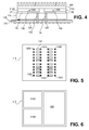
- FIG. 4 shows the connected integrated circuit structure of FIG. 2 through lines 3 - 3 ′ layer according to another embodiment.
- contact points 220 of die 210 C and die 210 D are not aligned to through-silicon vias 130 extending between package 310 and through die 110 .
- FIG. 4 shows redistribution layer 150 of, for example, a conductive material such as copper patterned, in one embodiment, on a back side of die 110 .
- FIG. 5 shows a back side surface of die 110 having through-silicon vias 130 A and 130 B extending through die 110 to the back side surface.
- FIG. 5 also shows patterned redistribution layer 150 extending laterally from each through-silicon via 130 A. In this example, through-silicon vias 130 B would be aligned with contact points of second dice 210 .
- redistribution layer 150 may be a conductive material such as copper patterned using photolithographic techniques wherein, for example, a copper material is deposited on a back side surface of die 110 followed by a mask to define redistribution layer 150 and etching to pattern the redistribution layer as fingers extending laterally from through-silicon vias 130 A to a desired position for electrical contact with contact points of second dice 210 C and 210 D. Redistribution layer 150 may be connected to contact points of dies 210 through, for example, solder connections as can through-silicon vias 130 B.
- a spacer material may be formed of, for example, a dielectric material in conjunction with the redistribution layer on a surface of die 110 or dies 210 to account for any gaps between the dies.
- FIG. 4 shows spacer material 160 formed with redistribution layer 150 on a surface of die 110 .
- FIG. 6 shows a top view of a connected integrated circuit structure of die 510 of, for example, a CPU or logic die.
- a surface e.g., a back side surface
- die 610 A and 610 B are arranged on a surface (e.g., a back side surface) of die 510 .
- die 620 having a die size (cross-sectional area) greater than die 610 A or die 610 B.
- Die 620 is, for example, SRAM memory.
- die 610 A, die 610 B and die 620 are described as memory dice, but it is appreciated that other forms of die may be used as well, such as CPU or logic dice.
- FIG. 7 shows a flow chart of a method of forming a connected integrated circuit structure.
- memory dice will be assembled on a surface, such as a back side surface of a CPU or logic die.
- a surface such as a back side surface of a CPU or logic die.
- the selection of the type of die may vary.
- the memory requirements for a connected integrated circuit structure are determined (block 710 ).
- the desired memory requirements may be one gigabyte (Gb) of DRAM memory for a connected integrated circuit structure.
- a number of memory dice are then selected such that a sum of the surface area of multiple dice approximate the surface area (e.g., a back side surface area) of a CPU logic die (block 720 ). For example, where a surface area of a CPU or logic die is 400 mm 2 , and one Gb DRAM memory chips are available having a surface area of 100 mm 2 , four DRAM memory chips (4 ⁇ 100 mm 2 ) approximates a surface area of the CPU or logic die.
- the contact points (power and I/O contact points) of the memory dice are examined and a pattern compared to a pattern of through-silicon vias desired for the CPU logic die. At that point, a determination is made whether a redistribution layer is necessary (block 730 ). If no redistribution layer is necessary, the contacts may be patterned on the back side of CPU or logic die (block 740 ). If a redistribution layer is necessary, a redistribution layer is patterned on a back side surface of a CPU or logic die and contacts established to the redistribution layer (block 750 ).
- the multiple memory dies are connected to the CPU or logic die by, for example, solder connections (block 760 ).
- the connected die stack may be connected to a substrate package including the through-silicon vias that extend to the memory dies (block 770 ).
- a heat sink and any other processing techniques typically utilized in assembling package substrates may then follow.
- FIG. 8 shows a side view of an electronic assembly including a connected integrated circuit structure that can be physically and electrically connected to a printed wiring board or printed circuit board (PCB).
- the electronic assembly can be part of an electronic system such as a computer (e.g., desktop, laptop, handheld, server, etc.), wireless communication device (e.g., cellular phone, cordless phone, pager, etc.), computer-related peripheral (e.g., printer, scanner, monitor, etc.), entertainment device (e.g., television, radio, stereo, tape and compact disc player, video cassette recorder, MP3 (motion picture experts group, audio layer 3 player, etc.), and the like.
- FIG. 8 illustrates the package is part of a desktop computer.
- FIG. 8 shows electronic assembly 800 including connected integrated circuit structure 805 physically and electrically connected to package substrate 810 .
- Package substrate 810 may be used to connect die 100 to printed circuit board 820 , such as a motherboard or other circuit board.
Abstract
Description
Claims (18)
Priority Applications (7)
| Application Number | Priority Date | Filing Date | Title |
|---|---|---|---|
| US11/613,774 US8110899B2 (en) | 2006-12-20 | 2006-12-20 | Method for incorporating existing silicon die into 3D integrated stack |
| CN2007800470113A CN101563773B (en) | 2006-12-20 | 2007-12-06 | Method for incorporating existing silicon die into 3d integrated stack |
| BRPI0722059A BRPI0722059B1 (en) | 2006-12-20 | 2007-12-06 | apparatus, method and system for incorporating existing silicon matrix into an integrated 3d stack |
| PCT/US2007/086674 WO2008079625A1 (en) | 2006-12-20 | 2007-12-06 | Method for incorporating existing silicon die into 3d integrated stack |
| DE112007003111.5T DE112007003111B4 (en) | 2006-12-20 | 2007-12-06 | Method for picking up existing silicon chips in three-dimensionally integrated stacks, device and system |
| RU2009127834/28A RU2419179C2 (en) | 2006-12-20 | 2007-12-06 | Integrated circuit device and method of making said device |
| CN201210082226.1A CN102610596B (en) | 2006-12-20 | 2007-12-06 | For existing silicon die being attached to the method in 3D integrated stack body |
Applications Claiming Priority (1)
| Application Number | Priority Date | Filing Date | Title |
|---|---|---|---|
| US11/613,774 US8110899B2 (en) | 2006-12-20 | 2006-12-20 | Method for incorporating existing silicon die into 3D integrated stack |
Publications (2)
| Publication Number | Publication Date |
|---|---|
| US20080150088A1 US20080150088A1 (en) | 2008-06-26 |
| US8110899B2 true US8110899B2 (en) | 2012-02-07 |
Family
ID=39541641
Family Applications (1)
| Application Number | Title | Priority Date | Filing Date |
|---|---|---|---|
| US11/613,774 Active 2027-12-04 US8110899B2 (en) | 2006-12-20 | 2006-12-20 | Method for incorporating existing silicon die into 3D integrated stack |
Country Status (6)
| Country | Link |
|---|---|
| US (1) | US8110899B2 (en) |
| CN (2) | CN101563773B (en) |
| BR (1) | BRPI0722059B1 (en) |
| DE (1) | DE112007003111B4 (en) |
| RU (1) | RU2419179C2 (en) |
| WO (1) | WO2008079625A1 (en) |
Cited By (21)
| Publication number | Priority date | Publication date | Assignee | Title |
|---|---|---|---|---|
| US20100099357A1 (en) * | 2008-10-20 | 2010-04-22 | Aiconn Technology Corporation | Wireless transceiver module |
| US20130044554A1 (en) * | 2011-08-17 | 2013-02-21 | Taiwan Semiconductor Manufacturing Co., Ltd. | Dram repair architecture for wide i/o dram based 2.5d/3d system chips |
| US20130179740A1 (en) * | 2009-01-23 | 2013-07-11 | Micron Technology, Inc. | Memory devices and methods for managing error regions |
| US20190273031A1 (en) * | 2018-03-05 | 2019-09-05 | Win Semiconductors Corp. | Semiconductor Device with Antenna Integrated |
| US10522516B2 (en) * | 2008-09-06 | 2019-12-31 | Broadpak Corporation | Stacking integrated circuits containing serializer and deserializer blocks using through silicon via |
| US10580757B2 (en) | 2016-10-07 | 2020-03-03 | Xcelsis Corporation | Face-to-face mounted IC dies with orthogonal top interconnect layers |
| US10580735B2 (en) | 2016-10-07 | 2020-03-03 | Xcelsis Corporation | Stacked IC structure with system level wiring on multiple sides of the IC die |
| US10586786B2 (en) | 2016-10-07 | 2020-03-10 | Xcelsis Corporation | 3D chip sharing clock interconnect layer |
| US10593667B2 (en) | 2016-10-07 | 2020-03-17 | Xcelsis Corporation | 3D chip with shielded clock lines |
| US10600691B2 (en) | 2016-10-07 | 2020-03-24 | Xcelsis Corporation | 3D chip sharing power interconnect layer |
| US10600735B2 (en) | 2016-10-07 | 2020-03-24 | Xcelsis Corporation | 3D chip sharing data bus |
| US10600780B2 (en) | 2016-10-07 | 2020-03-24 | Xcelsis Corporation | 3D chip sharing data bus circuit |
| US10607136B2 (en) | 2017-08-03 | 2020-03-31 | Xcelsis Corporation | Time borrowing between layers of a three dimensional chip stack |
| US10672745B2 (en) | 2016-10-07 | 2020-06-02 | Xcelsis Corporation | 3D processor |
| US10672743B2 (en) | 2016-10-07 | 2020-06-02 | Xcelsis Corporation | 3D Compute circuit with high density z-axis interconnects |
| US10672744B2 (en) | 2016-10-07 | 2020-06-02 | Xcelsis Corporation | 3D compute circuit with high density Z-axis interconnects |
| US10672663B2 (en) | 2016-10-07 | 2020-06-02 | Xcelsis Corporation | 3D chip sharing power circuit |
| US11289333B2 (en) | 2016-10-07 | 2022-03-29 | Xcelsis Corporation | Direct-bonded native interconnects and active base die |
| US11413865B2 (en) | 2019-02-06 | 2022-08-16 | Hewlett-Packard Development Company, L.P. | Fluid ejection devices including contact pads |
| US11487445B2 (en) * | 2016-11-22 | 2022-11-01 | Intel Corporation | Programmable integrated circuit with stacked memory die for storing configuration data |
| US11599299B2 (en) | 2019-11-19 | 2023-03-07 | Invensas Llc | 3D memory circuit |
Families Citing this family (26)
| Publication number | Priority date | Publication date | Assignee | Title |
|---|---|---|---|---|
| US7692946B2 (en) * | 2007-06-29 | 2010-04-06 | Intel Corporation | Memory array on more than one die |
| US8521979B2 (en) | 2008-05-29 | 2013-08-27 | Micron Technology, Inc. | Memory systems and methods for controlling the timing of receiving read data |
| US7979757B2 (en) | 2008-06-03 | 2011-07-12 | Micron Technology, Inc. | Method and apparatus for testing high capacity/high bandwidth memory devices |
| US8289760B2 (en) | 2008-07-02 | 2012-10-16 | Micron Technology, Inc. | Multi-mode memory device and method having stacked memory dice, a logic die and a command processing circuit and operating in direct and indirect modes |
| US7855931B2 (en) | 2008-07-21 | 2010-12-21 | Micron Technology, Inc. | Memory system and method using stacked memory device dice, and system using the memory system |
| US8756486B2 (en) * | 2008-07-02 | 2014-06-17 | Micron Technology, Inc. | Method and apparatus for repairing high capacity/high bandwidth memory devices |
| US8127204B2 (en) | 2008-08-15 | 2012-02-28 | Micron Technology, Inc. | Memory system and method using a memory device die stacked with a logic die using data encoding, and system using the memory system |
| US8082537B1 (en) * | 2009-01-28 | 2011-12-20 | Xilinx, Inc. | Method and apparatus for implementing spatially programmable through die vias in an integrated circuit |
| US7989959B1 (en) | 2009-01-29 | 2011-08-02 | Xilinx, Inc. | Method of forming stacked-die integrated circuit |
| US8987868B1 (en) | 2009-02-24 | 2015-03-24 | Xilinx, Inc. | Method and apparatus for programmable heterogeneous integration of stacked semiconductor die |
| US8421500B2 (en) * | 2009-11-30 | 2013-04-16 | International Business Machines Corporation | Integrated circuit with stacked computational units and configurable through vias |
| US9015023B2 (en) | 2010-05-05 | 2015-04-21 | Xilinx, Inc. | Device specific configuration of operating voltage |
| CN102254840A (en) * | 2010-05-18 | 2011-11-23 | 宏宝科技股份有限公司 | Semiconductor device and manufacture method thereof |
| US8525340B2 (en) * | 2010-06-11 | 2013-09-03 | Premitec, Inc. | Flexible electronic devices and related methods |
| US8492911B2 (en) | 2010-07-20 | 2013-07-23 | Lsi Corporation | Stacked interconnect heat sink |
| US8400808B2 (en) | 2010-12-16 | 2013-03-19 | Micron Technology, Inc. | Phase interpolators and push-pull buffers |
| US9256279B2 (en) | 2011-06-29 | 2016-02-09 | Rambus Inc. | Multi-element memory device with power control for individual elements |
| CN103875068B (en) * | 2011-10-17 | 2018-07-10 | 皇家飞利浦有限公司 | Through-wafer highway device and its manufacturing method |
| JP2015502663A (en) * | 2011-12-01 | 2015-01-22 | コンバーサント・インテレクチュアル・プロパティ・マネジメント・インコーポレイテッドConversant Intellectual Property Management Inc. | CPU with stacked memory |
| US9000490B2 (en) | 2013-04-19 | 2015-04-07 | Xilinx, Inc. | Semiconductor package having IC dice and voltage tuners |
| US9171597B2 (en) | 2013-08-30 | 2015-10-27 | Micron Technology, Inc. | Apparatuses and methods for providing strobe signals to memories |
| US9373588B2 (en) * | 2013-09-24 | 2016-06-21 | Intel Corporation | Stacked microelectronic dice embedded in a microelectronic substrate |
| US9559040B2 (en) | 2013-12-30 | 2017-01-31 | International Business Machines Corporation | Double-sided segmented line architecture in 3D integration |
| KR102460720B1 (en) * | 2017-11-16 | 2022-10-31 | 삼성전자주식회사 | Electronic device comprising semiconductor device package |
| FR3082656B1 (en) | 2018-06-18 | 2022-02-04 | Commissariat Energie Atomique | INTEGRATED CIRCUIT COMPRISING MACROS AND ITS MANUFACTURING METHOD |
| US11348856B2 (en) * | 2019-12-20 | 2022-05-31 | Micron Technology, Inc. | Thermal cooling element for memory devices of a memory sub-system |
Citations (73)
| Publication number | Priority date | Publication date | Assignee | Title |
|---|---|---|---|---|
| US5485039A (en) * | 1991-12-27 | 1996-01-16 | Hitachi, Ltd. | Semiconductor substrate having wiring conductors at a first main surface electrically connected to plural pins at a second main surface |
| US5702984A (en) * | 1993-09-13 | 1997-12-30 | International Business Machines Corporation | Integrated mulitchip memory module, structure and fabrication |
| US5973392A (en) * | 1997-04-02 | 1999-10-26 | Nec Corporation | Stacked carrier three-dimensional memory module and semiconductor device using the same |
| US5990564A (en) * | 1997-05-30 | 1999-11-23 | Lucent Technologies Inc. | Flip chip packaging of memory chips |
| US6025638A (en) * | 1998-06-01 | 2000-02-15 | International Business Machines Corporation | Structure for precision multichip assembly |
| US6052287A (en) * | 1997-12-09 | 2000-04-18 | Sandia Corporation | Silicon ball grid array chip carrier |
| US6255899B1 (en) * | 1999-09-01 | 2001-07-03 | International Business Machines Corporation | Method and apparatus for increasing interchip communications rates |
| US20020016021A1 (en) * | 1999-10-14 | 2002-02-07 | Sun Microsystems, Inc. | Face to face chip |
| US6348728B1 (en) * | 2000-01-28 | 2002-02-19 | Fujitsu Limited | Semiconductor device having a plurality of semiconductor elements interconnected by a redistribution layer |
| US6362525B1 (en) * | 1999-11-09 | 2002-03-26 | Cypress Semiconductor Corp. | Circuit structure including a passive element formed within a grid array substrate and method for making the same |
| US20020074637A1 (en) * | 2000-12-19 | 2002-06-20 | Intel Corporation | Stacked flip chip assemblies |
| US20020140069A1 (en) * | 2001-03-30 | 2002-10-03 | Megic Corporation | Structure and manufactruing method of chip scale package |
| US6461897B2 (en) * | 2000-02-29 | 2002-10-08 | Advanced Semiconductor Engineering, Inc. | Multichip module having a stacked chip arrangement |
| US6483043B1 (en) * | 2000-05-19 | 2002-11-19 | Eaglestone Partners I, Llc | Chip assembly with integrated power distribution between a wafer interposer and an integrated circuit chip |
| US6507115B2 (en) * | 2000-12-14 | 2003-01-14 | International Business Machines Corporation | Multi-chip integrated circuit module |
| US6563205B1 (en) * | 1995-08-16 | 2003-05-13 | Micron Technology, Inc. | Angularly offset and recessed stacked die multichip device and method of manufacture |
| US20030123240A1 (en) * | 2001-12-28 | 2003-07-03 | Medtronic Physio-Control Manufacturing Corporation | Circuit package and method for making the same |
| US6593644B2 (en) * | 2001-04-19 | 2003-07-15 | International Business Machines Corporation | System of a package fabricated on a semiconductor or dielectric wafer with wiring on one face, vias extending through the wafer, and external connections on the opposing face |
| US6620647B2 (en) * | 2000-02-03 | 2003-09-16 | Infineon Technologies Ag | Method for producing a semiconductor component with a silicon carrier substrate |
| US6642610B2 (en) * | 1999-12-20 | 2003-11-04 | Amkor Technology, Inc. | Wire bonding method and semiconductor package manufactured using the same |
| US6661086B2 (en) * | 1999-11-15 | 2003-12-09 | Infineon Technologies Ag | Three-dimensionally embodied circuit with electrically connected semiconductor chips |
| US6677668B1 (en) * | 1998-01-13 | 2004-01-13 | Paul T. Lin | Configuration for testing a substrate mounted with a most performance-demanding integrated circuit |
| US20040021139A1 (en) * | 2002-07-31 | 2004-02-05 | Jackson Timothy L. | Semiconductor dice having backside redistribution layer accessed using through-silicon vias, methods of fabrication and assemblies |
| US6696765B2 (en) * | 2001-11-19 | 2004-02-24 | Hitachi, Ltd. | Multi-chip module |
| US20040056342A1 (en) * | 2002-05-08 | 2004-03-25 | Cobbley Chad A. | Stacked die module and techniques for forming a stacked die module |
| US6717251B2 (en) * | 2000-09-28 | 2004-04-06 | Kabushiki Kaisha Toshiba | Stacked type semiconductor device |
| US20040075170A1 (en) * | 2002-10-21 | 2004-04-22 | Yinon Degani | High frequency integrated circuits |
| US6731009B1 (en) * | 2000-03-20 | 2004-05-04 | Cypress Semiconductor Corporation | Multi-die assembly |
| US20040115867A1 (en) * | 2001-11-01 | 2004-06-17 | Kazutaka Shibata | Semiconductor device and method for manufacturing same |
| US6798049B1 (en) * | 1999-08-24 | 2004-09-28 | Amkor Technology Inc. | Semiconductor package and method for fabricating the same |
| US6815808B2 (en) * | 2000-10-10 | 2004-11-09 | Sanyo Electric, Co., Ltd. | Hollow airtight semiconductor device package |
| US20050127490A1 (en) * | 2003-12-16 | 2005-06-16 | Black Bryan P. | Multi-die processor |
| US6911730B1 (en) * | 2003-03-03 | 2005-06-28 | Xilinx, Inc. | Multi-chip module including embedded transistors within the substrate |
| US6929976B2 (en) * | 2001-06-21 | 2005-08-16 | Ati Technologies, Inc. | Multi-die module and method thereof |
| US6961231B1 (en) * | 2002-12-06 | 2005-11-01 | Xilinx, Inc. | Interposer providing low-inductance decoupling capacitance for a packaged integrated circuit |
| US20060043569A1 (en) * | 2004-08-27 | 2006-03-02 | Benson Peter A | Low temperature methods of forming back side redistribution layers in association with through wafer interconnects, semiconductor devices including same, and assemblies |
| US20060077749A1 (en) * | 2004-10-07 | 2006-04-13 | Cheng-Hsien Kuo | Memory card structure and manufacturing method thereof |
| US7030470B1 (en) * | 2004-05-11 | 2006-04-18 | Sun Microsystems, Inc. | Using chip lamination to couple an integrated circuit with a microstrip transmission line |
| US7035113B2 (en) * | 2003-01-30 | 2006-04-25 | Endicott Interconnect Technologies, Inc. | Multi-chip electronic package having laminate carrier and method of making same |
| US7045892B2 (en) * | 2003-07-04 | 2006-05-16 | Samsung Electronics Co., Ltd. | Stack package of semiconductor device |
| US7058247B2 (en) * | 2003-12-17 | 2006-06-06 | International Business Machines Corporation | Silicon carrier for optical interconnect modules |
| US7061092B2 (en) * | 1999-02-01 | 2006-06-13 | Micron Technology, Inc. | High-density modularity for ICS |
| US7060601B2 (en) * | 2003-12-17 | 2006-06-13 | Tru-Si Technologies, Inc. | Packaging substrates for integrated circuits and soldering methods |
| US7064005B2 (en) * | 2001-05-14 | 2006-06-20 | Sony Corporation | Semiconductor apparatus and method of manufacturing same |
| US7078818B2 (en) * | 2000-09-07 | 2006-07-18 | Matsushita Electric Industrial Co., Ltd. | Semiconductor device |
| US20060202317A1 (en) * | 2005-03-14 | 2006-09-14 | Farid Barakat | Method for MCP packaging for balanced performance |
| US7109068B2 (en) | 2004-08-31 | 2006-09-19 | Micron Technology, Inc. | Through-substrate interconnect fabrication methods |
| US7112887B2 (en) * | 2002-03-28 | 2006-09-26 | Intel Corporation | Integrated circuit die and an electronic assembly having a three-dimensional interconnection scheme |
| US7132753B1 (en) * | 2003-11-10 | 2006-11-07 | Amkor Technology, Inc. | Stacked die assembly having semiconductor die overhanging support |
| US20060267171A1 (en) * | 2001-08-21 | 2006-11-30 | Micron Technology, Inc. | Semiconductor device modules, semiconductor devices, and microelectronic devices |
| US20060275957A1 (en) * | 2001-09-28 | 2006-12-07 | Rohm Co., Ltd. | Semiconductor device |
| US20060278979A1 (en) * | 2005-06-09 | 2006-12-14 | Intel Corporation | Die stacking recessed pad wafer design |
| US7161810B2 (en) * | 2003-01-30 | 2007-01-09 | Endicott Interconnect Technologies, Inc. | Stacked chip electronic package having laminate carrier and method of making same |
| US20070045788A1 (en) * | 2005-08-31 | 2007-03-01 | Takehiro Suzuki | Stacking semiconductor device and production method thereof |
| US7202554B1 (en) * | 2004-08-19 | 2007-04-10 | Amkor Technology, Inc. | Semiconductor package and its manufacturing method |
| US20070126085A1 (en) * | 2005-12-02 | 2007-06-07 | Nec Electronics Corporation | Semiconductor device and method of manufacturing the same |
| US20070138653A1 (en) * | 2005-12-15 | 2007-06-21 | International Business Machines Corporation | Method and power control structure for managing plurality of voltage islands |
| US7239012B2 (en) * | 2001-10-30 | 2007-07-03 | Irvine Sensors Corp. | Three-dimensional module comprised of layers containing IC chips with overlying interconnect layers |
| US20070152313A1 (en) * | 2005-12-29 | 2007-07-05 | Shanggar Periaman | Stacked die semiconductor package |
| US7242100B2 (en) * | 1997-10-06 | 2007-07-10 | Rohm Co., Ltd. | Method for manufacturing semiconductor device with plural semiconductor chips |
| US7247932B1 (en) * | 2000-05-19 | 2007-07-24 | Megica Corporation | Chip package with capacitor |
| US20070294479A1 (en) * | 2006-06-16 | 2007-12-20 | International Business Machines Corporation | Method for achieving very high bandwidth between the levels of a cache hierarchy in 3-Dimensional structures, and a 3-dimensional structure resulting therefrom |
| US20080054489A1 (en) * | 2006-08-31 | 2008-03-06 | Micron Technology, Inc. | Distributed semiconductor device methods, apparatus, and systems |
| US20080083975A1 (en) * | 2006-10-09 | 2008-04-10 | Taiwan Semiconductor Manufacturing Co., Ltd. | Stacked structures and methods of fabricating stacked structures |
| US7402442B2 (en) * | 2005-12-21 | 2008-07-22 | International Business Machines Corporation | Physically highly secure multi-chip assembly |
| US7486525B2 (en) * | 2006-08-04 | 2009-02-03 | International Business Machines Corporation | Temporary chip attach carrier |
| US7498668B2 (en) * | 2005-10-27 | 2009-03-03 | Panasonic Corporation | Stacked semiconductor device and lower module of stacked semiconductor device |
| US7586183B2 (en) * | 2005-04-19 | 2009-09-08 | Panasonic Corporation | Multilevel semiconductor module and method for fabricating the same |
| US7595559B2 (en) * | 2004-07-27 | 2009-09-29 | Samsung Electronics Co., Ltd. | Integrated circuit chip having pass-through vias therein that extend between multiple integrated circuits on the chip |
| US20100032820A1 (en) * | 2008-08-06 | 2010-02-11 | Michael Bruennert | Stacked Memory Module |
| US7692278B2 (en) * | 2006-12-20 | 2010-04-06 | Intel Corporation | Stacked-die packages with silicon vias and surface activated bonding |
| US7746656B2 (en) * | 2005-05-16 | 2010-06-29 | Stats Chippac Ltd. | Offset integrated circuit package-on-package stacking system |
| US7893540B2 (en) * | 2005-06-30 | 2011-02-22 | Elpida Memory, Inc. | Semiconductor memory device and manufacturing method thereof |
Family Cites Families (4)
| Publication number | Priority date | Publication date | Assignee | Title |
|---|---|---|---|---|
| US6268660B1 (en) | 1999-03-05 | 2001-07-31 | International Business Machines Corporation | Silicon packaging with through wafer interconnects |
| CN1729050A (en) * | 2002-12-20 | 2006-02-01 | 本田技研工业株式会社 | Platinum-ruthenium containing catalyst formulations for hydrogen generation |
| US7475175B2 (en) * | 2003-03-17 | 2009-01-06 | Hewlett-Packard Development Company, L.P. | Multi-processor module |
| US7317256B2 (en) * | 2005-06-01 | 2008-01-08 | Intel Corporation | Electronic packaging including die with through silicon via |
-
2006
- 2006-12-20 US US11/613,774 patent/US8110899B2/en active Active
-
2007
- 2007-12-06 CN CN2007800470113A patent/CN101563773B/en not_active Expired - Fee Related
- 2007-12-06 CN CN201210082226.1A patent/CN102610596B/en not_active Expired - Fee Related
- 2007-12-06 BR BRPI0722059A patent/BRPI0722059B1/en not_active IP Right Cessation
- 2007-12-06 RU RU2009127834/28A patent/RU2419179C2/en not_active IP Right Cessation
- 2007-12-06 WO PCT/US2007/086674 patent/WO2008079625A1/en active Application Filing
- 2007-12-06 DE DE112007003111.5T patent/DE112007003111B4/en active Active
Patent Citations (77)
| Publication number | Priority date | Publication date | Assignee | Title |
|---|---|---|---|---|
| US5485039A (en) * | 1991-12-27 | 1996-01-16 | Hitachi, Ltd. | Semiconductor substrate having wiring conductors at a first main surface electrically connected to plural pins at a second main surface |
| US5702984A (en) * | 1993-09-13 | 1997-12-30 | International Business Machines Corporation | Integrated mulitchip memory module, structure and fabrication |
| US6563205B1 (en) * | 1995-08-16 | 2003-05-13 | Micron Technology, Inc. | Angularly offset and recessed stacked die multichip device and method of manufacture |
| US5973392A (en) * | 1997-04-02 | 1999-10-26 | Nec Corporation | Stacked carrier three-dimensional memory module and semiconductor device using the same |
| US5990564A (en) * | 1997-05-30 | 1999-11-23 | Lucent Technologies Inc. | Flip chip packaging of memory chips |
| US7242100B2 (en) * | 1997-10-06 | 2007-07-10 | Rohm Co., Ltd. | Method for manufacturing semiconductor device with plural semiconductor chips |
| US6052287A (en) * | 1997-12-09 | 2000-04-18 | Sandia Corporation | Silicon ball grid array chip carrier |
| US6677668B1 (en) * | 1998-01-13 | 2004-01-13 | Paul T. Lin | Configuration for testing a substrate mounted with a most performance-demanding integrated circuit |
| US6025638A (en) * | 1998-06-01 | 2000-02-15 | International Business Machines Corporation | Structure for precision multichip assembly |
| US7061092B2 (en) * | 1999-02-01 | 2006-06-13 | Micron Technology, Inc. | High-density modularity for ICS |
| US6798049B1 (en) * | 1999-08-24 | 2004-09-28 | Amkor Technology Inc. | Semiconductor package and method for fabricating the same |
| US6255899B1 (en) * | 1999-09-01 | 2001-07-03 | International Business Machines Corporation | Method and apparatus for increasing interchip communications rates |
| US20020016021A1 (en) * | 1999-10-14 | 2002-02-07 | Sun Microsystems, Inc. | Face to face chip |
| US6362525B1 (en) * | 1999-11-09 | 2002-03-26 | Cypress Semiconductor Corp. | Circuit structure including a passive element formed within a grid array substrate and method for making the same |
| US6661086B2 (en) * | 1999-11-15 | 2003-12-09 | Infineon Technologies Ag | Three-dimensionally embodied circuit with electrically connected semiconductor chips |
| US6642610B2 (en) * | 1999-12-20 | 2003-11-04 | Amkor Technology, Inc. | Wire bonding method and semiconductor package manufactured using the same |
| US6348728B1 (en) * | 2000-01-28 | 2002-02-19 | Fujitsu Limited | Semiconductor device having a plurality of semiconductor elements interconnected by a redistribution layer |
| US6620647B2 (en) * | 2000-02-03 | 2003-09-16 | Infineon Technologies Ag | Method for producing a semiconductor component with a silicon carrier substrate |
| US6461897B2 (en) * | 2000-02-29 | 2002-10-08 | Advanced Semiconductor Engineering, Inc. | Multichip module having a stacked chip arrangement |
| US6731009B1 (en) * | 2000-03-20 | 2004-05-04 | Cypress Semiconductor Corporation | Multi-die assembly |
| US7247932B1 (en) * | 2000-05-19 | 2007-07-24 | Megica Corporation | Chip package with capacitor |
| US6483043B1 (en) * | 2000-05-19 | 2002-11-19 | Eaglestone Partners I, Llc | Chip assembly with integrated power distribution between a wafer interposer and an integrated circuit chip |
| US7078818B2 (en) * | 2000-09-07 | 2006-07-18 | Matsushita Electric Industrial Co., Ltd. | Semiconductor device |
| US6717251B2 (en) * | 2000-09-28 | 2004-04-06 | Kabushiki Kaisha Toshiba | Stacked type semiconductor device |
| US6815808B2 (en) * | 2000-10-10 | 2004-11-09 | Sanyo Electric, Co., Ltd. | Hollow airtight semiconductor device package |
| US6507115B2 (en) * | 2000-12-14 | 2003-01-14 | International Business Machines Corporation | Multi-chip integrated circuit module |
| US20020074637A1 (en) * | 2000-12-19 | 2002-06-20 | Intel Corporation | Stacked flip chip assemblies |
| US20020140069A1 (en) * | 2001-03-30 | 2002-10-03 | Megic Corporation | Structure and manufactruing method of chip scale package |
| US6593644B2 (en) * | 2001-04-19 | 2003-07-15 | International Business Machines Corporation | System of a package fabricated on a semiconductor or dielectric wafer with wiring on one face, vias extending through the wafer, and external connections on the opposing face |
| US7064005B2 (en) * | 2001-05-14 | 2006-06-20 | Sony Corporation | Semiconductor apparatus and method of manufacturing same |
| US6929976B2 (en) * | 2001-06-21 | 2005-08-16 | Ati Technologies, Inc. | Multi-die module and method thereof |
| US20060267171A1 (en) * | 2001-08-21 | 2006-11-30 | Micron Technology, Inc. | Semiconductor device modules, semiconductor devices, and microelectronic devices |
| US20060275957A1 (en) * | 2001-09-28 | 2006-12-07 | Rohm Co., Ltd. | Semiconductor device |
| US7239012B2 (en) * | 2001-10-30 | 2007-07-03 | Irvine Sensors Corp. | Three-dimensional module comprised of layers containing IC chips with overlying interconnect layers |
| US20040115867A1 (en) * | 2001-11-01 | 2004-06-17 | Kazutaka Shibata | Semiconductor device and method for manufacturing same |
| US6696765B2 (en) * | 2001-11-19 | 2004-02-24 | Hitachi, Ltd. | Multi-chip module |
| US20030123240A1 (en) * | 2001-12-28 | 2003-07-03 | Medtronic Physio-Control Manufacturing Corporation | Circuit package and method for making the same |
| US7112887B2 (en) * | 2002-03-28 | 2006-09-26 | Intel Corporation | Integrated circuit die and an electronic assembly having a three-dimensional interconnection scheme |
| US20040056342A1 (en) * | 2002-05-08 | 2004-03-25 | Cobbley Chad A. | Stacked die module and techniques for forming a stacked die module |
| US20040021139A1 (en) * | 2002-07-31 | 2004-02-05 | Jackson Timothy L. | Semiconductor dice having backside redistribution layer accessed using through-silicon vias, methods of fabrication and assemblies |
| US20040075170A1 (en) * | 2002-10-21 | 2004-04-22 | Yinon Degani | High frequency integrated circuits |
| US6961231B1 (en) * | 2002-12-06 | 2005-11-01 | Xilinx, Inc. | Interposer providing low-inductance decoupling capacitance for a packaged integrated circuit |
| US7035113B2 (en) * | 2003-01-30 | 2006-04-25 | Endicott Interconnect Technologies, Inc. | Multi-chip electronic package having laminate carrier and method of making same |
| US7161810B2 (en) * | 2003-01-30 | 2007-01-09 | Endicott Interconnect Technologies, Inc. | Stacked chip electronic package having laminate carrier and method of making same |
| US6911730B1 (en) * | 2003-03-03 | 2005-06-28 | Xilinx, Inc. | Multi-chip module including embedded transistors within the substrate |
| US7045892B2 (en) * | 2003-07-04 | 2006-05-16 | Samsung Electronics Co., Ltd. | Stack package of semiconductor device |
| US7132753B1 (en) * | 2003-11-10 | 2006-11-07 | Amkor Technology, Inc. | Stacked die assembly having semiconductor die overhanging support |
| US20050127490A1 (en) * | 2003-12-16 | 2005-06-16 | Black Bryan P. | Multi-die processor |
| US7058247B2 (en) * | 2003-12-17 | 2006-06-06 | International Business Machines Corporation | Silicon carrier for optical interconnect modules |
| US7060601B2 (en) * | 2003-12-17 | 2006-06-13 | Tru-Si Technologies, Inc. | Packaging substrates for integrated circuits and soldering methods |
| US7030470B1 (en) * | 2004-05-11 | 2006-04-18 | Sun Microsystems, Inc. | Using chip lamination to couple an integrated circuit with a microstrip transmission line |
| US7595559B2 (en) * | 2004-07-27 | 2009-09-29 | Samsung Electronics Co., Ltd. | Integrated circuit chip having pass-through vias therein that extend between multiple integrated circuits on the chip |
| US7202554B1 (en) * | 2004-08-19 | 2007-04-10 | Amkor Technology, Inc. | Semiconductor package and its manufacturing method |
| US20060043569A1 (en) * | 2004-08-27 | 2006-03-02 | Benson Peter A | Low temperature methods of forming back side redistribution layers in association with through wafer interconnects, semiconductor devices including same, and assemblies |
| US7109068B2 (en) | 2004-08-31 | 2006-09-19 | Micron Technology, Inc. | Through-substrate interconnect fabrication methods |
| US20060077749A1 (en) * | 2004-10-07 | 2006-04-13 | Cheng-Hsien Kuo | Memory card structure and manufacturing method thereof |
| US20060202317A1 (en) * | 2005-03-14 | 2006-09-14 | Farid Barakat | Method for MCP packaging for balanced performance |
| US7586183B2 (en) * | 2005-04-19 | 2009-09-08 | Panasonic Corporation | Multilevel semiconductor module and method for fabricating the same |
| US7746656B2 (en) * | 2005-05-16 | 2010-06-29 | Stats Chippac Ltd. | Offset integrated circuit package-on-package stacking system |
| US20060278979A1 (en) * | 2005-06-09 | 2006-12-14 | Intel Corporation | Die stacking recessed pad wafer design |
| US7893540B2 (en) * | 2005-06-30 | 2011-02-22 | Elpida Memory, Inc. | Semiconductor memory device and manufacturing method thereof |
| US20070045788A1 (en) * | 2005-08-31 | 2007-03-01 | Takehiro Suzuki | Stacking semiconductor device and production method thereof |
| US7498668B2 (en) * | 2005-10-27 | 2009-03-03 | Panasonic Corporation | Stacked semiconductor device and lower module of stacked semiconductor device |
| US20070126085A1 (en) * | 2005-12-02 | 2007-06-07 | Nec Electronics Corporation | Semiconductor device and method of manufacturing the same |
| US20070138653A1 (en) * | 2005-12-15 | 2007-06-21 | International Business Machines Corporation | Method and power control structure for managing plurality of voltage islands |
| US7768005B2 (en) * | 2005-12-21 | 2010-08-03 | International Business Machines Corporation | Physically highly secure multi-chip assembly |
| US7402442B2 (en) * | 2005-12-21 | 2008-07-22 | International Business Machines Corporation | Physically highly secure multi-chip assembly |
| US20070152313A1 (en) * | 2005-12-29 | 2007-07-05 | Shanggar Periaman | Stacked die semiconductor package |
| US7279795B2 (en) * | 2005-12-29 | 2007-10-09 | Intel Corporation | Stacked die semiconductor package |
| US7518225B2 (en) * | 2006-06-16 | 2009-04-14 | International Business Machines Corporation | Chip system architecture for performance enhancement, power reduction and cost reduction |
| US20070294479A1 (en) * | 2006-06-16 | 2007-12-20 | International Business Machines Corporation | Method for achieving very high bandwidth between the levels of a cache hierarchy in 3-Dimensional structures, and a 3-dimensional structure resulting therefrom |
| US7486525B2 (en) * | 2006-08-04 | 2009-02-03 | International Business Machines Corporation | Temporary chip attach carrier |
| US20080054489A1 (en) * | 2006-08-31 | 2008-03-06 | Micron Technology, Inc. | Distributed semiconductor device methods, apparatus, and systems |
| US7514775B2 (en) * | 2006-10-09 | 2009-04-07 | Taiwan Semiconductor Manufacturing Co., Ltd. | Stacked structures and methods of fabricating stacked structures |
| US20080083975A1 (en) * | 2006-10-09 | 2008-04-10 | Taiwan Semiconductor Manufacturing Co., Ltd. | Stacked structures and methods of fabricating stacked structures |
| US7692278B2 (en) * | 2006-12-20 | 2010-04-06 | Intel Corporation | Stacked-die packages with silicon vias and surface activated bonding |
| US20100032820A1 (en) * | 2008-08-06 | 2010-02-11 | Michael Bruennert | Stacked Memory Module |
Non-Patent Citations (5)
| Title |
|---|
| Intel Corporation, "PCT Search Report and Written Opinion mailed May 13, 2008," PCT/US/2007086674. |
| Intel Corporation, Office Action dated Apr. 19, 2011 for Chinese Application No. 200780047011.3. |
| Intel Corporation, Office Action dated Feb. 12, 2010 for Chinese Application No. 200780047011.3. |
| Intel Corporation, Official Action from Patent Office of Russia Federation dated Jul. 12, 2010 for RU2009127834/28(038666). |
| Schaper, Leonard W., et al,, "Architectural Implications and Process Development of 3-D VLSI Z-Axis Interconnects Using Through Silicon Vias", IEEE Transactions on Advanced Packaging, vol. 28, No. 3, Aug. 2005 , 356-364. |
Cited By (45)
| Publication number | Priority date | Publication date | Assignee | Title |
|---|---|---|---|---|
| US10522516B2 (en) * | 2008-09-06 | 2019-12-31 | Broadpak Corporation | Stacking integrated circuits containing serializer and deserializer blocks using through silicon via |
| US20100099357A1 (en) * | 2008-10-20 | 2010-04-22 | Aiconn Technology Corporation | Wireless transceiver module |
| US8478197B2 (en) * | 2008-10-20 | 2013-07-02 | Accton Technology Corporation | Wireless transceiver module |
| US20130179740A1 (en) * | 2009-01-23 | 2013-07-11 | Micron Technology, Inc. | Memory devices and methods for managing error regions |
| US8990647B2 (en) * | 2009-01-23 | 2015-03-24 | Micron Technology, Inc. | Memory devices and methods for managing error regions |
| US9953724B2 (en) | 2009-01-23 | 2018-04-24 | Micron Technology, Inc. | Memory devices and methods for managing error regions |
| US10347356B2 (en) | 2009-01-23 | 2019-07-09 | Micron Technology, Inc. | Memory devices and methods for managing error regions |
| US11915774B2 (en) | 2009-01-23 | 2024-02-27 | Micron Technology, Inc. | Memory devices and methods for managing error regions |
| US11145384B2 (en) | 2009-01-23 | 2021-10-12 | Micron Technology, Inc. | Memory devices and methods for managing error regions |
| US20130044554A1 (en) * | 2011-08-17 | 2013-02-21 | Taiwan Semiconductor Manufacturing Co., Ltd. | Dram repair architecture for wide i/o dram based 2.5d/3d system chips |
| US8873320B2 (en) * | 2011-08-17 | 2014-10-28 | Taiwan Semiconductor Manufacturing Co., Ltd. | DRAM repair architecture for wide I/O DRAM based 2.5D/3D system chips |
| US10600780B2 (en) | 2016-10-07 | 2020-03-24 | Xcelsis Corporation | 3D chip sharing data bus circuit |
| US11824042B2 (en) | 2016-10-07 | 2023-11-21 | Xcelsis Corporation | 3D chip sharing data bus |
| US10593667B2 (en) | 2016-10-07 | 2020-03-17 | Xcelsis Corporation | 3D chip with shielded clock lines |
| US10600691B2 (en) | 2016-10-07 | 2020-03-24 | Xcelsis Corporation | 3D chip sharing power interconnect layer |
| US10600735B2 (en) | 2016-10-07 | 2020-03-24 | Xcelsis Corporation | 3D chip sharing data bus |
| US10580735B2 (en) | 2016-10-07 | 2020-03-03 | Xcelsis Corporation | Stacked IC structure with system level wiring on multiple sides of the IC die |
| US11881454B2 (en) | 2016-10-07 | 2024-01-23 | Adeia Semiconductor Inc. | Stacked IC structure with orthogonal interconnect layers |
| US10672745B2 (en) | 2016-10-07 | 2020-06-02 | Xcelsis Corporation | 3D processor |
| US10672743B2 (en) | 2016-10-07 | 2020-06-02 | Xcelsis Corporation | 3D Compute circuit with high density z-axis interconnects |
| US10672744B2 (en) | 2016-10-07 | 2020-06-02 | Xcelsis Corporation | 3D compute circuit with high density Z-axis interconnects |
| US10672663B2 (en) | 2016-10-07 | 2020-06-02 | Xcelsis Corporation | 3D chip sharing power circuit |
| US10586786B2 (en) | 2016-10-07 | 2020-03-10 | Xcelsis Corporation | 3D chip sharing clock interconnect layer |
| US11823906B2 (en) | 2016-10-07 | 2023-11-21 | Xcelsis Corporation | Direct-bonded native interconnects and active base die |
| US11557516B2 (en) | 2016-10-07 | 2023-01-17 | Adeia Semiconductor Inc. | 3D chip with shared clock distribution network |
| US11152336B2 (en) | 2016-10-07 | 2021-10-19 | Xcelsis Corporation | 3D processor having stacked integrated circuit die |
| US10886177B2 (en) | 2016-10-07 | 2021-01-05 | Xcelsis Corporation | 3D chip with shared clock distribution network |
| US10892252B2 (en) | 2016-10-07 | 2021-01-12 | Xcelsis Corporation | Face-to-face mounted IC dies with orthogonal top interconnect layers |
| US10950547B2 (en) | 2016-10-07 | 2021-03-16 | Xcelsis Corporation | Stacked IC structure with system level wiring on multiple sides of the IC die |
| US11289333B2 (en) | 2016-10-07 | 2022-03-29 | Xcelsis Corporation | Direct-bonded native interconnects and active base die |
| US10978348B2 (en) | 2016-10-07 | 2021-04-13 | Xcelsis Corporation | 3D chip sharing power interconnect layer |
| US10580757B2 (en) | 2016-10-07 | 2020-03-03 | Xcelsis Corporation | Face-to-face mounted IC dies with orthogonal top interconnect layers |
| US11487445B2 (en) * | 2016-11-22 | 2022-11-01 | Intel Corporation | Programmable integrated circuit with stacked memory die for storing configuration data |
| US11176450B2 (en) | 2017-08-03 | 2021-11-16 | Xcelsis Corporation | Three dimensional circuit implementing machine trained network |
| US10970627B2 (en) | 2017-08-03 | 2021-04-06 | Xcelsis Corporation | Time borrowing between layers of a three dimensional chip stack |
| US10762420B2 (en) | 2017-08-03 | 2020-09-01 | Xcelsis Corporation | Self repairing neural network |
| US10719762B2 (en) | 2017-08-03 | 2020-07-21 | Xcelsis Corporation | Three dimensional chip structure implementing machine trained network |
| US11790219B2 (en) | 2017-08-03 | 2023-10-17 | Adeia Semiconductor Inc. | Three dimensional circuit implementing machine trained network |
| US10607136B2 (en) | 2017-08-03 | 2020-03-31 | Xcelsis Corporation | Time borrowing between layers of a three dimensional chip stack |
| US10714409B2 (en) | 2018-03-05 | 2020-07-14 | Win Semiconductors Corp. | Semiconductor device with antenna integrated |
| US10679924B2 (en) * | 2018-03-05 | 2020-06-09 | Win Semiconductors Corp. | Semiconductor device with antenna integrated |
| US20190273031A1 (en) * | 2018-03-05 | 2019-09-05 | Win Semiconductors Corp. | Semiconductor Device with Antenna Integrated |
| US11413865B2 (en) | 2019-02-06 | 2022-08-16 | Hewlett-Packard Development Company, L.P. | Fluid ejection devices including contact pads |
| US11639055B2 (en) | 2019-02-06 | 2023-05-02 | Hewlett-Packard Development Company, L.P. | Fluid ejection devices including contact pads |
| US11599299B2 (en) | 2019-11-19 | 2023-03-07 | Invensas Llc | 3D memory circuit |
Also Published As
| Publication number | Publication date |
|---|---|
| CN102610596B (en) | 2015-09-16 |
| CN101563773B (en) | 2012-05-30 |
| BRPI0722059B1 (en) | 2018-10-09 |
| DE112007003111B4 (en) | 2020-06-18 |
| CN102610596A (en) | 2012-07-25 |
| RU2009127834A (en) | 2011-01-27 |
| RU2419179C2 (en) | 2011-05-20 |
| CN101563773A (en) | 2009-10-21 |
| BRPI0722059A2 (en) | 2014-04-01 |
| US20080150088A1 (en) | 2008-06-26 |
| WO2008079625A1 (en) | 2008-07-03 |
| DE112007003111T5 (en) | 2009-11-05 |
Similar Documents
| Publication | Publication Date | Title |
|---|---|---|
| US8110899B2 (en) | Method for incorporating existing silicon die into 3D integrated stack | |
| US11676902B2 (en) | Semiconductor package including interposer | |
| US11257801B2 (en) | Stacked semiconductor package having mold vias and method for manufacturing the same | |
| US9607947B2 (en) | Reliable microstrip routing for electronics components | |
| US7554203B2 (en) | Electronic assembly with stacked IC's using two or more different connection technologies and methods of manufacture | |
| KR101413220B1 (en) | Semiconductor package having interposer and method for manufacturing semiconductor package | |
| TWI436469B (en) | Improved electrical connections for multichip modules | |
| US20170207201A1 (en) | Method for fabricating fan-out wafer level package and fan-out wafer level package fabricated thereby | |
| US20170373010A1 (en) | Package-on-package type semiconductor device including fan-out memory package | |
| US20110244634A1 (en) | Semiconductor package and methods of manufacturing the same | |
| TW201637166A (en) | Semiconductor packages with interposers and methods of manufacturing the same | |
| JP2004349694A (en) | Interconnection method for integrated circuits | |
| KR20120038811A (en) | Semiconductor devices and methods of fabricating the same | |
| US20220052021A1 (en) | Semiconductor assemblies with redistribution structures for die stack signal routing | |
| US8980689B2 (en) | Method of fabricating semiconductor multi-chip stack packages | |
| US9620492B2 (en) | Package-on-package type stack package and method for manufacturing the same | |
| JP2004273706A (en) | Electronic circuit device | |
| US11562987B2 (en) | Semiconductor devices with multiple substrates and die stacks | |
| TW201919186A (en) | Bumpless fan-out chip stacking structure and method for fabricating the same | |
| KR20130106634A (en) | Semiconductor package, electronic system and manufacturing method for the same | |
| CN116313852A (en) | Multi-chip packaging structure, manufacturing method thereof and wafer-level packaging method |
Legal Events
| Date | Code | Title | Description |
|---|---|---|---|
| AS | Assignment |
Owner name: INTEL CORPORATION, CALIFORNIA Free format text: ASSIGNMENT OF ASSIGNORS INTEREST;ASSIGNORS:REED, PAUL A.;BLACK, BRYAN P.;REEL/FRAME:021419/0329 Effective date: 20061218 |
|
| FEPP | Fee payment procedure |
Free format text: PAYOR NUMBER ASSIGNED (ORIGINAL EVENT CODE: ASPN); ENTITY STATUS OF PATENT OWNER: LARGE ENTITY |
|
| STCF | Information on status: patent grant |
Free format text: PATENTED CASE |
|
| FPAY | Fee payment |
Year of fee payment: 4 |
|
| MAFP | Maintenance fee payment |
Free format text: PAYMENT OF MAINTENANCE FEE, 8TH YEAR, LARGE ENTITY (ORIGINAL EVENT CODE: M1552); ENTITY STATUS OF PATENT OWNER: LARGE ENTITY Year of fee payment: 8 |
|
| MAFP | Maintenance fee payment |
Free format text: PAYMENT OF MAINTENANCE FEE, 12TH YEAR, LARGE ENTITY (ORIGINAL EVENT CODE: M1553); ENTITY STATUS OF PATENT OWNER: LARGE ENTITY Year of fee payment: 12 |