US8110765B2 - Electroluminescent lamp membrane switch - Google Patents
Electroluminescent lamp membrane switch Download PDFInfo
- Publication number
- US8110765B2 US8110765B2 US11/452,441 US45244106A US8110765B2 US 8110765 B2 US8110765 B2 US 8110765B2 US 45244106 A US45244106 A US 45244106A US 8110765 B2 US8110765 B2 US 8110765B2
- Authority
- US
- United States
- Prior art keywords
- layer
- switch
- membrane switch
- electroluminescent lamp
- lamp
- Prior art date
- Legal status (The legal status is an assumption and is not a legal conclusion. Google has not performed a legal analysis and makes no representation as to the accuracy of the status listed.)
- Expired - Fee Related, expires
Links
- 239000012528 membrane Substances 0.000 title claims abstract description 52
- 239000000758 substrate Substances 0.000 claims abstract description 38
- BQCADISMDOOEFD-UHFFFAOYSA-N Silver Chemical compound [Ag] BQCADISMDOOEFD-UHFFFAOYSA-N 0.000 claims description 10
- 229920000642 polymer Polymers 0.000 claims description 10
- 150000001875 compounds Chemical class 0.000 claims description 8
- 239000011347 resin Substances 0.000 claims description 7
- 229920005989 resin Polymers 0.000 claims description 7
- 229910052709 silver Inorganic materials 0.000 claims description 7
- 239000004332 silver Substances 0.000 claims description 7
- OKTJSMMVPCPJKN-UHFFFAOYSA-N Carbon Chemical compound [C] OKTJSMMVPCPJKN-UHFFFAOYSA-N 0.000 claims description 6
- XEEYBQQBJWHFJM-UHFFFAOYSA-N Iron Chemical compound [Fe] XEEYBQQBJWHFJM-UHFFFAOYSA-N 0.000 claims description 6
- 239000002245 particle Substances 0.000 claims description 6
- AMGQUBHHOARCQH-UHFFFAOYSA-N indium;oxotin Chemical compound [In].[Sn]=O AMGQUBHHOARCQH-UHFFFAOYSA-N 0.000 claims description 4
- 229910001209 Low-carbon steel Inorganic materials 0.000 claims description 3
- 229920001971 elastomer Polymers 0.000 claims description 3
- 229910052738 indium Inorganic materials 0.000 claims description 3
- APFVFJFRJDLVQX-UHFFFAOYSA-N indium atom Chemical compound [In] APFVFJFRJDLVQX-UHFFFAOYSA-N 0.000 claims description 3
- 229910052742 iron Inorganic materials 0.000 claims description 3
- 229910021392 nanocarbon Inorganic materials 0.000 claims description 3
- 239000000843 powder Substances 0.000 claims description 3
- RYGMFSIKBFXOCR-UHFFFAOYSA-N Copper Chemical compound [Cu] RYGMFSIKBFXOCR-UHFFFAOYSA-N 0.000 claims 2
- 229910052802 copper Inorganic materials 0.000 claims 2
- 239000010949 copper Substances 0.000 claims 2
- 230000008859 change Effects 0.000 abstract description 8
- 238000007639 printing Methods 0.000 abstract description 7
- 239000010410 layer Substances 0.000 description 134
- 239000000976 ink Substances 0.000 description 16
- 238000000034 method Methods 0.000 description 16
- 238000005520 cutting process Methods 0.000 description 11
- 230000008569 process Effects 0.000 description 11
- 125000006850 spacer group Chemical group 0.000 description 11
- 238000003475 lamination Methods 0.000 description 10
- 238000010276 construction Methods 0.000 description 7
- 238000010924 continuous production Methods 0.000 description 7
- 239000012939 laminating adhesive Substances 0.000 description 7
- 238000004519 manufacturing process Methods 0.000 description 7
- 229910052751 metal Inorganic materials 0.000 description 6
- 239000002184 metal Substances 0.000 description 6
- 239000012790 adhesive layer Substances 0.000 description 5
- 229920000515 polycarbonate Polymers 0.000 description 5
- 239000004417 polycarbonate Substances 0.000 description 5
- 229920000728 polyester Polymers 0.000 description 5
- 230000009467 reduction Effects 0.000 description 5
- 230000008030 elimination Effects 0.000 description 4
- 238000003379 elimination reaction Methods 0.000 description 4
- 229920002635 polyurethane Polymers 0.000 description 4
- 239000004814 polyurethane Substances 0.000 description 4
- 239000000853 adhesive Substances 0.000 description 3
- 230000001070 adhesive effect Effects 0.000 description 3
- JRPBQTZRNDNNOP-UHFFFAOYSA-N barium titanate Chemical compound [Ba+2].[Ba+2].[O-][Ti]([O-])([O-])[O-] JRPBQTZRNDNNOP-UHFFFAOYSA-N 0.000 description 3
- 229910002113 barium titanate Inorganic materials 0.000 description 3
- 229910002804 graphite Inorganic materials 0.000 description 3
- 239000010439 graphite Substances 0.000 description 3
- OAICVXFJPJFONN-UHFFFAOYSA-N Phosphorus Chemical compound [P] OAICVXFJPJFONN-UHFFFAOYSA-N 0.000 description 2
- 238000010923 batch production Methods 0.000 description 2
- 230000008901 benefit Effects 0.000 description 2
- 238000001723 curing Methods 0.000 description 2
- 238000005516 engineering process Methods 0.000 description 2
- 238000010030 laminating Methods 0.000 description 2
- 239000000463 material Substances 0.000 description 2
- 238000005457 optimization Methods 0.000 description 2
- 230000005855 radiation Effects 0.000 description 2
- 239000004821 Contact adhesive Substances 0.000 description 1
- 239000004593 Epoxy Substances 0.000 description 1
- JOYRKODLDBILNP-UHFFFAOYSA-N Ethyl urethane Chemical compound CCOC(N)=O JOYRKODLDBILNP-UHFFFAOYSA-N 0.000 description 1
- 241001124569 Lycaenidae Species 0.000 description 1
- 238000003848 UV Light-Curing Methods 0.000 description 1
- 229920001940 conductive polymer Polymers 0.000 description 1
- 238000011109 contamination Methods 0.000 description 1
- 235000014987 copper Nutrition 0.000 description 1
- 230000007423 decrease Effects 0.000 description 1
- 230000007547 defect Effects 0.000 description 1
- 230000000881 depressing effect Effects 0.000 description 1
- 230000000994 depressogenic effect Effects 0.000 description 1
- 238000001514 detection method Methods 0.000 description 1
- 238000010894 electron beam technology Methods 0.000 description 1
- 230000007613 environmental effect Effects 0.000 description 1
- 238000009413 insulation Methods 0.000 description 1
- 239000000203 mixture Substances 0.000 description 1
- 238000012986 modification Methods 0.000 description 1
- 230000004048 modification Effects 0.000 description 1
- 229920001296 polysiloxane Polymers 0.000 description 1
- 238000003825 pressing Methods 0.000 description 1
- 230000004044 response Effects 0.000 description 1
- 238000007650 screen-printing Methods 0.000 description 1
- 230000035945 sensitivity Effects 0.000 description 1
- ISXSCDLOGDJUNJ-UHFFFAOYSA-N tert-butyl prop-2-enoate Chemical class CC(C)(C)OC(=O)C=C ISXSCDLOGDJUNJ-UHFFFAOYSA-N 0.000 description 1
Images


Classifications
-
- H—ELECTRICITY
- H01—ELECTRIC ELEMENTS
- H01H—ELECTRIC SWITCHES; RELAYS; SELECTORS; EMERGENCY PROTECTIVE DEVICES
- H01H13/00—Switches having rectilinearly-movable operating part or parts adapted for pushing or pulling in one direction only, e.g. push-button switch
- H01H13/70—Switches having rectilinearly-movable operating part or parts adapted for pushing or pulling in one direction only, e.g. push-button switch having a plurality of operating members associated with different sets of contacts, e.g. keyboard
- H01H13/83—Switches having rectilinearly-movable operating part or parts adapted for pushing or pulling in one direction only, e.g. push-button switch having a plurality of operating members associated with different sets of contacts, e.g. keyboard characterised by legends, e.g. Braille, liquid crystal displays, light emitting or optical elements
-
- H—ELECTRICITY
- H01—ELECTRIC ELEMENTS
- H01H—ELECTRIC SWITCHES; RELAYS; SELECTORS; EMERGENCY PROTECTIVE DEVICES
- H01H2219/00—Legends
- H01H2219/002—Legends replaceable; adaptable
- H01H2219/018—Electroluminescent panel
-
- H—ELECTRICITY
- H01—ELECTRIC ELEMENTS
- H01H—ELECTRIC SWITCHES; RELAYS; SELECTORS; EMERGENCY PROTECTIVE DEVICES
- H01H2219/00—Legends
- H01H2219/028—Printed information
-
- H—ELECTRICITY
- H01—ELECTRIC ELEMENTS
- H01H—ELECTRIC SWITCHES; RELAYS; SELECTORS; EMERGENCY PROTECTIVE DEVICES
- H01H2239/00—Miscellaneous
- H01H2239/006—Containing a capacitive switch or usable as such
-
- H—ELECTRICITY
- H01—ELECTRIC ELEMENTS
- H01H—ELECTRIC SWITCHES; RELAYS; SELECTORS; EMERGENCY PROTECTIVE DEVICES
- H01H2239/00—Miscellaneous
- H01H2239/024—Miscellaneous with inductive switch
-
- H—ELECTRICITY
- H01—ELECTRIC ELEMENTS
- H01H—ELECTRIC SWITCHES; RELAYS; SELECTORS; EMERGENCY PROTECTIVE DEVICES
- H01H2239/00—Miscellaneous
- H01H2239/078—Variable resistance by variable contact area or point
-
- H—ELECTRICITY
- H01—ELECTRIC ELEMENTS
- H01H—ELECTRIC SWITCHES; RELAYS; SELECTORS; EMERGENCY PROTECTIVE DEVICES
- H01H9/00—Details of switching devices, not covered by groups H01H1/00 - H01H7/00
- H01H9/18—Distinguishing marks on switches, e.g. for indicating switch location in the dark; Adaptation of switches to receive distinguishing marks
- H01H9/182—Illumination of the symbols or distinguishing marks
Definitions
- the present disclosure relates to membrane switches, and more particularly to an integrated electroluminescent lamp system and membrane switch which reduces labor costs and cycle time in membrane switch manufacturing.
- Conventional membrane switches are typically manufactured individually by laminating several independent elements with interposed double-sided adhesive sheets. The steps of die cutting, lamination, and assembly are repeated multiple times during manufacturing leading to a labor intensive and slow process.
- the typical elements of a conventional membrane switch include a graphic layer, laminating adhesive, embossed electrical contactors, spacer, electrical contact, laminate adhesive, and backing. These elements are individually manufactured, individually die cut and assembled layer by layer. Additionally, in many cases additional steps are required when adding an electroluminescent lamp and/or LED to backlight the switches. Additional steps are required to provide tactile feel using metal domes, poly domes, or magnetic switches. Indicator lights, and digital or alphanumerical displays are also often used either as a part of the membrane switch or adjacent to the switch.
- Layer 22 is a substrate with a printed graphic element 24 .
- a typical substrate layer 22 is made of polyester or polycarbonate with thicknesses of 3 to 7 mils.
- the graphic element 24 is usually on the bottom face so that substrate 22 will protect the graphic element 24 .
- graphic printing is completed in a batch process. The printing flow is broken up by the operation of die cutting. This cut out piece that typically includes substrate layer 22 and graphic element 24 is called a graphical overlay.
- Layer 26 is an electroluminescent lamp printed on an Indium Tin Oxide (ITO) sputtered substrate.
- the substrate is typically polyester or polycarbonate, 3 to 5 mils thick.
- the substrate is sputtered with ITO.
- the ITO sputtered substrate is screen printed with the following layers: Silver ink bus bars 0.5 to 1.0 mils thick, Phosphor 1 to 1.5 mils thick, Dielectric layer containing barium titanate 0.2 to 0.6 mils thick, back electrode of silver or graphite filled inks 0.5 to 1 mils thick, insulating layer 2 to 6 mils thick.
- Layer 22 and the lamp layer 26 are joined together in a laminating step.
- Layer 28 is a double-sided laminating adhesive and is die cut to the same size as the layer 22 and lamp layer 26 .
- the double-sided laminating adhesive layer 28 attaches the lamp layer 26 to the layer 22 . Alignment and removal of air bubbles are critical in lamination steps and are serious sources of defects.
- a conductive contact element layer 30 is used to actuate the switches.
- This layer may include metal domes, polymer domes coated with a conductive layer or flat electrical contactors.
- the electrical contactors are used when a simple electrical contact is needed.
- the purpose of metal domes and poly domes is to give a tactile response when the switch is depressed.
- Conductive layer 30 is connected to lamp layer 26 using an adhesive layer 32 .
- Layer 34 the electrical circuit and contact points for the switch, is composed of a substrate of polyester or polycarbonate 3 to 7 mils thick. A first layer of conductive ink is printed on the substrate. These inks are often made with silver or graphite as the conductive elements. If more than one conductive layer is needed, an insulating layer is printed next to protect the first conductive layer. A second conductive layer is then printed. After successfully completing these steps the circuit layer 34 is then die cut.
- a spacer layer 36 is also die cut.
- the spacer layer 36 is approximately the same thickness as the metal domes and has adhesive on both sides. After die cutting the spacer layer 36 , layer 36 and the circuit layer 34 are laminated together. Metal domes 38 are then placed in the holes 40 of the spacer layer 36 either manually or by a pick and place machine. Conductive layer 30 is applied over the spacer layer 36 and laminated into place.
- the metal domes 38 and electrical circuit layer 34 are laminated to the conductive layer 30 using a double-sided laminating adhesive layer 36 .
- Adhesive layer 36 is die cut to the proper size before the lamination step.
- a final laminating adhesive layer 42 is applied to circuit layer 34 .
- the laminating adhesive layer 42 is die cut into the desired shape and is applied to the back of the electrical circuit layer 34 .
- a release liner layer 44 is left on the laminating adhesive until the finished membrane switch 20 is applied to its final location on a circuit board or electronics enclosure.
- FIG. 1 In addition to the labor necessary to assemble these many different layers ( FIG. 1 ) there are significant quality and manufacturing issues that arise from the lamination steps required to produce a conventional membrane switch. These include, but are not limited to, die cut registration, alignment of the various layers, and removal of air trapped in the lamination process. Because the membrane switches are die cut each individual membrane switch must be processed one at a time.
- the deformable substrate is typically composed of either polyester or polycarbonate material that is very rugged and durable to environmental conditions.
- Common sources of electroluminescent lamp lighting do not allow graphics to be printed directly between the substrate and the optically transmissive conductive layer of the lamp nor do they permit graphic layers to be printed between the ITO and other layers of the lamp. This is because the graphic layers interfere with the electrical connection to the ITO conductive layer often used on the substrate and/or the graphic layer may contaminate other clear conductive layers that may be used instead of ITO.
- the present disclosure addresses the above-described problems by printing layers of a membrane switch and an electroluminescent lamp in a single continuous process, layer after layer, without the need to stop and die cut and assemble these layers.
- the layers are laid down and cured, they join by co-valent bonding, creating one monolithic structure.
- the layers are screen printed primarily with UV-curable inks. When these inks are deployed in layer form and exposed to UV radiation, the inks cure quickly, thus improving process cycle time and leading to a continuous process.
- inks cured by other means, such as thermal energy or electron beam radiation could be used.
- the continuous process is defined by the ability to cure each layer in seconds on a conveyor system and to print one layer right after the previous layer without taking the in-process membrane switch components to other steps such as die cutting and assembly.
- the switches are processed on sheets each containing multiple switches where all switches on any given sheet receive the same process steps simultaneously.
- the layer shape is formed during screen printing thus eliminating the need for the process steps of die cutting and assembly. There is no need to stop this process between the graphics layers, the lamp layers, the electrical elements of either, electrical contactors or circuits, insulating layers, spacer layers (if any) and contact adhesive layers (if any); these can all be printed in one continuous process. There is a reduction in cycle time due to the elimination of the die cutting and expensive labor intensive lamination steps.
- the reduction in cycle time and the elimination of the die cutting step and assembly steps can transform a batch processing to a continuous process.
- the process may involve curing on conveyor systems between printing stations as is well known in the art.
- a depressable substrate is coated with a graphical layer and in a continuous process further coated with an electroluminescent lamp having a polyurethane insulation layer formed on the graphic layer.
- This structure provides the benefit of the graphic layer and the electroluminescent lamp being protected behind the substrate.
- the polyurethane insulating layer also protects the sensitive electroluminescent layers from contamination from the graphical inks.
- Graphical layers and electroluminescent lamp lighting may also be advantageously combined to form display elements.
- These display elements can be used to convey information such as status, numerical or alphanumerical data.
- the marginal cost of providing these display elements is very low because they can be printed simultaneously with the lamp and graphics without adding additional process steps.
- the process just described results in a reduction of the total number of layers and the substrates contained in those layers and in the elimination of multiple assembly steps through a continuous printing and UV curing process. This reduction not only decreases the overall thickness of the membrane switch in the final device but also reduces the cost and process time to produce.
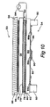
- FIG. 1 is an exploded perspective view illustrating the construction of a conventional membrane switch that includes an electroluminescent lamp
- FIG. 2 is a cross-sectional view of the present electroluminescent lamp membrane switch
- FIG. 3 is a cross-sectional view of an additional embodiment
- FIG. 4 is a cross-sectional view of an additional embodiment
- FIG. 5 is a cross-sectional view of an additional embodiment
- FIG. 6 is a cross-sectional view of an additional embodiment
- FIG. 7 is a cross-sectional view of an additional embodiment
- FIG. 8 is a cross-sectional view of an embodiment illustrating the construction of an electroluminescent lamp and portions of a membrane switch
- FIG. 9 is a cross-sectional view of an embodiment illustrating the construction of an electroluminescent lamp and portions of a membrane switch
- FIG. 10 is a cross-sectional view of an embodiment illustrating the construction of an electroluminescent lamp and portions of a membrane switch
- FIG. 11 is a cross-sectional view of an embodiment illustrating the construction of an electroluminescent lamp and portions of a membrane switch
- FIG. 12 is a cross-sectional view of an embodiment illustrating the construction of an electroluminescent lamp and portions of a membrane switch
- FIG. 13 is a cross-sectional view of preferred embodiment illustrating the construction of a monolithic electroluminescent lamp and membrane switch
- FIG. 14 is an illustration of a graphic display used with the disclosed embodiments.
- Switch 50 includes an electroluminescent lamp membrane system, generally identified by the numeral 52 , a membrane switch, generally identified by the numeral 54 and a graphics layer 56 .
- Lamp system 52 includes a top insulating layer 58 and a bottom insulating layer 60 .
- Top layer 58 has a front surface 58 a and a back surface 58 b .
- Bottom insulating layer 60 includes a front surface 60 a and a back surface 60 b .
- Lamp 62 includes various layers which will subsequently be described with respect to FIG. 8 .
- Lamp 62 may comprise, for example, the electroluminescent lamp shown and described in U.S. Pat. No. 5,856,030, which disclosure and drawings are hereby incorporated by reference.
- Top insulating layer 58 of lamp system 52 is directly imprinted on graphics layer 56 .
- Graphics layer 56 may include, for example, alpha numeric indicia which may be printed using a wide variety of inks, such as, for example, UV-cured polyurethane inks. No die cutting or lamination is required to form the combined graphics layer 56 and insulating layer 58 of lamp system 52 .
- Insulating layers 58 and 60 may comprise, for example, UV-curable polyurethane ink, inks cured by other means.
- Membrane switch 54 may be constructed in a continuous printing process, as described above, so that no layers need to be cut out or receive manual handling, thus creating a monolithic switch fabricated as a single structure.
- a layer 120 is printed into the switch between first and second conductive layers or traces 86 a , 90 for sensing actuation of the switch 54 .
- the layer for sensing actuation 120 may be a sensor for a change in capacitance (such as created by a user's finger approaching the switch), or a change in resistance due to pressure imparted by a user, or by detection of a magnetic field, such as that of a magnetic stylus.
- An illustration of the preferred embodiment is depicted in FIG. 13 .
- the layer for sensing actuation 120 of the monolithic membrane switch may be a curable polymer such as a urethane, epoxy, unsaturated and saturated acrylics and silicones in base resin compounds.
- the polymer to print the layer for sensing actuation 120 would then include, for example, carbon-impregnated powdered rubber, indium, indium-tin oxide, carbon powder, nano-carbon powder, or nano-silver powder for resistance-change sensing; silver-coated coppers, coated iron particles, or low-carbon steel particles for magnetic sensing; and ferro-electric compounds such as barium titanate for capacitance-change sensing, and in all cases, the equivalents thereof.
- switch 50 is illustrated as being integrally formed on a deformable substrate 66 which may comprise, for example, a layer of polycarbonate or polyester.
- Graphics layer 56 is directly printed on substrate 66 and is followed by insulating layer 58 .
- Substrate 66 provides a surface for a user to actuate switch 54 by depressing a portion of the deformable substrate 66 .
- Graphics layer 56 is protected by deformable substrate 66 since graphics layer 56 is disposed between deformable substrate 66 and insulating layer 58 .
- graphics layer 68 may be imprinted on the outer surface of deformable substrate 66 .
- Multiple layers of graphics may be included in switch 50 , as illustrated in FIG. 5 , wherein both graphic layers 56 and 68 are used and are imprinted on the inner and outer surfaces of deformable substrate 66 .
- multiple graphic indicia may be used with switch 50 and illuminated utilizing lamp system 52 .
- graphic layers 56 and 68 may include various indicia, and may further include various multicolored graphic designs.
- FIG. 6 further illustrates an additional embodiment of switch 50 in which insulating layer 58 is eliminated and lamp 62 is directly imprinted on deformable substrate 66 .
- FIG. 7 illustrates a further embodiment of switch 50 in which deformable substrate 66 is disposed between lamp system 52 and membrane switch 54 .
- Lamp 62 includes a bus bar 74 that is printed on insulating layer 58 .
- a transparent electrically conductive front electrode 76 is then printed onto insulating layer 58 .
- a phosphor layer 78 is printed and is disposed on front electrode 76 .
- a high dielectric constant layer 80 is then printed onto layer 78 .
- Layer 80 may contain, among other compositions, for example, barium titanate.
- a rear electrode 82 is imprinted on layer 80 .
- Electrode 82 may include electrically conductive ink, typically containing silver or graphite. The inks used to print the various layers of lamp 62 may include UV curable inks.
- Insulating layer 60 is printed onto electrode 82 to complete the lamp system 52 . Power is supplied to electrodes 74 and 82 from a power supply 84 .
- FIG. 8 also illustrates a component of membrane switch 54 including conductive pads 86 which are imprinted on insulating layer 60 .
- FIGS. 9-13 further illustrate components within membrane switch 54 .
- FIG. 9 illustrates an insulating layer 88 disposed on insulating layer 60 and between a conductive layer (typically a trace) 86 a which is part of an electrical switch circuit.
- An additional conductive layer (typically a pad) 90 is illustrated and is the other half of the switch circuit and is disposed opposite trace 86 a .
- FIG. 10 illustrates the further use of spacer elements 92 within switch 54 . (Note that spacer elements 92 are not required in monolithic switches printed by a continuous process).
- a snap dome 94 which provides tactile feedback to the user of the switch 50 .
- FIG. 12 illustrates the addition of adhesive layers 96 to spacers 92 .
- Adhesive layers 96 function to attach the remaining outer layer 100 ( FIG. 13 ) of switch 54 . (Note that the monolithic embodiment of the membrane switch 54 does not have an adhesive layer, since no separately-manufactured layers are assembled to create it.)
- FIG. 13 illustrates a completed monolithic switch 54 and electroluminescent lamp 62 , according to the preferred embodiment.
- Closure of switch 54 is accomplished by a user 102 applying pressure from the deformable substrate 66 , which, in the case of a layer for sensing actuation 120 of the switch comprising a resistance change, caused actuation of the switch by a conventional sensing circuit (not shown).
- the layer for sensing actuation 120 comprises material for sensing a change in capacitance, or a change in a magnetic field, as discussed above.
- FIG. 13 shows the layer for sensing actuation 120 as having optionally areas of particular sensitivity 125 for separate switching circuits within the same monolithic switch 54 .
- FIG. 14 illustrates an example of graphic indicia which may be included in graphics layers 56 , 68 and 62 .
- a display 104 includes a numeric display 106 and an alpha display 108 .
- Display 104 also includes the necessary electronic circuitry for illuminating segments within display 106 and 108 .
- Display 104 also includes an indicator light 110 .
Abstract
Description
Claims (12)
Priority Applications (6)
| Application Number | Priority Date | Filing Date | Title |
|---|---|---|---|
| US11/452,441 US8110765B2 (en) | 2005-06-09 | 2006-06-14 | Electroluminescent lamp membrane switch |
| CN2007800267152A CN101490776B (en) | 2006-06-14 | 2007-06-07 | Electroluminescent lamp membrane switch |
| PCT/US2007/013404 WO2008010879A2 (en) | 2006-06-14 | 2007-06-07 | Electroluminescent lamp membrane switch |
| EP20070835790 EP2038904A4 (en) | 2006-06-14 | 2007-06-07 | Electroluminescent lamp membrane switch |
| TW096121099A TWI396217B (en) | 2006-06-14 | 2007-06-12 | Electroluminescent lamp membrane switch |
| HK09112351.9A HK1132371A1 (en) | 2006-06-14 | 2009-12-31 | Electroluminescent lamp membrane switch |
Applications Claiming Priority (3)
| Application Number | Priority Date | Filing Date | Title |
|---|---|---|---|
| US11/148,216 US7049536B1 (en) | 2005-06-09 | 2005-06-09 | Electroluminescent lamp membrane switch |
| US11/438,182 US7186936B2 (en) | 2005-06-09 | 2006-05-22 | Electroluminescent lamp membrane switch |
| US11/452,441 US8110765B2 (en) | 2005-06-09 | 2006-06-14 | Electroluminescent lamp membrane switch |
Related Parent Applications (1)
| Application Number | Title | Priority Date | Filing Date |
|---|---|---|---|
| US11/438,182 Continuation-In-Part US7186936B2 (en) | 2005-06-09 | 2006-05-22 | Electroluminescent lamp membrane switch |
Publications (2)
| Publication Number | Publication Date |
|---|---|
| US20060278509A1 US20060278509A1 (en) | 2006-12-14 |
| US8110765B2 true US8110765B2 (en) | 2012-02-07 |
Family
ID=38957250
Family Applications (1)
| Application Number | Title | Priority Date | Filing Date |
|---|---|---|---|
| US11/452,441 Expired - Fee Related US8110765B2 (en) | 2005-06-09 | 2006-06-14 | Electroluminescent lamp membrane switch |
Country Status (6)
| Country | Link |
|---|---|
| US (1) | US8110765B2 (en) |
| EP (1) | EP2038904A4 (en) |
| CN (1) | CN101490776B (en) |
| HK (1) | HK1132371A1 (en) |
| TW (1) | TWI396217B (en) |
| WO (1) | WO2008010879A2 (en) |
Cited By (6)
| Publication number | Priority date | Publication date | Assignee | Title |
|---|---|---|---|---|
| US20110017580A1 (en) * | 2008-06-26 | 2011-01-27 | Nippon Mektron, Ltd. | Key module for mobile device |
| US20110209976A1 (en) * | 2010-03-01 | 2011-09-01 | Visteon Global Technologies, Inc. | Method for implementing capacitive sensing in the presence of conductive decorative materials |
| US20120247936A1 (en) * | 2011-04-01 | 2012-10-04 | Primax Electronics Ltd. | Illuminated keyboard |
| US20150242057A1 (en) * | 2014-02-27 | 2015-08-27 | Samsung Display Co., Ltd. | Technique for generating localized light source for an embedded optical sensor array |
| US10203797B2 (en) * | 2016-01-28 | 2019-02-12 | Boe Technology Group Co., Ltd. | Force touch structure, touch display panel, display apparatus |
| US10989399B2 (en) * | 2018-12-31 | 2021-04-27 | Lg Display Co., Ltd. | Electroluminescent lighting device having touch sensor |
Families Citing this family (9)
| Publication number | Priority date | Publication date | Assignee | Title |
|---|---|---|---|---|
| US20080094825A1 (en) * | 2006-10-18 | 2008-04-24 | Silver Norman L | Electroluminescent Candle |
| US7642479B2 (en) * | 2007-11-01 | 2010-01-05 | Sentalic Corporation | Touch pad structure |
| US8339040B2 (en) | 2007-12-18 | 2012-12-25 | Lumimove, Inc. | Flexible electroluminescent devices and systems |
| US8159370B2 (en) * | 2008-11-17 | 2012-04-17 | Canyon Ridge Resources, Llc | System and method for control of medical equipment using multiple wireless devices |
| US8274376B2 (en) * | 2008-11-17 | 2012-09-25 | Canyon Ridge Resources, L.L.C. | System and method for wireless control of medical devices |
| US8937561B2 (en) | 2008-11-17 | 2015-01-20 | Canyon Ridge Resources, L.L.C. | System and method for control of medical equipment using multiple wireless devices |
| GB0922165D0 (en) * | 2009-12-18 | 2010-02-03 | Pelikon Ltd | Human interface device and related methods |
| CN102737893B (en) * | 2011-04-08 | 2015-07-01 | 致伸科技股份有限公司 | Luminescent keyboard |
| CN104796128B (en) * | 2015-04-09 | 2018-01-12 | 昆山峰实电子科技有限公司 | A kind of electronic light decorations building materials and its production method |
Citations (75)
| Publication number | Priority date | Publication date | Assignee | Title |
|---|---|---|---|---|
| US3875449A (en) | 1969-10-02 | 1975-04-01 | U S Radium Corp | Coated phosphors |
| US4060703A (en) | 1976-11-10 | 1977-11-29 | Everett Jr Seth Leroy | Keyboard switch assembly with tactile feedback having illuminated laminated layers including opaque or transparent conductive layer |
| US4104555A (en) | 1977-01-27 | 1978-08-01 | Atkins & Merrill, Inc. | High temperature encapsulated electroluminescent lamp |
| US4261042A (en) * | 1978-03-28 | 1981-04-07 | Canon Kabushiki Kaisha | Key signal entering device for thin electronic apparatus |
| US4295699A (en) * | 1969-09-15 | 1981-10-20 | Essex International, Inc. | Pressure sensitive combination switch and circuit breaker construction |
| US4296406A (en) * | 1979-12-28 | 1981-10-20 | Sperry Corporation | Pressure sensitive switch structure |
| US4320268A (en) | 1980-02-19 | 1982-03-16 | General Electric Company | Illuminated keyboard for electronic devices and the like |
| US4532395A (en) | 1983-09-20 | 1985-07-30 | Timex Corporation | Electroluminescent flexible touch switch panel |
| US4548646A (en) | 1982-11-15 | 1985-10-22 | Sermatech International Incorporated | Thixotropic coating compositions and methods |
| US4647337A (en) | 1984-12-03 | 1987-03-03 | Luminescent Electronics, Inc. | Method of making electroluminescent panels |
| US4683360A (en) | 1986-05-09 | 1987-07-28 | W. H. Brady Co. | Membrane switch combined with electroluminescent lamp panel |
| US4684353A (en) | 1985-08-19 | 1987-08-04 | Dunmore Corporation | Flexible electroluminescent film laminate |
| US4743895A (en) | 1984-04-05 | 1988-05-10 | Phosphor Products Co. Ltd. | Capacitive switches |
| US4816717A (en) | 1984-02-06 | 1989-03-28 | Rogers Corporation | Electroluminescent lamp having a polymer phosphor layer formed in substantially a non-crossed linked state |
| US4853079A (en) | 1984-12-03 | 1989-08-01 | Lumel, Inc. | Method for making electroluminescent panels |
| US4853594A (en) | 1988-08-10 | 1989-08-01 | Rogers Corporation | Electroluminescent lamp |
| US4999936A (en) | 1988-04-24 | 1991-03-19 | Calamia Thomas J | Illuminated sign |
| US5041326A (en) | 1975-04-11 | 1991-08-20 | Schroeder Becky J | Electroluminescent laminate assembly |
| US5184969A (en) | 1988-05-31 | 1993-02-09 | Electroluminscent Technologies Corporation | Electroluminescent lamp and method for producing the same |
| US5243060A (en) | 1992-04-10 | 1993-09-07 | Iowa State University Research Foundation, Inc. | Silylene-diethynyl-arylene polymers having liquid crystalline properties |
| US5317488A (en) | 1992-11-17 | 1994-05-31 | Darlene Penrod | Insulated integral electroluminescent lighting system |
| US5336345A (en) | 1991-03-13 | 1994-08-09 | The Standard Products Company | Process for manufacturing an elongated electroluminescent light strip |
| US5434757A (en) * | 1992-04-01 | 1995-07-18 | Kasai Kogyo Co., Ltd. | Unit panel structure for a door trim |
| US5475574A (en) | 1994-04-12 | 1995-12-12 | Chien; Tseng-Lu | Shoulder band with an EL light strip |
| US5491377A (en) | 1993-08-03 | 1996-02-13 | Janusauskas; Albert | Electroluminescent lamp and method |
| US5496427A (en) | 1991-03-13 | 1996-03-05 | The Standard Products Company | Process for manufacturing an elongated electroluminescent light strip |
| US5559680A (en) | 1995-04-11 | 1996-09-24 | Tabanera; Dennis A. | Electroluminescent bicycle helmet |
| US5565733A (en) | 1992-12-16 | 1996-10-15 | Durel Corporation | Electroluminescent modular lamp unit |
| US5567040A (en) | 1995-04-11 | 1996-10-22 | Tabanera; Dennis A. | Electroluminescent jacket and bag |
| US5569893A (en) | 1995-04-10 | 1996-10-29 | Takata Inc. | Driver air bag cover with integral horn and redundant switches |
| US5570945A (en) | 1993-11-22 | 1996-11-05 | Chien; Tseng-Lu | Soft light-strip |
| US5597183A (en) | 1994-12-06 | 1997-01-28 | Junkyard Dogs, Ltd. | Interactive book having electroluminescent display pages and animation effects |
| US5611621A (en) | 1994-04-12 | 1997-03-18 | Chien; Tseng-Lu | Shoe with an EL light strip |
| US5680160A (en) | 1995-02-09 | 1997-10-21 | Leading Edge Industries, Inc. | Touch activated electroluminescent lamp and display switch |
| US5688038A (en) | 1995-04-13 | 1997-11-18 | Chien; Tseng Lu | Protective device with E.L. light means |
| US5701189A (en) | 1995-03-27 | 1997-12-23 | Motorola, Inc. | Wireless data communication system and method using an electroluminescent panel |
| US5726953A (en) | 1995-04-07 | 1998-03-10 | Metro-Mark, Incorporated | Electroluminescent lamp with buried indiciae and method for making same |
| US5747756A (en) | 1996-09-10 | 1998-05-05 | Gm Nameplate, Inc. | Electroluminescent backlit keypad |
| US5746501A (en) | 1995-09-01 | 1998-05-05 | Chien; Tseng Lu | Portable object having a fastening band illuminated by a super thin lighting element |
| US5770920A (en) | 1995-06-06 | 1998-06-23 | Durel Corporation | Electroluminescent lamp having a terpolymer binder |
| US5772924A (en) | 1994-06-14 | 1998-06-30 | Mitsui Mining & Smelting Co., Ltd. | Composite conductive powder and conductive film formed from the powder |
| US5794366A (en) | 1994-09-15 | 1998-08-18 | Chien; Tseng-Lu | Multiple segment electro-luminescent lighting arrangement |
| US5797482A (en) | 1996-11-25 | 1998-08-25 | Metro-Mark, Inc. | Electroluminescent keypad |
| US5806960A (en) | 1996-11-08 | 1998-09-15 | Chien; Tseng Lu | Universal safety light with EL element |
| US5810467A (en) | 1995-04-07 | 1998-09-22 | Hurwitz; Marni M. | Electroluminescent illuminated protective hat such as a hard hat, helmet and the like, and a retrofit unit for retrofitting existing protective hats to include an electroluminescent illumination device |
| US5818174A (en) | 1996-03-01 | 1998-10-06 | Matsushita Electric Industrial Co., Ltd. | Noiseless dispersion electroluminescent device and switch unit using same |
| US5836671A (en) | 1994-11-17 | 1998-11-17 | Chien; Tseng Lu | Backpack or waistpack E.L. lighting arrangement |
| US5856029A (en) | 1996-05-30 | 1999-01-05 | E.L. Specialists, Inc. | Electroluminescent system in monolithic structure |
| US5856030A (en) | 1996-12-30 | 1999-01-05 | E.L. Specialists, Inc. | Elastomeric electroluminescent lamp |
| US5856031A (en) | 1996-05-30 | 1999-01-05 | E.L. Specialists, Inc. | EL lamp system in kit form |
| US5860727A (en) | 1994-04-12 | 1999-01-19 | Chien; Tseng-Lu | Shoe with an electro-luminescent lighting element |
| US5865523A (en) | 1994-04-12 | 1999-02-02 | Chien; Tseng-Lu | Shoe with an EL light strip |
| US5871271A (en) | 1995-11-30 | 1999-02-16 | Chien; Tseng Lu | LED illuminated protective headwear |
| US5871088A (en) | 1995-03-30 | 1999-02-16 | Matsushita Electric Industrial Co.,Ltd. | EL sheet diaphragm and a switch using the same |
| US5879069A (en) | 1996-03-05 | 1999-03-09 | Chien; Tseng Lu | EL light strip device for footwear |
| US5917437A (en) * | 1994-12-28 | 1999-06-29 | Screentec Ky | Keyboard |
| US5921653A (en) | 1995-05-02 | 1999-07-13 | Chien; Tseng-Lu | Super-thin lighting arrangement for a moving object |
| US6144157A (en) | 1998-05-18 | 2000-11-07 | Motorola, Inc. | Organic EL device with fluorocarbon liquid and UV epoxy layers and method |
| US6198217B1 (en) | 1997-05-12 | 2001-03-06 | Matsushita Electric Industrial Co., Ltd. | Organic electroluminescent device having a protective covering comprising organic and inorganic layers |
| US6261633B1 (en) | 1996-05-30 | 2001-07-17 | E.L. Specialists, Inc. | Translucent layer including metal/metal oxide dopant suspended in gel resin |
| US6271631B1 (en) | 1998-10-15 | 2001-08-07 | E.L. Specialists, Inc. | Alerting system using elastomeric EL lamp structure |
| US6310614B1 (en) * | 1998-07-15 | 2001-10-30 | Smk Corporation | Touch-panel input device |
| US20010037933A1 (en) | 1999-06-17 | 2001-11-08 | Hunter Richard Stuart | Illuminated membrane switch |
| US6373008B1 (en) | 1999-03-12 | 2002-04-16 | Seiko Precision, Inc. | Light illuminating type switch |
| US6379743B1 (en) | 1997-10-10 | 2002-04-30 | Nessdisplay, Co. Ltd. | Process for the preparation of organic electroluminescent device using vapor deposition polymerization |
| US6512250B1 (en) | 1999-06-10 | 2003-01-28 | Seiko Epson Corporation | Light-emitting device |
| US20030041443A1 (en) | 2001-08-30 | 2003-03-06 | Novatech Electroluminescent, Inc. | Method for manufacturing low cost electroluminescent (EL) illuminated membrane switches |
| US6717361B2 (en) | 2000-10-11 | 2004-04-06 | Mrm Acquisitions, Llc | Membranous EL system in UV-cured urethane envelope |
| US6809280B2 (en) * | 2002-05-02 | 2004-10-26 | 3M Innovative Properties Company | Pressure activated switch and touch panel |
| US6824288B2 (en) | 2000-06-08 | 2004-11-30 | Rick D. Prindle | Method and apparatus for illuminating a keypad |
| US6875938B2 (en) | 2000-06-09 | 2005-04-05 | I.E.E. International Electronics & Engineering S.Ar.L. | Illuminated switch element |
| US7106222B2 (en) * | 2002-09-19 | 2006-09-12 | Siemens Communications, Inc. | Keypad assembly |
| US7158276B1 (en) * | 2006-03-24 | 2007-01-02 | Daxon Technology Inc. | Pressure sensitive electrochromic device and method of fabricating the same |
| US7230198B2 (en) * | 2004-11-12 | 2007-06-12 | Eastman Kodak Company | Flexible sheet for resistive touch screen |
| US7468199B2 (en) * | 2004-12-23 | 2008-12-23 | 3M Innovative Properties Company | Adhesive membrane for force switches and sensors |
Family Cites Families (5)
| Publication number | Priority date | Publication date | Assignee | Title |
|---|---|---|---|---|
| US5072077A (en) * | 1991-02-21 | 1991-12-10 | Harold Klein | Monolithic membrane switch |
| ES2084235T3 (en) * | 1991-11-22 | 1996-05-01 | Marquardt Gmbh | ELECTRIC SWITCH. |
| JP2001228975A (en) * | 2000-02-16 | 2001-08-24 | Fujikura Ltd | Pressure sensitive element, touch panel and liquid crystal display using the same |
| US6782166B1 (en) * | 2001-12-21 | 2004-08-24 | United States Of America As Represented By The Secretary Of The Air Force | Optically transparent electrically conductive charge sheet poling electrodes to maximize performance of electro-optic devices |
| US7049536B1 (en) * | 2005-06-09 | 2006-05-23 | Oryon Technologies, Llc | Electroluminescent lamp membrane switch |
-
2006
- 2006-06-14 US US11/452,441 patent/US8110765B2/en not_active Expired - Fee Related
-
2007
- 2007-06-07 EP EP20070835790 patent/EP2038904A4/en not_active Withdrawn
- 2007-06-07 WO PCT/US2007/013404 patent/WO2008010879A2/en active Application Filing
- 2007-06-07 CN CN2007800267152A patent/CN101490776B/en not_active Expired - Fee Related
- 2007-06-12 TW TW096121099A patent/TWI396217B/en not_active IP Right Cessation
-
2009
- 2009-12-31 HK HK09112351.9A patent/HK1132371A1/en not_active IP Right Cessation
Patent Citations (84)
| Publication number | Priority date | Publication date | Assignee | Title |
|---|---|---|---|---|
| US4295699A (en) * | 1969-09-15 | 1981-10-20 | Essex International, Inc. | Pressure sensitive combination switch and circuit breaker construction |
| US3875449A (en) | 1969-10-02 | 1975-04-01 | U S Radium Corp | Coated phosphors |
| US5041326A (en) | 1975-04-11 | 1991-08-20 | Schroeder Becky J | Electroluminescent laminate assembly |
| US4060703A (en) | 1976-11-10 | 1977-11-29 | Everett Jr Seth Leroy | Keyboard switch assembly with tactile feedback having illuminated laminated layers including opaque or transparent conductive layer |
| US4104555A (en) | 1977-01-27 | 1978-08-01 | Atkins & Merrill, Inc. | High temperature encapsulated electroluminescent lamp |
| US4261042A (en) * | 1978-03-28 | 1981-04-07 | Canon Kabushiki Kaisha | Key signal entering device for thin electronic apparatus |
| US4296406A (en) * | 1979-12-28 | 1981-10-20 | Sperry Corporation | Pressure sensitive switch structure |
| US4320268A (en) | 1980-02-19 | 1982-03-16 | General Electric Company | Illuminated keyboard for electronic devices and the like |
| US4548646A (en) | 1982-11-15 | 1985-10-22 | Sermatech International Incorporated | Thixotropic coating compositions and methods |
| US4532395A (en) | 1983-09-20 | 1985-07-30 | Timex Corporation | Electroluminescent flexible touch switch panel |
| US4816717A (en) | 1984-02-06 | 1989-03-28 | Rogers Corporation | Electroluminescent lamp having a polymer phosphor layer formed in substantially a non-crossed linked state |
| US4743895A (en) | 1984-04-05 | 1988-05-10 | Phosphor Products Co. Ltd. | Capacitive switches |
| US4647337A (en) | 1984-12-03 | 1987-03-03 | Luminescent Electronics, Inc. | Method of making electroluminescent panels |
| US4853079A (en) | 1984-12-03 | 1989-08-01 | Lumel, Inc. | Method for making electroluminescent panels |
| US4684353A (en) | 1985-08-19 | 1987-08-04 | Dunmore Corporation | Flexible electroluminescent film laminate |
| US4683360A (en) | 1986-05-09 | 1987-07-28 | W. H. Brady Co. | Membrane switch combined with electroluminescent lamp panel |
| US4999936A (en) | 1988-04-24 | 1991-03-19 | Calamia Thomas J | Illuminated sign |
| US5184969A (en) | 1988-05-31 | 1993-02-09 | Electroluminscent Technologies Corporation | Electroluminescent lamp and method for producing the same |
| US4853594A (en) | 1988-08-10 | 1989-08-01 | Rogers Corporation | Electroluminescent lamp |
| US5496427A (en) | 1991-03-13 | 1996-03-05 | The Standard Products Company | Process for manufacturing an elongated electroluminescent light strip |
| US5336345A (en) | 1991-03-13 | 1994-08-09 | The Standard Products Company | Process for manufacturing an elongated electroluminescent light strip |
| US5434757A (en) * | 1992-04-01 | 1995-07-18 | Kasai Kogyo Co., Ltd. | Unit panel structure for a door trim |
| US5243060A (en) | 1992-04-10 | 1993-09-07 | Iowa State University Research Foundation, Inc. | Silylene-diethynyl-arylene polymers having liquid crystalline properties |
| US5317488A (en) | 1992-11-17 | 1994-05-31 | Darlene Penrod | Insulated integral electroluminescent lighting system |
| US5811930A (en) | 1992-12-16 | 1998-09-22 | Durel Corporation | Electroluminescent lamp devices and their manufacture |
| US5565733A (en) | 1992-12-16 | 1996-10-15 | Durel Corporation | Electroluminescent modular lamp unit |
| US5491377A (en) | 1993-08-03 | 1996-02-13 | Janusauskas; Albert | Electroluminescent lamp and method |
| US5570945A (en) | 1993-11-22 | 1996-11-05 | Chien; Tseng-Lu | Soft light-strip |
| US5475574A (en) | 1994-04-12 | 1995-12-12 | Chien; Tseng-Lu | Shoulder band with an EL light strip |
| US5860727A (en) | 1994-04-12 | 1999-01-19 | Chien; Tseng-Lu | Shoe with an electro-luminescent lighting element |
| US5865523A (en) | 1994-04-12 | 1999-02-02 | Chien; Tseng-Lu | Shoe with an EL light strip |
| US5704705A (en) | 1994-04-12 | 1998-01-06 | Chien; Tseng-Lu | Shoe with an EL light strip |
| US5611621A (en) | 1994-04-12 | 1997-03-18 | Chien; Tseng-Lu | Shoe with an EL light strip |
| US5772924A (en) | 1994-06-14 | 1998-06-30 | Mitsui Mining & Smelting Co., Ltd. | Composite conductive powder and conductive film formed from the powder |
| US5794366A (en) | 1994-09-15 | 1998-08-18 | Chien; Tseng-Lu | Multiple segment electro-luminescent lighting arrangement |
| US5836671A (en) | 1994-11-17 | 1998-11-17 | Chien; Tseng Lu | Backpack or waistpack E.L. lighting arrangement |
| US5597183A (en) | 1994-12-06 | 1997-01-28 | Junkyard Dogs, Ltd. | Interactive book having electroluminescent display pages and animation effects |
| US5917437A (en) * | 1994-12-28 | 1999-06-29 | Screentec Ky | Keyboard |
| US5680160A (en) | 1995-02-09 | 1997-10-21 | Leading Edge Industries, Inc. | Touch activated electroluminescent lamp and display switch |
| US5701189A (en) | 1995-03-27 | 1997-12-23 | Motorola, Inc. | Wireless data communication system and method using an electroluminescent panel |
| US5871088A (en) | 1995-03-30 | 1999-02-16 | Matsushita Electric Industrial Co.,Ltd. | EL sheet diaphragm and a switch using the same |
| US5810467A (en) | 1995-04-07 | 1998-09-22 | Hurwitz; Marni M. | Electroluminescent illuminated protective hat such as a hard hat, helmet and the like, and a retrofit unit for retrofitting existing protective hats to include an electroluminescent illumination device |
| US5726953A (en) | 1995-04-07 | 1998-03-10 | Metro-Mark, Incorporated | Electroluminescent lamp with buried indiciae and method for making same |
| US5569893A (en) | 1995-04-10 | 1996-10-29 | Takata Inc. | Driver air bag cover with integral horn and redundant switches |
| US5567040A (en) | 1995-04-11 | 1996-10-22 | Tabanera; Dennis A. | Electroluminescent jacket and bag |
| US5559680A (en) | 1995-04-11 | 1996-09-24 | Tabanera; Dennis A. | Electroluminescent bicycle helmet |
| US5688038A (en) | 1995-04-13 | 1997-11-18 | Chien; Tseng Lu | Protective device with E.L. light means |
| US5921653A (en) | 1995-05-02 | 1999-07-13 | Chien; Tseng-Lu | Super-thin lighting arrangement for a moving object |
| US5770920A (en) | 1995-06-06 | 1998-06-23 | Durel Corporation | Electroluminescent lamp having a terpolymer binder |
| US5746501A (en) | 1995-09-01 | 1998-05-05 | Chien; Tseng Lu | Portable object having a fastening band illuminated by a super thin lighting element |
| US5871271A (en) | 1995-11-30 | 1999-02-16 | Chien; Tseng Lu | LED illuminated protective headwear |
| US5818174A (en) | 1996-03-01 | 1998-10-06 | Matsushita Electric Industrial Co., Ltd. | Noiseless dispersion electroluminescent device and switch unit using same |
| US5879069A (en) | 1996-03-05 | 1999-03-09 | Chien; Tseng Lu | EL light strip device for footwear |
| US5856031A (en) | 1996-05-30 | 1999-01-05 | E.L. Specialists, Inc. | EL lamp system in kit form |
| US5856029A (en) | 1996-05-30 | 1999-01-05 | E.L. Specialists, Inc. | Electroluminescent system in monolithic structure |
| US5980976A (en) | 1996-05-30 | 1999-11-09 | E.L. Specialists, Inc. | Method for constructing el system in monolithic structure |
| US6261633B1 (en) | 1996-05-30 | 2001-07-17 | E.L. Specialists, Inc. | Translucent layer including metal/metal oxide dopant suspended in gel resin |
| US5747756A (en) | 1996-09-10 | 1998-05-05 | Gm Nameplate, Inc. | Electroluminescent backlit keypad |
| US5947580A (en) | 1996-11-08 | 1999-09-07 | Chien; Tseng Lu | Universal safety light with EL element |
| US5806960A (en) | 1996-11-08 | 1998-09-15 | Chien; Tseng Lu | Universal safety light with EL element |
| US6100478A (en) | 1996-11-25 | 2000-08-08 | Metro-Mark Incorporated | Electroluminescent keypad |
| US5797482A (en) | 1996-11-25 | 1998-08-25 | Metro-Mark, Inc. | Electroluminescent keypad |
| US6309764B1 (en) | 1996-12-30 | 2001-10-30 | E.L. Specialists, Inc. | Elastomeric EL lamp on apparel |
| US5856030A (en) | 1996-12-30 | 1999-01-05 | E.L. Specialists, Inc. | Elastomeric electroluminescent lamp |
| US6270834B1 (en) | 1996-12-30 | 2001-08-07 | E.L. Specialists, Inc. | Method for construction of elastomeric EL lamp |
| US6198217B1 (en) | 1997-05-12 | 2001-03-06 | Matsushita Electric Industrial Co., Ltd. | Organic electroluminescent device having a protective covering comprising organic and inorganic layers |
| US6379743B1 (en) | 1997-10-10 | 2002-04-30 | Nessdisplay, Co. Ltd. | Process for the preparation of organic electroluminescent device using vapor deposition polymerization |
| US6144157A (en) | 1998-05-18 | 2000-11-07 | Motorola, Inc. | Organic EL device with fluorocarbon liquid and UV epoxy layers and method |
| US6310614B1 (en) * | 1998-07-15 | 2001-10-30 | Smk Corporation | Touch-panel input device |
| US20040069607A1 (en) | 1998-08-20 | 2004-04-15 | Screen Sign Arts, Ltd. | Illuminated membrane switch |
| US6271631B1 (en) | 1998-10-15 | 2001-08-07 | E.L. Specialists, Inc. | Alerting system using elastomeric EL lamp structure |
| US6373008B1 (en) | 1999-03-12 | 2002-04-16 | Seiko Precision, Inc. | Light illuminating type switch |
| US6512250B1 (en) | 1999-06-10 | 2003-01-28 | Seiko Epson Corporation | Light-emitting device |
| US20010037933A1 (en) | 1999-06-17 | 2001-11-08 | Hunter Richard Stuart | Illuminated membrane switch |
| US6824288B2 (en) | 2000-06-08 | 2004-11-30 | Rick D. Prindle | Method and apparatus for illuminating a keypad |
| US6875938B2 (en) | 2000-06-09 | 2005-04-05 | I.E.E. International Electronics & Engineering S.Ar.L. | Illuminated switch element |
| US6717361B2 (en) | 2000-10-11 | 2004-04-06 | Mrm Acquisitions, Llc | Membranous EL system in UV-cured urethane envelope |
| US6698085B2 (en) | 2001-08-30 | 2004-03-02 | Novatech Electro-Luminescent, Inc. | Method for manufacturing low cost electroluminescent (EL) illuminated membrane switches |
| US20030041443A1 (en) | 2001-08-30 | 2003-03-06 | Novatech Electroluminescent, Inc. | Method for manufacturing low cost electroluminescent (EL) illuminated membrane switches |
| US6809280B2 (en) * | 2002-05-02 | 2004-10-26 | 3M Innovative Properties Company | Pressure activated switch and touch panel |
| US7106222B2 (en) * | 2002-09-19 | 2006-09-12 | Siemens Communications, Inc. | Keypad assembly |
| US7230198B2 (en) * | 2004-11-12 | 2007-06-12 | Eastman Kodak Company | Flexible sheet for resistive touch screen |
| US7468199B2 (en) * | 2004-12-23 | 2008-12-23 | 3M Innovative Properties Company | Adhesive membrane for force switches and sensors |
| US7158276B1 (en) * | 2006-03-24 | 2007-01-02 | Daxon Technology Inc. | Pressure sensitive electrochromic device and method of fabricating the same |
Non-Patent Citations (1)
| Title |
|---|
| International Searching Authority, International Application No. PCT/US2007/013404, International Search Report and the Written Opinion, Aug. 28, 2008. |
Cited By (9)
| Publication number | Priority date | Publication date | Assignee | Title |
|---|---|---|---|---|
| US20110017580A1 (en) * | 2008-06-26 | 2011-01-27 | Nippon Mektron, Ltd. | Key module for mobile device |
| US8367950B2 (en) * | 2008-06-26 | 2013-02-05 | Nippon Mektron, Ltd. | Key module for mobile device |
| US20110209976A1 (en) * | 2010-03-01 | 2011-09-01 | Visteon Global Technologies, Inc. | Method for implementing capacitive sensing in the presence of conductive decorative materials |
| US8629364B2 (en) * | 2010-03-01 | 2014-01-14 | Visteon Global Technologies, Inc. | Method for implementing capacitive sensing in the presence of conductive decorative materials |
| US20120247936A1 (en) * | 2011-04-01 | 2012-10-04 | Primax Electronics Ltd. | Illuminated keyboard |
| US8513549B2 (en) * | 2011-04-01 | 2013-08-20 | Primax Electronics, Ltd. | Illuminated keyboard |
| US20150242057A1 (en) * | 2014-02-27 | 2015-08-27 | Samsung Display Co., Ltd. | Technique for generating localized light source for an embedded optical sensor array |
| US10203797B2 (en) * | 2016-01-28 | 2019-02-12 | Boe Technology Group Co., Ltd. | Force touch structure, touch display panel, display apparatus |
| US10989399B2 (en) * | 2018-12-31 | 2021-04-27 | Lg Display Co., Ltd. | Electroluminescent lighting device having touch sensor |
Also Published As
| Publication number | Publication date |
|---|---|
| WO2008010879A2 (en) | 2008-01-24 |
| EP2038904A4 (en) | 2013-09-11 |
| TWI396217B (en) | 2013-05-11 |
| WO2008010879A3 (en) | 2008-11-06 |
| EP2038904A2 (en) | 2009-03-25 |
| TW200802456A (en) | 2008-01-01 |
| US20060278509A1 (en) | 2006-12-14 |
| HK1132371A1 (en) | 2010-02-19 |
| CN101490776A (en) | 2009-07-22 |
| CN101490776B (en) | 2012-08-29 |
Similar Documents
| Publication | Publication Date | Title |
|---|---|---|
| US8110765B2 (en) | Electroluminescent lamp membrane switch | |
| US7186936B2 (en) | Electroluminescent lamp membrane switch | |
| US6698085B2 (en) | Method for manufacturing low cost electroluminescent (EL) illuminated membrane switches | |
| EP0938737B1 (en) | Electroluminescent backlit devices | |
| US8441445B2 (en) | Electrophoretic display keypad structure | |
| KR100649647B1 (en) | EL metal dome sheet for backlight of keypad | |
| US7532131B2 (en) | Multi-layer solid state keyboard | |
| US20060291186A1 (en) | Electroluminescent lamp with graphical overlay | |
| WO2010001805A1 (en) | Protective panel with touch input function for electronic equipment display panel | |
| US10090122B2 (en) | Low profile keyboard backlight module | |
| KR20060116057A (en) | The metal dome switch one body type electroluminescence lamp and manufacturing method of the same | |
| JP2008288169A (en) | Member for keyswitch | |
| JP2010257986A (en) | Multi-layer solid state keyboard | |
| US7619358B2 (en) | Dispersion-type EL device and illuminated switch unit using the same | |
| KR100790560B1 (en) | A thin film keypad and method for manufacturing thereof | |
| JPH11149841A (en) | Information inputting key | |
| KR200406245Y1 (en) | EL sheet using Multi-Layer Thin Film and EL metal dome sheet using thereof | |
| KR100773713B1 (en) | El device and key pad using the same | |
| CN102117708A (en) | Electrophoretic display key structure | |
| KR100783562B1 (en) | El keypad and fabricating method of the same | |
| KR20040062775A (en) | Key pad and method for manufacturing the key pad |
Legal Events
| Date | Code | Title | Description |
|---|---|---|---|
| AS | Assignment |
Owner name: ORYONTECHNOLOGIES, LLC, TEXAS Free format text: ASSIGNMENT OF ASSIGNORS INTEREST;ASSIGNOR:BURROWS, KENNETH;REEL/FRAME:023357/0961 Effective date: 20091006 |
|
| ZAAA | Notice of allowance and fees due |
Free format text: ORIGINAL CODE: NOA |
|
| ZAAB | Notice of allowance mailed |
Free format text: ORIGINAL CODE: MN/=. |
|
| STCF | Information on status: patent grant |
Free format text: PATENTED CASE |
|
| AS | Assignment |
Owner name: MRM ACQUISITIONS, LLC, TEXAS Free format text: SECURITY INTEREST;ASSIGNORS:ORYON TECHNOLOGIES, LLC;ORYON TECHNOLOGIES, INC.;ORYON TECHNOLOGIES LICENSING, LLC;REEL/FRAME:034788/0870 Effective date: 20141120 Owner name: MYANT CAPITAL PARTNERS, INC., CANADA Free format text: SECURITY INTEREST;ASSIGNORS:ORYON TECHNOLOGIES, LLC;ORYON TECHNOLOGIES, INC.;ORYON TECHNOLOGIES LICENSING, LLC;REEL/FRAME:034788/0870 Effective date: 20141120 Owner name: ORYON CAPITAL, LLC, TEXAS Free format text: SECURITY INTEREST;ASSIGNORS:ORYON TECHNOLOGIES, LLC;ORYON TECHNOLOGIES, INC.;ORYON TECHNOLOGIES LICENSING, LLC;REEL/FRAME:034788/0870 Effective date: 20141120 Owner name: MARCUS, M. RICHARD, TEXAS Free format text: SECURITY INTEREST;ASSIGNORS:ORYON TECHNOLOGIES, LLC;ORYON TECHNOLOGIES, INC.;ORYON TECHNOLOGIES LICENSING, LLC;REEL/FRAME:034788/0870 Effective date: 20141120 |
|
| AS | Assignment |
Owner name: EL PATENT ACQUISITION, LLC, TEXAS Free format text: ASSIGNMENT OF ASSIGNORS INTEREST;ASSIGNORS:ORYONTECHNOLOGIES, LLC;ORYON TECHNOLOGIES, INC;ORYONTECHNOLOGIES LICENSING, LLC;REEL/FRAME:035352/0796 Effective date: 20150309 |
|
| AS | Assignment |
Owner name: 2461729 ONTARIO INC., CANADA Free format text: ASSIGNMENT OF ASSIGNORS INTEREST;ASSIGNOR:EL PATENT ACQUISITION LLC;REEL/FRAME:035886/0759 Effective date: 20150420 |
|
| FPAY | Fee payment |
Year of fee payment: 4 |
|
| FEPP | Fee payment procedure |
Free format text: 7.5 YR SURCHARGE - LATE PMT W/IN 6 MO, SMALL ENTITY (ORIGINAL EVENT CODE: M2555); ENTITY STATUS OF PATENT OWNER: SMALL ENTITY |
|
| MAFP | Maintenance fee payment |
Free format text: PAYMENT OF MAINTENANCE FEE, 8TH YR, SMALL ENTITY (ORIGINAL EVENT CODE: M2552); ENTITY STATUS OF PATENT OWNER: SMALL ENTITY Year of fee payment: 8 |
|
| FEPP | Fee payment procedure |
Free format text: MAINTENANCE FEE REMINDER MAILED (ORIGINAL EVENT CODE: REM.); ENTITY STATUS OF PATENT OWNER: SMALL ENTITY |
|
| LAPS | Lapse for failure to pay maintenance fees |
Free format text: PATENT EXPIRED FOR FAILURE TO PAY MAINTENANCE FEES (ORIGINAL EVENT CODE: EXP.); ENTITY STATUS OF PATENT OWNER: SMALL ENTITY |
|
| STCH | Information on status: patent discontinuation |
Free format text: PATENT EXPIRED DUE TO NONPAYMENT OF MAINTENANCE FEES UNDER 37 CFR 1.362 |
|
| FP | Lapsed due to failure to pay maintenance fee |
Effective date: 20240207 |