US8099865B2 - Method for manufacturing a circuit board having an embedded component therein - Google Patents

Method for manufacturing a circuit board having an embedded component therein Download PDF

Info

Publication number
US8099865B2
US8099865B2 US12/142,853 US14285308A US8099865B2 US 8099865 B2 US8099865 B2 US 8099865B2 US 14285308 A US14285308 A US 14285308A US 8099865 B2 US8099865 B2 US 8099865B2
Authority
US
United States
Prior art keywords
layer
embedded component
electrode
thickness
layers
Prior art date
Legal status (The legal status is an assumption and is not a legal conclusion. Google has not performed a legal analysis and makes no representation as to the accuracy of the status listed.)
Active, expires
Application number
US12/142,853
Other versions
US20090249618A1 (en
Inventor
Yung Hui Wang
Ying Te OU
Current Assignee (The listed assignees may be inaccurate. Google has not performed a legal analysis and makes no representation or warranty as to the accuracy of the list.)
Advanced Semiconductor Engineering Inc
Original Assignee
Advanced Semiconductor Engineering Inc
Priority date (The priority date is an assumption and is not a legal conclusion. Google has not performed a legal analysis and makes no representation as to the accuracy of the date listed.)
Filing date
Publication date
Application filed by Advanced Semiconductor Engineering Inc filed Critical Advanced Semiconductor Engineering Inc
Assigned to ADVANCED SEMICONDUCTOR ENGINEERING, INC. reassignment ADVANCED SEMICONDUCTOR ENGINEERING, INC. ASSIGNMENT OF ASSIGNORS INTEREST (SEE DOCUMENT FOR DETAILS). Assignors: OU, YING TE, WANG, YUNG HUI
Publication of US20090249618A1 publication Critical patent/US20090249618A1/en
Application granted granted Critical
Publication of US8099865B2 publication Critical patent/US8099865B2/en
Active legal-status Critical Current
Adjusted expiration legal-status Critical

Links

Images

Classifications

    • HELECTRICITY
    • H05ELECTRIC TECHNIQUES NOT OTHERWISE PROVIDED FOR
    • H05KPRINTED CIRCUITS; CASINGS OR CONSTRUCTIONAL DETAILS OF ELECTRIC APPARATUS; MANUFACTURE OF ASSEMBLAGES OF ELECTRICAL COMPONENTS
    • H05K1/00Printed circuits
    • H05K1/18Printed circuits structurally associated with non-printed electric components
    • H05K1/182Printed circuits structurally associated with non-printed electric components associated with components mounted in the printed circuit board, e.g. insert mounted components [IMC]
    • H05K1/185Components encapsulated in the insulating substrate of the printed circuit or incorporated in internal layers of a multilayer circuit
    • HELECTRICITY
    • H01ELECTRIC ELEMENTS
    • H01LSEMICONDUCTOR DEVICES NOT COVERED BY CLASS H10
    • H01L23/00Details of semiconductor or other solid state devices
    • H01L23/52Arrangements for conducting electric current within the device in operation from one component to another, i.e. interconnections, e.g. wires, lead frames
    • H01L23/538Arrangements for conducting electric current within the device in operation from one component to another, i.e. interconnections, e.g. wires, lead frames the interconnection structure between a plurality of semiconductor chips being formed on, or in, insulating substrates
    • H01L23/5389Arrangements for conducting electric current within the device in operation from one component to another, i.e. interconnections, e.g. wires, lead frames the interconnection structure between a plurality of semiconductor chips being formed on, or in, insulating substrates the chips being integrally enclosed by the interconnect and support structures
    • HELECTRICITY
    • H01ELECTRIC ELEMENTS
    • H01LSEMICONDUCTOR DEVICES NOT COVERED BY CLASS H10
    • H01L24/00Arrangements for connecting or disconnecting semiconductor or solid-state bodies; Methods or apparatus related thereto
    • H01L24/01Means for bonding being attached to, or being formed on, the surface to be connected, e.g. chip-to-package, die-attach, "first-level" interconnects; Manufacturing methods related thereto
    • H01L24/18High density interconnect [HDI] connectors; Manufacturing methods related thereto
    • H01L24/19Manufacturing methods of high density interconnect preforms
    • HELECTRICITY
    • H01ELECTRIC ELEMENTS
    • H01LSEMICONDUCTOR DEVICES NOT COVERED BY CLASS H10
    • H01L24/00Arrangements for connecting or disconnecting semiconductor or solid-state bodies; Methods or apparatus related thereto
    • H01L24/80Methods for connecting semiconductor or other solid state bodies using means for bonding being attached to, or being formed on, the surface to be connected
    • H01L24/82Methods for connecting semiconductor or other solid state bodies using means for bonding being attached to, or being formed on, the surface to be connected by forming build-up interconnects at chip-level, e.g. for high density interconnects [HDI]
    • HELECTRICITY
    • H01ELECTRIC ELEMENTS
    • H01LSEMICONDUCTOR DEVICES NOT COVERED BY CLASS H10
    • H01L24/00Arrangements for connecting or disconnecting semiconductor or solid-state bodies; Methods or apparatus related thereto
    • H01L24/93Batch processes
    • H01L24/95Batch processes at chip-level, i.e. with connecting carried out on a plurality of singulated devices, i.e. on diced chips
    • H01L24/97Batch processes at chip-level, i.e. with connecting carried out on a plurality of singulated devices, i.e. on diced chips the devices being connected to a common substrate, e.g. interposer, said common substrate being separable into individual assemblies after connecting
    • HELECTRICITY
    • H05ELECTRIC TECHNIQUES NOT OTHERWISE PROVIDED FOR
    • H05KPRINTED CIRCUITS; CASINGS OR CONSTRUCTIONAL DETAILS OF ELECTRIC APPARATUS; MANUFACTURE OF ASSEMBLAGES OF ELECTRICAL COMPONENTS
    • H05K3/00Apparatus or processes for manufacturing printed circuits
    • H05K3/46Manufacturing multilayer circuits
    • H05K3/4602Manufacturing multilayer circuits characterized by a special circuit board as base or central core whereon additional circuit layers are built or additional circuit boards are laminated
    • HELECTRICITY
    • H05ELECTRIC TECHNIQUES NOT OTHERWISE PROVIDED FOR
    • H05KPRINTED CIRCUITS; CASINGS OR CONSTRUCTIONAL DETAILS OF ELECTRIC APPARATUS; MANUFACTURE OF ASSEMBLAGES OF ELECTRICAL COMPONENTS
    • H05K3/00Apparatus or processes for manufacturing printed circuits
    • H05K3/46Manufacturing multilayer circuits
    • H05K3/4644Manufacturing multilayer circuits by building the multilayer layer by layer, i.e. build-up multilayer circuits
    • H05K3/4652Adding a circuit layer by laminating a metal foil or a preformed metal foil pattern
    • HELECTRICITY
    • H01ELECTRIC ELEMENTS
    • H01LSEMICONDUCTOR DEVICES NOT COVERED BY CLASS H10
    • H01L21/00Processes or apparatus adapted for the manufacture or treatment of semiconductor or solid state devices or of parts thereof
    • H01L21/02Manufacture or treatment of semiconductor devices or of parts thereof
    • H01L21/04Manufacture or treatment of semiconductor devices or of parts thereof the devices having at least one potential-jump barrier or surface barrier, e.g. PN junction, depletion layer or carrier concentration layer
    • H01L21/50Assembly of semiconductor devices using processes or apparatus not provided for in a single one of the subgroups H01L21/06 - H01L21/326, e.g. sealing of a cap to a base of a container
    • H01L21/56Encapsulations, e.g. encapsulation layers, coatings
    • H01L21/568Temporary substrate used as encapsulation process aid
    • HELECTRICITY
    • H01ELECTRIC ELEMENTS
    • H01LSEMICONDUCTOR DEVICES NOT COVERED BY CLASS H10
    • H01L2224/00Indexing scheme for arrangements for connecting or disconnecting semiconductor or solid-state bodies and methods related thereto as covered by H01L24/00
    • H01L2224/01Means for bonding being attached to, or being formed on, the surface to be connected, e.g. chip-to-package, die-attach, "first-level" interconnects; Manufacturing methods related thereto
    • H01L2224/02Bonding areas; Manufacturing methods related thereto
    • H01L2224/04Structure, shape, material or disposition of the bonding areas prior to the connecting process
    • H01L2224/04105Bonding areas formed on an encapsulation of the semiconductor or solid-state body, e.g. bonding areas on chip-scale packages
    • HELECTRICITY
    • H01ELECTRIC ELEMENTS
    • H01LSEMICONDUCTOR DEVICES NOT COVERED BY CLASS H10
    • H01L2224/00Indexing scheme for arrangements for connecting or disconnecting semiconductor or solid-state bodies and methods related thereto as covered by H01L24/00
    • H01L2224/01Means for bonding being attached to, or being formed on, the surface to be connected, e.g. chip-to-package, die-attach, "first-level" interconnects; Manufacturing methods related thereto
    • H01L2224/18High density interconnect [HDI] connectors; Manufacturing methods related thereto
    • HELECTRICITY
    • H01ELECTRIC ELEMENTS
    • H01LSEMICONDUCTOR DEVICES NOT COVERED BY CLASS H10
    • H01L2224/00Indexing scheme for arrangements for connecting or disconnecting semiconductor or solid-state bodies and methods related thereto as covered by H01L24/00
    • H01L2224/73Means for bonding being of different types provided for in two or more of groups H01L2224/10, H01L2224/18, H01L2224/26, H01L2224/34, H01L2224/42, H01L2224/50, H01L2224/63, H01L2224/71
    • H01L2224/732Location after the connecting process
    • H01L2224/73251Location after the connecting process on different surfaces
    • H01L2224/73267Layer and HDI connectors
    • HELECTRICITY
    • H01ELECTRIC ELEMENTS
    • H01LSEMICONDUCTOR DEVICES NOT COVERED BY CLASS H10
    • H01L2224/00Indexing scheme for arrangements for connecting or disconnecting semiconductor or solid-state bodies and methods related thereto as covered by H01L24/00
    • H01L2224/93Batch processes
    • H01L2224/95Batch processes at chip-level, i.e. with connecting carried out on a plurality of singulated devices, i.e. on diced chips
    • H01L2224/97Batch processes at chip-level, i.e. with connecting carried out on a plurality of singulated devices, i.e. on diced chips the devices being connected to a common substrate, e.g. interposer, said common substrate being separable into individual assemblies after connecting
    • HELECTRICITY
    • H01ELECTRIC ELEMENTS
    • H01LSEMICONDUCTOR DEVICES NOT COVERED BY CLASS H10
    • H01L2924/00Indexing scheme for arrangements or methods for connecting or disconnecting semiconductor or solid-state bodies as covered by H01L24/00
    • H01L2924/01Chemical elements
    • H01L2924/01023Vanadium [V]
    • HELECTRICITY
    • H01ELECTRIC ELEMENTS
    • H01LSEMICONDUCTOR DEVICES NOT COVERED BY CLASS H10
    • H01L2924/00Indexing scheme for arrangements or methods for connecting or disconnecting semiconductor or solid-state bodies as covered by H01L24/00
    • H01L2924/01Chemical elements
    • H01L2924/01029Copper [Cu]
    • HELECTRICITY
    • H01ELECTRIC ELEMENTS
    • H01LSEMICONDUCTOR DEVICES NOT COVERED BY CLASS H10
    • H01L2924/00Indexing scheme for arrangements or methods for connecting or disconnecting semiconductor or solid-state bodies as covered by H01L24/00
    • H01L2924/01Chemical elements
    • H01L2924/01078Platinum [Pt]
    • HELECTRICITY
    • H01ELECTRIC ELEMENTS
    • H01LSEMICONDUCTOR DEVICES NOT COVERED BY CLASS H10
    • H01L2924/00Indexing scheme for arrangements or methods for connecting or disconnecting semiconductor or solid-state bodies as covered by H01L24/00
    • H01L2924/01Chemical elements
    • H01L2924/01079Gold [Au]
    • HELECTRICITY
    • H05ELECTRIC TECHNIQUES NOT OTHERWISE PROVIDED FOR
    • H05KPRINTED CIRCUITS; CASINGS OR CONSTRUCTIONAL DETAILS OF ELECTRIC APPARATUS; MANUFACTURE OF ASSEMBLAGES OF ELECTRICAL COMPONENTS
    • H05K2201/00Indexing scheme relating to printed circuits covered by H05K1/00
    • H05K2201/09Shape and layout
    • H05K2201/09209Shape and layout details of conductors
    • H05K2201/095Conductive through-holes or vias
    • H05K2201/09563Metal filled via
    • HELECTRICITY
    • H05ELECTRIC TECHNIQUES NOT OTHERWISE PROVIDED FOR
    • H05KPRINTED CIRCUITS; CASINGS OR CONSTRUCTIONAL DETAILS OF ELECTRIC APPARATUS; MANUFACTURE OF ASSEMBLAGES OF ELECTRICAL COMPONENTS
    • H05K2203/00Indexing scheme relating to apparatus or processes for manufacturing printed circuits covered by H05K3/00
    • H05K2203/01Tools for processing; Objects used during processing
    • H05K2203/0147Carriers and holders
    • H05K2203/0152Temporary metallic carrier, e.g. for transferring material
    • HELECTRICITY
    • H05ELECTRIC TECHNIQUES NOT OTHERWISE PROVIDED FOR
    • H05KPRINTED CIRCUITS; CASINGS OR CONSTRUCTIONAL DETAILS OF ELECTRIC APPARATUS; MANUFACTURE OF ASSEMBLAGES OF ELECTRICAL COMPONENTS
    • H05K2203/00Indexing scheme relating to apparatus or processes for manufacturing printed circuits covered by H05K3/00
    • H05K2203/01Tools for processing; Objects used during processing
    • H05K2203/0147Carriers and holders
    • H05K2203/0156Temporary polymeric carrier or foil, e.g. for processing or transferring
    • HELECTRICITY
    • H05ELECTRIC TECHNIQUES NOT OTHERWISE PROVIDED FOR
    • H05KPRINTED CIRCUITS; CASINGS OR CONSTRUCTIONAL DETAILS OF ELECTRIC APPARATUS; MANUFACTURE OF ASSEMBLAGES OF ELECTRICAL COMPONENTS
    • H05K2203/00Indexing scheme relating to apparatus or processes for manufacturing printed circuits covered by H05K3/00
    • H05K2203/02Details related to mechanical or acoustic processing, e.g. drilling, punching, cutting, using ultrasound
    • H05K2203/025Abrading, e.g. grinding or sand blasting
    • HELECTRICITY
    • H05ELECTRIC TECHNIQUES NOT OTHERWISE PROVIDED FOR
    • H05KPRINTED CIRCUITS; CASINGS OR CONSTRUCTIONAL DETAILS OF ELECTRIC APPARATUS; MANUFACTURE OF ASSEMBLAGES OF ELECTRICAL COMPONENTS
    • H05K2203/00Indexing scheme relating to apparatus or processes for manufacturing printed circuits covered by H05K3/00
    • H05K2203/11Treatments characterised by their effect, e.g. heating, cooling, roughening
    • H05K2203/1152Replicating the surface structure of a sacrificial layer, e.g. for roughening
    • HELECTRICITY
    • H05ELECTRIC TECHNIQUES NOT OTHERWISE PROVIDED FOR
    • H05KPRINTED CIRCUITS; CASINGS OR CONSTRUCTIONAL DETAILS OF ELECTRIC APPARATUS; MANUFACTURE OF ASSEMBLAGES OF ELECTRICAL COMPONENTS
    • H05K3/00Apparatus or processes for manufacturing printed circuits
    • H05K3/40Forming printed elements for providing electric connections to or between printed circuits
    • H05K3/42Plated through-holes or plated via connections
    • H05K3/425Plated through-holes or plated via connections characterised by the sequence of steps for plating the through-holes or via connections in relation to the conductive pattern
    • H05K3/426Plated through-holes or plated via connections characterised by the sequence of steps for plating the through-holes or via connections in relation to the conductive pattern initial plating of through-holes in substrates without metal
    • YGENERAL TAGGING OF NEW TECHNOLOGICAL DEVELOPMENTS; GENERAL TAGGING OF CROSS-SECTIONAL TECHNOLOGIES SPANNING OVER SEVERAL SECTIONS OF THE IPC; TECHNICAL SUBJECTS COVERED BY FORMER USPC CROSS-REFERENCE ART COLLECTIONS [XRACs] AND DIGESTS
    • Y10TECHNICAL SUBJECTS COVERED BY FORMER USPC
    • Y10TTECHNICAL SUBJECTS COVERED BY FORMER US CLASSIFICATION
    • Y10T29/00Metal working
    • Y10T29/49Method of mechanical manufacture
    • Y10T29/49002Electrical device making
    • Y10T29/49117Conductor or circuit manufacturing
    • Y10T29/49124On flat or curved insulated base, e.g., printed circuit, etc.
    • Y10T29/49126Assembling bases
    • YGENERAL TAGGING OF NEW TECHNOLOGICAL DEVELOPMENTS; GENERAL TAGGING OF CROSS-SECTIONAL TECHNOLOGIES SPANNING OVER SEVERAL SECTIONS OF THE IPC; TECHNICAL SUBJECTS COVERED BY FORMER USPC CROSS-REFERENCE ART COLLECTIONS [XRACs] AND DIGESTS
    • Y10TECHNICAL SUBJECTS COVERED BY FORMER USPC
    • Y10TTECHNICAL SUBJECTS COVERED BY FORMER US CLASSIFICATION
    • Y10T29/00Metal working
    • Y10T29/49Method of mechanical manufacture
    • Y10T29/49002Electrical device making
    • Y10T29/49117Conductor or circuit manufacturing
    • Y10T29/49124On flat or curved insulated base, e.g., printed circuit, etc.
    • Y10T29/4913Assembling to base an electrical component, e.g., capacitor, etc.
    • Y10T29/49146Assembling to base an electrical component, e.g., capacitor, etc. with encapsulating, e.g., potting, etc.
    • YGENERAL TAGGING OF NEW TECHNOLOGICAL DEVELOPMENTS; GENERAL TAGGING OF CROSS-SECTIONAL TECHNOLOGIES SPANNING OVER SEVERAL SECTIONS OF THE IPC; TECHNICAL SUBJECTS COVERED BY FORMER USPC CROSS-REFERENCE ART COLLECTIONS [XRACs] AND DIGESTS
    • Y10TECHNICAL SUBJECTS COVERED BY FORMER USPC
    • Y10TTECHNICAL SUBJECTS COVERED BY FORMER US CLASSIFICATION
    • Y10T29/00Metal working
    • Y10T29/49Method of mechanical manufacture
    • Y10T29/49002Electrical device making
    • Y10T29/49117Conductor or circuit manufacturing
    • Y10T29/49124On flat or curved insulated base, e.g., printed circuit, etc.
    • Y10T29/49155Manufacturing circuit on or in base
    • Y10T29/49156Manufacturing circuit on or in base with selective destruction of conductive paths
    • YGENERAL TAGGING OF NEW TECHNOLOGICAL DEVELOPMENTS; GENERAL TAGGING OF CROSS-SECTIONAL TECHNOLOGIES SPANNING OVER SEVERAL SECTIONS OF THE IPC; TECHNICAL SUBJECTS COVERED BY FORMER USPC CROSS-REFERENCE ART COLLECTIONS [XRACs] AND DIGESTS
    • Y10TECHNICAL SUBJECTS COVERED BY FORMER USPC
    • Y10TTECHNICAL SUBJECTS COVERED BY FORMER US CLASSIFICATION
    • Y10T29/00Metal working
    • Y10T29/49Method of mechanical manufacture
    • Y10T29/49002Electrical device making
    • Y10T29/49117Conductor or circuit manufacturing
    • Y10T29/49204Contact or terminal manufacturing
    • Y10T29/49208Contact or terminal manufacturing by assembling plural parts
    • Y10T29/49222Contact or terminal manufacturing by assembling plural parts forming array of contacts or terminals

Definitions

  • the present invention generally relates to a method for manufacturing a circuit board, and more particularly to a method for manufacturing a circuit board having an embedded component therein, the method decreasing the thickness of the electrode of the embedded component by a thickness decreasing process.
  • a conventional circuit board is mainly constituted by repeatedly laminating a patterned circuit layer and a dielectric layer to each other.
  • the patterned circuit layers are formed by photolithography and etching processes, and the dielectric layer is disposed between two of the patterned circuit layers for isolating the two neighbor circuit layers from each other.
  • the two neighbor circuit layers are electrically connected to each other by a plating through hole (PTH) or a conductive via passing through the dielectric layer.
  • PTH plating through hole
  • various electronic elements e.g. active components or passive component
  • an electronic element is designed to an embedded component embedded in the circuit board of the current electronic product so as to increase a wiring area on the surface of the circuit board and to achieve the objective of miniaturization of the electronic product.
  • FIGS. 1 to 5 depict that a conventional method for manufacturing a circuit board having an embedded component therein.
  • a core layer 110 is firstly provided, wherein the core layer 110 includes a first dielectric layer 112 , a first patterned circuit layer 114 and a second patterned circuit layer 116 .
  • the first patterned circuit layer 114 and the second patterned circuit layer 116 are located on the upper surface 112 a and the lower surface 112 b of the first dielectric layer 112 respectively.
  • a through hole H 1 is formed in the core layer 110 , and an embedded component E is disposed in the through hole H 1 , wherein the embedded component E has two sides 112 c , 112 d and two electrodes E 1 , the two sides 112 c , 112 d face the first dielectric layer 112 , and the two electrodes E 1 are located on the two sides 112 c , 112 d of the embedded component E respectively.
  • first and second stacking layers 120 , 130 are disposed on the first and second patterned circuit layers 114 , 116 respectively, wherein the first stacking layer 120 includes a first metallic layer 122 and a second dielectric layer 124 , the second stacking layer 130 includes a second metallic layer 132 and a third dielectric layer 134 , and the second and third dielectric layers 124 , 134 face the first and second patterned circuit layers 114 , 116 respectively.
  • the first stacking layers 120 , the core layer 110 and the second stacking layers 130 are laminated, and at least one conductive via H 2 and a plurality of conductive vias V are formed.
  • the conductive via H 2 passes through the first stacking layer 120 , the core layer 110 and the second stacking layer 130 , whereby the first metallic layer 122 and the second dielectric layer 124 can be electrically connected to each other by the conductive via H 2 .
  • the two electrodes E 1 of the embedded component E can be electrically connected to the first metallic layer 122 and the second metallic layer 132 respectively by the conductive vias V.
  • the first metallic layer 122 and the second metallic layer 132 are patterned so as to respectively form a first surface circuit 122 ′ and a second surface circuit 132 ′.
  • the first surface circuit 122 ′ and the second surface circuit 132 ′ are electrically connected to each other by the conductive via H 2
  • the two electrodes E 1 of the embedded component E are electrically connected to the first surface circuit 122 ′ and the second surface circuit 132 ′ by the conductive vias V so as to finish the conventional method for manufacturing a circuit board having an embedded component therein.
  • the embedded component E in the conventional method for manufacturing a circuit board must be electrically connected to the first surface circuit 122 ′ and the second surface circuit 132 ′ by the conductive vias V such that wiring areas on the first patterned circuit layer 114 and the second patterned circuit layer 116 are decreased, and further wiring densities on the first patterned circuit layer 114 and the second patterned circuit layer 116 are decreased.
  • the embedded component E must be electrically connected to the first surface circuit 122 ′ and the second surface circuit 132 ′ by the conductive vias V such that the thickness of the whole circuit board can be increased.
  • the conventional circuit board can not meet the requirements of light, thin, short and small product.
  • Taiwan Patent Application Number 095104698 is filed on Feb. 13, 2006 (the application date).
  • the applicant of this Taiwan patent application is same as that of the present application: Advanced Semiconductor Engineering, Inc.
  • This patent application discloses a conventional method for manufacturing a board having an embedded component therein including the following steps as follows. Firstly, a core layer 210 is provided, wherein the core layer 210 includes a dielectric layer 212 , a first patterned circuit layer 214 and a second patterned circuit layer 216 .
  • the first patterned circuit layer 214 and the second patterned circuit layer 216 are located on the upper surface 212 a and the lower surface 212 b of the dielectric layer 212 .
  • a through hole H 3 is formed in the core layer 210 .
  • the core layer 210 is disposed on a supporting plate (nor shown), and an embedded component E′ is disposed in the through hole H 3 , wherein the embedded component E has two sides 212 c , 212 d and at least one electrode E 1 ′, the two sides 212 c , 212 d face the dielectric layer 212 , and the electrode E 1 ′ is located on the sides 212 c , 212 d of the embedded component E′.
  • the embedded component E′ is mounted in the through hole H 3 by an adhesive in an encapsulating process.
  • the supporting plate is removed.
  • the electrode E 1 ′ of the embedded component E′ is electrically connected to the second patterned circuit layer 216 by forming a metallic layer L on the lower surface 212 b of the dielectric layer 212 , shown in FIG. 6 .
  • the embedded component E′ of this Taiwan patent application is electrically connected to a surface circuit by a convention conductive via, whereby wiring areas on the first patterned circuit layer 214 and the second patterned circuit layer 216 can be increased, and further wiring densities on the first patterned circuit layer 214 and the second patterned circuit layer 216 can be increased.
  • the embedded component E′ is electrically connected to the surface circuit by the convention conductive via, whereby the thickness of the whole circuit board cannot be increased.
  • the circuit board can meet the requirements of light, thin, short and small product.
  • Taiwan patent application only discloses that the electrode E 1 ′ of the embedded component E′ is located on the sides 212 c , 212 d (the sides 212 c , 212 d face the dielectric layer 212 ) of the embedded component E′, but fails to disclose that the electrode E 1 ′ of the embedded component E′ is located on an upper surface 212 a or a lower surface 212 b of the embedded component E′ (the upper surface 212 a and the lower surface 212 b does not face the dielectric layer 212 ).
  • U.S. Pat. No. 7,033,862 B2 entitled “Method of Embedding Semiconductor Element in Carrier and Embedded Structure Thereof”, discloses a conventional method for embedding a semiconductor element in carrier including the following steps as follows. Firstly, a carrier 310 having a through hole 301 is provided, and an auxiliary material 311 is attached to a lower side of the carrier 310 . A semiconductor element 312 is placed in the through hole 301 of the carrier 310 . Then, a medium material 313 and a glue 314 are applied in order in the through hole 301 to firmly position the semiconductor element 312 in the hole 301 of the carrier 310 by the glue 314 .
  • auxiliary material 311 and the medium material 313 are removed so as to form a structure with the semiconductor element 312 being embedded in the carrier 310 , shown in FIG. 7 , thereby eliminating the drawbacks encountered in packing the semiconductor element in the prior art.
  • U.S. Pat. No. 7,033,862 B2 fails to disclose that the electrode 315 of the semiconductor element 312 (i.e. embedded component) is electrically connected to a circuit layer of a circuit board.
  • It is a further object of the present invention to provide a method for manufacturing a circuit board comprising the following steps of: providing a core layer, wherein the core layer includes a first dielectric layer, and first and second metallic layers, the first dielectric layer has upper and lower surfaces, and the first and second metallic layers are located on the upper and lower surfaces of the first dielectric layer respectively; forming a first through hole in the core layer; disposing the core layer on a supporting plate, and disposing an embedded component in the first through hole, wherein the second metallic layer contacts the supporting plate, and the embedded component has at least one electrode contacting the supporting plate; mounting the embedded component in the first through hole by an encapsulating process; removing the supporting plate; removing the first and second metallic layers and decreasing the thickness of the electrode of the embedded component by a thickness decreasing process; forming third and fourth metallic layers on the upper and lower surfaces of the first dielectric layer respectively, wherein the fourth metallic layer is electrically connected to the electrode of the embedded component; and patterning the third and fourth metallic layers so as to respectively form first and second
  • the electrode of he embedded component is located on the surface of the embedded component (the surface does not face the first dielectric layer). It is not necessary that the embedded component is electrically connected to the first surface circuit or the second surface circuit by a convention conductive via, whereby wiring areas on the first patterned circuit layer and the second patterned circuit layer can be increased, and further wiring densities on the first patterned circuit layer and the second patterned circuit layer can be increased. Furthermore, it is not necessary that the embedded component is electrically connected to the surface circuit by the convention conductive via, whereby the thickness of the whole circuit board cannot be increased. Thus, the circuit board can meet the requirements of light, thin, short and small product.
  • the method of the present invention for manufacturing a circuit board having an embedded component therein can decrease the thickness of the electrode of the embedded component by a thickness decreasing process, whereby the contacting surface of the electrode can be certainly exposed from the adhesive, i.e. residues of the adhesive on the contacting surface of the electrode can be certainly cleaned.
  • the fourth metallic layer can be electrically connected to the electrode of the embedded component certainly, i.e. the second patterned circuit layer can be electrically connected to the contacting surface of the electrode of the embedded component certainly.
  • FIGS. 1 to 5 are cross-sectional views showing a method for manufacturing a circuit board having an embedded component therein in the prior art.
  • FIG. 6 is a cross-sectional view showing another method for manufacturing a circuit board having an embedded component therein in the prior art.
  • FIG. 7 is a cross-sectional view showing a method for embedding a semiconductor element in carrier in the prior art.
  • FIG. 8 is a flow diagram showing a method for manufacturing a circuit board having an embedded component therein according to a first embodiment of the present invention.
  • FIGS. 9 to 18 are cross-sectional views showing a method for manufacturing a circuit board having an embedded component therein according to the first embodiment of the present invention.
  • FIG. 19 is a flow diagram showing a method for manufacturing a circuit board having an embedded component therein according to a second embodiment of the present invention.
  • FIGS. 20 to 26 are cross-sectional views showing a method for manufacturing a circuit board having an embedded component therein according to the second embodiment of the present invention.
  • a core layer 510 is provided, wherein the core layer 510 includes a first dielectric layer 512 , and first and second metallic layers 514 , 516 .
  • the first dielectric layer 512 has an upper surface 512 a and a lower surface 512 b
  • the first and second metallic layers 514 , 516 are located on the upper surface 512 a and the lower surface 512 b of the first dielectric layer 512 respectively.
  • the first and second metallic layers 514 , 516 are made of copper (Cu) and have a thickness being equal to or less than 3 micrometer ( ⁇ m).
  • a first through hole 511 is formed in the core layer 510 .
  • the first through hole 511 can be formed in the core layer 510 by mechanic drilling process or laser drilling process.
  • at least one second through hole 513 can be simultaneously formed in the core layer 510 .
  • the core layer 510 is disposed on a supporting plate 520 , and an embedded component 530 is disposed in the first through hole 511 .
  • the second metallic layer 516 contacts the supporting plate 520 .
  • the embedded component 530 can be an active component or a passive component.
  • the embedded component 530 has a surface 532 and at least one electrode 534 , wherein the electrode 534 is located on the surface 532 and contacts the supporting plate 520 .
  • the surface 532 does not face the first dielectric layer 512 , i.e. the surface 532 faces the supporting plate 520 .
  • the supporting plate 520 can be made of glass or polyethylene terephthalate (PET).
  • the embedded component 530 is mounted in the first through hole 511 by an encapsulating process. In this encapsulating process, an adhesive 522 is filled in the gap between the embedded component 530 and the first through hole 511 .
  • the supporting plate 520 is removed.
  • the first and second metallic layers 514 , 516 are removed (i.e. the thickness of the core layer 510 is decreased), and the thickness of the electrode 534 of the embedded component 530 is decreased by a thickness decreasing process, wherein the thickness difference of the decreased electrode 534 is equal to the thickness of the second metallic layer 516 of the core layer 510 .
  • the thickness decreasing process can be a grinding process or a flash etching process for removing the first and second metallic layers 514 , 516 and decreasing the thickness of the electrode 534 of the embedded component 530 .
  • the thickness of the decreased electrode 534 is still more than 7 micrometer, whereby the contacting surface 536 of the electrode 534 can be certainly exposed from the adhesive 522 , i.e. residues of the adhesive 522 on the contacting surface 536 of the electrode 534 can be certainly cleaned.
  • third and fourth metallic layers 542 , 544 are formed on the upper and lower surfaces 215 a , 512 b of the first dielectric layer 512 respectively, wherein the fourth metallic layer 542 is electrically connected to the electrode 534 of the embedded component 530 .
  • the contacting surface 536 of the electrode 534 is exposed from the adhesive 522 certainly, and thus the fourth metallic layer 542 is electrically connected to the contacting surface 536 of the electrode 534 certainly.
  • a first conductive via 546 can be simultaneously formed from the second through hole 513 .
  • the third and fourth metallic layers 542 , 544 can be made of copper (Cu).
  • the third and fourth metallic layers 542 , 544 are patterned so as to respectively form first and second patterned circuit layers 542 ′, 544 ′.
  • the third and fourth metallic layers 542 , 544 are patterned to the first and second patterned circuit layers 542 ′, 544 ′ by photolithography and etching processes.
  • first and second stacking layers 550 , 560 are disposed on the first and second patterned circuit layers 542 ′, 544 ′ respectively, wherein the first stacking layer 550 includes a fifth metallic layer 552 and a second dielectric layer 554 , the second stacking layer 560 includes a sixth metallic layer 562 and a third dielectric layer 564 , and the second and third dielectric layers 554 , 564 face the first and second patterned circuit layers 542 ′, 544 ′ respectively.
  • the first stacking layer 550 the core layer 510 and the second stacking layer 560 are laminated.
  • second and third conductive vias 556 , 566 are formed in the first stacking layer 550 and the second stacking layer 560 respectively.
  • the fifth metallic layer 552 and sixth metallic layer 562 are patterned so as to respectively form a first surface circuit 552 ′ and a second surface circuit 562 ′. Also, the first surface circuit 552 ′ and the second surface circuit 562 ′ are electrically connected to each other by the first, second and third conductive vias 546 , 556 , 566 .
  • a first solder mask 572 and a second solder mask 574 are formed on the second dielectric layer 554 and the third dielectric layer 564 respectively, wherein the first solder mask 572 exposes at least one part of the first surface circuit 552 ′, and the second solder mask 574 exposes at least one part of the second surface circuit 562 ′.
  • a first anti-oxidative layer 576 is formed on the exposed part of the first surface circuit 552 ′, and a second anti-oxidative layer 578 is formed on the exposed part of the second surface circuit 562 ′.
  • the first and second anti-oxidative layers 576 , 578 can be nickel (Ni) and gold (Au) layers, which are formed on the exposed parts of the first surface circuit 552 ′ and the second surface circuit 562 ′ respectively by electroplating processes.
  • the electrode of he embedded component is located on the surface of the embedded component (the surface does not face the first dielectric layer). It is not necessary that the embedded component is electrically connected to the first surface circuit or the second surface circuit by a convention conductive via, whereby wiring areas on the first patterned circuit layer and the second patterned circuit layer can be increased, and further wiring densities on the first patterned circuit layer and the second patterned circuit layer can be increased. Furthermore, it is not necessary that the embedded component is electrically connected to the surface circuit by the convention conductive via, whereby the thickness of the whole circuit board cannot be increased. Thus, the circuit board can meet the requirements of light, thin, short and small product.
  • the method of the present invention for manufacturing a circuit board having an embedded component therein can decrease the thickness of the electrode of the embedded component by a thickness decreasing process, whereby the contacting surface of the electrode can be certainly exposed from the adhesive, i.e. residues of the adhesive on the contacting surface of the electrode can be certainly cleaned.
  • the fourth metallic layer can be electrically connected to the electrode of the embedded component certainly, i.e. the second patterned circuit layer can be electrically connected to the contacting surface of the electrode of the embedded component certainly.
  • a core layer 710 is provided, wherein the core layer 710 includes first, second and third dielectric layers 712 , 754 , 764 , first and second patterned circuit layers 742 ′, 744 ′, and at least one first conductive via 746 .
  • the first dielectric layer 712 has an upper surface 712 a and a lower surface 712 b , and the first and second patterned circuit layers 742 ′, 744 ′ are located on the upper surface 712 a and the lower surface 712 b of the first dielectric layer 712 respectively.
  • the second dielectric layer 754 is disposed on the upper surface 712 a of the first dielectric layer 712 , and covers the first patterned circuit layer 742 ′.
  • the third dielectric layer 764 is disposed on the lower surface 712 b of the first dielectric layer 712 , and covers the second patterned circuit layer 744 ′.
  • the first conductive via 746 is adapted to electrically connect the first patterned circuit layer 742 ′ to the second patterned circuit layer 744 ′.
  • a through hole 711 is formed in the core layer 710 .
  • the through hole 711 can be formed in the core layer 710 by mechanic drilling process or laser drilling process.
  • the core layer 710 is disposed on a supporting plate 720 , and an embedded component 730 is disposed in the through hole 711 .
  • the third dielectric layer 764 contacts the supporting plate 720 .
  • the embedded component 730 can be an active component or a passive component.
  • the embedded component 730 has a surface 732 and at least one electrode 734 , wherein the electrode 734 is located on the surface 732 and contacts the supporting plate 720 .
  • the surface 732 does not face the first dielectric layer 712 , i.e. the surface 732 faces the supporting plate 720 .
  • the supporting plate 720 can be made of glass or polyethylene terephthalate (PET).
  • the embedded component 730 is mounted in the through hole 711 by an encapsulating process. In this encapsulating process, an adhesive 722 is filled in the gap between the embedded component 730 and the through hole 711 .
  • the thickness of the third dielectric layer 764 of the core layer 710 is decreased (i.e. the thickness of the core layer 710 is decreased), and the thickness of the electrode 734 of the embedded component 730 is decreased by a thickness decreasing process, wherein the thickness difference of the decreased electrode 734 is equal to the thickness difference of the decreased third dielectric layer 764 of the core layer 710 .
  • the thickness decreasing process can be a grinding process or a flash etching process for decreasing the thickness of the third dielectric layer 764 of the core layer 710 and decreasing the thickness of the electrode 734 of the embedded component 730 .
  • the thickness difference of the decreased electrode 734 is equal to the thickness difference of the decreased third dielectric layer 764 of the core layer 710 by a grinding device 740 , whereby the contacting surface 736 of the electrode 734 can be certainly exposed from the adhesive 722 , i.e. residues of the adhesive 722 on the contacting surface 736 of the electrode 734 can be certainly cleaned.
  • first and second metallic layers 752 , 762 are formed on the second and third dielectric layer 754 , 764 respectively, wherein the second metallic layer 762 is electrically connected to the electrode 734 of the embedded component 730 .
  • the contacting surface 736 of the electrode 734 is exposed from the adhesive 722 certainly, and thus the second metallic layer 762 is electrically connected to the contacting surface 736 of the electrode 734 certainly.
  • second and third conductive vias 756 , 766 can be simultaneously formed in the second and third dielectric layer 754 , 764 respectively.
  • the first and second metallic layers 752 , 762 can be made of copper (Cu). Referring to FIG.
  • the first and second metallic layers 752 , 762 are patterned so as to respectively form first and second surface circuits 752 ′, 762 ′, wherein the first and second surface circuits 752 ′, 762 ′ are electrically connected to each other by the first, second and third conductive vias 746 , 756 , 766 .
  • a first solder mask 772 and a second solder mask 774 are respectively formed on the second dielectric layer 754 and the third dielectric layer 764 , wherein the first solder mask 772 exposes at least one part of the first surface circuit 752 ′, and the second solder mask 774 exposes at least one part of the second surface circuit 762 ′.
  • a first anti-oxidative layer 776 is formed on the exposed part of the first surface circuit 752 ′, and a second anti-oxidative layer 778 is formed on the exposed part of the second surface circuit 762 ′.
  • the electrode of he embedded component is located on the surface of the embedded component (the surface does not face the first dielectric layer). It is not necessary that the embedded component is electrically connected to the first surface circuit or the second surface circuit by a convention conductive via, whereby wiring areas on the first patterned circuit layer and the second patterned circuit layer can be increased, and further wiring densities on the first patterned circuit layer and the second patterned circuit layer can be increased. Furthermore, it is not necessary that the embedded component is electrically connected to the surface circuit by the convention conductive via, whereby the thickness of the whole circuit board cannot be increased. Thus, the circuit board can meet the requirements of light, thin, short and small product.
  • the method of the present invention for manufacturing a board having an embedded component therein can decrease the thickness of the electrode of the embedded component by a thickness decreasing process, whereby the contacting surface of the electrode can be certainly exposed from the adhesive, i.e. residues of the adhesive on the contacting surface of the electrode can be certainly cleaned.
  • the second metallic layer can be electrically connected to the electrode of the embedded component certainly, i.e. the second surface circuit can be electrically connected to the contacting surface of the electrode of the embedded component certainly.

Abstract

A method for manufacturing a circuit board includes the following steps. First, a core layer is provided, wherein the core layer includes a first dielectric layer, and first and second metallic layers. A through hole is formed in the core layer. The core layer is disposed on a supporting plate, and an embedded component is disposed in the through hole, wherein the second metallic layer contacts the supporting plate, and the embedded component has at least one electrode contacting the supporting plate. The embedded component is mounted in the through hole. The supporting plate is removed. The first and second metallic layers are removed, and the thickness of the electrode of the embedded component is decreased. Third and fourth metallic layers are formed respectively, wherein the fourth metallic layer is electrically connected to the electrode of the embedded component. Finally, the third and fourth metallic layers are patterned so as to respectively form first and second patterned circuit layers.

Description

CROSS REFERENCE TO RELATED APPLICATION
This application claims the priority benefit of Taiwan Patent Application Serial Number 097111985, filed Apr. 2, 2008, the full disclosure of which is incorporated herein by reference.
BACKGROUND OF THE INVENTION
1. Field of the Invention
The present invention generally relates to a method for manufacturing a circuit board, and more particularly to a method for manufacturing a circuit board having an embedded component therein, the method decreasing the thickness of the electrode of the embedded component by a thickness decreasing process.
2. Description of the Related Art
A conventional circuit board is mainly constituted by repeatedly laminating a patterned circuit layer and a dielectric layer to each other. The patterned circuit layers are formed by photolithography and etching processes, and the dielectric layer is disposed between two of the patterned circuit layers for isolating the two neighbor circuit layers from each other. In addition, the two neighbor circuit layers are electrically connected to each other by a plating through hole (PTH) or a conductive via passing through the dielectric layer. Finally, various electronic elements (e.g. active components or passive component) are disposed on the surface of the circuit board, and achieve an objective of electrical signal propagation by means of a circuit design of inner traces.
Generally, the electronic elements are soldered on the surface of the circuit board of the conventional electronic product. However, the market demand is that an electronic product is light, thin, short, small and conveniently carried. Thus, an electronic element is designed to an embedded component embedded in the circuit board of the current electronic product so as to increase a wiring area on the surface of the circuit board and to achieve the objective of miniaturization of the electronic product.
FIGS. 1 to 5 depict that a conventional method for manufacturing a circuit board having an embedded component therein. Referring to FIG. 1, a core layer 110 is firstly provided, wherein the core layer 110 includes a first dielectric layer 112, a first patterned circuit layer 114 and a second patterned circuit layer 116. The first patterned circuit layer 114 and the second patterned circuit layer 116 are located on the upper surface 112 a and the lower surface 112 b of the first dielectric layer 112 respectively.
Referring to FIG. 2, a through hole H1 is formed in the core layer 110, and an embedded component E is disposed in the through hole H1, wherein the embedded component E has two sides 112 c, 112 d and two electrodes E1, the two sides 112 c, 112 d face the first dielectric layer 112, and the two electrodes E1 are located on the two sides 112 c, 112 d of the embedded component E respectively.
Referring to FIG. 3, first and second stacking layers 120, 130 are disposed on the first and second patterned circuit layers 114, 116 respectively, wherein the first stacking layer 120 includes a first metallic layer 122 and a second dielectric layer 124, the second stacking layer 130 includes a second metallic layer 132 and a third dielectric layer 134, and the second and third dielectric layers 124, 134 face the first and second patterned circuit layers 114, 116 respectively.
Referring to FIG. 4, the first stacking layers 120, the core layer 110 and the second stacking layers 130 are laminated, and at least one conductive via H2 and a plurality of conductive vias V are formed. The conductive via H2 passes through the first stacking layer 120, the core layer 110 and the second stacking layer 130, whereby the first metallic layer 122 and the second dielectric layer 124 can be electrically connected to each other by the conductive via H2. In addition, the two electrodes E1 of the embedded component E can be electrically connected to the first metallic layer 122 and the second metallic layer 132 respectively by the conductive vias V.
Referring to FIG. 5, the first metallic layer 122 and the second metallic layer 132 are patterned so as to respectively form a first surface circuit 122′ and a second surface circuit 132′. The first surface circuit 122′ and the second surface circuit 132′ are electrically connected to each other by the conductive via H2, and the two electrodes E1 of the embedded component E are electrically connected to the first surface circuit 122′ and the second surface circuit 132′ by the conductive vias V so as to finish the conventional method for manufacturing a circuit board having an embedded component therein.
However, the embedded component E in the conventional method for manufacturing a circuit board must be electrically connected to the first surface circuit 122′ and the second surface circuit 132′ by the conductive vias V such that wiring areas on the first patterned circuit layer 114 and the second patterned circuit layer 116 are decreased, and further wiring densities on the first patterned circuit layer 114 and the second patterned circuit layer 116 are decreased. In addition, the embedded component E must be electrically connected to the first surface circuit 122′ and the second surface circuit 132′ by the conductive vias V such that the thickness of the whole circuit board can be increased. Thus, the conventional circuit board can not meet the requirements of light, thin, short and small product.
Taiwan Patent Application Number 095104698 is filed on Feb. 13, 2006 (the application date). The applicant of this Taiwan patent application is same as that of the present application: Advanced Semiconductor Engineering, Inc. This patent application discloses a conventional method for manufacturing a board having an embedded component therein including the following steps as follows. Firstly, a core layer 210 is provided, wherein the core layer 210 includes a dielectric layer 212, a first patterned circuit layer 214 and a second patterned circuit layer 216. The first patterned circuit layer 214 and the second patterned circuit layer 216 are located on the upper surface 212 a and the lower surface 212 b of the dielectric layer 212. A through hole H3 is formed in the core layer 210. The core layer 210 is disposed on a supporting plate (nor shown), and an embedded component E′ is disposed in the through hole H3, wherein the embedded component E has two sides 212 c, 212 d and at least one electrode E1′, the two sides 212 c, 212 d face the dielectric layer 212, and the electrode E1′ is located on the sides 212 c, 212 d of the embedded component E′. The embedded component E′ is mounted in the through hole H3 by an adhesive in an encapsulating process. The supporting plate is removed. Finally, the electrode E1′ of the embedded component E′ is electrically connected to the second patterned circuit layer 216 by forming a metallic layer L on the lower surface 212 b of the dielectric layer 212, shown in FIG. 6. It is not necessary that the embedded component E′ of this Taiwan patent application is electrically connected to a surface circuit by a convention conductive via, whereby wiring areas on the first patterned circuit layer 214 and the second patterned circuit layer 216 can be increased, and further wiring densities on the first patterned circuit layer 214 and the second patterned circuit layer 216 can be increased. In addition, it is not necessary that the embedded component E′ is electrically connected to the surface circuit by the convention conductive via, whereby the thickness of the whole circuit board cannot be increased. Thus, the circuit board can meet the requirements of light, thin, short and small product.
However, this Taiwan patent application only discloses that the electrode E1′ of the embedded component E′ is located on the sides 212 c, 212 d (the sides 212 c, 212 d face the dielectric layer 212) of the embedded component E′, but fails to disclose that the electrode E1′ of the embedded component E′ is located on an upper surface 212 a or a lower surface 212 b of the embedded component E′ (the upper surface 212 a and the lower surface 212 b does not face the dielectric layer 212).
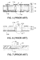
U.S. Pat. No. 7,033,862 B2, entitled “Method of Embedding Semiconductor Element in Carrier and Embedded Structure Thereof”, discloses a conventional method for embedding a semiconductor element in carrier including the following steps as follows. Firstly, a carrier 310 having a through hole 301 is provided, and an auxiliary material 311 is attached to a lower side of the carrier 310. A semiconductor element 312 is placed in the through hole 301 of the carrier 310. Then, a medium material 313 and a glue 314 are applied in order in the through hole 301 to firmly position the semiconductor element 312 in the hole 301 of the carrier 310 by the glue 314. Finally, the auxiliary material 311 and the medium material 313 are removed so as to form a structure with the semiconductor element 312 being embedded in the carrier 310, shown in FIG. 7, thereby eliminating the drawbacks encountered in packing the semiconductor element in the prior art. However, U.S. Pat. No. 7,033,862 B2 fails to disclose that the electrode 315 of the semiconductor element 312 (i.e. embedded component) is electrically connected to a circuit layer of a circuit board.
Accordingly, there exists a need for a method for manufacturing a circuit board having an embedded component therein, the method being capable of solving the above-mentioned problems.
SUMMARY OF THE INVENTION
It is an object of the present invention to provide a method for manufacturing a circuit board, the method decreasing the thickness of the electrode of the embedded component by a thickness decreasing process, whereby a patterned circuit layer can be electrically connected to the electrode certainly.
It is a further object of the present invention to provide a method for manufacturing a circuit board comprising the following steps of: providing a core layer, wherein the core layer includes a first dielectric layer, and first and second metallic layers, the first dielectric layer has upper and lower surfaces, and the first and second metallic layers are located on the upper and lower surfaces of the first dielectric layer respectively; forming a first through hole in the core layer; disposing the core layer on a supporting plate, and disposing an embedded component in the first through hole, wherein the second metallic layer contacts the supporting plate, and the embedded component has at least one electrode contacting the supporting plate; mounting the embedded component in the first through hole by an encapsulating process; removing the supporting plate; removing the first and second metallic layers and decreasing the thickness of the electrode of the embedded component by a thickness decreasing process; forming third and fourth metallic layers on the upper and lower surfaces of the first dielectric layer respectively, wherein the fourth metallic layer is electrically connected to the electrode of the embedded component; and patterning the third and fourth metallic layers so as to respectively form first and second patterned circuit layers.
According to the method of the present invention for manufacturing a circuit board, the electrode of he embedded component is located on the surface of the embedded component (the surface does not face the first dielectric layer). It is not necessary that the embedded component is electrically connected to the first surface circuit or the second surface circuit by a convention conductive via, whereby wiring areas on the first patterned circuit layer and the second patterned circuit layer can be increased, and further wiring densities on the first patterned circuit layer and the second patterned circuit layer can be increased. Furthermore, it is not necessary that the embedded component is electrically connected to the surface circuit by the convention conductive via, whereby the thickness of the whole circuit board cannot be increased. Thus, the circuit board can meet the requirements of light, thin, short and small product.
In addition, the method of the present invention for manufacturing a circuit board having an embedded component therein can decrease the thickness of the electrode of the embedded component by a thickness decreasing process, whereby the contacting surface of the electrode can be certainly exposed from the adhesive, i.e. residues of the adhesive on the contacting surface of the electrode can be certainly cleaned. Thus, the fourth metallic layer can be electrically connected to the electrode of the embedded component certainly, i.e. the second patterned circuit layer can be electrically connected to the contacting surface of the electrode of the embedded component certainly.
The foregoing, as well as additional objects, features and advantages of the invention will be more apparent from the following detailed description, which proceeds with reference to the accompanying drawings.
BRIEF DESCRIPTION OF THE DRAWINGS
FIGS. 1 to 5 are cross-sectional views showing a method for manufacturing a circuit board having an embedded component therein in the prior art.
FIG. 6 is a cross-sectional view showing another method for manufacturing a circuit board having an embedded component therein in the prior art.
FIG. 7 is a cross-sectional view showing a method for embedding a semiconductor element in carrier in the prior art.
FIG. 8 is a flow diagram showing a method for manufacturing a circuit board having an embedded component therein according to a first embodiment of the present invention.
FIGS. 9 to 18 are cross-sectional views showing a method for manufacturing a circuit board having an embedded component therein according to the first embodiment of the present invention.
FIG. 19 is a flow diagram showing a method for manufacturing a circuit board having an embedded component therein according to a second embodiment of the present invention.
FIGS. 20 to 26 are cross-sectional views showing a method for manufacturing a circuit board having an embedded component therein according to the second embodiment of the present invention.
DETAILED DESCRIPTION OF THE PREFERRED EMBODIMENT
Referring to FIG. 8, it depicts a method for manufacturing a circuit board having an embedded component therein according to a first embodiment of the present invention. Referring to FIG. 9, in the step 402 a core layer 510 is provided, wherein the core layer 510 includes a first dielectric layer 512, and first and second metallic layers 514, 516. The first dielectric layer 512 has an upper surface 512 a and a lower surface 512 b, the first and second metallic layers 514, 516 are located on the upper surface 512 a and the lower surface 512 b of the first dielectric layer 512 respectively. In this embodiment, the first and second metallic layers 514, 516 are made of copper (Cu) and have a thickness being equal to or less than 3 micrometer (μm).
Referring to FIG. 10, in the step 404 a first through hole 511 is formed in the core layer 510. For example, the first through hole 511 can be formed in the core layer 510 by mechanic drilling process or laser drilling process. In this embodiment, at least one second through hole 513 can be simultaneously formed in the core layer 510.
Referring to FIG. 11, in the step 406 the core layer 510 is disposed on a supporting plate 520, and an embedded component 530 is disposed in the first through hole 511. The second metallic layer 516 contacts the supporting plate 520. The embedded component 530 can be an active component or a passive component. The embedded component 530 has a surface 532 and at least one electrode 534, wherein the electrode 534 is located on the surface 532 and contacts the supporting plate 520. The surface 532 does not face the first dielectric layer 512, i.e. the surface 532 faces the supporting plate 520. In this embodiment, the supporting plate 520 can be made of glass or polyethylene terephthalate (PET). In the step 408 the embedded component 530 is mounted in the first through hole 511 by an encapsulating process. In this encapsulating process, an adhesive 522 is filled in the gap between the embedded component 530 and the first through hole 511.
Referring to FIG. 12, in the step 410 the supporting plate 520 is removed. Referring to FIG. 13, in the step 412 the first and second metallic layers 514, 516 are removed (i.e. the thickness of the core layer 510 is decreased), and the thickness of the electrode 534 of the embedded component 530 is decreased by a thickness decreasing process, wherein the thickness difference of the decreased electrode 534 is equal to the thickness of the second metallic layer 516 of the core layer 510. For example, the thickness decreasing process can be a grinding process or a flash etching process for removing the first and second metallic layers 514, 516 and decreasing the thickness of the electrode 534 of the embedded component 530. In this embodiment, if the original thickness of the electrode 534 is more than 10 micrometer (μm) and the thickness difference of the decreased electrode 534 is 3 micrometer by a grinding device 540 (i.e. the thickness of the second metallic layers 516 is equal to 3 micrometer), the thickness of the decreased electrode 534 is still more than 7 micrometer, whereby the contacting surface 536 of the electrode 534 can be certainly exposed from the adhesive 522, i.e. residues of the adhesive 522 on the contacting surface 536 of the electrode 534 can be certainly cleaned.
Referring to FIG. 14, in the step 414 third and fourth metallic layers 542, 544 are formed on the upper and lower surfaces 215 a, 512 b of the first dielectric layer 512 respectively, wherein the fourth metallic layer 542 is electrically connected to the electrode 534 of the embedded component 530. The contacting surface 536 of the electrode 534 is exposed from the adhesive 522 certainly, and thus the fourth metallic layer 542 is electrically connected to the contacting surface 536 of the electrode 534 certainly. In this embodiment, a first conductive via 546 can be simultaneously formed from the second through hole 513. The third and fourth metallic layers 542, 544 can be made of copper (Cu).
Referring to FIG. 15, in the step 416 the third and fourth metallic layers 542, 544 are patterned so as to respectively form first and second patterned circuit layers 542′, 544′. For example, the third and fourth metallic layers 542, 544 are patterned to the first and second patterned circuit layers 542′, 544′ by photolithography and etching processes.
Referring to FIG. 16, in the step 418 first and second stacking layers 550, 560 are disposed on the first and second patterned circuit layers 542′, 544′ respectively, wherein the first stacking layer 550 includes a fifth metallic layer 552 and a second dielectric layer 554, the second stacking layer 560 includes a sixth metallic layer 562 and a third dielectric layer 564, and the second and third dielectric layers 554, 564 face the first and second patterned circuit layers 542′, 544′ respectively.
Referring to FIG. 17, in the step 420 the first stacking layer 550, the core layer 510 and the second stacking layer 560 are laminated. In the step 422 second and third conductive vias 556, 566 are formed in the first stacking layer 550 and the second stacking layer 560 respectively. In the step 424 the fifth metallic layer 552 and sixth metallic layer 562 are patterned so as to respectively form a first surface circuit 552′ and a second surface circuit 562′. Also, the first surface circuit 552′ and the second surface circuit 562′ are electrically connected to each other by the first, second and third conductive vias 546, 556, 566.
Referring to FIG. 18, in the step 426 a first solder mask 572 and a second solder mask 574 are formed on the second dielectric layer 554 and the third dielectric layer 564 respectively, wherein the first solder mask 572 exposes at least one part of the first surface circuit 552′, and the second solder mask 574 exposes at least one part of the second surface circuit 562′.
In the step 428 a first anti-oxidative layer 576 is formed on the exposed part of the first surface circuit 552′, and a second anti-oxidative layer 578 is formed on the exposed part of the second surface circuit 562′. The first and second anti-oxidative layers 576, 578 can be nickel (Ni) and gold (Au) layers, which are formed on the exposed parts of the first surface circuit 552′ and the second surface circuit 562′ respectively by electroplating processes.
According to the method of the present invention for manufacturing a circuit board having an embedded component therein, the electrode of he embedded component is located on the surface of the embedded component (the surface does not face the first dielectric layer). It is not necessary that the embedded component is electrically connected to the first surface circuit or the second surface circuit by a convention conductive via, whereby wiring areas on the first patterned circuit layer and the second patterned circuit layer can be increased, and further wiring densities on the first patterned circuit layer and the second patterned circuit layer can be increased. Furthermore, it is not necessary that the embedded component is electrically connected to the surface circuit by the convention conductive via, whereby the thickness of the whole circuit board cannot be increased. Thus, the circuit board can meet the requirements of light, thin, short and small product.
In addition, the method of the present invention for manufacturing a circuit board having an embedded component therein can decrease the thickness of the electrode of the embedded component by a thickness decreasing process, whereby the contacting surface of the electrode can be certainly exposed from the adhesive, i.e. residues of the adhesive on the contacting surface of the electrode can be certainly cleaned. Thus, the fourth metallic layer can be electrically connected to the electrode of the embedded component certainly, i.e. the second patterned circuit layer can be electrically connected to the contacting surface of the electrode of the embedded component certainly.
Referring to FIG. 19, it depicts a method for manufacturing a circuit board having an embedded component therein according to a second embodiment of the present invention. Referring to FIG. 20, in the step 602 a core layer 710 is provided, wherein the core layer 710 includes first, second and third dielectric layers 712, 754, 764, first and second patterned circuit layers 742′, 744′, and at least one first conductive via 746. The first dielectric layer 712 has an upper surface 712 a and a lower surface 712 b, and the first and second patterned circuit layers 742′, 744′ are located on the upper surface 712 a and the lower surface 712 b of the first dielectric layer 712 respectively. The second dielectric layer 754 is disposed on the upper surface 712 a of the first dielectric layer 712, and covers the first patterned circuit layer 742′. The third dielectric layer 764 is disposed on the lower surface 712 b of the first dielectric layer 712, and covers the second patterned circuit layer 744′. The first conductive via 746 is adapted to electrically connect the first patterned circuit layer 742′ to the second patterned circuit layer 744′.
Referring to FIG. 21, in the step 604 a through hole 711 is formed in the core layer 710. For example, the through hole 711 can be formed in the core layer 710 by mechanic drilling process or laser drilling process.
Referring to FIG. 22, in the step 606 the core layer 710 is disposed on a supporting plate 720, and an embedded component 730 is disposed in the through hole 711. The third dielectric layer 764 contacts the supporting plate 720. The embedded component 730 can be an active component or a passive component. The embedded component 730 has a surface 732 and at least one electrode 734, wherein the electrode 734 is located on the surface 732 and contacts the supporting plate 720. The surface 732 does not face the first dielectric layer 712, i.e. the surface 732 faces the supporting plate 720. In this embodiment, the supporting plate 720 can be made of glass or polyethylene terephthalate (PET). In the step 608 the embedded component 730 is mounted in the through hole 711 by an encapsulating process. In this encapsulating process, an adhesive 722 is filled in the gap between the embedded component 730 and the through hole 711.
Referring to FIG. 23, in the step 610 the supporting plate 720 is removed. Referring to FIG. 24, in the step 612 the thickness of the third dielectric layer 764 of the core layer 710 is decreased (i.e. the thickness of the core layer 710 is decreased), and the thickness of the electrode 734 of the embedded component 730 is decreased by a thickness decreasing process, wherein the thickness difference of the decreased electrode 734 is equal to the thickness difference of the decreased third dielectric layer 764 of the core layer 710. For example, the thickness decreasing process can be a grinding process or a flash etching process for decreasing the thickness of the third dielectric layer 764 of the core layer 710 and decreasing the thickness of the electrode 734 of the embedded component 730. In this embodiment, the thickness difference of the decreased electrode 734 is equal to the thickness difference of the decreased third dielectric layer 764 of the core layer 710 by a grinding device 740, whereby the contacting surface 736 of the electrode 734 can be certainly exposed from the adhesive 722, i.e. residues of the adhesive 722 on the contacting surface 736 of the electrode 734 can be certainly cleaned.
Referring to FIG. 24, in the step 614 first and second metallic layers 752, 762 are formed on the second and third dielectric layer 754, 764 respectively, wherein the second metallic layer 762 is electrically connected to the electrode 734 of the embedded component 730. The contacting surface 736 of the electrode 734 is exposed from the adhesive 722 certainly, and thus the second metallic layer 762 is electrically connected to the contacting surface 736 of the electrode 734 certainly. In this embodiment, second and third conductive vias 756, 766 can be simultaneously formed in the second and third dielectric layer 754, 764 respectively. The first and second metallic layers 752, 762 can be made of copper (Cu). Referring to FIG. 25, in the step 616 the first and second metallic layers 752, 762 are patterned so as to respectively form first and second surface circuits 752′, 762′, wherein the first and second surface circuits 752′, 762′ are electrically connected to each other by the first, second and third conductive vias 746, 756, 766.
Referring to FIG. 26, in the step 618 a first solder mask 772 and a second solder mask 774 are respectively formed on the second dielectric layer 754 and the third dielectric layer 764, wherein the first solder mask 772 exposes at least one part of the first surface circuit 752′, and the second solder mask 774 exposes at least one part of the second surface circuit 762′. In the step 620 a first anti-oxidative layer 776 is formed on the exposed part of the first surface circuit 752′, and a second anti-oxidative layer 778 is formed on the exposed part of the second surface circuit 762′.
According to the method of the present invention for manufacturing a board having an embedded component therein, the electrode of he embedded component is located on the surface of the embedded component (the surface does not face the first dielectric layer). It is not necessary that the embedded component is electrically connected to the first surface circuit or the second surface circuit by a convention conductive via, whereby wiring areas on the first patterned circuit layer and the second patterned circuit layer can be increased, and further wiring densities on the first patterned circuit layer and the second patterned circuit layer can be increased. Furthermore, it is not necessary that the embedded component is electrically connected to the surface circuit by the convention conductive via, whereby the thickness of the whole circuit board cannot be increased. Thus, the circuit board can meet the requirements of light, thin, short and small product.
In addition, the method of the present invention for manufacturing a board having an embedded component therein can decrease the thickness of the electrode of the embedded component by a thickness decreasing process, whereby the contacting surface of the electrode can be certainly exposed from the adhesive, i.e. residues of the adhesive on the contacting surface of the electrode can be certainly cleaned. Thus, the second metallic layer can be electrically connected to the electrode of the embedded component certainly, i.e. the second surface circuit can be electrically connected to the contacting surface of the electrode of the embedded component certainly.
Although the invention has been explained in relation to its preferred embodiment, it is not used to limit the invention. It is to be understood that many other possible modifications and variations can be made by those skilled in the art without departing from the spirit and scope of the invention as hereinafter claimed.

Claims (18)

1. A method for manufacturing a circuit board comprising the following steps of:
providing a core layer, wherein the core layer includes a first dielectric layer, and first and second metallic layers, the first dielectric layer has upper and lower surfaces, and the first and second metallic layers are located on the upper and lower surfaces of the first dielectric layer respectively;
forming a first through hole in the core layer;
disposing the core layer on a supporting plate, and disposing an embedded component in the first through hole, wherein the second metallic layer contacts the supporting plate, and the embedded component has at least one electrode contacting the supporting plate;
mounting the embedded component in the first through hole by an encapsulating process;
removing the supporting plate;
removing the first and second metallic layers and decreasing the thickness of the electrode of the embedded component by a thickness decreasing process;
forming third and fourth metallic layers on the upper and lower surfaces of the first dielectric layer respectively, wherein the fourth metallic layer is electrically connected to the electrode of the embedded component; and
patterning the third and fourth metallic layers so as to respectively form first and second patterned circuit layers.
2. The method as claimed in claim 1, wherein during the step of decreasing the thickness of the electrode, the thickness difference of the decreased electrode is equal to the thickness of the second metallic layer.
3. The method as claimed in claim 1, wherein the thickness decreasing process is one of a grinding process and a flash etching process.
4. The method as claimed in claim 1, wherein the encapsulating process comprises the step of filling an adhesive in the gap between the embedded component and the first through hole.
5. The method as claimed in claim 1, wherein the embedded component has a surface facing the supporting plate, and the electrode is located on the surface of the embedded component.
6. The method as claimed in claim 1, wherein during the step of forming the first through hole in the core layer, and the method further comprising the step of:
simultaneously forming at least one second through hole in the core layer.
7. The method as claimed in claim 6, wherein during the step of respectively forming third and fourth metallic layers on the upper and lower surfaces of the first dielectric layer, and the method further comprising the step of:
simultaneously forming a first conductive via from the second through hole.
8. The method as claimed in claim 1, wherein after the step of forming first and second patterned circuit layers, and the method further comprising the steps of:
desposing first and second stacking layers on the first and second patterned circuit layers respectively, wherein the first stacking layer includes a fifth metallic layer and a second dielectric layer, the second stacking layer includes a sixth metallic layer and a third dielectric layer, and the second and third dielectric layers face the first and second patterned circuit layers respectively;
laminating the first stacking layer, the core layer and the second stacking layer;
forming second and third conductive vias in the first stacking layer and the second stacking layer respectively; and
patterning the fifth metallic layer and sixth metallic layer so as to respectively form a first surface circuit and a second surface circuit, wherein the first surface circuit and the second surface circuit are electrically connected to each other by the first, second and third conductive vias.
9. A method for manufacturing a circuit board comprising the following steps of:
providing a core layer, wherein the core layer includes first, second and third dielectric layers, first and second patterned circuit layers and at least one first conductive via, the first dielectric layer has upper and lower surfaces, the first and second patterned circuit layers are located on the upper and lower surfaces of the first dielectric layer respectively, the second dielectric layer is disposed on the upper surface of the first dielectric layer and covers the first patterned circuit layer, the third dielectric layer is disposed on the lower surface of the first dielectric layer and covers the second patterned circuit layer, and the first conductive via is adapted to electrically connect the first patterned circuit layer to the second patterned circuit layer;
forming a first through hole in the core layer;
disposing the core layer on a supporting plate, and disposing an embedded component in the through hole, wherein the third dielectric layer contacts the supporting plate, and the embedded component has at least one electrode contacting the supporting plate;
mounting the embedded component in the through hole by an encapsulating process;
removing the supporting plate;
decreasing the thickness of the third dielectric layer of the core layer and the thickness of the electrode of the embedded component by a thickness decreasing process;
forming first and second metallic layers on the second and third dielectric layers respectively, wherein the second metallic layer is electrically connected to the electrode of the embedded component; and
patterning the first and second metallic layers so as to respectively form first and second surface circuits.
10. The method as claimed in claim 9, wherein during the step of decreasing the thickness of the third dielectric layer of the core layer and the thickness of the electrode of the embedded component, the thickness difference of the decreased electrode is equal to the thickness difference of the decreased third dielectric layer.
11. The method as claimed in claim 9, wherein the thickness decreasing process is one of a grinding process and a flash etching process.
12. The method as claimed in claim 9, wherein the encapsulating process comprises the step of filling an adhesive in the gap between the embedded component and the through hole.
13. The method as claimed in claim 9, wherein the embedded component has a surface facing the supporting plate, and the electrode is located on the surface of the embedded component.
14. The method as claimed in claim 9, wherein during the step of forming first and second metallic layers on the second and third dielectric layer respectively, and the method further comprising the step of:
simultaneously forming second and third conductive vias in the second and third dielectric layer respectively, wherein the first surface circuit and the second surface circuit are electrically connected to each other by the first, second and third conductive vias.
15. A method for decreasing a thickness of an electrode of an embedded component of a circuit board comprising the following steps of:
providing a core layer;
forming a through hole in the core layer;
disposing the core layer on a supporting plate, and disposing an embedded component in the through hole, wherein the embedded component has at least one electrode contacting the supporting plate;
mounting the embedded component in the through hole by an encapsulating process;
removing the supporting plate; and
decreasing a thickness of the core layer and the thickness of the electrode of the embedded component by a thickness decreasing process;
wherein a thickness difference of the decreased electrode is equal to a thickness difference of the decreased core layer.
16. The method as claimed in claim 15, wherein the thickness decreasing process is one of a grinding process and a flash etching process.
17. The method as claimed in claim 15, wherein the encapsulating process comprises the step of filling an adhesive in the gap between the embedded component and the through hole.
18. The method as claimed in claim 15, wherein the embedded component has a surface facing the supporting plate, and the electrode is located on the surface of the embedded component.
US12/142,853 2008-04-02 2008-06-20 Method for manufacturing a circuit board having an embedded component therein Active 2030-10-15 US8099865B2 (en)

Applications Claiming Priority (3)

Application Number Priority Date Filing Date Title
TW97111985A 2008-04-02
TW097111985A TWI363585B (en) 2008-04-02 2008-04-02 Method for manufacturing a substrate having embedded component therein
TW097111985 2008-04-02

Publications (2)

Publication Number Publication Date
US20090249618A1 US20090249618A1 (en) 2009-10-08
US8099865B2 true US8099865B2 (en) 2012-01-24

Family

ID=41131898

Family Applications (1)

Application Number Title Priority Date Filing Date
US12/142,853 Active 2030-10-15 US8099865B2 (en) 2008-04-02 2008-06-20 Method for manufacturing a circuit board having an embedded component therein

Country Status (2)

Country Link
US (1) US8099865B2 (en)
TW (1) TWI363585B (en)

Cited By (4)

* Cited by examiner, † Cited by third party
Publication number Priority date Publication date Assignee Title
US20130044448A1 (en) * 2011-08-18 2013-02-21 Biotronik Se & Co. Kg Method for Mounting a Component to an Electric Circuit Board, Electric Circuit Board and Electric Circuit Board Arrangement
US20150382478A1 (en) * 2013-02-12 2015-12-31 Meiko Electronics Co., Ltd. Device embedded substrate and manufacturing method of device embedded substrate
US20160007469A1 (en) * 2014-07-02 2016-01-07 Nan Ya Pcb Corporation Embedded component substrate and method for fabricating the same
US11044813B2 (en) * 2019-10-21 2021-06-22 Hongqisheng Precision Electronics (Qinhuangdao) Co., Ltd. All-directions embeded module, method for manufacturing the all-directions embeded module, and all-directions packaging structure

Families Citing this family (10)

* Cited by examiner, † Cited by third party
Publication number Priority date Publication date Assignee Title
KR101148601B1 (en) 2010-07-05 2012-05-25 삼성전기주식회사 IC Module and Method of Manufacturing the same, and Embedded Printed Circuit Board using IC Module and Method of Manufacturing the same
KR101326999B1 (en) 2012-03-07 2013-11-13 엘지이노텍 주식회사 The printed circuit board and the method for manufacturing the same
JP6133549B2 (en) * 2012-04-26 2017-05-24 新光電気工業株式会社 Wiring board and method of manufacturing wiring board
TWI473544B (en) * 2012-12-17 2015-02-11 Unimicron Technology Corp Embeded chip package structure
CN103904048B (en) * 2012-12-27 2017-03-01 欣兴电子股份有限公司 Embedded chips encapsulating structure
US9324664B2 (en) 2013-02-22 2016-04-26 Unimicron Technology Corp. Embedded chip package structure
CN104979325B (en) * 2014-04-04 2017-12-12 欣兴电子股份有限公司 It is embedded with encapsulating structure of passive type electronic component and preparation method thereof
CN107068634A (en) * 2017-01-23 2017-08-18 合肥雷诚微电子有限责任公司 A kind of multi-chip power amplifier architecture for minimizing high-cooling property and preparation method thereof
CN108962839B (en) * 2017-05-26 2021-02-19 欣兴电子股份有限公司 Packaging structure
TWI645519B (en) * 2017-06-02 2018-12-21 旭德科技股份有限公司 Component embedded package carrier and manufacturing method thereof

Citations (26)

* Cited by examiner, † Cited by third party
Publication number Priority date Publication date Assignee Title
US6194250B1 (en) * 1998-09-14 2001-02-27 Motorola, Inc. Low-profile microelectronic package
US6486537B1 (en) * 2001-03-19 2002-11-26 Amkor Technology, Inc. Semiconductor package with warpage resistant substrate
US20020185303A1 (en) * 2001-03-12 2002-12-12 Ngk Spark Plug Co., Ltd. Wiring circuit board and method for producing same
US6515356B1 (en) * 1999-05-07 2003-02-04 Amkor Technology, Inc. Semiconductor package and method for fabricating the same
US6586824B1 (en) * 2001-07-26 2003-07-01 Amkor Technology, Inc. Reduced thickness packaged electronic device
US20040020047A1 (en) * 2002-07-05 2004-02-05 Kazuhiro Nishikawa Multilayered circuit board forming method and multilayered circuit board
US20040045738A1 (en) * 2001-11-12 2004-03-11 Toshio Sugawa Audio coding and decoding
US6746894B2 (en) * 2001-03-30 2004-06-08 Micron Technology, Inc. Ball grid array interposer, packages and methods
US6790712B2 (en) * 2001-03-21 2004-09-14 United Test Center, Inc. Semiconductor device and method for fabricating the same
US6841423B2 (en) * 2000-06-28 2005-01-11 Micron Technology, Inc. Methods for formation of recessed encapsulated microelectronic devices
US7033862B2 (en) * 2004-06-29 2006-04-25 Phoenix Precision Technology Corporation Method of embedding semiconductor element in carrier and embedded structure thereof
US20060191711A1 (en) * 2005-02-28 2006-08-31 Samsung Electro-Mechanics Co., Ltd. Embedded chip printed circuit board and method of manufacturing the same
US20060248717A1 (en) * 2004-07-02 2006-11-09 Endicott Interconnect Technologies, Inc. Method of making circuitized substrate with filled isolation border
US20070143993A1 (en) * 2005-12-27 2007-06-28 Shih-Ping Hsu Substrate structure with capacitor component embedded therein and method for fabricating the same
US20080041619A1 (en) * 2006-08-17 2008-02-21 Samsung Electro-Mechanics Co., Ltd. Component-embedded multilayer printed wiring board and manufacturing method thereof
US7350296B2 (en) * 2004-09-15 2008-04-01 Samsung Electro-Mechanics Co., Ltd. Method of fabricating a printed circuit board including an embedded passive component
US20080220566A1 (en) * 2007-03-09 2008-09-11 Chueh-An Hsieh Substrate process for an embedded component
US7435910B2 (en) * 2000-02-25 2008-10-14 Ibiden Co., Ltd. Multilayer printed circuit board
TWI305479B (en) 2006-02-13 2009-01-11 Advanced Semiconductor Eng Method of fabricating substrate with embedded component therein
US7514770B2 (en) * 2005-10-18 2009-04-07 Phoenix Precision Technology Corporation Stack structure of carrier board embedded with semiconductor components and method for fabricating the same
US7525814B2 (en) * 2005-06-15 2009-04-28 Ngk Spark Plug Co., Ltd. Wiring board and method for manufacturing the same
US7594316B2 (en) * 2004-07-30 2009-09-29 Murata Manufacturing Co., Ltd. Method of manufacturing composite electronic component
US7649361B2 (en) * 2006-12-18 2010-01-19 E.I. Du Pont De Nemours And Company Methods for forming process test capacitors for testing embedded passives during embedment into a printed wiring board
US7653991B2 (en) * 2007-04-30 2010-02-02 Samsung Electro-Mechanics Co., Ltd. Method for manufacturing printed circuit board having embedded component
US7791174B2 (en) * 2008-03-07 2010-09-07 Advanced Inquiry Systems, Inc. Wafer translator having a silicon core isolated from signal paths by a ground plane
US20110061232A1 (en) * 2005-06-30 2011-03-17 Ibiden Co., Ltd. Printed wiring board

Patent Citations (27)

* Cited by examiner, † Cited by third party
Publication number Priority date Publication date Assignee Title
US6194250B1 (en) * 1998-09-14 2001-02-27 Motorola, Inc. Low-profile microelectronic package
US6515356B1 (en) * 1999-05-07 2003-02-04 Amkor Technology, Inc. Semiconductor package and method for fabricating the same
US7435910B2 (en) * 2000-02-25 2008-10-14 Ibiden Co., Ltd. Multilayer printed circuit board
US6841423B2 (en) * 2000-06-28 2005-01-11 Micron Technology, Inc. Methods for formation of recessed encapsulated microelectronic devices
US20020185303A1 (en) * 2001-03-12 2002-12-12 Ngk Spark Plug Co., Ltd. Wiring circuit board and method for producing same
US6512182B2 (en) * 2001-03-12 2003-01-28 Ngk Spark Plug Co., Ltd. Wiring circuit board and method for producing same
US6486537B1 (en) * 2001-03-19 2002-11-26 Amkor Technology, Inc. Semiconductor package with warpage resistant substrate
US6790712B2 (en) * 2001-03-21 2004-09-14 United Test Center, Inc. Semiconductor device and method for fabricating the same
US6746894B2 (en) * 2001-03-30 2004-06-08 Micron Technology, Inc. Ball grid array interposer, packages and methods
US6586824B1 (en) * 2001-07-26 2003-07-01 Amkor Technology, Inc. Reduced thickness packaged electronic device
US20040045738A1 (en) * 2001-11-12 2004-03-11 Toshio Sugawa Audio coding and decoding
US20040020047A1 (en) * 2002-07-05 2004-02-05 Kazuhiro Nishikawa Multilayered circuit board forming method and multilayered circuit board
US7033862B2 (en) * 2004-06-29 2006-04-25 Phoenix Precision Technology Corporation Method of embedding semiconductor element in carrier and embedded structure thereof
US20060248717A1 (en) * 2004-07-02 2006-11-09 Endicott Interconnect Technologies, Inc. Method of making circuitized substrate with filled isolation border
US7594316B2 (en) * 2004-07-30 2009-09-29 Murata Manufacturing Co., Ltd. Method of manufacturing composite electronic component
US7350296B2 (en) * 2004-09-15 2008-04-01 Samsung Electro-Mechanics Co., Ltd. Method of fabricating a printed circuit board including an embedded passive component
US20060191711A1 (en) * 2005-02-28 2006-08-31 Samsung Electro-Mechanics Co., Ltd. Embedded chip printed circuit board and method of manufacturing the same
US7525814B2 (en) * 2005-06-15 2009-04-28 Ngk Spark Plug Co., Ltd. Wiring board and method for manufacturing the same
US20110061232A1 (en) * 2005-06-30 2011-03-17 Ibiden Co., Ltd. Printed wiring board
US7514770B2 (en) * 2005-10-18 2009-04-07 Phoenix Precision Technology Corporation Stack structure of carrier board embedded with semiconductor components and method for fabricating the same
US20070143993A1 (en) * 2005-12-27 2007-06-28 Shih-Ping Hsu Substrate structure with capacitor component embedded therein and method for fabricating the same
TWI305479B (en) 2006-02-13 2009-01-11 Advanced Semiconductor Eng Method of fabricating substrate with embedded component therein
US20080041619A1 (en) * 2006-08-17 2008-02-21 Samsung Electro-Mechanics Co., Ltd. Component-embedded multilayer printed wiring board and manufacturing method thereof
US7649361B2 (en) * 2006-12-18 2010-01-19 E.I. Du Pont De Nemours And Company Methods for forming process test capacitors for testing embedded passives during embedment into a printed wiring board
US20080220566A1 (en) * 2007-03-09 2008-09-11 Chueh-An Hsieh Substrate process for an embedded component
US7653991B2 (en) * 2007-04-30 2010-02-02 Samsung Electro-Mechanics Co., Ltd. Method for manufacturing printed circuit board having embedded component
US7791174B2 (en) * 2008-03-07 2010-09-07 Advanced Inquiry Systems, Inc. Wafer translator having a silicon core isolated from signal paths by a ground plane

Cited By (5)

* Cited by examiner, † Cited by third party
Publication number Priority date Publication date Assignee Title
US20130044448A1 (en) * 2011-08-18 2013-02-21 Biotronik Se & Co. Kg Method for Mounting a Component to an Electric Circuit Board, Electric Circuit Board and Electric Circuit Board Arrangement
US20150382478A1 (en) * 2013-02-12 2015-12-31 Meiko Electronics Co., Ltd. Device embedded substrate and manufacturing method of device embedded substrate
US20160007469A1 (en) * 2014-07-02 2016-01-07 Nan Ya Pcb Corporation Embedded component substrate and method for fabricating the same
US9894779B2 (en) * 2014-07-02 2018-02-13 Nan Ya Pcb Corp. Embedded component substrate and method for fabricating the same
US11044813B2 (en) * 2019-10-21 2021-06-22 Hongqisheng Precision Electronics (Qinhuangdao) Co., Ltd. All-directions embeded module, method for manufacturing the all-directions embeded module, and all-directions packaging structure

Also Published As

Publication number Publication date
TW200944072A (en) 2009-10-16
US20090249618A1 (en) 2009-10-08
TWI363585B (en) 2012-05-01

Similar Documents

Publication Publication Date Title
US8099865B2 (en) Method for manufacturing a circuit board having an embedded component therein
US7550320B2 (en) Method of fabricating substrate with embedded component therein
US8177577B2 (en) Printed wiring board having a substrate with higher conductor density inserted into a recess of another substrate with lower conductor density
US7338892B2 (en) Circuit carrier and manufacturing process thereof
US7377030B2 (en) Wiring board manufacturing method
US20100142170A1 (en) Chip embedded printed circuit board and manufacturing method thereof
JP2006108211A (en) Wiring board, multilayered wiring circuit board using the board, and method of manufacturing the multilayered wiring circuit board
US10249503B2 (en) Printed circuit board, semiconductor package and method of manufacturing the same
CN102771200A (en) Multilayer printed circuit board and manufacturing method therefor
US9899235B2 (en) Fabrication method of packaging substrate
JP2003264253A (en) Semiconductor device and method of manufacturing the same
JP2008112996A (en) Method of manufacturing printed-circuit substrate
US20090025210A1 (en) Circuit board structure with concave conductive cylinders and method for fabricating the same
US9839132B2 (en) Component-embedded substrate
US9578749B2 (en) Element embedded printed circuit board and method of manufacturing the same
KR101164957B1 (en) PCB within cavity and Fabricaring method of the same
KR20150102504A (en) Embedded board and method of manufacturing the same
KR101669534B1 (en) Circuit board with bumps and method of manufacturing the same
US20120266463A1 (en) Method for manufacturing printed circuit board
JP2007053146A (en) Sealed printed board and its manufacturing method
KR102052761B1 (en) Chip Embedded Board And Method Of Manufacturing The Same
JP2013115110A (en) Printed wiring board of step structure
JP4806926B2 (en) Manufacturing method of electronic component mounting apparatus
JP2623980B2 (en) Manufacturing method of substrate with lead for semiconductor mounting
KR101969643B1 (en) Rigid flexible circuit board manufacturing method

Legal Events

Date Code Title Description
AS Assignment

Owner name: ADVANCED SEMICONDUCTOR ENGINEERING, INC., TAIWAN

Free format text: ASSIGNMENT OF ASSIGNORS INTEREST;ASSIGNORS:WANG, YUNG HUI;OU, YING TE;REEL/FRAME:021124/0472

Effective date: 20080507

STCF Information on status: patent grant

Free format text: PATENTED CASE

FPAY Fee payment

Year of fee payment: 4

MAFP Maintenance fee payment

Free format text: PAYMENT OF MAINTENANCE FEE, 8TH YEAR, LARGE ENTITY (ORIGINAL EVENT CODE: M1552); ENTITY STATUS OF PATENT OWNER: LARGE ENTITY

Year of fee payment: 8

MAFP Maintenance fee payment

Free format text: PAYMENT OF MAINTENANCE FEE, 12TH YEAR, LARGE ENTITY (ORIGINAL EVENT CODE: M1553); ENTITY STATUS OF PATENT OWNER: LARGE ENTITY

Year of fee payment: 12